Embed Size (px)
Citation preview
Title Power conversion with SiC devices at extremely high ambienttemperatures
Author(s) Funaki, T; Balda, JC; Junghans, J; Kashyap, AS; Mantooth,HA; Barlow, F; Kimoto, T; Hikihara, T
Citation IEEE TRANSACTIONS ON POWER ELECTRONICS(2007), 22(4): 1321-1329
Issue Date 2007-07
URL http://hdl.handle.net/2433/50531
Right
(c)2007 IEEE. Personal use of this material is permitted.However, permission to reprint/republish this material foradvertising or promotional purposes or for creating newcollective works for resale or redistribution to servers or lists,or to reuse any copyrighted component of this work in otherworks must be obtained from the IEEE.
Type Journal Article
Textversion publisher
Kyoto University
IEEE TRANSACTIONS ON POWER ELECTRONICS, VOL. 22, NO. 4, JULY 2007 1321
Power Conversion With SiC Devices at ExtremelyHigh Ambient Temperatures
Tsuyoshi Funaki, Member, IEEE, Juan Carlos Balda, Senior Member, IEEE, Jeremy Junghans, Member, IEEE,Avinash S. Kashyap, Student Member, IEEE, H. Alan Mantooth, Senior Member, IEEE, Fred Barlow, Member, IEEE,
Tsunenobu Kimoto, Member, IEEE, and Takashi Hikihara, Member, IEEE
Abstract—This paper evaluates the capability of SiC power semi-conductor devices, in particular JFET and Schottky barrier diodes(SBD) for application in high-temperature power electronics. SiCJFETs and SBDs were packaged in high temperature packages tomeasure the dc characteristics of these SiC devices at ambient tem-peratures ranging from 25 C (room temperature) up to 450 C.The results show that both devices can operate at 450 C, which isimpossible for conventional Si devices, at the expense of significantderating. The current capability of the SiC SBD does not changewith temperature, but as expected the JFET current decreases withrising temperatures. A 100V, 25W dc-dc converter is used as anexample of a high-temperature power-electronics circuit becauseof circuit simplicity. The converter is designed and built in accor-dance with the static characteristics of the SiC devices measuredunder extremely high ambient temperatures, and then tested up toan ambient temperature of 400 C. The conduction loss of the SiCJFET increases slightly with increasing temperatures, as predictedfrom its dc characteristics, but its switching characteristics hardlychange. Thus, SiC devices are well suited for operation in harshtemperature environments like aerospace and automotive applica-tions.
Index Terms—dc-dc converter circuit, device characterization,high temperature operation, packaging, silicon carbide (SiC) de-vice.
I. INTRODUCTION
SILICON CARBIDE (SiC) has several superior characteris-tics over silicon (Si) when used as a semiconductor material
[1]–[6]. In particular, SiC semiconductor devices are expected
Manuscript received February 10, 2006. The work of T. Funaki was supportedin part by the Ministry of Education, Culture, Sports, Sciences and Technologyin Japan, the Grant-in-Aid for Scientific Research 17686024 and in part by the21st Century COE Program 14213201, Japan. The work of J. C. Balda, J. Jung-hans, A. Kashyap, H. A. Mantooth, and F. Barlow was supported in part bythe Office of Naval Research under Award N00014-04-1-0603 and in part bythe National Science Foundation under Award ECS-0424411. Recommendedby Associate Editor Y. C. Liang. This paper was presented at the IEEE 36thAnnu. Power Electronics Specialists Conference (PESC), Recife, Brazil, June12–16, 2005, pp. 2030–2035.
T. Funaki and T. Hikihara are with Department of Electrical Engineering,Graduate School of Engineering, Kyoto University, Kyoto 615-8510, Japan(e-mail: [email protected]; [email protected]).
J. C. Balda, A. S. Kashyap, and H. A. Mantooth are with Department ofElectrical Engineering, University of Arkansas, Fayetteville, AR 72701 USA(e-mail: [email protected]; [email protected]; [email protected]).
J. Junghans is with RF Power Devices Group, Northrop Grumman ElectronicSystems, Baltimore, MD 21203 USA (e-mail: [email protected]).
F. Barlow is with the Electrical and Computer Engineering Department, Uni-versity of Idaho, Moscow, ID 83844 USA (e-mail: [email protected]).
T. Kimoto is with the Department of Electronic Science and Engineering,Graduate School of Engineering, Kyoto University, Kyoto 615-8510, Japan(e-mail: [email protected]).
Digital Object Identifier 10.1109/TPEL.2007.900561
TABLE ISIC DEVICE PARAMETERS
to have high temperature, high speed and high voltage operationcapabilities [7], which are attributed to the wide bandgap prop-erties of SiC. These advantages cannot all be obtained with con-ventional Si-based semiconductor devices. This paper focuseson the high temperature operation capability of SiC devices andtheir switching characteristics in a dc-dc buck converter. SiCJFETs and Schottky barrier diodes (SBD) are specifically ad-dressed in this work.
Several publications have indicated that SiC semiconductordevices are suitable for high temperature operation [8]–[13],[15], [16]. However, most publications cover the study of lowpower devices like op-amps [8], sensors [9], or integrated cir-cuits [10]. There are a few studies on power converters, but theyare limited to temperatures under 250 C [11]–[15]. Further-more, there has been no report on the operation of gate control-lable devices such as JFETs at extremely high ambient temper-atures. The two main reasons are that (a) the SiC JFET is stillunder development, and (b) the difficulty of packaging bare diefor high temperature operation. The latter requires not only thatthe SiC bare die be capable of operation at high temperatures,but also the package material (including the die attach and wirebonds) and the auxiliary circuit components (e.g., gate driver).Otherwise, the converter can only operate up to ambient tem-peratures no greater than 250 C.
SiC JFETs and SBDs were packaged in dedicated thermallystable packages. The dc characteristics of the SiC JFET andSBD under extremely high ambient temperature conditions upto 450 C were then evaluated using an automated experimentalsetup for high temperature measurements. The current ratingsof the dc-dc buck converter were determined from the exper-imental results since derating occurs in the SiC JFET with in-creasing temperatures. The converter inductor was designed andbuilt using a high-temperature toroidal magnetic core and high-temperature wires. Testing was done up to ambient temperaturesof 400 C using a resistive load in order to evaluate the switching
0885-8993/$25.00 © 2007 IEEE
1322 IEEE TRANSACTIONS ON POWER ELECTRONICS, VOL. 22, NO. 4, JULY 2007
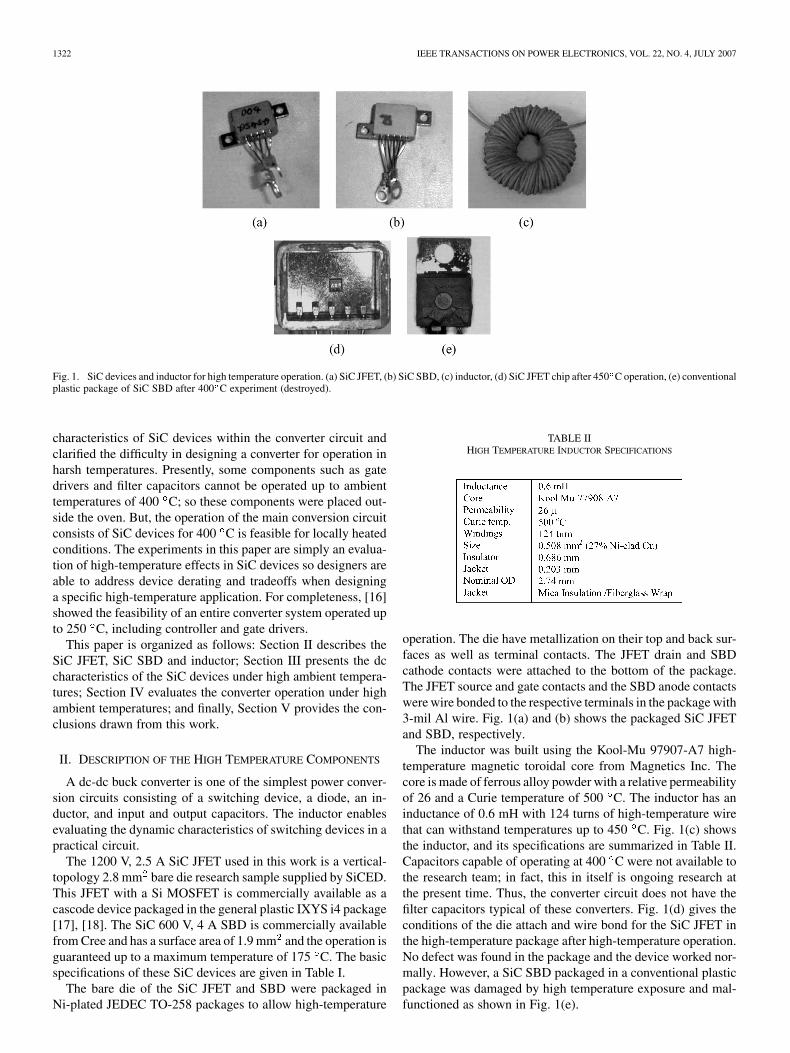
Fig. 1. SiC devices and inductor for high temperature operation. (a) SiC JFET, (b) SiC SBD, (c) inductor, (d) SiC JFET chip after 450 C operation, (e) conventionalplastic package of SiC SBD after 400 C experiment (destroyed).
characteristics of SiC devices within the converter circuit andclarified the difficulty in designing a converter for operation inharsh temperatures. Presently, some components such as gatedrivers and filter capacitors cannot be operated up to ambienttemperatures of 400 C; so these components were placed out-side the oven. But, the operation of the main conversion circuitconsists of SiC devices for 400 C is feasible for locally heatedconditions. The experiments in this paper are simply an evalua-tion of high-temperature effects in SiC devices so designers areable to address device derating and tradeoffs when designinga specific high-temperature application. For completeness, [16]showed the feasibility of an entire converter system operated upto 250 C, including controller and gate drivers.
This paper is organized as follows: Section II describes theSiC JFET, SiC SBD and inductor; Section III presents the dccharacteristics of the SiC devices under high ambient tempera-tures; Section IV evaluates the converter operation under highambient temperatures; and finally, Section V provides the con-clusions drawn from this work.
II. DESCRIPTION OF THE HIGH TEMPERATURE COMPONENTS
A dc-dc buck converter is one of the simplest power conver-sion circuits consisting of a switching device, a diode, an in-ductor, and input and output capacitors. The inductor enablesevaluating the dynamic characteristics of switching devices in apractical circuit.
The 1200 V, 2.5 A SiC JFET used in this work is a vertical-topology 2.8 mm bare die research sample supplied by SiCED.This JFET with a Si MOSFET is commercially available as acascode device packaged in the general plastic IXYS i4 package[17], [18]. The SiC 600 V, 4 A SBD is commercially availablefrom Cree and has a surface area of 1.9 mm and the operation isguaranteed up to a maximum temperature of 175 C. The basicspecifications of these SiC devices are given in Table I.
The bare die of the SiC JFET and SBD were packaged inNi-plated JEDEC TO-258 packages to allow high-temperature
TABLE IIHIGH TEMPERATURE INDUCTOR SPECIFICATIONS
operation. The die have metallization on their top and back sur-faces as well as terminal contacts. The JFET drain and SBDcathode contacts were attached to the bottom of the package.The JFET source and gate contacts and the SBD anode contactswere wire bonded to the respective terminals in the package with3-mil Al wire. Fig. 1(a) and (b) shows the packaged SiC JFETand SBD, respectively.
The inductor was built using the Kool-Mu 97907-A7 high-temperature magnetic toroidal core from Magnetics Inc. Thecore is made of ferrous alloy powder with a relative permeabilityof 26 and a Curie temperature of 500 C. The inductor has aninductance of 0.6 mH with 124 turns of high-temperature wirethat can withstand temperatures up to 450 C. Fig. 1(c) showsthe inductor, and its specifications are summarized in Table II.Capacitors capable of operating at 400 C were not available tothe research team; in fact, this in itself is ongoing research atthe present time. Thus, the converter circuit does not have thefilter capacitors typical of these converters. Fig. 1(d) gives theconditions of the die attach and wire bond for the SiC JFET inthe high-temperature package after high-temperature operation.No defect was found in the package and the device worked nor-mally. However, a SiC SBD packaged in a conventional plasticpackage was damaged by high temperature exposure and mal-functioned as shown in Fig. 1(e).
FUNAKI et al.: POWER CONVERSION WITH SIC DEVICES AT EXTREMELY HIGH AMBIENT TEMPERATURES 1323
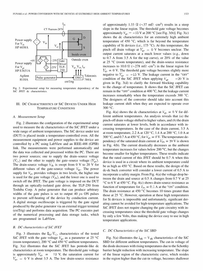
Fig. 2. Experimental setup for measuring temperature dependency of theSiC JFET dc characteristics.
III. DC CHARACTERISTICS OF SIC DEVICES UNDER HIGH
TEMPERATURE CONDITIONS
A. Measurement Setup
Fig. 2 illustrates the configuration of the experimental setupused to measure the dc characteristics of the SiC JFET under awide range of ambient temperatures. The SiC device under test(DUT) is placed inside a temperature-controlled oven. All themeasurement equipment and power supplies to the device arecontrolled by a PC using LabView and an IEEE-488 (GPIB)link. The measurements were performed automatically andthe data was collected and processed within the PC. There aretwo power sources; one to supply the drain–source voltage
and the other to supply the gate–source voltage .The drain-source voltage is swept from 0 V to 20 V fordifferent values of the gate-source voltage . The powersupply for provides voltages in two levels, the higher oneis used for the gate voltage , and the lower one is used toswitch off the JFET. The gate voltage is imposed on the DUTthrough an optically-isolated gate driver, the TLP-250 fromToshiba Corp. A pulse generator that can produce arbitrarywidths of the gate pulses is set to output 40 s ON pulsesto prevent self-heating of the device by conduction current.A digital storage oscilloscope is triggered by the gate signalproduced by the pulse generator via an external trigger terminal(extTrig) and performs data acquisition. The PC executes partof the numerical processing and data storage tasks, whichare programmed in LabView.
B. DC characteristics of SiC JFET
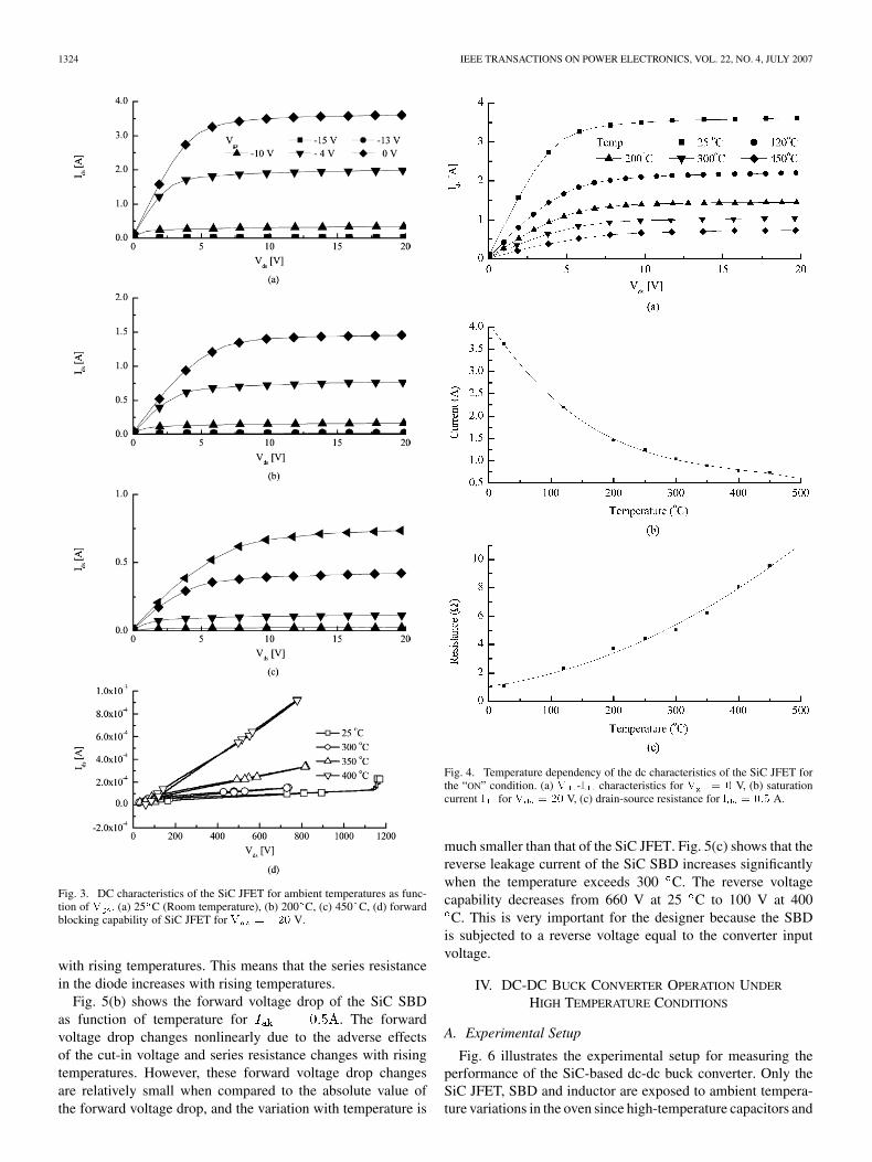
Fig. 3 illustrates the - characteristics of the testedSiC JFET with the gate voltage as a parameter at 25 C(room temperature), 200 C and 450 C ambient temperatures.Fig. 3(a) illustrates that the SiC JFET has pentode-like dccharacteristics at room temperature. The threshold gate voltageis approximately V, the saturation current for
V is about 3.5 A. The low drain-source resistance
of approximately 1.33 ( 37 m -cm ) results in a steepslope in the linear region. The threshold gate voltage becomesapproximately V at 200 C [see Fig. 3(b)]. Fig. 3(c)shows the dc characteristics for an extremely high ambienttemperature of 450 C, which is far beyond the temperaturecapability of Si devices (i.e., 175 C). At this temperature, thepinch off drain voltage at V becomes unclear. Theoutput current saturates at a much lower values (e.g., downto 0.7 A from 3.5 A for the top curve), or 20% of the valueat 25 C (room temperature), and the drain-source resistanceincreases to 10.0 ( 278 m -cm ) in the linear region for
V. The threshold gate voltage becomes slightly morenegative to V. The leakage current in the “OFF”condition of the SiC JFET when applying V isgiven in Fig. 3(d) to clarify the forward blocking capabilityto the change of temperature. It shows that the SiC JFET canremain in the “OFF” condition at 400 C, but the leakage currentincreases remarkably when the temperature exceeds 300 C.The designers of the converter should take into account thisleakage current shift when they are expected to operate over300 C.
Fig. 4(a) shows the dc characteristics at V for dif-ferent ambient temperatures. An analysis reveals that (a) thepinch-off drain voltage shifted to higher values, and (b) the draincurrent saturates at lower levels, both in accordance with in-creasing temperatures. In the case of the drain current, 3.5 Aat room temperature, 2.2 A at 120 C, 1.4 A at 200 C, 1.0 A at300 C, and 0.7 A at 450 C, for V. The temperature de-pendency of the saturated drain current at V is shownin Fig. 4(b). The current drastically decreases as the ambienttemperature increases for values below 200 C, but the changesbecome smaller for higher temperatures. These results indicatethat the rated current of this JFET should be 0.7 A when thisdevice is used in a circuit where its ambient temperature couldbe as high as 450 C. Based on these results, the design of thedc-dc buck converter will consider a lower current of 0.5 A toincorporate a safety margin. From Fig. 4(a) the voltage drop be-tween the drain and source at 0.5 A changes from 0.7 V at 25C to 6 V at 450 C. Fig. 4(c) shows drain-source resistance as
function of temperature for A at the “ON” condition.The drain resistance at 450 C becomes 10 times greater thanthose at 25 C. However, operation at these high temperaturesfor Si devices is impossible and unfortunately, significant der-ating cannot be avoided for high-temperature applications. TheSiC JFET does not require changing the gate circuitry with in-creasing temperatures since the threshold gate voltage changesby only a few Volts, thus making the device easy to use in hightemperature applications.
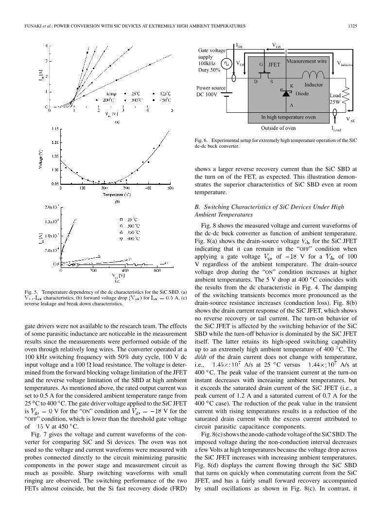
C. DC Characteristics of the SiC SBD
Fig. 5(a) illustrates the characteristics of the SiCSBD for different ambient temperatures. The cut-in voltage ofthe diode decreases with rising temperatures due to the Schottkybarrier height reduction with increasing temperature. The slopeof the linear region of the characteristic curve, which residesin the region higher than the cut-in voltage, becomes shallower
1324 IEEE TRANSACTIONS ON POWER ELECTRONICS, VOL. 22, NO. 4, JULY 2007
Fig. 3. DC characteristics of the SiC JFET for ambient temperatures as func-tion of V . (a) 25 C (Room temperature), (b) 200 C, (c) 450 C, (d) forwardblocking capability of SiC JFET for V = �20 V.
with rising temperatures. This means that the series resistancein the diode increases with rising temperatures.
Fig. 5(b) shows the forward voltage drop of the SiC SBDas function of temperature for . The forwardvoltage drop changes nonlinearly due to the adverse effectsof the cut-in voltage and series resistance changes with risingtemperatures. However, these forward voltage drop changesare relatively small when compared to the absolute value ofthe forward voltage drop, and the variation with temperature is
Fig. 4. Temperature dependency of the dc characteristics of the SiC JFET forthe “ON” condition. (a) V -I characteristics for V = 0 V, (b) saturationcurrent I for V = 20 V, (c) drain-source resistance for I = 0:5 A.
much smaller than that of the SiC JFET. Fig. 5(c) shows that thereverse leakage current of the SiC SBD increases significantlywhen the temperature exceeds 300 C. The reverse voltagecapability decreases from 660 V at 25 C to 100 V at 400C. This is very important for the designer because the SBD
is subjected to a reverse voltage equal to the converter inputvoltage.
IV. DC-DC BUCK CONVERTER OPERATION UNDER
HIGH TEMPERATURE CONDITIONS
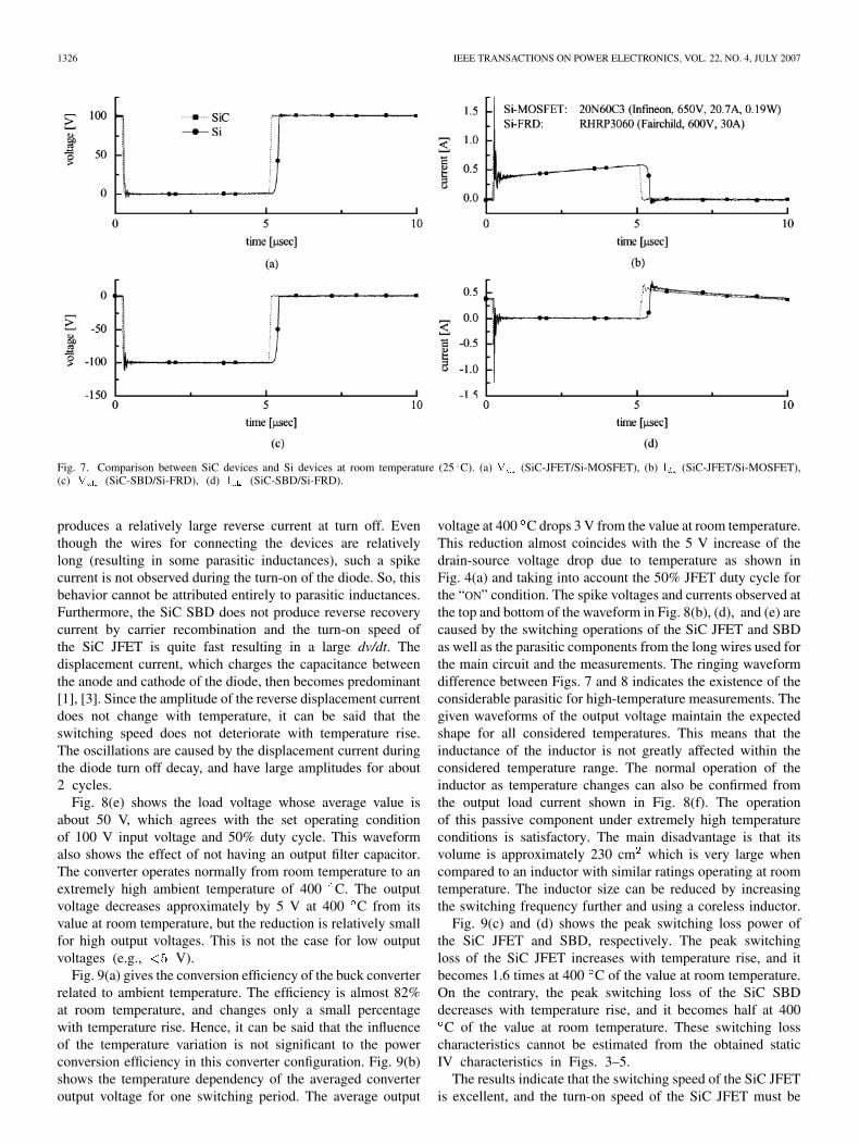
A. Experimental Setup
Fig. 6 illustrates the experimental setup for measuring theperformance of the SiC-based dc-dc buck converter. Only theSiC JFET, SBD and inductor are exposed to ambient tempera-ture variations in the oven since high-temperature capacitors and
FUNAKI et al.: POWER CONVERSION WITH SIC DEVICES AT EXTREMELY HIGH AMBIENT TEMPERATURES 1325
Fig. 5. Temperature dependency of the dc characteristics for the SiC SBD. (a)V -I characteristics, (b) forward voltage drop (V ) for I = 0:5 A, (c)reverse leakage and break down characteristics.
gate drivers were not available to the research team. The effectsof some parasitic inductance are noticeable in the measurementresults since the measurements were performed outside of theoven through relatively long wires. The converter operated at a100 kHz switching frequency with 50% duty cycle, 100 V dcinput voltage and a 100 load resistance. The voltage is deter-mined from the forward blocking voltage limitation of the JFETand the reverse voltage limitation of the SBD at high ambienttemperatures. As mentioned above, the rated output current wasset to 0.5 A for the considered ambient temperature range from25 C to 400 C. The gate driver voltage applied to the SiC JFETis V for the “ON” condition and V for the“OFF” condition, which is lower than the threshold gate voltageof V at 450 C.
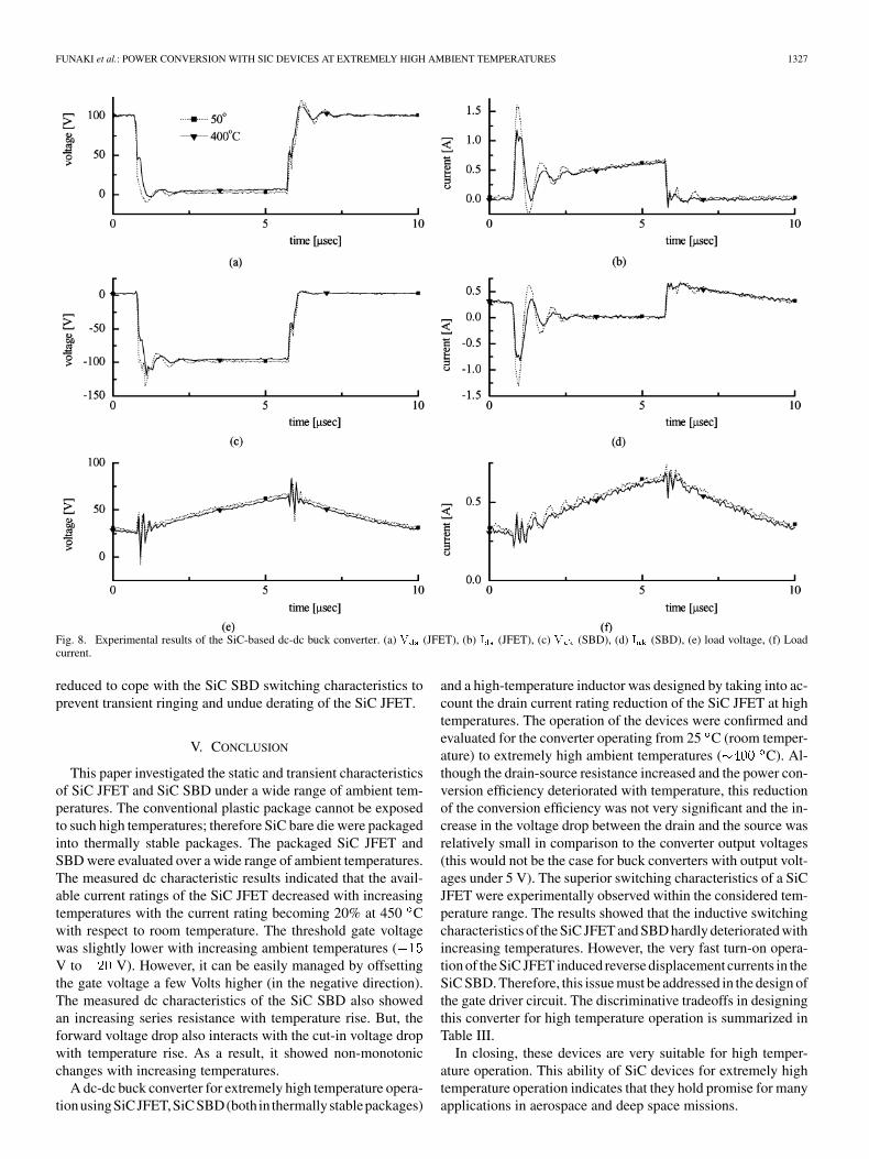
Fig. 7 gives the voltage and current waveforms of the con-verter for comparing SiC and Si devices. The oven was notused so the voltage and current waveforms were measured withprobes connected directly to the circuit minimizing parasiticcomponents in the power stage and measurement circuit asmuch as possible. Sharp switching waveforms with smallringing are observed. The switching performance of the twoFETs almost coincide, but the Si fast recovery diode (FRD)
Fig. 6. Experimental setup for extremely high temperature operation of the SiCdc-dc buck converter.
shows a larger reverse recovery current than the SiC SBD atthe turn on of the FET, as expected. This illustration demon-strates the superior characteristics of SiC SBD even at roomtemperature.
B. Switching Characteristics of SiC Devices Under HighAmbient Temperatures
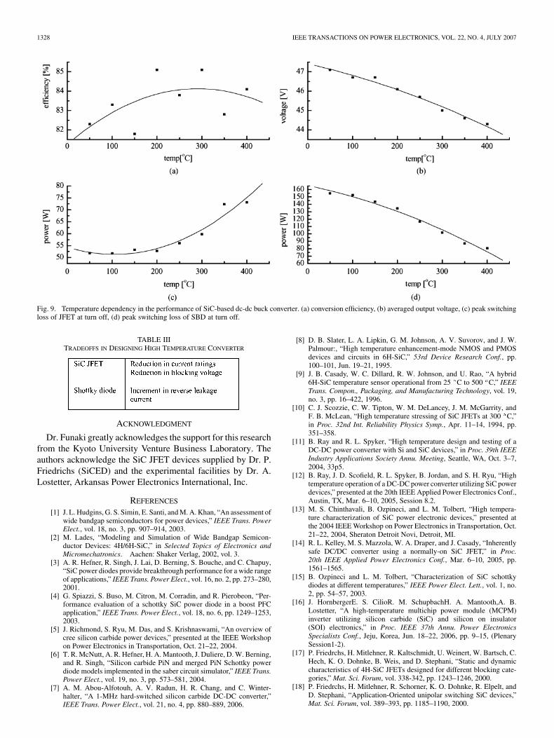
Fig. 8 shows the measured voltage and current waveforms ofthe dc-dc buck converter as function of ambient temperature.Fig. 8(a) shows the drain-source voltage for the SiC JFETindicating that it can remain in the “OFF” condition whenapplying a gate voltage of V for a of 100V regardless of the ambient temperature. The drain-sourcevoltage drop during the “ON” condition increases at higherambient temperatures. The 5 V drop at 400 C coincides withthe results from the dc characteristic in Fig. 4. The dampingof the switching transients becomes more pronounced as thedrain-source resistance increases (conduction loss). Fig. 8(b)shows the drain current response of the SiC JFET, which showsno reverse recovery or tail current. The turn-on behavior ofthe SiC JFET is affected by the switching behavior of the SiCSBD while the turn-off behavior is dominated by the SiC JFETitself. The latter retains its high-speed switching capabilityup to an extremely high ambient temperature of 400 C. Thedi/dt of the drain current does not change with temperature,i.e., A/s at 25 C versus A/s at400 C. The peak value of the transient current at the turn-oninstant decreases with increasing ambient temperatures, butit exceeds the saturated drain current of the SiC JFET (i.e., apeak current of 1.2 A and a saturated current of 0.7 A for the400 C case). The reduction of the peak value in the transientcurrent with rising temperatures results in a reduction of thesaturated drain current with the excess current attributed tocircuit parasitic capacitance components.
Fig. 8(c) shows the anode-cathode voltageof the SiC SBD.Theimposed voltage during the non-conduction interval decreasesa few Volts at high temperatures because the voltage drop acrossthe SiC JFET increases with increasing ambient temperatures.Fig. 8(d) displays the current flowing through the SiC SBDthat turns on quickly when commutating current from the SiCJFET, and has a fairly small forward recovery accompaniedby small oscillations as shown in Fig. 8(c). In contrast, it
1326 IEEE TRANSACTIONS ON POWER ELECTRONICS, VOL. 22, NO. 4, JULY 2007
Fig. 7. Comparison between SiC devices and Si devices at room temperature (25 C). (a) V (SiC-JFET/Si-MOSFET), (b) I (SiC-JFET/Si-MOSFET),(c) V (SiC-SBD/Si-FRD), (d) I (SiC-SBD/Si-FRD).
produces a relatively large reverse current at turn off. Eventhough the wires for connecting the devices are relativelylong (resulting in some parasitic inductances), such a spikecurrent is not observed during the turn-on of the diode. So, thisbehavior cannot be attributed entirely to parasitic inductances.Furthermore, the SiC SBD does not produce reverse recoverycurrent by carrier recombination and the turn-on speed ofthe SiC JFET is quite fast resulting in a large dv/dt. Thedisplacement current, which charges the capacitance betweenthe anode and cathode of the diode, then becomes predominant[1], [3]. Since the amplitude of the reverse displacement currentdoes not change with temperature, it can be said that theswitching speed does not deteriorate with temperature rise.The oscillations are caused by the displacement current duringthe diode turn off decay, and have large amplitudes for about2 cycles.
Fig. 8(e) shows the load voltage whose average value isabout 50 V, which agrees with the set operating conditionof 100 V input voltage and 50% duty cycle. This waveformalso shows the effect of not having an output filter capacitor.The converter operates normally from room temperature to anextremely high ambient temperature of 400 C. The outputvoltage decreases approximately by 5 V at 400 C from itsvalue at room temperature, but the reduction is relatively smallfor high output voltages. This is not the case for low outputvoltages (e.g., V).
Fig. 9(a) gives the conversion efficiency of the buck converterrelated to ambient temperature. The efficiency is almost 82%at room temperature, and changes only a small percentagewith temperature rise. Hence, it can be said that the influenceof the temperature variation is not significant to the powerconversion efficiency in this converter configuration. Fig. 9(b)shows the temperature dependency of the averaged converteroutput voltage for one switching period. The average output
voltage at 400 C drops 3 V from the value at room temperature.This reduction almost coincides with the 5 V increase of thedrain-source voltage drop due to temperature as shown inFig. 4(a) and taking into account the 50% JFET duty cycle forthe “ON” condition. The spike voltages and currents observed atthe top and bottom of the waveform in Fig. 8(b), (d), and (e) arecaused by the switching operations of the SiC JFET and SBDas well as the parasitic components from the long wires used forthe main circuit and the measurements. The ringing waveformdifference between Figs. 7 and 8 indicates the existence of theconsiderable parasitic for high-temperature measurements. Thegiven waveforms of the output voltage maintain the expectedshape for all considered temperatures. This means that theinductance of the inductor is not greatly affected within theconsidered temperature range. The normal operation of theinductor as temperature changes can also be confirmed fromthe output load current shown in Fig. 8(f). The operationof this passive component under extremely high temperatureconditions is satisfactory. The main disadvantage is that itsvolume is approximately 230 cm which is very large whencompared to an inductor with similar ratings operating at roomtemperature. The inductor size can be reduced by increasingthe switching frequency further and using a coreless inductor.
Fig. 9(c) and (d) shows the peak switching loss power ofthe SiC JFET and SBD, respectively. The peak switchingloss of the SiC JFET increases with temperature rise, and itbecomes 1.6 times at 400 C of the value at room temperature.On the contrary, the peak switching loss of the SiC SBDdecreases with temperature rise, and it becomes half at 400C of the value at room temperature. These switching loss
characteristics cannot be estimated from the obtained staticIV characteristics in Figs. 3–5.
The results indicate that the switching speed of the SiC JFETis excellent, and the turn-on speed of the SiC JFET must be
FUNAKI et al.: POWER CONVERSION WITH SIC DEVICES AT EXTREMELY HIGH AMBIENT TEMPERATURES 1327
Fig. 8. Experimental results of the SiC-based dc-dc buck converter. (a) V (JFET), (b) I (JFET), (c) V (SBD), (d) I (SBD), (e) load voltage, (f) Loadcurrent.
reduced to cope with the SiC SBD switching characteristics toprevent transient ringing and undue derating of the SiC JFET.
V. CONCLUSION
This paper investigated the static and transient characteristicsof SiC JFET and SiC SBD under a wide range of ambient tem-peratures. The conventional plastic package cannot be exposedto such high temperatures; therefore SiC bare die were packagedinto thermally stable packages. The packaged SiC JFET andSBD were evaluated over a wide range of ambient temperatures.The measured dc characteristic results indicated that the avail-able current ratings of the SiC JFET decreased with increasingtemperatures with the current rating becoming 20% at 450 Cwith respect to room temperature. The threshold gate voltagewas slightly lower with increasing ambient temperatures (V to V). However, it can be easily managed by offsettingthe gate voltage a few Volts higher (in the negative direction).The measured dc characteristics of the SiC SBD also showedan increasing series resistance with temperature rise. But, theforward voltage drop also interacts with the cut-in voltage dropwith temperature rise. As a result, it showed non-monotonicchanges with increasing temperatures.
A dc-dc buck converter for extremely high temperature opera-tionusingSiCJFET,SiCSBD(both in thermallystablepackages)
and a high-temperature inductor was designed by taking into ac-count the drain current rating reduction of the SiC JFET at hightemperatures. The operation of the devices were confirmed andevaluated for the converter operating from 25 C (room temper-ature) to extremely high ambient temperatures ( C). Al-though the drain-source resistance increased and the power con-version efficiency deteriorated with temperature, this reductionof the conversion efficiency was not very significant and the in-crease in the voltage drop between the drain and the source wasrelatively small in comparison to the converter output voltages(this would not be the case for buck converters with output volt-ages under 5 V). The superior switching characteristics of a SiCJFET were experimentally observed within the considered tem-perature range. The results showed that the inductive switchingcharacteristics of the SiC JFET and SBD hardly deteriorated withincreasing temperatures. However, the very fast turn-on opera-tion of the SiC JFET induced reverse displacement currents in theSiC SBD. Therefore, this issue must be addressed in the design ofthe gate driver circuit. The discriminative tradeoffs in designingthis converter for high temperature operation is summarized inTable III.
In closing, these devices are very suitable for high temper-ature operation. This ability of SiC devices for extremely hightemperature operation indicates that they hold promise for manyapplications in aerospace and deep space missions.
1328 IEEE TRANSACTIONS ON POWER ELECTRONICS, VOL. 22, NO. 4, JULY 2007
Fig. 9. Temperature dependency in the performance of SiC-based dc-dc buck converter. (a) conversion efficiency, (b) averaged output voltage, (c) peak switchingloss of JFET at turn off, (d) peak switching loss of SBD at turn off.
TABLE IIITRADEOFFS IN DESIGNING HIGH TEMPERATURE CONVERTER
ACKNOWLEDGMENT
Dr. Funaki greatly acknowledges the support for this researchfrom the Kyoto University Venture Business Laboratory. Theauthors acknowledge the SiC JFET devices supplied by Dr. P.Friedrichs (SiCED) and the experimental facilities by Dr. A.Lostetter, Arkansas Power Electronics International, Inc.
REFERENCES
[1] J. L. Hudgins, G. S. Simin, E. Santi, and M. A. Khan, “An assessment ofwide bandgap semiconductors for power devices,” IEEE Trans. PowerElect., vol. 18, no. 3, pp. 907–914, 2003.
[2] M. Lades, “Modeling and Simulation of Wide Bandgap Semicon-ductor Devices: 4H/6H-SiC,” in Selected Topics of Electronics andMicromechatronics. Aachen: Shaker Verlag, 2002, vol. 3.
[3] A. R. Hefner, R. Singh, J. Lai, D. Berning, S. Bouche, and C. Chapuy,“SiC power diodes provide breakthrough performance for a wide rangeof applications,” IEEE Trans. Power Elect., vol. 16, no. 2, pp. 273–280,2001.
[4] G. Spiazzi, S. Buso, M. Citron, M. Corradin, and R. Pierobeon, “Per-formance evaluation of a schottky SiC power diode in a boost PFCapplication,” IEEE Trans. Power Elect., vol. 18, no. 6, pp. 1249–1253,2003.
[5] J. Richmond, S. Ryu, M. Das, and S. Krishnaswami, “An overview ofcree silicon carbide power devices,” presented at the IEEE Workshopon Power Electronics in Transportation, Oct. 21–22, 2004.
[6] T. R. McNutt, A. R. Hefner, H. A. Mantooth, J. Duliere, D. W. Berning,and R. Singh, “Silicon carbide PiN and merged PiN Schottky powerdiode models implemented in the saber circuit simulator,” IEEE Trans.Power Elect., vol. 19, no. 3, pp. 573–581, 2004.
[7] A. M. Abou-Alfotouh, A. V. Radun, H. R. Chang, and C. Winter-halter, “A 1-MHz hard-switched silicon carbide DC-DC converter,”IEEE Trans. Power Elect., vol. 21, no. 4, pp. 880–889, 2006.
[8] D. B. Slater, L. A. Lipkin, G. M. Johnson, A. V. Suvorov, and J. W.Palmour:, “High temperature enhancement-mode NMOS and PMOSdevices and circuits in 6H-SiC,” 53rd Device Research Conf., pp.100–101, Jun. 19–21, 1995.
[9] J. B. Casady, W. C. Dillard, R. W. Johnson, and U. Rao, “A hybrid6H-SiC temperature sensor operational from 25 C to 500 C,” IEEETrans. Compon., Packaging, and Manufacturing Technology, vol. 19,no. 3, pp. 16–422, 1996.
[10] C. J. Scozzie, C. W. Tipton, W. M. DeLancey, J. M. McGarrity, andF. B. McLean, “High temperature stressing of SiC JFETs at 300 C,”in Proc. 32nd Int. Reliability Physics Symp., Apr. 11–14, 1994, pp.351–358.
[11] B. Ray and R. L. Spyker, “High temperature design and testing of aDC-DC power converter with Si and SiC devices,” in Proc. 39th IEEEIndustry Applications Society Annu. Meeting, Seattle, WA, Oct. 3–7,2004, 33p5.
[12] B. Ray, J. D. Scofield, R. L. Spyker, B. Jordan, and S. H. Ryu, “Hightemperature operation of a DC-DC power converter utilizing SiC powerdevices,” presented at the 20th IEEE Applied Power Electronics Conf.,Austin, TX, Mar. 6–10, 2005, Session 8.2.
[13] M. S. Chinthavali, B. Ozpineci, and L. M. Tolbert, “High tempera-ture characterization of SiC power electronic devices,” presented atthe 2004 IEEE Workshop on Power Electronics in Transportation, Oct.21–22, 2004, Sheraton Detroit Novi, Detroit, MI.
[14] R. L. Kelley, M. S. Mazzola, W. A. Draper, and J. Casady, “Inherentlysafe DC/DC converter using a normally-on SiC JFET,” in Proc.20th IEEE Applied Power Electronics Conf., Mar. 6–10, 2005, pp.1561–1565.
[15] B. Ozpineci and L. M. Tolbert, “Characterization of SiC schottkydiodes at different temperatures,” IEEE Power Elect. Lett., vol. 1, no.2, pp. 54–57, 2003.
[16] J. HornbergerE. S. CilioR. M. SchupbachH. A. Mantooth,A. B.Lostetter, “A high-temperature multichip power module (MCPM)inverter utilizing silicon carbide (SiC) and silicon on insulator(SOI) electronics,” in Proc. IEEE 37th Annu. Power ElectronicsSpecialists Conf., Jeju, Korea, Jun. 18–22, 2006, pp. 9–15, (PlenarySession1-2).
[17] P. Friedrchs, H. Mitlehner, R. Kaltschmidt, U. Weinert, W. Bartsch, C.Hech, K. O. Dohnke, B. Weis, and D. Stephani, “Static and dynamiccharacteristics of 4H-SiC JFETs designed for different blocking cate-gories,” Mat. Sci. Forum, vol. 338-342, pp. 1243–1246, 2000.
[18] P. Friedrchs, H. Mitlehner, R. Schorner, K. O. Dohnke, R. Elpelt, andD. Stephani, “Application-Oriented unipolar switching SiC devices,”Mat. Sci. Forum, vol. 389–393, pp. 1185–1190, 2000.
FUNAKI et al.: POWER CONVERSION WITH SIC DEVICES AT EXTREMELY HIGH AMBIENT TEMPERATURES 1329
Tsuyoshi Funaki (M’00) received the B.E. and M.E. degrees in electrical en-gineering and the Ph.D. degree all from Osaka University, Osaka, Japan.
He joined Osaka University as an Research Associate in 1994 and became anAssistant Professor in 2001. In 2002, he joined Kyoto University, Kyoto, Japan,as an Associate Professor. He was a Visiting Scholar in the Electrical Engi-neering Department, University of Arkansas, Fayetteville, in 2004 and 2005,where he did collaborative research on SiC device and its application.
Dr. Funaki is a member of the Institute of Electrical Engineers of Japan(IEEJ), the Institute of Electronics, Information and Communication Engineers(IEICE) of Japan, the Institute of Systems, Control and Information Engineers(ISCIE), Society of Atmospheric Electricity of Japan (SAEJ), and the Institu-tion of Engineering and Technology (IET), London, U.K.
Juan Carlos Balda (M’78–SM’94) was born in Bahía Blanca, Argentina. He re-ceived the B.Sc. degree in electrical engineering from the Universidad Nacionaldel Sur, Bahía Blanca, Argentina, in 1979, and the Ph.D. degree in electricalengineering from the University of Natal, Durban, South Africa, in 1986.
In 1979, he worked for two and one-half years at Hidronor S.A., an electricutility in the Southwestern part of Argentina. He was employed as a Researcherand a part-time Lecturer at the University of Natal until July 1987. He then spenttwo years as a visiting Assistant Professor at Clemson University, Clemson, SC.He has been at the University of Arkansas, Fayetteville, since July 1989 wherehe is currently a Full Professor and Associate Department Head. His main re-search interests are power electronics, electric power distribution systems, motordrives and electric power quality.
Dr. Balda is a member of the Power Electronics and Industry ApplicationsSocieties, and the honor society Eta Kappa Nu. He is a counselor of the IEEEStudent branch and a Faculty Advisor to the Ham Radio Club at the Universityof Arkansas.
Jeremy Junghans (S’03-M’07) is currently pursuing the M.S.E.E. degree at theUniversity of Arkansas, Fayetteville.
He is currently working as the Principle Product, Packaging and AssemblyEngineer for the RF Power Devices Group at Northrop Grumman ElectronicSystems in Baltimore, MD. His responsibilities include modeling and simu-lation of packaged transistors, design of packaging layouts including internalmatching networks and oversight of production assembly of high frequencypower devices. His previous research includes the spray cooling of power elec-tronics, fabrication and packaging of silicon carbide (SiC) devices and the pro-duction of multilayer circuits using low temperature cofired ceramics (LTCC).
Mr. Junghans previously served as the Vice-President of the IEEE CPMT So-ciety and President of the International Microelectronics and Packaging Societystudent chapters.
Avinash S. Kashyap (S’03) was born in Thrissur, India, on October 14, 1979.He received the B.Tech degree in electrical and electronics engineering fromthe University of Calicut, India, in 2001 and the M.S. degree in electrical en-gineering from the University of Arkansas, Fayetteville, in 2005 where he iscurrently pursuing the Ph.D. degree in electrical engineering.
His research interests include the design, modeling and fabrication of siliconcarbide (SiC) devices. He has previously interned at the Oak Ridge NationalLaboratory’s wide bandgap research group at Knoxville, TN, and the SPICEmodeling group of National Semiconductor at Santa Clara, CA.
Mr. Kashyap is a recipient of the Sam Walton Doctoral Academy Fellowshipand the William E. Clark Endowed Doctoral Fellowship.
H. Alan Mantooth (S’83–M’90–SM’97) received the B.S. (summa cum laude)and M. S. degrees in electrical engineering from the University of Arkansas(UA), Fayetteville, in 1985 and 1987, respectively, and the Ph.D. degree fromthe Georgia Institute of Technology, Atlanta, in 1990.
He joined Analogy in 1990 where he focused on semiconductor device mod-eling and the research and development of HDL-based modeling tools and tech-niques. Besides modeling, his interests include analog and mixed-signal IC de-sign. In 1996, he was named a Distinguished Member of Technical Staff atAnalogy (now owned by Synopsys). In 1998, he joined the faculty of the De-partment of Electrical Engineering at the UA, as an Associate Professor and waspromoted to his present rank of Full Professor in 2002. In 2003, he co-founded
Lynguent, an EDA company focused on modeling and simulation tools. He es-tablished the National Center for Reliable Electric Power Transmission at theUA in 2005, for which he serves as Director. He has published over 100 articleson models, modeling techniques, and modeling strategies. He holds patents onsoftware architecture and algorithms for modeling tools and has others pending.He is coauthor of the book Modeling with an Analog Hardware Description Lan-guage (Kluwer Academic, 1995).
Dr. Mantooth is a member of Tau Beta Pi and Eta Kappa Nu. He was selectedto the Georgia Tech Council of Outstanding Young Engineering Alumni in 2002and has received a teaching, service, and/or research award every year since re-turning to the UA. In 2006, he was selected as the inaugural holder of the 21stCentury Chair in Mixed-Signal IC Design and CAD, an endowed chair position.He has served on several technical program committees for IEEE conferences.He was the Technical Program Chair for the IEEE International Workshop onBehavioral Modeling and Simulation (BMAS) in 2000 and General Chair in2001. He served as Guest Editor for a Special Issue on Behavioral Modelingand Simulation for the IEEE TRANSACTIONS ON COMPUTER-AIDED DESIGN inFebruary 2003 and as an IEEE Circuits and Systems Society Distinguished Lec-turer in 2003–2004. He is currently serving the profession in the following roles:1) IEEE CAS representative on the Design Automation Conference ExecutiveCommittee, 2) Member of the IEEE Council on Electronic Design Automation,and 3) Member of the Power Electronics Society Advisory Committee as Chairof the Society’s Standards Committee.
Fred Barlow (M’96) received the B.S. degree in physics and applied physicsfrom Emory University, Atlanta, GA and the M.Sc. and Ph.D. degrees in elec-trical engineering from the Virginia Polytechnic Institute and State University(Virginia Tech), Blacksburg.
He is currently working as an Associate Professor in the Electrical and Com-puter Engineering Department at the University of Idaho, Moscow, with an em-phasis on electronic packaging. He has published widely on electronic pack-aging and electronic materials evaluation and is a coeditor of The Handbook ofThin Film Technology (McGraw Hill, 1998), as well as the Handbook of Ce-ramic Interconnect Technology (CRC Press, 2007).
Dr. Barlow is a senior member of the International Microelectronics andPackaging Society (IMAPS). He also serves as the Editor-in-Chief of theJournal of Microelectronics and Electronic Packaging.
Tsunenobu Kimoto (M’00) received the B.E. and M.E. degrees in electricalengineering and the Ph.D. degree (based on his work on SiC epitaxial growth,material characterization, and high-voltage diodes) in 1996, all from Kyoto Uni-versity, Kyoto, Japan, in 1986, 1988, and 1996, respectively.
He joined Sumitomo Electric Industries, Ltd., in April 1988, where he con-ducted research on amorphous-Si solar cells and semiconducting diamond ma-terial for high-temperature devices. In 1990, he started SiC research work as aResearch Associate at Kyoto University. From September 1996 through August1997, he was a Visiting Scientist at Linköping University, Linköping, Sweden,where he was involved in fast epitaxy of SiC and high-voltage Schottky diodes.He is currently a Professor in the Department of Electronic Science and En-gineering, Kyoto University. He has published over 200 papers in scientificjournals and international conference proceedings. His main research activityincludes SiC epitaxial growth, optical and electrical characterization, ion im-plantation, MOS physics, and high-voltage diodes and transistors.
Takashi Hikihara (S’84-M’88) was born in Kyoto, Japan, in 1958. He receivedthe B.E. degree from Kyoto Institute of Technology, Kyoto, Japan, in 1982, andthe M.E., and Ph.D. degrees from Kyoto University, Kyoto, Japan, in 1984, and1990, respectively.
From 1987 to 1997, he was with the faculty of the Department of ElectricalEngineering, Kansai University, Osaka, Japan. From 1993 to 1994, he was aVisiting Researcher at Cornell University. In 1997, he joined the Departmentof Electrical Engineering, Kyoto University, American Physics Society (APS),Society for Industrial and Applied Mathematics (SIAM), and so on. where heis currently a Professor. His research interests include nonlinear science and itsapplication. He is also interested in system control and nanotechnology.
Dr. Hikihara is a member of the Institution of Engineering and Technology(IET), London, U.K., the Institute of Electronics, Information and Communica-tion Engineers (IEICE) of Japan, The Institute of Electrical Engineers of Japan(IEEJ), the American Physics Society (APS), the Society for Industrial and Ap-plied Mathematics (SIAM), and so on. He was an Associate Editor for the Trans-actions of the IEICE, the IEEJ, and others. He is currently an Associate Editorof the Journal of Circuits, Systems, and Computers.


![Chapter 2 SiC Materials and Processing Technology€¦ · 34 2 SiC Materials and Processing Technology Table 2.1 Key electrical parameters of SiC [1] Property 4H-SiC 6H-SiC 3C-SiC](https://img.pdfslide.us/doc/110x75/5f4fd11797ddad63bf719816/chapter-2-sic-materials-and-processing-technology-34-2-sic-materials-and-processing.jpg)