Embed Size (px)
Citation preview

Title: Performance Enhancement for LTE and
Beyond Systems
Name: Wei Li
This is a digitised version of a dissertation submitted to the University of Bedfordshire.
It is available to view only.
This item is subject to copyright.

Performance Enhancement for LTE
and Beyond Systems
Wei Li
Institute for Research in Applicable Computing
University of Bedfordshire
A thesis submitted to the University of Bedfordshire in
fulfilment of the requirements for the degree of
Doctor of Philosophy
September 2014
i
Abstract Wireless communication systems have undergone fast development in recent
years. Based on GSM/EDGE and UMTS/HSPA, the 3rd Generation Partnership
Project (3GPP) specified the Long Term Evolution (LTE) standard to cope with
rapidly increasing demands, including capacity, coverage, and data rate. To
achieve this goal, several key techniques have been adopted by LTE, such as
Multiple-Input and Multiple-Output (MIMO), Orthogonal Frequency-Division
Multiplexing (OFDM), and heterogeneous network (HetNet). However, there are
some inherent drawbacks regarding these techniques. Direct conversion
architecture is adopted to provide a simple, low cost transmitter solution. The
problem of I/Q imbalance arises due to the imperfection of circuit components;
the orthogonality of OFDM is vulnerable to carrier frequency offset (CFO) and
sampling frequency offset (SFO). The doubly selective channel can also severely
deteriorate the receiver performance. In addition, the deployment of
Heterogeneous Network (HetNet), which permits the co-existence of macro and
pico cells, incurs inter-cell interference for cell edge users. The impact of these
factors then results in significant degradation in relation to system performance.
This dissertation aims to investigate the key techniques which can be used to
mitigate the above problems. First, I/Q imbalance for the wideband transmitter is
studied and a self-IQ-demodulation based compensation scheme for frequency-
dependent (FD) I/Q imbalance is proposed. This combats the FD I/Q imbalance
by using the internal diode of the transmitter and a specially designed test signal
without any external calibration instruments or internal low-IF feedback path. The
instrument test results show that the proposed scheme can enhance signal quality
by 10 dB in terms of image rejection ratio (IRR).
In addition to the I/Q imbalance, the system suffers from CFO, SFO and
frequency-time selective channel. To mitigate this, a hybrid optimum OFDM
receiver with decision feedback equalizer (DFE) to cope with the CFO, SFO and
doubly selective channel. The algorithm firstly estimates the CFO and channel
frequency response (CFR) in the coarse estimation, with the help of hybrid

Abstract
ii
classical timing and frequency synchronization algorithms. Afterwards, a pilot-
aided polynomial interpolation channel estimation, combined with a low
complexity DFE scheme, based on minimum mean squared error (MMSE) criteria,
is developed to alleviate the impact of the residual SFO, CFO, and Doppler effect.
A subspace-based signal-to-noise ratio (SNR) estimation algorithm is proposed to
estimate the SNR in the doubly selective channel. This provides prior knowledge
for MMSE-DFE and automatic modulation and coding (AMC). Simulation results
show that this proposed estimation algorithm significantly improves the system
performance. In order to speed up algorithm verification process, an FPGA based
co-simulation is developed.
Inter-cell interference caused by the co-existence of macro and pico cells has a big
impact on system performance. Although an almost blank subframe (ABS) is
proposed to mitigate this problem, the residual control signal in the ABS still
inevitably causes interference. Hence, a cell-specific reference signal (CRS)
interference cancellation algorithm, utilizing the information in the ABS, is
proposed. First, the timing and carrier frequency offset of the interference signal is
compensated by utilizing the cross-correlation properties of the synchronization
signal. Afterwards, the reference signal is generated locally and channel response
is estimated by making use of channel statistics. Then, the interference signal is
reconstructed based on the previous estimate of the channel, timing and carrier
frequency offset. The interference is mitigated by subtracting the estimation of the
interference signal and LLR puncturing. The block error rate (BLER) performance
of the signal is notably improved by this algorithm, according to the simulation
results of different channel scenarios.
The proposed techniques provide low cost, low complexity solutions for LTE and
beyond systems. The simulation and measurements show good overall system
performance can be achieved.

iii
Acknowledgements
Firstly, I would like to thank my supervisor, Dr. Yue Zhang and Dr. Vladimir
Dyo, for their guidance and invaluable comments. I would also like to thank
Professor Edmond C. Prakash and Dr. Dayou Li for their advice during my
research period in Bedfordshire. Special thanks goes to Dr. Li-Ke Huang, Dr.
Hong Wei and Kexuan Sun for their valuable input into discussions, and
suggestions, relating to my thesis.
The financial support for this work was provided by Aeroflex Ltd. as part of
their student research program and this is hereby acknowledged.
Finally, I would like to express my gratitude to my parents and brother for their
inexhaustible love, support and encouragement.
Contents
iv
Contents
Abstract .................................................................................................................... i Acknowledgements ................................................................................................ iii List of Figures ........................................................................................................ vi List of Tables ....................................................................................................... viii Abbreviations ......................................................................................................... ix 1. Introduction ....................................................................................................... 1
1.1 Research background .............................................................................. 1 1.2 Research problem ................................................................................... 5
1.2.1 I/Q imbalance ............................................................................... 6 1.2.2 Receiver algorithm ..................................................................... 10
1.3 Objectives and solution approach ......................................................... 13 1.4 Outline of the thesis .............................................................................. 16 1.5 Main contributions ................................................................................ 18 1.6 Papers published and submitted ........................................................... 19
2. Physical Layer Model of LTE and Beyond Systems ...................................... 21 2.1 Introduction .......................................................................................... 21 2.2 Transceiver impairments ...................................................................... 23 2.3 Wireless channel model ........................................................................ 25
2.3.1 Wireless channel environment ................................................... 26 2.4 OFDM signal model ............................................................................. 27 2.5 LTE PHY standards and eICIC ............................................................ 33
2.5.1 LTE downlink PHY data processing.......................................... 36 2.5.2 LTE downlink frame structure and radio resource .................... 37 2.5.3 Key LTE downlink physical signals .......................................... 39 2.5.4 LTE eICIC scheme ..................................................................... 40
3. Self-IQ-demodulation based FD I/Q Imbalance Compensation ..................... 42 3.1 Introduction .......................................................................................... 42 3.2 I/Q Imbalance model ............................................................................ 45
3.2.1 Ideal quadrature modulation ...................................................... 45 3.2.2 Quadrature modulation with IQ imbalance ................................ 47
3.3 Conventional I/Q imbalance estimation methods ................................. 54 3.3.1 Diode based estimation methods ................................................ 54 3.3.2 LOW-IF based estimation methods ........................................... 57
3.4 Proposed I/Q imbalance estimation method ......................................... 61 3.4.1 LO impairments and DC offset estimation ................................ 64 3.4.2 FD related I/Q impairment parameters estimation ..................... 69 3.4.3 Inphase demodulation for inphase branch signal ....................... 70 3.4.4 Quadrature demodulation for inphase branch signal ................. 72 3.4.5 Inphase demodulation for quadrature branch signal .................. 74 3.4.6 Quadrature demodulation of signal from Q branch ................... 75
3.5 Frequency I/Q imbalance pre-distortion technique .............................. 78 3.6 Simulation and laboratory experiment results ...................................... 79
3.6.1 Simulation and laboratory experiment settings .......................... 79 3.6.2 Estimation of LO impairments ................................................... 80 3.6.3 Estimation of overall I/Q imbalance .......................................... 82

Contents
v
3.6.4 Effect of higher order intermodulation and multi-tone .............. 85 3.7 Conclusions .......................................................................................... 88
4. MMSE-DFE based OFDM Receiver Algorithm............................................. 89 4.1 Introduction .......................................................................................... 89 4.2 Impact of impairments .......................................................................... 92
4.2.1 Impact of STO ............................................................................ 92 4.2.2 Impact of CFO ........................................................................... 94 4.2.3 Impact of SFO ............................................................................ 95
4.3 Receiver algorithm ............................................................................... 97 4.3.1 Timing synchronization and coarse estimation .......................... 97 4.3.2 Fine estimation ......................................................................... 100
4.4 Co-simulation platform ....................................................................... 108 4.5 Simulation results ............................................................................... 111 4.6 Conclusion .......................................................................................... 117
5. Subspace-based noise estimation .................................................................. 119 5.1 Introduction ........................................................................................ 119 5.2 System model ..................................................................................... 120
5.2.1 Applicable pilot scenarios ........................................................ 120 5.3 System model ..................................................................................... 121
5.3.1 Conventional moving average method..................................... 122 5.3.2 Proposed subspace-based SNR estimation algorithm .............. 124
5.4 Simulation results ............................................................................... 130 5.5 Conclusion .......................................................................................... 135
6. Robust CRS interference cancellation .......................................................... 136 6.1 Introduction ........................................................................................ 136 6.2 Interference analysis and model ......................................................... 138 6.3 Interference cancellation algorithm .................................................... 141
6.3.1 TO/CFO estimation .................................................................. 142 6.3.2 Interfering channel estimation.................................................. 144 6.3.3 Interfering signal reconstruction and reduction ....................... 148 6.3.4 LLR scaling .............................................................................. 148
6.4 Simulation results ............................................................................... 149 6.5 Conclusion .......................................................................................... 156
7. Conclusions ................................................................................................... 157 7.1 Discussions ......................................................................................... 157 7.2 Further work ....................................................................................... 159
Reference.............................................................................................................. 161 Appedix A: The Effect of Resampler................................................................... 173 Appedix B: The Effect of Resampler to EVM of OFDM Signal ......................... 173

List of Figures
vi
List of Figures
Figure 1.1 The Evolution of Wireless Communication Systems .................... 5 Figure 1.2 Typical LTE Network. ................................................................... 6 Figure 1.3 Frequency Response of FD and FI IQ Imbalance ......................... 7 Figure 2.1 LTE Network Topology .............................................................. 22 Figure 2.2 Direct Conversion Transmitter and Receiver Model ................... 24 Figure 2.3 Propagation of Radio Signal in Wireless Channel ...................... 26 Figure 2.4 Subcarriers in FDM Systems ....................................................... 28 Figure 2.5 Subcarriers in OFDM Systems .................................................... 29 Figure 2.6 Cyclic Prefix in OFDM ............................................................... 31 Figure 2.7 Brief Illustration of OFDM and OFDMA ................................... 34 Figure 2.8 Three MIMO Techniques in LTE ................................................ 35 Figure 2.9 LTE Downlink PHY Data Processing ......................................... 37 Figure 2.10 Structure for Type 1 Frames ...................................................... 37 Figure 2.11 Structure of Resource Grid and Resource Block ....................... 39 Figure 2.12 Heterogeneous Network ............................................................ 41 Figure 2.13 Basic Principle of ABS .............................................................. 41 Figure 3.1Proposed Compensation Scheme .................................................. 45 Figure 3.2 Ideal DCT Topology .................................................................... 45 Figure 3.3 Ideal DCT Spectrum Transfer ..................................................... 47 Figure 3.4 Practical DCT Architecture with I/Q Imbalance Imperfections .. 48 Figure 3.5 Signal Spectrum for Ideal and Practical DCT ............................. 54 Figure 3.6 Transmitter with Diode-based Feedback path ............................. 55 Figure 3.7 IQ Imbalance Estimation in Literature [22] ................................. 56 Figure 3.8 Transmitter with Low-IF Receiver Feedback Path ...................... 58 Figure 3.9 Proposed Estimation Architecture ............................................... 62 Figure 3.10 I/Q demodulation ....................................................................... 63 Figure 3.11Frequency-dependent I/Q Imbalance Estimation Procedure ...... 64 Figure 3.12 Signal Spectrum Transfer for Step a and b ................................ 68 Figure 3.13 Amplitude of and Calculated from Derivation and
Simulations ............................................................................................ 69 Figure 3.14 Self-I/Q-demodulation based Estimation Process ..................... 78 Figure 3.15 Transmitter I/Q imbalance Pre-distorter .................................... 79 Figure 3.16 Laboratory Experiment Configuration ...................................... 80 Figure 3.17 LO Imbalance Calibration Performance .................................... 82 Figure 3.18 Calibration performance at .................................... 84 Figure 3.19 Compensation performance with varies from 5 to 75 MHz .. 85 Figure 3.20 Effect of Diode Higher Order intermodulation and Different
Numbers of Tones ................................................................................. 86 Figure 3.21 Effect of Different Transmission power .................................... 86 Figure 4.1 STO Impact on FFT Window ...................................................... 93 Figure 4.2 CFO Induced SNR Loss .............................................................. 95 Figure 4.3 Shifted FFT Window ................................................................... 96 Figure 4.4 The Phase Rotation caused by SFO ............................................. 97 Figure 4.5 System Diagram for Hybrid Pilot-aided channel Estimation ...... 97

List of Figures
vii
Figure 4.6 DFE Diagram ............................................................................. 103 Figure 4.7 Algorithm Verification Flow ..................................................... 109 Figure 4.8 UDP Packets Transmission ....................................................... 110 Figure 4.9 System Diagram of Co-simulation Platform ............................. 111 Figure 4.10 NMSE of CFO Estimation V.S. Varying SNRs for different
CFOs ................................................................................................... 113 Figure 4.11 NMSE of Channel Estimation for Different SFO and Doppler
Shifts ................................................................................................... 114 Figure 4.12 EVM Performance comparisons for SFO Estimator and
Preceding Parts .................................................................................... 115 Figure 4.13 EVM Comparison between DFE and Pre-DFE Parts ............. 116 Figure 4.14 Performance of Proposed DFE and Conventional DFE .......... 117 Figure 5.1 Pilot Pattern in One RB ............................................................. 121 Figure 5.2 Moving Average Based SNR Estimation .................................. 123 Figure 5.3 Moving Average SNR Estimation in Time Varying Fading. .... 124 Figure 5.4 Proposed SNR estimation process ............................................. 125 Figure 5.5 Proposed Subspace-based SNR Estimation ............................... 130 Figure 5.6 Laboratory Testbench Configuration ......................................... 131 Figure 5.7 SNR NMSE v.s. SNR for Different Channels ........................... 132 Figure 5.8 SNR Estimation Result with Different Pilot in PXI Modules ... 133 Figure 5.9 Emulation Results for Subspace-based Noise Variance Estimation
............................................................................................................. 134 Figure 5.10 Comparison of Different SNR Estimation Methods ................ 135 Figure 6.1 Inter-cell Interference between Macro and Pico Cell ................ 138 Figure 6.2 Received signal in time and frequency grid .............................. 139 Figure 6.3 CRS Interference Cancellation Receiver Architecture .............. 142 Figure 6.4 Synchronization Signal .............................................................. 144 Figure 6.5 BLER performance versus SNR in dfferent IC scenario ........... 152 Figure 6.6 BLER Performance of Different Doppler Frequency Scenarios 153 Figure 6.7 Effect of Average Window Length ............................................ 154 Figure 6.8 BLER Performance vs. Frequency Offset ................................. 155 Figure 6.9 BLER Performance vs. Timing Offset ...................................... 155

viii
List of Tables
Table 3.1 “time division” I/Q Demodulation Process ................................... 70 Table 3.2 Measured IRR Before and After Compensation for Different and
in ................................................................................................ 82 Table 4.1 Hardware Consumption of Some Important FGPA Modules ..... 111 Table 5.1 Estimation Results of MDL Method ........................................... 128 Table 5.2 Estimation Results of MDL and Modified MDL ........................ 129 Table 5.3 Important Simulation Parameters................................................ 131 Table 6.1 Key Simulation Parameters ......................................................... 150

Abbreviation
ix
Abbreviations
3GPP 3rd Generation Partnership Project
ABS Almost Blank Subframe
AMC Adaptive Modulation and Coding
AWGN Additive White Gaussian Noise
BLER Block Error Rate
CDMA Code Division Multiple Access
CIR Channel Impulse Response
CoMP Coordinated Multipoint Transmission
CP Cyclic Prefix
CQI Channel Quality Indicator
CRS Cell Specific Reference Signal
DAC Digital-to-Analog Convert
DCI Downlink Control Information
DCT Direct conversion transmitter
DFE Decision feedback equalizer
DSP Digital Signal Processing
EDGE Enhanced Data rates for GSM Evolution
EPA Extended Pedestrian A model
ETU Extended Typical Urban model
EVA Extended Vehicular A model
eICIC Enhanced Inter Cell Interference Coordination
FD Frequency-Dependent
FDD Frequency-Division Duplexing
FDM Frequency Division Multiplexing
FDMA Frequency division multiple access
FEC Forward Error Correction
FeICIC Further eICIC
FI Frequency-Independent
FM Frequency modulation
GI Guard Interval

Abbreviation
x
GPRS General Packet Radio Service
GSM Global System for Mobile
HetNet Heterogeneous Network
HSPA High Speed Packet Access
ICI Inter-Carrier Interference
IF Intermediate Frequency
IFFT Inverse Fast Fourier Transform
IRR Image Rejection Ratio
ISI Inter-Symbol Interference
LLR Log-Likelihood Ratio
LO Local oscillator
LPF Lowpass Filter
LTE Long term Evolution
MAC Media Access Control
MIMO Multiple-Input and Multiple-Output
OFDM Orthogonal Frequency-Division Multiplexing
OFDMA Orthogonal Frequency-Division Multiple Access
SNR Signal-to-Noise Ratio
SSS Secondary Syncrhonization Signal
STO Symbol Timing Offset
PAR Peak-to-Average Ratio
PBCH Physical Broadcast Channel
PCFICH Physical Control Format Indicator Channel
PCH Physical Channel
PDCCH Physical Downlink Control Channel
PDCP Packet data Convergence Protocol
PDF Probability Density Function
PDP Power Delay Profile
PDSCH Physical Downlink Shared Channel
PHICH Physical Hybrid ARQ Indicator Channel
PHY Physical Layer
PMCH Physical Multicast Channel

Abbreviation
xi
PMI Precoding Matrix Indicator
PSD Power Spectrum Density
PSS Primary Synchronization Signal
QAM Quadrature amplitude modulation
RAN Radio Access Network
RCL Radio Link Control
RB Resource Block
RE Resource Element
RI Rank Indicator
RRC Radio Resource Control
SINR Signal-to-Interference plus Noise Ratio
SNR Signal-to-Noise Ratio
STBC Space-Time Block Coding
TB Transport Block
TDD Time-Division Duplexing
TDL Tapped Delay Line
TTI Transmission Time Interval
UE User Equipment
UMTS Universal Mobile Telecommunications System
WLAN Wireless Local Area Network
W-CDMA Wideband Code Division Multiple Access

1
1. Introduction
1.1 Research background
Due to the rapid development of hardware and signal processing theory, the last
few years have witnessed a tremendous growth in the wireless communication
industry. The amount of mobile users was 6.62 billion globally in 2013, and
ownership ratio of mobile handsets was 93.1%. In contrast to this, the figures in
2008 were, respectively, 4.1 billion and 61% [1]. In addition, there is a clear trend
implying fixed-communication will shift to mobile communication.
The inherent motivation for this trend can be attributed to a variety of factors.
Because of the development of the very-large-scale integration circuits (VLSI),
hardware is much more powerful in terms of computation capability, noise
performance, and dynamic range, which enables hardware platforms to support
much higher transmission data rates, signal bandwidth, transmission power, and
receiver sensitivity. In addition, improvements in electronics technology have
provided lower cost, lower power consumption, and smaller sizes, which affords
electronic equipment users a much better mobility experience. On the other hand,
the increasing demand for ubiquitous access to networks in both stationary and
mobile scenarios has continuously required more sophisticated equipment. The
demand for higher data rates, and denser equipment also drives the development
of wirelss communication systems in the direction of high data throughput, and
better user experience. The development of wireless communication systems can
be divided into four stages, according to techniques and services:
First generation (1G): The first generation system began operation in the 1970s
and used analog transimssion for voice services. Different systems were deployed,
for example, NMT and TACS in Europe, and AMPS in North America. These
systems adopt techniques such as freqeuncy modulation (FM), directional

1. Introduction
2
antennas, handover and roaming and frequency division multiple access (FDMA)
which support data rate less that 100 kbps [2], [3].
Second generation (2G): The second generation system was launched at the
beginning of the 1980s. Compared with 1G, 2G systems are mostly based on
circuit-switched technology. The most popular 2G system is the Global System
for Mobile Communication (GSM), which makes use of spectrum resource by
splitting the frequency spectrum into several 200 KHz bandwidth channels. In
addition, GSM also adopts Time Division Multiple Access (TDMA), which
allows more users to access frequency resources. In addition to GSM technology
in Europe, Code Division Multiple Access (CDMA) technology was developed in
North America, which increased network capacity and provided clearer voice
quality. 2G has seen the introduction of General Packet Radio Service (GPRS)
and Enhanced Data rates for GSM Evolution (EDGE) to cope with the demand for
higher data rates and voice services. These technologies have enabled data rates to
reach 150 kbps and 384 kbps respectively [4].
Third Generation (3G): Aiming to provide a high speed data service, global
accessibility and high capacity, the International Telecommunication Union
defined International Mobile Telecommunications-2000 (IMT-2000) as 3G
technology. Due to reasons regarding different technical routes and business
policies, IMT-2000 has included a variety of systems in different areas: UMTS in
Europe, W-CDMA as the evolution of GSM, TD-SCDMA based on CDMA,
CDMA2000, and so forth. A variety of techniques are adopted in these systems
including adaptive modulation & coding (AMC), Orthogonal Transmit Diversity
(OTD), Space Time Spreading (STS), and virtual soft handoff. These techniques
result in a peak data rate of up to 2 Mbps for stationary users. An essential
definition of 3G is that it relates to different technologies and these technologies
are moving towards a converged worldwide network.
Fourth Generation (4G): 4G technology long term evolution (LTE) will try to
integrate almost every wireless standard in use and provide an enhanced user

1. Introduction
3
experience. In this system, the user will have ubiquitous access to the network and
multiple varieties of services at a low cost. Accordingly, the 3rd Generation
Partnership Project (3GPP) proposed some key requirements: data rate ranges
from 500-100 Mbps for high mobility users to Gbps for low mobility users;
mobility up to 350 km/h, scalable bandwidth and spectrum aggregation (Release
11) with bandwidths of more than 40 MHz. In order to achieve these goals, the
first LTE release (Release 8) adopted some key techniques including: Multi-input
and multiple-output (MIMO) antenna, Orthogonal Frequency-Division Multiple
Access (OFDMA) in downlink, inter-cell interference mitigation, Adaptive
Modulation and Coding (AMC) depending on radio link quality, and an all-IP
based network. The 4G network has been deployed all over the world and
provides a new level of user experience.
LTE is evolving along the lines of high data rate, high mobility, high energy
efficiency, and low cost. The LTE beyond system is expected to provide 1000
fold increase in network capacity [5]. The technologies in systems beyond LTE
will comprise better local area access, enhanced multi-antenna, machine-type
communication (MTC), and device-to-device communication. In order to realize
this, heterogeneous networks, which consist mainly of macro cells and
complementary low-power cells will be deployed, which is a further densification
of the network. Multi-antenna enhancement technologies, including elevation
beamforming, and massive MIMO will be adopted. Coordinated multipoint
transmission/reception will be introduced to improve coverage and reduce inter-
cell interference.
Aside from these long range communication technologies, varieties of short range
communication standards have also been developed. The Wireless Personal Area
Network (WPAN) was established to address wireless networks of mobile and
portable computing devices. WPAN makes uses of some advanced technologies
to provide interconnection between different kinds of communications devices
within a short range. Bluetooth and Zigbee [6] are the two main WPAN standards.
Bluetooth is designed to interconnect mobile devices with relatively low cost and

1. Introduction
4
low data rate (2-3Mpbs). The Zigbee provides lower data rate (20-250 kpbs) and
is widely used in low power scenarios such as wireless sensor networks [7]. On
the other hand, a Wireless Local Area Network (WLAN) is intended to link
several devices with a high data rate. In order to achieve a high data rate, WLAN
adopts techniques such as OFDM, MIMO, and carrier aggregation. A typical
WLAN standard is 802.11n which supports up to a 300 Mpbs data rate [8].
Similar to LTE, the WiMax standard was proposed to provide low delay, large
coverage and high real-time throughput. The latest version of WiMax supports up
to a 365 Mbps data rate with 2×40 Mhz bandwidth. WiMax adopts some similar
technologies as in LTE, such as OFDM, carrier aggregation, and MIMO [9].
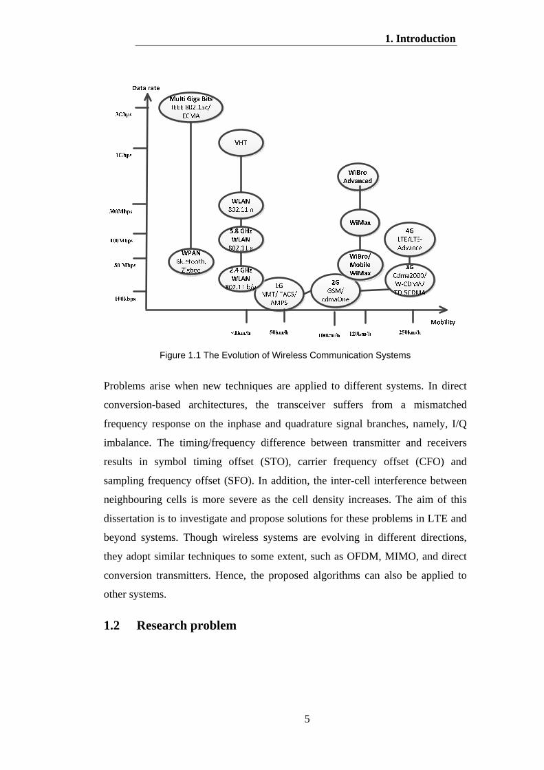
Fig. 1.1 gives an overview of the evolution of different communication standards.
These standards are defined by standardization bodies, such as: IEEE,
Standardization of Information and Communication Technology and Consumer
Electronics (ECMA), European Telecommunications Standards Institute (ETSI),
and the International Telecommunication Union (ITU). It can be seen from this
figure that all wireless communication technologies are evolving towards high
speed and high mobility. And there is also an evident trend that different wireless
technologies are merging together.
1. Introduction
5
Figure 1.1 The Evolution of Wireless Communication Systems
Problems arise when new techniques are applied to different systems. In direct
conversion-based architectures, the transceiver suffers from a mismatched
frequency response on the inphase and quadrature signal branches, namely, I/Q
imbalance. The timing/frequency difference between transmitter and receivers
results in symbol timing offset (STO), carrier frequency offset (CFO) and
sampling frequency offset (SFO). In addition, the inter-cell interference between
neighbouring cells is more severe as the cell density increases. The aim of this
dissertation is to investigate and propose solutions for these problems in LTE and
beyond systems. Though wireless systems are evolving in different directions,
they adopt similar techniques to some extent, such as OFDM, MIMO, and direct
conversion transmitters. Hence, the proposed algorithms can also be applied to
other systems.
1.2 Research problem

1. Introduction
6
Figure 1.2 Typical LTE Network.
To achieve high capacity, a high data rate, and good quality of service in LTE, the
3GPP has proposed a variety of techniques including MIMO, OFDMA, AMC,
and heterogeneous networks. Fig. 1.2 presents a typical heterogeneous LTE
network in which a macro cell and femto/pico cell coexist [10], [11]. In this
network, multimedia/voice services are delivered by the radio link between macro
cell and user equipment (UE). To complement the conventional macro cell, low
power pico/femto cells also provide an LTE connection with a much smaller
coverage, which increases system capacity and extends system coverage [12].
However, there exist many problems when implementing such a system in the real
world. This section will describe research problems in two aspects: I/Q imbalance
and receiver algorithm.
1.2.1 I/Q imbalance
I/Q imbalance is mainly caused by hardware impairments of transceivers, which is
a common problem in wireless transceivers. One goal of this thesis is to
investigate into the transmitter I/Q problem.
Direct conversion transmitter is adopted due to its low cost, low complexity and
flexibility [13], [14], [15], [16], [17]. The direct conversion transmitter (DCT)
utilizes the non-Hermitian symmetry property of the complex signal in the
1. Introduction
7
frequency domain, and modulates this complex signal by suppressing the image
frequency components around the carrier frequency. Ideally, the real and
imaginary part of the baseband complex signal is modulated by a pair of
quadrature mixers on the inphase and quadrature branch respectively.
Theoretically, the image frequency components around the carrier frequency can
be completely eliminated by adding the modulation results of the two branches.
However, the nonideal hardware devices result in a mismatch on the two branches
[18], [19]:
1). DAC and low pass filters on the baseband modules bring mismatched
amplitude and phase delay due to non-linearity.
2). The two local oscillators (LO) of the mixer do not have the same amplitude
and 90° phase difference.
3). The RF amplifier and radio signal path on the two branches exhibit
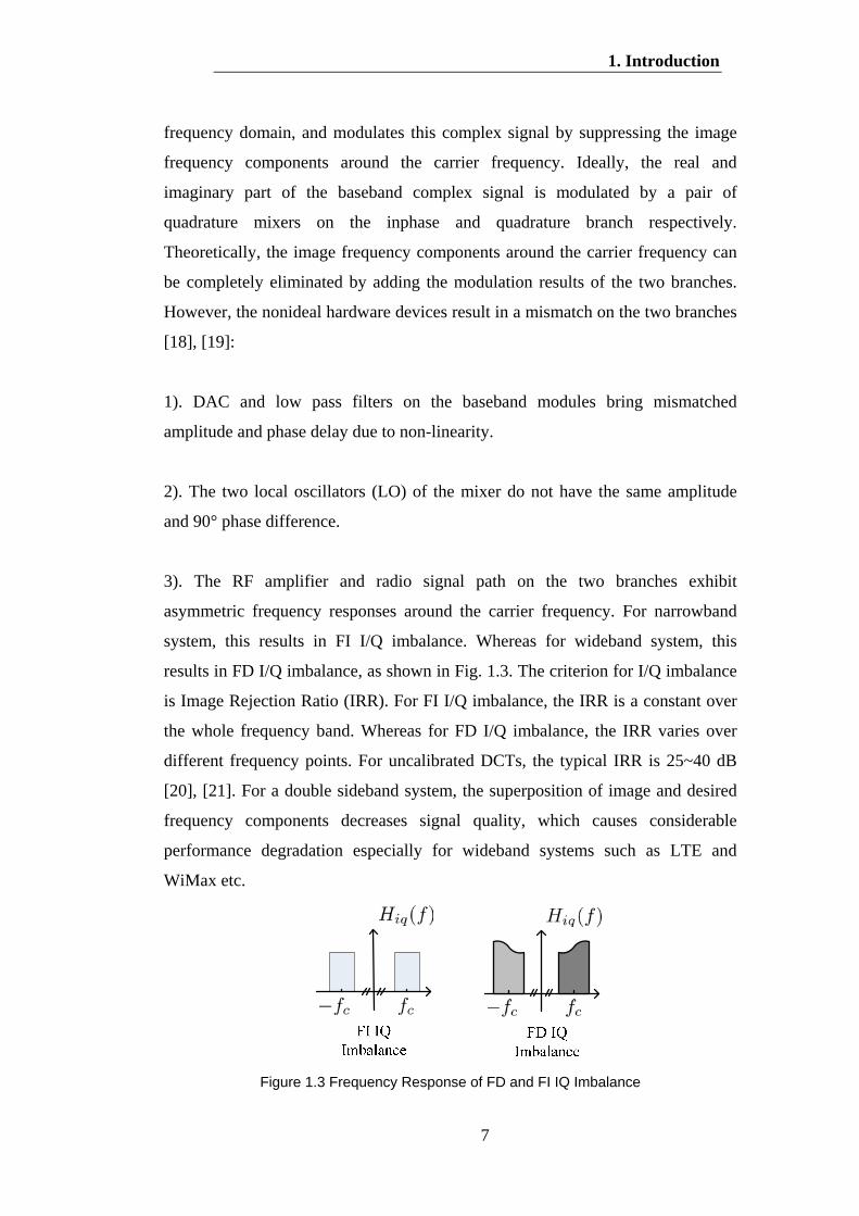
asymmetric frequency responses around the carrier frequency. For narrowband
system, this results in FI I/Q imbalance. Whereas for wideband system, this
results in FD I/Q imbalance, as shown in Fig. 1.3. The criterion for I/Q imbalance
is Image Rejection Ratio (IRR). For FI I/Q imbalance, the IRR is a constant over
the whole frequency band. Whereas for FD I/Q imbalance, the IRR varies over
different frequency points. For uncalibrated DCTs, the typical IRR is 25~40 dB
[20], [21]. For a double sideband system, the superposition of image and desired
frequency components decreases signal quality, which causes considerable
performance degradation especially for wideband systems such as LTE and
WiMax etc.
Figure 1.3 Frequency Response of FD and FI IQ Imbalance

1. Introduction
8
There has been much research into I/Q imbalance calibration. The works in [13],
[22], [23] and [24] estimate the I/Q imbalance of the narrow band signal, which
relies on the assumption that I/Q imbalance is frequency-independent (FI) within
the signal band, whereas the studies in [25], [18], [26] and [27] address FD I/Q
imbalance which is common in wideband DCTs. In terms of realization
architecture, the transmitters in [22], [13] and [28] utilize a diode or power
detector circuit to estimate the I/Q imbalance. This architecture usually requires
predefined test tones, which indicates the estimation is off-line. Besides, low-IF
architecture is most popular in I/Q calibration [25], [26] and [27]. In this
architecture, the external down converter and ADC forms a low-IF receiver. Due
to this extra receiver, on-line estimation can be realized.
For the aforementioned diode based approaches, test signals are generated by the
transmitter, and the output of the diode or power-detector is sampled by the ADC.
These kinds of methods make use of the square law of the diode. Because it
assumes the I/Q imbalance is FI, the target estimation parameters are only the LO
mismatch and DC offset.
In [29], the author transmits a two-tone signal and the output of the diode carries
the information pertaining to the LO mismatch. The two-tone signal modulates
with itself in the diode. The output signal can be represented by an information
array of LO and DC offset parameters. Then, this information matrix can be
estimated by using Least Square (LS) methods. This method brings reasonable
image suppression improvement within a 5 MHz bandwidth. However, it requires
considerable computation resources when the sampling data increases as the LS
methods employ a matrix inversion operation. Based on the same feedback path,
the author proposes the low computation complexity method in [22], The output
of the diode is a monotonic function . Hence, the author proposes to calibrate such
DC offsets by iteratively tuning the input to DC level. Similarly, the gain has a
straightforward influence on the diode output. Hence, the gain imbalance can be
calibrated in the same way. For phase imbalance, the output of the diode is an
ellipse function of phase error, which indicates the phase error is calculated by

1. Introduction
9
solving different sampled ellipse functions. In general, the diode based method
provides a low cost solution for LO I/Q imbalance. However, it is a constraint to
narrow the band signal.
For low-IF based methods, an external receiver or internal feedback path which
consists of a downconverter, ADC, and digital signal processor (DSP), is
introduced to measure the I/Q imbalance parameters. The RF signal is
downconverted to low intermediate frequency (IF) and then digitized by the ADC.
The digital signal is then I/Q demodulated by digital I/Q demodulator, which
enables it to measure the wideband FD I/Q imbalance.
In [22], the I/Q imbalance is calibrated pair-by-pair which assumes there are no
image components during the calibration stage. In [25], only the mismatch of
DAC and signal path is considered, whereas the mismatch of LO is assumed to be
ideal. These methods make use of wideband receiver and design special test
signals. Apart from this, [18] and [26], the cross-processing between I and Q
signal and LS methods are used to estimate the imbalance parameters. These
approaches are applicable to the majority signal which indicates on-line
calibration can be realized. [18] studies the second-order statistics of the complex
random signal and takes into account the overall frequency response of the
internal feedback path. A widely linear (WL) LS method is proposed in which the
FD I/Q parameters are calculated by applying the pseudo-inverse of the
transmitted signal matrix. This method provides a flat 75 dB image rejection ratio
within a 10 MHz bandwidth. However, an ill conditioning matrix can happen
when the signal is narrowband. In general, low-IF based methods provide a good
on-line solution to calibrate an FD I/Q imbalance which is crucial for wideband
systems such as LTE, DVB and WiMax . However, the cost and implementation
complexity is relatively high because an extra downconverter and IF frequency
source are introduced.
In summary, there still exist some problems for both diode and low-IF based I/Q
imbalance compensation schemes:

1. Introduction
10
1). For diode based schemes, it can effectively measure the I/Q imbalance at
low cost. Because the power detection in most DCTs is a low pass filter, the
output of diode will be constraint to narrowband. Hence, the conventional diode
based I/Q imbalance estimation schemes loss the wideband I/Q imbalance
information.
2). For low-IF based schemes, the low-IF receiver can effectively estimate
wideband I/Q imbalance. However, the cost will be high, because extra mixer and
LO is introduced.
This paper aims to propose a low wideband (FD) I/Q imbalance compensation
scheme that makes use of cost diode, which will be presented later.
1.2.2 Receiver algorithm
The received signal on the receiver side may experience severe deterioration due
to a variety of influences:
1). As shown in Fig. 1.2, the propagation condition of the RF signal is complex.
Due to multi path effects and reflections, the replicates of the transmitted signal,
with different amplitude and phase delay, will arrive at the receiver side
simultaneously. As a result, the channel exhibits a frequency selective fading [21],
[30] and [31]. For UEs that are moving, the channel condition may change rapidly
due to the Doppler effect. As a result, the channel will be time-varying as well
[32]. For OFDM systems, this induces Inter-Symbol Interference (ISI) and Inter-
Carrier Interference (ICI) [33].
2). Nonideal frequency sources generate different reference frequencies at the
transmitter and receiver side. In addition, the reference frequency will drift with
varying temperature and unstable power supply. Hence, the unsynchronized
reference frequency causes CFO and SFO, which destroy the orthogonality among
all sub-carriers of the OFDM signal. This results in ICI [34]. For LTE UEs, the
typical CFO is 25 KHz, which is ±1.67 subcarrier spacing with an SFO of about
10 ppm [35]. Besides this, there exists a timing offset. As the OFDM signal is

1. Introduction
11
transmitted symbol by symbol, the receivers usually have no prior information
about when the symbols start. This induces a timing offset which significantly
influences the following signal demodulation process [21].
Much literature examines these problems. The majority of research treats the
influence of CFO and a fading channel jointly, see [36], [37] and [38]. In [37], the
channel is modelled by a basis expansion model (BEM) to reduce the amount of
estimation parameters. The CFO ad BEM coefficients are jointly estimated by a
pilot-based maximum a posteriori (MAP) technique. An iterative soft decoder is
adopted to improve performance. This algorithm achieves close to the ideal
performance. Similarly, [36] proposes a recursive least-square (RLS) method to
estimate CFO, SFO and channel impulse response (CIR) jointly. A simple
maximum-likelihood (ML) estimator provides a coarse estimation of CFO and
SFO based on the training signal. The coarse estimation results are then fed into a
fine estimator, where the CIR, CFO and SFO is estimated by optimizing the LS
cost function on the corresponding pilot tones. Though the BEM model and ML
method help to reduce estimation parameters, the MAP algorithm and cost
function optimization consume considerable computation resources to achieve
good performance. This class of joint estimation approaches mainly makes use of
a certain cost or probability function, which requires iterative optimization and is
computationally heavy. Instead, [39] thoroughly investigates the impact of the
above individual impairments: imperfect channel estimation, STO, CFO and SFO.
An optimization criterion based on SNR loss is developed. And the minimum
requirements on each module are systematically derived. Based on the results in
[39], [40] designs a complete receiver to cope with the above impairments. The
impact of synchronization algorithms and complexity is qualitatively analysed. As
the LTE system is evolving in the direction of high data rate, high mobility, an
optimum receiver is required. These two pieces of research provide a good
reference point for the receiver algorithm design in this dissertation.
The estimation error contributes to the ICI and ISI [39]. A robust equalizer is
required to mitigate this impact. Equalizers can be categorized into zero-forcing

1. Introduction
12
equalizer (ZFE), minimum mean square error linear (MMSE-LE) and decision-
feedback equalizers (MMSE-DFE) [41]. ZFE provides simple architecture but
often limited effectiveness. MMSE-LE and MMSE-DFE is more widely used
because of higher performance. MMSE-LE performs better than ZFE because of
noise enhancement in which coloured noise will be whitened. MMSE-DFE
exhibits superior BER performance compared to linear equalizers such as ZFE
and MMSE-LE [42]. [41] presents a serial MMSE-DFE which is suitable for
serial QAM modulation. It makes use of the statistics of serial channel
information and yields good performance. However, this is not suitable for block
transmission such as OFDM in LTE systems. [43], [44] and [42] investigates the
MMSE-DFE in block transmission. The MMSE-DFE is derived using the
orthogonal principle and MMSE criteria based on the assumption that the
feedback filter is upper triangular. However, these approaches are computationally
heavy, for it calculates the feedback and feedforward filters through Cholesky
factorization.
SNR provides channel and signal condition criteria to channel equalizers. The
most popular SNR estimation algorithm is the moving average method [45].
However, the method is inaccurate in time variant channel in LTE system. The
data-aided methods in [46] and [47] realize accurate SNR estimation, which
requires a specially designed data sequence. [47] proposes a subspace-based
algorithm which is robust in time variant channel. However, it is not compatible
with LTE pilot structures: the accuracy decreases when the signal is narrowband
or assigned to distributed resource blocks. Hence, a robust SNR estimation
algorithm is required in this context. To sum up, many problems arise and cause
significant performance degradation when an LTE OFDM receiver is applied to a
high mobility and complexity environment.
Apart from the above impairments caused by the channel and transceiver, there
exists interference from other cells. As shown in Fig. 1.2, the UEs in
heterogeneous LTE can acquire service via pico/femto cells due to reasons of data
traffic offloading, lower system power or range extension [48], [49]. However,

1. Introduction
13
when the UE is served by one cell, e.g. pico/femto, it still receives a signal from
macro cells when it is located in the cover of the macro cell. This inter-cell
interference severely degrades signal quality. Though an enhanced inter-cell
interference cancellation (eICIC) scheme is proposed after LTE Release 10 [50],
the UE suffers from residual cell specific reference signal (CRS) interference [51].
Solutions such as direct CRS cancellation, data muting and LLR puncturing are
studied in [52] and [53], which reveals direct CRS cancellation, achieving
superior interference cancellation (IC) performance. [54] and [55] proposes two
methods that make use of a classical channel estimation algorithm. However,
these methods are suitable for a non-synchronized interference signal.
In summary, the problems this thesis will address are:
1). Though there exists some receiver algorithms, the receiver in 5G will still
face CFO, SFO, STO and channel problems. In terms of complexity and
verification, these algorithms are still complex to be implemented in DSP or
FPGA.
2). For fast fading channel, it still requires an accurate SNR estimation
algorithm to support further equalization in receiver.
3). For future heterogeneous network, the receiver may face severe inter-cell
interference. Though ABS scheme is proposed to alleviate this, the remaining
CRS still cause interference.
These problems are crucial for LTE system performance. This dissertation deals
with the above problems with low cost and high performance solutions. The other
effects of transceiver nonidealities, such as non-linearity of amplifier, receiver I/Q
imbalance, are out of the scope of this dissertation.
1.3 Objectives and solution approach
The overall objective of this dissertation is to provide solutions that optimize LTE
transceiver performance. More specifically, the dissertation overcomes the
previously mentioned problems with low cost and high performance methods:

1. Introduction
14
1. Develop a low cost automatic I/Q imbalance compensation scheme for
DCTs.
In order to reduce the cost of FD I/Q imbalance compensation, diode-based
compensation scheme will be adopted. This paper will firstly investigate into
the conventional diode-based I/Q imbalance compensation scheme. Then the
feasibility of diode-based scheme for FD I/Q imbalance will be discussed. In
order to estimation and compensate FD related I/Q imbalance factors, this
thesis will investigate DCT hardware impairments and analyze factors that
cause I/Q imbalance. This should cover wideband scenarios in which I/Q
imbalance is FD. Based on this, FD I/Q imbalance model will be derived for
development of I/Q imbalance estimation and compensation algorithm.
A low cost estimation and compensation algorithm that combines the
advantage of diode and low-IF schemes will be proposed based on the derived
model. The estimation algorithm aims to estimate overall FD I/Q imbalance for
any modulation scheme (QPSK, QAM, etc.). It can estimate the amplitude and
phase imbalance caused by pure LO. The compensator should be based on a
baseband digital signal processing algorithm. It should be able to compensate
the FD I/Q imbalance. The whole compensation scheme should be low cost,
possess low computational complexity, and be automatic with IRR
improvement larger than 10 dB. Because the output of diode contains abundant
harmonics, which degrades the estimation performance, this scheme designed
single tone for estimation, whereas the conventional low-IF schemes adopt
multi-tone estimation. In addition, this scheme does not take the non-linearity
of amplified into account. Furthermore, the work will be on joint estimation of
I/Q imbalance and non-linearity by designing special training sequence.
2. Develop LTE downlink receiver algorithm with inter-cell interference
cancellation capability.

1. Introduction
15
The downlink receiver algorithm should take into account the detrimental
effects of CFO, SFO, frequency and time selective channel (doubly selective
channel), and timing offset. The downlink receiver algorithm should be able to
be applied in typical mobile scenarios, e.g. 25 KHz CFO, 10 ppm SFO, fading
channel with 50 Hz Doppler frequency. Apart from this, the receiver should be
able to cope with CRS interference from neighbouring cells.
Based on existing algorithms, the hybrid receiver will be developed. This
receiver makes use of some conventional frequency/timing synchronization
and channel estimation methods, which is able to estimate and compensate
timing offset, CFO, SFO, and doubly selective channel with low computational
complexity. The computation complexity of these methods are low, which is
easy for further implementation and verification. In addition, an MMSE-DFE is
derived to alleviate the residual impairments. Unlike the conventional MMSE-
DFE that is derived by using matrix factorization, the factors of proposed
MMSE-DFE are derived by using Lagrange Multiplier, which reduces the
computation burden. Simulation results show that the receiver algorithm give
satisfactory performance with low implementation cost. The proposed DFE
gives similar performance as the convetional DFE does. However, the
simulation also shows that the proposed DFE brings limited performance
improvement at the cost of high computation burden.
In order to perform accurate SNR estimation, this thesis proposed a sub-space
based SNR estimation algorithm. By doing eigen-decomposition to the
covariance matrix of received signal and estimating channel length, the power
of signal and noise could be obtained from eigenvalues. In addition, this thesis
proposed an inter-cell interference cancellation algorithm. The algorithm firstly
makes use of statistics of received signal. The channel response could be
estimated then. Afterwards, the interfering signal could be reconstructed and
subtracted from the received signal. Simulation results show that the proposed
algorithm gives much less estimation error compared with classical sub-space
methods over the interested algorithm under different time-varying channels.

1. Introduction
16
The simulation results show that the proposed algorithm is robust for different
pilot patterns. However, it shows that this algorithm gives considerable
estimation error when larger numbers of pilots is used and SNR is high. It is
recommended that less numbers of pilots to be used for SNR estimation, which
is more robust and consumes less computation resources.
In addition, this thesis also investigated into the problem of CRS interference
in the future heterogeneous networks. The signal structure and interfering
channel conditions will firstly be analysed. Then an algorithm that makes of
channel statistics is proposed. As the channel in this scenario is slow fading,
the interfering channel could be accurately estimated by moving average
method. Then the interfering signal could be locally reconstructed and
subtracted from the received signal. Simulation results show that this algorithm
significantly improves the block error rate (BLER) performance under different
channels and MCS. It also shows that this method is robust to timing and
frequency error at the cell edge. This method estimates timing and frequency
error by using synchronization symbols, where the number of synchronization
symbols is limited. Hence there could be an issue that inaccurate timing and
frequency estimation is conducted when SNR is low. Future work will be on
accurate timing and frequency synchronization by making use of pilot symbols.
Although there exist I/Q imbalance compensation schemes and wireless receiver
algorithms in many literatures [13, 18, 19, 21, 32, 37, 39], this dissertation will
present innovative, low cost and high performance solutions for LTE transceivers,
detailed in the following chapters.
1.4 Outline of the thesis
The structure of this dissertation and its major contributions are:
Chapter 2 presents a general overview of a system model for LTE downlink
physical layer. The model takes into account the important aspects of LTE
downlink communication link. A brief overview of typical LTE transceiver

1. Introduction
17
architecture, along with some of the most common hardware impairments, is
presented including the principle of DCT transmission, I/Q imbalance, and
frequency offsets. Then, the frequency-time selective channel model in different
propagation scenarios is introduced. The LTE physical layer standards and the
existing eICIC scheme are presented. The research in the subsequent chapters will
be based on these models.
Chapter 3 focuses on the DCT I/Q imbalance compensation scheme. The FD I/Q
imbalance model will be derived to develop a novel estimation algorithm. The
characteristics of transmitter devices such as mixer, and power detector, will be
analyzed in detail. The principles of conventional estimation methods will be
presented and analysed. Based on this, a self-IQ-demodulation based estimation
method is developed which only requires a transmitter’s internal power detector
and ADC. Accordingly, the corresponding test tone and hardware requirements
will be studied. It will be shown how the LO imbalance parameters and other
nonideal devices can be separately estimated. The FD baseband compensator will
also be introduced. Finally, the overall performance of the proposed scheme will
be assessed using a computer and laboratory instruments.
Chapter 4 investigates the optimum OFDM receiver for the LTE downlink
receiver. The impact of CFO, SFO and doubly selective channel will be presented.
Then, a hybrid estimation scheme is proposed. Within this scheme, joint
estimation algorithms will be adopted to deal with the impact of CFO, SFO, and
doubly-selective channel. A low cost minimum mean square error (MMSE)
decision feedback equalizer (DFE) is developed to minimize the error. In addition,
an FPGA-based co-simulation platform is built to speed up the algorithm
verification process. The overall performance of the whole compensation scheme
is verified by computer simulation and the co-simulation platform.
Chapter 5 proposes a subspace-based noise estimation algorithm for time-varying
channels. The requirements for SNR estimation in LTE systems are analyzed and
it will be shown that the conventional moving average based SNR estimation

1. Introduction
18
method gives biased estimation in time-variant channels. The eigenvalue
decomposition for the signal correlation matrix shows that the received signal
space can be divided into signal space and noise space. Signal and noise power is
projected into these two spaces. The MDL method and modified MDL method is
applied to estimate the noise power. Simulation results verify the robustness of
this method.
Chapter 6 presents another contribution, which aims to alleviate the CRS
interference. The CRS interference scenario and the major factors of CRS
interference on the receiver side will be represented. The dominant STO and CFO
are compensated by exploiting the synchronization channel. Then, the statistics of
the interfering channel of the neighbouring cell will be investigated, according to
the information of the LTE control channel. Based on this, an interference
reconstruction and a cancellation algorithm are proposed. Computer simulation
verifies the effectiveness of this proposed algorithm in different scenarios.
Chapter 7 concludes the contributions of this dissertation and puts forward
potential further research directions.
1.5 Main contributions The main contributions of this thesis are to:
1. Designed a new FD I/Q imbalance calibration scheme for DCTs. Achieved
satisfactory performance for both, and narrowband signals. Reduced the
overall feedback cost. Verified the feasibility of using a self-IQ-
demodulation method to calibrate I/Q imbalance and other non-linear
distortions.
2. Designed a computationally low complexity OFDM receiver which adopts
the simplified MMSE-DFE. Designed a co-simulation platform and speed
up the algorithm verification process.

1. Introduction
19
3. Proposed a robust SNR estimator for flexible pilot allocation scenarios for
a time variant channel.
4. Proposed a robust CRS interference cancellation algorithm that is robust
for timing and synchronization errors.
1.6 Papers published and submitted
The following papers and reports have been published and submitted to journals,
conferences and companies, that report the results of this thesis:
1. Wei Li, Yue Zhang, Li-Ke Huang, Jian Xiong, C. Maple, “Diode-based IQ
imbalance estimation in direct conversion transmitters”, Electronics Letters,
Vol. 50, Issue 5, pp. 409-411 Feb, 2014
2. Wei Li, Yue Zhang, Li-Ke Huang, C. Maple, J. Cosmos, “Implementation
and Co-Simulation of Hybrid Pilot-Aided Channel Estimation With
Decision Feedback Equalizer for OFDM Systems”, IEEE transaction on
Broadcasting, Vol 58, Issue 4, pp. 590-602, Dec. 2012
3. Wei Li, Yue Zhang, Li-ke Huang, Jin Wang, John Cosmas, Carsten Maple,
Jian Xiong, “Self-IQ-Demodulation Based Compensation Scheme of FD IQ
Imbalance for Wideband Direct-Conversion Transmitters”. Submitted to
IEEE Transactions on Broadcasting
4. Wei Li, Yue Zhang, Li-ke Huang, John Cosmas, Qiang Ni,” 2015 IEEE
International Symposium on Broadband Multimedia Systems and
Broadcasting (BMSB 2015), Jun. 2015, Ghent
5. Wei Li, Yue Zhang, Li-ke Huang, John Cosmas, Carsten Maple, Jian Xiong,
“Self-IQ-Demodulation Based Compensation Scheme of FD IQ Imbalance
for Wideband Direct-Conversion Transmitters '', 2014 IEEE International
Symposium on Broadband Multimedia Systems and Broadcasting (BMSB
2014), Jun. 2014, Beijing
6. Wei Li, Yue Zhang, Yuan Zhang, Li-ke Huang, J. Cosmos, C. Maple,
“Subspace-Based SNR Estimator for OFDM System under Different

1. Introduction
20
Channel Conditions”, 2013 IEEE International Symposium on Broadband
Multimedia Systems and Broadcasting (BMSB 2013), Jun. 2013, London
7. Wei Li “Aeroflex PXI 3050 Signal Generate IQ Imbalance Calibration Test
Report”, Aeroflex, Stevenage, Oct. 2012

21
2. Physical Layer Model of LTE and Beyond Systems
2.1 Introduction
As an IP based network, LTE Radio Access Network (RAN) provides access to
core networks with the functionalities of Radio Resource Control (RRC), Packet
data Convergence Protocol (PDCP), Radio Link Control (RLC), Media Access
Control (MAC) and Physical Layer (PHY). Fig. 2.1 demonstrates a brief LTE
network topology. The upper layers process the packet data from/towards the core
network and the PHY then conveys the information from the upper layers through
physical channels [10, 11, 29, 56]. This dissertation will focus on the physical
layer, which is responsible for the bottommost data exchange process in the
network. The other functionalities of PHY, such as link adaption and power
control, are out of this dissertation’s scope.
The 3GPP LTE standards specify all of the PHY techniques. LTE standards first
began to be examined in 2004. In 2008, 3GPP Release 8 was completed, this
serving as the first specification of LTE. In this Release, techniques of OFDMA,
MIMO, automatic modulation and coding (AMS) were specified. The complex
data is conveyed by groups of resource blocks (RB) in an OFDMA time-
frequency grid. Different physical channels are specified to carry control,
synchronization, and user data [10]. The maximum bandwidth is 20 MHz. Up to
MIMO in downlink is supported in this release. In the coming Release 12,
maximum bandwidth is enlarged to 40 Mhz with the help of a carrier aggregation
technique and massive MIMO is adopted. Turbo code is employed to mitigate
channel effects [41]. In Release 9, the concept of heterogeneous network was
introduced in improve system coverage, capacity and power efficiency. This also
included a coordinated multipoint technique, to enable the dynamic coordination
of transmission and reception between different cells. The enhanced interference
coordination (eICIC), which is based on inter-cell interference coordination (ICIC)

2. Physical Layer Model of LTE and Beyond Systems
22
in Release 9, was introduced to cope with inter-cell interference. Further eICIC
(FeICIC) is proposed for Release 12, to cancel the residual interference due to the
densification of cells and interconnections [5].
Figure 2.1 LTE Network Topology
As Fig. 2.1 shows, the LTE PHY can be divided into digital and analog domain.
On the transmitter side, in order to achieve a high data rate and combat
impairments, the information from the upper layer is processed by several
functional modules, such as channel coding, layer mapper, OFDM [29, 56]. Then
the data is presented to the analog domain in the form of a complex signal which
allows for higher frequency efficiency and a lower data rate than the real signal
[57],[58]. The digital complex signal will first be converted to a baseband analog
complex signal. The baseband analog signal is up-converted to the desired RF
band and then amplified. Finally, the transmitter antenna sends the RF signal to
the receiver side via a multipath channel.
The receiver antenna then picks up the corrupted RF signal. Inside the receiver,
the received weak RF signal will be amplified and down-converted to baseband.
During this process, the receiver adopts direct conversion or superheterodyne
technology to recover the baseband complex signal from the real RF signal. The
analog signal is then digitized and transferred to the digital domain again. In the
digital domain, the receiver algorithm deals with the effects of impairments from
non-linearity, the fading channel, and additive white noise etc. Afterwards, the
decoded signal can be recovered by reverse operations to that of the transmitter.

2. Physical Layer Model of LTE and Beyond Systems
23
This decoded data is then finally sent to the upper layer for further processing [16],
[59] and [60].
The remaining part of this chapter will firstly give a brief description of the direct
conversion transceiver model and its impairments. Then, the multipath wireless
channel model and the OFDM signal model will be introduced. Later, the LTE
physical layer standard, including signal structure, key techniques and eICIC
scheme, will briefly be presented for further study.
2.2 Transceiver impairments
The PHY transmitter and receiver can be implemented based on superheterodyne
or direct conversion architecture [59-61]. Superheterodyne architecture realizes
complex signal modulation/demodulation by using an RF stage and an
Intermediate Frequency (IF) stage [57, 60, 62]. In contrast, direct conversion
architecture realizes complex signal modulation/demodulation by using only one
frequency on one stage. Superheterodyne architecture is less popular than direct
conversion architecture due to complexity and cost reasons [57, 60]. The
discussion of this dissertation will be based on direct conversion architecture.
2. Physical Layer Model of LTE and Beyond Systems
24
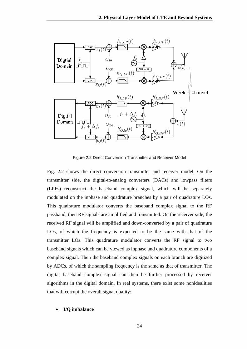
Figure 2.2 Direct Conversion Transmitter and Receiver Model
Fig. 2.2 shows the direct conversion transmitter and receiver model. On the
transmitter side, the digital-to-analog converters (DACs) and lowpass filters
(LPFs) reconstruct the baseband complex signal, which will be separately
modulated on the inphase and quadrature branches by a pair of quadrature LOs.
This quadrature modulator converts the baseband complex signal to the RF
passband, then RF signals are amplified and transmitted. On the receiver side, the
received RF signal will be amplified and down-converted by a pair of quadrature
LOs, of which the frequency is expected to be the same with that of the
transmitter LOs. This quadrature modulator converts the RF signal to two
baseband signals which can be viewed as inphase and quadrature components of a
complex signal. Then the baseband complex signals on each branch are digitized
by ADCs, of which the sampling frequency is the same as that of transmitter. The
digital baseband complex signal can then be further processed by receiver
algorithms in the digital domain. In real systems, there exist some nonidealities
that will corrupt the overall signal quality:
I/Q imbalance

2. Physical Layer Model of LTE and Beyond Systems
25
The most notorious problem of direct conversion architecture is I/Q imbalance
[16-19]. This is caused by the mismatched LPF, mixer and amplifiers on inphase
and quadrature branches, as shown in Fig. 2.2. A lot of literature investigates FI
I/Q imbalance [13-15]. However, the mismatch will exhibit an FD property for the
wideband signal, which means these models fail to describe the wideband
scenario. In this dissertation, the wideband frequency response of LPFs, mixers
and amplifiers will be modelled, as shown in Fig. 2.2. Furthermore, a detailed FD
I/Q imbalance model is presented in Section 3.2.
Frequency offset
Apart from the I/Q imbalance problem, frequency and timing error also exerts a
significant impact regarding signal quality. As shown in Fig. 2.2, the quadrature
modulation and demodulation operates with different frequency sources. In
addition, the sampling clocks of ADC and DAC on the transmitter and receiver
sides also operate in accordance with different clock sources. This causes a
frequency offset between transmitter and receiver. For LTE systems, the
demodulation of OFDM signal in the presence of frequency and timing error
destroys the orthogonality of subcarriers. The frequency error is briefly modelled
in Fig. 2.2. Furthermore, Section 4.2 depicts in detail the impact of the frequency
offset.
This dissertation will investigate the effect impairments of transmitter I/Q
imbalance and frequency offset. The other impairments, including receiver I/Q
imbalance and non-linearity distortion, will be modelled as Additive White
Gaussian Noise (AWGN) noise. Furthermore, the baseband equivalent models for
frequency response of transmitter analog devices and frequency offset will be
considered, which makes it straightforward to simulate the whole system. Based
on this baseband equivalent model, a lost baseband compensation technique can
be realized.
2.3 Wireless channel model

2. Physical Layer Model of LTE and Beyond Systems
26
2.3.1 Wireless channel environment
The radio signals are also degrade by the wireless channel. As depicted in Fig. 2.3,
the transmitted radio wave, which will be reflected, attenuated by various
obstacles, travels along a different path before arriving at the receiver antenna. As
a result, the receiver antenna picks the radio signals which consist of different
duplicates of the original signal with different time delays and amplitudes. This
combination of different delayed original signals leads to constructive or
destructive results, known as the 'multipath effect'. Aside from the multipath
effect, the relative dynamic movement of transmitters, obstacles and receivers
causes a time varying effect, which is referred to as 'fading'.
Figure 2.3 Propagation of Radio Signal in Wireless Channel
The channel impulse response (CIR) at time and propagation delay can
be modelled as [63, 64]:
(2.1)
where is the attenuation factor for the signal receiver on the path; is
the delay of path and is the number of path at . Assuming there are a
2. Physical Layer Model of LTE and Beyond Systems
27
great many paths, the channel impulse response can be modelled as a
complex valued Gaussian process according to the central limit theorem. For a
channel that has no fixed reflectors or scatters, the Gaussian process is zero-mean
and has a Rayleigh probability density function (PDF):
(2.2)
where is the envelope of in Eq. (2.1), and is a constant. Another PDF
can be used to model the envelope of the channel with respect to delay and
based on the channel scattering and reflection condition, such as Ricean and
Nakagami-m distribution. The channel model in Eq. (2.1) will be used for
simulation
2.4 OFDM signal model
LTE downlink transmission adopts OFDM modulation. As a special case of
Frequency Division Multiplexing (FDM), OFDM modulates bit streams on
several subcarriers in parallel. In FDM systems, the data bits are modulated by
different subcarriers and these subcarriers are separated by a guard band in the
frequency domain to prevent the overlap between different subcarriers, as shown
in Fig. 2.4. The extra guard band reduces the spectral efficiency. By contrast, an
OFDM system utilizes the overlapped subcarriers which are orthogonal to each
other. Because of orthogonality, the subcarriers of interest locate on the nulls of
the other subcarriers without introducing any interference to the subcarriers of
interest, as shown in Fig. 2.5. The OFDM system avoids using the guard band in
this way and achieves higher spectral efficiency. Another benefit is that the bit
rate could be reduced as data streams can be transmitted on different subcarriers in
parallel. As a result, the symbol duration is increased. And the system is more
robust to the frequency-selective channel if it has longer symbol duration than the
maximum delay spread .

2. Physical Layer Model of LTE and Beyond Systems
28
The FMD signal can be expressed in the linear form:
(2.3)
where is the coefficient of subcarrier; is the number of subcarriers and
is expression of subcarrier in time domain:
(2.4)
where is the time window for the symbol of interest. For the sake of
simplicity, the rectangular window with length of is used:
(2.5)
Figure 2.4 Subcarriers in FDM Systems

2. Physical Layer Model of LTE and Beyond Systems
29
Figure 2.5 Subcarriers in OFDM Systems
The window length can also be viewed as the symbol period. In OFDM, the
subcarriers are orthogonal to each other, hence the subcarriers satisfy the
following relationship:
(2.6)
Substitute Eq. (2.4) for the in Eq. (2.6), there is:
(2.7)
In solving this equation, we have . This shows that, in order to
meet the requirement for orthogonality, the subcarrier spacing should be a
multiple of . This can be verified with the Fourier transform of Eq. (2.3):

2. Physical Layer Model of LTE and Beyond Systems
30
(2.8)
According to Eq. (2.8), the OFDM signal can be viewed as the summation of
several sinc functions with a frequency shift of as shown in Fig. 2.5. As the
nulls of sinc function locate on , the overlapping of a different subcarrier
does not bring interference to the frequency points . The orthogonality
between different subcarriers is achieved in this way. However, this is vulnerable
to frequency offset. If the orthogonality is broken by the carrier frequency offset
or Doppler effect, the side lopes for the other subcarrier will accumulate at the
interested frequency point, which causes inter-carrier interference (ICI).
Due to the stringent requirement for subcarrier orthogonality, it is difficult to
generate the OFDM signal using analog devices. Instead, the digital signal process
(DSP) technique makes it possible to generate an OFDM signal by Inverse Fast
Fourier Transform (IFFT). If the subcarrier of OFDM signal with frequency
and in Eq. (2.3) is processed in the digital domain with the sampling
frequency , then Eq. (2.3) in the digital domain can be rewritten as:
(2.9)
where . It shows that the time domain OFDM can be easily obtained by
applying IFFT to the frequency domain data. Thus, the generation of an OFDM
symbol can be summarized as:

2. Physical Layer Model of LTE and Beyond Systems
31
In order to achieve orthogonality, the subcarrier spacing is set to multiple of
symbol rate . Then, the data in the frequency domain is assigned to every
subcarrier’s frequency for modulation. Afterwards, the time domain OFDM signal
is generated by applying IFFT to the corresponding frequency domain data. With
the development of DSP, the implementation of IFFT operation becomes cheap
and fast – Dedicated IFFT core is embedded in the chip and it only takes several
clock periods to complete the IFFT operation.
Thesymbol length will be extended by maximum delay spread when passing
through the frequency selective channel, which causes ISI between adjacent
symbols. Inserting a guard interval (GI) between the symbols can prevent ISI.
Furthermore, OFDM avoids this problem by inserting a Cyclic Prefix (CP) in the
GI. As shown in Fig. 2.10, the content of CP is the copy of last OFDM symbols
with length longer than . When transmitting in the frequency selective channel,
the interference from the previous symbols is limited within the CP. At the
receiver side, the CP part will be removed. In this way, the remaining
uncontaminated part can still retain more than one cycle of subcarriers as shown
in Fig. 2.6, which guarantees orthogonality among subcarriers.
After the insertion of CP, the time window expands to where
is the length of CP and the symbol length without CP. Hence the
transmitted OFDM symbol in a successive transmission is expressed as:
Figure 2.6 Cyclic Prefix in OFDM
(l-1)th OFDM Symbol
lth OFDM Symbol
(l+1)th OFDM Symbol
CP
Integer Cycles
2. Physical Layer Model of LTE and Beyond Systems
32
(2.10)
where is the window function specified in Eq. (2.5).
Using the channel model in Section 2.3, the received signal can be represented as:
(2.11)
where is the additive noise. In the frequency domain, this can be expressed as:
. Intuitively, it is easy to recover the transmitted
OFDM signal with . The receiver utilizes the OFDM signal
structure and recovers as follows:
After the received signal is sampled by the receiver ADC, the CP is removed and
FFT is carried out to get the received signal . Then the transmitted signal is
obtained by doing equalization , where is the estimation of
channel frequency response. This method is effective because of the special
design of the OFDM signal structure. Firstly, the influence of the previous symbol
is restricted, which means that the remaining part is immune to the ISI from the
previous symbol. Hence, is only contaminated by the frequency-selective
fading channel and the additive noise. Secondly, the content in CP, is the copy of
the last few pieces of data in the OFDM symbol, which makes it equivalent to
circular convolution, whereas the effect of the channel is a linear convolution
process. In other words, the circular convolution which corresponds to
equals the linear convolution in operation , thus the signal
can be recovered. More specifically, the CP can be regarded as the periodic
extension of the OFDM symbol with a period of . As maximum delay spread
is shorter than the CP length , the linear convolution of CP is repeated at the
last part of the OFDM symbol. As a result, the linear convolution in the channel
contamination process becomes circular convolution and the transmitted signal

2. Physical Layer Model of LTE and Beyond Systems
33
can be recovered. This equalization method provides a very simple way to recover
the transmitted signal compared with the inverse convolution method.
Though OFDM brings these benefits, it is vulnerable to frequency offset. As the
orthogonality is based on accurate superposition of subcarrier, any frequency
offset will result in side lobes of the other subcarriers overlapping the interested
subcarrier, which introduces ICI. This frequency offset could be caused by CFO,
SFO or even Doppler frequency shift. Hence, the frequency offset estimation and
compensation is important and will be discussed in the following chapters.
2.5 LTE PHY standards and eICIC
Throughout this dissertation, the enhancement technique is developed for LTE
systems. However, the proposed algorithms are also suitable for other OFDM
systems which operate in similar environments and platforms. LTE adopts several
new techniques to improve data rate and signal qualities. This dissertation studies
algorithms related to the following techniques:
OFDMA
Orthogonal Frequency-Division Multiple Access (OFDMA) is adopted in LTE
downlink, and Single-Carrier Frequency-Division Multiple Access (SC-FDMA) is
used in uplink because of lower peak-to-average ratio (PAR). This dissertation
will focus on the downlink transmission. For a more in depth study of the uplink
transmission, the reader is referred to [56, 65]. OFDMA is an access scheme that
is based on the OFDM principle to arrange the distribution of radio resources for
multi users. In OFDMA, the radio resources can be allocated flexibly to a specific
user at different time instances. Fig. 2.7 gives a brief illustration of OFMD and
OFDMA principles. The OFDM symbols which carry data for different users are
mapped to radio resources. The radio resources (subcarrier) distributes on the
appropriate frequency and time grids. Unlike the pure OFDM technique, the radio
resources in such an OFDM symbol can be allocated to different users according

2. Physical Layer Model of LTE and Beyond Systems
34
to the channel conditions. This flexible access scheme improves the spectral
efficient as the scheduler allocates the radio resources to the users in an optimized
way. As a special access scheme of OFDM, OFDMA demonstrates the
advantages of robustness against frequency-selective channels.
Figure 2.7 Brief Illustration of OFDM and OFDMA
Multiple-Input and Multiple-output (MIMO) Antenna
LTE adopts the MIMO technique to improve the data rate and spectral efficiency.
The eNodeB supports up to 4 transmit antenna ports and 4 receive antenna ports.
Up to 2 receive antenna ports and 1 transmit antenna port can work
simultaneously in UE. Fig. 2.8 shows three main MIMO techniques that can
improve the signal quality and channel capacity:
1). Beamforming. This technique concentrates the radio beam to a specific
spatial direction which improves power efficiency and reduces interference. This
is achieved by the beam destructive and constructive interference of the precoded
antennas.

2. Physical Layer Model of LTE and Beyond Systems
35
2). Spatial diversity. In spatial diversity, the signals passing through different
channels between antenna sets combine to compensate the frequency-selective
channel. Several combining algorithms have been investigated for both transmit
and receive antennas, such as Space-Time Block Coding, Maximal-Ratio
Combining. Compared with a signal antenna system, this approach provides better
signal quality and reliability.
3). Spatial multiplexing: For spatial multiplexing, the channels between
different antennas are utilized to transmit separate and independent encoded data.
The channel is reused to improve the channel capacity.
Figure 2.8 Three MIMO Techniques in LTE
These three MIMO techniques improve performance in terms of power efficiency,
interference, signal quality, and channel capacity. Hence, the LTE link adaption
scheme provides a precoding matrix for spatial diversity and multiplexing, which
allows switching between different antenna techniques according to the Precoding
Matrix Indicator (PMI) and Rank Indicator (RI) submitted by the user.
Adaptive Modulation and Coding Scheme (AMC)

2. Physical Layer Model of LTE and Beyond Systems
36
The radio signal for a specific user will experience different Signal-to-Interference
plus Noise Ratio (SINR) in the time-variant channel. The 3GPP proposes several
channel coding features to ensure signal quality and data rate in different channels.
In order to achieve this goal, the channel coding rate and modulation scheme is
adjusting adaptively based on channel conditions:
1). Channel coding rate determines how fast the data rate is by adding adjustable
amount of redundancy in the Forward Error Correction (FEC) process. By adding,
more redundancy, better signal robustness can be achieved with lower throughput.
2). Modulation scheme: LTE supports three modulation schemes: QPSK,
16QAM and 64QAM. They assemble 2, 4 and 6 bits for one modulated symbol
respectively. QPSK provides the best performance in terms of robustness and
64QAM yields the highest data rate. The eNodeB adaptively changes the MCS for
a user according to the Channel Quality Indicator (CQI) reported by the
corresponding user equipment. The CQI ranges from 0 to 15 which specifies the
transmission rate from 0.15 bits/resource elements to 5.55 bits/resource element
[66, 67].
2.5.1 LTE downlink PHY data processing
After being processed by the PDCP, RLC and MAC layer, the user data sends
signalling messages which are presented to PHY for transmission in the form of
transport block (TB). Fig. 2.9 shows the data processing in the LTE PHY
downlink. The TBs are firstly appended with a 24 bit checksum (CRC) and
processed with turbo coder for Forward Error Correction (FEC). Then the coded
data is added with a certain amount of redundancy according to the reported CQI.
This step transfers the resulting code blocks to codewords. The codewords are
scrambled by a sequence based on the user information and cell physical ID. The
scrambled bit sequence is then converted into modulated data (QPSK, 16QAM or
64QAM) based on the reported CQI. After channel coding, the modulated data is
processed by the layer mapper and precoder for multi-antennas transmission.
Then the precoded data is mapped to the OFDMA resource elements.
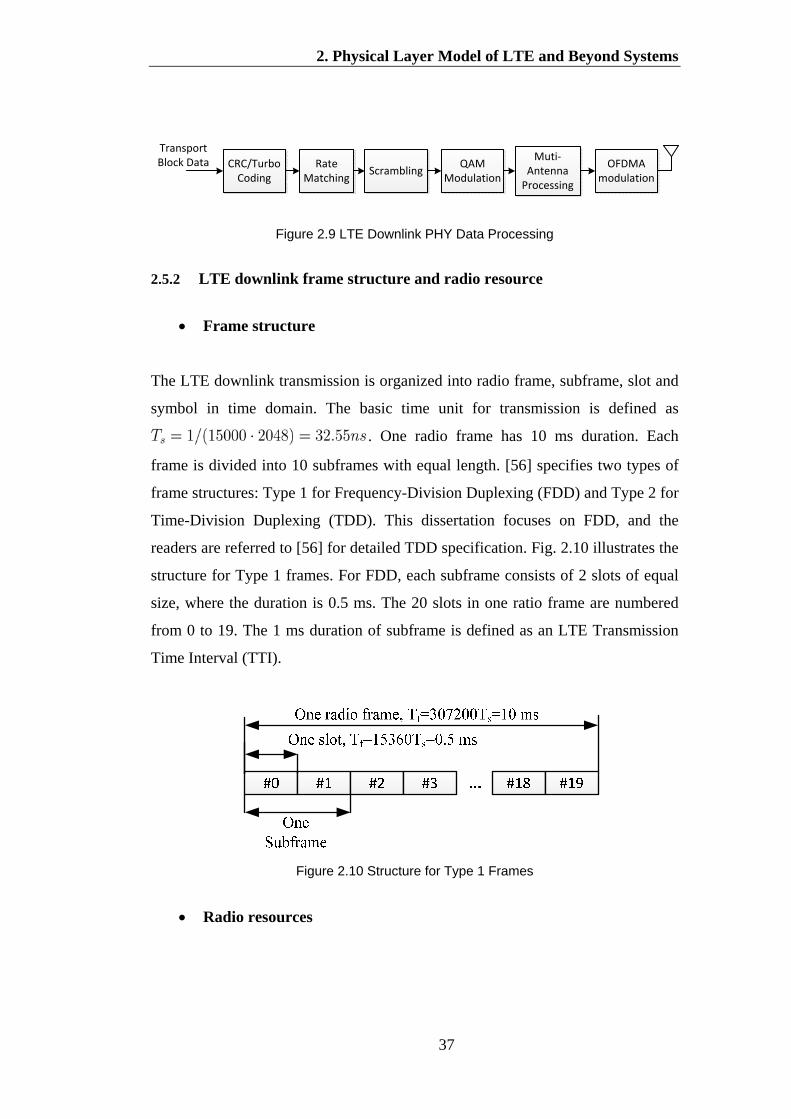
2. Physical Layer Model of LTE and Beyond Systems
37
CRC/Turbo Coding
Rate Matching
ScramblingQAM
Modulation
Muti-AntennaProcessing
OFDMA modulation
Transport Block Data
Figure 2.9 LTE Downlink PHY Data Processing
2.5.2 LTE downlink frame structure and radio resource
Frame structure
The LTE downlink transmission is organized into radio frame, subframe, slot and
symbol in time domain. The basic time unit for transmission is defined as
. One radio frame has 10 ms duration. Each
frame is divided into 10 subframes with equal length. [56] specifies two types of
frame structures: Type 1 for Frequency-Division Duplexing (FDD) and Type 2 for
Time-Division Duplexing (TDD). This dissertation focuses on FDD, and the
readers are referred to [56] for detailed TDD specification. Fig. 2.10 illustrates the
structure for Type 1 frames. For FDD, each subframe consists of 2 slots of equal
size, where the duration is 0.5 ms. The 20 slots in one ratio frame are numbered
from 0 to 19. The 1 ms duration of subframe is defined as an LTE Transmission
Time Interval (TTI).
Figure 2.10 Structure for Type 1 Frames
Radio resources

2. Physical Layer Model of LTE and Beyond Systems
38
The radio resource of LTE is divided into several frequency-time grids. The
smallest frequency-time unit in downlink and uplink is called a Resource Element
(RE). An RE on a specific antenna port is specified as one subcarrier over one
OFDM symbol. Hence, one RE corresponds to one modulated complex data. The
mapping of LTE physical channels to resource elements is described by resource
blocks (RBs). A physical resource block consists of 12 consecutive subcarriers in
a frequency domain over one slot (0.5 ms) in time domain. The subcarrier spacing
is specified as 15 or 7.5 KHz. Thus one RB occupies radio
resource in frequency and time domain respectively. The LTE provides 6 different
transmission bandwidths by enabling a different amount of RB, which ranges
from 6 to 100 RBs and corresponds to a bandwidth of 1.4 MHz to 20 MHz. All
the available subcarriers in the full bandwidth over one slot consist of one
resource grid. Fig. 2.11 shows the general structure of RB and the resource grid.
The total number of RB within the available downlink bandwidth is denoted by
; the number of subcarriers and symbols in one resource block is denoted by
and respectively.
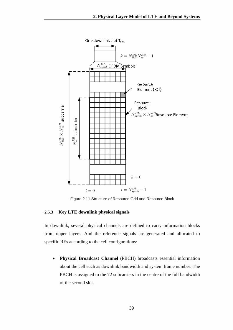
2. Physical Layer Model of LTE and Beyond Systems
39
(k; l)(k; l)
Figure 2.11 Structure of Resource Grid and Resource Block
2.5.3 Key LTE downlink physical signals
In downlink, several physical channels are defined to carry information blocks
from upper layers. And the reference signals are generated and allocated to
specific REs according to the cell configurations:
Physical Broadcast Channel (PBCH) broadcasts essential information
about the cell such as downlink bandwidth and system frame number. The
PBCH is assigned to the 72 subcarriers in the centre of the full bandwidth
of the second slot.

2. Physical Layer Model of LTE and Beyond Systems
40
Primary and Secondary Synchronization Signal (PSS and SSS) are
located in the first subframe of the radio frame. These two signals enable
the users to be synchronized on a subframe level and to obtain cell
information.
Physical Downlink Shared Channel (PDSCH) carries the user data
which is dynamically assigned to the REs Multimedia Broadcast and
Multicast Services.
Reference signal is used for time-frequency synchronization and channel
estimation. LTE defines three types of reference signal: cell specific, UE
specific and broadcast specific RS. This dissertation focuses on the cell
specific reference signal. The reference signal is generated from the Gold
sequence based on the cell ID.
This dissertation investigates algorithms based on the above channels and
reference signal. For other control and transport channels readers are referred to
[56].
2.5.4 LTE eICIC scheme
In order to improve the spectral efficiency per unit area, LTE proposes
Heterogeneous Networks (HetNet) topologies which consist of macro cells and
smaller pico/femto cells as shown in Fig. 2.12. The macro cell provides wide area
coverage and serves a larger amount of UEs. The pico/femto cells fulfil the
network needs, and improve spectral efficiency and capacity. However, this multi-
layer topology also encounters an interference problem. As Fig. 2.12 shows, the
UEs will adhere to a pico/femto cell if it is within the coverage of these cells.
However, these UEs can still receive a signal from macro cell when it is within
the coverage of macro cell. The signal from macro cell causes interference to
pico/femto-UEs. To mitigate this inter-cell interference, LTE Release 10 [67]
proposes a time domain enhanced inter-cell interference cancellation (eICIC)
scheme using almost blank subframes (ABS). During ABS, the macro cell is

2. Physical Layer Model of LTE and Beyond Systems
41
scheduled to switch off PDSCH and only transmits essential signals such as CRS,
PSS and SSS. Fig 2.17 shows a basic principle of ABS frame. The ABS frames,
as shown in the while region of Fig. 2.13, do not carry PDSCH signal. This
implies that the pico/femto-UEs will not be dominated by interference from macro
cells. However, the remaining signals in the ABS still cause interference [54].
Further eICIC (FeICIC) will be proposed in the coming Release 12. Hence, this
dissertation investigates algorithms that can suppress residual CRS interference
for FeICIC.
Figure 2.12 Heterogeneous Network
Figure 2.13 Basic Principle of ABS

42
3. Self-IQ-demodulation based FD I/Q Imbalance Compensation
A low cost FD (FD) I/Q imbalance self-compensation scheme is investigated in
this chapter. Direct conversion transmitters are widely used in wireless systems.
However, unwanted image-frequencies and distortions are inevitably introduced
into direct conversion systems. This problem is even more severe in wideband
systems. Therefore, accurate estimation and compensation of I/Q imbalance is
crucial. The current compensation method is based on external instruments or an
internal feedback path which introduces additional impairments and is expensive.
This chapter proposes a low cost FD I/Q imbalance self-IQ-demodulation based
compensation scheme without using external calibration instruments. First, the
impairments of baseband and RF components are investigated. Further to this, an
I/Q imbalance model is developed. Then, the proposed two-step self-IQ-
demodulation based compensation scheme is investigated. In the first step of the
scheme, the local oscillator (LO) related I/Q impairment parameters are estimated.
Then in the second step, the overall FD I/Q imbalance parameters are estimated
by utilizing the transmitter LO. To realize this self-IQ-demodulation algorithm,
minor modifications are introduced to the current power detector circuit.
Afterwards, the estimated parameters are applied to the baseband equivalent
compensator. This sophisticated algorithm guarantees low computation
complexity and low cost. The compensation performance is evaluated using
laboratory measurement.
3.1 Introduction
Direct-conversion transmitters (DCT) are widely adopted in digital broadcasting
systems such as digital audio broadcasting (DAB), digital video broadcasting
(DVB), and digital terrestrial multimedia broadcasting (DTMB) because of the

3. Self-IQ-Demodulation Based FD I/Q Imbalance Compensation
43
advantages of low-cost, simplicity and flexibility. The ideal digital complex signal
is represented by inphase and quadrature signal in the I and Q branch respectively.
The baseband I and Q signal is then modulated by a quadrature modulator which
makes DCT easy to implement. However, some practical problems arise from the
implementation of direct-conversion transmitters. These problems are mainly
caused by the non-idealities of the baseband and RF components, such as I/Q
imbalance, clock jitter, power amplifier (PA) distortion and inter-modulation. The
overall impact results in image-frequency interference, phase noise and high order
frequency interference, which severely degrades the transmitter performance
especially for wideband multicarrier systems. Generally, the main impact of I/Q
imbalance is image-frequency interference and degradation of PA nonlinearity [18,
68-70]. In OFDM systems such as DVB, the image frequency component
overlaps the desired signal on corresponding subcarriers, which decreases the
SNR of the desired signal. Hence, image rejection ratio (IRR) is a critical criterion
for DCT.
There are several works covered in the literature. The work in [71] addresses the
combined effects of transmitter and receiver I/Q imbalance, whereas, the work in
[18, 26, 72] focuses on transmitter I/Q imbalance and adopts a low intermediate
frequency (IF) down-conversion structure, in which the corrupted signal is down-
converted to a low IF and sample with an analog-to-digital converter (ADC),
which requires a high speed ADC. I/Q demodulation and parameters estimation
are computed by DSP. The advantage of this estimation structure is that I/Q
demodulation is performed in the digital domain, which avoids the receiver I/Q
imbalance. [22, 24, 29] also investigates the low-cost diode-based I/Q imbalance
estimation technique, which makes use of the power detector of transmitters and
realizes self-calibration. However, the estimation is confined to FD I/Q imbalance
due to the bandwidth limit of the power detector. [18, 26, 72] studies FD I/Q
imbalance, which is more realistic for wideband systems such as DVB and LTE.
[18] proposes a second-order statistics-based approach and a widely linear least-
squares (WL-LS) approach. These do not take LO leakage into account. [26]
estimates I/Q imbalance parameters by cross-processing between I and Q signals.

3. Self-IQ-Demodulation Based FD I/Q Imbalance Compensation
44
[72] proposes a specially designed pilot sequence, which estimates I/Q imbalance
and channel response jointly. Recently, [73] proposed a diode based IQ imbalance
and nonlinearity method. A joint model of IQ imbalance and nonlinear is
analytically derived. Special test signals are devised to isolate the effects of gain
and phase imbalance, dc offsets. Based on this isolation, the imbalance and
nonlinearity are calculated easily with a few mathematical operations. However,
this method is only applied to frequency-independent scenarios.
In this dissertation, a self-IQ-demodulation based compensation scheme of FD I/Q
imbalance is studied and presented, as shown in Fig. 3.1. In particular, the “time
division” method and its corresponding circuit are implemented to realize self-IQ-
demodulation. This compensation scheme consists of estimation and
compensation stages. The estimation stage adopts a two-step self-IQ-
demodulation algorithm. In the first step, the amplitude LO impairments,
including DC offset, are estimated using the power detector. Two tone training
signal is transmitted to measure these impairments. This special training signal is
designed with low computation complexity. In the second step, the self-I/Q-
demodulation is implemented to estimate the FD I/Q imbalance parameters. As
the external I/Q demodulator has been omitted in this scheme, the transmitter LO
is transmitted with the test signal using the “time division” method for self-I/Q-
demodulation. The LO related impairments parameters, which are estimated in
Step 1 are then used to compensate the self-I/Q-demodulation error caused by the
inherent transmitter LO imbalance. Afterwards, the FD I/Q imbalance can be
estimated. Furthermore, the estimation results are applied to the compensation
stage. The circuit components in [22, 24, 29] are extended to wideband in this
proposal to meet the requirement of self-I/Q-demodulation.

3. Self-IQ-Demodulation Based FD I/Q Imbalance Compensation
45
f df r¡ f r¡ f df
xI (t)
L OI
xI (t)
L OQ
xQ (t)
L OI
xQ (t)
L OQ
t
St ep 1 :
St ep 2 :
ADCADC
DSPDSP
DCTDCTRFRF
CC
BasebandBaseband
Figure 3.1Proposed Compensation Scheme
3.2 I/Q Imbalance model
LTE adopts complex signal to carry the user and control data. The complex signal
can be presented with a single sideband spectrum in the frequency domain. This
means the complex signal occupies only a single sideband in the range of [0, B]
Hz or [-B, 0] where is a value that specifies the signal bandwidth. In contrast,
the real signal occupies a double sideband in [-B, B] Hz. Hence, a complex signal
improves spectrum efficiency. However, the analog signal in the real word is real
form. There are many methods to represent a complex signal using a real signal,
such as Hilbert Transform, quadrature modulation and Polyphase filtering. This
dissertation focuses on quadrature modulation.
3.2.1 Ideal quadrature modulation
Figure 3.2 Ideal DCT Topology
Quadrature modulation, or direct conversion, is a technique used to construct a
complex signal by mixing baseband signals with quadrature carriers as shown in
Fig. 3.2. Consider a baseband complex signal :
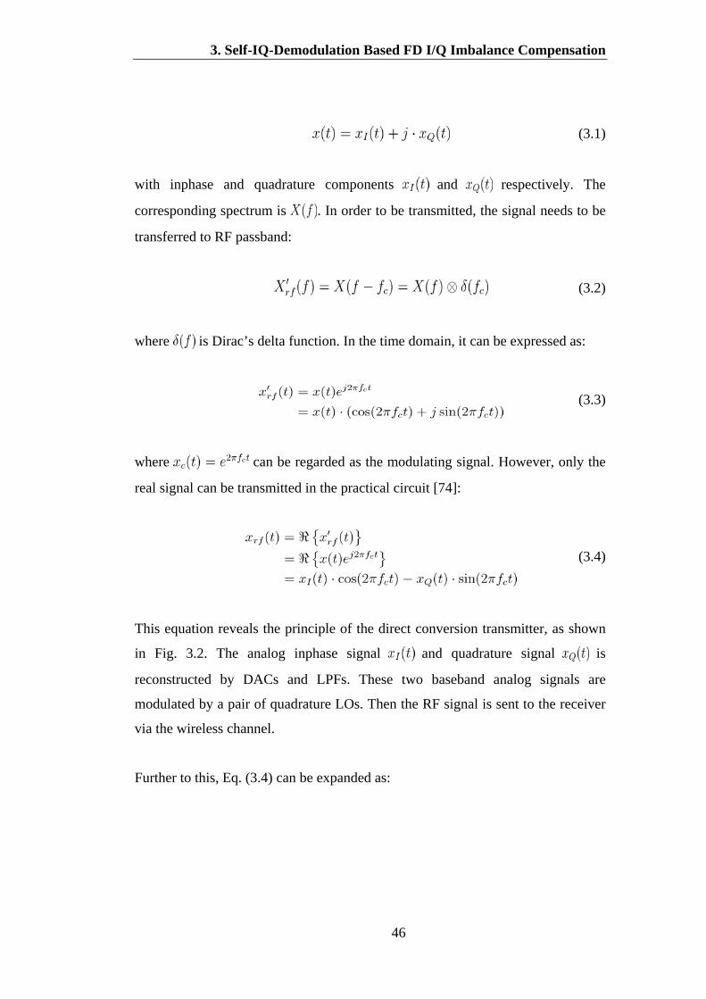
3. Self-IQ-Demodulation Based FD I/Q Imbalance Compensation
46
(3.1)
with inphase and quadrature components and respectively. The
corresponding spectrum is . In order to be transmitted, the signal needs to be
transferred to RF passband:
(3.2)
where is Dirac’s delta function. In the time domain, it can be expressed as:
(3.3)
where can be regarded as the modulating signal. However, only the
real signal can be transmitted in the practical circuit [74]:
(3.4)
This equation reveals the principle of the direct conversion transmitter, as shown
in Fig. 3.2. The analog inphase signal and quadrature signal is
reconstructed by DACs and LPFs. These two baseband analog signals are
modulated by a pair of quadrature LOs. Then the RF signal is sent to the receiver
via the wireless channel.
Further to this, Eq. (3.4) can be expanded as:
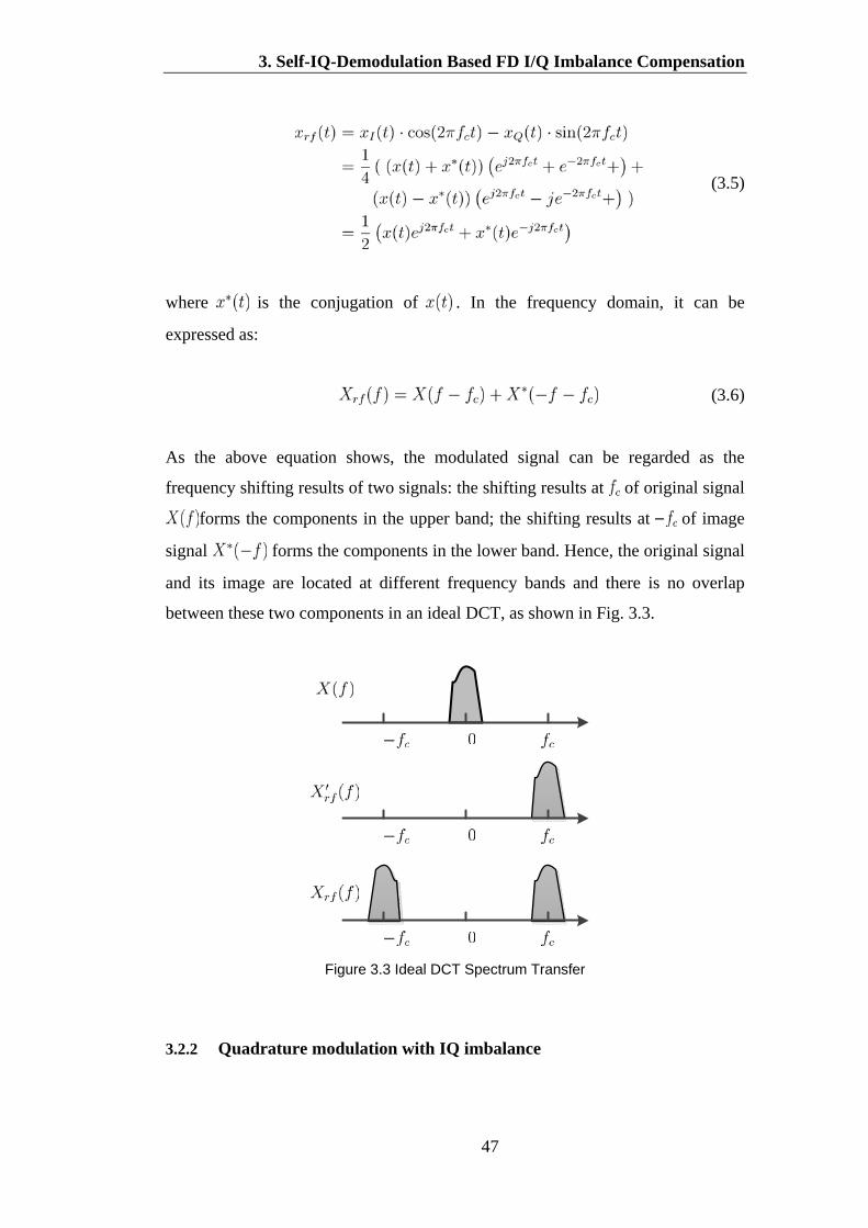
3. Self-IQ-Demodulation Based FD I/Q Imbalance Compensation
47
(3.5)
where is the conjugation of . In the frequency domain, it can be
expressed as:
(3.6)
As the above equation shows, the modulated signal can be regarded as the
frequency shifting results of two signals: the shifting results at of original signal
forms the components in the upper band; the shifting results at of image
signal forms the components in the lower band. Hence, the original signal
and its image are located at different frequency bands and there is no overlap
between these two components in an ideal DCT, as shown in Fig. 3.3.
Figure 3.3 Ideal DCT Spectrum Transfer
3.2.2 Quadrature modulation with IQ imbalance
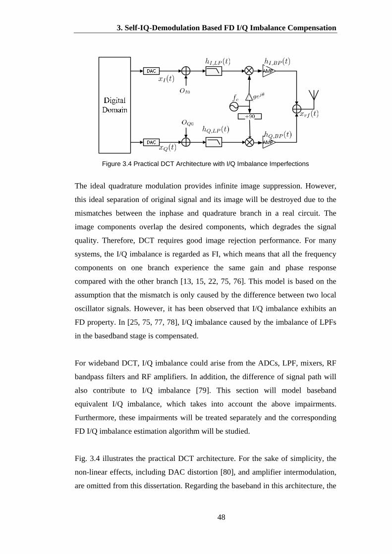
3. Self-IQ-Demodulation Based FD I/Q Imbalance Compensation
48
Figure 3.4 Practical DCT Architecture with I/Q Imbalance Imperfections
The ideal quadrature modulation provides infinite image suppression. However,
this ideal separation of original signal and its image will be destroyed due to the
mismatches between the inphase and quadrature branch in a real circuit. The
image components overlap the desired components, which degrades the signal
quality. Therefore, DCT requires good image rejection performance. For many
systems, the I/Q imbalance is regarded as FI, which means that all the frequency
components on one branch experience the same gain and phase response
compared with the other branch [13, 15, 22, 75, 76]. This model is based on the
assumption that the mismatch is only caused by the difference between two local
oscillator signals. However, it has been observed that I/Q imbalance exhibits an
FD property. In [25, 75, 77, 78], I/Q imbalance caused by the imbalance of LPFs
in the basedband stage is compensated.
For wideband DCT, I/Q imbalance could arise from the ADCs, LPF, mixers, RF
bandpass filters and RF amplifiers. In addition, the difference of signal path will
also contribute to I/Q imbalance [79]. This section will model baseband
equivalent I/Q imbalance, which takes into account the above impairments.
Furthermore, these impairments will be treated separately and the corresponding
FD I/Q imbalance estimation algorithm will be studied.
Fig. 3.4 illustrates the practical DCT architecture. For the sake of simplicity, the
non-linear effects, including DAC distortion [80], and amplifier intermodulation,
are omitted from this dissertation. Regarding the baseband in this architecture, the

3. Self-IQ-Demodulation Based FD I/Q Imbalance Compensation
49
digital signals of inphase and quadrature branches are converted to analog signal
by DACs. In order to limit the signal bandwidth and prevent aliasing, the signals
pass through a pair of reconstruction filters, which have low pass properties. At
this initial data conversion stage, the signal could be influenced by the following
impairments:
1). Amplitude and phase mismatch between two DACs. Due to the voltage
reference difference and clock delay, the output of each DAC is not strictly
matched.
2). Amplitude and phase mismatch between reconstruction filters.
3). DC offset. Due to the voltage reference drift, the output signal contains DC
offset components. Assuming that the reconstruction filter can limit the signal
band to , then the analog signals of the two branches can be
reconstructed with amplitude and phase imbalance. Hence, the mismatch of DAC
along with a low pass reconstruction filter is modelled on the reconstruction filter.
Denoting and as the equivalent impulse response of the
reconstruction filters on the inphase and quadrature branch respectively, the
baseband signals in Eq. (3.1) become:
(3.7)
(3.8)
where, and are the DC offset of inphase and quadrature branch
respectively. As the corrupted signal is still real-valued, the spectrum will be
Hermitian symmetrical about the zero frequency. This means that the amplitudes
for the positive and negative frequency are equal, whereas the phases for the
positive and negative frequency are inverse.
The baseband analog signals will be upconverted to RF frequency band by a pair
of quadrature local oscillators (LO). In practice, the two oscillators contribute
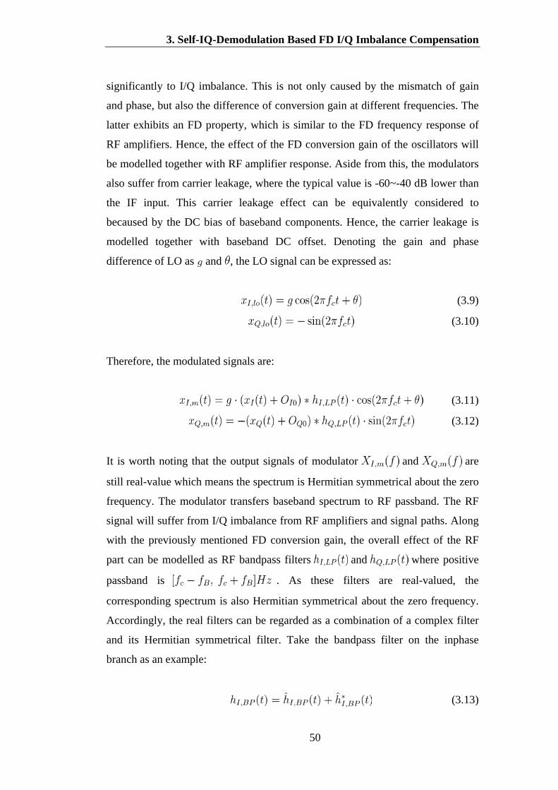
3. Self-IQ-Demodulation Based FD I/Q Imbalance Compensation
50
significantly to I/Q imbalance. This is not only caused by the mismatch of gain
and phase, but also the difference of conversion gain at different frequencies. The
latter exhibits an FD property, which is similar to the FD frequency response of
RF amplifiers. Hence, the effect of the FD conversion gain of the oscillators will
be modelled together with RF amplifier response. Aside from this, the modulators
also suffer from carrier leakage, where the typical value is -60~-40 dB lower than
the IF input. This carrier leakage effect can be equivalently considered to
becaused by the DC bias of baseband components. Hence, the carrier leakage is
modelled together with baseband DC offset. Denoting the gain and phase
difference of LO as and , the LO signal can be expressed as:
(3.9)
(3.10)
Therefore, the modulated signals are:
(3.11)
(3.12)
It is worth noting that the output signals of modulator and are
still real-value which means the spectrum is Hermitian symmetrical about the zero
frequency. The modulator transfers baseband spectrum to RF passband. The RF
signal will suffer from I/Q imbalance from RF amplifiers and signal paths. Along
with the previously mentioned FD conversion gain, the overall effect of the RF
part can be modelled as RF bandpass filters and where positive
passband is . As these filters are real-valued, the
corresponding spectrum is also Hermitian symmetrical about the zero frequency.
Accordingly, the real filters can be regarded as a combination of a complex filter
and its Hermitian symmetrical filter. Take the bandpass filter on the inphase
branch as an example:
(3.13)

3. Self-IQ-Demodulation Based FD I/Q Imbalance Compensation
51
Furthermore, it is easy to construct a complex filter where the non-zero
frequency band is only restricted to with a passband of
is . Equivalently, Eq. (3.13) can be rewritten as:
(3.14)
According to Eq. (3.14), the bandpass filters at the RF passband can be considered
as the frequency shift result of baseband complex filters and
where the corresponding frequency band is constrained to . As
exhibits the same frequency responsewith within the passband,
this dissertation defines as the baseband equivalent of . Similarly,
is defined as the baseband equivalent of :
(3.15)
Consequently, the output corrupted RF signal on inphase and quadrature branch
can be written as:
(3.16)
(3.17)
The final RF signal is the addition of signals from the inphase and quadrature
branches:

3. Self-IQ-Demodulation Based FD I/Q Imbalance Compensation
52
(3.18)
After some mathematic substitutions, the above equation can be rewritten as [81]:
(3.19)
The coefficients in term (a) and (b) are defined as:
(3.20)
(3.21)
where
(3.22)
(3.23)
Consequently, Eq. (3.19) can be rewritten as:

3. Self-IQ-Demodulation Based FD I/Q Imbalance Compensation
53
(3.24)
where is the dc terms caused by dc offset in relation to baseband and carrier
leakage.
The above equation gives an overview of the corrupted signal spectrum.
Comparing Eq. (3.19) with the signal spectrum of ideal DCT in Eq. (3.6) , terms
(a) and (c) represent the desired components around and . It is easy to know
that the coefficients for and are Hermitian symmetrical in
term (a) and (c). Thus, the effect of I/Q imbalance on the desired components can
be regarded as channel processing. This means that, given term (a) and (c), the
original signal can be recovered by channel estimation. However, the term (a) and
(c) cannot be explicitly obtained from Eq. (3.24). This is because the image terms
(b) and (d) overlap the desired components around and . These image
components cause interference with the original signals, as shown in Fig. 3.5.
Therefore, the capability of image suppression is a key performance criterion for
DCTs and it is characterized by image rejection ratio (IRR). The IRR is defined to
be to the logarithm power ratio between the image and desired components:
(3.25)
The typical IRR for general DCT without compensation is around 25~40 dB [18].
As the image components interfere with the desired component, it is essential to
reduce the DCT IRR using the compensation filter. The next two sections will
discuss algorithms for the estimation and the compensation of the above
parameters.
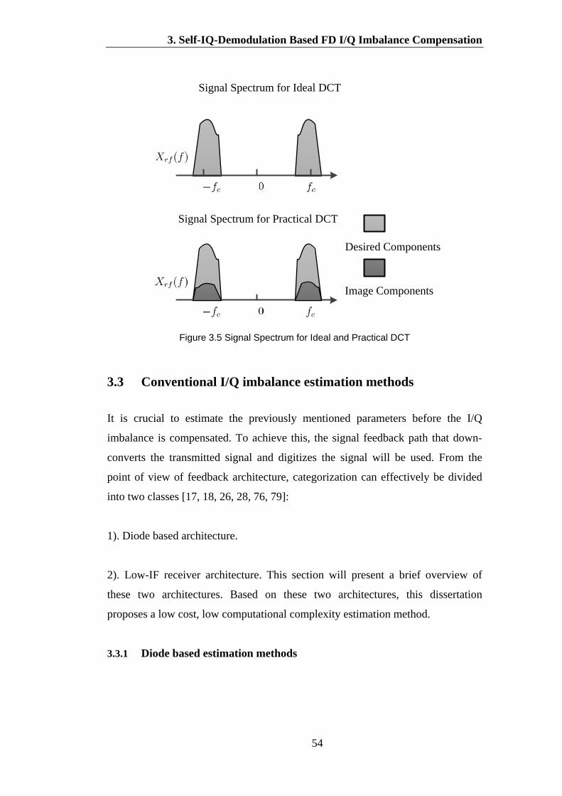
3. Self-IQ-Demodulation Based FD I/Q Imbalance Compensation
54
Desired Components
Image Components
Signal Spectrum for Ideal DCT
Signal Spectrum for Practical DCT
Figure 3.5 Signal Spectrum for Ideal and Practical DCT
3.3 Conventional I/Q imbalance estimation methods
It is crucial to estimate the previously mentioned parameters before the I/Q
imbalance is compensated. To achieve this, the signal feedback path that down-
converts the transmitted signal and digitizes the signal will be used. From the
point of view of feedback architecture, categorization can effectively be divided
into two classes [17, 18, 26, 28, 76, 79]:
1). Diode based architecture.
2). Low-IF receiver architecture. This section will present a brief overview of
these two architectures. Based on these two architectures, this dissertation
proposes a low cost, low computational complexity estimation method.
3.3.1 Diode based estimation methods
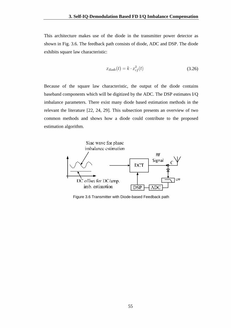
3. Self-IQ-Demodulation Based FD I/Q Imbalance Compensation
55
This architecture makes use of the diode in the transmitter power detector as
shown in Fig. 3.6. The feedback path consists of diode, ADC and DSP. The diode
exhibits square law characteristic:
(3.26)
Because of the square law characteristic, the output of the diode contains
baseband components which will be digitized by the ADC. The DSP estimates I/Q
imbalance parameters. There exist many diode based estimation methods in the
relevant the literature [22, 24, 29]. This subsection presents an overview of two
common methods and shows how a diode could contribute to the proposed
estimation algorithm.
Figure 3.6 Transmitter with Diode-based Feedback path

3. Self-IQ-Demodulation Based FD I/Q Imbalance Compensation
56
Figure 3.7 IQ Imbalance Estimation in Literature [22]
In [22], the author proposes iteratively employing an adjustment algorithm to
estimate the I/Q imbalance. This method assumes the DCT only from LO
imbalance and LO leakage. The LO leakage is estimated by zeroing the input
signal ( ) and then adjusting the DC offset. As shown in Fig. 3.6, DC
offset and sine wave are injected into the DCT. The relationship between input
DC value and output DC value can be easily understood in Fig. 3.7. The optimum
estimate of DC offset is obtained when the output of the diode contains a
minimum of DC components. Similarly, the gain imbalance can be estimated by
transmit adjustable the DC components on I and Q branch: and
, respectively. Then is obtained when the value of and has
the same amplitude. As shown in Fig. 3.7. After amplitude and DC offset the
constant amplitude signal is injected into DCT.
Due to the phase error, the amplitude can is an eclipse function with respect of
input amplitude of I and Q branch. And the phase can be obtained by solve the
output amplitude function and input
function . This method explicitly utilizes Eq.
3. Self-IQ-Demodulation Based FD I/Q Imbalance Compensation
57
(3.26). The RF signal is converted to the baseband by the intermodulation of
carrier and test signal .Then, the imbalance parameters of LO can be directly
estimated using the above methods.
In [29], the author estimates the I/Q imbalance by transmitting a two-tone signal
and calculating the imbalance
parameters by applying a series of matrix operations to the received signal. The
principle behind this method is that the RF signal carrying I/Q imbalance
information is down-converted to the baseband by the intermodulation between
the modulated two tones and carrier. As a result, the tones locate at frequency ,
, , and of the diode output signal will carry I/Q imbalance
information and form solvable equations.
The diode based method provides a low cost estimation solution, which does not
require external calibration instruments and modifications of transmitter internal
circuits. However, these methods mainly assume the DCT only suffers from LO
imbalance and leakage. For wideband systems, it also suffers FD factors such as
imbalanced filters and amplifiers. Therefore low cost diode-based FD I/Q
imbalance estimation algorithms is necessary to be further developed.
3.3.2 LOW-IF based estimation methods
Though quadrature feedback architecture can theoretically estimate I/Q imbalance,
it is rarely used because it actually creates extra I/Q imbalance. A more popular
method is to use a low IF feedback path as shown in Fig. 3.8 [18, 26, 28, 82, 83].
This feedback path can employ external instruments such as a spectrum analyzer
or internal modules.
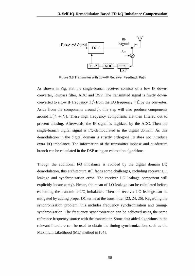
3. Self-IQ-Demodulation Based FD I/Q Imbalance Compensation
58
Figure 3.8 Transmitter with Low-IF Receiver Feedback Path
As shown in Fig. 3.8, the single-branch receiver consists of a low IF down-
converter, lowpass filter, ADC and DSP. The transmitted signal is firstly down-
converted to a low IF frequency from the LO frequency by the converter.
Aside from the components around , this step will also produce components
around . These high frequency components are then filtered out to
prevent aliasing. Afterwards, the IF signal is digitized by the ADC. Then the
single-branch digital signal is I/Q-demodulated in the digital domain. As this
demodulation in the digital domain is strictly orthogonal, it does not introduce
extra I/Q imbalance. The information of the transmitter inphase and quadrature
branch can be calculated in the DSP using an estimation algorithms.
Though the additional I/Q imbalance is avoided by the digital domain I/Q
demodulation, this architecture still faces some challenges, including receiver LO
leakage and synchronization error. The receiver LO leakage component will
explicitly locate at . Hence, the mean of LO leakage can be calculated before
estimating the transmitter I/Q imbalance. Then the receiver LO leakage can be
mitigated by adding proper DC terms at the transmitter [23, 24, 26]. Regarding the
synchronization problem, this includes frequency synchronization and timing-
synchronization. The frequency synchronization can be achieved using the same
reference frequency source with the transmitter. Some data aided algorithms in the
relevant literature can be used to obtain the timing synchronization, such as the
Maximum Likelihood (ML) method in [84].

3. Self-IQ-Demodulation Based FD I/Q Imbalance Compensation
59
The transmitter I/Q imbalance parameters can be estimated based on the
demodulated I/Q data. There are a great number of I/Q-demodulation based
estimation algorithms, such as the second-order statistics-based approach and the
wide linear least square (WL-LS) approach [18]. This subsection will give a brief
overview of WL-LS and explain the principle of the I/Q-demodulation based
estimation methods. The LO leakage estimation details will be found in [29] for
further study.
Eq. (3.24) presents a complete expression for the I/Q imbalanced signal. Omitting
the DC terms, the baseband equivalent model of the imbalanced RF signal is [79]:
(3.27)
And the corresponding time domain expression is:
(3.28)
After being digitized, the observed demodulated signal will take the following
form:
(3.29)
Assuming that the imbalanced filter and have a finite impulse response
and the length of response is , for a segment of observed signal , it can be
expressed in the form of a convolution matrix:
(3.30)
where , is the number of observed
data; and , represents the impulse response of
the imbalanced filters; the convolution matrix has the following form:
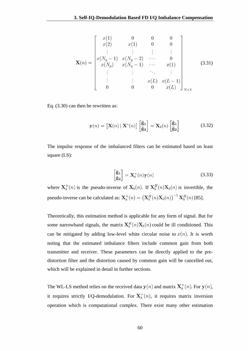
3. Self-IQ-Demodulation Based FD I/Q Imbalance Compensation
60
(3.31)
Eq. (3.30) can then be rewritten as:
(3.32)
The impulse response of the imbalanced filters can be estimated based on least
square (LS):
(3.33)
where is the pseudo-inverse of . If is invertible, the
pseudo-inverse can be calculated as: [85].
Theoretically, this estimation method is applicable for any form of signal. But for
some narrowband signals, the matrix could be ill conditioned. This
can be mitigated by adding low-level white circular noise to . It is worth
noting that the estimated imbalance filters include common gain from both
transmitter and receiver. These parameters can be directly applied to the pre-
distortion filter and the distortion caused by common gain will be cancelled out,
which will be explained in detail in further sections.
The WL-LS method relies on the received data and matrix . For ,
it requires strictly I/Q-demodulation. For , it requires matrix inversion
operation which is computational complex. There exist many other estimation

3. Self-IQ-Demodulation Based FD I/Q Imbalance Compensation
61
methods [18, 26, 72]. These algorithms are based on low-IF single-branch
receivers, as shown in Fig. 3.8. Generally, these architectures are expensive and
heavy in computational complexity.
3.4 Proposed I/Q imbalance estimation method
The previously mentioned estimation methods are constrained by the following
factors: the diode based method is low cost but only applicable for narrowband
DCTs; the low-IF receiver method can deal with FD I/Q imbalance for wideband
DCTs, but is cost ineffective and consumes a lot of computational resources. This
dissertation combines the advantages of these two methods and proposes a self-
I/Q-demodulation compensation scheme which omits the external I/Q
demodulator to reduce the cost.
The self-compensation algorithms in [18, 29, 84] make use of a diode in the
power detector for I/Q imbalance parameter estimation. In these schemes, the RF
signal is self-demodulated by the square law of the diode. However, the
estimation is constrained to FI I/Q imbalance because the diode and ADC can
only cope with narrowband signal. Enlightened by these estimation methods, the
chapter proposes a wideband diode or even a multiplier to be used for FD I/Q
imbalance estimation, as shown in Fig. 3.9. Based on this hardware architecture, a
specific algorithm is required to realize the FD I/Q imbalance estimation.
The reason that the low-IF receiver architecture can cope with the FD I/Q
imbalance is that it utilizes I/Q demodulation and the wideband complex signal
can be recovered accordingly. Whereas in conventional diode based architecture,
the diode only outputs the instantaneous power of the signal, which results in the
loss of the complex information. Therefore, in order to estimate the FD I/Q
imbalance parameters, the proposed wideband diode-based architecture should be
able to realize I/Q demodulation for the transmitted signal. However, the
constraint of this architecture is that this architecture lacks an external
intermediate frequency source for down-conversion. Thus self-I/Q-demodulation
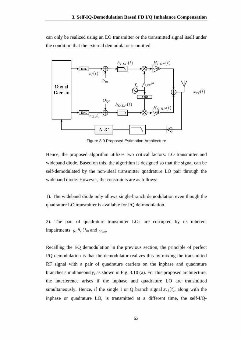
3. Self-IQ-Demodulation Based FD I/Q Imbalance Compensation
62
can only be realized using an LO transmitter or the transmitted signal itself under
the condition that the external demodulator is omitted.
+ 90+ 90
Figure 3.9 Proposed Estimation Architecture
Hence, the proposed algorithm utilizes two critical factors: LO transmitter and
wideband diode. Based on this, the algorithm is designed so that the signal can be
self-demodulated by the non-ideal transmitter quadrature LO pair through the
wideband diode. However, the constraints are as follows:
1). The wideband diode only allows single-branch demodulation even though the
quadrature LO transmitter is available for I/Q de-modulation.
2). The pair of quadrature transmitter LOs are corrupted by its inherent
impairments: , , and .
Recalling the I/Q demodulation in the previous section, the principle of perfect
I/Q demodulation is that the demodulator realizes this by mixing the transmitted
RF signal with a pair of quadrature carriers on the inphase and quadrature
branches simultaneously, as shown in Fig. 3.10 (a). For this proposed architecture,
the interference arises if the inphase and quadrature LO are transmitted
simultaneously. Hence, if the single I or Q branch signal , along with the
inphase or quadrature LO, is transmitted at a different time, the self-I/Q-

3. Self-IQ-Demodulation Based FD I/Q Imbalance Compensation
63
demodulation of single I or Q branch signal can be achieved with the help of the
square law of the diode. With reference to this, this dissertation realizes I/Q
demodulation by dividing the classical demodulation into two steps: inphase
demodulation and quadrature demodulation, as shown in Fig. 3.10 (b). In the first
step, the inphase carrier and training signal is transmitted. Due to the
intermodulation of the diode, the inphase demodulation can be realized. The
quadrature demodulation is realized in a similar way in which the quadrature
carrier and training signal is transmitted. This method can be viewed as “time
division” realization of I/Q demodulation. The phase delay caused by the “time
division” is cancelled out by the intermodulation and the training signal which
will be shown with further mathematical derivation.
++++
Figure 3.10 I/Q demodulation
Though the “time division” method provides a solution for I/Q demodulation by
using a diode, the constraint of the imbalanced LO will corrupt the demodulated

3. Self-IQ-Demodulation Based FD I/Q Imbalance Compensation
64
signal and introduce additional error. Thus, an accurate estimation of the LO
imbalance , , and is essential to compensate for this error. Accordingly,
the proposed estimation will firstly estimate the LO imbalance. Then the overall
FD I/Q imbalance will be estimated. The estimation process is depicted in Fig.
3.11. As Fig. 3.11 shows, the estimation process will be consisted of 7 steps. In
each step, specific train signal will be transmitted to get the corresponding
measurements. In step 1 and 2, and will be transmitted to estimate the
LO gain imbalance , and DC offset . Then, the imperfection of LO will
be compensated using these estimated values. Afterwards, the LO can be regarded
as ideal and there still exists frequency-dependent imbalance on RF branch. In
steps 4~7, signal ~ will be transmitted to estimate the frequency
imbalance. At last, the overall I/Q imbalance can be obtained.
Figure 3.11Frequency-dependent I/Q Imbalance Estimation Procedure
3.4.1 LO impairments and DC offset estimation

3. Self-IQ-Demodulation Based FD I/Q Imbalance Compensation
65
There exist many diode based LO imbalance estimation methods in the referenced
literature [18, 29, 84]. Apart from the previously mentioned methods, [84]
proposes a measurement approach, which makes use of a diode in the envelope
detector. However it is only suitable for QPSK and Continuous Phase Modulation
(CPM) systems. [18] and [29] proposes estimation methods in generic situations.
In these methods, I/Q imbalance information is obtained from the intermodulation
results between the carriers and test tones. Nonetheless, the computational
complexity is relatively high because of the matrix inversion operation when a
large number of samples are involved.
In this thesis, the LO impairments , , and will be estimated at low
complexity with the help of a specially designed test signal. Consider two tones
that have frequencies and close to each other and are passed through a diode,
as shown in Fig. 3.12 (a) and (b). Due to the square law of the diode, these two
tones intermodulate with each other and this results in tones which are located at
and respectively. Actually, these tones contain the LO
impairments information. If the frequencies and are low enough, the signal is
narrowband and the imbalance parameter can be viewed as FI, which means , ,
and can be obtained from the intermodulation products located at
. In order to achieve this, the test tones are designed so that the tones
that carry the LO impairment information of the inphase and quadrature branches
can be down-converted to baseband, as described in the following steps:
a. Transmit signal where
and in I and Q branch.
The signal spectrum is shown in Fig. 3.12 (a). Omitting the FD effect, the output
signal of the diode can be rewritten as:
(3.34)
where is complex gain and
3. Self-IQ-Demodulation Based FD I/Q Imbalance Compensation
66
(3.35)
Apply FFT to , and the complex gain of the tone at frequency
is:
(3.36)
where is the overall gain of the transmitter and diode.
b. Similarly, transmit the signal where
and . The signal
spectrum is shown in Fig. 3.12 (b) and the complex gain of the output signal at
frequency is
(3.37)
c. Solving Eq. (3.36) and (3.37), we can get:
(3.38)
(3.39)
where and
d. Estimation of DC offset. The DC offset can also be estimated by using the

3. Self-IQ-Demodulation Based FD I/Q Imbalance Compensation
67
Transmit signals where , ;
where , and
where , and is
the DC offset which goes with the sine wave. It should be note that as this method
uses square law model, hence small signal will be applied. Large signal amplitude
of sine wave and DC offset will introduce distortions, which results worse
measurements. Assuming that the I and Q branch have been compensated, then
the complex gain of signal 3, 4 and 5 at frequency can be expressed as:
(3.40)
(3.41)
(3.42)
where
(3.43)
(3.44)
(3.45)
is the path gain.

3. Self-IQ-Demodulation Based FD I/Q Imbalance Compensation
68
Figure 3.12 Signal Spectrum Transfer for Step a and b
The derivation of Eq. (3.36) and (3.37) could be verified by matlab simulation. In
the simulation, the signal will be corrupted by LO related I/Q imbalance factors,
namely, and . Then the corrupted signal will pass through ideal diode model, as
shown in Eq. (3.34).The amplitude of and at interested frequency point
are calculated from the spectrum of diode outpout, which are presented as red
curve as shown in Fig. 3.13. Meanwhile, the amplitude of and at
interested frequency point are calculated from Eq. (3.46) and (3.47), as the blue
curves shown in Fig. 3.13. The impairment factors varies from 0.9 to 1.1 and
is set to 0.1. The generated signal is added noise with SNR 30 dB. As Fig. 3.13
shows, we can find the amplitude of and calculated by derivation and
simulation are very closed, which verifies the correctness of the derivation of Eq.
(3.36) and (3.37).

3. Self-IQ-Demodulation Based FD I/Q Imbalance Compensation
69
Figure 3.13 Amplitude of and Calculated from Derivation and Simulations
3.4.2 FD related I/Q impairment parameters estimation
After estimating the LO impairments, this section can estimate the overall I/Q
imbalance filter and in Eq. (3.20) and (3.21). As presented earlier, the
FD I/Q imbalance parameters can be estimated by using low-IF receiver
architecture. The down-converted signal is digitized by high speed ADC. Then, in
the digital domain, I/Q demodulation is realized with the help of a quadrature LO
pair which are strictly orthogonal. The complex training signal is used in these
methods. The imbalanced parameter carried by the modulated complex signal is
obtained by a self-IQ-demodulation process. Theoretically, the complex training
signal can be applied in the proposed “time division” I/Q demodulation scheme.
0.9 0.92 0.94 0.96 0.98 1 1.02 1.04 1.06 1.08 1.00 1.020.24
0.26
0.28
0.3
0.32
0.34
0.36
0.38
0.4Amplitude of V- 1 Calculated from Derivat ion and Simulat ion
g
V-1
Derivat ion ResultsSimulat ion Results
Simulateion SNR = 30 dB
0.9 0.92 0.94 0.96 0.98 1 1.02 1.04 1.06 1.08 1.00 1.020.3174
0.3175
0.3176
0.3177
0.3178
0.3179
0.318
0.3181
0.3182
0.3183Amplitude of V- 2 Calculated from Derivat ion and Simulat ion
g
V-2
Derivat ion ResultsSimulat ion Results
Simulateion SNR = 30 dB

3. Self-IQ-Demodulation Based FD I/Q Imbalance Compensation
70
However, the complex signal is not essential to the whole process. Effectively,
only the desired branch will transmit a training signal when the imbalanced filter
of this branch is being estimated and another branch is “switched off”. In other
words, a real-valued signal instead of a complex-valued training signal will be
used in this method. Though the conventional complex training signal can also be
used, the real training signal outperforms the complex training signal, which will
be shown in the simulation.
In addition, the conventional wideband training signal causes interference with
itself when passing through the diode. Thus, the proposed estimation will adopt a
single tone signal as a training signal. The wideband I/Q imbalance can be
estimated at each frequency point within the band of interest. Effectively, the
wideband training signal will severely degrade the estimation performance. This
will be shown later in the laboratory experiment results. As the demodulation is
“time division” and a real-valued training signal is only used, the “time division”
I/Q demodulation can be divided into four steps, as shown in Table 3.1.
Table 3.1 “time division” I/Q Demodulation Process “Time Division” Process Corresponding
Transmitted Signal
1. Inphase demodulation for inphase branch signal
2. Quadrature demodulation for inphase branch signal
3. Inphase demodulation for quadrature branch signal
4. Quadrature demodulation for quadrature branch signal
As the carrier leakage can be easily compensated using the estimation results from
Section 3.4.1, this section will assume that the carrier leakage is already
compensated and it omits the carrier leakage term in the mathematic derivation.
The period of training signal in each step is equally set to . The detailed “time
division” I/Q demodulation estimation process is presented as follows:
3.4.3 Inphase demodulation for inphase branch signal
In order to estimate the imbalanced filter on the inphase branch at an frequency of

3. Self-IQ-Demodulation Based FD I/Q Imbalance Compensation
71
interest , the test tones will be transmitted on the inphase branch while the
inphase and quadrature LO will also be transmitted by setting a DC offset as
depicted in Section 3.4.3 and 3.4.4.
In this step, the test tones and LO will be transmitted on the inphase branch. Set
the test tone as: where and
in the first signal period . Eq. (3.18) can be rewritten as:
(3.48)
In the frequency domain, Eq. (3.48) can be written as:
(3.49)
where is the baseband equivalent imbalanced filter
on the inphase branch.
According to Eq. (3.49), the output signal of the diode in the frequency domain
will be:
(3.50)
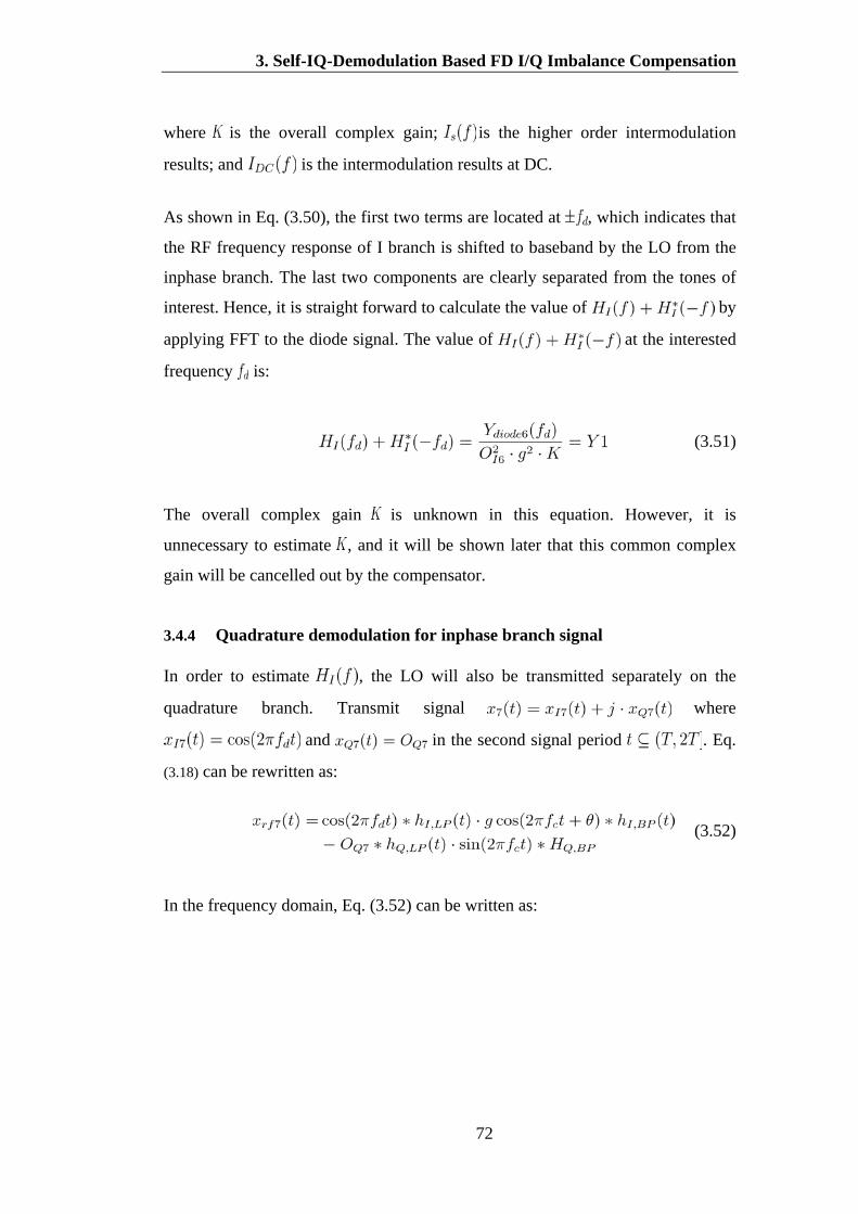
3. Self-IQ-Demodulation Based FD I/Q Imbalance Compensation
72
where is the overall complex gain; is the higher order intermodulation
results; and is the intermodulation results at DC.
As shown in Eq. (3.50), the first two terms are located at , which indicates that
the RF frequency response of I branch is shifted to baseband by the LO from the
inphase branch. The last two components are clearly separated from the tones of
interest. Hence, it is straight forward to calculate the value of by
applying FFT to the diode signal. The value of at the interested
frequency is:
(3.51)
The overall complex gain is unknown in this equation. However, it is
unnecessary to estimate , and it will be shown later that this common complex
gain will be cancelled out by the compensator.
3.4.4 Quadrature demodulation for inphase branch signal
In order to estimate , the LO will also be transmitted separately on the
quadrature branch. Transmit signal where
and in the second signal period . Eq.
(3.18) can be rewritten as:
(3.52)
In the frequency domain, Eq. (3.52) can be written as:
3. Self-IQ-Demodulation Based FD I/Q Imbalance Compensation
73
(3.53)
According to Eq. (3.53), the output signal of the diode in the frequency domain
will be:
(3.54)
where is the overall complex gain; is the higher order intermodulation
results; and is the intermodulation results at DC.
As shown in Eq. (3.54), the first two terms are located at , which indicates that
the RF frequency response of I branch is shifted to baseband by the LO from the
inphase branch. The last components are clearly separated from the interested
tones. Hence, it is straightforward to calculate the value of
by applying FFT to the diode signal. The value of
at the interested frequency is:
(3.55)
Section 3.4.3 and 3.4.4 provides the method with which to estimate the

3. Self-IQ-Demodulation Based FD I/Q Imbalance Compensation
74
imbalanced filter on the inphase branch; the next sections will present the method
to estimate the imbalanced filter on the quadrature branch.
3.4.5 Inphase demodulation for quadrature branch signal
In order to estimate , the LO will also be transmitted separately on the
inphase branch first. Transmit signal where
and in the second signal period .
Eq. (3.28) can be rewritten as:
(3.56)
In the frequency domain, Eq. (3.56) can be written as:
(3.57)
According to Eq. (3.57), the output signal of the diode in the frequency domain
will be:
(3.58)
where is the overall complex gain; is the higher order intermodulation
results; and is the intermodulation results at DC.
3. Self-IQ-Demodulation Based FD I/Q Imbalance Compensation
75
As shown in Eq. (3.58), the first two terms locates at , which indicates that the
RF frequency response of I branch is shifted to baseband by the LO from inphase
branch. The last components are clearly separated with the interested tones. Hence,
it is straight forward to calculate the value of by
applying FFT to the diode signal. The value of at the
interested frequency is:
(3.59)
3.4.6 Quadrature demodulation of signal from Q branch
In order to estimate , the LO will also be transmitted separately on the
quadrature branch. Transmit signal where
and in the second signal period . Eq.
(3.18) can be rewritten as:
(3.60)
In the frequency domain, Eq. (3.60) can be written as:
(3.61)
According to Eq. (3.61), the output signal of the diode in the frequency domain
will be:

3. Self-IQ-Demodulation Based FD I/Q Imbalance Compensation
76
(3.62)
where is the overall complex gain; is the higher order intermodulation
results; and is the intermodulation results at DC.
As shown in Eq. (3.62), the first two terms locate at , which indicates that the
RF frequency response of I branch is shifted to baseband by the LO from the
inphase branch. The last components are clearly separated from the interested
tones. Hence, it is straightforward to calculate the value of by
applying FFT to the diode signal. The summation of at the
interested frequency is:
(3.63)
Solve Eq. (3.51), (3.55), (3.59) and (3.63) by using the previously estimated and
in Eq. (3.38) and (3.39). The frequency response of and at
can be calculated as follows:
(3.64)
(3.65)
(3.66)
(3.67)
3. Self-IQ-Demodulation Based FD I/Q Imbalance Compensation
77
where ; ;
;
The coefficient in Eq. (3.20) and (3.21) is estimated as:
(3.68)
(3.69)
The “time division” method realizes self-IQ-demodulation and achieves
imbalanced information from the I and the Q branch. According to the above
equations, the overall complex gain is still unknown. However, it is not
necessarily required if the compensator is carefully designed. The design details
are presented later. Recalling Eq. (3.26) the proposed method is based on the
assumption that the square law device is working in ideal conditions. In the real
world scenario, the 3rd and other higher order intermodulation terms produce
interference. This higher order intermodulation produces rich components. It
results in interference with the LO and the signal of interest, which actually
jeopardizes the overall estimation performance. Hence, the simplified training
signal with only one tone produces the least interference and yields the most
accurate estimation results. The performance of one tone and multi-tones are
verified in simulation and laboratory experimental results.
The summary of the whole self-I/Q-demodulation based estimation process is
shown below:

3. Self-IQ-Demodulation Based FD I/Q Imbalance Compensation
78
Figure 3.14 Self-I/Q-demodulation based Estimation Process
3.5 Frequency I/Q imbalance pre-distortion technique
In this section, the baseband pre-distorter will be derived. Eq. (3.27) in Section
3.3.2 gives the baseband equivalent output of the quadrature modulator:
(3.70)
where and are the coefficients defined in Eq. (3.20) and (3.21). In
this equation, the image term is caused by I/Q imbalance and is
undesired which means the pre-distorter should be able to minimize the
coefficients of . Take the pre-distorter form in [86]:
(3.71)
where denotes the pre-distorter frequency distorter. Feed this pre-distorted
signal into the DCT, and the output becomes:
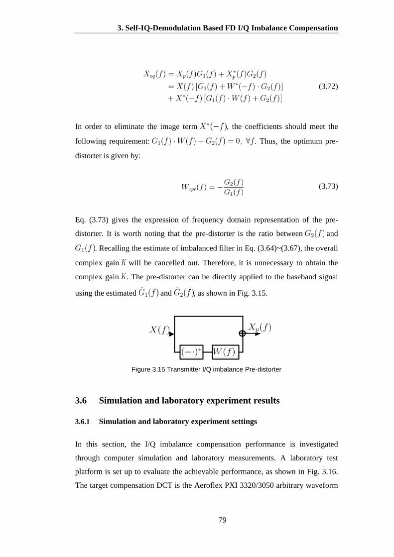
3. Self-IQ-Demodulation Based FD I/Q Imbalance Compensation
79
(3.72)
In order to eliminate the image term , the coefficients should meet the
following requirement: . Thus, the optimum pre-
distorter is given by:
(3.73)
Eq. (3.73) gives the expression of frequency domain representation of the pre-
distorter. It is worth noting that the pre-distorter is the ratio between and
. Recalling the estimate of imbalanced filter in Eq. (3.64)~(3.67), the overall
complex gain will be cancelled out. Therefore, it is unnecessary to obtain the
complex gain . The pre-distorter can be directly applied to the baseband signal
using the estimated and , as shown in Fig. 3.15.
Figure 3.15 Transmitter I/Q imbalance Pre-distorter
3.6 Simulation and laboratory experiment results 3.6.1 Simulation and laboratory experiment settings
In this section, the I/Q imbalance compensation performance is investigated
through computer simulation and laboratory measurements. A laboratory test
platform is set up to evaluate the achievable performance, as shown in Fig. 3.16.
The target compensation DCT is the Aeroflex PXI 3320/3050 arbitrary waveform

3. Self-IQ-Demodulation Based FD I/Q Imbalance Compensation
80
generator. Its bandwidth can be 80 MHz with a typical IRR of about -40~-35 dB.
And there is an internal diode for power control, as shown in Fig. 3.16. In this
experiment, this diode is used to measure the LO imbalance. As the passband of
the target DCT diode is 0-2Mhz, the estimation process for the wideband I/Q
imbalance parameters is emulated using the digitized RF output of PXI 3320/3050:
The output RF signal is directly digitized by a Tektronix oscilloscope 6804B with
8 bit resolution at a sampling rate of 10 GSPS. The digitized RF signal is then
uploaded to a PC. The PC simulates the diode process and estimates the FD I/Q
imbalance using the proposed algorithm. The Aeroflex spectrum analyser is used
to observe the IRR performance. Note that the LO impairments , and DC offset
, is estimated using the internal diode as it meets the narrow band
estimation requirements.
xp(t)xp(t)
xr f (t)xr f (t)
xr f (n)xr f (n)
Figure 3.16 Laboratory Experiment Configuration
3.6.2 Estimation of LO impairments
The estimation performance in Section 3.4.1 is presented in Fig. 3.17 (a), (b) and
Table 3.2. This step aims to estimate LO impairments , and DC offset , .
Since these parameters are FI, the narrowband test tones and

3. Self-IQ-Demodulation Based FD I/Q Imbalance Compensation
81
are used to verify the estimation performance in Section 3.4.1.
According to Fig. 3.17 (a), (b), the estimation algorithm yields nearly 80 dB IRR
which proves the effectiveness of the proposed LO impairments estimation
algorithm.
Table 3.2 also lists the achievable performance for different bandwidths. Carrier
frequency of 2 and 4 GHz is transmitted to verify the effectiveness at different
frequency band. Also, test tones with different offset frequency are transmitted to
verify estimation performance at different signal bandwidth. The signal bandwidth
varies from 500 to 5000 KHz, which represented that the signal varies from
relatively narrow band to wideband. According to the table, the IRR decreases as
the bandwidth increases from 500 to 5000 KHz, which indicates that the FD factor
has a large impact as bandwidth increasesg. It also shows that achievable
performance decreases as bandwidth increases, which indicates that FD
impairments play a more important role in wider band scenarios. In addition, the
IRR performance with the same signal bandwidth at different carrier frequency is
similar, which indicates that this method is suitable for verities of carries
frequency.
(a) 20 KHz upper band signal before FI I/Q imbalance compensation
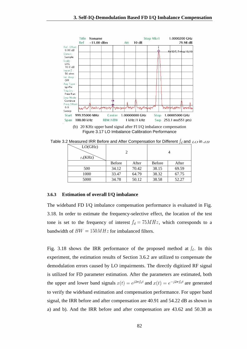
3. Self-IQ-Demodulation Based FD I/Q Imbalance Compensation
82
(b) 20 KHz upper band signal after FI I/Q imbalance compensation
Figure 3.17 LO Imbalance Calibration Performance
Table 3.2 Measured IRR Before and After Compensation for Different and in LO(GHz)
(KHz)
2 4
Before After Before After 500 34.12 70.42 38.15 69.59 1000 33.47 64.79 38.32 67.75 5000 34.78 50.12 38.58 52.27
3.6.3 Estimation of overall I/Q imbalance
The wideband FD I/Q imbalance compensation performance is evaluated in Fig.
3.18. In order to estimate the frequency-selective effect, the location of the test
tone is set to the frequency of interest , which corresponds to a
bandwidth of for imbalanced filters.
Fig. 3.18 shows the IRR performance of the proposed method at . In this
experiment, the estimation results of Section 3.6.2 are utilized to compensate the
demodulation errors caused by LO impairments. The directly digitized RF signal
is utilized for FD parameter estimation. After the parameters are estimated, both
the upper and lower band signals and are generated
to verify the wideband estimation and compensation performance. For upper band
signal, the IRR before and after compensation are 40.91 and 54.22 dB as shown in
a) and b). And the IRR before and after compensation are 43.62 and 50.38 as

3. Self-IQ-Demodulation Based FD I/Q Imbalance Compensation
83
shown in c) and d). It is shown that the proposed estimation algorithm gives more
than 50 dB IRR on both sidebands, which indicates the overall FD I/Q imbalance
in wideband is compensated well
(a) Upper band signal before compensation
(b) Upper band signal after compensation

3. Self-IQ-Demodulation Based FD I/Q Imbalance Compensation
84
(c) Lower band signal before compensation
(d) Lower band signal after compensation
Figure 3.18 Calibration performance at

3. Self-IQ-Demodulation Based FD I/Q Imbalance Compensation
85
Figure 3.19 Compensation performance with varies from 5 to 75 MHz
Fig. 3.19 shows the IRR performance of the proposed method within the whole
signal bandwidth. In this experiment, the estimation results in Section 3.4.2 are
used. In this experiment, a single tone signal is utilized for
estimation. According to this figure, the compensation scheme gives around 10
dB IRR enhancement within bandwidth.
3.6.4 Effect of higher order intermodulation and multi-tone
The previous derivation only considers the square law of the diode, whereas there
exists higher order intermodulation, especially for high transmitting power
scenarios. In this section, the higher order intermodulation of the diode is also
simulated. The actual signal model of the diode in [87] is adopted in this
experiment:
(3.74)
where the coefficients is given in the Appendix A of [88]. The signal amplitude
is set to 500 mV. The simulation results for square model and actual signal model
are shown in Fig. 3.20. The effect of in Eq. (3.50), (3.54), (3.58)and (3.62) is
5 10 15 20 25 30 35 40 45 50 55 60 65 70 7535
40
45
50
55
60
65
70
Frequency(MHz)
IRR
(dB
)
After Compensation, UpperbandAfter Compensation, LowerbandBefore Compensation, UpperbandBefore method, Lowerband
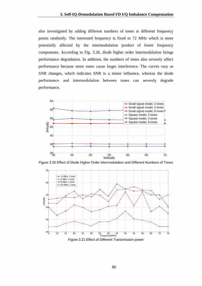
3. Self-IQ-Demodulation Based FD I/Q Imbalance Compensation
86
also investigated by adding different numbers of tones at different frequency
points randomly. The interested frequency is fixed to 72 MHz which is more
potentially affected by the intermodulation product of lower frequency
components. According to Fig. 3.20, diode higher order intermodulation brings
performance degradation. In addition, the numbers of tones also severely affect
performance because more tones cause larger interference. The curves vary as
SNR changes, which indicates SNR is a minor influence, whereas the diode
performance and intermodulation between tones can severely degrade
performance.
Figure 3.20 Effect of Diode Higher Order intermodulation and Different Numbers of Tones
Figure 3.21 Effect of Different Transmission power
40 45 50 55 60 65 7030
35
40
45
50
55
60
SNR(dB)
IRR
(dB
)
Small signal model, 2 tonesSmall signal model, 4 tonesSmall signal model, 8 tonesSquare model, 2 tonesSquare model, 4 tonesSquare model, 8 tones
5 10 15 20 25 30 35 40 45 50 55 60 65 70 7540
45
50
55
60
65
Frequency(MHz)
IRR
(dB
)
-5 dBm, 1 tone0 dBm, 1 tone8 dBm, 1 tone10 dBm, 1 tone
3. Self-IQ-Demodulation Based FD I/Q Imbalance Compensation
87
This effect of higher order intermodulation for single tone signal is also verified
by laboratory measurement, as shown in Fig. 3.21. In this measurement, single
tones with different frequency are transmitted. The figure shows the IRR
performance when the tones are transmitted with different power. It can be shown
that the IRR decreases as the transmit power increases. This is because that the
amplifier produces more higher order harmonics as transmitting power increases.
These harmonics overlap the tones of interest, which degrades the corresponding
signal-to-noise ratio (SNR). However, the most adverse impact is that the
nonlinearity produces a mass of DC components which mixes with the transmitted
DC signal. And the non-linear series model for amplifier could be expressed as:
where is the input to amplifier; is the amplitude output and
are non-linear coefficient, as defined in [81].
As shown in Fig. 3.21, the estimation performance suffers severe degradation
when transmit power is 10 dBm, which is the maximum transmit power of the
PXI 3050, and the amplifier operates in a nonlinear region.The above results is
based on single tone. And multi-tone scenario is not conducted. Obviously, in
multi-tone wideband scenario, the measurement could be much severe. This is
because that multi-tones introduces more intermodulation products, as shown in
Fig. 3.20. Hence, the proposed algorithm is more sensitive to nonlinearity of
amplifier than the conventional method and requires that transmitters operate in
the linear region.
According to Eq. (3.64)~(3.67), the computation complexity of the proposed
algorithm is relatively low, which requires 6 FFT operations and a few
multiplication and addition operations, as compared to the computation
complexity of the conventional low-IF algorithm in Section 3.3.2, which requires
matrix inverse operations and is . As to the cost, this proposed algorithm
only requires a wideband diode and ADC, which is more cost effective than the

3. Self-IQ-Demodulation Based FD I/Q Imbalance Compensation
88
conventional method, which uses an external/internal modulator or even external
instruments.
3.7 Conclusions
This chapter proposes a self-I/Q-demodulation based compensation scheme of FD
I/Q imbalance without using external estimation instruments. Based on the
existing diode-based narrow band compensation scheme, minor modification will
need to be made on the internal power detection circuit to estimate FD I/Q
imbalance parameters. The LO impairments , and DC offset , are
estimated first. Based on these results, the estimator makes use of the LO
transmitter and realizes self-I/Q- demodulation using a “time division” method.
Afterwards, the FD parameters are estimated. The corresponding compensator is
also presented. The performance is verified by laboratory measurements, which
reveal the effectiveness of the compensation scheme. The computation complexity
is relatively low and the implementation cost is low as only a wideband diode and
ADC are required compared with the conventional scheme that requires an
external demodulator and high speed ADCs. It should be note that this scheme is
only suit for signel tone measurement. There will be limitations for multi-tones
measurements due to the intermodulation and non-linear effects.

89
4. MMSE-DFE based OFDM Receiver Algorithm
This chapter introduces a hybrid receiver algorithm that utilizes a pilot-aided
channel estimation method with a decision feedback equalizer (DFE) for OFDM
systems. This receiver algorithm consists of two parts: coarse frequency offset and
channel estimation, and fine frequency estimation. For the coarse estimation, a
joint classical estimation algorithm including carrier frequency offset (CFO) and
channel frequency response (CFR) estimation are used. With the CP of the OFDM
signal and pilot tones in the frequency domain, the dominant CFO, channel effect
is alleviated. The channel estimation in a mobile environment is achieved by
using channel interpolation. Fine estimation presents a pilot-aided residual
frequency offset estimation algorithm, which takes into account the imperfect
channel estimation and Doppler effect. A DFE based on minimum mean squared
error (MMSE) criteria is proposed to cope with the residual ICI and this reduces
the computational burden compared with conventional MMSE-DFE. Further to
this, a FPGA based co-simulation platform is developed. Simulation results
indicate that the proposed hybrid receiver algorithm gives good performance.
4.1 Introduction
As a mature and well-established wireless communication technology, the
Orthogonal Frequency Division Multiplex (OFDM) scheme has been adopted by
LTE downlink chain. The major advantage of an OFDM system is that it makes
efficient use of the spectrum by allowing overlap and is more resistant to
frequency selective fading than single carrier systems. The disadvantage is that it
is more sensitive to carrier frequency offset and drift. The received OFDM signal
is sensitive to synchronization errors: Symbol timing offset (STO), CFO, Sample
frequency offset (SFO) and Doppler shifts [39]. The STO results in phase rotation
on each subcarrier, which can be tolerated to some extent with the help of CP [89].

4. MMSE-DFE Based OFDM Receiver Algorithm
90
The frequency offset destroys the orthogonality in the subcarrier which results in
ICI. For example, frequency offsets of more than 4% of the subcarrier spacing can
result in signal-to-interference ratio (SIR) degradation of 20 dB [90]. And this is
even more severe for systems which have a large number of subcarriers, such as
LTE, DVB. As described in Chapter 2, the double selective channel deteriorates
the signal. The cross influences of these above factors make it difficult to estimate
and compensate purely for a single factor.
Therefore, it is necessary to develop a hybrid synchronization and channel
estimation algorithm to improve the error performance and channel capacity in the
OFDM system. A large amount of investigations have been conducted regarding
OFDM systems. CFO compensation has been studied in the works of [37, 91, 92],
all of which propose both frequency and time domain estimation algorithms. The
channel estimation algorithm [93, 94] introduces blind estimation approaches
which form a relatively complex structure, while [95, 96] investigate data-aided
channel estimation methods which exhibit good performance. Most of the
algorithms on SFO estimation are based on pilot-aid methods or training sequence
[97, 98]. The least mean-square (LMS) error adaptive equalization scheme is
presented in [99]. Two main structures are developed: linear equalizer and
nonlinear equalizer. In [63, 100], zero forcing (ZF) and MMSE criteria are
introduced. In [39, 40], the author systematically analyzes the relevant nonideal
transmission conditions, e.g., STO, CFO, SFO, and doubly selective channel. An
equivalent signal model which contains these nonideal effects is formulated. This
model shows the importance of time and frequency synchronization and acts as a
good reference point for OFDM system design. In [36], a joint estimation and
tracking algorithm for channel response, sampling and carrier frequency offset is
proposed. The channel and frequency offset is estimated jointly and recursively by
optimizing the cost function, which is computationally heavy. It is expected that a
hybrid channel estimation algorithm with DFE structure will enhance error vector
magnitude (EVM) performance.
The objective of this chapter is to develop synchronization and a hybrid pilot-
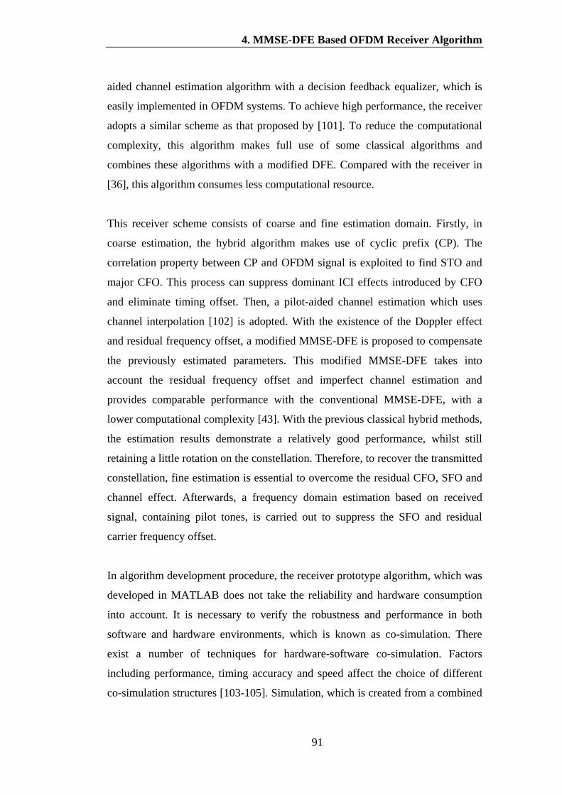
4. MMSE-DFE Based OFDM Receiver Algorithm
91
aided channel estimation algorithm with a decision feedback equalizer, which is
easily implemented in OFDM systems. To achieve high performance, the receiver
adopts a similar scheme as that proposed by [101]. To reduce the computational
complexity, this algorithm makes full use of some classical algorithms and
combines these algorithms with a modified DFE. Compared with the receiver in
[36], this algorithm consumes less computational resource.
This receiver scheme consists of coarse and fine estimation domain. Firstly, in
coarse estimation, the hybrid algorithm makes use of cyclic prefix (CP). The
correlation property between CP and OFDM signal is exploited to find STO and
major CFO. This process can suppress dominant ICI effects introduced by CFO
and eliminate timing offset. Then, a pilot-aided channel estimation which uses
channel interpolation [102] is adopted. With the existence of the Doppler effect
and residual frequency offset, a modified MMSE-DFE is proposed to compensate
the previously estimated parameters. This modified MMSE-DFE takes into
account the residual frequency offset and imperfect channel estimation and
provides comparable performance with the conventional MMSE-DFE, with a
lower computational complexity [43]. With the previous classical hybrid methods,
the estimation results demonstrate a relatively good performance, whilst still
retaining a little rotation on the constellation. Therefore, to recover the transmitted
constellation, fine estimation is essential to overcome the residual CFO, SFO and
channel effect. Afterwards, a frequency domain estimation based on received
signal, containing pilot tones, is carried out to suppress the SFO and residual
carrier frequency offset.
In algorithm development procedure, the receiver prototype algorithm, which was
developed in MATLAB does not take the reliability and hardware consumption
into account. It is necessary to verify the robustness and performance in both
software and hardware environments, which is known as co-simulation. There
exist a number of techniques for hardware-software co-simulation. Factors
including performance, timing accuracy and speed affect the choice of different
co-simulation structures [103-105]. Simulation, which is created from a combined

4. MMSE-DFE Based OFDM Receiver Algorithm
92
virtual hardware environment, combined with the software, provides the fastest
development process and the fastest interface between the hardware and software.
However, because the software operation latency could be several , this could
result in inaccurate timing in algorithm[103]. Hence, a co-simulation platform
containing high performance FPGAs and an interface communication mechanism
between the software and hardware, which can verify various wireless
communication algorithms, is developed. It should be note that the aim of FPGA
based co-simulation is to develop an generic platform. Hence, the main work of
FPGA development will be data interface and module wrapper development The
receiver algorithm implementation on FPGA will beyond the scope of this chapter.
The rest of the chapter is organized as follows: The impact of STO, CFO and SFO
is described in Section 4.2. In Section 4.3, the coarse estimation algorithm is
introduced. Fine estimation with DFE scheme is described in Section 4.4. Section
4.5 presents the FPGA-based co-simulation platform. Section 4.6 presents the
simulation results for the hybrid channel estimation with DFE.
4.2 Impact of impairments
This section discusses the impact of STO, CFO, SFO and imperfect channels. The
corresponding model will be introduced.
4.2.1 Impact of STO
The receiver is not initially aware of the starting piont of the OFDM signal. The
offset of the received symbol timing leads to a biased FFT window from the
original position. The FFT window could start too early or too late which
corresponds with negative and positive timing error respectively, as shown in Fig.
4.1.

4. MMSE-DFE Based OFDM Receiver Algorithm
93
(a)(a)
(b)(b)
(c)(c)
Figure 4.1 STO Impact on FFT Window
Denoting the timing error as , which corresponds with sample points. The
signal with timing error is described as [39]:
(4.1)
where is the FFT size; is the number of data in one OFDM symbol; is
the frequency domain data; is the channel frequency response and is the
additive noise with power . According to the above equation, the timing error
not only causes phase rotation in relation to the desired data symbol and ICI from
other data symbols, it also results in ISI when the FFT window shifts to an extent
that it incorporates the data from adjacent OFDM symbols. The ICI and ISI terms
can be modelled as Gaussian noise with power [106]:
4. MMSE-DFE Based OFDM Receiver Algorithm
94
(4.2)
where
The SNR loss caused by timing error can be expressed as [107]:
(4.3)
4.2.2 Impact of CFO
The CFO problem is common in wireless communication systems, arising from
the frequency difference of LO between the transmitter and receiver. Denoting the
LO frequency at the receiver side is , where is the frequency offset of
the carrier between transmitter and receiver LO. This shift in frequency domain
results in a loss of orthogonality amongst subcarriers. The corrupted OFDM signal
can be expressed as [21]:
(4.4)
where is the normalized carrier frequency offset by the subcarrier
spacing; is the ICI term caused by the CFO. From the above equation, the
CFO mainly causes the following: phase rotation and amplitude
scaling on the desired signal, and an ICI term due to the loss of
orthogonality. The phase rotation and amplitude is constant for all subcarriers.
The ICI term can be regarded as noise for the desired signal. Assuming that
the signal does not suffer from deep fading, i.e , and there is no
sampling clock offset, the SNR loss caused by ICI can be approximeted by [107]:

4. MMSE-DFE Based OFDM Receiver Algorithm
95
(4.5)
Figure 4.2 CFO Induced SNR Loss
The SNR loss caused by the CFO is depicted in Fig. 4.2. According to the figure,
CFO has a significant impact on signal SNR. The SNR loss can be neglected
when CFO is less than 5% of the subcarrier spacing.
4.2.3 Impact of SFO
Apart from CFO, SFO is another common impairment in a wireless
communication system that results from the difference of sampling rate between
transmitter and receiver. The typical SFO in wireless systems ranges from 10 to
100 ppm. Denote the sampling offset as , where and are the
sampling period of transmitter and receiver respectively. The offset of the
sampling period in each sample will accumulate and results in an shifted FFT
window from the original postion, as shown in Fig. 4.3.
0.05 0.1 0.15 0.2 0.25 0.31
2
3
4
5
6
7
8
9
10
Normalized CFO
SN
R L
oss(
dB)
SNR = 5 dBSNR = 10 dBSNR = 15 dBSNR = 20 dB

4. MMSE-DFE Based OFDM Receiver Algorithm
96
(a)(a)
(b)(b)
(c)(c)
Figure 4.3 Shifted FFT Window
The received samples range within the FFT window is:
, whereas the ideal FFT window is
. Hence for an LTE OFDM system with an FFT size of 2048, an
SFO of up to 100 pm leads to 2 samples drift. In the frequency domain, the
frequency domain data at receiver side can be expressed as:
(4.6)
where is attenuation factor. According to the above equation, the SFO will
bring the following three effects: a). phase rotation . Due to
the mimatched sampling position, the position offest will bring phase rotation. b).
Amplitude scaling . Because the sampling position has an offset, the
sampled amplited will be scaled. c). ICI . Due to the phase rotation of each
carrier, ICI term will be generated.. The phase rotation exhibits a linear

4. MMSE-DFE Based OFDM Receiver Algorithm
97
relationship with the subcarriers, as shown in Fig. 4.4. Theoretically, the
subcarrier symbol rotations are too small to be detected by the channel estimator
[39]. Hence, a dedicated SFO tracker is required.
Figure 4.4 The Phase Rotation caused by SFO
4.3 Receiver algorithm
In Eq. (4.4) and (4.6), the ICI term caused by interfering data from other
subcarriers can be omitted, compared with the phase rotation and attenuation on
the interested subcarrier [101]. The existence of phase rotation and attenuation
affects the accuracy of channel estimation [108]. Hence, coarse frequency error
compensation is implemented before channel estimation. After the dominant
frequency error is corrected, the channel effect will be compensated. The receiver
scheme is depicted in Figure 4.5
Figure 4.5 System Diagram for Hybrid Pilot-aided channel Estimation
4.3.1 Timing synchronization and coarse estimation
This section introduces timing synchronization and coarse estimation, which can
preliminarily remove the time offset and frequency offset. Firstly, the timing
synchronization, which is based on the synchronization signal, is carried out.
Secondly, the classical hybrid estimation of CFO, SFO and CIR, based on the
4. MMSE-DFE Based OFDM Receiver Algorithm
98
continuous training sequence, is proposed in the time domain. The
synchronization and coarse estimation algorithm is designed to reduce the whole
complexity of the joint algorithm.
4.3.1.1. Timing synchronization and coarse CFO estimation
The estimation window must be aligned correctly with the received signal, which
indicates that time offset should be estimated accurately. Relatively speaking, the
delay and correlation algorithm [48] exhibit high performance and low
computational complexity which is easily realized. In this algorithm, sliding
windows are constructed, the cross-correlation between the received signal and a
delayed version of the received signal [21].
(4.7)
This algorithm assumes that there exists a segment of signal and a replica, with
samples delayed. The cross-correlation term sharply rises when the signal is
received thereby causing a quick jump of . This indicates the start of the
OFDM packet. In effect, the CP and its replica can be applied in the above
equation. Coarse timing synchronization can thus be achieved. However, the
above estimation algorithm yields biased output due to the existence of frequency
offset. Taking the frequency offset into consideration, the estimate of timing
offset is [109]:
(4.8)
where is the SNR and

4. MMSE-DFE Based OFDM Receiver Algorithm
99
The coarse estimation of CFO is:
(4.9)
In practice, the CP length is not long enough to provide a robust estimation in a
low SNR scenario. Several OFDM symbols are used to achieve a more robust
estimation.
4.3.1.2. Channel estimation
Because of the frequency selective and time variant property of the channel, the
CIR estimation is important. In general, channel estimation can be classified into
two categories: blind estimation which is carried out without knowing the channel
statistics, and data-aided estimation, which makes use of some transmission signal
such as the pilot or a training sequence. This data-aided estimation is more
accurate. LS and MMSE algorithms are two major CIR estimation methods. The
MMSE algorithm exhibits a better performance while the computational
complexity is high. The LS algorithm has a much lower computational complexity
and can achieve a similar level of performance with high SNR conditions [110].
In this scheme an LS method is adopted to consider complexity. Let
represent the data on the pilot subcarrier of the OFDM symbol in the
frequency domain. After the FFT processing, the received training data can be
expressed as:
(4.10)
where is the frequency response of channel and is additive noise. It is
worth noting that this model incorporates the aforementioned SFO and CFO effect:
the phase rotation and amplitude attenuation is modeled in and ICI term is
modeled in . The aim of LS is to minimize the square error of channel
estimation:
4. MMSE-DFE Based OFDM Receiver Algorithm
100
(4.11)
which leads to the estimation of channel:
(4.12)
where the amplitude of training data is normalized. The noise samples are
assumed to be statistically independent. According to Eq. (4.12), the channel
estimation is the correlation of received signals and reference signal in
frequency domain, therefore the amount of computation is quite small. This CIR
estimation method is also easy to implement on the FPGA or DSP hardware.
Based on the conclusion in [111], second order polynomial fitting is adopted to
calculate the channel frequency response on data subcarriers in fast varying
channel. Because the LS algorithm does not take into account the correlation
between the channel statistics and the noise, the estimation performance will
become worse with low SNR. The accurate compensation is then carried out using
fine estimation.
4.3.2 Fine estimation
Though the timing synchronization and coarse estimation eliminate most of the
CFO and the corruption of the channel, there may still be SFO and residual CFO,
which severely affects the performance of systems.
4.3.2.1. SFO estimation
With the CFO and CIR compensated, the received signal is corrupted by the SFO.
The SFO can cause a rotation on the constellation. As the SFO can cause a time
deviation on every sampling point in the time domain and a phase rotation on
4. MMSE-DFE Based OFDM Receiver Algorithm
101
every sampling point in the frequency domain, some pilot tones are inserted to
correct these phase rotations. A significant amount of SFO estimation algorithm is
presented in [89, 112]. This pilot aided fine estimation consists of algorithms to
estimate the SFO at pilot frequencies and to linearly interpolate the none-pilot
tones. Moreover, with the estimated pilot phase rotations, we can calculate out the
phase rotation on the data subcarriers by interpolation. According to Eq. (4.4) and
(4.6):
(4.13)
where .
Assuming the pilot locates on the subcarrier; the correlation of two adjacent
OFDM symbols yields the phase rotation:
(4.14)
where is the component that results from the channel effect and attenuation
factor. For time-invariant channel, is a real valued number and . For time-
variant channel can be regarded as a random complex valued number and
. Hence, the SFO and residual CFO can be accurately calculated by
averaging estimation results. According to the above equation, the phase rotation
on the subcarrier between two adjacent OFDM symbols is:
(4.15)
Based on this, the residual CFO is estimated by using the following algorithm on
the pilot tones:
4. MMSE-DFE Based OFDM Receiver Algorithm
102
(4.16)
And the SFO is estimated by using the correlation on pilot tones:
(4.17)
The phase rotation of the pilot tones can be estimated using the above algorithm,
while the phase rotation of the data tones is achieved via interpolation. Several
approaches including polynomial interpolation (linear, second and cubic) have
been studied [113]. The linear interpolation has the least computational
complexity among the above interpolation methods. It is worth noting that the
above estimation relies on the assumption that the channel effect is a complex
random process with zero mean. The computer simulation verifies this assumption.
The channel effect acts as noise for the SFO and residual CFO. Furthermore, the
estimation accuracy can be improved significantly by averaging more data
symbols if the variation of this frequency offset is small enough in the averaging
period.
4.3.2.2. MMSE-DFE
This decision feedback equalizer is developed to eliminate residual impairments.
With the preceding compensation, the error performance of the received signal
can be largely improved. However, there are some rotations on the constellation
mainly due to the Doppler spread and residual frequency offset. These tiny
rotations can be alleviated with this proposed DFE.
Two main schemes are developed for error adaptive equalization: linear equalizer
and nonlinear equalizer. The linear equalizer aims to minimize mean-square error
for time-dispersive additive Gaussian noise channels. However, linear equalizer
performance falls over highly dispersive channels due to the limitations of

4. MMSE-DFE Based OFDM Receiver Algorithm
103
matched filter performance bound [114]. The decision feedback equalizer (DFE)
which belongs to nonlinear equalization outperforms linear equalizers. Due to its
reduction in implementation complexity, the DFE receiver structure has drawn
considerable attention from many researchers. According to these filters’
optimization criteria [44], DFE is classified into Zero Forcing (ZF) and MMSE
structure. The ZF equalizer has a simpler structure which supposes the channel
SNR be infinite. However, when the channel is severely frequency selective, this
simplification may cause the equalizer not to show the expected functionality. In
addition, the ZF criterion neglects the effect of noise, thus it is not so robust in
relation to the low SNR scenario. The MMSE-DFE structure presented in this
chapter adopts a new approach to minimize the mean square error (MSE) for the
OFDM system channel estimation. It takes the noise into account and can enhance
the performance of OFDM systems, especially when SNR is low.
¡¡
Figure 4.6 DFE Diagram
Conventional MMSE-DFE structure
Plenty of research has been conducted on DFE. Serial DFE exhibits good BER
performance but does not fully exploit the symbol structure [42, 44]. The MMSE-
DFE [43] achieves good performance by whitening the noise and reducing the ISI.
It calculates feedforward and feedback filters based on Cholesky decomposition,
which is computational heavy. Other MMSE-DFEs are derived based on this
research [115, 116]. This section will briefly introduce this MMSE-DFE. Based
on this, a reduced complexity MMSE-DFE will be presented.
As shown in Fig. 4.6, the DFE consists of feedforward filter and feedback filter
. Define as the received OFDM symbol; as the equalized OFDM

4. MMSE-DFE Based OFDM Receiver Algorithm
104
symbol; as the output symbol of feedforward filter. According to Fig. 4.6, the
relationship between the above parameters is:
(4.18)
(4.19)
(4.20)
where is the noise and is the decision operation. Based on the above three
equations, the decision error is:
(4.21)
Assume the past decision is correct, or , the error can be rewritten as:
(4.22)
The MMSE-DFE should be designed so that the mean square error (MSE)
is minimized. Hence, the problem is to find the feedforward filter and
feedback filter that meet the above requirement. Assuming that is fixed,
can be obtained by minimizing . With the help of the orthogonality
principle, it is easy to prove the error vector should be orthogonal to :
(4.23)
Solving this equation leads to:
(4.24)
where and is defined as:
(4.25)
4. MMSE-DFE Based OFDM Receiver Algorithm
105
(4.26)
Based on Eq. (4.24), the feedback filter can be obtained by minimizing:
(4.27)
is an upper triangular matrix with a unit diagonal which is calculated by
Cholesky decomposition from the following matrix:
(4.28)
where and is the autocorrelation matrix of transmitted signal and noise
vector respectively. According to Eq. (4.27) and (4.28), this method requires
matrix inversion operation and Cholesky decomposition, which is
computationally heavy. For wideband systems such as LTE, the dimensions of the
autocorrelation matrix could be . The computational burden could be
extremely high and this makes implementation impossible regarding real time
platforms, such as FPGA and DSPs. This dissertation aims to provide a low
computational complexity MMSE-DFE solution with comparable performance.
Proposed MMSE-DFE
The aforementioned method calculates in a computationally inefficient way. It
minimizes by decomposition. Instead, the proposed MMSE-DFE
obtains the smallest by optimizing the corresponding objective function.
Recalling the MSE:
4. MMSE-DFE Based OFDM Receiver Algorithm
106
(4.29)
where represents subcarrier. The following derivation will split the
aforementioned “block” calculation into subcarriers. It will show the proposed
MMSE-DFE achieves a lower computational complexity. Using Eq. (4.22), Eq.
(4.29) can be rewritten as:
(4.30)
Taking the expectation with respect to the data and the noise signals, the MSE is
given by:
(4.31)
where and represent the power of noise and transmitted signal respectively.
In order to improve the performance at low SNR, the noise should be whitened at
the input of the decision device [43]. Hence, some constraints will be imposed
whereby the feedforward and feedback filter can whiten the noise, i.e.,
(4.32)
The problem is to find the optimized subject to the constraint in Eq.
(4.32). This can be solved using the Lagrange multiplier method: Firstly, construct
the object function:

4. MMSE-DFE Based OFDM Receiver Algorithm
107
(4.33)
where the is the Lagrange multiplier. The optimized , , is obtained by
setting to zero the gradient of Eq. (4.31) with respect to , and :
(4.34)
(4.35)
(4.36)
Solving the above three equations, we obtain:
(4.37)
(4.38)
(4.39)
According to Eq. (4.37)~(4.39), the calculation of , , for one symbol
requires multiplication operations and addition operations. Compared to
the conventional MMSE-DFE, both the FF and FB filters do not require matrix
inversion operation, which is easily implemented in FPGA or DSP hardware. The
above equations require estimation of channel and noise. The previous section
estimates channel symbol by symbol which could be used in this MMSE-DFE.
Additionally, the noise power should be estimated. This dissertation proposes
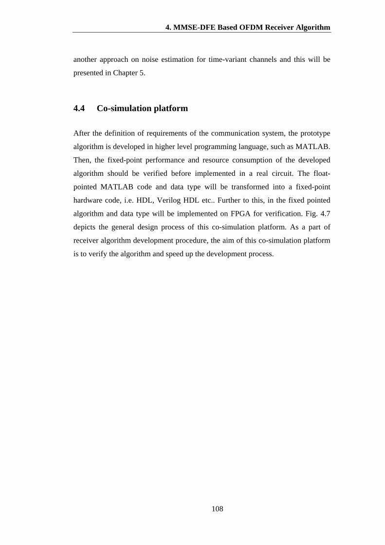
4. MMSE-DFE Based OFDM Receiver Algorithm
108
another approach on noise estimation for time-variant channels and this will be
presented in Chapter 5.
4.4 Co-simulation platform
After the definition of requirements of the communication system, the prototype
algorithm is developed in higher level programming language, such as MATLAB.
Then, the fixed-point performance and resource consumption of the developed
algorithm should be verified before implemented in a real circuit. The float-
pointed MATLAB code and data type will be transformed into a fixed-point
hardware code, i.e. HDL, Verilog HDL etc.. Further to this, in the fixed pointed
algorithm and data type will be implemented on FPGA for verification. Fig. 4.7
depicts the general design process of this co-simulation platform. As a part of
receiver algorithm development procedure, the aim of this co-simulation platform
is to verify the algorithm and speed up the development process.

4. MMSE-DFE Based OFDM Receiver Algorithm
109
Figure 4.7 Algorithm Verification Flow
Co-simulation platforms such as WARP and OPENAIRINTERFACE [105], allow
individual algorithm components to simultaneously run and exchanging
information on FPGAs or DSPs and MATLAB, in a collaborative manner. With
the fixed-point simulation platform, this kind of simulation process can verify
feasibility and evaluate the complexity and performance of a dedicated algorithm.
The existing co-simulation platforms take a considerable amount of time to
convert MATLAB code to HDL code. Besides this, the hardware-software
interface is another important part of the co-simulation system. Because algorithm
modification may require a re-doing of the data interface, which may result in data
interface development being the most time-consuming step during the whole
process system algorithm verification, it is essential to reduce the workload of
interface development. Considering that there already exist some tools which can
automatically transform MATLAB code to HDL code, besides the
implementation of a prototype algorithm, the hardware-software interface is
another important part of the co-simulation system. Considering all the

4. MMSE-DFE Based OFDM Receiver Algorithm
110
substructures of the hybrid estimation algorithm, such as coarse estimation
module, FFT module, CIR estimation module or the DFE module, may be verified
separately, this means different types of data formats will be transmitted via the
interface between the hardware and software. Thus a universal interface that is
capable of various throughput and data widths is required. Therefore, the design
requirements also include high speed, data transmission stability and compatibility
with different data formats for the requirements of different algorithms.
To meet these requirements, a gigabit Ethernet platform is chosen as the interface
between MATLAB and FPGA with the maximum data throughput of 1000 M
bits/sec. Also, in order to achieve maximize throughput, the extended User
Datagram Protocol (UDP) communication protocol is adopted. As described in
Fig. 4.8, the pipeline UDP packet consists of two parts: the payload and header.
The header contains an essential check code for the UDP packet and the payload
part holds the data which is specified in the header.
¢¢¢¢¢¢ ¢¢¢¢¢¢ ¢¢¢¢¢¢
Figure 4.8 UDP Packets Transmission
The hardware part is the crucial part for the verification. It handles not only the
UDP communication between FPGA and PC but also data processing. The
hardware is implemented on a Xilinx ML605 board with Xilinx Virtex6 FPGA.
This co-simulation platform takes advantage of the abundant on-chip resources of
FPGA. The high speed and high performance Digital Clock Management,
dedicated MAC Ethernet IP core, LUTs and embedded high speed DSP 48E1
Slice module work collaboratively provide a high speed universal high speed data
interface and high performance algorithm realization platform. Fig. 4.9 shows the
system diagram of the proposed co-simulation platform. Table 4.1 presents the
entire hardware consumption, which includes consumption of universal data
interface, DFE module, as well as the LTE Turbo decoder. Appendix A and B

4. MMSE-DFE Based OFDM Receiver Algorithm
111
present some other simulation results.
Figure 4.9 System Diagram of Co-simulation Platform
Table 4.1 Hardware Consumption of Some Important FGPA Modules DSP48 Slice
LUTs Block RAM
Hardware Interface 0 959 12 Resampler 30 2274 6
Turbo Decoder 16 29877 69 Overall Hardware resource 769 150720 416
The main contribution of this co-simulation is to propose a universal interface
between MATLAB and FPGA and to provide a flexible verification platform. It
also makes the most of the high speed gigabit Ethernet and the high performance
FPGA.
4.5 Simulation results
In this section, the performance of this hybrid receiver algorithm is evaluated via
computer simulations. As this hybrid algorithm is a combination of classical
algorithm and DFE, the performance of different modules is partly assessed.
Table 4.2 lists the details of the OFDM symbol for the simulation. One burst
format of data that contains 582 data OFDM frames is used in this simulation. In
the simulation, we adjust the CFO and SFO by adding an extra carrier frequency
offset on the input data to simulate CFO in a real situation and using the FPGA

4. MMSE-DFE Based OFDM Receiver Algorithm
112
based resampler to tune the sampling rate of the receiver. Then, the Rayleigh
fading channel is considered, with 9 taps for simulation as described in Table 4.3.
Doppler effect with a different frequency shift is also considered. The channel
process is simulated based on the model in Section2.3.
TABLE 4.2 OFDM Parameters
Parameter Value NSD: number of data subcarriers NSP: number of pilot subcarriers TFFT:FFT and IFFT period TSIGNAL: duration of the signal symbol TCP: CP duration TSYM: symbol interval Sampling rate: Subcarrier Spacing: Modulation Scheme: 16 QAM
TABLE 4.3 Channel Taps in Simulation
Taps Relative delay
(ns)
Fading
(dB) 1 0 -4.6 2 15 -2.0 3 25 -3.0 4 50 0 5 150 -4.3 6 225 -6.5 7 400 -3.0 8 525 -15.2 9 750 -21.7
Fig. 4.10 shows the normalized mean square error (NMSE) curves on the output
of the CFO estimator under different SNR when SFO is 80 ppm. Doppler effects
are not considered in this simulation. The performances of the system under
different CFO are compared. The NMSE of the CFO estimation are obtained from
100 Monte Carlo trials on one SNR value and calculated for 50 OFDM symbols.
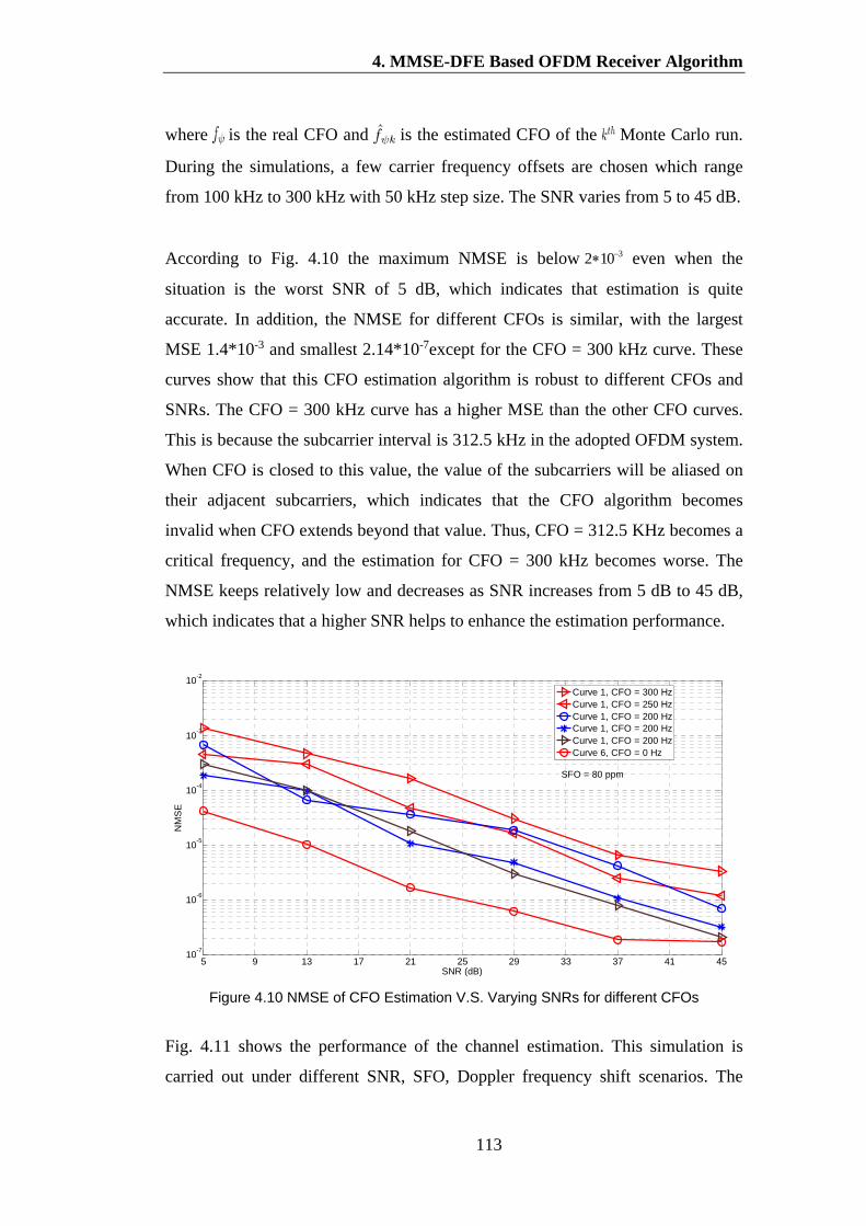
4. MMSE-DFE Based OFDM Receiver Algorithm
113
where is the real CFO and is the estimated CFO of the Monte Carlo run.
During the simulations, a few carrier frequency offsets are chosen which range
from 100 kHz to 300 kHz with 50 kHz step size. The SNR varies from 5 to 45 dB.
According to Fig. 4.10 the maximum NMSE is below 32 10 even when the
situation is the worst SNR of 5 dB, which indicates that estimation is quite
accurate. In addition, the NMSE for different CFOs is similar, with the largest
MSE 1.4*10-3 and smallest 2.14*10-7except for the CFO = 300 kHz curve. These
curves show that this CFO estimation algorithm is robust to different CFOs and
SNRs. The CFO = 300 kHz curve has a higher MSE than the other CFO curves.
This is because the subcarrier interval is 312.5 kHz in the adopted OFDM system.
When CFO is closed to this value, the value of the subcarriers will be aliased on
their adjacent subcarriers, which indicates that the CFO algorithm becomes
invalid when CFO extends beyond that value. Thus, CFO = 312.5 KHz becomes a
critical frequency, and the estimation for CFO = 300 kHz becomes worse. The
NMSE keeps relatively low and decreases as SNR increases from 5 dB to 45 dB,
which indicates that a higher SNR helps to enhance the estimation performance.
Figure 4.10 NMSE of CFO Estimation V.S. Varying SNRs for different CFOs
Fig. 4.11 shows the performance of the channel estimation. This simulation is
carried out under different SNR, SFO, Doppler frequency shift scenarios. The
5 9 13 17 21 25 29 33 37 41 4510
-7
10-6
10-5
10-4
10-3
10-2
SNR (dB)
NM
SE
Curve 1, CFO = 300 HzCurve 1, CFO = 250 HzCurve 1, CFO = 200 HzCurve 1, CFO = 200 HzCurve 1, CFO = 200 HzCurve 6, CFO = 0 Hz
SFO = 80 ppm
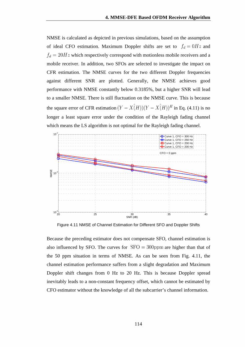
4. MMSE-DFE Based OFDM Receiver Algorithm
114
NMSE is calculated as depicted in previous simulations, based on the assumption
of ideal CFO estimation. Maximum Doppler shifts are set to and
which respectively correspond with motionless mobile receivers and a
mobile receiver. In addition, two SFOs are selected to investigate the impact on
CFR estimation. The NMSE curves for the two different Doppler frequencies
against different SNR are plotted. Generally, the NMSE achieves good
performance with NMSE constantly below 0.3185%, but a higher SNR will lead
to a smaller NMSE. There is still fluctuation on the NMSE curve. This is because
the square error of CFR estimation in Eq. (4.11) is no
longer a least square error under the condition of the Rayleigh fading channel
which means the LS algorithm is not optimal for the Rayleigh fading channel.
Figure 4.11 NMSE of Channel Estimation for Different SFO and Doppler Shifts
Because the preceding estimator does not compensate SFO, channel estimation is
also influenced by SFO. The curves for are higher than that of
the 50 ppm situation in terms of NMSE. As can be seen from Fig. 4.11, the
channel estimation performance suffers from a slight degradation and Maximum
Doppler shift changes from 0 Hz to 20 Hz. This is because Doppler spread
inevitably leads to a non-constant frequency offset, which cannot be estimated by
CFO estimator without the knowledge of all the subcarrier’s channel information.
20 25 30 35 4010
-4
10-3
10-2
SNR (dB)
NM
SE
Curve 1, CFO = 300 HzCurve 1, CFO = 250 HzCurve 1, CFO = 200 HzCurve 1, CFO = 200 Hz
CFO = 0 ppm

4. MMSE-DFE Based OFDM Receiver Algorithm
115
Fig. 4.12 shows the SFO estimation performance for different SFOs and SNRs.
The error vector magnitude (EVM) data is calculated from the output signal of the
SFO estimator, as depicted in Fig. 4.5. As a comparison, the EVM of the received
signal before the SFO estimation is also presented. In this simulation, the CFO is
still set to 0 kHz and SFO = 50 ppm and SFO = 150 ppm are chosen to obtain
brief knowledge of the effects of different SFOs. As a point of reference, the ideal
case with perfect frequency synchronization (SFO = CFO = 0) is also included in
this simulation as Curve 1. As shown in Fig 10, Curve 3 and Curve 5 represent the
EVM performance before SFO estimation, with a minimum EVM of 4% higher
than SFO of estimator processed signal, which shows that SFO has a considerable
impact on signal quality. Besides this, by comparing Curve 2 with Curve 3, and
Curve 4 with Curve 5, we can find that the post-SFO-estimation EVM is reduced
by as much as 13.3% when SNR equals 60 dB, which indicates that the SFO
estimator can largely enhance the EVM performance of received signal. Though
the estimator can significantly improve EVM performance, the residual SFO still
has a marked effect on the EVM curve: the EVM for SFO = 150 ppm is about 0.4%
higher than that of SFO = 50 ppm after the SFO estimation, when SNR is higher
than 30 dB as Curve 2 and 4 depict. The EVM under lower SNR is still high and
requires further compensation.
Figure 4.12 EVM Performance comparisons for SFO Estimator and Preceding Parts
5 10 15 20 25 30 35 400
5
10
15
SNR (dB)
EV
M (
%)
Curve 1, SFO = 0 ppm, After SFO EstimationCurve 2, SFO = 50 ppm, After SFO EstimationCurve 3, SFO = 50 ppm, Before SFO EstimationCurve 4, SFO = 150 ppm, After SFO EstimationCurve 5, SFO = 150 ppm, Before SFO Estimation
CFO = 0 Hz
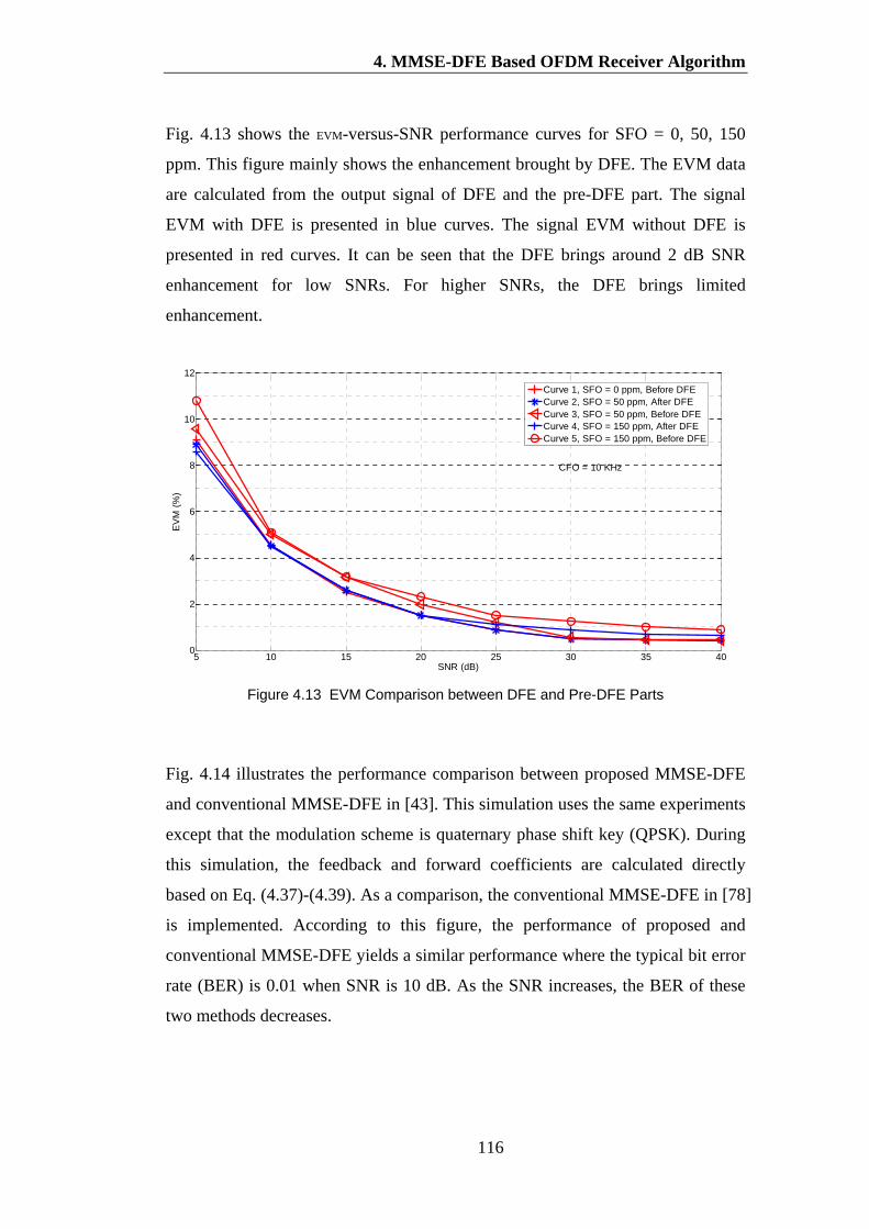
4. MMSE-DFE Based OFDM Receiver Algorithm
116
Fig. 4.13 shows the EVM-versus-SNR performance curves for SFO = 0, 50, 150
ppm. This figure mainly shows the enhancement brought by DFE. The EVM data
are calculated from the output signal of DFE and the pre-DFE part. The signal
EVM with DFE is presented in blue curves. The signal EVM without DFE is
presented in red curves. It can be seen that the DFE brings around 2 dB SNR
enhancement for low SNRs. For higher SNRs, the DFE brings limited
enhancement.
Figure 4.13 EVM Comparison between DFE and Pre-DFE Parts
Fig. 4.14 illustrates the performance comparison between proposed MMSE-DFE
and conventional MMSE-DFE in [43]. This simulation uses the same experiments
except that the modulation scheme is quaternary phase shift key (QPSK). During
this simulation, the feedback and forward coefficients are calculated directly
based on Eq. (4.37)-(4.39). As a comparison, the conventional MMSE-DFE in [78]
is implemented. According to this figure, the performance of proposed and
conventional MMSE-DFE yields a similar performance where the typical bit error
rate (BER) is 0.01 when SNR is 10 dB. As the SNR increases, the BER of these
two methods decreases.
5 10 15 20 25 30 35 400
2
4
6
8
10
12
SNR (dB)
EV
M (
%)
Curve 1, SFO = 0 ppm, Before DFECurve 2, SFO = 50 ppm, After DFECurve 3, SFO = 50 ppm, Before DFECurve 4, SFO = 150 ppm, After DFECurve 5, SFO = 150 ppm, Before DFE
CFO = 10 KHz
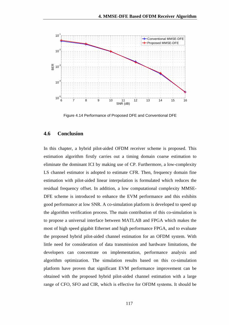
4. MMSE-DFE Based OFDM Receiver Algorithm
117
Figure 4.14 Performance of Proposed DFE and Conventional DFE
4.6 Conclusion
In this chapter, a hybrid pilot-aided OFDM receiver scheme is proposed. This
estimation algorithm firstly carries out a timing domain coarse estimation to
eliminate the dominant ICI by making use of CP. Furthermore, a low-complexity
LS channel estimator is adopted to estimate CFR. Then, frequency domain fine
estimation with pilot-aided linear interpolation is formulated which reduces the
residual frequency offset. In addition, a low computational complexity MMSE-
DFE scheme is introduced to enhance the EVM performance and this exhibits
good performance at low SNR. A co-simulation platform is developed to speed up
the algorithm verification process. The main contribution of this co-simulation is
to propose a universal interface between MATLAB and FPGA which makes the
most of high speed gigabit Ethernet and high performance FPGA, and to evaluate
the proposed hybrid pilot-aided channel estimation for an OFDM system. With
little need for consideration of data transmission and hardware limitations, the
developers can concentrate on implementation, performance analysis and
algorithm optimization. The simulation results based on this co-simulation
platform have proven that significant EVM performance improvement can be
obtained with the proposed hybrid pilot-aided channel estimation with a large
range of CFO, SFO and CIR, which is effective for OFDM systems. It should be
6 7 8 9 10 11 12 13 14 15 1610
-5
10-4
10-3
10-2
10-1
SNR (dB)
BE
R
Conventional MMSE-DFEProposed MMSE-DFE

4. MMSE-DFE Based OFDM Receiver Algorithm
118
noted that there exists some limitations for this receiver: a). The receiver
algorithm copes with the Doppler effect by using MMSE-DFE. However, this
DFE does not make use of features of Doppler effect. Hence, the performance
could be degraded for high mobility scenarios. Further research for high mobility
scenarios could be conducted. The solution could be time domain interpolation or
frequency domain compensation. b). The introducing of MMSE-DFE brings
higher computation complexity with little performance improvement. Hence,
better solution to combat residual impairment could be proposed.
119
5. Subspace-based noise estimation
Signal-to-noise ratio (SNR) estimation is an important algorithm for in receivers.
It provides prior knowledge for channel equalization, as described in Chapter 4. In
addition, it also plays an important role in adaptive modulation in LTE system.
Based on the knowledge that the received signal space consists of signal subspace
and noise subspace, this chapter proposes a subspace-based SNR estimation
solution to cope with the time-varying channel, with frequency selective effect
and different OFDM pilot structure situations for LTE.
5.1 Introduction
The LTE adopts OFDM modulation for downlink transmission. At the receiver
side, several techniques have been proposed to improve the received ODFM
signal quality, including LMMSE channel estimation [117], and the previously
proposed MMSE-DFE. These techniques are based on accurate Signal-to-Noise
Ratio (SNR) estimation in the frequency selective fading channel. In addition,
adaptive modulation and coding (AMC) are utilized to achieve high throughput in
various channel conditions. The code rate and modulation scheme is adaptively
changed according to the channel quality, which requires accurate SNR estimation.
Hence, accurate SNR estimation is essential for receiver algorithm design.
A variety of SNR estimation methods have been investigated [45-47, 118, 119].
[118] makes use of a data-aided and decision-directed algorithm to cope with the
SNR estimation problem in DVB-RCS systems. [45] utilizes zero point auto-
correlation of the received signal to estimate SNR based on the assumption that
the channel is constant throughout the observation period, which is not valid in
practice. A few papers have investigated SNR estimation in the time variant
5. Subspace-based Noise Estimation
120
channel. In [46, 118], the Data-Aided (DA) maximum likelihood (ML) estimator
is presented. [47] proposes a subspace-based method for an OFDM system. These
algorithms give good SNR estimation performance in time-varying channel.
However, they are not fully compatible with the pilot structures in LTE system. In
3GPP specification, the resource is allocated in the form of resource block (RB) in
which different numbers and locations of subcarriers are allocated. The
requirements for SNR estimation include:
1) The estimator can work with different pilot patterns, where the pilot
number can be large or very small.
2) The estimator can cope with the time-varying channel.
In this chapter, a subspace based SNR estimator is introduced which can work
with varieties of pilot patterns in a time varying channel. The advantage of this
method is that the SNR can be obtained accurately in different conditions
regarding pilot patterns. The chapter is organized as follows. In Section 5.2, the
system model for this estimation algorithm is described. Section 5.3 presents this
subspace-based SNR estimation algorithm. In Section 5.4, the simulation results
and comparisons are presented. Finally, the conclusions are drawn in Section 5.5.
5.2 System model
5.2.1 Applicable pilot scenarios
LTE adopts an OFDMA scheme in which the radio resource is allocated to each
user dynamically in terms of RB. Though the base station broadcasts the same
reference signal pattern to all users, different users may share different radio
resources. Hence, the pilot pattern within the accessible radio resource for each
user is flexible. In addition, LTE also adopts AMC, in which the pilot pattern
could be dynamically generated by the base station according to the subcarrier
spacing, RB allocation, cyclic prefix type and slot number.
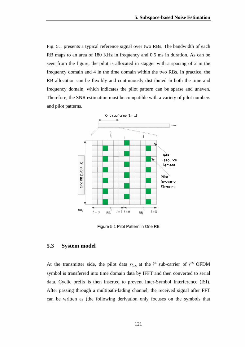
5. Subspace-based Noise Estimation
121
Fig. 5.1 presents a typical reference signal over two RBs. The bandwidth of each
RB maps to an area of 180 KHz in frequency and 0.5 ms in duration. As can be
seen from the figure, the pilot is allocated in stagger with a spacing of 2 in the
frequency domain and 4 in the time domain within the two RBs. In practice, the
RB allocation can be flexibly and continuously distributed in both the time and
frequency domain, which indicates the pilot pattern can be sparse and uneven.
Therefore, the SNR estimation must be compatible with a variety of pilot numbers
and pilot patterns.
0l0RB 5l 0l 5l 0RB
1RB
Figure 5.1 Pilot Pattern in One RB
5.3 System model
At the transmitter side, the pilot data at the sub-carrier of OFDM
symbol is transferred into time domain data by IFFT and then converted to serial
data. Cyclic prefix is then inserted to prevent Inter-Symbol Interference (ISI).
After passing through a multipath-fading channel, the received signal after FFT
can be written as (the following derivation only focuses on the symbols that

5. Subspace-based Noise Estimation
122
contain pilots. Hence, in the formula refers to the symbol that contains a
pilot):
(5.1)
where represents the channel frequency response at the subcarrier of
OFDM symbol; and represents the AWGN noise with variance
. The de-patterned signal can be expressed as:
(5.2)
Assuming , the noise power will not be changed by the de-patterning
process. Therefore, the SNR of the received signal depends on the channel and
noise power. The average SNR in this dissertation is defined as:
(5.3)
The SNR estimation task can be decomposed into a signal power estimation
problem to estimate the average channel power in the presence of
noise; and a noise power estimation problem to estimate variance in the
presence of a time varying channel.
5.3.1 Conventional moving average method
The most common SNR estimation method is to use the moving average filter to
filter out AWGN noise from the signal, which is adopted in WCDMA and 802.11
a/g/n systems [120, 121]. This method provides a good estimate of noise variance
by averaging operations. It can also be transplanted to LTE system. The SNR
estimation can be realized subcarrier-by-subcarrier.

5. Subspace-based Noise Estimation
123
¡
+
Figure 5.2 Moving Average Based SNR Estimation
Fig. 5.2 shows the SNR estimation method based on the moving average filter.
Firstly, the de-patterned pilots at the subcarrier are moving averaged over
OFDM symbols, as shown at Point B in Fig. 5.2. Under the assumption that the
mean of noise is 0, the noise effect is removed from the signal component through
the averaging operation. After that, the signal power is estimated by calculating
the square of the signal as shown at Point D. The estimation of the signal power
can be expressed as:
(5.4)
Secondly, the noise component can be estimated by subtracting the signal
estimates from the de-patterned pilots, as shown at Point A. The instantaneous
noise power (square of each noise sample) is averaged to estimate the mean noise
power at Point C. The estimate of the noise power can be written as:
(5.5)
The moving average based SNR estimation gives good performance in AWGN
channels. The larger value gives a more accurate estimate of the signal
component, which will in turn give a more accurate estimate of the noise
component. However in time varying channels, the value of should be smaller
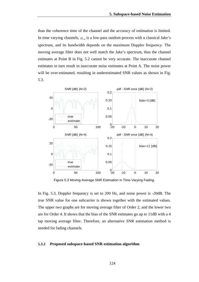
5. Subspace-based Noise Estimation
124
than the coherence time of the channel and the accuracy of estimation is limited.
In time varying channels, is a low-pass random process with a classical Jake’s
spectrum, and its bandwidth depends on the maximum Doppler frequency. The
moving average filter does not well match the Jake’s spectrum, thus the channel
estimates at Point B in Fig. 5.2 cannot be very accurate. The inaccurate channel
estimates in turn result in inaccurate noise estimates at Point A. The noise power
will be over-estimated, resulting in underestimated SNR values as shown in Fig.
5.3.
Figure 5.3 Moving Average SNR Estimation in Time Varying Fading.
In Fig. 5.3, Doppler frequency is set to 200 Hz, and noise power is -20dB. The
true SNR value for one subcarrier is shown together with the estimated values.
The upper two graphs are for moving average filter of Order 2, and the lower two
are for Order 4. It shows that the bias of the SNR estimates go up to 11dB with a 4
tap moving average filter. Therefore, an alternative SNR estimation method is
needed for fading channels.
5.3.2 Proposed subspace-based SNR estimation algorithm
0 50 100
-20
0
20
SNR [dB] (N=2)
true
estimate
0 50 100
-20
0
20
SNR [dB] (N=4)
true
estimate
-20 -10 0 10 200
0.05
0.1
0.15
0.2pdf - SNR error [dB] (N=2)
bias=3 [dB]
-20 -10 0 10 200
0.05
0.1
0.15
0.2pdf - SNR error [dB] (N=4)
bias=11 [dB]

5. Subspace-based Noise Estimation
125
Signal-spacing theorem is one of the foundations of signal processing [122]. The
basic idea is to view the signal as vectors in a certain signal space, which is
spanned by a set of bases. In [47], the noise power is estimated by means of
decomposing the received pilot signals into a signal-space and noise space. This
approach gives good performance when pilot numbers are large and assumes the
pilots are evenly inserted into every OFDM symbol, whereas the number and
pattern of pilots are uncertain in the LTE case. In this method, we focus on
investigating the subspace based SNR estimation when pilot patterns and numbers
are flexible. Fig. 5.4 shows the proposed SNR estimation procedure.
FFT De-pattern
++¡
CBA
Figure 5.4 Proposed SNR estimation process
In the multipath channel, the de-patterned signal in Eq. (5.2) can be rewritten as
(5.6)
where is the complex channel gain of the path at pilot-contained
OFDM symbol; is the time delay of path in terms of sample points.
Considering an observation time , a group of pilots are received. Among them,
pilots are selected as observation vector, for example:
, where is time index and is the pilot in
time index. For example, the pilot at subcarrier in Resource Block
0 and the pilot subcarriers in Resource Block 1 are chosen as the
observation vector: . Eq. (5.6) can be rewritten in
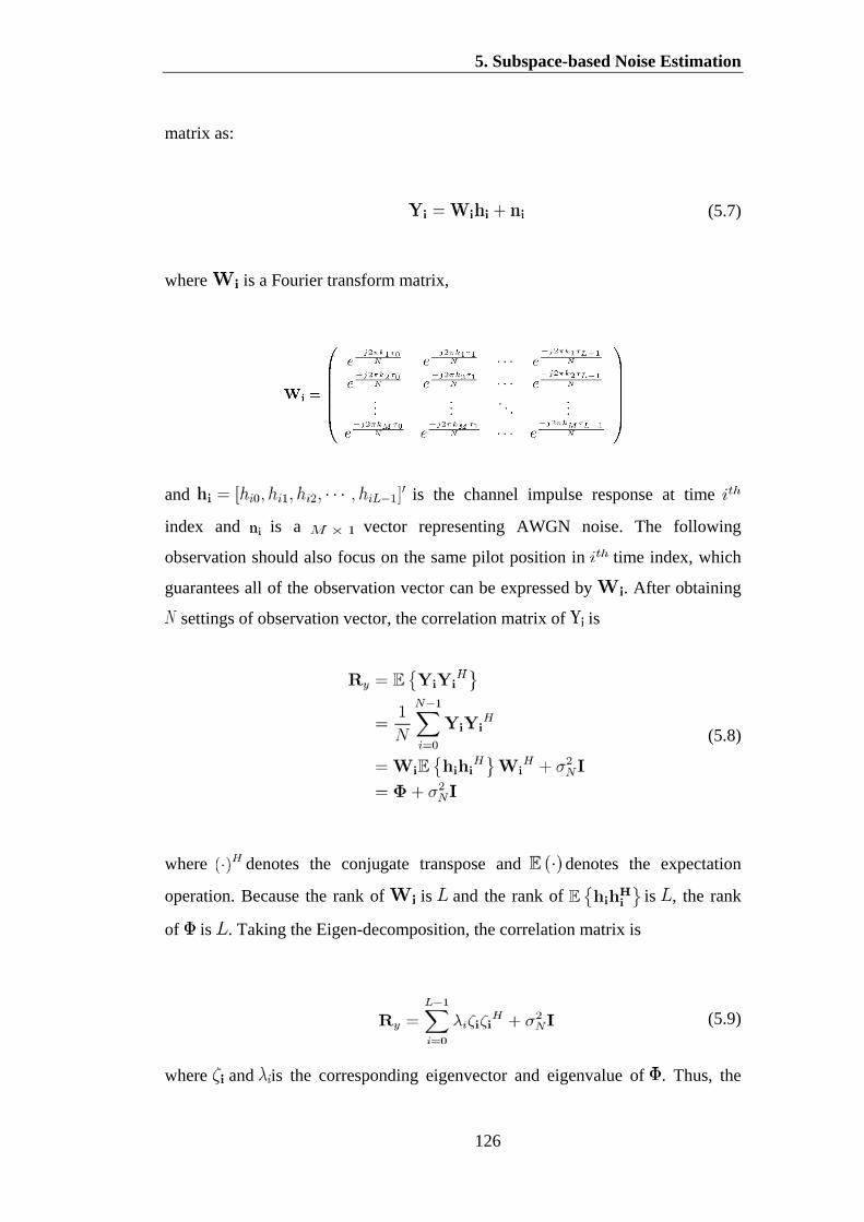
5. Subspace-based Noise Estimation
126
matrix as:
(5.7)
where is a Fourier transform matrix,
and is the channel impulse response at time
index and is a vector representing AWGN noise. The following
observation should also focus on the same pilot position in time index, which
guarantees all of the observation vector can be expressed by . After obtaining
settings of observation vector, the correlation matrix of is
(5.8)
where denotes the conjugate transpose and denotes the expectation
operation. Because the rank of is and the rank of is , the rank
of is . Taking the Eigen-decomposition, the correlation matrix is
(5.9)
where and is the corresponding eigenvector and eigenvalue of . Thus, the
5. Subspace-based Noise Estimation
127
observation signal can be viewed as consisting of a signal space spanned by an L
dimension basis and an M dimension noise space. Assuming the eigenvalue of
is , the smallest eigenvalues theoretically
equal to . In practice, the difference between these eigenvalues can be very
large. The noise power can only be estimated from these eigenvalues by:
(5.10)
According to Eq. (5.10), is essential to compute the noise variance. can be
estimated by the Minimum Description Length (MDL) criterion presented in
[123]. The MDL method was firstly applied to super-resolve the number of
ssignal sources [123]. Further to this, this algorithm is applied to search the
multipath channel components where the weak components can be ignored [124].
This criterion constructs the objective function:
(5.11)
Then, the can be obtained by minimizing this objective function:
(5.12)
When the channel cannot be estimated accurately under severe noise conditions,
the channel power approximately equals to:

5. Subspace-based Noise Estimation
128
(5.13)
Then the SNR can be calculated as.
where and are obtained from Eq. (5.10) and (5.13), respectively.
Modified MDL method
The classical MDL criterion in [123] estimates the path without regarding the
power of each path which may lead to an overestimation ( ) in small pilot
number situations. Table 5.1 demonstrates this phenomenon. The 16 pilots LTE
signal is transmitted in the EVA-5 Hz channel [125], which has a channel length
of 9. It can be seen that the estimated number of path that minimizes the MDL
criterion is 15, which corresponds to , whereas the optimum number of
path that minimizes the SNR normalized mean square error (NMSE) is 2, which
corresponds to .
Table 5.1 Estimation Results of MDL Method 0 1 2 3 4 5
319.5086 92.3797 52.4506 42.4244 29.3170 25.5680
3269.1 2834.9 2632.4 2432.0 2317.1 2177.6
SNR
NMSE 2.45
0.4485
(Minimum
SNR
NMSE)
3.9095 10.4341 17.5976 27.6895
6 7 8 9 10 11
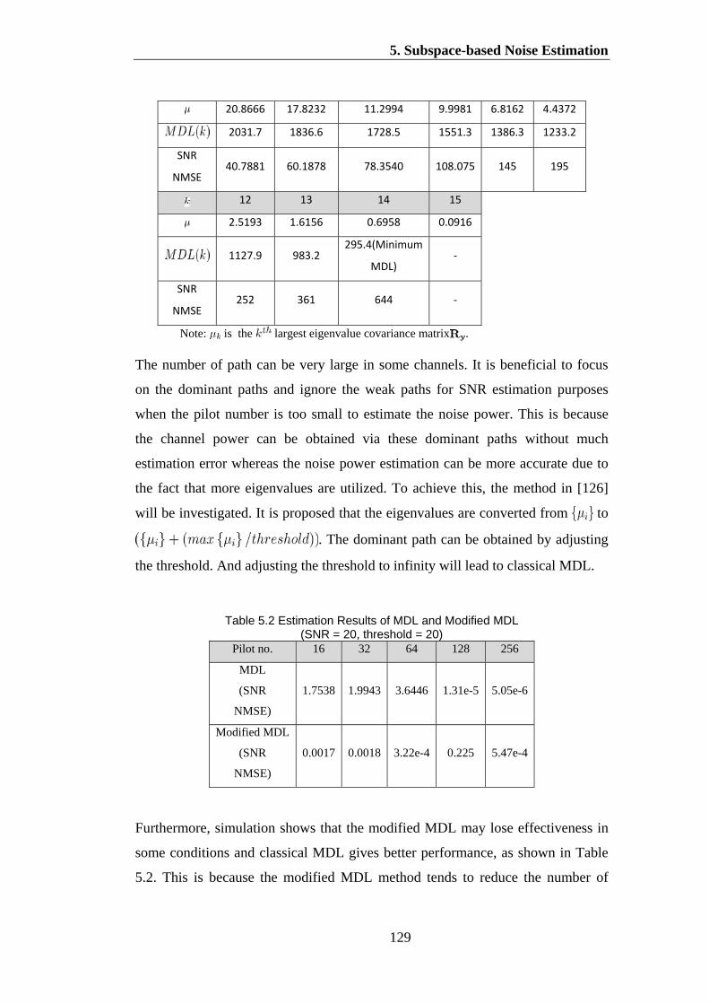
5. Subspace-based Noise Estimation
129
20.8666 17.8232 11.2994 9.9981 6.8162 4.4372
2031.7 1836.6 1728.5 1551.3 1386.3 1233.2
SNR
NMSE 40.7881 60.1878 78.3540 108.075 145 195
12 13 14 15
2.5193 1.6156 0.6958 0.0916
1127.9 983.2 295.4(Minimum
MDL) -
SNR
NMSE 252 361 644 -
Note: is the largest eigenvalue covariance matrix .
The number of path can be very large in some channels. It is beneficial to focus
on the dominant paths and ignore the weak paths for SNR estimation purposes
when the pilot number is too small to estimate the noise power. This is because
the channel power can be obtained via these dominant paths without much
estimation error whereas the noise power estimation can be more accurate due to
the fact that more eigenvalues are utilized. To achieve this, the method in [126]
will be investigated. It is proposed that the eigenvalues are converted from to
. The dominant path can be obtained by adjusting
the threshold. And adjusting the threshold to infinity will lead to classical MDL.
Table 5.2 Estimation Results of MDL and Modified MDL (SNR = 20, threshold = 20)
Pilot no. 16 32 64 128 256
MDL
(SNR
NMSE)
1.7538 1.9943 3.6446 1.31e-5 5.05e-6
Modified MDL
(SNR
NMSE)
0.0017 0.0018 3.22e-4 0.225 5.47e-4
Furthermore, simulation shows that the modified MDL may lose effectiveness in
some conditions and classical MDL gives better performance, as shown in Table
5.2. This is because the modified MDL method tends to reduce the number of

5. Subspace-based Noise Estimation
130
“channel eigenvalues” and increase the number of “noise eigenvalues”. In
addition, the classical MDL method can achieve an accurate channel length
estimation in large pilot number situations. The power estimation of channel and
noise will be accurate due to the accurate channel length estimation and utilization
of large numbers of eigenvalues. In this situation, a flexible use of classical MDL
method is proposed by adjusting the threshold and making a selection between
conventional and modified MDL, according to the results in Table 5.2. The whole
estimation procedure will be summarized in Fig. 5.5:
Figure 5.5 Proposed Subspace-based SNR Estimation
5.4 Simulation results
The algorithm performance is verified in both a PC and laboratory environment.
The MATLAB based simulation platform provides the LTE downlink physical
layer protocol in which the reference signal and user RBs can be configured
flexibly. The laboratory environment consists of a fading channel emulator and
Aeroflex PXI modules. The fading channel emulator can provide a real time Over-
the-Air (OTA) wireless fading channel environment. The PXI modules in the
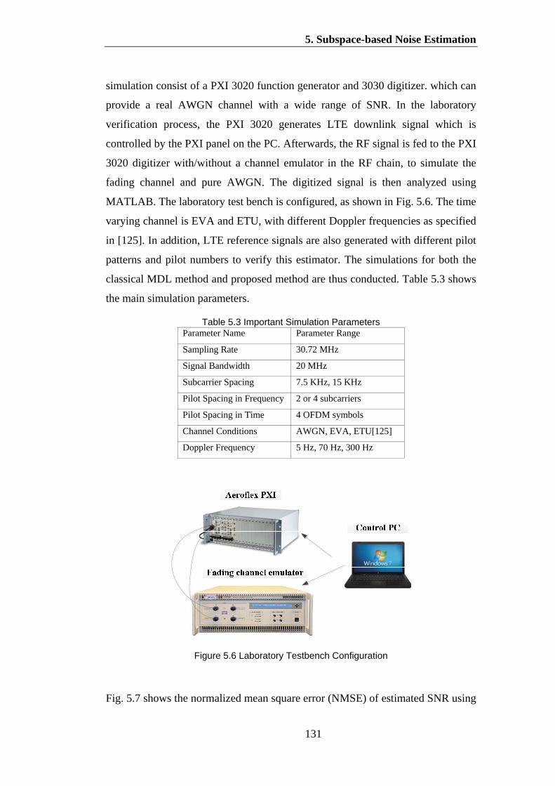
5. Subspace-based Noise Estimation
131
simulation consist of a PXI 3020 function generator and 3030 digitizer. which can
provide a real AWGN channel with a wide range of SNR. In the laboratory
verification process, the PXI 3020 generates LTE downlink signal which is
controlled by the PXI panel on the PC. Afterwards, the RF signal is fed to the PXI
3020 digitizer with/without a channel emulator in the RF chain, to simulate the
fading channel and pure AWGN. The digitized signal is then analyzed using
MATLAB. The laboratory test bench is configured, as shown in Fig. 5.6. The time
varying channel is EVA and ETU, with different Doppler frequencies as specified
in [125]. In addition, LTE reference signals are also generated with different pilot
patterns and pilot numbers to verify this estimator. The simulations for both the
classical MDL method and proposed method are thus conducted. Table 5.3 shows
the main simulation parameters.
Table 5.3 Important Simulation Parameters Parameter Name Parameter Range
Sampling Rate 30.72 MHz
Signal Bandwidth 20 MHz
Subcarrier Spacing 7.5 KHz, 15 KHz
Pilot Spacing in Frequency 2 or 4 subcarriers
Pilot Spacing in Time 4 OFDM symbols
Channel Conditions AWGN, EVA, ETU[125]
Doppler Frequency 5 Hz, 70 Hz, 300 Hz
Figure 5.6 Laboratory Testbench Configuration
Fig. 5.7 shows the normalized mean square error (NMSE) of estimated SNR using

5. Subspace-based Noise Estimation
132
the proposed method in the EVA and ETU channels, with 5 Hz and 70 Hz
Doppler frequencies. This simulation is conducted in MATLAB, which utilizes an
LTE signal consisting of 256 pilot subcarriers and 256 data subcarriers. These
pilot subcarriers and data subcarriers are uniformly distributed in 22 RBs, with
subcarrier spacing of . It is demonstrated that the estimation gives the
worst error of 1% NMSE at SNR of 2 dB in different fading channels. For higher
SNR scenarios, the proposed estimation method yields good performance.
Figure 5.7 SNR NMSE v.s. SNR for Different Channels
The simulation is also carried out using Aeroflex PXI modules. The PXI 3020 is
an arbitrary waveform generator which can operate from 100 MHz to 6 GHz. The
20 MHz bandwidth reference signal is first generated on MATLAB with the
baseband signal filtered via the EVA-300 Hz channel. In order to emulate the
downlink transmission in the AGWN channel, the deteriorated signal is then fed
into the PXI 3030 directly. The RF signal power is tuned to simulate different
SNR scenarios. The RF output is then captured by the PXI 3030 digitizer and
analyzed in MATLAB. Fig. 5.8 shows the estimation performance. It can be
shown that the proposed algorithm yields a maximum error of 9% at 5 dB SNR
when 16 pilots are used. As actual SNR increases, the estimation results become
more accurate. The results are reliable when actual SNR is higher than 20 dB.
Another finding is that the estimation is more accurate when larger numbers of
pilots are used. This is because larger numbers result in a higher dimension
correlation matrix. Hence more eigenvalues are averaged to estimate the SNR. It
0 1 2 3 4 5 6 7 8 9 10 11 12 13 14 15 16 17 18 19 20 21 22 23 24 25 26 27 28 29 300
0.001
0.002
0.003
0.004
0.005
0.006
0.007
0.008
0.009
0.01
SNR
SN
R N
MS
E
Simulation Results for SNR NMSE over Varying SNR under Different Channel
EVA-5Hz, Matlab SimulationEVA-70Hz, Matlab SimulationETU-5Hz, Matlab SimulationETU-70Hz, Matlab Simulation

5. Subspace-based Noise Estimation
133
can also be seen that the estimation results of 16 and 32 pilots achieve accurate
estimation performance, which verifies the modified MDL method.
Figure 5.8 SNR Estimation Result with Different Pilot in PXI Modules
The estimation performance in the fading channel is verified with the help of the
fading channel emulator, as shown in Fig. 5.6. In this emulation, the PXI 3020
generates a 20MHz bandwidth RF signal. Then, the RF signal passes through the
channel emulator. Afterwards, the deteriorated signal is captured by the PXI 3030.
The pilot that are distributed in the whole bandwidth and modified MDL is
adopted, which means only the MDL method is used to estimate the channel
components. Fig. 5.9 shows the estimation results. It can be seen that the proposed
SNR estimation achieved accurate results with minimum SNR estimation error.
5 6 7 8 9 10 11 12 13 14 15 16 17 18 19 20 21 22 23 24 25 26 27 28 29 300
0.01
0.02
0.03
0.04
0.05
0.06
0.07
0.08
0.09
SNR
SN
R N
MS
E
EVA-300; 16 pilots
EVA-300; 32 pilots
EVA-300; 64 pilots
EVA-300; 128 pilots
5. Subspace-based Noise Estimation
134
Figure 5.9 Emulation Results for Subspace-based Noise Variance Estimation
Fig. 5.10 compares the performance of different estimation methods under an
EVA-5 Hz channel in a MATLAB simulation. The conventional moving average
filter method is also simulated, as shown in green curves. In this simulation, we
adopted 3 different numbers of pilots, namely, 16, 64 and 256. This configuration
of number of pilots aims to verify the robustness of the 3 algorithms when
different pilot pattern are used. The performance of classical MDL method is
shown in red curves. The performance of proposed method is shown in blue
curves. It can be seen that the classical MDL method gives large bias when
numbers of pilot is small. According to the green curves, the moving average
method gives biased results when SNR is high, The proposed method keeps good
linearity for small numbers of pilots over the whole SNR range. For larger
numbers of pilots, namely 256, the proposed method gives 9 dB estimation error,
which indicates that it is better to use less numbers of pilot.
5 10 15 205
10
15
20
Actual SNR
Mea
sure
d S
NR
eva5
etu5ideal

5. Subspace-based Noise Estimation
135
Figure 5.10 Comparison of Different SNR Estimation Methods
5.5 Conclusion
This chapter presents an SNR estimation approach that is suitable for the different
pilot patterns and numbers in LTE systems. This approach is based on sub-space
decomposition. Unlike the conventional moving average based SNR estimation
methods, this estimator utilizes distributed pilots in different RBs and adaptively
adjusts the estimation method according to the pilot numbers. Simulation on PC
and Aeroflex PXI modules shows the estimator gives an accurate SNR estimation
performance in a time varying channel. However, there exists some estimation
error when larger numbers of pilot is used for estimation for SNRs. It is
recommended that less numbers of pilot to be used. This approach can be
implemented in the other services in LTE, TD-LTS, LTE-Advanced systems,
where pilots data are adopted. As the complexity of eigen-decomposition is
relatively high when is large, future study will focus on reducing the complexity
by methods such as eigenvalues tracking, or smallest eigenvalue evaluation.
5 7 9 11 13 15 17 19 21 23 25 27 29 300
10
20
30
40
50
60
70
80
SNR (dB)
Est
imat
ed S
NR
16 Pilots, Classibel MDL64 Pilots, Classibel MDL256 Pilots, Classibel MDL16 Pilots, Proposed MDL64 Pilots, Proposed MDL256 Pilots, Proposed MDL16 Pilots, Moving average64 Pilots, Moving average256 Pilots, Moving average

161
6. Robust CRS interference cancellation
Heterogeneous networks are introduced in LTE Release 10+ to improve the link
performance. The architecture introduces co-existence of Macro and Pico cell
which can alleviate the potential traffic congestion caused by increased user
density. Along with the co-existence of different cells comes the disadvantage of
inter-cell interference. Although almost blank subframe (ABS) is proposed to
mitigate the interference, the reference signal in ABS still inevitably causes
interference. This chapter focuses on the interference cancellation by utilizing the
information in the ABS. First, the interfering signal model which takes account of
the channel effect, time and frequency error is presented. Based on this model, an
interference cancellation scheme is studied. The timing and carrier frequency
offset of the interfering signal is compensated. Afterwards, the reference signal of
interfering cell is generated locally and channel response is estimated by making
use of channel statistics. Then, the interfering signal is reconstructed based on the
previous estimate of channel, timing and carrier frequency offset. The interference
is then mitigated by subtracting the estimate of interference signal and LLR
puncturing. Computer simulation results show that the proposed interference
cancellation algorithm significantly improves the performance in different channel
conditions.
6.1 Introduction
Heterogeneous network (HetNet) with macro and pico cell is introduced to meet
the huge traffic demand and to extend the coverage. In this network topology, the
high power (1~40 W) macro cell provides basic coverage and the low power (250
mW) pico cell serves as a complementary cell. The pico cell can functionally
extend network coverage and off-load data traffic of macro-cell, which reduces
6. Robust CRS Interference Cancellation
137
cost and increase frequency efficiency. It provides flexibility for end users to
deploy pico cells by themselves. In such a case, only closed UE group (CSG) UE
can access the pico cell while non-CSG UEs are not allowed to access eve they
are within the coverage of a pico cell. Hence, the not CSG will suffer interference
from pico cell. Apart from this, the UEs served by pico cell will also receive RF
signal from neighboring high power macro cells. Thus, the end users suffer not
only signal decay but also severe interference transmissions of neighboring cells.
This is a common problem when the pico cell works to off-load the data traffic of
neighboring macro cells. This issue is even servere when users of the pico cell
stay within the coverage of macro cells with range extension enabled [127].
In Release 10, Enhanced inter-cell interference coordination (eICIC) is introduced
to address this issue. eICIC proposes two techniques. First, the signal strength is
biased to pico-cell which reduces the interference power. However, this is not
realistic because the broadcast users cannot provide the essential channel
information to the network when it adopts unidirectional link. Second, macro cell
remains silent for certain periods, termed almost blank subframe (ABS) [128].
During the ABS, the physical downlink shared channel (PDSCH) is empty [127].
Hence, UE will not receive PDSCH during ABS period and the inter-cell
interference can be alleviated. However, the users can still receive cell specific
reference signal (CRS), paging channel (PCH), physical broadcast channel
(PBCH), and synchronization channels (PSS/SSS) which degrades the
performance. Hence, the further eICIC (FeICIC) is proposed in Release 11 to
eliminate this CRS interference problem.
The neighbor cell (NC) CRS interference can be divided into colliding and non-
colliding scenarios. In colliding CRS scenario, the NC CRS overlap the serving
cell (SC) CRS. In non-colliding CRS scenario, the NC CRS interferes the
data/control REs. A few researches on CRS interference mitigation were
conducted. In [52, 53], Hard/soft log-likelihood radio (LLR) puncturing method is
proposed for non-colliding CRS scenario. The direct CRS interference
cancellation is studied in [54, 55], where the colliding interfering CRS channel is
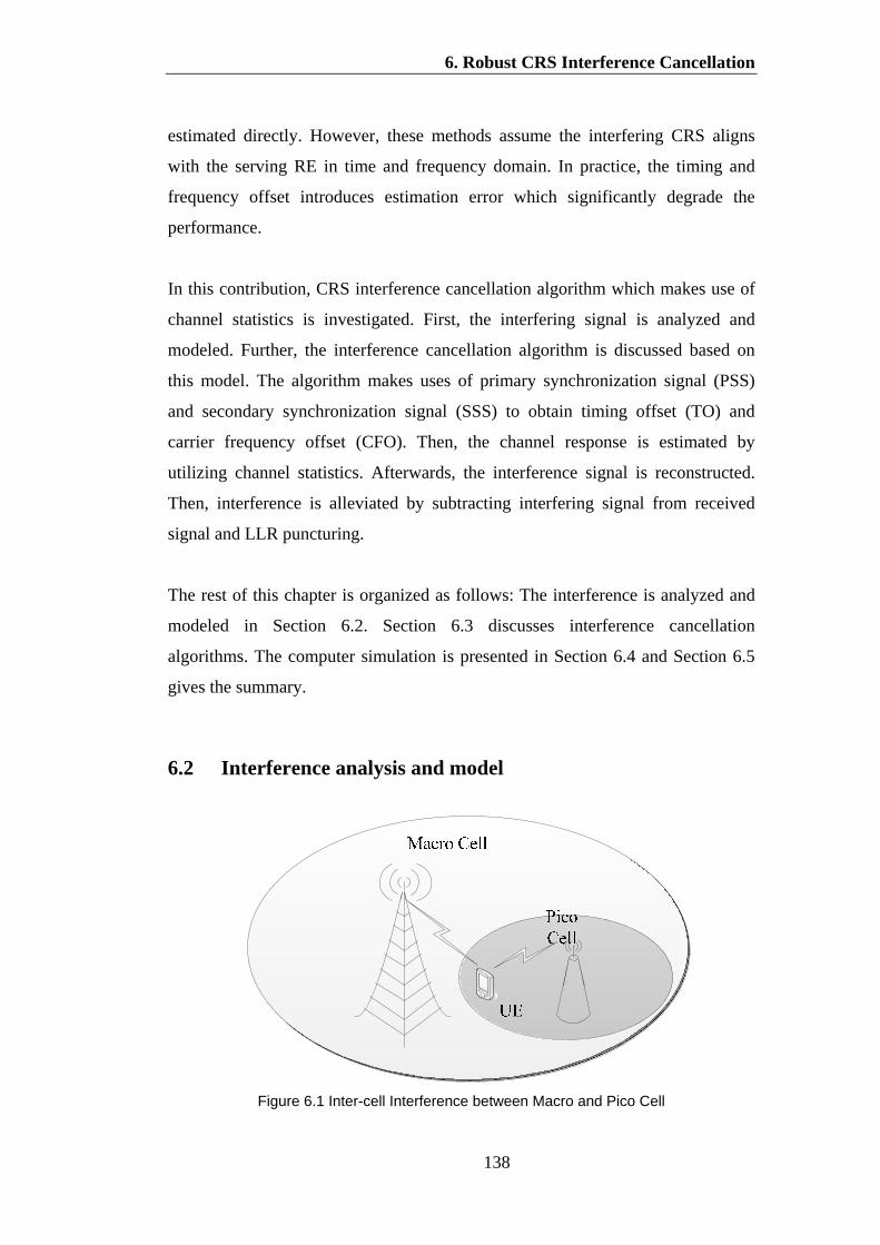
6. Robust CRS Interference Cancellation
138
estimated directly. However, these methods assume the interfering CRS aligns
with the serving RE in time and frequency domain. In practice, the timing and
frequency offset introduces estimation error which significantly degrade the
performance.
In this contribution, CRS interference cancellation algorithm which makes use of
channel statistics is investigated. First, the interfering signal is analyzed and
modeled. Further, the interference cancellation algorithm is discussed based on
this model. The algorithm makes uses of primary synchronization signal (PSS)
and secondary synchronization signal (SSS) to obtain timing offset (TO) and
carrier frequency offset (CFO). Then, the channel response is estimated by
utilizing channel statistics. Afterwards, the interference signal is reconstructed.
Then, interference is alleviated by subtracting interfering signal from received
signal and LLR puncturing.
The rest of this chapter is organized as follows: The interference is analyzed and
modeled in Section 6.2. Section 6.3 discusses interference cancellation
algorithms. The computer simulation is presented in Section 6.4 and Section 6.5
gives the summary.
6.2 Interference analysis and model
Figure 6.1 Inter-cell Interference between Macro and Pico Cell

6. Robust CRS Interference Cancellation
139
Fig. 6.1 is an illustration of typical inter-cell interference scenario between macro
and pico cells, in which the LTE service is delivered to the UE via pico cell and
the downlink signal from macro cell interferes the UE at the edge of pico cell. To
alleviate the inter-cell interference, the ABS is transmitted by the macro cell,
during which only certain control signals are transmitted, such as CRS. However,
the CRS still cause interference to the UE. Fig. 6.2 shows the received signal of
one resource block (RB) with one interference cell. As shown in this figure, the
CRS signal from neighboring macro cell overlaps the data resource elements
(REs) in the time and frequency grid. Due to the STO and CFO between the
interfering cell and UE, the received interfering signal suffers STO and CFO as
shown in Fig. 6.2.
i = 0
Figure 6.2 Received signal in time and frequency grid
The LTE downlink transmission employs OFDM modulation, in which the
frequency domain signal of OFDM symbol is transferred to time domain
signal via N-point Fast Fourier Transform (FFT):
6. Robust CRS Interference Cancellation
140
(6.1)
where and represent the data and pilot respectively.
Then the signal is transmitted over a multipath propagation channel take into
account the additive white Gaussian noise (AWGN). At the receiver side, the
received signal can be written as:
(6.2)
where and are the gain and the delay of the path, respectively; and is
the AWGN. Due to the STO and CFO, the corrupted signal in the case of inter-
cell interference is:
(6.3)
where and are the serving and interfering signal respectively;
and are the frequency response of the serving and interfering channel; and
is the relative timing and frequency offset between the interfering and UE cell.
After applying the N-point FFT, the OFDM symbol is given by [36]:

6. Robust CRS Interference Cancellation
141
(6.4)
where and denote the channel coefficients of serving and interfering cell
at subcarrier respectively; stands for the inter-carrier interference (ICI).
During the ABS, only certain control signal is transmitted and the CRS signal
from interfering cell overlaps the data REs of serving cell as shown in Fig. 6.2.
The signal model at the data RE of the serving cell with interference can be
written as:
(6.5)
According to Eq. (6.5), the relative timing offset between interfering and serving
cell causes phase shift on subcarrier. The terms in Eq. (6.5) arises from
CFO term , which results in inter-carrier interference (ICI). This model shows
single-input single-output (SISO) antenna case only. The multiple-input multiple-
output (MIMO) antenna case can be easily derived based on Eq. (6.5). However,
the number of RE will increase since the number of interference CRS increases
with number of antenna ports, which results in more severe interference. These
problems will be addressed in Section 6.3.
6.3 Interference cancellation algorithm

6. Robust CRS Interference Cancellation
142
Yi ;k
Figure 6.3 CRS Interference Cancellation Receiver Architecture
The proposed cancellation algorithm is shown in Fig. 6.3. Based on the
conventional LTE receiver modules, this algorithm intoduces the following parts:
TO/CFO estimation, interfering channel estimation, interfering cell modeling and
interfering signal reconstruction and reduction. In CFO/TO estimation, the
relative frequency offset and timing offset between the interfering cell and serving
cell is estimated by using PSS/SSS generated in interfering cell modeling. Next,
the interfering channel estimation is conducted based on the compensated signal.
The interfering signal is then reconstructed based on the previous estimation and
subtracted from the received signal. Finally, due to the inaccurate estimation of
SNR, the log-likelihood ratio (LLR) is scaled to adjust the SNR mismatch.
6.3.1 TO/CFO estimation
The objective of this module is to retrieve interfering OFDM symbol timing and
estimate the CFO of the interfering cell. Many timing and frequency
synchronization algorithms have been developed. Most of them exploit the
periodic nature of the time-domain signal by using cyclic prefix (CP) [129-131] or
pilot data [132, 133]. However, the data REs are zero in ABS, which significantly
reduces the power of CP. The low SNR of CP makes it difficult for both timing
and frequency synchronization. However, thePSS and SSS can be used. The PSS
and SSS are at the last and second-last symbol in the time slot 0 and slot 10 as
shown in Fig. 6.4. The PSS and SSS in frequency domain is given
by:

6. Robust CRS Interference Cancellation
143
And
where is 25, 29 or 34 corresponding to the physical layer identity ; and
are derived from the physical layer cell identity group . Because the entire
PSS/SSS symbol only contains PSS/SSS signal, which means the PSS/SSS
symbol could be used for synchronization. As the time domain PSS/SSS symbol
can make full use of CP and gives better performance, this paper adopts time
domain synchronization method. The timing and frequency offset can be
estimated by utilizing the cross-correlation of PSS/SSS [131]:
(6.6)
where
(6.7)
and is the received signal with a delay of .
and and are the received and locally generated symbols which contain
PSS/SSS. Note that the generation of PSS/SSS is based on the assumption of ideal
cell search. The cell search algorithm in inter-cell interference scenario is beyond
of the scope of this dissertation. After the timing and frequency synchronization
of the interfering signal, the interfering channel response can be estimated.

6. Robust CRS Interference Cancellation
144
¢¢¢¢¢¢ ¢¢¢¢¢¢
Figure 6.4 Synchronization Signal
6.3.2 Interfering channel estimation
Before interference cancellation, it’s essential to estimate the NC CRS channel
response. Based on the estimation of Eq. (6.6), the relative position of NC CRS on
time-frequency grid is determined. When the NC CRS interferes to data/control
RE of the SC, the NC CRS does not collide with SC CRS, namely non-colliding
scenario. Otherwise, the NC CRS overlap SC CRS which causes colliding
interference. In non-colliding scenario, the data/control RE can be viewed as noise
which will be shown later. Whereas, the interference caused by collided CRS
make is possible to estimate the interfering channel accurately since the SC CRS
is known. Hence, the interfering channel estimation of these two scenarios will be
treated separately.
Non-colliding scenario
In this scenario, the data RE of SC can be regarded as interference for NC CRS
REs. Hence, the CS CRS channel can be estimated by using some conventional
methods. The channel estimation can be based on Lease Square (LS) or Minimum
Mean-Square (MMSE) [117, 134]. The MMSE algorithm is show to shown 10-15
dB gain in signal-to-noise ratio (SNR) for the same mean square error of channel
estimation over LS estimation [117]. However, the MMSE is more complex than

6. Robust CRS Interference Cancellation
145
the LS algorithm. The proposed algorithm adopts LS method. After timing and
frequency offset compensation, Eq. (6.5) can be approximated as:
(6.8)
The interfering CRS sequence can be expressed from the following equation:
(6.9)
where is generated by a length-31 Gold sequence, the state of which is
initialized according to the cell ID, slot number and antenna port. Assuming that
the UE conducts ideal cell search, the interfering CRS can be generated
locally. Applying LS channel estimation, the estimate of interfering channel can
be written as:
(6.10)
According to Eq. (6.10), the data RE of serving cell becomes
interference whose power is relatively high. Hence, the estimate in Eq. (6.10) is
inaccurate. Numeric studies in [135] show that the distribution of the interfering
signal is close to Gaussian for larger RB size and non-Gaussian for smaller RB
size. And the mean of the distribution converges to 0. Hence, the expectation of
Eq. (6.10) can be derived as:
(6.11)

6. Robust CRS Interference Cancellation
146
Eq. (6.11) gives a good estimation of mean value of interfering channel. Hence,
the mean value of the interfering channel can be estimated by using a moving
average window in the time dimension as shown in Fig. 6.5. If the moving
average window length M is within the coherence time of the channel, could
be approximated by . The procedure of the interfering channel
estimation is shown in Fig. 6.5:
Figure 6.5 Non-colliding Interfering Channel Estimation
In MIMO and unknown bandwidth scenarios, The interference cancellation
algorithm should be aware of the correct antenna number and bandwidth of the
interference. However, this information is not available at the UE before UE
decides to handover to that cell. Therefore, the interference cell antenna number
and bandwidth need to be estimated at the UE.
This paper proposes a simple way is that IC control block module always set the
maximum possible bandwidth and antennas, i.e. 20 MHz and 4 antennae, and
antenna for LTE Release 10. Then, the interfering cell channel estimation and
interference modelling block estimates channel accordingly. If the actual
bandwidth is smaller than 20MHz, the power of the CRS outside the signal band
will be to zero. The estimate of the channel that is out of the signal bandwidth is:
(6.12)

6. Robust CRS Interference Cancellation
147
Eq. (6.12) indicates that the estimate of the neighbour cell channel could filter out
the interference and noise by moving average method. So the power of the
channel estimates is a reliable measurement to detect the signal bandwidth. The
similar approach could be applied to the antenna number detection as well.
Colliding scenarios
When the NC CRS collides with SC CRS, the received signal becomes:
(6.13)
There are two unknown channel parameters and in this equation, which
means using the SC CRS and NC CRS is insufficient to estimate the channel. In
this scenario, it can be assumed that the UE channel is slow time variant in which
the channel stays stationary during several consecutive symbols, i.e. .
In practice, the pico cell will be deployed in indoor environment where the
assumption is true in most of time. Considering two consecutive collided symbols
that contain CRS, the received signal is
(6.14)
The channel estimation can be calculated by using LS method:
(6.15)
where is the matrix pseudo-inverse operation. Both the inferring channel and
serving channel can be estimated. Though the above equation gives a solution for
SISO system, it is easy to be applied in the MIMO systems. The receiver can

6. Robust CRS Interference Cancellation
148
switch between non-colliding and colliding algorithm according to the timing-
frequency offset.
6.3.3 Interfering signal reconstruction and reduction
After estimating TO/CFO and channel response, the estimated of interference
signal can be reconstructed based on the locally generated time domain CRS. The
relative timing offset is potentially larger than the duration of CP which causes
ISI within the OFDM window of desired signal. Hence, reconstructing frequency
domain interfering signal symbol by symbol could result in inaccurate
interference cancellation. This algorithm reconstructs the interfering signal in the
time domain and subtracts it from the received signal in time domain directly:
(6.16)
where
6.3.4 LLR scaling
In this LTE receiver, the log-likelihood ratio (LLR) is calculated for bit-rate
decoding, which is based on the post-equalized SINR per RE as shown in Fig. 6.3.
The log-likelihood of data symbol is defined as:
(6.17)
Then the LLR of the turbo decoder is defined as:
(6.18)
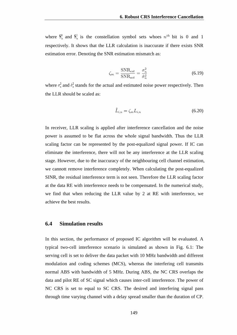
6. Robust CRS Interference Cancellation
149
where and is the constellation symbol sets whoes bit is 0 and 1
respectively. It shows that the LLR calculation is inaccurate if there exists SNR
estimation error. Denoting the SNR estimation mismatch as:
(6.19)
where and stands for the actual and estimated noise power respectively. Then
the LLR should be scaled as:
(6.20)
In receiver, LLR scaling is applied after interference cancellation and the noise
power is assumed to be flat across the whole signal bandwidth. Thus the LLR
scaling factor can be represented by the post-equalized signal power. If IC can
eliminate the interference, there will not be any interference at the LLR scaling
stage. However, due to the inaccuracy of the neighbouring cell channel estimation,
we cannott remove interference completely. When calculating the post-equalized
SINR, the residual interference term is not seen. Therefore the LLR scaling factor
at the data RE with interference needs to be compensated. In the numerical study,
we find that when reducing the LLR value by 2 at RE with interference, we
achieve the best results.
6.4 Simulation results
In this section, the performance of proposed IC algorithm will be evaluated. A
typical two-cell interference scenario is simulated as shown in Fig. 6.1: The
serving cell is set to deliver the data packet with 10 MHz bandwidth and different
modulation and coding schemes (MCS), whereas the interfering cell transmits
normal ABS with bandwidth of 5 MHz. During ABS, the NC CRS overlaps the
data and pilot RE of SC signal which causes inter-cell interference. The power of
NC CRS is set to equal to SC CRS. The desired and interfering signal pass
through time varying channel with a delay spread smaller than the duration of CP.

6. Robust CRS Interference Cancellation
150
In the simulation, the EVA [125] channel model with different Doppler frequency
is adopted to investigate the IC performance in different channel conditions. The
arriving time of desired and interfering signal is adjusted to evaluate the effect of
relative timing offset. In addition, different CFO is applied to interfering signal to
evaluate its effects. In order to generate correct PSS/SSS/CRS for IC, the user is
assumed to conducts ideal cell search. Key simulation parameters are listed below:
Table 6.1 Key Simulation Parameters Parameters Serving Cell Neighbour Cell
Bandwidth (MHz) 10 5
Antenna Port SISO/SIMO SISO
Relative Power (dB) 0 0
MCS MCS 8/16 N/A
Channel Model EVA 5/70/150/200 EVA 5/70/150/200
Channel Encoder LTE Turbo Code LTE Turbo Code
Fig. 6.5 (a)-(d) show BLER performance versus signal-to-noise ratio (SNR) in
different IC scenarios. The MCS 8 and MCS 16 are adopted. The signal is
transmitted via EVA channel with 5 Hz Doppler frequency at different SNR. The
antenna multiplex mode is set to SIMO and MIMO. The block error rate
(BLER) selected as the performance criteria, and it is calculated based on 10000
block transmissions. For comparison, the BLER of interference-free-free and
interfered transmission without IC are presented as reference in blue and grey
curves respectively. The figure also shows the performance with IC in red curve.
The effect of LLR scaling is also depicted in pink and yellow curve respectively.
By comparing the blue and grey curves in figure (a)-(d), the CRS interference
causes performance degradation during the SNR range of interest. As the red
curve shows, the proposed IC algorithm can significantly improves BLER
performance which is nearly close to the interference-free case as the red curve for
SIMO MCS 8, 16 and MIMO MCS 8. There is also considerable improvement for
MIMO MCS 16, where the BLER is whith 2 dB than ideal situation. In addition, it
can be found that LLR scaling brings some improvement after the IC. The pure
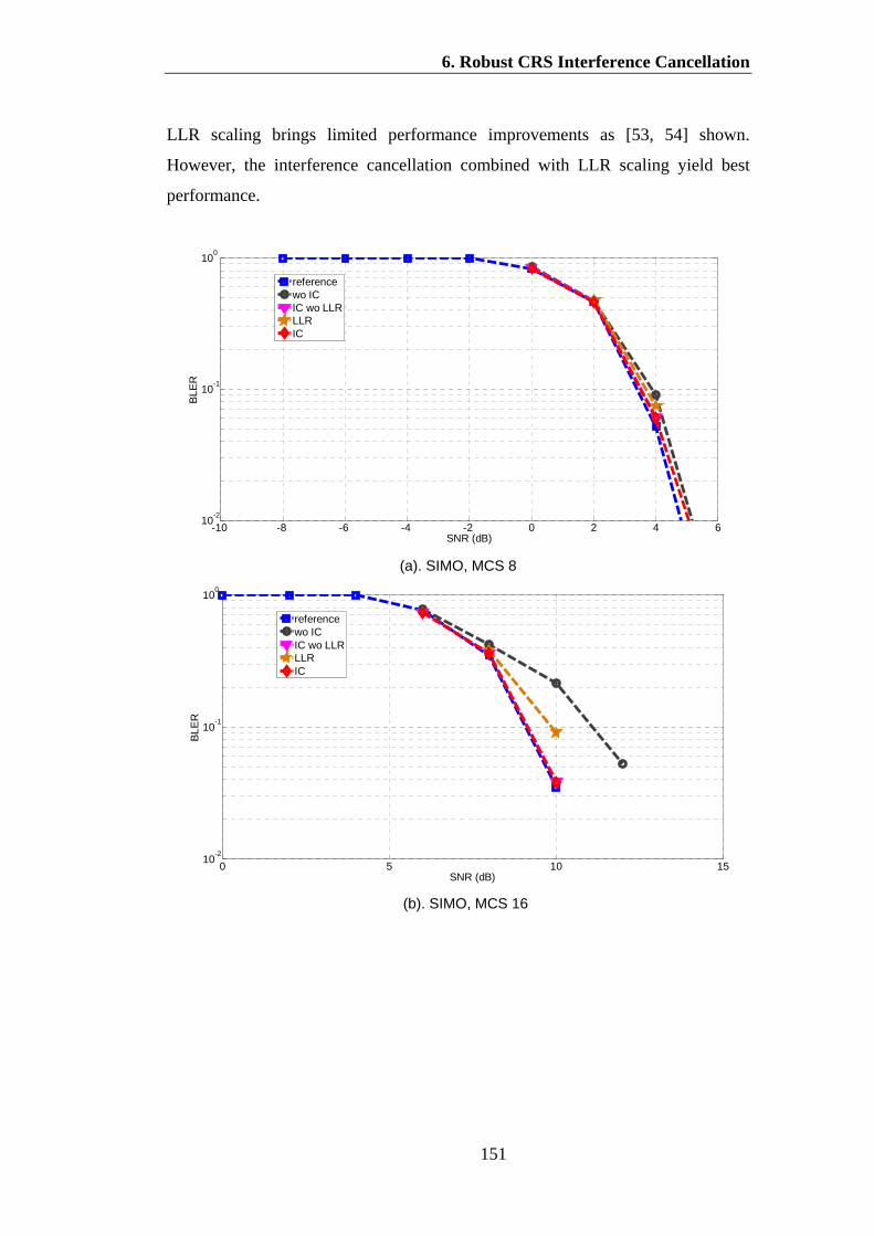
6. Robust CRS Interference Cancellation
151
LLR scaling brings limited performance improvements as [53, 54] shown.
However, the interference cancellation combined with LLR scaling yield best
performance.
(a). SIMO, MCS 8
(b). SIMO, MCS 16
-10 -8 -6 -4 -2 0 2 4 610
-2
10-1
100
SNR (dB)
BL
ER
referencewo ICIC wo LLRLLRIC
0 5 10 1510
-2
10-1
100
SNR (dB)
BL
ER
referencewo ICIC wo LLRLLRIC

6. Robust CRS Interference Cancellation
152
(c). MIMO, MCS 8
(d). MIMO, MCS 16
Figure 6.5 BLER performance versus SNR in dfferent IC scenario
Fig. 6.6 (a)–(d) show the BLER performance of different Doppler frequency
scenarios. The SIMO MCS 18 modulation is adopted in this simulation. The
Doppler frequency varies from 5 Hz to 200 Hz. The interference-free case is
presented as a reference as shown in blue curve. The performance of interfering
and IC case are shown in black and red curves respectively. According to Fig. 6.6
(a)-(b), the performance of proposed IC significantly improves the BLER
performance for different SNR and Doppler frequencies which verifies the
robustness of the IC algorithm.
4 5 6 7 8 9 10 11 12 13 1410
-2
10-1
100
SNR (dB)
BL
ER
referencewo ICIC wo LLRLLRIC
12 13 14 15 16 17 18 19 20 21 2210
-2
10-1
100
SNR (dB)
BL
ER
referencewo ICIC wo LLRLLRIC
6. Robust CRS Interference Cancellation
153
(a) 5 Hz (b) 70 Hz
(c) 150 Hz (d) 200 Hz
Figure 6.6 BLER Performance of Different Doppler Frequency Scenarios
Fig. 6.7 shows the impact of the average window length on the BLER
performance in EVA 70 Hz. As shown in Fig. 6.7, the estimate of interfering
channel is approximated by averaging M times. This is based on the
assumption that the length of moving average window is within the coherence
time of the channel, otherwise it will bring inaccuracy due to the fast varying of
the channel. In practice, this assumption is correct. This is because the UE which
is attached to femto cell and on the cell edge is more likely to be slowly moving
objects, such as pedestrian etc. High mobility objects, such as vehicles and high
speed trains etc, will be attached to large cells. For the high mobility objects are
attached femto cells, the period of attaching will be very short due to its high
mobility. Hence, this algorithm will not face high mobility channels in most of the
time. Because the statistical expectation in Eq. (6.11) is approximated by using
moving average, the window length could not be too small. The figure shows that
smaller window size gives better BLER performance. However, there will be no
6 8 10 12 14 1610
-2
10-1
100
SNR (dB)
BLE
R
referencewo ICIC
6 8 10 12 14 1610
-2
10-1
100
SNR (dB)
BLE
R
referencewo ICIC
10 12 14 16 1810
-2
10-1
100
SNR (dB)
BLE
R
referencewo ICIC
10 12 14 1610
-2
10-1
100
SNR (dB)
BLE
R
referencewo ICIC
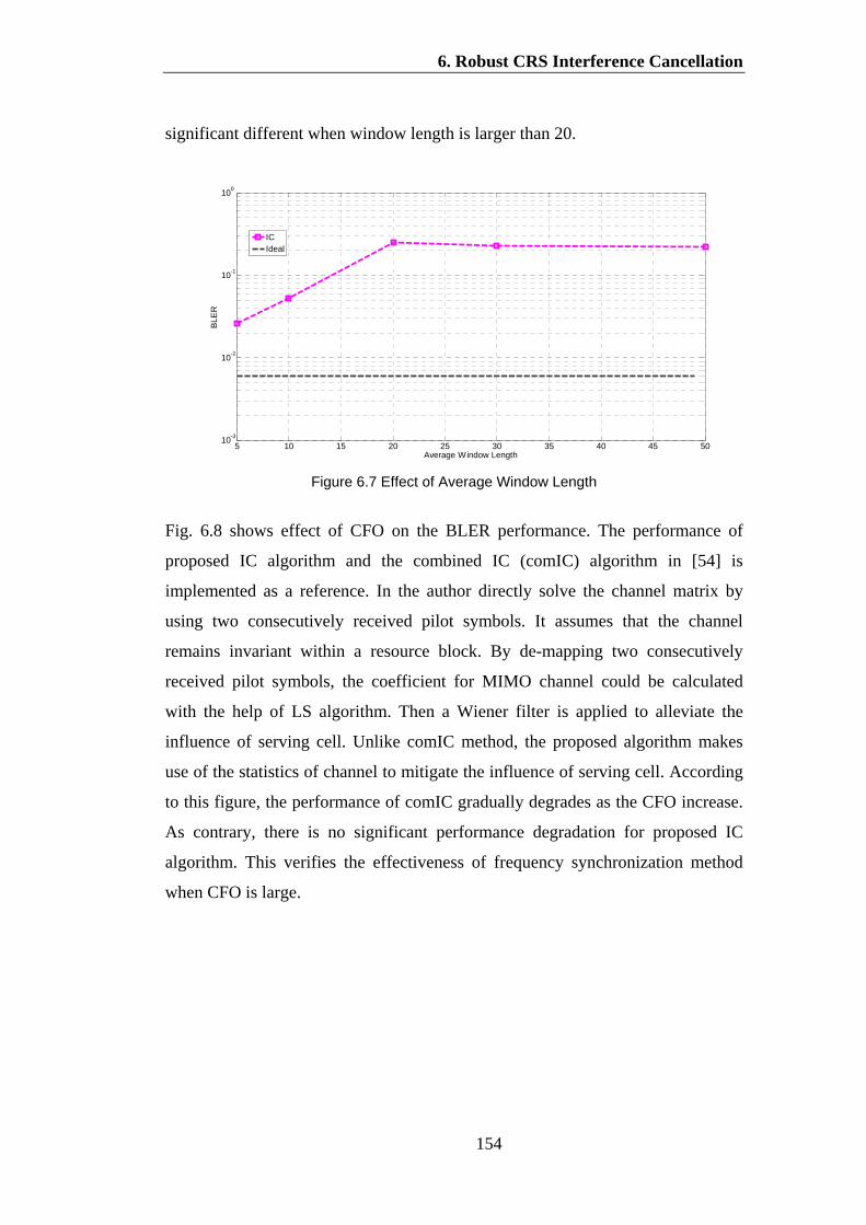
6. Robust CRS Interference Cancellation
154
significant different when window length is larger than 20.
Figure 6.7 Effect of Average Window Length
Fig. 6.8 shows effect of CFO on the BLER performance. The performance of
proposed IC algorithm and the combined IC (comIC) algorithm in [54] is
implemented as a reference. In the author directly solve the channel matrix by
using two consecutively received pilot symbols. It assumes that the channel
remains invariant within a resource block. By de-mapping two consecutively
received pilot symbols, the coefficient for MIMO channel could be calculated
with the help of LS algorithm. Then a Wiener filter is applied to alleviate the
influence of serving cell. Unlike comIC method, the proposed algorithm makes
use of the statistics of channel to mitigate the influence of serving cell. According
to this figure, the performance of comIC gradually degrades as the CFO increase.
As contrary, there is no significant performance degradation for proposed IC
algorithm. This verifies the effectiveness of frequency synchronization method
when CFO is large.
5 10 15 20 25 30 35 40 45 5010
-3
10-2
10-1
100
Average Window Length
BLE
R
ICIdeal
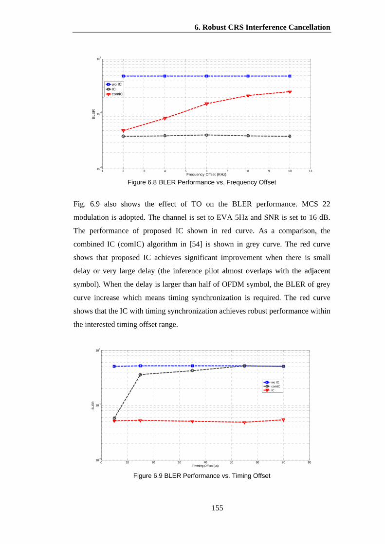
6. Robust CRS Interference Cancellation
155
Figure 6.8 BLER Performance vs. Frequency Offset
Fig. 6.9 also shows the effect of TO on the BLER performance. MCS 22
modulation is adopted. The channel is set to EVA 5Hz and SNR is set to 16 dB.
The performance of proposed IC shown in red curve. As a comparison, the
combined IC (comIC) algorithm in [54] is shown in grey curve. The red curve
shows that proposed IC achieves significant improvement when there is small
delay or very large delay (the inference pilot almost overlaps with the adjacent
symbol). When the delay is larger than half of OFDM symbol, the BLER of grey
curve increase which means timing synchronization is required. The red curve
shows that the IC with timing synchronization achieves robust performance within
the interested timing offset range.
Figure 6.9 BLER Performance vs. Timing Offset
1 2 3 4 5 6 7 8 9 10 1110
-2
10-1
100
Frequency Offset (KHz)
BLE
R
wo ICICcomIC
0 10 20 30 40 50 60 70 8010
-2
10-1
100
Timming Offset (us)
BLE
R
wo ICcomICIC
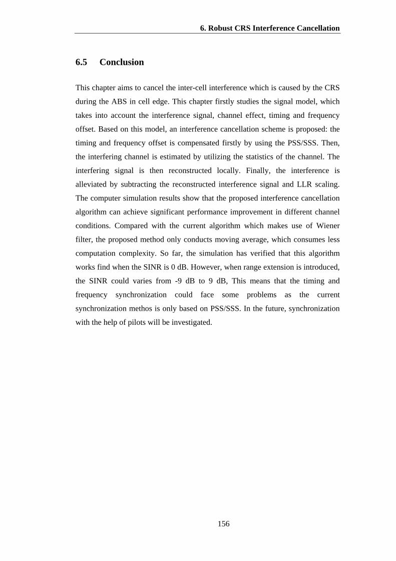
6. Robust CRS Interference Cancellation
156
6.5 Conclusion
This chapter aims to cancel the inter-cell interference which is caused by the CRS
during the ABS in cell edge. This chapter firstly studies the signal model, which
takes into account the interference signal, channel effect, timing and frequency
offset. Based on this model, an interference cancellation scheme is proposed: the
timing and frequency offset is compensated firstly by using the PSS/SSS. Then,
the interfering channel is estimated by utilizing the statistics of the channel. The
interfering signal is then reconstructed locally. Finally, the interference is
alleviated by subtracting the reconstructed interference signal and LLR scaling.
The computer simulation results show that the proposed interference cancellation
algorithm can achieve significant performance improvement in different channel
conditions. Compared with the current algorithm which makes use of Wiener
filter, the proposed method only conducts moving average, which consumes less
computation complexity. So far, the simulation has verified that this algorithm
works find when the SINR is 0 dB. However, when range extension is introduced,
the SINR could varies from -9 dB to 9 dB, This means that the timing and
frequency synchronization could face some problems as the current
synchronization methos is only based on PSS/SSS. In the future, synchronization
with the help of pilots will be investigated.

161
7. Conclusions
7.1 Discussions
In this dissertation, techniques for performance enhancement of LTE and beyond
systems are studied. On the transmitter side, a self-IQ-demodulation based
compensation scheme for FD I/Q imbalance is proposed. This scheme makes use
of a power detection circuit of the generic DCT and deigns a special test signal.
The signal and controlled LO leakage is transmitted first. The RF signal
modulates itself in the diode and generates a baseband signal which carries the FD
I/Q imbalance information. The training signal and LO is transmitted in a “time
division” way which realizes self-IQ-demodulation. The I/Q imbalance parameter
is resolved from the demodulated complex valued baseband data.
At the receiver side, an optimum OFDM receiver is designed to cope with the
STO, CFO, SFO, and the doubly selective channel. The impact of CFO, STO and
fading channel is mitigated in the coarse estimation stage where low computation
hybrid algorithms are adopted. The dominant STO and CFO are firstly eliminated
by the CP-based algorithm and the CFR is estimated by LS algorithm. Further to
this, the residual CFO and SFO are eliminated using a pilot-based correlation
method in the fine estimation stage. In order to combat the impact of residual
frequency error and imperfection channel estimation caused by Doppler shift, a
low computationally complex MMSE-DFE is developed. Moreover, a FPGA-
based co-simulation platform is developed. This combines the advantages of
MATLAB and FPGA, which speeds up the algorithm verification process.
A subspace-based SNR estimation algorithm is proposed for this receiver. This
algorithm estimates the power in the signal space and noise space respectively and
provides an accurate SNR estimates for the reliable equalizer and AMC. In order
to mitigate the interference from neighbouring cells, the receiver also includes a

7. Conclusions
158
new CRS interference cancellation scheme. In this scheme, the CRS interference
is cancelled with the help of SC data and channel statistics. LLR enhancement
helps to improve the BLER performance. The impact of STO and CFO from NC
is alleviated.
Compared with conventional techniques, this dissertation generally makes several
improvements in terms of performance, cost and computational complexity. The
proposed self-IQ-demodulation based compensation scheme yields a 50dB IRR
which meets the requirements of most wideband systems. The conventional
method manually calibrates the I/Q imbalance with the help of external
instruments which is expensive and low in efficiency. By contrast, the proposed
self-IQ-demodulation based compensation scheme only utilizes the internal diode
and ADC and the calibration can be realized automatically with 10dB IRR
improvement. This reduces the hardware cost and increases calibration efficiency.
The optimum OFDM receiver adopts several classical estimation algorithms and
achieves typical EVM performance of 1.9% at SNR of 20 dB for 16QAM. The
newly derived MMSE-DFE avoids the Cholesky decomposition in conventional
MMSE-DFE by optimizing the cost function and only requires 5N multiplication
operations and 3N addition operations. The sub-space based SNR estimation
algorithm yielding estimation error stays below 0.09 even when it works in high
mobility channels, whereas the conventional moving average methods become
ineffective. It flexibly adjusts the decomposed signal and noise space, which
makes it suitable for time-variant channel and flexible pilot allocation scenarios in
LTE/beyond systems. In addition, the FPGA based co-simulation platform adopts
universal data interface which makes it flexible to implement algorithm in FPGA.
Co-simulation with hardware in chain speeds up the whole algorithm verification
process.
For this proposed CRS interference cancellation algorithm, it improves the
robustness when CFO and STO appear and the performance is enhanced by LLR
puncturing compared with conventional algorithms.

7. Conclusions
159
7.2 Further work
In this thesis, LTE/beyond system performance enhancement techniques are
theoretically investigated. A low cost FD transmitter I/Q imbalance compensation
scheme is proposed leading to satisfactory IRR improvement. An optimum
OFDM receiver is designed which reduces computational complexity and is
suitable for hardware implementation. The CRS interference cancellation
performance is also refined.
However, some improvements can be achieved with a future work:
1). I/Q imbalance estimation methods: The current estimation is based on
digitized RF data from an 8 bit oscilloscope which hampers the estimation
accuracy. And the higher order effect of the diode is simulated in MATLAB.
Though it achieves a satisfactory result, performance needs to be verified In
practice. Hence, the first stage could be conducting the experiment on a real wide
band diode. Furthermore, a multiplier could be applied in the feedback path where
the LO can be directly used for I/Q demodulation. The introduction of a multiplier
is expected to significantly reduce harmonics and other interferences. Hence,
other non-linear distortion could be estimated. Tthe second stage could be
introducing a multiplier in the feedback path and developing automatic calibration
algorithms for other non-linear distortions.
2). Receiver timing and frequency synchronization algorithm: The current
receiver algorithm mitigates the impact of STO and CFO with the help of CP
correlation. It is suitable for CP OFDM systems. Further LTE systems, isotropic
orthogonal transform algorithm (IOTA) could be adopted which contains no CP
[136]. Hence, more compatible timing and frequency synchronization algorithms
need to be developed.

7. Conclusions
160
3). CRS interference cancellation: The current CRS interference cancellation
assumes only one NC contributes to the interference. However, more cells will be
deployed in further LTE releases which means more interfering cells. In this
context, cancellation algorithms that can search for interfering cell and cancel
interference from a specific cell are needed. In addition, the current interference
cancellation assuming that cells search for interfering cell is correct. However, the
synchronization channel from different cells overlaps, making it difficult to
decode the cell ID. Hence, a reliable cell search in the interfering scenario is also
needed. To summarize, further work on CRS interference cancellation would be:
A). Develop a multi-cell CRS interference cancellation algorithm. As the timing
and frequency estimation could be inaccurate when SNR, future work will include
accurate timing and frequency synchronization by making use of pilot symbols.
B). Develop a reliable cell search algorithm when several interfering cells are
active.
161
Reference
[1] ITU. (2014). Key 2005-2014 ICT data for the world by geographic regions and by level of development. Available: http://www.itu.int/en/ITU-D/Statistics/Pages/stat/default.aspx?utm_source=twitterfeed&utm_medium=twitter.co.jp
[2] Y. Chen, "Soft Handover Issues in Radio Resource Management for 3G WCDMA Networks," 2003.
[3] C. K. Toh, Ad hoc mobile wireless networks: protocols and systems: Pearson Education, 2001.
[4] A. Electronics. 2G – 3G Cellular Wireless data transport terminology, . Available: http://www.arcelect.com/2G-3G_Cellular_Wireless.htm
[5] D. Astely, E. Dahlman, G. Fodor, S. Parkvall, and J. Sachs, "LTE release 12 and beyond," Communications Magazine, IEEE, vol. 51, pp. 154-160, 2013.
[6] J.-S. Lee, Y.-W. Su, and C.-C. Shen, "A comparative study of wireless protocols: Bluetooth, UWB, ZigBee, and Wi-Fi," in Industrial Electronics Society, 2007. IECON 2007. 33rd Annual Conference of the IEEE, 2007, pp. 46-51.
[7] C. Evans-Pughe, "Bzzzz zzz [ZigBee wireless standard]," IEE Review, vol. 49, pp. 28-31, 2003.
[8] S. Fiehe, J. Riihijärvi, and P. Mähönen, "Experimental Study on Performance of IEEE 802.11 n and Impact of Interferers on the 2.4 GHz ISM Band," in Proceedings of the 6th International Wireless Communications and Mobile Computing Conference, 2010, pp. 47-51.
[9] 802.16.1a-2013. IEEE Standard for WirelessMAN-Advanced Air Interface for Broadband Wireless Access Systems --Amendment 2: Higher Reliability Networks. Available: http://standards.ieee.org/findstds/standard/802.16.1a-2013.html
[10] 3GPP TS 36.814, "Evolved Universal Terrestrial Radio Access (E-UTRA); Further advancements for E-UTRA physical layer aspects (Release 9)," v. 9.0.0 Mar. 2010.
[11] E. U. T. R. Access, "and Evolved Universal Terrestrial Radio Access Network (E-UTRAN); Overall description; Stage 2 (Release 10), 3GPP Technical Specification TS 36.300 V10. 2.0, Dec. 2010," ed.

Reference
162
[12] P. Bhat, S. Nagata, L. Campoy, I. Berberana, T. Derham, L. Guangyi, et al., "LTE-advanced: an operator perspective," Communications Magazine, IEEE, vol. 50, pp. 104-114, 2012.
[13] J. K. Cavers and M. W. Liao, "Adaptive compensation for imbalance and offset losses in direct conversion transceivers," Vehicular Technology, IEEE Transactions on, vol. 42, pp. 581-588, 1993.
[14] J. Crols and M. S. J. Steyaert, "Low-IF topologies for high-performance analog front ends of fully integrated receivers," Circuits and Systems II: Analog and Digital Signal Processing, IEEE Transactions on, vol. 45, pp. 269-282, 1998.
[15] D. S. Hilborn, S. P. Stapleton, and J. K. Cavers, "An adaptive direct conversion transmitter," Vehicular Technology, IEEE Transactions on, vol. 43, pp. 223-233, 1994.
[16] B. Razavi, "Design considerations for direct-conversion receivers," Circuits and Systems II: Analog and Digital Signal Processing, IEEE Transactions on, vol. 44, pp. 428-435, 1997.
[17] M. Valkama, M. Renfors, and V. Koivunen, "Advanced methods for I/Q imbalance compensation in communication receivers," Signal Processing, IEEE Transactions on, vol. 49, pp. 2335-2344, 2001.
[18] L. Anttila, M. Valkama, and M. Renfors, "Frequency-Selective <emphasis>I/Q</emphasis> Mismatch Calibration of Wideband Direct-Conversion Transmitters," Circuits and Systems II: Express Briefs, IEEE Transactions on, vol. 55, pp. 359-363, 2008.
[19] K. Minseok, Y. Maruichi, and J. Takada, "Parametric Method of Frequency-Dependent I/Q Imbalance Compensation for Wideband Quadrature Modulator," Microwave Theory and Techniques, IEEE Transactions on, vol. 61, pp. 270-280, 2013.
[20] P. Mathecken, T. Riihonen, S. Werner, and R. Wichman, "Performance Analysis of OFDM with Wiener Phase Noise and Frequency Selective Fading Channel," Communications, IEEE Transactions on, vol. 59, pp. 1321-1331, 2011.
[21] T. M. Schmidl and D. C. Cox, "Robust frequency and timing synchronization for OFDM," Communications, IEEE Transactions on, vol. 45, pp. 1613-1621, 1997.
[22] M. Faulkner, T. Mattsson, and W. Yates, "Automatic adjustment of quadrature modulators," Electronics Letters, vol. 27, pp. 214-216, 1991.
[23] R. Marchesani, "Digital precompensation of imperfections in quadrature modulators," Communications, IEEE Transactions on, vol. 48, pp. 552-556, 2000.

Reference
163
[24] H. Xinping and M. Caron, "Efficient Transmitter Self-Calibration and Amplifier Linearization Techniques," in Circuits and Systems, 2007. ISCAS 2007. IEEE International Symposium on, 2007, pp. 265-268.
[25] J. Tuthill and A. Cantoni, "Efficient compensation for frequency-dependent errors in analog reconstruction filters used in IQ modulators," Communications, IEEE Transactions on, vol. 53, pp. 489-496, 2005.
[26] D. Lei, M. Zhengxiang, D. R. Morgan, M. Zierdt, and G. T. Zhou, "Frequency-dependent modulator imbalance in predistortion linearization systems: modeling and compensation," in Signals, Systems and Computers, 2004. Conference Record of the Thirty-Seventh Asilomar Conference on, 2003, pp. 688-692 Vol.1.
[27] S. A. Leyonhjelm and M. Faulkner, "The effect of reconstruction filters on direct upconversion in a multichannel environment," Vehicular Technology, IEEE Transactions on, vol. 44, pp. 95-102, 1995.
[28] M. Windisch and G. Fettweis, "Adaptive I/Q imbalance compensation in low-IF transmitter architectures," in Vehicular Technology Conference, 2004. VTC2004-Fall. 2004 IEEE 60th, 2004, pp. 2096-2100 Vol. 3.
[29] S. Burglechner, G. Hueber, and A. Springer, "On the estimation and compensation of IQ impairments in direct conversion transmitters," in Wireless Technology, 2008. EuWiT 2008. European Conference on, 2008, pp. 69-72.
[30] A. J. Goldsmith and P. P. Varaiya, "Capacity of fading channels with channel side information," Information Theory, IEEE Transactions on, vol. 43, pp. 1986-1992, 1997.
[31] L. J. Cimini, "Analysis and simulation of a digital mobile channel using orthogonal frequency division multiplexing," Communications, IEEE Transactions on, vol. 33, pp. 665-675, 1985.
[32] W. Jakes, "Microwave Mobile Channels," New York: Wiley, vol. 2, pp. 159-176, 1974.
[33] P. Schniter, "Low-complexity equalization of OFDM in doubly selective channels," Signal Processing, IEEE Transactions on, vol. 52, pp. 1002-1011, 2004.
[34] T. Strohmer and S. Beaver, "Optimal OFDM design for time-frequency dispersive channels," Communications, IEEE Transactions on, vol. 51, pp. 1111-1122, 2003.
[35] M. Rupp, C. Mehlführer, and M. Wrulich, Evaluation of HSDPA and LTE: from testbed measurements to system level performance: John Wiley & Sons, 2011.

Reference
164
[36] N.-L. Hung, T. Le-Ngoc, and K. Chi-Chung, "RLS-Based Joint Estimation and Tracking of Channel Response, Sampling, and Carrier Frequency Offsets for OFDM," Broadcasting, IEEE Transactions on, vol. 55, pp. 84-94, 2009.
[37] N.-L. Hung, T. Le-Ngoc, and N. H. Tran, "Iterative Receiver Design With Joint Doubly Selective Channel and CFO Estimation for Coded MIMO-OFDM Transmissions," Vehicular Technology, IEEE Transactions on, vol. 60, pp. 4052-4057, 2011.
[38] C. Jianwu, W. Yik-Chung, M. Shaodan, and N. Tung-Sang, "Joint CFO and Channel Estimation for Multiuser MIMO-OFDM Systems With Optimal Training Sequences," Signal Processing, IEEE Transactions on, vol. 56, pp. 4008-4019, 2008.
[39] M. Speth, S. A. Fechtel, G. Fock, and H. Meyr, "Optimum receiver design for wireless broad-band systems using OFDM. I," Communications, IEEE Transactions on, vol. 47, pp. 1668-1677, 1999.
[40] M. Speth, S. Fechtel, G. Fock, and H. Meyr, "Optimum receiver design for OFDM-based broadband transmission .II. A case study," Communications, IEEE Transactions on, vol. 49, pp. 571-578, 2001.
[41] K. Feher, Advanced digital communications: systems and signal processing techniques: Noble Publishing Corporation, 1997.
[42] N. Al-Dhahir and J. M. Cioffi, "Block transmission over dispersive channels: transmit filter optimization and realization, and MMSE-DFE receiver performance," Information Theory, IEEE Transactions on, vol. 42, pp. 137-160, 1996.
[43] A. Stamoulis, G. B. Giannakis, and A. Scaglione, "Block FIR decision-feedback equalizers for filterbank precoded transmissions with blind channel estimation capabilities," Communications, IEEE Transactions on, vol. 49, pp. 69-83, 2001.
[44] D. Williamson, R. A. Kennedy, and G. W. Pulford, "Block decision feedback equalization," Communications, IEEE Transactions on, vol. 40, pp. 255-264, 1992.
[45] H. Shousheng and M. Torkelson, "Effective SNR estimation in OFDM system simulation," in Global Telecommunications Conference, 1998. GLOBECOM 1998. The Bridge to Global Integration. IEEE, 1998, pp. 945-950 vol.2.
[46] H. Abeida, "Data-Aided SNR Estimation in Time-Variant Rayleigh Fading Channels," Signal Processing, IEEE Transactions on, vol. 58, pp. 5496-5507, 2010.
Reference
165
[47] X. Xiaodong, J. Ya, and Y. Xiaohu, "Subspace-based noise variance and SNR estimation for OFDM systems " in Wireless Communications and Networking Conference, 2005 IEEE, 2005, pp. 23-26 Vol. 1.
[48] A. Khandekar, N. Bhushan, T. Ji, and V. Vanghi, "LTE-Advanced: Heterogeneous networks," in Wireless Conference (EW), 2010 European, 2010, pp. 978-982.
[49] A. Damnjanovic, J. Montojo, W. Yongbin, J. Tingfang, L. Tao, M. Vajapeyam, et al., "A survey on 3GPP heterogeneous networks," Wireless Communications, IEEE, vol. 18, pp. 10-21, 2011.
[50] S. Parkvall, A. Furuskar, and E. Dahlman, "Evolution of LTE toward IMT-advanced," Communications Magazine, IEEE, vol. 49, pp. 84-91, 2011.
[51] 3GPP R1-105335, "Details of almost blank subframes," Ericsson STEricsson,Oct. 2010.
[52] Qualcomm Inc. R4-102350, "Enabling communication in harsh interference scenarios," 3GPP-RAN WG4 AH#10-03, Bratislava, Jul. 2010.
[53] Qualcomm Inc R4-123313, "Link level simulations for FeICIC with 9dB cell range expansion," 3GPP-RAN WG4 #63, Prague, May 2012.
[54] H. Ming and X. Wen, "Macro-femto inter-cell interference mitigation for 3GPP LTE-A downlink," in Wireless Communications and Networking Conference Workshops (WCNCW), 2012 IEEE, 2012, pp. 75-80.
[55] B. E. Priyanto, S. Kant, F. Rusek, H. Sha, C. Jianjun, and C. Wugengshi, "Robust UE Receiver with Interference Cancellation in LTE Advanced Heterogeneous Network," in Vehicular Technology Conference (VTC Fall), 2013 IEEE 78th, 2013, pp. 1-7.
[56] 3GPP TS 36.211, "Evolved Universal Terrestrial Radio Access (E-UTRA): Physical channels and modulation," v 10.0.0 Dec. 2011.
[57] A. A. Abidi, "Direct-conversion radio transceivers for digital communications," Solid-State Circuits, IEEE Journal of, vol. 30, pp. 1399-1410, 1995.
[58] M. Suarez, O. Zlydareva, and E. P. Ling, "LTE/WiMAX multimode mobile transceiver, comparison of performances and power efficiency issues," in Aerospace Conference, 2013 IEEE, 2013, pp. 1-10.
[59] B. Razavi, "Challenges in portable RF transceiver design," Circuits and Devices Magazine, IEEE, vol. 12, pp. 12-25, 1996.

Reference
166
[60] L. Noor and A. Anpalagan, "Direct conversion receiver for radio communication systems," Potentials, IEEE, vol. 24, pp. 32-35, 2005.
[61] K. Martin, "Complex signal processing is not-complex," in Circuits and Systems, 2004. MWSCAS '04. The 2004 47th Midwest Symposium on, 2004, pp. xvi-xvi.
[62] N. Zimmermann, Design and implementation of a broadband RF-DAC transmitter for wireless communications: Universitätsbibliothek, 2011.
[63] J. G. Proakis, "Digital communications, 1995," ed: McGraw-Hill, New York.
[64] H. Hashemi, "Impulse response modeling of indoor radio propagation channels," Selected Areas in Communications, IEEE Journal on, vol. 11, pp. 967-978, 1993.
[65] E. U. T. R. Access, "Multiplexing and channel coding (Release 9). 3GPP Organizational Partners TS 36.212 Rev. 8.3. 0," ed: May, 2008.
[66] M. Pelcat, "Rapid prototyping and dataflow-based code generation for the 3GPP LTE enodeb physical layer mapped onto multi-core DSPs," Ph. D. dissertation, Dissertation, INSA Rennes, 210 p, 2010.
[67] A. Ghosh, R. Ratasuk, B. Mondal, N. Mangalvedhe, and T. Thomas, "LTE-advanced: next-generation wireless broadband technology [Invited Paper]," Wireless Communications, IEEE, vol. 17, pp. 10-22, 2010.
[68] P. Garcia, A. Ortega, J. De Mingo, and A. Valdovinos, "Nonlinear distortion cancellation in OFDM systems using an adaptive LINC structure," in Personal, Indoor and Mobile Radio Communications, 2004. PIMRC 2004. 15th IEEE International Symposium on, 2004, pp. 1506-1510 Vol.2.
[69] Z. W. Zheng, Y. Zhi-Xing, P. Chang-Yong, and Y.-S. Zhu, "Effects of nonlinear distortion and imperfect parameters estimation on the performance of OFDM-based DTTB systems," Broadcasting, IEEE Transactions on, vol. 51, pp. 237-243, 2005.
[70] A. Chini, W. Yiyan, M. El-Tanany, and S. Mahmoud, "Hardware nonlinearities in digital TV broadcasting using OFDM modulation," Broadcasting, IEEE Transactions on, vol. 44, pp. 12-21, 1998.
[71] I. T. Lu and C. Jiang, "Joint transmitter and receiver IQ imbalance estimation and compensation for OFDM systems," in Radio and Wireless Symposium (RWS), 2010 IEEE, 2010, pp. 476-479.
[72] S. Kexuan, I. Darwazeh, H. Li-Ke, and A. Jones, "Optimal pilot based frequency-dependent I/Q imbalance compensation for wideband direct-

Reference
167
conversion transmitters," in Wireless Communications and Networking Conference (WCNC), 2012 IEEE, 2012, pp. 226-231.
[73] A. Nassery, S. Byregowda, S. Ozev, M. Verhelst, and M. Slamani, "Built-In Self-Test of Transmitter I/Q Mismatch and Nonlinearity Using Self-Mixing Envelope Detector," Very Large Scale Integration (VLSI) Systems, IEEE Transactions on, vol. 23, pp. 331-341, 2015.
[74] G.-J. Van Rooyen, "Baseband compensation principles for defects in quadrature signal conversion and processing," University of Stellenbosch, 2005.
[75] P. Kiss and V. Prodanov, "One-tap wideband I/Q compensation for zero-IF filters," Circuits and Systems I: Regular Papers, IEEE Transactions on, vol. 51, pp. 1062-1074, 2004.
[76] L. Chia-Liang, "Impacts Of I/q Imbalance On Qpsk-ofdm-qam Detection," in Consumer Electronics, 1998. ICCE. 1998 Digest of Technical Papers. International Conference on, 1998, pp. 384-385.
[77] A. G. K. C. Lim, V. Sreeram, and W. Guo-Qing, "Digital compensation in IQ modulators using adaptive FIR filters," Vehicular Technology, IEEE Transactions on, vol. 53, pp. 1809-1817, 2004.
[78] J. Tuthill and A. Cantoni, "Optimum precompensation filters for IQ modulation systems," Communications, IEEE Transactions on, vol. 47, pp. 1466-1468, 1999.
[79] M. Valkama, Advanced I/Q signal processing for wideband receivers: Models and algorithms, 2001.
[80] B. Vargha, J. Schoukens, and Y. Rolain, "Static nonlinearity testing of D/A converters," in Instrumentation and Measurement Technology Conference, 2001. IMTC 2001. Proceedings of the 18th IEEE, 2001, pp. 1684-1689 vol.3.
[81] J. J. De Witt, "Modelling, estimation and compensation of imbalances in quadrature transceivers," PhD, University of Stellenbosch, 2011.
[82] L. Ding, M. Zhengxiang, D. R. Morgan, M. Zierdt, and G. T. Zhou, "Compensation of Frequency-Dependent Gain/Phase Imbalance in Predistortion Linearization Systems," Circuits and Systems I: Regular Papers, IEEE Transactions on, vol. 55, pp. 390-397, 2008.
[83] L. Anttila, P. Handel, and M. Valkama, "Joint Mitigation of Power Amplifier and I/Q Modulator Impairments in Broadband Direct-Conversion Transmitters," Microwave Theory and Techniques, IEEE Transactions on, vol. 58, pp. 730-739, 2010.
Reference
168
[84] U. Mengali and A. N. D'Andrea, Synchronization techniques for digital receivers: Springer, 1997.
[85] S. S. Haykin, Adaptive filter theory: Pearson Education India, 2008.
[86] V. P. G. Jiménez, Y. Jabrane, A. G. Armada, B. A. E. Said, and A. A. Ouahman, "High power amplifier pre-distorter based on neural-fuzzy systems for OFDM signals," Broadcasting, IEEE Transactions on, vol. 57, pp. 149-158, 2011.
[87] A. Prochazka and R. Neumann, "High Frequency Distortion Analysis of a Semiconductor Diode for CATV Applications," Consumer Electronics, IEEE Transactions on, vol. CE-21, pp. 120-130, 1975.
[88] R. W. Lucky, "Automatic equalization for digital communication," Bell System Technical Journal, The, vol. 44, pp. 547-588, 1965.
[89] A. Bo, Y. Zhi-Xing, P. Chang-Yong, G. Jian-hua, W. Yong, and L. Zhen, "On the synchronization techniques for wireless OFDM systems," Broadcasting, IEEE Transactions on, vol. 52, pp. 236-244, 2006.
[90] W. Lu, Z. Xian-Da, L. Pei-Sheng, and S. Yong-Tao, "A closed-form blind CFO estimator based on frequency analysis for OFDM systems," Communications, IEEE Transactions on, vol. 57, pp. 1634-1637, 2009.
[91] L. Jian, L. Guoqing, and G. B. Giannakis, "Carrier frequency offset estimation for OFDM-based WLANs," Signal Processing Letters, IEEE, vol. 8, pp. 80-82, 2001.
[92] H. Defeng and K. B. Letaief, "Carrier frequency offset estimation for OFDM systems using subcarriers," Communications, IEEE Transactions on, vol. 54, pp. 813-823, 2006.
[93] W. Zhu, Y. Li, X. Zhou, and J. Yu, "Blind Channel Estimation Algorithm with Simplified Implementation for OFDM System," in Networks Security Wireless Communications and Trusted Computing (NSWCTC), 2010 Second International Conference on, 2010, pp. 274-277.
[94] S. Ghadrdan, M. Ahmadian, S. Salari, and M. Heydarzadeh, "An improved blind channel estimation algorithm for OFDM systems," in Telecommunications (IST), 2010 5th International Symposium on, 2010, pp. 421-425.
[95] S. Coleri, M. Ergen, A. Puri, and A. Bahai, "Channel estimation techniques based on pilot arrangement in OFDM systems," Broadcasting, IEEE Transactions on, vol. 48, pp. 223-229, 2002.
[96] T. Hrycak, S. Das, G. Matz, and H. G. Feichtinger, "Practical Estimation of Rapidly Varying Channels for OFDM Systems," Communications, IEEE Transactions on, vol. 59, pp. 3040-3048, 2011.

Reference
169
[97] K. Yong-Hwa and L. Jong-Ho, "Joint Maximum Likelihood Estimation of Carrier and Sampling Frequency Offsets for OFDM Systems," Broadcasting, IEEE Transactions on, vol. 57, pp. 277-283, 2011.
[98] M. Morelli and M. Moretti, "Fine carrier and sampling frequency synchronization in OFDM systems," Wireless Communications, IEEE Transactions on, vol. 9, pp. 1514-1524, 2010.
[99] S. U. Qureshi, "Adaptive equalization," Proceedings of the IEEE, vol. 73, pp. 1349-1387, 1985.
[100] S. Haykin, Communication systems: John Wiley & Sons, 2008.
[101] K. Shi, E. Serpedin, and P. Ciblat, "Decision-directed fine synchronization in OFDM systems," Communications, IEEE Transactions on, vol. 53, pp. 408-412, 2005.
[102] A. Stamoulis, S. N. Diggavi, and N. Al-Dhahir, "Estimation of fast fading channels in OFDM," in Wireless Communications and Networking Conference, 2002. WCNC2002. 2002 IEEE, 2002, pp. 465-470.
[103] G. De Michell and R. K. Gupta, "Hardware/software co-design," Proceedings of the IEEE, vol. 85, pp. 349-365, 1997.
[104] S. Haykin, "Cognitive radio: brain-empowered wireless communications," Selected Areas in Communications, IEEE Journal on, vol. 23, pp. 201-220, 2005.
[105] K. Amiri, S. Yang, P. Murphy, C. Hunter, J. R. Cavallaro, and A. Sabharwal, "WARP, a Unified Wireless Network Testbed for Education and Research," in Microelectronic Systems Education, 2007. MSE '07. IEEE International Conference on, 2007, pp. 53-54.
[106] F. Classen, Systemkomponenten für eine terrestrische digitale mobile Breitbandübertragung: Dissertation: Shaker, 1996.
[107] M. Morelli, C. C. J. Kuo, and P. Man-On, "Synchronization Techniques for Orthogonal Frequency Division Multiple Access (OFDMA): A Tutorial Review," Proceedings of the IEEE, vol. 95, pp. 1394-1427, 2007.
[108] S. Wu and Y. Bar-Ness, "OFDM channel estimation in the presence of frequency offset and phase noise," in Communications, 2003. ICC '03. IEEE International Conference on, 2003, pp. 3366-3370 vol.5.
[109] K. Manolakis, D. M. Gutierrez Estevez, V. Jungnickel, W. Xu, and C. Drewes, "A Closed Concept for Synchronization and Cell Search in 3GPP LTE Systems," in Wireless Communications and Networking Conference, 2009. WCNC 2009. IEEE, 2009, pp. 1-6.

Reference
170
[110] R. Tesi, M. Hamalainen, and J. Iinatti, "Channel Estimation Algorithms Comparison for Multiband-OFDM," in Personal, Indoor and Mobile Radio Communications, 2006 IEEE 17th International Symposium on, 2006, pp. 1-5.
[111] V. K. Jones and G. C. Raleigh, "Channel estimation for wireless OFDM systems," in Global Telecommunications Conference, 1998. GLOBECOM 1998. The Bridge to Global Integration. IEEE, 1998, pp. 980-985 vol.2.
[112] Y. Young-Hwan, K. Joonbeom, and S. Hyoung-Kyu, "Pilot-Assisted Fine Frequency Synchronization for OFDM-Based DVB Receivers," Broadcasting, IEEE Transactions on, vol. 55, pp. 674-678, 2009.
[113] H. Meng-Han and W. Che-Ho, "Channel estimation for OFDM systems based on comb-type pilot arrangement in frequency selective fading channels," Consumer Electronics, IEEE Transactions on, vol. 44, pp. 217-225, 1998.
[114] L. Rugini, P. Banelli, R. C. Cannizzaro, and G. Leus, "Channel Estimation and Windowed DEF for OFDM with Doppler Spread," in Acoustics, Speech and Signal Processing, 2006. ICASSP 2006 Proceedings. 2006 IEEE International Conference on, 2006, pp. IV-IV.
[115] L. Favalli, P. Savazzi, and S. Somma, "Improved Block DFE Equalization for Mobile WiMAX OFDM Systems," in Global Telecommunications Conference, 2007. GLOBECOM '07. IEEE, 2007, pp. 3384-3388.
[116] S. Tomasin and N. Benvenuto, "A reduced complexity block iterative DFE for dispersive wireless applications," in Vehicular Technology Conference, 2004. VTC2004-Fall. 2004 IEEE 60th, 2004, pp. 1693-1697 Vol. 3.
[117] J. J. van de Beek, O. Edfors, M. Sandell, S. K. Wilson, and P. Ola Borjesson, "On channel estimation in OFDM systems," in Vehicular Technology Conference, 1995 IEEE 45th, 1995, pp. 815-819 vol.2.
[118] A. Ijaz, A. B. Awoseyila, and B. G. Evans, "Signal-to-Noise Ratio Estimation Algorithm for Advanced DVB-RCS Systems," Broadcasting, IEEE Transactions on, vol. 58, pp. 603-608, 2012.
[119] A. Wiesel, J. Goldberg, and H. Messer-Yaron, "SNR estimation in time-varying fading channels," Communications, IEEE Transactions on, vol. 54, pp. 841-848, 2006.
[120] G. T. R4-000020, "Simulation Results of CPICH RSCP/RSSI vrs. CPICH RSCP/ISCP," Jan 2000.
[121] J. Heiskala and J. Terry Ph D, OFDM wireless LANs: A theoretical and practical guide: Sams, 2001.

Reference
171
[122] J. G. Proakis, Digital signal processing: principles algorithms and applications: Pearson Education India, 2001.
[123] M. Wax and T. Kailath, "Detection of signals by information theoretic criteria," Acoustics, Speech and Signal Processing, IEEE Transactions on, vol. 33, pp. 387-392, 1985.
[124] M. A. R. Khan and D. S. Poskitt, "Description length based signal detection in singular spectrum analysis," Monash Econometrics and Business Statistics Working Papers, vol. 13, 2010.
[125] 3GPP TS 36.101, "Evolved universal terrestrial radio access (E-UTRA), user equipment (UE) radio transmission and reception," v .11.0 Mar. 2012.
[126] K. W. Cheung and S. W. Cheung, "Super-resolving multipath channels using modified MDL," Electronics Letters, vol. 34, pp. 43-45, 1998.
[127] S. N. S. Kshatriya, S. Kaimalettu, S. R. Yerrapareddy, K. Milleth, and N. Akhtar, "On interference management based on subframe blanking in Heterogeneous LTE networks," in Communication Systems and Networks (COMSNETS), 2013 Fifth International Conference on, 2013, pp. 1-7.
[128] S. Deb, P. Monogioudis, J. Miernik, and J. P. Seymour, "Algorithms for Enhanced Inter-Cell Interference Coordination (eICIC) in LTE HetNets," Networking, IEEE/ACM Transactions on, vol. 22, pp. 137-150, 2014.
[129] J. J. van de Beek, M. Sandell, and P. O. Borjesson, "ML estimation of time and frequency offset in OFDM systems," Signal Processing, IEEE Transactions on, vol. 45, pp. 1800-1805, 1997.
[130] M. Speth, D. Daecke, and H. Meyr, "Minimum overhead burst synchronization for OFDM based broadband transmission," in Global Telecommunications Conference, 1998. GLOBECOM 1998. The Bridge to Global Integration. IEEE, 1998, pp. 2777-2782 vol.5.
[131] K. Chi-Chung, M. Ronghong, and S. Miao, "A New Data Rotation Based CP Synchronization Scheme for OFDM Systems," Broadcasting, IEEE Transactions on, vol. 51, pp. 315-321, 2005.
[132] B. Jong-Seob and S. Jong-Soo, "Effective Symbol Timing Recovery Based on Pilot-Aided Channel Estimation for MISO Transmission Mode of DVB-T2 System," Broadcasting, IEEE Transactions on, vol. 56, pp. 193-200, 2010.
[133] W. Xianbin, T. T. Tjhung, W. Yiyan, and B. Caron, "SER performance evaluation and optimization of OFDM system with residual frequency and timing offsets from imperfect synchronization," Broadcasting, IEEE Transactions on, vol. 49, pp. 170-177, 2003.
Reference
172
[134] S. Bingulac, "On the compatibility of adaptive controllers," in Proc. 4th Annu. Allerton Conf. Circuits and Systems Theory, 1994, pp. 8-16.
[135] F. Cheng, C. Hongyu, M. Meng, and J. Bingli, "On Statistical Properties of Co-channel Interference in OFDM Systems," Communications Letters, IEEE, vol. 17, pp. 2328-2331, 2013.
[136] J. Du, P. Xiao, J. Wu, and Q. Chen, "Design of isotropic orthogonal transform algorithm-based multicarrier systems with blind channel estimation," Communications, IET, vol. 6, pp. 2695-2704, 2012.

173
Appedix A: The Effect of Resampler
In this simulation, the resampler is implemented in FPGA. The resampler is
implemented based on a Aeroflex resampler IP core which uses polyphase FIR
filters. The following figure shows the relationship between desired SFOand
actual data offset over 1000000 data samples which respresent actual SFO. It can
be seen that the co-simulation platform produces accurate SFO.
Appedix B: The Effect of Resampler to EVM of OFDM
Signal
In this simulation, the co-simulation platform tunes the SFO from 1 to 20 ppm,
which is minor values and can’t be achieved by MATLAB. According to this
figure, the SFO directly influences the output EVM which exhibits a linear
relationship.
0 5 10 15 20-20
-15
-10
-5
0
resampler IP offset sample numbers over 100000 samples
sym
bol c
lock
off
set
by p
pm
The effect of resampler to symbol clock offset of OFDM signals

174
0 5 10 15 200
0.5
1
1.5
2
2.5
3
resampler IP offset sample numbers over 100000 samples
EV
M(%
)
The effect of resampler to EVM of OFDM signals
EVM after tracking
EVM before tracking

175