Embed Size (px)
Citation preview

n
Peralagu, U. et al. (2015) (Invited) towards a vertical and damage free post-etch InGaAs fin profile: dry etch processing, sidewall damage assessment and mitigation options. ECS Transactions, 69(5), pp. 15-36. There may be differences between this version and the published version. You are advised to consult the publisher’s version if you wish to cite from it.
http://eprints.gla.ac.uk/111329/
Deposited on: 15 February 2016
Enlighten – Research publications by members of the University of Glasgow http://eprints.gla.ac.uk
Towards a Vertical and Damage Free Post-Etch InGaAs Fin Profile: Dry Etch
Processing, Sidewall Damage Assessment and Mitigation Options
U. Peralagua, X. Lia, O. Ignatovaa, Y. C. Fua, D. A. J. Millara, M. J. Steera, I. M. Poveyb,
K. Hossainc, M. Jainc, T. G. Goldingc, R. Droopadd, P. K. Hurleyb, and I. G. Thaynea
a School of Engineering, University of Glasgow, Glasgow, G12 8LT, United Kingdom
b Tyndall National Institute, University College Cork, Lee Maltings, Prospect Row, Cork,
Ireland c Amethyst Research Incorporated, 123 Case Circle, Ardmore, Oklahoma 73401, USA
d Ingram School of Engineering, Texas State University, San Marcos, Texas 78666, USA
Based on current projections, III-Vs are expected to replace Si as the
n-channel solution in FinFETs at the 7nm technology node. The
realisation of III-V FinFETs entails top-down fabrication via dry
etch techniques. Vertical fins in conjunction with high quality
sidewall MOS interfaces are required for high-performance logic
devices. This, however, is difficult to achieve with dry etching.
Highly anisotropic etching required of vertical fins is concomitant
with increased damage to the sidewalls, resulting in the quality of
the sidewall MOS interface being compromised. In this work, we
address this challenge in two stages by first undertaking a systematic
investigation of dry etch processing for fin formation, with the aim
of obtaining high resolution fins with vertical sidewalls and clean
etch surfaces. In the second stage, dry etch process optimisation and
post-etch sidewall passivation schemes are explored to mitigate the
damage arising from anisotropic etching required for the realisation
of vertical fins.
Introduction
For close to half a century, the success of the microelectronics industry has been driven by
the continued dimensional scaling of the Si complementary-metal-oxide-semiconductor
(CMOS) transistor, resulting in increased logic performance and device density at reduced
manufacturing costs (1-3). However, conventional transistor scaling has encountered a
serious impediment owing to the high power consumption of logic chips. The power
problem is two-fold, the first being leakage currents due to short channel effects (SCE)
which increases with further dimensional scaling (4). The other is the saturation of the
supply voltage at around 1V. While a reduction in supply voltage would ease power
consumption, this comes at the cost of switching speed (1-3). Novel device architectures
and new channel materials, technologies referred to as being disruptive to mainstream
CMOS (3), are therefore required for continued transistor scaling and supply voltage
reduction to enable higher device densities, faster logic switching and energy efficiency.
The first of these disruptive technologies has already been embraced at the 22nm
technology node (4,5) with the planar metal-oxide-semiconductor field-effect-transistor
(MOSFET) evolving to a FinFET, a three-dimensional device architecture which provides
for improved electrostatic integrity (3,4). While FinFETs are likely to feature in the logic
roadmap for at least three generations, Si is only expected to feature for another two
generations as the channel material. To counteract the performance loss of Si at the 7nm
technology node, novel channel materials - a second disruptive technology - would be
required. These new materials must be able to deliver higher performance than Si at the
same operating voltage (3).
III-V materials due to their high electron injection velocities appear highly promising
as the n-channel solution for post-Si CMOS (1,3). To make this a reality, substantial
undertaking has gone into finding solutions for the technological challenges facing III-V
MOSFETs (1,6). InGaAs, in particular, has been the centre of extensive research effort
with remarkable progress being made in the in the critical areas of gate stack (7,8), parasitic
resistance (9) and III-V/Si heterointegration (10). Recent impressive transistor
performances (11-13) clearly demonstrate the extent to which III-V nMOSFET technology
has matured. Despite these advances, further improvements are still needed to make III-Vs
a viable CMOS option. The addition of a third dimension to the device architecture further
requires dry etch processing, a top-down approach, for the fabrication of III-V fins.
Dry etching is a complex process, with its employment for pattern transfer being highly
experimental and empirical. The choice of gas chemistry and the control of process
parameters dictate the quality of the etch process in terms of selectivity, anisotropy, etch
rate and uniformity (14-20). The utilization of dry etch processing, however, carries with
it the inherent risk of damage to the semiconductor due to energetic ion bombardment and
the presence of reactive ion species (18,19,21). Etch-induced damage can manifest in
various forms such as lattice defects (traps, vacancies and interstitials), lattice disordering
(amorphisation) and surface roughness due to ion bombardment (19,21,22), surface
contamination resulting from polymer deposition (21), dopant passivation by atomic
hydrogen (21-23) and changes in surface stoichiometry due to preferential etching or layer
intermixing (23-25). These effects can degrade the optical and electrical properties of the
semiconductor, of detriment to the final device performance.
The development of dry etch processing for nanometre-scale fin definition in III-V
transistors demands two key requirements to be met; realisation of vertical sidewalls and a
high quality sidewall MOS interface. The improved electrostatic integrity of FinFETs
featuring vertical sidewalls as opposed to tapered sidewalls aid in minimising SCE, thereby
enhancing device performance (26). A smooth sidewall presenting with minimum etch
damage enables a sidewall MOS interface of high quality to be obtained (27). However,
satisfying both criteria is a challenging prospect. Highly anisotropic dry etching required
for sidewall verticality is more damaging due to the physical nature of the process (21).
Unlike Si, the induced damage cannot be cured by post etch annealing in III-Vs (1,19).
In this work, we will first report on the dry etch processing systematically investigated
for fin formation, with the aim of obtaining high resolution fins with vertical sidewalls and
clean etch surfaces. The electrical damage arising from the most promising etch processes
are evaluated from MOS capacitor (MOSCAP) measurements. Transmission electron
microscopy (TEM) and atomic force microscopy (AFM) techniques are also used to
determine structural and morphological properties. We will then present results on the
mitigation of etch-induced sidewall damage. By means of dry etch process optimization
we demonstrate a reduction in etch damage without compromising on sidewall verticality.
Some examples of nanowires realized using this optimized process will also be shown.

Two post-etch sidewall passivation schemes are further explored to alleviate damage.
Details of the passivation schemes and the associated results are presented and discussed.
Dry Etch Processing for Fin Formation and the Associated Damage
Fin Etching
Hydrogen silsesquioxane (HSQ) was used as the etch mask for the transfer of fin
patterns onto (100) oriented In0.53Ga0.47As. Resist linewidths in the nanometric range were
patterned by electron beam lithography using a Vistec VB6 UHR-EWF on HSQ limited to
a thickness of 80nm. A HSQ etch mask with a range of linewidths between 10nm and
100nm was obtained with this process as shown in Fig. 1. This etch mask is used for all fin
etch investigations presented in this paper.
Figure 1. SEM of a HSQ etch mask, with linewidths in the range of 10nm to 100nm, for
fin pattern transfer.
Chlorine-based plasmas (e.g. Cl2, BCl3, SiCl4) and alkane/hydrogen-based plasmas (e.g.
CH4/H2) are the two main gas chemistries used for etching III-V materials (14-18).
Depending on the target III-V material to be etched and the specific application, various
combinations of gas mixtures are derived from these basic chemistries with the inclusion
of additive gases (e.g. Ar, N2, O2) to improve some aspect of the etch process (19,20).
The initial fin etch experiments were carried out using a reactive ion etching (RIE)
process based around a silicon tetrachloride (SiCl4) gas chemistry. An Oxford Instruments
PlasmaLab System 100 RIE tool was used for the investigation. Despite an expansive
exploration of the parameter space including flow rate, power, chamber pressure, table
temperatures and etch times, it proved impossible to find a process window that would
yield high resolution In0.53Ga0.47As fins with vertical sidewalls and clean etch surfaces. A
truncated version of the experiments undertaken is presented here. In this study, four
samples were etched at a constant gas flow rate of 25sccm while power and the
corresponding self-bias, pressure, temperature and etch time were varied. The RIE
parameters used for each sample are listed in Table I. The SEM micrographs relating to the
etched samples are shown in Fig. 2. It is evident that all four etched samples have a rough
surface morphology likely due to the In-enrichment of the surface owing to the low
volatility of InCl (18,19). The sidewalls are also observed to be deteriorated by the rough
100 nm
HSQ
InGaAs
100 nm

morphology. This would significantly compromise the quality of the sidewall MOS
interface.
TABLE I. Summary of RIE etch conditions, based around a SiCl4 chemistry, investigated for fin etching.
Sample Gas Flow
(sccm)
Power
(W)
Pressure
(mTorr)
Bias
(V)
Temperature
(°C)
Duration
(s)
RIE-A 25 50 8 182 37 240
RIE-B 25 150 8 375 39 120
RIE-C 25 150 4 400 39 120
RIE-D 25 150 4 388 100 120
Figure 2. SEM of fins etched in In0.53Ga0.47As using a SiCl4 gas chemistry, for the RIE
process conditions of (a) RIE-A, (b) RIE-B, (c) RIE-C and (d) RIE-D listed in Table I.
In the next set of fin etching experiments, a variety of chlorine-based chemistries were
examined using an inductively coupled plasma (ICP) etch process. These experiments were
conducted in an Oxford Instruments PlasmaPro System 100 ICP180 RIE tool. Based on a
larger experimental matrix, the process conditions of four In0.53Ga0.47As samples etched in
Cl2/BCl3, Cl2/BCl3/Ar and Cl2/CH4/H2 chemistries are summarized in Table II. The SEM
micrographs of samples subject to the different etch recipes are shown in Fig. 3. It is notable
that all etched samples present with a smooth surface morphology, a drastic improvement
from the RIE process using a SiCl4 chemistry. Despite the smooth surfaces, it proved
challenging to obtain vertical fins with Cl2/BCl3 and Cl2/BCl3/Ar etch processes. Sample
ICP-A etched in Cl2/BCl3 yielded a 56.8° sidewall-to substrate angle (Fig. 3(a)). For the
same gas chemistry, a reduction in coil/platen power and pressure resulted in a lower
sidewall angle of 49.8° for sample ICP-B (Fig. 3(b)). There is no significant improvement
in the slope of the sidewall (55.7°) for sample ICP-C etched using Cl2/BCl3/Ar (Fig. 3(c)),
(c) (d)
(a) (b)

TABLE II. Summary of ICP etch conditions, for a variety of chlorine-based chemistries, investigated for
fin etching. Sample Etch
Chemistry
Flow
(sccm)
Coil/Platen
Power
(W)
Pressure
(mTorr)
Bias
(V)
Temperature
(°C)
Duration
(s)
ICP-A Cl2/BCl3 15/3 800/30 10 120 60 30
ICP-B Cl2/BCl3 15/3 400/15 2 62 60 120
ICP-C Cl2/BCl3/Ar 12/3/6 400/15 2 62 60 120
ICP-D Cl2/CH4/H2 6/10/15 500/75 2 182 60 30
despite the addition of Ar to the chemistry which should in essence provide for better
anisotropic etching due to increased ion sputtering (28). The Cl2/CH4/H2 process, however,
does show significantly more promise with the sidewall being within 3° of vertical in the
top half of the fin while the bottom half presents with a sidewall angle of 73° (Fig. 3(d)).
This improvement in verticality could be partly due to the enhanced sidewall passivation
provided by H2 and CH4 in the chemistry (20,29). On the other hand, physical sputtering
is likely enhanced by the high platen power of the process resulting in more anisotropic
etching (18,21). The quality of etching was further analysed by AFM. Shown in Fig. 4 are
the AFM scans of an unetched sample and samples blanket etched using the etch recipes
Figure 3. SEM of fins etched in In0.53Ga0.47As using a variety of chlorine-based chemistries,
for the ICP process conditions of (a) ICP-A, (b) ICP-B, (c) ICP-C and (d) ICP-D listed in
Table II.
(a) (b)
(d)
HSQ
InGaAs
(c)
20nm

detailed in Table II, with measured roughness indicated. For the Cl2/BCl3 processes, the
surface roughness increased with longer etch times. Introducing Ar to the Cl2/BCl3 does
not result in additional surface roughness. The Cl2/CH4/H2 process had comparable
roughness to the Cl2/BCl3 process for a given etch time. The roughness of all etched
samples are deemed to be within the range of device quality etching.
Figure 4. 5x5μm AFM scans of (a) unetched (control) sample and samples blanket etched
using the ICP etch conditions of (b) ICP-A, (c) ICP-B, (d) ICP-C and (e) ICP-D listed in
Table II.
An etch process for the realisation of vertical In0.53Ga0.47As fins with a high aspect ratio
was also explored using the Cl2/CH4/H2 chemistry. A large matrix of etch experiments was
carried out with variations in RF platen power (0-250W), ICP coil power (100-2000W),
chamber pressure (1-10mTorr), temperature (0-60°C) and gas flow rates. This led to the
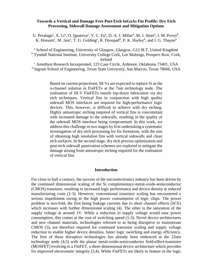
realisation of a highly vertical 10nm In0.53Ga0.47As fin with 16:1 aspect ratio as shown in
Fig. 5(a), perhaps the highest aspect ratio, smallest critical dimension fins that been
demonstrated to date in In0.53Ga0.47As. The details of this fin etch process are Cl2/CH4/H2 :
6/10/15sccm, coil/platen powers of 1000/75W, 2mTorr, 198V, 60°C, 45s. AFM was also
used to analyse the etched surface as shown in Fig. 5(b). The measured roughness of
0.456nm is indicative of device quality etching.
(a)
(b) (c)
(d) (e)
Ra = 0.284nm
Ra = 0.428nm Ra = 0.580nm
Ra = 0.516nm Ra = 0.417nm
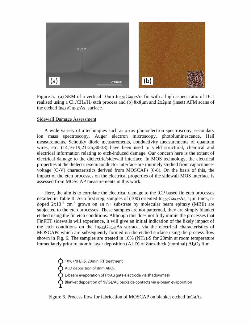
Figure 5. (a) SEM of a vertical 10nm In0.53Ga0.47As fin with a high aspect ratio of 16:1
realised using a Cl2/CH4/H2 etch process and (b) 8x8μm and 2x2μm (inset) AFM scans of
the etched In0.53Ga0.47As surface.
Sidewall Damage Assessment
A wide variety of a techniques such as x-ray photoelectron spectroscopy, secondary
ion mass spectroscopy, Auger electron microscopy, photoluminescence, Hall
measurements, Schottky diode measurements, conductivity measurements of quantum
wires, etc. (14,16-19,21-25,30-33) have been used to yield structural, chemical and
electrical information relating to etch-induced damage. Our concern here is the extent of
electrical damage to the dielectric/sidewall interface. In MOS technology, the electrical
properties at the dielectric/semiconductor interface are routinely studied from capacitance-
voltage (C-V) characteristics derived from MOSCAPs (6-8). On the basis of this, the
impact of the etch processes on the electrical properties of the sidewall MOS interface is
assessed from MOSCAP measurements in this work.
Here, the aim is to correlate the electrical damage to the ICP based fin etch processes
detailed in Table II. As a first step, samples of (100) oriented In0.53Ga0.47As, 1μm thick, n-
doped 2x1016 cm-3 grown on an n+ substrate by molecular beam epitaxy (MBE) are
subjected to the etch processes. These samples are not patterned, they are simply blanket
etched using the fin etch conditions. Although this does not fully mimic the processes that
FinFET sidewalls will experience, it will give an initial indication of the likely impact of
the etch conditions on the In0.53Ga0.47As surface, via the electrical characteristics of
MOSCAPs which are subsequently formed on the etched surface using the process flow
shown in Fig. 6. The samples are treated in 10% (NH4)2S for 20min at room temperature
immediately prior to atomic layer deposition (ALD) of 8nm-thick (nominal) Al2O3 film.
Figure 6. Process flow for fabrication of MOSCAP on blanket etched InGaAs.
(b)(a)
9.7nm

The gate electrode was defined via a shadow mask through which a Pt/Au contact was
electron-beam (e-beam) evaporated. A backside contact was formed by blanket e-beam
deposition of Ni/Ge/Au on the back of the samples. A MOSCAP was also fabricated on an
unetched sample to serve as a control in the study.
Shown in Fig. 7 are the room temperature multi-frequency (1kHz to 1MHz) C-V
characteristics of the unetched (control) sample and samples subject to the ICP etch
processes listed in Table II. The key electrical metrics derived from the C-V data of Fig. 7,
Figure 7. Multi-frequency, room temperature C-V characteristics of Au/Pt/Al2O3/n-
In0.53Ga0.47As MOSCAPs with the InGaAs sample (a) unetched (control) and etched for
the ICP conditions of (b) ICP-A , (c) ICP-B, (d) ICP-C and (e) ICP-D listed in Table II.

specifically the frequency dispersion in accumulation (ΔCacc), stretch-out of the C-V
curve (dC/dV), frequency dispersion in depletion (ΔmV) and hysteresis at 1MHz are
summarised in Table III. The definitions used for the extraction of these metrics can be
found in Ref. 34. Percentages, displayed in the table, are used to compare and quantify
the difference in metrics between an etched sample and a control sample. It is also worth
pointing out that a decrease in dC/dV is taken to mean an increase in the stretch-out.
TABLE III. Summary of metrics derived from the C-V responses of an unetched (control) sample and
samples etched under a variety of chlorine-based chemistries for the ICP conditions given in Table II.
MOSCAP Sample ΔCacc
(%/dec)
dC/dV x 10-7
(F/cm2.V)
ΔmV
(mV)
Hysteresis
(mV)
Control 2.17 9.15 100.7 126.0
ICP-A 2.28 (+5.1%) 8.38 (-8.4%) 105.2 (+4.5%) 117.4 (-6.8%)
ICP-B 2.29 (+5.5%) 8.27 (-9.6%) 70.7 (-29.8%) 84.8 (-32.7%)
ICP-C 2.33 (+7.4%) 8.27 (-9.6%) 139.2 (+38.2%) 105.8 (-16.0%)
ICP-D 2.48 (+14.3%) 5.31 (-42.0%) 169.1 (+67.9%) 190.3 (+51.0%)
Samples ICP-A, ICP-B and ICP-C, etched in Cl2/BCl3 based chemistries, presented
with a 5-7.5% increase in ΔCacc and a 8-10% increase in stretch-out. While ΔmV of samples
ICP-A and ICP-C are increased from that of the control sample, ICP-B in fact shows a
reduction. The hysteresis of all samples etched in a Cl2/BCl3 based process is smaller than
that of the control sample. In contrast, the metrics of sample ICP-D subject to the
Cl2/CH4/H2 etch process, which produced the best fin profile among all the etch recipes,
are found to be significantly degraded. It is notable that amongst the etched samples, ICP-
D demonstrates the largest degradation across all metrics.
In the depletion region, the C-V responses are comparable between the control sample
and samples etched in Cl2/BCl3 chemistry, including Ar (Figs. 7(a)-(d)). It is observed that
the C-V responses go through a peak in the gate bias range of 0V to -1.5V. Such a peak
response is a characteristic signature of interface defects (7,8,35). While peak responses
are also observed in the C-V curves of the sample etched in the Cl2/CH4/H2 chemistry, the
peaks are noticeably broader and higher in magnitude (Fig. 7(e)) which suggests an
increase in interface defect density (Dit) (35). The deterioration of the interface properties
of the sample etched in Cl2/CH4/H2 is also noted from the significant peak on the 1MHz
response. A similar feature is not present in the C-V response of the control sample or the
other etched samples. Equivalent parallel conductance (Gp/ω) can be used to provide an
indication of the relative differences in defect densities between the etched samples and the
control sample since there is direct correlation between Gp/ω and Dit (35). In Fig. 8, plots
of Gp/ω as a function of gate bias at a constant frequency of 1MHz and 100kHz are shown.
The peak magnitudes of Gp/ω is increased by a factor of 1.5-2 for samples etched in
Cl2/BCl3 based chemistries in comparison to the control sample. On the other hand, the
conductance peak of the sample etched in Cl2/CH4/H2 is a factor of 6.5-8.5 greater than the
control sample.

Figure 8. Gp/ω versus Vg of Au/Pt/Al2O3/n-In0.53Ga0.47As MOSCAPs, with the InGaAs
sample unetched (control) and etched using the ICP processes listed in Table II, at a
constant frequency of (a) 1MHz and (b) 100kHz.
Based on the aforementioned analysis it is clear the Cl2/CH4/H2 etch process induces
substantial damage to the In0.53Ga0.47As surface, despite the fact the surface roughness
obtained with this process is smaller than that of the Cl2/BCl3 based etch processes. It is
possible that methane and hydrogen present in the chemistry could be causing polymers
and/or carbon based contaminants to be deposited on the In0.53Ga0.47As surface, resulting
in the quality of the interface to be degraded. To elucidate such effects, TEM analysis was
undertaken. Shown in Fig. 9 are the cross-sectional TEM micrographs obtained from each
of the etched samples and the control sample following high-k dielectric and metal gate
deposition. These images confirm the thickness of the Al2O3, and correlate well with the
roughness measurements on each sample. From the TEM images, it is clear there is a sharp
transition from the In0.53Ga0.47As to the Al2O3 film with no obvious interlayer. Particularly,
for the Cl2/CH4/H2, there is no evidence of polymer deposition or the presence of carbon
on the In0.53Ga0.47As surface, to impact the electrical performance of the MOSCAPs. The
damage, therefore, is likely arising from the physical nature of the Cl2/CH4/H2 etch process.
The high anisotropy required for the realisation of near vertical fins with this etch process
is primarily provided by ion sputtering. The enhanced ion bombardment, however, also
induces more damage (18,21). The degree of damage is directly proportional to the ion
energy and inversely proportional to the ion mass (18). Looking back at Table II, the platen
power used with the Cl2/CH4/H2 etch process is noticeably higher compared to all the other
etch processes. The etch-induced damage can therefore be minimised by lowering the
platen power, which in turn reduces the ion energy.
Figure 9. Cross-sectional TEM of In0.53Ga0.47As samples subject to (a) no etching and
blanket etched using the ICP conditions of (b) ICP-A, (c) ICP-B, (d) ICP-C and (e) ICP-D
listed in Table II, prior to high-k and metal gate deposition.
Mitigation of Etch-induced Sidewall Damage
Dry Etch Process Optimization
As previously shown, the realisation of fins with near-90° sidewall verticality based on
a Cl2/CH4/H2 etch process comes at the cost of significant etch-induced damage. It was
highlighted that the high platen power of 75W used in the process is likely responsible for
this. In an effort to minimise the damage an ICP etch process based around a Cl2/CH4/H2/O2
chemistry is explored. The addition of O2 to the etch chemistry allows for the platen power
to be lowered, which should help with reducing the etch-induced damage without
compromising the fin sidewall profile.
Fins were etched in (100) oriented In0.53Ga0.47As(30nm)/In0.52Al0.48As samples
using the HSQ etch mask shown in Fig. 1, to obtain fin heights in the range of 40-50nm.
Two fin etch recipes were investigated, with the only difference being the platen
temperature. The process details are Cl2/CH4/H2/O2 : 6/10/15/0.5sccm, coil/platen powers
of 200/25W, 2mTorr, 113V, 5min. Shown in Fig. 10 are the SEM micrographs of fins
etched using the aforementioned process conditions at temperatures of 60°C and 120°C.
Highly vertical fin profiles are realised with both etch recipes. The fins etched at the higher
10 nm10 nm

temperature though show a more vertical sidewall profile, which closely resembles that of
the fins etched in the Cl2/CH4/H2 chemistry (Fig. 3(d)).
Figure 10. SEM of fins etched in In0.53Ga0.47As(30nm)/In0.52Al0.48As using a
Cl2/CH4/H2/O2 chemistry at temperatures of (a) 60°C and (b) 120°C for the process
conditions of Cl2/CH4/H2/O2 : 6/10/15/0.5sccm, coil/platen powers : 200/25W, 2mT, 113V,
5min.
To assess the damage associated with the Cl2/CH4/H2/O2 etch processes, MOSCAPs
were fabricated on samples of (100) oriented In0.53Ga0.47As, 1μm thick, n-doped 4x10¹⁷
cm-3 using the process flow illustrated in Fig. 6. A MOSCAP fabricated on an unetched
sample served as a control in the study. In Figs. 11(a)-(c) the room temperature multi-
frequency (1kHz to 1MHz) C-V characteristics of the control sample and samples etched
at the temperatures of 60°C and 120°C, denoted as A and B, are displayed. Etch-induced
damage is observed from the peak responses being broader and of higher magnitude in the
etched samples. It is further noted the fin etch process performed at the lower temperature
of 60°C gives rise to more damage as the peaks are observed to be broader and larger in
magnitude compared to sample A. From the plot of Gp/ω versus Vg (Fig. 11(d)),
conductance peaks of samples A and B are found to be 4.5x and 2.75x larger in relation to
the control sample as opposed to the larger factor of 8.5 reported earlier for the Cl2/CH4/H2
chemistry (Fig. 8(b)).
Table IV summarises the electrical metrics of the control and etched samples
determined from their respective C-V characteristics. Frequency dispersion in
accumulation and depletion along with stretch-out are observed to be less degraded for
sample B. While both the etched samples demonstrate a reduction in hysteresis, a larger
improvement is noted for sample B. These observations in conjunction with the
aforementioned Gp/ω analysis suggest the higher temperature etch process renders less
damage to the sidewall. Moreover, in contrast to the Cl2/CH4/H2 etch process there is a
marked improvement in the metrics of samples subject to the Cl2/CH4/H2/O2 etch process
designed Wfin = 100nm
111 8nm
nm
32
4
nm
85
4
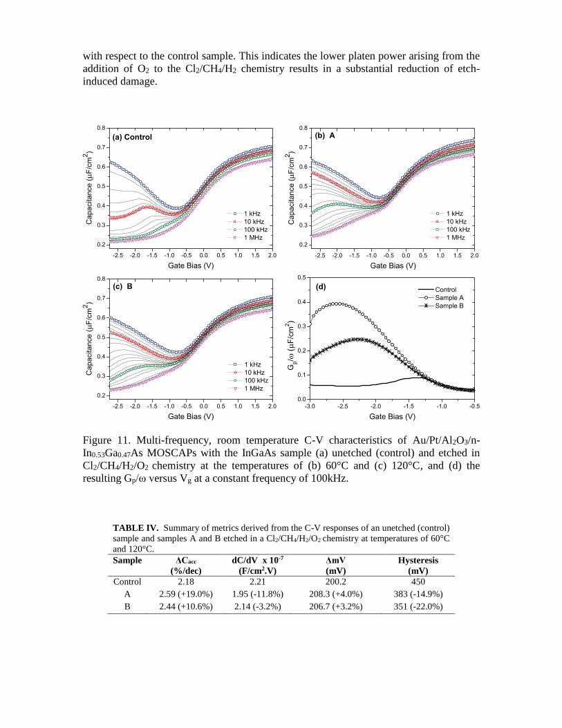
with respect to the control sample. This indicates the lower platen power arising from the
addition of O2 to the Cl2/CH4/H2 chemistry results in a substantial reduction of etch-
induced damage.
Figure 11. Multi-frequency, room temperature C-V characteristics of Au/Pt/Al2O3/n-
In0.53Ga0.47As MOSCAPs with the InGaAs sample (a) unetched (control) and etched in
Cl2/CH4/H2/O2 chemistry at the temperatures of (b) 60°C and (c) 120°C, and (d) the
resulting Gp/ω versus Vg at a constant frequency of 100kHz.
TABLE IV. Summary of metrics derived from the C-V responses of an unetched (control)
sample and samples A and B etched in a Cl2/CH4/H2/O2 chemistry at temperatures of 60°C
and 120°C.
Sample ΔCacc
(%/dec)
dC/dV x 10-7
(F/cm2.V)
ΔmV
(mV)
Hysteresis
(mV)
Control 2.18 2.21 200.2 450
A 2.59 (+19.0%) 1.95 (-11.8%) 208.3 (+4.0%) 383 (-14.9%)
B 2.44 (+10.6%) 2.14 (-3.2%) 206.7 (+3.2%) 351 (-22.0%)
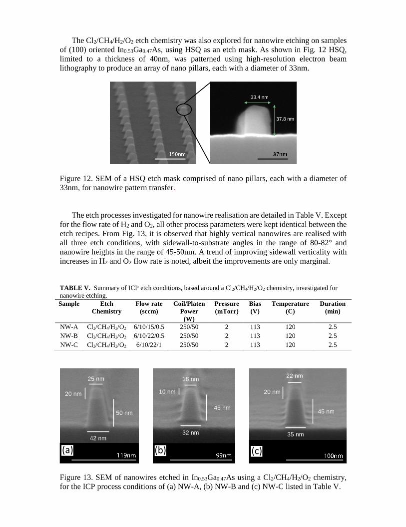
The Cl2/CH4/H2/O2 etch chemistry was also explored for nanowire etching on samples
of (100) oriented In0.53Ga0.47As, using HSQ as an etch mask. As shown in Fig. 12 HSQ,
limited to a thickness of 40nm, was patterned using high-resolution electron beam
lithography to produce an array of nano pillars, each with a diameter of 33nm.
Figure 12. SEM of a HSQ etch mask comprised of nano pillars, each with a diameter of
33nm, for nanowire pattern transfer.
The etch processes investigated for nanowire realisation are detailed in Table V. Except
for the flow rate of H2 and O2, all other process parameters were kept identical between the
etch recipes. From Fig. 13, it is observed that highly vertical nanowires are realised with
all three etch conditions, with sidewall-to-substrate angles in the range of 80-82° and
nanowire heights in the range of 45-50nm. A trend of improving sidewall verticality with
increases in H2 and O2 flow rate is noted, albeit the improvements are only marginal.
TABLE V. Summary of ICP etch conditions, based around a Cl2/CH4/H2/O2 chemistry, investigated for
nanowire etching. Sample Etch
Chemistry
Flow rate
(sccm)
Coil/Platen
Power
(W)
Pressure
(mTorr)
Bias
(V)
Temperature
(C)
Duration
(min)
NW-A Cl2/CH4/H2/O2 6/10/15/0.5 250/50 2 113 120 2.5
NW-B Cl2/CH4/H2/O2 6/10/22/0.5 250/50 2 113 120 2.5
NW-C Cl2/CH4/H2/O2 6/10/22/1 250/50 2 113 120 2.5
Figure 13. SEM of nanowires etched in In0.53Ga0.47As using a Cl2/CH4/H2/O2 chemistry,
for the ICP process conditions of (a) NW-A, (b) NW-B and (c) NW-C listed in Table V.
33.4 nm
37.8 nm
25 nm
50 nm
42 nm
20 nm
(a)
45 nm
18 nm
32 nm
10 nm
45 nm
22 nm
35 nm
20 nm
(b) (c)
Post-etch Sidewall Passivation Schemes
Hydrogenation. The preparation of clean, well-ordered, stoichiometric and atomically
smooth surfaces are of importance in semiconductor processing. Atomic hydrogen has
been demonstrated to be an effective surface preparation technique due to its ability to
remove carbon-containing contaminants and native oxides (36-38). The lower
temperatures required of atomic hydrogen cleaning alleviates the problems of group V
desorption and surface roughening typically associated with high temperature thermal
cleaning of substrates prior to epitaxial growth (36-38). A notable obstacle in III-V MOS
technology is the presence of a large density of defects at the dielectric/semiconductor
interface. This can result in the Fermi level to be pinned, thereby limiting logic
performance. Native oxides present on III-V surfaces have been proposed as one cause of
Fermi level pinning (39). The reduction and/or removal of these oxides by means of atomic
hydrogen cleaning have been shown to unpin the Fermi level (40,41) and reduce interface
defect density (42). Another key feature of atomic hydrogen is its ability to passivate native
defects within the semiconductor (23,30,43). This attribute has also been exploited in GaN
and GaAs to recover damage arising from dry etch processing through the passivation of
etch-induced defects (44,45). This motivates an investigation of atomic hydrogen as a post-
etch treatment for the alleviation of etch-induced damage in In0.53Ga0.47As.
Atomic hydrogen is often introduced into semiconductors through controlled methods
such as direct implantation (43), exposure to hydrogen plasmas (36,38,42-44) and from
thermal cracking of molecular hydrogen (36-38,40,41). The first two methods, though,
carry the risk of physical and electronic damage to the near surface regions of the
semiconductor due to the presence of energetic ions (36,43). Here, we employ a photon-
assisted hydrogenation process (46) developed by Amethyst Research Incorporated to
investigate mitigation of damage induced by the fin etch process. This process involves the
irradiation of samples with an ultraviolet (UV) light source in a hydrogen ambient. The
extent of hydrogen incorporation is controlled and optimized by temperature, exposure
time and pressure.
To investigate the effects of hydrogenation, four MOSCAPs were fabricated on
samples of (100) oriented In0.53Ga0.47As, 1μm thick, n-doped 4x1017 cm-3 using the process
flow of Fig. 6. For a controlled study, one sample did not see any etch process prior to
MOSCAP fabrication. The remaining three samples were subject to a fin etch process. The
process details are Cl2/CH4/H2 : 6/10/15sccm, coil/platen powers of 500/75W, 2mTorr,
182V, 60°C, 60s. A MOSCAP was directly fabricated on one of the etched samples. The
remaining two samples underwent hydrogenation at different stages of the process flow for
MOSCAP fabrication shown in Fig. 6. One sample underwent hydrogenation after the etch
(post-etch hydrogenation) while the other was hydrogenated after Al2O3 deposition (post
ALD high-k hydrogenation). Hydrogenation was carried out at a temperature of 325°C for
30min, with the pressure set at 1mbar.
Multi-frequency (100Hz to 1MHz) C-V characteristics acquired at room temperature
from the four samples are shown in Fig. 14. The electrical metrics extracted from the C-V
curves of each sample are also detailed in Table VI. Although the post-etch hydrogenated
sample shows an improvement across all metrics from the etched sample, the obtained

enhancement is marginal. In contrast, a significant reduction in stretch-out and depletion
dispersion is obtained for the post high-k hydrogenated sample. These results suggest that
hydrogenation done post high-k is more effective in alleviating etch-induced damage. The
large conductance peak associated with the etched samples at a constant frequency of
1MHz shown in Fig. 15 is reduced substantially in magnitude after post-etch hydrogenation.
A larger reduction in the peak value is obtained by hydrogenating the etched sample post
high-k as opposed to post-etch.
Figure 14. Multi-frequency, room temperature C-V characteristics of Au/Pt/Al2O3/n-
In0.53Ga0.47As MOSCAPs with the InGaAs sample (a) unetched (control), (b) only etched,
etched and subjected to the treatments of (c) post-etch hydrogenation and (d) post ALD
high-k hydrogenation.
TABLE VI. Summary of metrics derived from the C-V responses of samples investigated in the
hydrogenation experiment.
Sample ΔCacc
(%/dec)
dC/dV x 10-7
(F/cm2.V)
ΔmV
(mV)
Control 2.84 2.49 322
Fin etch 3.82 (+34.5%) 1.63 (-34.5%) 605 (+87.9%)
Post-etch hydrogenation 3.72 (+31.0%) 1.81 (-27.3%) 595 (+84.8%)
Post ALD high-k hydrogenation 3.68 (+29.6%) 2.31 (-7.2%) 334 (+3.7%)
Figure 15. Gp/ω versus Vg of Au/Pt/Al2O3/n-In0.53Ga0.47As MOSCAPs investigated in the
hydrogenation experiment, at a constant frequency of 1MHz.
Digital Etch In standard wet etching, semiconductors are immersed into a solution
comprising an oxidising agent and an etching agent. Etching proceeds through the
simultaneous process of surface oxidation and oxide etching. As a result, the depth of
material etched is dictated by the length of time the semiconductor is exposed to the etchant.
Digital etch, on the other hand, separates the two processes of oxidation and oxide removal.
Etching is then achieved through the sequential application of the oxidant and etchant to
ensure the chemical reactions associated with each process are independent of each other.
(47, 48) Due to the self-limiting nature of the oxidation process, the depth of material
removed is only dependent on the number of etch cycles and not on the etch time (48). The
main benefit of digital etch compared to standard wet etching is the fact that etching can
be performed in a controlled manner. This property of digital etch can be exploited in two
ways, the first being for the removal of dry etch damaged semiconductor layers (27).
Digital etch also offers a route for ultimate fin/nanowire scaling (49).
In this work, we assess the impact of a digital etch clean for the mitigation of damage
induced by fin etch processing. This is investigated on a sample of (100) oriented
In0.53Ga0.47As, 1μm thick, n-doped 4x1017 cm-3 blanket etched using the 120°C,
Cl2/CH4/H2/O2 etch process. The details of the etch are Cl2/CH4/H2/O2 : 6/10/15/0.5sccm,
coil/platen powers of 200/25W, 2mTorr, 113V, 120°C, 5min. The etched surface is then
subjected to three cycles of the digital etch clean. Each cycle is a two-step process
comprising a self-limiting O2 plasma oxidation in a RIE tool followed by a 10s rinse in
diluted H2SO4 for oxide removal. Plasma oxidation was carried out under the conditions
of 50sccm, 50mTorr, 52V, 22°C, 3s. We estimate that one cleaning cycle etches 1nm of
the In0.53Ga0.47As material. The process flow of Fig. 6 is adopted for the realisation of
MOSCAPs on this sample.
The C-V data acquired on the cleaned sample is shown in Fig. 16(a). To elucidate the
impact of the digital etch clean, a comparison in C-V characteristics is drawn between the
cleaned sample, a control sample (Fig. 11(a)) and a sample blanket etched under the same
fin etch conditions (Fig. 11(c)). From this comparison, it is evident that the C-V
characteristics of the cleaned sample is significantly improved, with all electrical metrics

showing improvements, over the etched sample. Additionally, the conductance peak of the
etched sample is reduced by a factor of three in value after being subjected to the digital
etch clean. This highlights the benefit of the digital etch clean for mitigating damage
induced by fin etch processes. It is also noteworthy that the C-V data between the control
sample and the cleaned sample is comparable. This is an important observation as it
suggests the etch-induced damage has been completely recovered via the digital etch clean,
resulting in the restoration of the Al2O3/In0.53Ga0.47As interface to its original state prior to
etching. This also implies the damage induced by 120°C, Cl2/CH4/H2/O2 etch process only
extends to the near surface region, up to a depth of about 3nm from the surface based on
the etch rate (1nm/cycle) and the number of cleaning cycles used.
Figure 16. (a) Multi-frequency, room temperature C-V characteristics of a Au/Pt/Al2O3/n-
In0.53Ga0.47As MOSCAP with the InGaAs sample subjected to the 120°C, Cl2/CH4/H2/O2
based fin etch process followed by the digital etch clean and (b) Gp/ω versus Vg of
Au/Pt/Al2O3/n-In0.53Ga0.47As MOSCAPs with the InGaAs sample subjected to no etch
(control), the fin etch process only and the fin etch process followed by the digital etch
clean, at a constant frequency of 100kHz.
Mitigation of fin etch damage by means of the digital etch clean was also examined
on etched (110) oriented In0.53Ga0.47As. For this investigation, 200nm thick n-type (110)
In0.53Ga0.47As layer doped at 4x1017 cm-3 was grown by molecular beam epitaxy (MBE) on
(110) n+-InP substrate. Of the three samples fabricated from (110) In0.53Ga0.47As for
electrical evaluation, one served as control (unetched) while the others were blanket etched.
The digital etch clean was then carried out on one of the etched samples. The conditions of
the fin etch process, used for blanket etching, and the digital etch clean are identical to that
used in the earlier study reporting on the effectiveness of digital etch clean on etched (100)
In0.53Ga0.47As. The fabrication of MOSCAPs was based on the process flow of Fig. 6.
The room temperature CV data of the unetched sample (control), the sample
subjected to the fin etch process (etched), and for the sample subjected to the fin etch
process followed by the digital etch clean (cleaned) are compared in Fig. 17. It is clear
that etched sample has significantly degraded C-V response, evidenced by a stretch-out in
the characteristics and the fact that the 100kHz and 1MHz capacitance does not reach the
theoretical minimum capacitance of 2.5x10⁻⁷ F/cm2. In contrast, the cleaned sample
appears to have regained many of the characteristics of the control sample, and indeed the

peak in depletion around -1V, evident in both the 10kHz and 100kHz data, is suppressed
in the cleaned sample. This implies recovery of damage in etched (110) In0.53Ga0.47As,
similar to the finding noted for post-etch cleaned (100) In0.53Ga0.47As.
Figure 17. Multi-frequency, room temperature C-V characteristics of a Au/Pt/Al2O3/n-
(110) In0.53Ga0.47As MOSCAP with the InGaAs sample (a) unetched (control), (b) subject
to the fin etch process (etched) and (c) subjected to the fin etch process followed by the
digital etch clean (cleaned).
Conclusion
The introduction of III-V channels into CMOS, currently aimed at the 7nm technology
node, would require top-down patterning of III-V fins. The realisation of fins with a vertical
profile and a high quality sidewall MOS interface, however, is a challenging prospect.
Reason being, highly anisotropic etching required of vertical fin profiles is more damaging
to the sidewall. To tackle the conflict between anisotropy and damage, inherent to dry etch
processing, we adopted a two-tier approach to realise vertical In0.53Ga0.47As fins with
minimum etch damage. In the first tier, we focussed on developing dry etch processes
capable of producing high resolution fins with vertical sidewalls and clean etch surfaces.
Fin etching was investigated for a variety of chlorine-based chemistries using either a RIE
or an ICP process. A fin profile within 3˚ of vertical was obtained with the ICP process
based around a Cl2/CH4/H2 chemistry. Vertical 10nm fins with 16:1 aspect ratio, perhaps
the highest aspect ratio, smallest critical dimension fins to date in In0.53Ga0.47As, was also
achieved. The process, however, severely degraded the electrical characteristics of
MOSCAPs formed on a (100) In0.53Ga0.47As surface subjected to the etch which indicated
substantial etch-induced damage. The aim in the second tier was then to mitigate the
damage. The modification of the Cl2/CH4/H2 chemistry to include O2 resulted in the
substantial reduction of etch-induced damage, due to the lowering of the platen power,
without compromising on the fin profile. Two post-etch sidewall passivation schemes were
also examined for damage mitigation. The first was a photon-assisted hydrogenation
process, applied post-etch or post high-k. The electrical performance of MOSCAPs formed
on a (100) In0.53Ga0.47As surface subjected to the Cl2/CH4/H2 etch indicated a larger
reduction in etch damage for hydrogenation done post high-k. In the second approach, a
digital etch clean, comprising of a multi-cycle O2 plasma oxidation then oxide removal in
H2SO4, was investigated as a post-etch treatment. The electrical characteristics of
MOSCAPs formed on (100) In0.53Ga0.47As and (110) In0.53Ga0.47As surfaces subjected to
the Cl2/CH4/H2/O2 etch revealed a complete recovery of etch damage. The demonstration
of high resolution (10 nm), near-vertical (~87°) In0.53Ga0.47As fins and the ability to realise

damage-free sidewalls are of significance for the realisation of high-performance III-V
FinFETs.
Acknowledgments
The authors acknowledge support from the Semiconductor Research Corporation (Task
ID 2188.002) and technical support from the James Watt Nanofabrication Centre (JWNC)
University of Glasgow.
References
1. J. A. del Alamo, Nature, 479, 317 (2011).
2. H. Iwai, Microelectron. Eng., 86, 1520 (2009).
3. H. Riel, L. -E. Wernersson, M. Hong, J. A. del Alamo, MRS Bulletin, 39, 668 (2014).
4. I. Ferain, C. A. Colinge, J. -P. Colinge, Nature, 479, 310 (2011).
5. C. C. Wu, D. W. Lin, A. Keshavarzi, C. H. Huang, C. T. Chan, C. H. Tseng, C. L.
Chen, C. Y. Hsieh, K. Y. Wong, M. L. Cheng, T. H. Li, Y. C. Lin, L. Y. Yang, C.
P. Lin, C. S. Hou, H. C. Lin, J. L. Yang, K. F. Yu, M. J. Chen, T. H. Hsieh, Y. C.
Peng, C. H. Chou, C. J. Lee, C. W. Huang, C. Y. Lu, F. K. Yang, H. K. Chen, L.
W. Weng, P. C. Yen, S. H. Wang, S. W. Chang, S.W. Chuang, T. C. Gan, T. L. Wu,
T. Y. Lee, W. S. Huang, Y. J. Huang, Y. W. Tseng, C. M. Wu, E. Ou-Yang, K. Y.
Hsu, L. T. Lin, S. B. Wang, T. M. Kwok, C. C. Su, C. H. Tsai, M. J. Huang, H. M.
Lin, A. S. Chang, S. H. Liao, L. S. Chen, J. H. Chen, P. S. Lim, X. F. Yu, S. Y. Ku,
Y. B. Lee, P. C. Hsieh, P. W. Wang, Y. H. Chiu, S. S. Lin, H. J. Tao, M. Cao, Y. J.
Mii, IEEE IEDM Tech. Dig., 2711 (2010).
6. S. Oktyabrsky, M. Yakimov, V. Tokranov, R. Kambhampati, H,. Bakhru, S.
Koveshnikov, W. Tsai, F. Zhu, J. Lee, International Journal of High Speed
Electronics and Systems, 18, 761 (2008).
7. P. K. Hurley, E. O'Connor, V. Djara, S. Monaghan, I. M. Povey, R. D. Long, B.
Sheehan, J. Lin, P. C. McIntyre, B. Brennan, R. M. Wallace, M. E. Pemble, K.
Cherkaoui, IEEE Trans. Device Mater. Rel., 13, 429 (2013).
8. V. Chobpattana, E. Mikheev, J. Y. Zhang, T. E. Mates, S. Stemmer, J. Appl. Phys.,
116, 124104 (2014).
9. R. Oxland, S. W. Chang, X. Li, S. W. Wang, G. Radhakrishnan, W. Priyantha, M.
J. H. van Dal, C. H. Hsieh, G. Vellianitis, G. Doornbos, K. Bhuwalka, B. Duriez, I.
Thayne, R. Droopad, M. Passlack, C. H. Diaz, Y. C. Sun, IEEE Elec. Dev. Lett.,
33, 501 (2012).
10. R. J. W. Hill, C. Park, J. Barnett, J. Price, J. Huang, N. Goel, W. -Y. Loh, J. Oh, C.
E. Smith, P. Kirsch, P. Majhi, R. Jammy, IEEE IEDM Tech. Dig., 621 (2010).
11. S. Lee, V. Chobpattana, C. -Y. Huang, B. J. Thibeault, W. Mitchell, S. Stemmer,
A. C. Gossard, M. J. W. Rodwell, VLSI Technology Tech. Dig., 54 (2014).
12. C. Y. Huang, S. Lee, V. Chobpattana, S. Stemmer, A. C. Gossard, B. Thibeault, W.
Mitchell, M. Rodwell, IEEE IEDM Tech. Dig., 586 (2014).
13. S. W. Chang, X. Li, R. Oxland, S. W. Wang, C. H. Wang, R. Contreras-Guerrero,
K. K. Bhuwalka, G. Doornbos, T. Vasen, M. C. Holland, G. Vellianitis, M. J. H.
van Dal, B. Duriez, M. Edirisooriya, J. S. Rojas-Ramirez, P. Ramvall, S. Thoms,

U. Peralagu, C. H. Hsieh, Y. S. Chang, K. M. Yin, E. Lind, L. -E. Wernersson, R.
Droopad, I. Thayne, M. Passlack, C. H. Diaz, IEEE IEDM Tech. Dig., 417 (2013).
14. S. J. Pearton, U. K. Chakrabarti, W. S. Hobson and A. P. Perley, J. Electrochern.
Soc., 137, 3188 (1990).
15. J. W. Lee, E. S. Lambers, C. R. Abernathy, S. J. Pearton, R. J. Shul, F. Ren, W. S.
Hobson, C. Constantine, Mater. Sci. Semicond. Process., 1, 65 (1998).
16. T Maeda, J. W. Lee, R. J. Shul, J. Han, J. Hong, E. S. Lambers, S. J. Pearton, C. R.
Abernathy, W. S. Hobson, Appl. Surf. Sci., 143, 174 (1999).
17. T Maeda, J. W. Lee, R. J. Shul, J. Han, J. Hong, E. S. Lambers, S. J. Pearton, C. R.
Abernathy, W. S. Hobson, Appl. Surf. Sci., 143, 183 (1999).
18. S. J. Pearton, F. Ren, T. R. Fullowan, A. Katz, W. S. Hobson, U. K. Chakrabarti,
C. R. Abernathy, Mater. Chem. Phys, 32, 215 (1992).
19. C. D. Wilkinson and M. Rahman, Philos Trans A Math Phys Eng Sci., 362, 125
(2004).
20. F. Karouta, J. Phys. D: Appl. Phys., 47, 233501 (2014).
21. S. J. Fonash, J. Electrochem. Soc., 137, 3885 (1990).
22. G. Franz, J. Vac. Sci. Technol. A, 19, 762 (2001).
23. T. R. Hayes, W. C. Dautremont-Smith, H. J. Luftman, J. W. Lee, Appl. Phys. Lett.,
55, 56 (1989).
24. R. van Roijen, M. B. M. Kemp, C. W. Bulle-Lieuwma, L. J. van Ijzerdoorn, T. L.
Thijssen, J. Appl. Phys., 70, 3983 (1991).
25. S. J. Pearton, U. K. Chakrabarti, F. A. Baiochi, Appl. Phys. Lett., 55,1633 (1989).
26. A. Dixit, T. B. Hook, J. B. Johnson, E. J. Nowak and K. V. Murali, in Physics of
Semiconductor Devices, V. K. Jain and A. Verma, Editors, p. 5, Springer-Verlag,
New York (2014).
27. X. Zhao, J. A. del Alamo, IEEE Elec. Dev. Lett., 35, 521 (2014).
28. M. Volatier, D. Duchesne, R. Morandotti, R. Arès, V. Aimez, Nanotechnology, 21,
134014 (2010).
29. L. Gatilova, S. Bouchoule, S. Guilet, P. Chabert, J. Vac. Sci. Technol. A, 27, 262
(2009).
30. L. Goubert, R. L. Van Meirhaeghe, P. Clauws, F. Cardon, P. Van Daele, J. Appl.
Phys., 82, 1696 (1997).
31. H. C. Neitzert, R. Fang, M. Kunst, N. Layadi, J. Vac. Sci. Technol. B, 18, 2803
(2000).
32. T. R. Hayes, U. K. Chakrabarti, F. A. Baiocchi, A. B. Emerson, H. S. Luftman, W.
C. Dautremon-Smith, J. Appl. Phys., 68, 785 (1990).
33. A. R. Long, M. Rahman, I. K. MacDonald, M. Kinsler, S. P. Beaumont, C. D. W.
Wilkinson, C. R. Stanley, Semicond. Sci. Technol., 8, 39 (1993).
34. U. Peralagu, I. M. Povey, P. Carolan, J. Lin, R. Contreras-Guerrero, R. Droopad, P.
K. Hurley and I. G. Thayne, Appl. Phys. Lett., 105, 162907 (2014).
35. E. O’Connor, B. Brennan, V. Djara, K. Cherkaoui, S. Monaghan, S. B. Newcomb,
R. Contreras, M. Milojevic, G. Hughes, M. E. Pemble, R. M. Wallace, and P. K.
Hurley, J. of Appl. Phys., 109, 024101 (2011).
36. G. R. Bell, N. S. Kaijaks, R. J. Dixon, C. F. McConville, Surf. Sci., 401, 125 (1998).
37. A. Khatiri, J. M. Ripalda, T. J. Krzyzewski, G. R. Bell, C. F. McConville, T. S.
Jones, Surf. Sci., 548, L1 (2004).
38. T. Kikawa, I. Ochiai, S. Takatani, Surf. Sci., 316, 238 (1994).
39. H. Hasegawa, M. Akazawa, A. Domanowska, B. Adamowicz, Appl. Surf. Sci., 256,
5698 (2010).

40. W. Melitz, J. Shen, T. Kent, A. C. Kummel and R. Droopad, J. Appl. Phys., 110,
013713 (2011).
41. J. Szuber, Vacuum, 55, 209 (2000).
42. A. D. Carter, W. J. Mitchell, B. J. Thibeault, J. J. M. Law, M. J. W. Rodwell, Appl.
Phys. Express, 4, 091102 (2011).
43. S. J. Pearton, J. W. Corbett, T. S. Shi, Appl. Phys. A, 43, 153 (1987).
44. B. -S. Yoo, S. -J. Park, K. -H. Park, J. Vac. Sci. Technol. A, 13, 931 (1995).
45. S. Chen, Y. Lu, R. Kometani, K. Ishikawa, H. Kondo, Y. Tokuda, M. Sekine, M.
Hori, AIP Advances, 2, 022149 (2012).
46. H1. T. D. Golding and R. P. Hellmer 2008, Photon-assisted hydrogenation process,
US Patent 0268658.
47. X. Cao, I. Thayne, Microelectron. Eng., 67, 333 (2003).
48. G. C. DeSalvo, C. A. Bozada, J. L. Ebel, D. C. Look, J. P. Barrette, C. L. A. Cerny,
R. W. Dettmer, J. K. Gillespie, C. K. Havasy, T. J. Jenkins, K. Nakano, C. I.
Pettiford, T. K. Quach, J. S. Sewell, G. David Via, J. Electrochem. Soc., 143, 3652
(1996).
49. J. Lin, X. Zhao, D. A. Antoniadis, J. A. del Alamo, IEEE Elec. Dev. Lett., 35, 440
(2014).


![ars.els-cdn.com · Web view(((((((((((light exposure[Title/Abstract]) OR artificial light at night[Title/Abstract]) OR artificial light-at-night[Title/Abstract]) OR night time light[Title](https://img.pdfslide.us/doc/110x75/5f3af4cdf401aa53436ccbca/arsels-cdncom-web-view-light-exposuretitleabstract-or-artificial.jpg)


![[Topic Letter / Abstract Number] [Title of your Abstract]](https://img.pdfslide.us/doc/110x75/56812dcf550346895d930f75/topic-letter-abstract-number-title-of-your-abstract.jpg)

