Embed Size (px)
Citation preview
Tips and Tricks for Successful Power Designs Part 1: EMI/EMC Part 2: Optimizing Efficiency
1
2
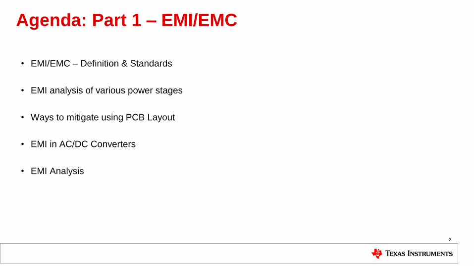
Agenda: Part 1 – EMI/EMC
• EMI/EMC – Definition & Standards
• EMI analysis of various power stages
• Ways to mitigate using PCB Layout
• EMI in AC/DC Converters
• EMI Analysis
3
Key Learnings
• EMI and the standards
• Root cause of EMI created by ALL Switched Mode Power Supplies
• PCB and Ground Techniques to Mitigate EMI
• Noise Sources in a Real Schematic
• Measurement of EMI
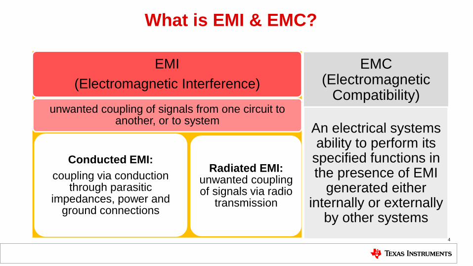
What is EMI & EMC?
4
EMI
(Electromagnetic Interference)
unwanted coupling of signals from one circuit to another, or to system
Conducted EMI:
coupling via conduction through parasitic
impedances, power and ground connections
Radiated EMI: unwanted coupling of signals via radio
transmission
EMC (Electromagnetic
Compatibility)
An electrical systems ability to perform its
specified functions in the presence of EMI
generated either internally or externally
by other systems
5
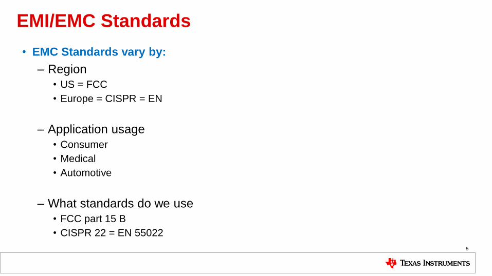
EMI/EMC Standards
• EMC Standards vary by:
– Region
• US = FCC
• Europe = CISPR = EN
– Application usage
• Consumer
• Medical
• Automotive
– What standards do we use
• FCC part 15 B
• CISPR 22 = EN 55022
6
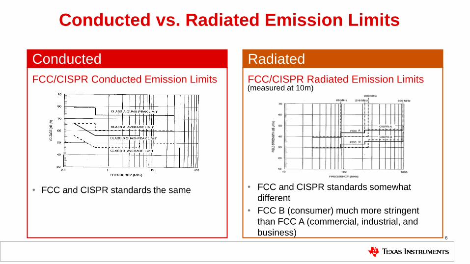
Conducted vs. Radiated Emission Limits
Conducted Radiated
FCC/CISPR Conducted Emission Limits
• FCC and CISPR standards somewhat
different
• FCC B (consumer) much more stringent
than FCC A (commercial, industrial, and
business)
• FCC and CISPR standards the same
FCC/CISPR Radiated Emission Limits (measured at 10m)
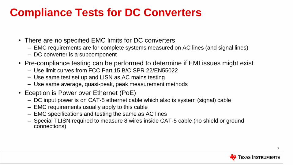
Compliance Tests for DC Converters
7
• There are no specified EMC limits for DC converters – EMC requirements are for complete systems measured on AC lines (and signal lines)
– DC converter is a subcomponent
• Pre-compliance testing can be performed to determine if EMI issues might exist – Use limit curves from FCC Part 15 B/CISPR 22/EN55022
– Use same test set up and LISN as AC mains testing
– Use same average, quasi-peak, peak measurement methods
• Eception is Power over Ethernet (PoE) – DC input power is on CAT-5 ethernet cable which also is system (signal) cable
– EMC requirements usually apply to this cable
– EMC specifications and testing the same as AC lines
– Special TLISN required to measure 8 wires inside CAT-5 cable (no shield or ground connections)
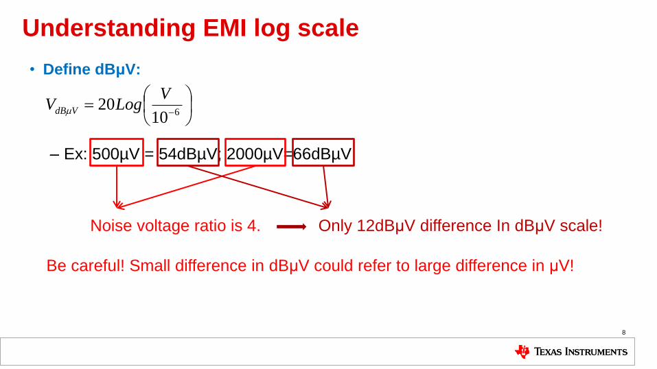
• Define dBμV:
– Ex: 500µV = 54dBµV; 2000µV=66dBµV
8
Understanding EMI log scale
61020
VLogV VdB
Noise voltage ratio is 4. Only 12dBμV difference In dBμV scale!
Be careful! Small difference in dBμV could refer to large difference in μV!
9
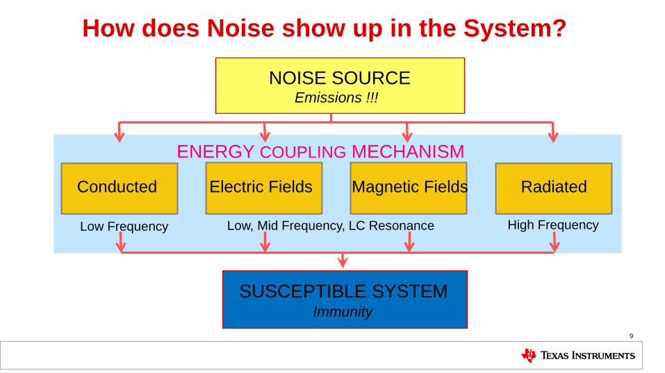
How does Noise show up in the System?
NOISE SOURCE Emissions !!!
SUSCEPTIBLE SYSTEM Immunity
ENERGY COUPLING MECHANISM
Conducted Electric Fields Magnetic Fields Radiated
Low Frequency Low, Mid Frequency, LC Resonance High Frequency
10
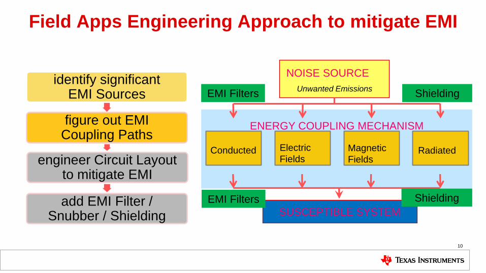
Field Apps Engineering Approach to mitigate EMI
SUSCEPTIBLE SYSTEM
NOISE SOURCE
Unwanted Emissions
ENERGY COUPLING MECHANISM
Conducted Electric
Fields Magnetic
Fields Radiated
identify significant EMI Sources
figure out EMI Coupling Paths
engineer Circuit Layout to mitigate EMI
EMI Filters Shielding
Shielding add EMI Filter / Snubber / Shielding
EMI Filters
11
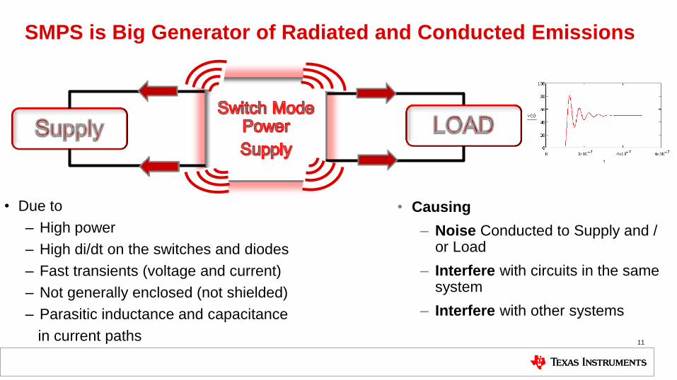
SMPS is Big Generator of Radiated and Conducted Emissions
• Due to
– High power
– High di/dt on the switches and diodes
– Fast transients (voltage and current)
– Not generally enclosed (not shielded)
– Parasitic inductance and capacitance
in current paths
• Causing
– Noise Conducted to Supply and / or Load
– Interfere with circuits in the same system
– Interfere with other systems
12
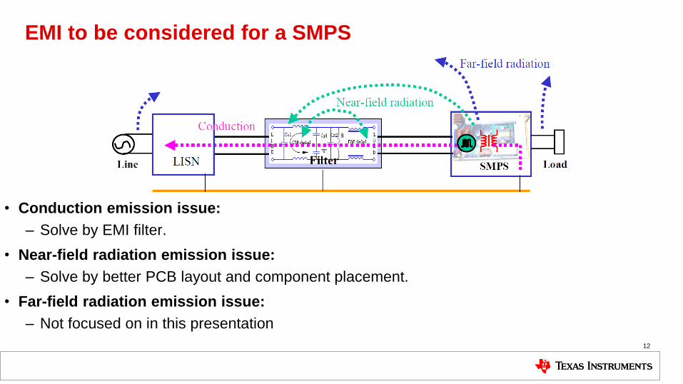
EMI to be considered for a SMPS
• Conduction emission issue:
– Solve by EMI filter.
• Near-field radiation emission issue:
– Solve by better PCB layout and component placement.
• Far-field radiation emission issue:
– Not focused on in this presentation
13
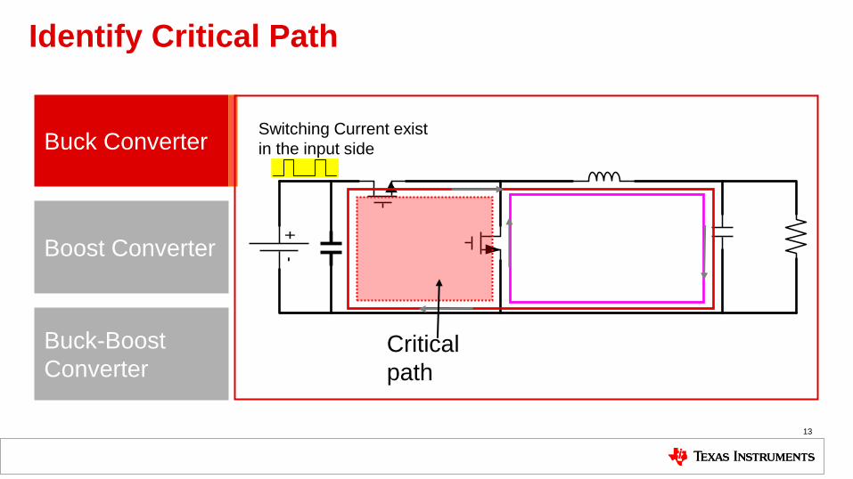
-+
Identify Critical Path
Buck Converter
Boost Converter
Buck-Boost
Converter Critical
path
Switching Current exist
in the input side
14
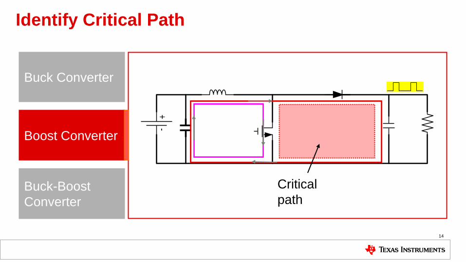
-+
Identify Critical Path
Buck Converter
Boost Converter
Buck-Boost
Converter
Critical
path
15
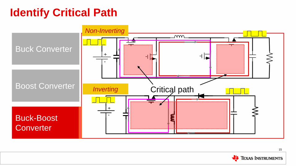
-+
Identify Critical Path
Buck Converter
Boost Converter
Buck-Boost
Converter
-+
Critical path
Non-Inverting
Inverting
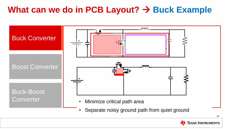
What can we do in PCB Layout? Buck Example
-+Buck Converter
Boost Converter
Buck-Boost
Converter
-+
• Minimize critical path area
• Separate noisy ground path from quiet ground 16
17 17
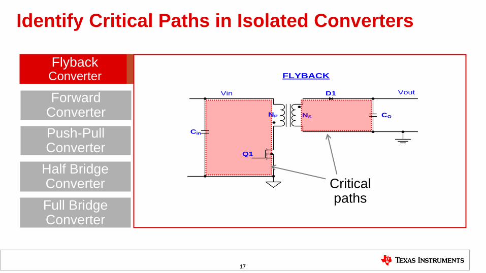
Identify Critical Paths in Isolated Converters
Flyback Converter
Forward Converter
Critical paths
Push-Pull Converter
Half Bridge Converter
Full Bridge Converter
FLYBACK
D1
CO NS
Q1
Vin Vout
NP
Cin
18 18
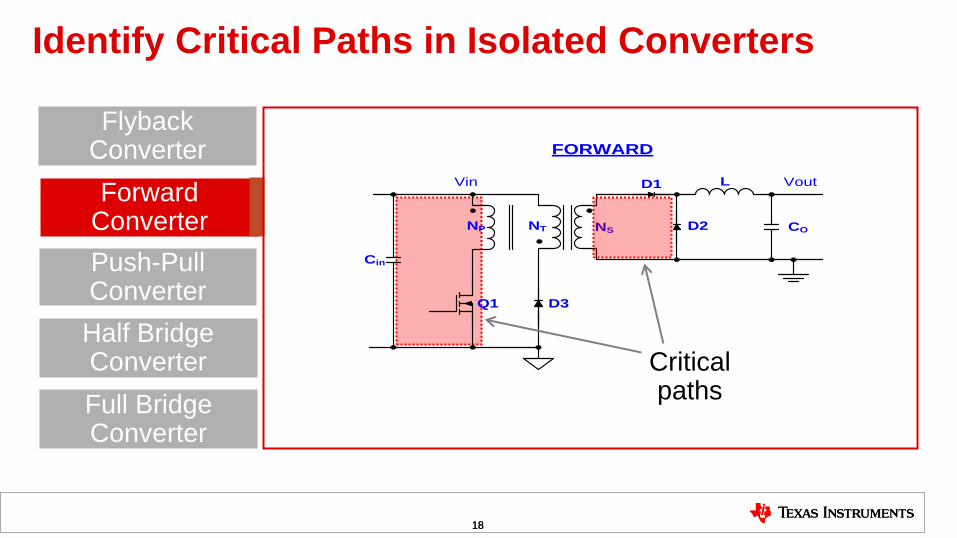
Identify Critical Paths in Isolated Converters
Flyback Converter
Forward Converter
Critical paths
Push-Pull Converter
Half Bridge Converter
Full Bridge Converter
FORWARD
D1
CO NS
Q1
D2
L
D3
Vin Vout
NT NP
Cin
19 19
Identify Critical Paths in Isolated Converters
Flyback Converter
Forward Converter
Critical paths
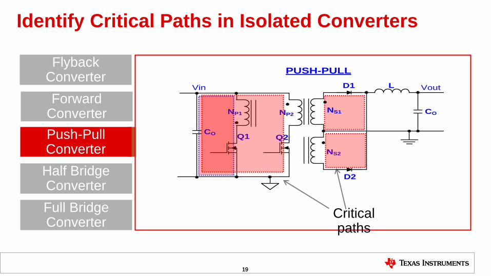
Push-Pull Converter
Half Bridge Converter
Full Bridge Converter
PUSH-PULL
L D1
NS1 NP1
Q2 Q1
CO
D2
NP2
NS2
Vin Vout
CO
20 20
Identify Critical Paths in Isolated Converters
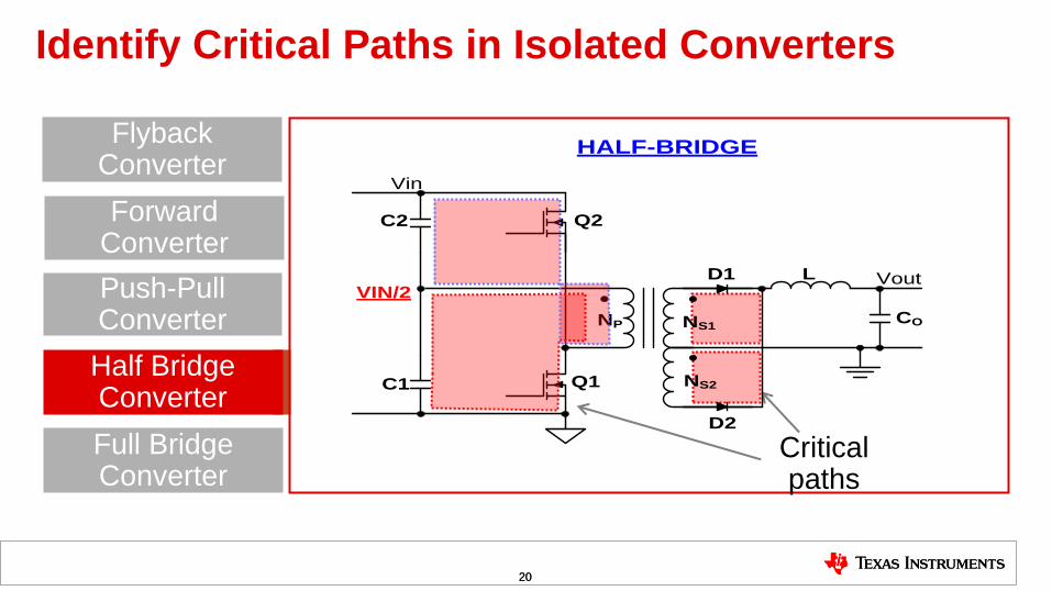
Flyback Converter
Forward Converter
Critical paths
Push-Pull Converter
Half Bridge Converter
Full Bridge Converter
L D1
CO NS1 NP
HALF-BRIDGE
Q1C1
Q2C2
NS2
D2
Vin
VoutVIN/2
21 21
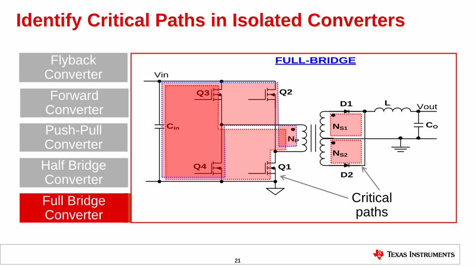
Identify Critical Paths in Isolated Converters
Flyback Converter
Forward Converter
Critical paths
Push-Pull Converter
Half Bridge Converter
Full Bridge Converter
L D1
CO
FULL-BRIDGE
Q1
Q2
D2
Q3
Q4
Vin
Vout
NP
NS1
NS2
Cin
-+
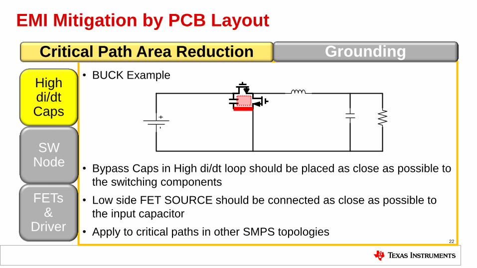
EMI Mitigation by PCB Layout
• BUCK Example
• Bypass Caps in High di/dt loop should be placed as close as possible to
the switching components
• Low side FET SOURCE should be connected as close as possible to
the input capacitor
• Apply to critical paths in other SMPS topologies
22
Critical Path Area Reduction Grounding
High di/dt Caps
SW Node
FETs &
Driver
23
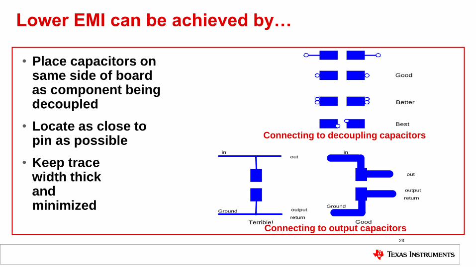
Lower EMI can be achieved by…
• Place capacitors on same side of board as component being decoupled
• Locate as close to pin as possible
• Keep trace width thick and minimized
Connecting to decoupling capacitors
Good
Better
Best
Terrible!
output
Good
inout
Ground output
return
in
out
Ground
return
Connecting to output capacitors
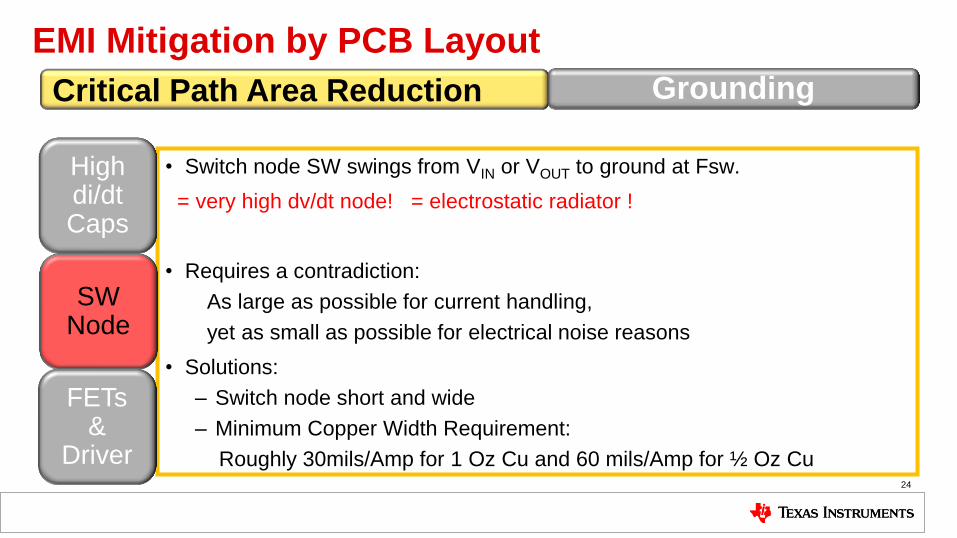
EMI Mitigation by PCB Layout
• Switch node SW swings from VIN or VOUT to ground at Fsw.
= very high dv/dt node! = electrostatic radiator !
• Requires a contradiction:
As large as possible for current handling,
yet as small as possible for electrical noise reasons
• Solutions:
– Switch node short and wide
– Minimum Copper Width Requirement:
Roughly 30mils/Amp for 1 Oz Cu and 60 mils/Amp for ½ Oz Cu
24
Critical Path Area Reduction Grounding
High di/dt Caps
SW Node
FETs &
Driver
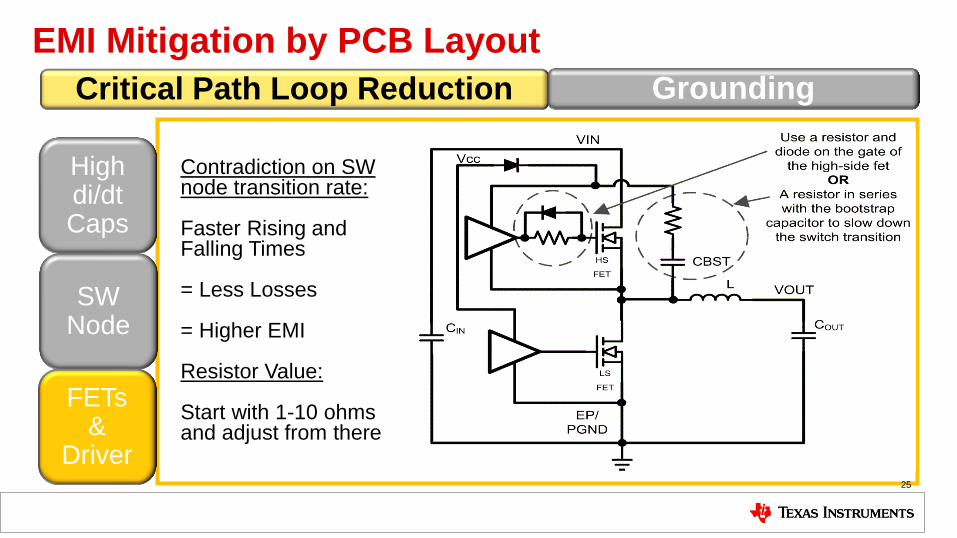
EMI Mitigation by PCB Layout
25
Critical Path Loop Reduction Grounding
High di/dt Caps
SW Node
FETs &
Driver
Contradiction on SW node transition rate: Faster Rising and Falling Times = Less Losses = Higher EMI Resistor Value: Start with 1-10 ohms and adjust from there

EMI Mitigation by PCB Layout
• Ground Plane
– Return Current takes the least IMPEDANCE path
– Unbroken Ground Plane provides shortest return path – image current return path:
26
Critical Path Loop Reduction Grounding
Current flow in top layer trace
Ground
Plane
Return current path in unbroken ground
plane directly under path:
Area minimized & B field minimized
Trace or Cut on the ground plane
Ground
Plane
Return current path enclose much
larger area if the direct path is blocked !
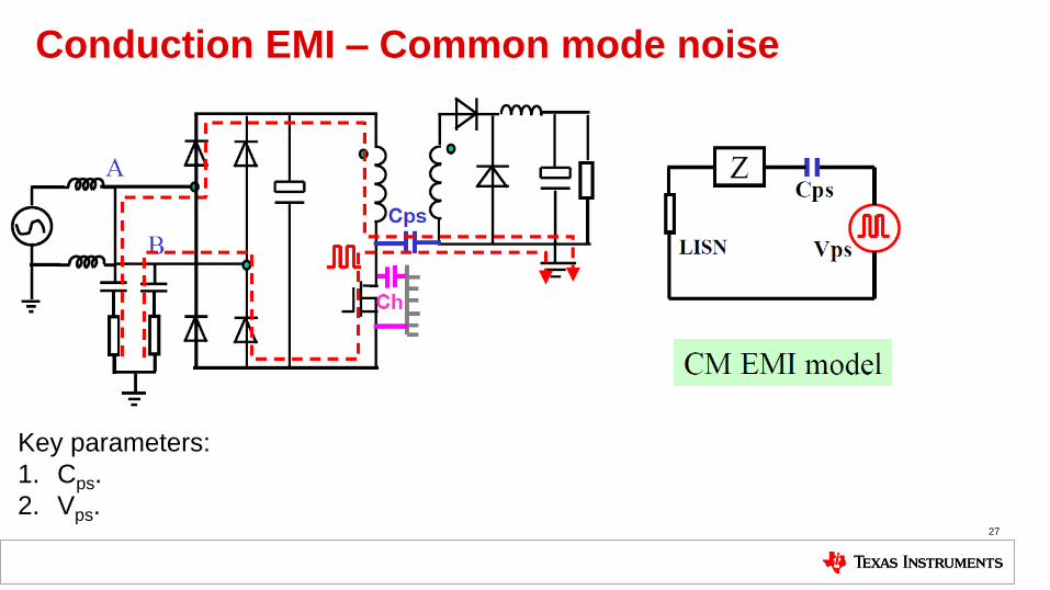
Conduction EMI – Common mode noise
27
Key parameters:
1. Cps.
2. Vps.
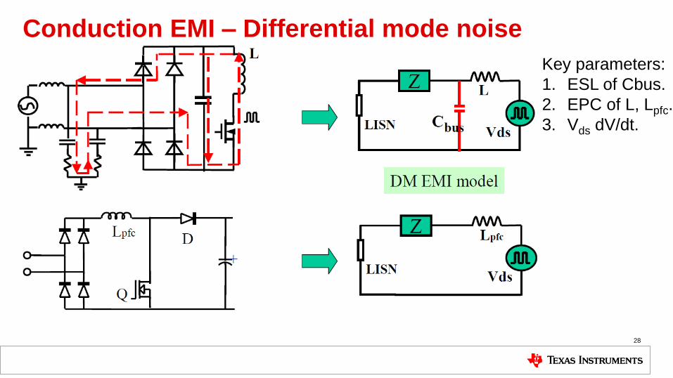
Conduction EMI – Differential mode noise
28
Key parameters:
1. ESL of Cbus.
2. EPC of L, Lpfc.
3. Vds dV/dt.
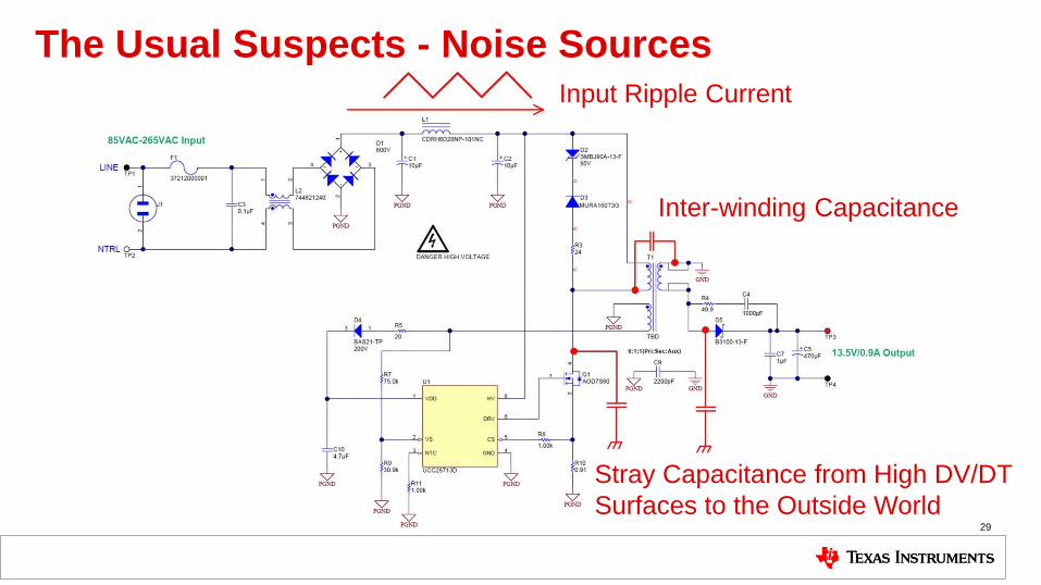
The Usual Suspects - Noise Sources
29
Input Ripple Current
Inter-winding Capacitance
Stray Capacitance from High DV/DT
Surfaces to the Outside World
Conduction EMI – Lower transformer CPS
30
Target: lower CPS to reduce CM noise.
Possible actions:
1. Increase the distance between primary and secondary.
• Side effect: larger leakage and larger losses.
2. Decrease the facing area between primary and secondary.
• Side effect: larger leakage and larger losses.
3. Shielding.
• Side effect: increase cost and need more space.
4. Suitable terminal connection: easy and a must do!
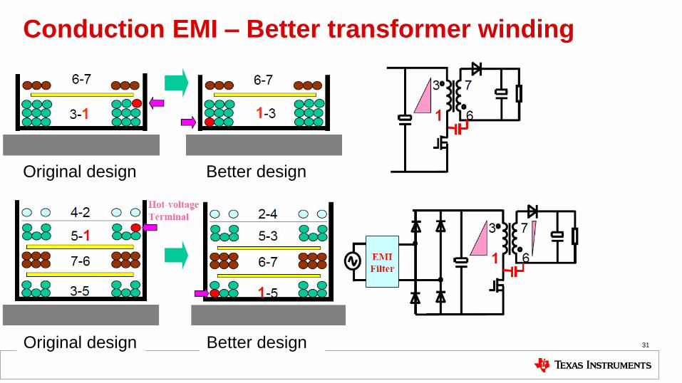
Conduction EMI – Better transformer winding
31
Original design Better design
Original design Better design
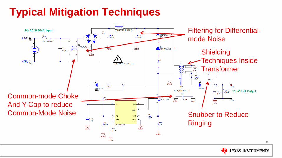
Typical Mitigation Techniques
32
Common-mode Choke
And Y-Cap to reduce
Common-Mode Noise
Filtering for Differential-
mode Noise
Snubber to Reduce
Ringing
Shielding
Techniques Inside
Transformer
Rectifier Location in Flyback Converter
• Rectifier in return lead of transformer
• CIN/CEMI/COUT couple dot end of primary
and non-dot end of secondary to 0 Vac
• Maximum voltage potential between windings
• AC current flows in transformer capacitance,
resulting in common mode current flow and
EMI issues
33
0 Vac
0 Vac
CINCOUT
CEMI
Iac ≠ 0
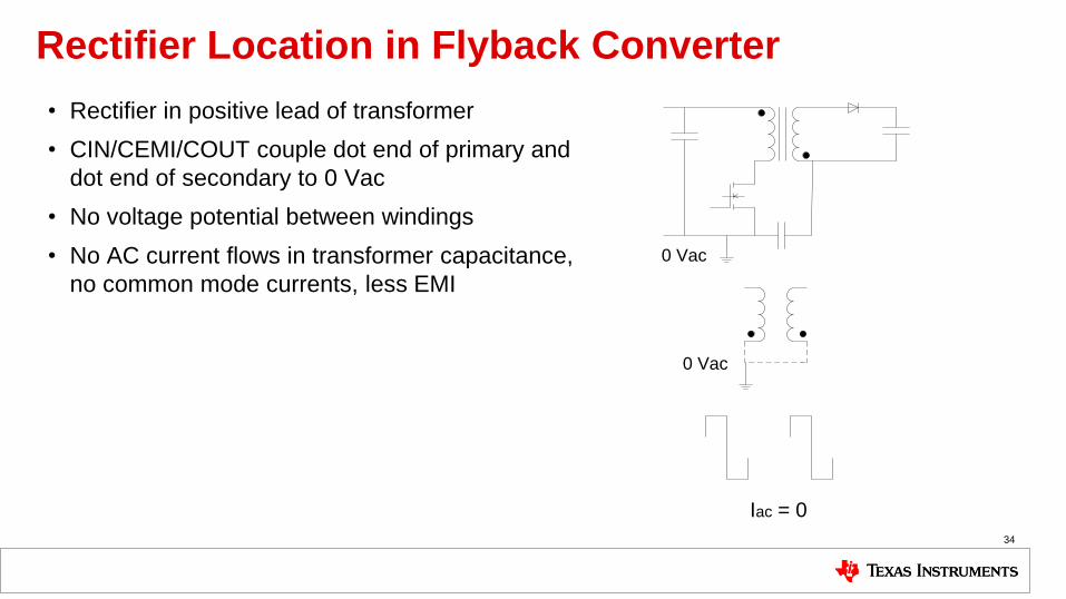
Rectifier Location in Flyback Converter
• Rectifier in positive lead of transformer
• CIN/CEMI/COUT couple dot end of primary and
dot end of secondary to 0 Vac
• No voltage potential between windings
• No AC current flows in transformer capacitance,
no common mode currents, less EMI
34
0 Vac
0 Vac
Iac = 0
35
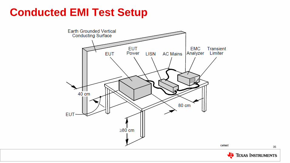
Conducted EMI Test Setup
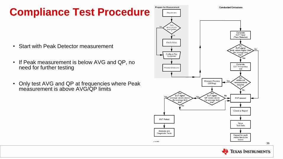
Compliance Test Procedure
36
• Start with Peak Detector measurement
• If Peak measurement is below AVG and QP, no need for further testing
• Only test AVG and QP at frequencies where Peak measurement is above AVG/QP limits
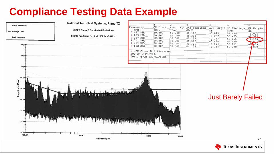
Compliance Testing Data Example
37
Just Barely Failed
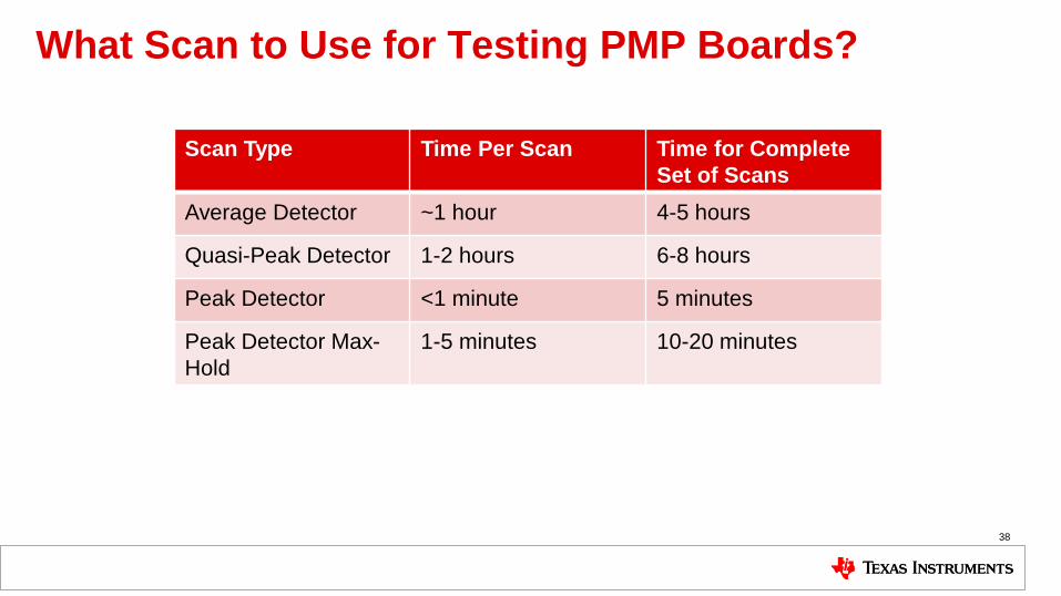
What Scan to Use for Testing PMP Boards?
38
Scan Type Time Per Scan Time for Complete
Set of Scans
Average Detector ~1 hour 4-5 hours
Quasi-Peak Detector 1-2 hours 6-8 hours
Peak Detector <1 minute 5 minutes
Peak Detector Max-
Hold
1-5 minutes 10-20 minutes