Embed Size (px)
Citation preview
Subscriber access provided by Caltech Library Services
The Journal of Physical Chemistry C is published by the American Chemical Society.1155 Sixteenth Street N.W., Washington, DC 20036Published by American Chemical Society. Copyright © American Chemical Society.However, no copyright claim is made to original U.S. Government works, or worksproduced by employees of any Commonwealth realm Crown government in the courseof their duties.
Article
Synthesis and Characterization of PhotoreactiveTiO
2
/Carbon Nanosheet CompositesMert Kurttepeli, Shaoren Deng, Sammy Walter Verbruggen, Giulio Guzzinati, Daire J. Cott,
Silvia Lenaerts, Johan Verbeeck, Gustaaf Van Tendeloo, Christophe Detavernier, and Sara BalsJ. Phys. Chem. C, Just Accepted Manuscript • DOI: 10.1021/jp5067499 • Publication Date (Web): 22 Aug 2014
Downloaded from http://pubs.acs.org on August 24, 2014
Just Accepted
“Just Accepted” manuscripts have been peer-reviewed and accepted for publication. They are postedonline prior to technical editing, formatting for publication and author proofing. The American ChemicalSociety provides “Just Accepted” as a free service to the research community to expedite thedissemination of scientific material as soon as possible after acceptance. “Just Accepted” manuscriptsappear in full in PDF format accompanied by an HTML abstract. “Just Accepted” manuscripts have beenfully peer reviewed, but should not be considered the official version of record. They are accessible to allreaders and citable by the Digital Object Identifier (DOI®). “Just Accepted” is an optional service offeredto authors. Therefore, the “Just Accepted” Web site may not include all articles that will be publishedin the journal. After a manuscript is technically edited and formatted, it will be removed from the “JustAccepted” Web site and published as an ASAP article. Note that technical editing may introduce minorchanges to the manuscript text and/or graphics which could affect content, and all legal disclaimersand ethical guidelines that apply to the journal pertain. ACS cannot be held responsible for errorsor consequences arising from the use of information contained in these “Just Accepted” manuscripts.
1
Synthesis and Characterization of Photoreactive
TiO2/Carbon Nanosheet Composites
Mert Kurttepeli ‡, a
, Shaoren Deng ‡, b
, Sammy W. Verbruggen c, d
, Giulio Guzzinati a, Daire J.
Cott e, Silvia Lenaerts
c, Jo Verbeeck
a, Gustaaf Van Tendeloo
a, Christophe Detavernier
b and
Sara Bals*, a
a EMAT, University of Antwerp, Groenenborgerlaan 171, B-2020 Antwerp, Belgium.
b Department of Solid State Science, University Ghent, Krijgslaan 281/S1, B-9000 Ghent,
Belgium.
c Department of Bio-science Engineering, Sustainable Energy and Air Purification, University of
Antwerp, Groenenborgerlaan 171, B-2020 Antwerp, Belgium.
d Department of Microbial and Molecular Systems, Center for Surface Chemistry and Catalysis,
KU Leuven, Kasteelpark 11 Arenberg 23, B-3001 Heverlee, Belgium.
e Imec, 75, Kapeldreef, B-3001 Leuven, Belgium
Page 1 of 24
ACS Paragon Plus Environment
The Journal of Physical Chemistry
123456789101112131415161718192021222324252627282930313233343536373839404142434445464748495051525354555657585960
2
ABSTRACT
We report the atomic layer deposition of titanium dioxide on carbon nanosheet templates and
investigate the effects of post-deposition annealing in a helium environment using different
characterization techniques. The crystallization of the titanium dioxide coating upon annealing is
observed using in-situ X-ray diffraction. The (micro)-structural characterization of the films is
carried out by scanning electron microscopy and advanced transmission electron microscopy
techniques. Our study shows that the annealing of the atomic layer deposition processed and
carbon nanosheets templated titanium dioxide layers in helium environment results in the
formation of a porous, nanocrystalline and photocatalytically active titanium dioxide-carbon
nanosheet composite film. Such composites are suitable for photocatalysis and dye-sensitized
solar cells applications.
KEYWORDS titanium dioxide, atomic layer deposition, transmission electron microscopy,
photocatalysis, electron tomography.
Page 2 of 24
ACS Paragon Plus Environment
The Journal of Physical Chemistry
123456789101112131415161718192021222324252627282930313233343536373839404142434445464748495051525354555657585960
3
1. INTRODUCTION
Since the discovery of the photocatalytic splitting of water on a titanium dioxide (TiO2)
electrode under ultraviolet (UV) light, TiO2 materials have been subject to extensive research for
many promising applications, such as photovoltaics and photocatalysis.1–3 For such applications,
the surface area and crystallinity are two important material properties which affect the
photovoltaic and photocatalytic efficiency of mesoporous TiO2 materials.4 In order to synthesize
TiO2 with a large surface area, a variety of methods has been employed, including sol-gel,
magnetron-sputtering and chemical vapor deposition.5–7 Atomic layer deposition (ALD) is an
alternative method to produce TiO2 with a large surface area using a template structure.8
Amongst others, carbon nanosheets (CNSs) are widely used as templates for metal/metal oxide
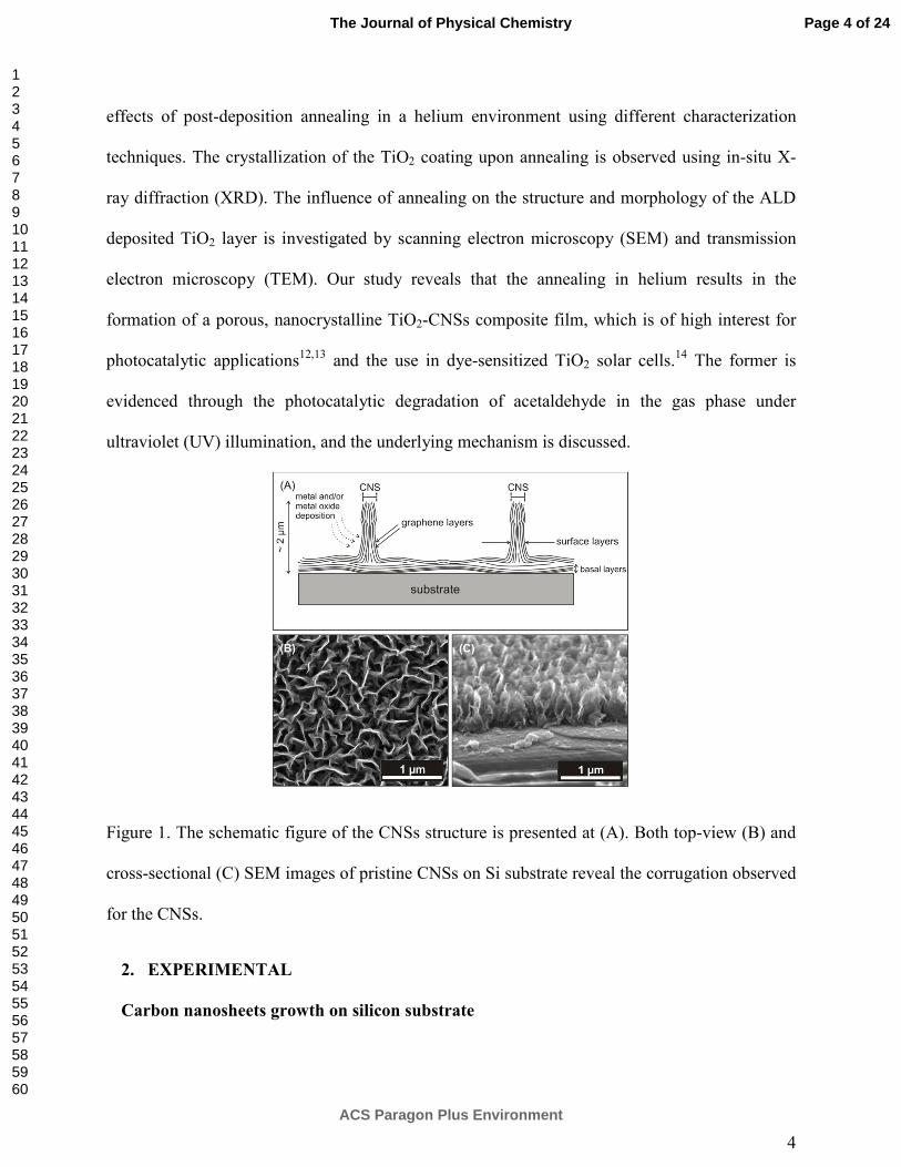
depositions due to their distinct properties, such as high surface area. As illustrated in Fig. 1-(A),
the CNSs consist of several graphene layers that are slightly curved at the nano-scale, which in
return builds up the CNSs morphology that is highly corrugated at the micro-scale (see Fig. 1-(B)
and (C)). Through the ALD method, the presence of the CNSs between the substrate and TiO2
coating also permits having a conducting pathway, which is attractive for photovoltaics and
battery applications.8,9 It was previously found that the post-deposition annealing of ALD-
processed TiO2 materials can lead to a phase transformation from amorphous to anatase-TiO2,
which is the phase that yields the most ideal photocatalytic properties.10 On the other hand, the
annealing environment is known to have a significant effect on the preservation of carbonaceous
species in composite materials. Post-deposition calcination in ambient air, which is a typical
choice as an annealing environment for mesoporous TiO2 materials, usually results in the
removal of carbonaceous species, such as carbon nanotubes (CNTs), through air oxidation.11 In
this paper, we report the atomic layer deposition of TiO2 on CNSs templates and investigate the
Page 3 of 24
ACS Paragon Plus Environment
The Journal of Physical Chemistry
123456789101112131415161718192021222324252627282930313233343536373839404142434445464748495051525354555657585960
4
effects of post-deposition annealing in a helium environment using different characterization
techniques. The crystallization of the TiO2 coating upon annealing is observed using in-situ X-
ray diffraction (XRD). The influence of annealing on the structure and morphology of the ALD
deposited TiO2 layer is investigated by scanning electron microscopy (SEM) and transmission
electron microscopy (TEM). Our study reveals that the annealing in helium results in the
formation of a porous, nanocrystalline TiO2-CNSs composite film, which is of high interest for
photocatalytic applications12,13 and the use in dye-sensitized TiO2 solar cells.14 The former is
evidenced through the photocatalytic degradation of acetaldehyde in the gas phase under
ultraviolet (UV) illumination, and the underlying mechanism is discussed.
Figure 1. The schematic figure of the CNSs structure is presented at (A). Both top-view (B) and
cross-sectional (C) SEM images of pristine CNSs on Si substrate reveal the corrugation observed
for the CNSs.
2. EXPERIMENTAL
Carbon nanosheets growth on silicon substrate
Page 4 of 24
ACS Paragon Plus Environment
The Journal of Physical Chemistry
123456789101112131415161718192021222324252627282930313233343536373839404142434445464748495051525354555657585960
5
CNSs were grown on silicon (Si) wafers with a 200 mm diameter using a recently outlined
procedure.15 Briefly, Si wafers (p-type) were cleaned in a SC1 (APM) mixture to remove
particles and placed in a capacitive coupled plasma enhanced (13.56 MHz) chemical vapor
deposition chamber (Oxford Instruments Plasma Technology). To prepare the wafer surface, a
H2 plasma pre-treatment (300 W) was carried out for 5 minutes at 0.45 Torr and 750 °C. Next,
C2H2/H2 was flowed in a flow ratio of 1:10 into the chamber and a 300 W plasma at a total
pressure of 0.45 Torr was maintained for 45 minutes. The substrate was removed from the
chamber and allowed to cool under vacuum (10-4 Torr) for 5 minutes.
ALD-based synthesis and annealing of TiO2 nanostructures
As-grown CNSs on a Si substrate were loaded into a homemade ALD tool with a base pressure
in the low 10-7 mbar range. The sample was placed onto a chuck, and heated to 100°C. Tetrakis
(dimethylamido) titanium (TDMAT) (99.999% Sigma-Aldrich) and O3 gas generated by an
ozone generator (Yanco Industries LTD) were alternately pulsed into the ALD chamber at
pressures of 0.3 and 0.5 mbar, respectively. In our previous study, we found that 200 ALD cycles
of TiO2 on CNSs which is annealed contrarily in ambient air results in a catalyst film that
outperforms a PC500 reference sample, in other words showing the optimum photocatalytic
activity.16 Therefore, 200 ALD-cycles have been likewise applied on the CNSs template. In the
flux the concentration of the ozone was 145 µg/mL. 20 seconds pulse time and 40 seconds pump
time were used for a conformal coating of TiO2 on the entire CNSs and to prevent the occurrence
of chemical vapor deposition type reactions.
The occurrence of the phase transformations in the TiO2 films upon annealing were monitored
using in-situ X-ray diffraction (in-situ XRD) with a dedicated Bruker D8 system.17 The sample
was annealed from 20°C to 600°C at a rate of 1°C per minute in helium monitored by a K-type
Page 5 of 24
ACS Paragon Plus Environment
The Journal of Physical Chemistry
123456789101112131415161718192021222324252627282930313233343536373839404142434445464748495051525354555657585960
6
thermocouple and kept at 600°C for 3 hours while being illuminated by Cu Kα radiation
(wavelength 0.154 nm). Diffracted X-rays were captured by a linear detector covering a range of
20° in 2θ set to a collection time of 5 seconds.
SEM and TEM characterizations
SEM was performed using a FEI Helios NanoLab 650 dual-beam system to resolve the
morphology of the films during the synthesis and after annealing. TEM specimens were prepared
from the sample and studied with a variety of techniques in order to obtain more detailed
information. Several samples were prepared by scraping off the TiO2-CNSs composite film from
the silicon substrate surface and suspending the resulting product in ethanol. A drop of this
suspension was deposited on a carbon coated TEM grid. Also cross-section samples were
prepared by polishing thin-cut slices of the material using mechanical grinding, and consequent
thinning in a precision ion polishing system (Gatan Duo Mill 600). Bright-field TEM (BFTEM)
and high-resolution TEM (HRTEM) were performed using a FEI Tecnai F20 operated at 200 kV.
High-angle annular dark field scanning TEM (HAADF-STEM) images and energy-dispersive X-
ray elemental maps were collected using an aberration corrected cubed FEI Titan operated at 300
kV, equipped with a Super-X detector for EDX analysis. The HAADF-STEM images were
recorded using probes with convergence semi-angles in the 21−25 mrad range with a probe size
of about 1 Å. Energy filtered TEM (EFTEM) elemental maps were collected using a Philips
CM30-FEG microscope operated at 300 kV.
Tilt series for electron tomography were acquired on cross-section TEM specimen with the
aberration corrected cubed FEI Titan operated at 200 kV in combination with an advanced
tomography holder from Fischione Instruments and the FEI XPlore3D acquisition software. Tilt
series consisting of 71 HAADF-STEM images were acquired with tilt increments of 2° over a
Page 6 of 24
ACS Paragon Plus Environment
The Journal of Physical Chemistry
123456789101112131415161718192021222324252627282930313233343536373839404142434445464748495051525354555657585960
7
range of ±70° on cross-section TEM samples. Alignment of the data was carried out using the
FEI Inspect3D software package. The reconstruction was performed using the “Simultaneous
Iterative Reconstruction Technique” (SIRT) with 25 iterations implemented in Inspect3D. Amira
(Visage Imaging GmbH) was used for the visualization of the reconstructed volume.
Scanning TEM-electron energy loss spectroscopy (STEM-EELS) experiments were carried out
on cross-section TEM specimens using a double aberration corrected cubed FEI Titan operated
at 120 kV, equipped with a monochromator to optimize the energy resolution for EELS
measurements. Quantitative elemental maps were collected by subtracting a power law
background from the spectra and fitting the corresponding core-loss excitation edges to reference
spectra. The fitting for the acquired spectra was carried out using the EELSModel software
package.18
Photocatalytic activity tests
The evolution of the acetaldehyde concentration together with CO2 formation as the
degradation product was continuously monitored using on-line FTIR spectroscopy. More details
on the photocatalytic test can be found in our previous study.19
3. RESULTS
The titanium dioxide coated carbon nanosheets were annealed in a helium environment while
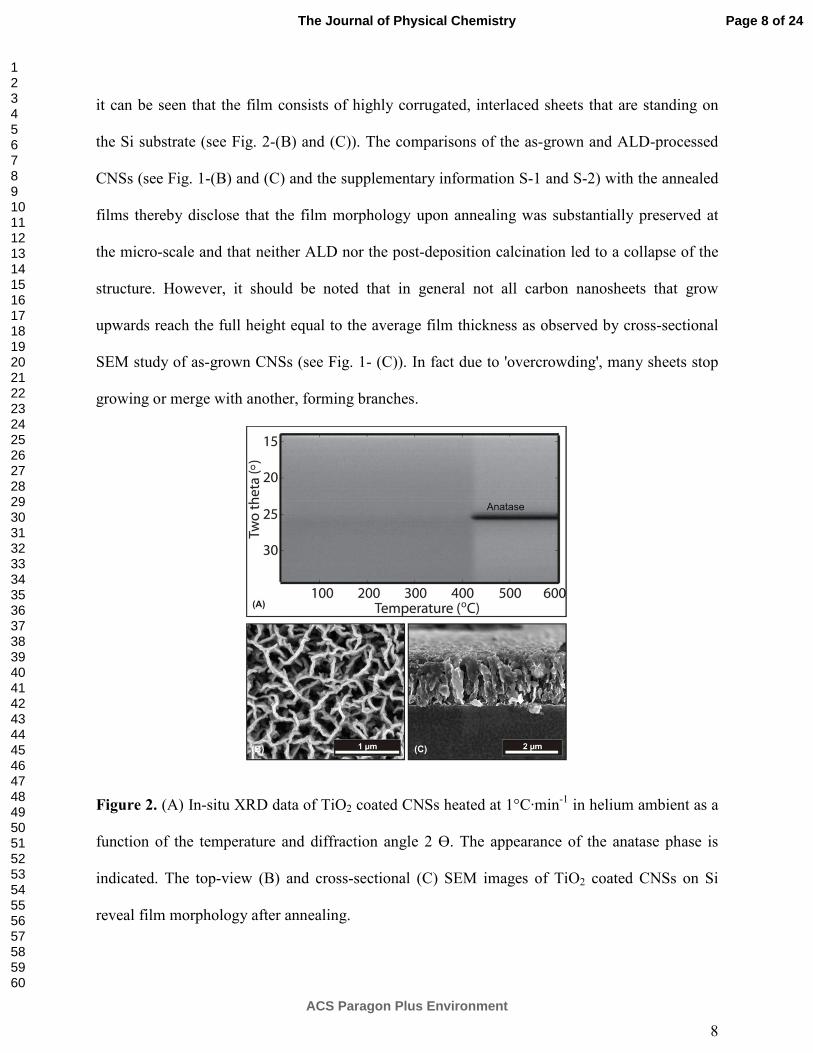
simultaneously monitoring the formation of different phases through in-situ XRD. The results
are presented in Fig. 2-(A). It can be seen that the as-deposited TiO2 film, which was gradually
heated to a temperature of 600°C in He with a ramp rate of 1°C per min, starts to transform into
crystalline anatase at a temperature of 425°C (see Fig. 2-(A)). The broad-band which is centered
at 2θ = 25.1° corresponds to (101) crystallographic planes of the anatase phase. The preliminary
characterization of the resulting film morphology was carried out using SEM. From the images,
Page 7 of 24
ACS Paragon Plus Environment
The Journal of Physical Chemistry
123456789101112131415161718192021222324252627282930313233343536373839404142434445464748495051525354555657585960
8
it can be seen that the film consists of highly corrugated, interlaced sheets that are standing on
the Si substrate (see Fig. 2-(B) and (C)). The comparisons of the as-grown and ALD-processed
CNSs (see Fig. 1-(B) and (C) and the supplementary information S-1 and S-2) with the annealed
films thereby disclose that the film morphology upon annealing was substantially preserved at
the micro-scale and that neither ALD nor the post-deposition calcination led to a collapse of the
structure. However, it should be noted that in general not all carbon nanosheets that grow
upwards reach the full height equal to the average film thickness as observed by cross-sectional
SEM study of as-grown CNSs (see Fig. 1- (C)). In fact due to 'overcrowding', many sheets stop
growing or merge with another, forming branches.
Figure 2. (A) In-situ XRD data of TiO2 coated CNSs heated at 1°C·min-1 in helium ambient as a
function of the temperature and diffraction angle 2 Ɵ. The appearance of the anatase phase is
indicated. The top-view (B) and cross-sectional (C) SEM images of TiO2 coated CNSs on Si
reveal film morphology after annealing.
Page 8 of 24
ACS Paragon Plus Environment
The Journal of Physical Chemistry
123456789101112131415161718192021222324252627282930313233343536373839404142434445464748495051525354555657585960
9
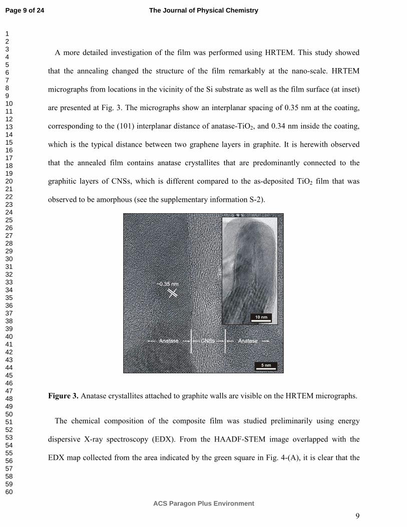
A more detailed investigation of the film was performed using HRTEM. This study showed
that the annealing changed the structure of the film remarkably at the nano-scale. HRTEM
micrographs from locations in the vicinity of the Si substrate as well as the film surface (at inset)
are presented at Fig. 3. The micrographs show an interplanar spacing of 0.35 nm at the coating,
corresponding to the (101) interplanar distance of anatase-TiO2, and 0.34 nm inside the coating,
which is the typical distance between two graphene layers in graphite. It is herewith observed
that the annealed film contains anatase crystallites that are predominantly connected to the
graphitic layers of CNSs, which is different compared to the as-deposited TiO2 film that was
observed to be amorphous (see the supplementary information S-2).
Figure 3. Anatase crystallites attached to graphite walls are visible on the HRTEM micrographs.
The chemical composition of the composite film was studied preliminarily using energy
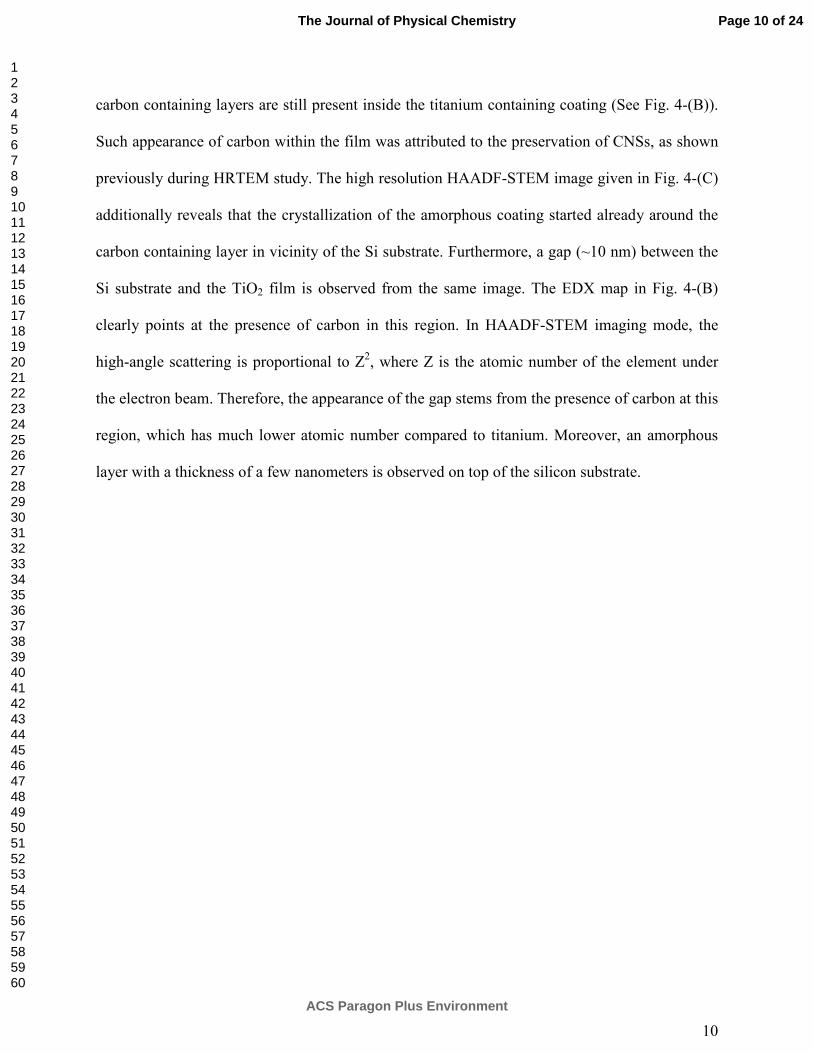
dispersive X-ray spectroscopy (EDX). From the HAADF-STEM image overlapped with the
EDX map collected from the area indicated by the green square in Fig. 4-(A), it is clear that the
Page 9 of 24
ACS Paragon Plus Environment
The Journal of Physical Chemistry
123456789101112131415161718192021222324252627282930313233343536373839404142434445464748495051525354555657585960
10
carbon containing layers are still present inside the titanium containing coating (See Fig. 4-(B)).
Such appearance of carbon within the film was attributed to the preservation of CNSs, as shown
previously during HRTEM study. The high resolution HAADF-STEM image given in Fig. 4-(C)
additionally reveals that the crystallization of the amorphous coating started already around the
carbon containing layer in vicinity of the Si substrate. Furthermore, a gap (~10 nm) between the
Si substrate and the TiO2 film is observed from the same image. The EDX map in Fig. 4-(B)
clearly points at the presence of carbon in this region. In HAADF-STEM imaging mode, the
high-angle scattering is proportional to Z2, where Z is the atomic number of the element under
the electron beam. Therefore, the appearance of the gap stems from the presence of carbon at this
region, which has much lower atomic number compared to titanium. Moreover, an amorphous
layer with a thickness of a few nanometers is observed on top of the silicon substrate.
Page 10 of 24
ACS Paragon Plus Environment
The Journal of Physical Chemistry
123456789101112131415161718192021222324252627282930313233343536373839404142434445464748495051525354555657585960
11
Figure 4. Cross-sectional HAADF-STEM image (A) reveals the film morphology. The carbon,
silicon and titanium composition of the nanosheets can be seen on (B) the EDX mixed colour
elemental map. High resolution HAADF-STEM image (C) from a region highlighted by the red
square at the HAADF-STEM image (A) reveals the growth of CNSs to be along the Si <100>
direction according to the diffractogram shown on the inset.
To investigate the 3-D structure of the material, HAADF-STEM electron tomography was
performed. Visualization of the 3-D reconstructed volume of TiO2/CNSs composite film is
shown in Fig. 5 (A). An animated version of the tomogram is also provided in the supporting
information as a video. The study revealed that the composite film yields a highly porous
Page 11 of 24
ACS Paragon Plus Environment
The Journal of Physical Chemistry
123456789101112131415161718192021222324252627282930313233343536373839404142434445464748495051525354555657585960
12
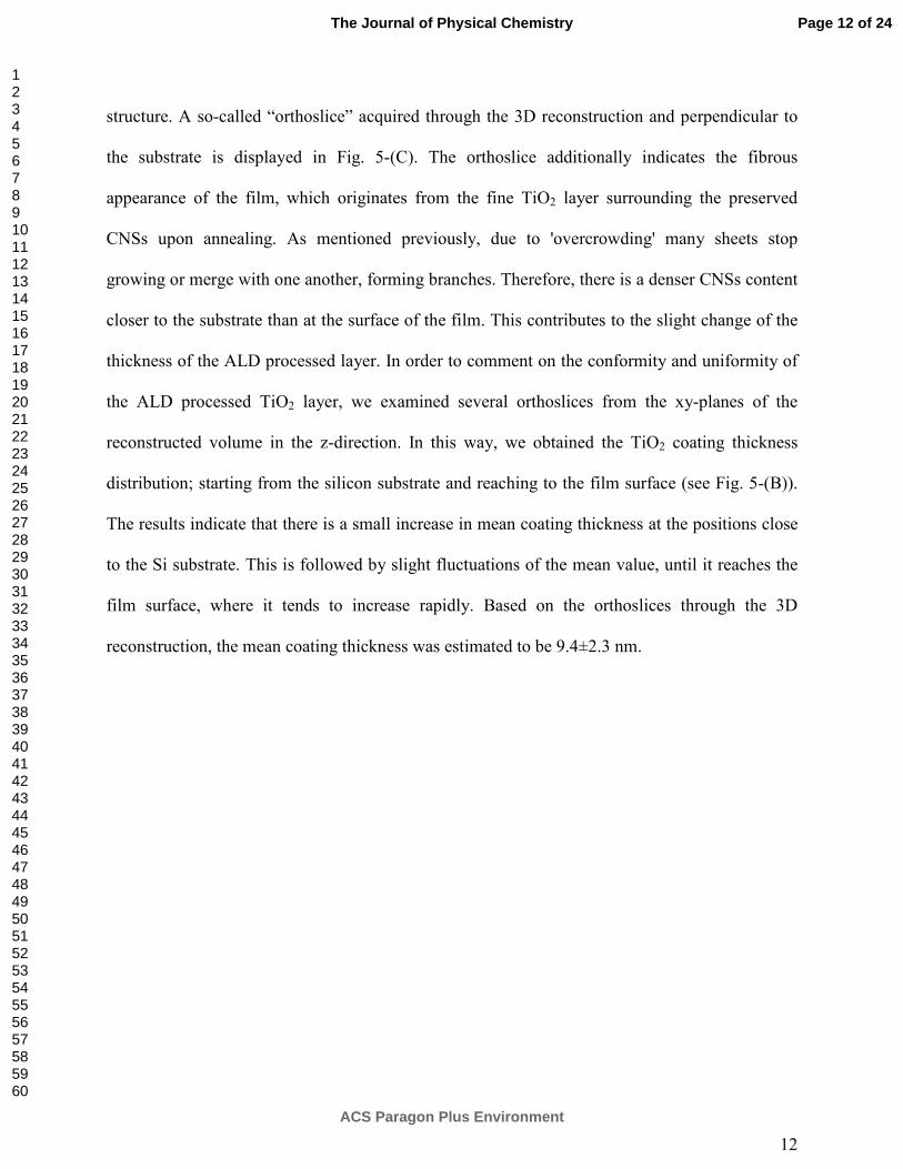
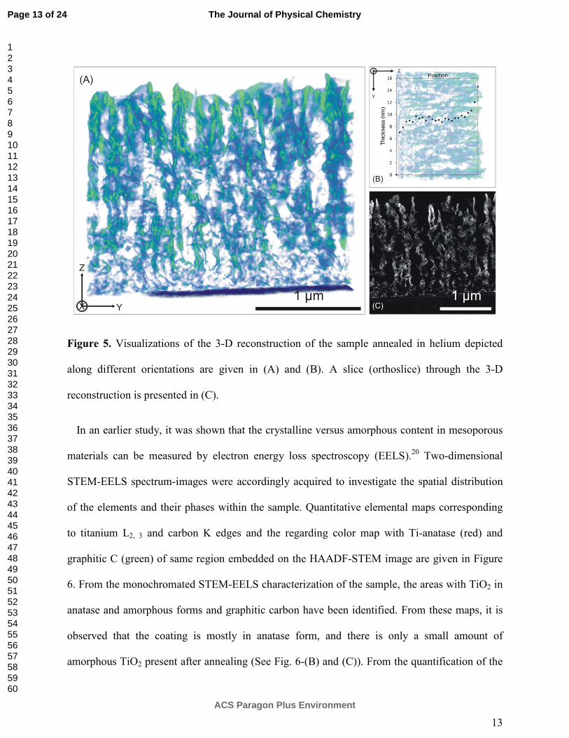
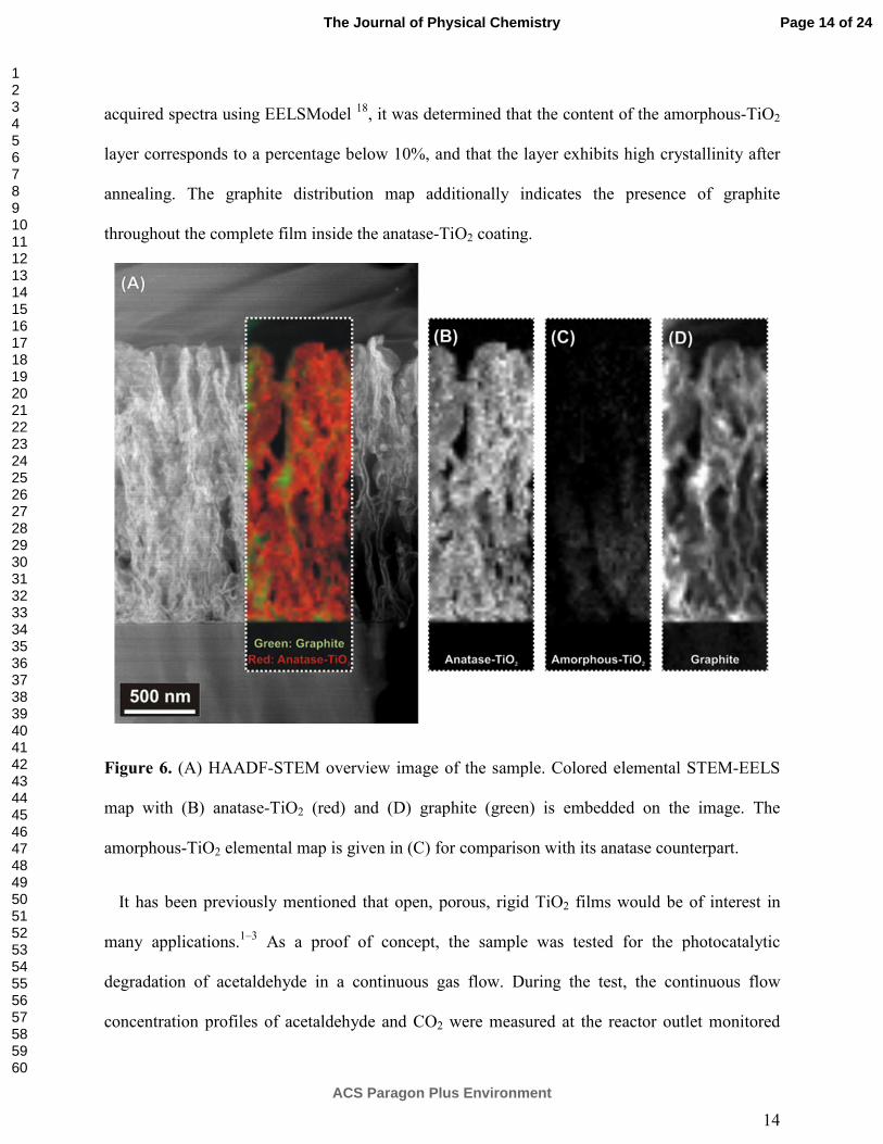
structure. A so-called “orthoslice” acquired through the 3D reconstruction and perpendicular to
the substrate is displayed in Fig. 5-(C). The orthoslice additionally indicates the fibrous
appearance of the film, which originates from the fine TiO2 layer surrounding the preserved
CNSs upon annealing. As mentioned previously, due to 'overcrowding' many sheets stop
growing or merge with one another, forming branches. Therefore, there is a denser CNSs content
closer to the substrate than at the surface of the film. This contributes to the slight change of the
thickness of the ALD processed layer. In order to comment on the conformity and uniformity of
the ALD processed TiO2 layer, we examined several orthoslices from the xy-planes of the
reconstructed volume in the z-direction. In this way, we obtained the TiO2 coating thickness
distribution; starting from the silicon substrate and reaching to the film surface (see Fig. 5-(B)).
The results indicate that there is a small increase in mean coating thickness at the positions close
to the Si substrate. This is followed by slight fluctuations of the mean value, until it reaches the
film surface, where it tends to increase rapidly. Based on the orthoslices through the 3D
reconstruction, the mean coating thickness was estimated to be 9.4±2.3 nm.
Page 12 of 24
ACS Paragon Plus Environment
The Journal of Physical Chemistry
123456789101112131415161718192021222324252627282930313233343536373839404142434445464748495051525354555657585960
13
Figure 5. Visualizations of the 3-D reconstruction of the sample annealed in helium depicted
along different orientations are given in (A) and (B). A slice (orthoslice) through the 3-D
reconstruction is presented in (C).
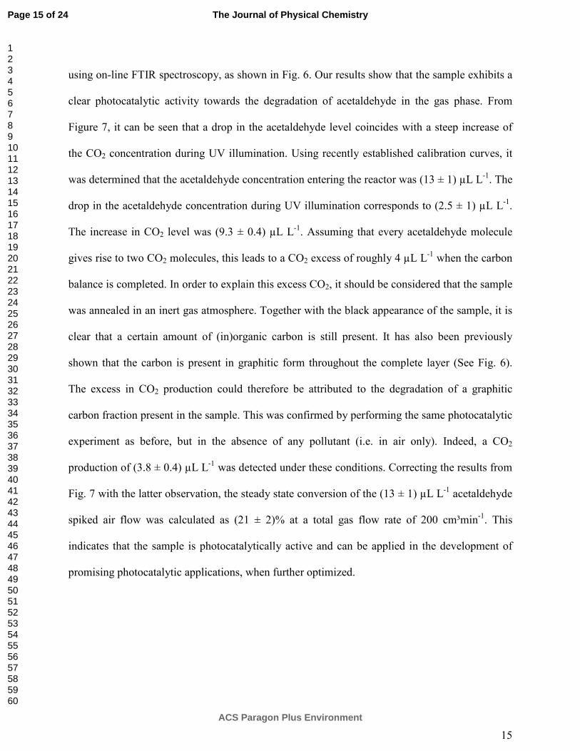
In an earlier study, it was shown that the crystalline versus amorphous content in mesoporous
materials can be measured by electron energy loss spectroscopy (EELS).20 Two-dimensional
STEM-EELS spectrum-images were accordingly acquired to investigate the spatial distribution
of the elements and their phases within the sample. Quantitative elemental maps corresponding
to titanium L2, 3 and carbon K edges and the regarding color map with Ti-anatase (red) and
graphitic C (green) of same region embedded on the HAADF-STEM image are given in Figure
6. From the monochromated STEM-EELS characterization of the sample, the areas with TiO2 in
anatase and amorphous forms and graphitic carbon have been identified. From these maps, it is
observed that the coating is mostly in anatase form, and there is only a small amount of
amorphous TiO2 present after annealing (See Fig. 6-(B) and (C)). From the quantification of the
Page 13 of 24
ACS Paragon Plus Environment
The Journal of Physical Chemistry
123456789101112131415161718192021222324252627282930313233343536373839404142434445464748495051525354555657585960
14
acquired spectra using EELSModel 18, it was determined that the content of the amorphous-TiO2
layer corresponds to a percentage below 10%, and that the layer exhibits high crystallinity after
annealing. The graphite distribution map additionally indicates the presence of graphite
throughout the complete film inside the anatase-TiO2 coating.
Figure 6. (A) HAADF-STEM overview image of the sample. Colored elemental STEM-EELS
map with (B) anatase-TiO2 (red) and (D) graphite (green) is embedded on the image. The
amorphous-TiO2 elemental map is given in (C) for comparison with its anatase counterpart.
It has been previously mentioned that open, porous, rigid TiO2 films would be of interest in
many applications.1–3 As a proof of concept, the sample was tested for the photocatalytic
degradation of acetaldehyde in a continuous gas flow. During the test, the continuous flow
concentration profiles of acetaldehyde and CO2 were measured at the reactor outlet monitored
Page 14 of 24
ACS Paragon Plus Environment
The Journal of Physical Chemistry
123456789101112131415161718192021222324252627282930313233343536373839404142434445464748495051525354555657585960
15
using on-line FTIR spectroscopy, as shown in Fig. 6. Our results show that the sample exhibits a
clear photocatalytic activity towards the degradation of acetaldehyde in the gas phase. From
Figure 7, it can be seen that a drop in the acetaldehyde level coincides with a steep increase of
the CO2 concentration during UV illumination. Using recently established calibration curves, it
was determined that the acetaldehyde concentration entering the reactor was (13 ± 1) µL L-1. The
drop in the acetaldehyde concentration during UV illumination corresponds to (2.5 ± 1) µL L-1.
The increase in CO2 level was (9.3 ± 0.4) µL L-1. Assuming that every acetaldehyde molecule
gives rise to two CO2 molecules, this leads to a CO2 excess of roughly 4 µL L-1 when the carbon
balance is completed. In order to explain this excess CO2, it should be considered that the sample
was annealed in an inert gas atmosphere. Together with the black appearance of the sample, it is
clear that a certain amount of (in)organic carbon is still present. It has also been previously
shown that the carbon is present in graphitic form throughout the complete layer (See Fig. 6).
The excess in CO2 production could therefore be attributed to the degradation of a graphitic
carbon fraction present in the sample. This was confirmed by performing the same photocatalytic
experiment as before, but in the absence of any pollutant (i.e. in air only). Indeed, a CO2
production of (3.8 ± 0.4) µL L-1 was detected under these conditions. Correcting the results from
Fig. 7 with the latter observation, the steady state conversion of the (13 ± 1) µL L-1 acetaldehyde
spiked air flow was calculated as (21 ± 2)% at a total gas flow rate of 200 cm³min-1. This
indicates that the sample is photocatalytically active and can be applied in the development of
promising photocatalytic applications, when further optimized.
Page 15 of 24
ACS Paragon Plus Environment
The Journal of Physical Chemistry
123456789101112131415161718192021222324252627282930313233343536373839404142434445464748495051525354555657585960

16
Figure 7. Continuous flow concentration profiles of acetaldehyde and CO2 measured at the
reactor outlet monitored using on-line FTIR spectroscopy. Dark and UV conditions are indicated
in the graph.
Discussion
Our results demonstrate that ALD is a powerful technique to synthesize TiO2 nanostructured
films on carbon nanosheet templates. The characterization performed in this work shows that the
ALD-process results in the formation of an amorphous TiO2 coating surrounding the CNSs (see
the supporting information S-2). In a related study21 in which TiO2 films were grown from TiCl4
and H2O in a flow type low-pressure ALD reactor, it was demonstrated that crystalline anatase
phase only appears at growth temperatures above 150°C. ALD of the TiO2 on CNSs using
TDMAT as precursor employed in our study correspondingly forms a fine, amorphous coating of
TiO2 at a growth temperature of 100 °C, which explains the lack of crystallinity of the as-
deposited film.
The crystallinity of the TiO2 film plays an important role at enhancing the photocatalytic
activity22 and charge transport and photocurrent in dye-sensitized TiO2 solar cells.23 The in-situ
Page 16 of 24
ACS Paragon Plus Environment
The Journal of Physical Chemistry
123456789101112131415161718192021222324252627282930313233343536373839404142434445464748495051525354555657585960
17
XRD measurements indicate that the post-deposition annealing process modifies the film by a
phase transformation from amorphous to crystalline anatase TiO2 (see Fig. 2-(A)). STEM-EELS
characterization of the sample (See Fig. 6) additionally reveals that the TiO2 film exhibits high
crystallinity after annealing. In terms of the phase transformation, the annealing of ALD
processed TiO2 shows resemblance to the annealing of TiO2 nanostructured films deposited via
sol-gel24 or magnetron sputtering25 methods.
The annealed film, as shown by the electron tomography results in Fig 5, presents a uniform,
conformal TiO2 coating. Electron tomography results indicate that the mean thickness of the
coating only slightly varies throughout the film (See Fig. 5-(B)). The small variation of the
coating thickness can be ascribed to the inability of the precursor vapor to flow through the pores
of the template surface which is blocked by the coating material during ALD.26 It is also worth
mentioning that some graphene layers gradually merge into one sheet at the bottom of the film,
thus creating pores or slots with very small openings. In this case, some interior spaces would not
accept more ALD cycles since their bottle necks would be sealed by TiO2 coating after e.g. 50
cycles.27 On the other hand, the porosity is known to be an important property for an efficient
photovoltaic operation, which eases the penetration of light deep into the film. Based on the
electron tomography results, it is revealed that the annealing of the ALD-processed film results
in the formation of a highly porous structure.
With a deeper investigation performed through HRTEM (see Fig. 3) and STEM-EELS (see
Fig. 6), it is discovered that the annealed film still yields graphene layers of CNSs in addition to
the anatase crystallites formed at the walls of CNSs. For dye-sensitized TiO2 solar cell
applications, the preservation of the CNSs upon annealing in helium environment is particularly
important, since this plays a significant role as a conducting template to facilitate charge
Page 17 of 24
ACS Paragon Plus Environment
The Journal of Physical Chemistry
123456789101112131415161718192021222324252627282930313233343536373839404142434445464748495051525354555657585960
18
transport in the composite films for improving the efficiency of nanostructure-based solar energy
conversion devices consisting of CNTs/TiO2 systems.28,29 It is shown here that this can be
obtained by annealing the film in helium environment. As a consequence, the potential of these
nanocomposites in photovoltaic applications is obvious.
Such thin and porous TiO2 films are of particular interest for several applications such as
photocatalysis, as shown in Fig. 7 for the photocatalytic degradation of acetaldehyde in a
continuous polluted air stream. The morphology of the discussed sample is particularly well
suited for gas phase applications, as it presents a very accessible, open and porous TiO2 structure
in mostly anatase form, offering a lot of available active sites.30 Furthermore, as a counterpart to
CNSs, multi-walled carbon nanotubes (MWCNTs) have been widely used as template or support
for catalysis due to their higher surface area than CNSs and other carbonaceous materials.31
However, in our previous study, we found that TiO2 coated MWCNTs annealed in helium
showed no activity in gas phase photocatalytic tests.19 The TEM characterization showed that the
TiO2 nanoparticles coated on MWCNTs were partially crystallized. In the present research, TiO2
coating on planar graphene layers of the CNSs are crystallized adequately when it is annealed in
helium. The TiO2 coating on CNSs crystallize at a temperature around 425°C while in our
previous report, during annealing in helium, TiO2 coatings on MWCNTs started to crystallize at
500°C. This comparison illustrates that the crystallization behavior of TiO2 on graphene layers
also depends on their surface tension. In CNSs, the graphene layers are planar or slightly curved
at short distances, mostly within a few nanometers scale, while in MWCNTs, the graphene layers
are curved to form tubes. This feature of CNSs contributes to the relatively easy crystallization of
TiO2 for photocatalytic applications in comparison to MWCNTs, which has been rarely
discussed before.
Page 18 of 24
ACS Paragon Plus Environment
The Journal of Physical Chemistry
123456789101112131415161718192021222324252627282930313233343536373839404142434445464748495051525354555657585960
19
Conclusions
This study demonstrates the influence of annealing on ALD processed TiO2 nanostructured
films in an inert gas (helium) environment. The morphology of the film was visualized using
conventional TEM imaging techniques, whereas the complex 3D structure of TiO2
nanostructured films was revealed by HAADF–STEM electron tomography. The annealing was
found to cause the ALD processed film to undergo a phase transformation from amorphous to
anatase TiO2. The calcination resulted in highly crystalline TiO2 nanostructures with a porous
network and a large surface area, which are desirable properties for photocatalytic and
photovoltaics applications. TEM characterization indicated that the removal of carbon
nanosheets template is hindered, and thin, porous, nanocrystalline and photocatalytically active
TiO2-carbon nanosheets composite material is produced.
AUTHOR INFORMATION
Corresponding Author
* The corresponding author: Sara Bals, Address: EMAT, University of Antwerp,
Groenenborgerlaan 171, B-2020 Antwerp, Belgium, Telephone Number: +32 (0)32653284, E-
mail Address: [email protected].
Author Contributions
‡These authors contributed equally.
ACKNOWLEDGMENT
This research was funded by the Flemish research foundation FWO-Vlaanderen, by the
European Research Council (Starting Grant No. 239865) and by the Special Research Fund BOF
Page 19 of 24
ACS Paragon Plus Environment
The Journal of Physical Chemistry
123456789101112131415161718192021222324252627282930313233343536373839404142434445464748495051525354555657585960
20
of Ghent University (GOA - 01G01513). Giulio Guzzinati, Mert Kurttepeli, Jo Verbeeck, Sara
Bals and Gustaaf Van Tendeloo acknowledge funding from the European Research Council
under the 7th Framework Program (FP7), ERC Starting Grant No. 278510 VORTEX and No.
335078 COLOURATOMS.
Supporting Information Available. Figure S-1 shows BFTEM and HRTEM micrographs as
well as the EFTEM elemental map from pristine CNSs, and Figure S-2 shows the top-view (A)
and cross-sectional (B) SEM images, BFTEM, HRTEM micrographs and EFTEM elemental
maps of TiO2 coated CNSs prior to annealing. Movie M1 shows the electron tomography movie
from the TiO2 coated CNSs upon annealing. This material is available free of charge via the
Internet at http://pubs.acs.org/.
REFERENCES
(1) Fujishima, A.; Honda, K. Electrochemical Photolysis of Water at a Semiconductor Electrode. Nature 1972, 238, 37–38.
(2) Chen, X.; Mao, S. S. Titanium Dioxide Nanomaterials: Synthesis, Properties, Modifications, and Applications. Chem. Rev. 2007, 107, 2891–2959.
(3) Kay, A.; Grätzel, M. Low Cost Photovoltaic Modules Based on Dye Sensitized Nanocrystalline Titanium Dioxide and Carbon Powder. Sol. Energy Mater. Sol. Cells 1996, 44, 99–117.
(4) Vivero-Escoto, J. L.; Chiang, Y.-D.; Wu, K. C.-W.; Yamauchi, Y. Recent Progress in Mesoporous Titania Materials: Adjusting Morphology for Innovative Applications. Sci. Technol. Adv. Mater. 2012, 13, 013003.
(5) Su, C.; Hong, B.-Y.; Tseng, C.-M. Sol–gel Preparation and Photocatalysis of Titanium Dioxide. Catal. Today 2004, 96, 119–126.
(6) Weinberger, B.; Garber, R. Titanium Dioxide Photocatalysts Produced by Reactive Magnetron Sputtering. Appl. Phys. Lett. 1995, 66, 2409–2411.
Page 20 of 24
ACS Paragon Plus Environment
The Journal of Physical Chemistry
123456789101112131415161718192021222324252627282930313233343536373839404142434445464748495051525354555657585960
21
(7) Li Puma, G.; Bono, A.; Krishnaiah, D.; Collin, J. G. Preparation of Titanium Dioxide Photocatalyst Loaded onto Activated Carbon Support Using Chemical Vapor Deposition: A Review Paper. J. Hazard. Mater. 2008, 157, 209–219.
(8) Rooth, M.; Quinlan, R. A.; Widenkvist, E.; Lu, J.; Grennberg, H.; Holloway, B. C.; Hårsta, A.; Jansson, U. Atomic Layer Deposition of Titanium Dioxide Nanostructures Using Carbon Nanosheets as a Template. J. Cryst. Growth 2009, 311, 373–377.
(9) Ban, C.; Xie, M.; Sun, X.; Travis, J. J.; Wang, G.; Sun, H.; Dillon, A. C.; Lian, J.; George, S. M. Atomic Layer Deposition of Amorphous TiO2 on Graphene as an Anode for Li-Ion Batteries. Nanotechnology 2013, 24, 424002.
(10) Ovenstone, J.; Yanagisawa, K. Effect of Hydrothermal Treatment of Amorphous Titania on the Phase Change from Anatase to Rutile during Calcination. Chem. Mater. 1999, 32, 2770–2774.
(11) Yang, Y.; Qu, L.; Dai, L.; Kang, T.-S.; Durstock, M. Electrophoresis Coating of Titanium Dioxide on Aligned Carbon Nanotubes for Controlled Syntheses of Photoelectronic Nanomaterials. Adv. Mater. 2007, 19, 1239–1243.
(12) Pore, V.; Rahtu, A.; Leskelä, M.; Ritala, M.; Sajavaara, T.; Keinonen, J. Atomic Layer Deposition of Photocatalytic TiO2 Thin Films from Titanium Tetramethoxide and Water. Chem. Vap. Depos. 2004, 10, 143–148.
(13) Fateh, R.; Ismail, A. A.; Dillert, R.; Bahnemann, D. W. Highly Active Crystalline Mesoporous TiO2 Films Coated onto Polycarbonate Substrates for Self-Cleaning Applications. J. Phys. Chem. C 2011, 115, 10405–10411.
(14) Williams, V. O.; Jeong, N. C.; Prasittichai, C.; Farha, O. K.; Pellin, M. J.; Hupp, J. T. Fast Transporting ZnO-TiO2 Coaxial Photoanodes for Dye-Sensitized Solar Cells Based on ALD-Modified SiO2 Aerogel Frameworks. ACS Nano 2012, 6, 6185–6196.
(15) Cott, D. J.; Verheijen, M.; Richard, O.; Radu, I.; Gendt, S. De; Elshocht, S. Van; Vereecken, P. M. Synthesis of Large Area Carbon Nanosheets for Energy Storage Applications. Carbon N. Y. 2013, 58, 59–65.
(16) Verbruggen, S. W.; Deng, S.; Kurttepeli, M.; Cott, D. J.; Vereecken, P. M.; Bals, S.; Martens, J. A.; Detavernier, C.; Lenaerts, S. Photocatalytic Acetaldehyde Oxidation in Air Using Spacious TiO2 Films Prepared by Atomic Layer Deposition on Supported Carbonaceous Sacrificial Templates. Appl. Catal. B Environ. 2014, 160-161, 204–210.
(17) Knaepen, W.; Gaudet, S.; Detavernier, C.; Van Meirhaeghe, R. L.; Sweet, J. J.; Lavoie, C. In Situ X-Ray Diffraction Study of Metal Induced Crystallization of Amorphous Germanium. J. Appl. Phys. 2009, 105, 083532.
Page 21 of 24
ACS Paragon Plus Environment
The Journal of Physical Chemistry
123456789101112131415161718192021222324252627282930313233343536373839404142434445464748495051525354555657585960
22
(18) Verbeeck, J.; Van Aert, S. Model Based Quantification of EELS Spectra. Ultramicroscopy 2004, 101, 207–224.
(19) Deng, S.; Verbruggen, S. W.; He, Z.; Cott, D. J.; Vereecken, P. M.; Martens, J. A.; Bals, S.; Lenaerts, S.; Detavernier, C. Atomic Layer Deposition-Based Synthesis of Photoactive TiO2 Nanoparticle Chains by Using Carbon Nanotubes as Sacrificial Templates. RSC Adv. 2014, 4, 11648.
(20) Bertoni, G.; Beyers, E.; Verbeeck, J.; Mertens, M.; Cool, P.; Vansant, E. F.; Van Tendeloo, G. Quantification of Crystalline and Amorphous Content in Porous Samples from Electron Energy Loss Spectroscopy. Ultramicroscopy 2006, 106, 630–635.
(21) Aarik, J.; Aidla, A.; Mändar, H.; Sammelselg, V. Anomalous Effect of Temperature on Atomic Layer Deposition of Titanium Dioxide. J. Cryst. Growth 2000, 220, 531–537.
(22) Tian, G.; Fu, H.; Jing, L.; Tian, C. Synthesis and Photocatalytic Activity of Stable Nanocrystalline TiO(2) with High Crystallinity and Large Surface Area. J. Hazard. Mater. 2009, 161, 1122–1130.
(23) Park, N.; van de Lagemaat, J.; Frank, A. J. Comparison of Dye-Sensitized Rutile- and Anatase-Based TiO2 Solar Cells. J. Phys. Chem. B 2000, 104, 8989–8994.
(24) Ben Naceur, J.; Gaidi, M.; Bousbih, F.; Mechiakh, R.; Chtourou, R. Annealing Effects on Microstructural and Optical Properties of Nanostructured-TiO2 Thin Films Prepared by Sol–gel Technique. Curr. Appl. Phys. 2012, 12, 422–428.
(25) Ye, Q.; Liu, P. Y.; Tang, Z. F.; Zhai, L. Hydrophilic Properties of Nano-TiO2 Thin Films Deposited by RF Magnetron Sputtering. Vacuum 2007, 81, 627–631.
(26) Kemell, M.; Pore, V.; Tupala, J.; Ritala, M.; Leskelä, M. Atomic Layer Deposition of Nanostructured TiO2 Photocatalysts via Template Approach. Chem. Mater. 2007, 19, 1816–1820.
(27) Dendooven, J.; Goris, B.; Devloo-Casier, K.; Levrau, E.; Biermans, E.; Baklanov, M. R.; Ludwig, K. F.; Voort, P. Van Der; Bals, S.; Detavernier, C. Tuning the Pore Size of Ink-Bottle Mesopores by Atomic Layer Deposition. Chem. Mater. 2012, 24, 1992–1994.
(28) Zhu, H.; Wei, J.; Wang, K.; Wu, D. Applications of Carbon Materials in Photovoltaic Solar Cells. Sol. Energy Mater. Sol. Cells 2009, 93, 1461–1470.
(29) Brown, P.; Takechi, K.; Kamat, P. Single-Walled Carbon Nanotube Scaffolds for Dye-Sensitized Solar Cells. J. Phys. Chem. C 2008, 112, 4776–4782.
(30) Verbruggen, S. W.; Masschaele, K.; Moortgat, E.; Korany, T. E.; Hauchecorne, B.; Martens, J. A.; Lenaerts, S. Factors Driving the Activity of Commercial Titanium Dioxide
Page 22 of 24
ACS Paragon Plus Environment
The Journal of Physical Chemistry
123456789101112131415161718192021222324252627282930313233343536373839404142434445464748495051525354555657585960
23
Powders towards Gas Phase Photocatalytic Oxidation of Acetaldehyde. Catal. Sci.
Technol. 2012, 2, 2311.
(31) Lu, S.-Y.; Tang, C.-W.; Lin, Y.-H.; Kuo, H.-F.; Lai, Y.-C.; Tsai, M.-Y.; Ouyang, H.; Hsu, W.-K. TiO2-Coated Carbon Nanotubes: A Redshift Enhanced Photocatalysis at Visible Light. Appl. Phys. Lett. 2010, 96, 231915.
Page 23 of 24
ACS Paragon Plus Environment
The Journal of Physical Chemistry
123456789101112131415161718192021222324252627282930313233343536373839404142434445464748495051525354555657585960

24
For Table of Contents Only
Page 24 of 24
ACS Paragon Plus Environment
The Journal of Physical Chemistry
123456789101112131415161718192021222324252627282930313233343536373839404142434445464748495051525354555657585960