Embed Size (px)
Citation preview
TimingDesigner
Digital Timing
Learn how to:•Analyzehigh-speedinterface
timing
•CombinetimingandSIanalysis
•InterfacewiththeCadence®PCBdesignflow
•Testandvalidatedesignalternatives
Revision:•Revised:1/19/2010
•Forusewith:
•TimingDesigner®9.2andhigher
•CadenceAllegro®PCBEditor
•CadenceAllegroPCBSI
TimingDesigner and Cadence Allegro PCB SI Interface ChrisBanton-ProductMarketingSpecialist,EMADesignAutomation
Theindustry’smostaccuratestatictiminganalysis
UsingEMATimingDesignerandCadenceAllegroPCBSIInterface
Table of ContentsIntroduction...........................................................................................................................................3Overview................................................................................................................................................4Design Flow...........................................................................................................................................4Instructions...........................................................................................................................................51.OpeningtheProject....................................................................................................................52.AnalysisCase.............................................................................................................................63.GeneratingDelayReportinAllegroPCBSI................................................................................6 A.OpentheIncludedDemoBoard..........................................................................................6 B.RunSimulation....................................................................................................................7 C.GenerateReport..................................................................................................................7 D.PreviewGeneratedReport(Optional)..................................................................................84.ImportingDataintoTimingDesigner...........................................................................................8 A.TemplateFile.......................................................................................................................9 B.NetSelection.....................................................................................................................10 C.ImportOptions..................................................................................................................115.ApplyingDelayData.................................................................................................................126.FixingViolations.......................................................................................................................16 A.ChangingyourClockFrequency........................................................................................16 B.ChangingTraceLengths....................................................................................................17Conclusion...........................................................................................................................................20EXTRA-Read Timing.............................................................................................................................21
Table of FiguresFigure 1:CombinedSIandTimingAnalysis....................................................................................................................................3Figure 2: TableofValuestoGraphicalAnalysis...............................................................................................................................4Figure 3:TimingDesignerAllegroPCBSIDesignFlow....................................................................................................................4Figure 4:AnalysisCase...................................................................................................................................................................5Figure 5:InterfaceTimingModel(Pre-SIImport)............................................................................................................................5Figure 6:DerivedSignalAttributesWindow.....................................................................................................................................6Figure 7:AllegroPCBSISignalAnalysisDialog..............................................................................................................................7Figure 8: AllegroPCBSIReportDialog...........................................................................................................................................7Figure 9:TextReportFromAllegroPCBSI......................................................................................................................................8Figure 10:TDSIImportDialog.......................................................................................................................................................9Figure 11:TemplateFileOptions.....................................................................................................................................................9Figure 12:NetSelectionOptions...................................................................................................................................................10Figure 13:NetSelectionOptions(DeviceView).............................................................................................................................11Figure 14:DelayValueImportOptions..........................................................................................................................................11Figure 15:DerivedClockAttributesWindow.................................................................................................................................12Figure 16:LibraryBrowser...........................................................................................................................................................12Figure 17:ApplyingDelaytoDerivedClock....................................................................................................................................13Figure 18:DDR2_DQS0_MemDelaysApplied..............................................................................................................................13Figure 19:DDR2_DQ_MemDelaysApplied..................................................................................................................................13Figure 20:TimingModelwithInterconnectDelayApplied-FASTCase...........................................................................................14Figure 21: InterfaceModeAnalysis..............................................................................................................................................14Figure 22:CheckingYourTimingModelAcrossCase....................................................................................................................15Figure 23:SetupViolationunderWORST_CASE...........................................................................................................................15Figure 24:SlowingDownClockFrequency....................................................................................................................................16Figure 25:Timingat233MHz.......................................................................................................................................................16Figure 26:IncreasingStrobeTraceDelay......................................................................................................................................17Figure 27:WriteDiagramwith2nsTestDelayAddedtoStrobe.....................................................................................................17Figure 28:ConstraintManager......................................................................................................................................................18Figure 29:ConstraintManager;NewStrobeRuleApplied.............................................................................................................18Figure 30: PCBTraceLength;Pre/PostStrobeAdjustment............................................................................................................................19Figure 31:NewStrobeConstraintPassed.....................................................................................................................................19Figure 32:NewSimulatedDelaysAppliedtoTimingDesigner........................................................................................................20Figure E1:.....................................................................................................................................................................................21Figure E2:.....................................................................................................................................................................................21Figure E3:.....................................................................................................................................................................................22
2
UsingEMATimingDesignerandCadenceAllegroPCBSIInterface
3
Figure 1:CombinedSIandTimingAnalysis
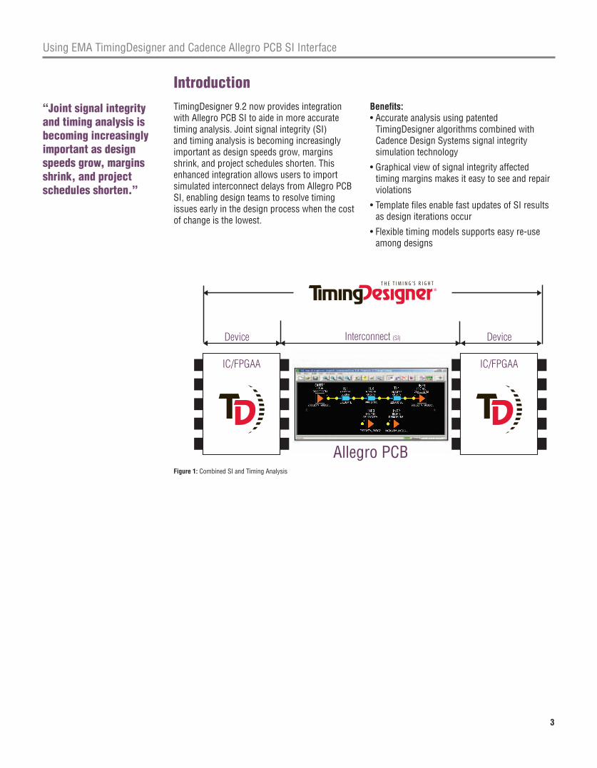
TimingDesigner9.2nowprovidesintegrationwithAllegroPCBSItoaideinmoreaccuratetiminganalysis.Jointsignalintegrity(SI)andtiminganalysisisbecomingincreasinglyimportantasdesignspeedsgrow,marginsshrink,andprojectschedulesshorten.ThisenhancedintegrationallowsuserstoimportsimulatedinterconnectdelaysfromAllegroPCBSI,enablingdesignteamstoresolvetimingissuesearlyinthedesignprocesswhenthecostofchangeisthelowest.
Benefits:•Accurateanalysisusingpatented
TimingDesigneralgorithmscombinedwithCadenceDesignSystemssignalintegritysimulationtechnology
•Graphicalviewofsignalintegrityaffectedtimingmarginsmakesiteasytoseeandrepairviolations
•TemplatefilesenablefastupdatesofSIresultsasdesigniterationsoccur
•Flexibletimingmodelssupportseasyre-useamongdesigns
Introduction
“Joint signal integrity and timing analysis is becoming increasingly important as design speeds grow, margins shrink, and project schedules shorten.”
Allegro PCB
Interconnect (SI) DeviceDevice
IC/FPGAAIC/FPGAAIC/FPGAA

UsingEMATimingDesignerandCadenceAllegroPCBSIInterface
From a text file of timing delaysAn Interactive Timing Diagram
To...
Figure 2:TableofValuestoGraphicalAnalysis
4
ThisapplicationnotebrieflydescribesthestepsinvolvedtoperformaninterfacetiminganalysisusingTimingDesignerandAllegroPCBSI.ThisinterfaceenablesthedesignteamtogivecontexttothesimulateddelayscalculatedinAllegroPCBSIandapplythemtoaninteractivetimingmodelfortimingmarginverification(Figure2).
Withoutthisinterface,theprocesstodeterminethetimingeffectsofPCBinterconnectdelayismanualanderrorprone,requiringcustomscriptsandcustomerdevelopedspreadsheets.TheintegrationbetweenAllegroPCBSIandTimingDesignerallowstheuseranautomatedtoolbasedprocesstovalidatedesigntimingearlyinthedesigncycle.
Design FlowThedesignflowhasbeenbuilttoprovidetheuserwithastreamlinedprocessforvalidatingdesigntiming.Theflowemploysinterfacetemplatestoallowforeasyre-importofSIanalysisfordesigniterationsorevenuseinsubsequentprojects.Thiswillsavetheengineeringteamtimeastheyrefinetheirdesignandavoiderrorsastheprocessensuresthesamesimulationscenarioisanalyzedeachtime(Figure3).
Overview
“The integration between Allegro PCB SI and TimingDesigner provides an automated tool based process to validate timing early in the design cycle.”
Figure 3:TimingDesignerAllegroPCBSIDesignFlow
1. Run SI simulations on target nets
2. Generate Standard Delay report
5. Re-Run SI simulation based on timing / design changes. Re-Import to validate in TimingDesigner.
6. TimingDesigner interconnect model and SI Template file saved off for re-use
3. Import Interconnect Delay into TimingDesigner
4. Perform timing analysis. If violations occur test repair options in TimingDesigner
PCB SI
UsingEMATimingDesignerandCadenceAllegroPCBSIInterface
5
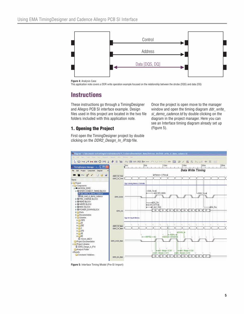
Figure 4:AnalysisCaseThisapplicationnotecoversaDDRwriteoperationexamplefocusedontherelationshipbetweenthestrobe(DQS)anddata(DQ)
Control
Address
Data [DQS, DQ]
Figure 5:InterfaceTimingModel(Pre-SIImport)
InstructionsTheseinstructionsgothroughaTimingDesignerandAllegroPCBSIinterfaceexample.Designfilesusedinthisprojectarelocatedinthetwofilefoldersincludedwiththisapplicationnote.
1. Opening the ProjectFirstopentheTimingDesignerprojectbydoubleclickingontheDDR2_Design_In_IP.tdpfile.
Oncetheprojectisopenmovetothemanagerwindowandopenthetimingdiagramddr_write_si_demo_cadence.tdbydoubleclickingonthediagramintheprojectmanager.HereyoucanseeanInterfacetimingdiagramalreadysetup(Figure5).
UsingEMATimingDesignerandCadenceAllegroPCBSIInterface
6
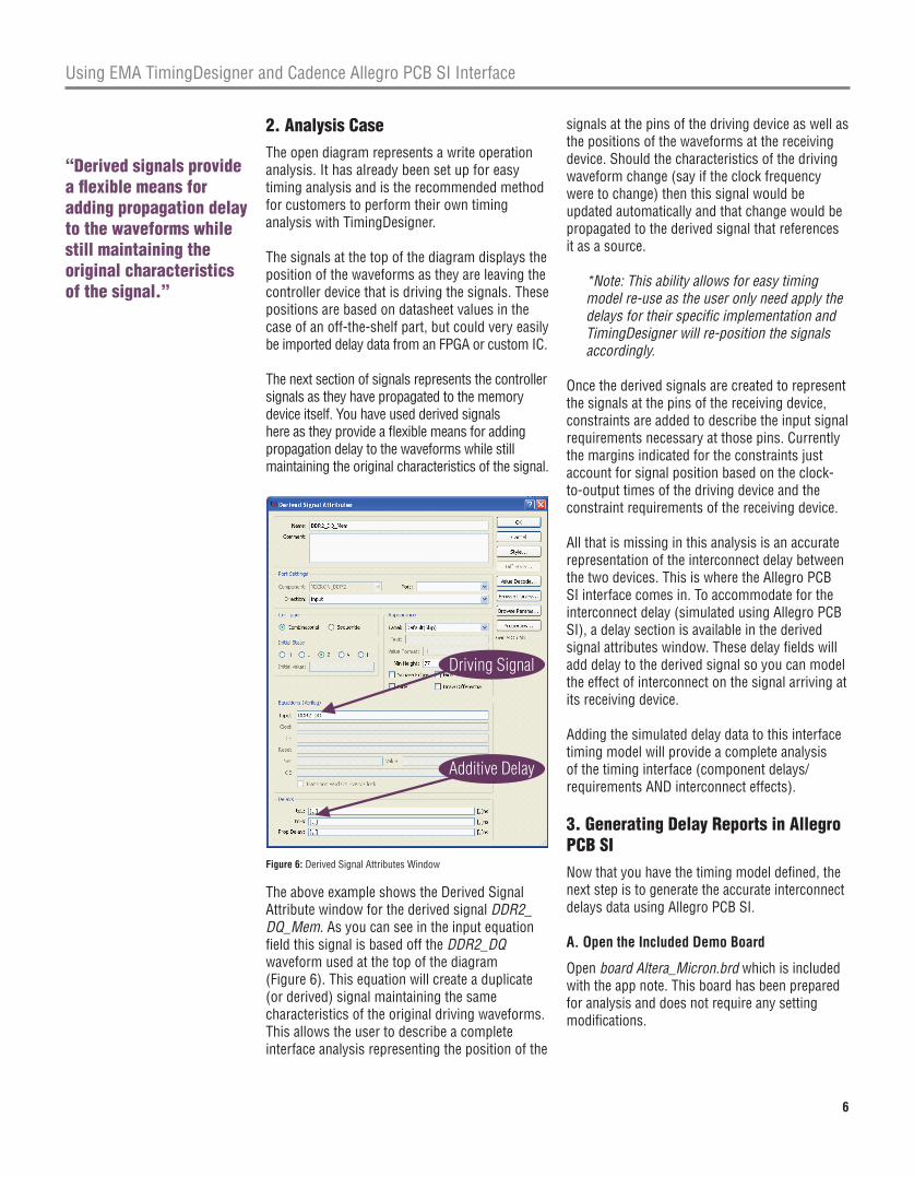
“Derived signals provide a flexible means for adding propagation delay to the waveforms while still maintaining the original characteristics of the signal.”
Figure 6:DerivedSignalAttributesWindow
Additive Delay
Driving Signal
2. Analysis CaseTheopendiagramrepresentsawriteoperationanalysis.IthasalreadybeensetupforeasytiminganalysisandistherecommendedmethodforcustomerstoperformtheirowntiminganalysiswithTimingDesigner.
Thesignalsatthetopofthediagramdisplaysthepositionofthewaveformsastheyareleavingthecontrollerdevicethatisdrivingthesignals.Thesepositionsarebasedondatasheetvaluesinthecaseofanoff-the-shelfpart,butcouldveryeasilybeimporteddelaydatafromanFPGAorcustomIC.
Thenextsectionofsignalsrepresentsthecontrollersignalsastheyhavepropagatedtothememorydeviceitself.Youhaveusedderivedsignalshereastheyprovideaflexiblemeansforaddingpropagationdelaytothewaveformswhilestillmaintainingtheoriginalcharacteristicsofthesignal.
TheaboveexampleshowstheDerivedSignalAttributewindowforthederivedsignalDDR2_DQ_Mem.AsyoucanseeintheinputequationfieldthissignalisbasedofftheDDR2_DQwaveformusedatthetopofthediagram(Figure6).Thisequationwillcreateaduplicate(orderived)signalmaintainingthesamecharacteristicsoftheoriginaldrivingwaveforms.Thisallowstheusertodescribeacompleteinterfaceanalysisrepresentingthepositionofthe
signalsatthepinsofthedrivingdeviceaswellasthepositionsofthewaveformsatthereceivingdevice.Shouldthecharacteristicsofthedrivingwaveformchange(sayiftheclockfrequencyweretochange)thenthissignalwouldbeupdatedautomaticallyandthatchangewouldbepropagatedtothederivedsignalthatreferencesitasasource.
*Note: This ability allows for easy timing model re-use as the user only need apply the delays for their specific implementation and TimingDesigner will re-position the signals accordingly.
Oncethederivedsignalsarecreatedtorepresentthesignalsatthepinsofthereceivingdevice,constraintsareaddedtodescribetheinputsignalrequirementsnecessaryatthosepins.Currentlythemarginsindicatedfortheconstraintsjustaccountforsignalpositionbasedontheclock-to-outputtimesofthedrivingdeviceandtheconstraintrequirementsofthereceivingdevice.
Allthatismissinginthisanalysisisanaccuraterepresentationoftheinterconnectdelaybetweenthetwodevices.ThisiswheretheAllegroPCBSIinterfacecomesin.Toaccommodatefortheinterconnectdelay(simulatedusingAllegroPCBSI),adelaysectionisavailableinthederivedsignalattributeswindow.Thesedelayfieldswilladddelaytothederivedsignalsoyoucanmodeltheeffectofinterconnectonthesignalarrivingatitsreceivingdevice.
Addingthesimulateddelaydatatothisinterfacetimingmodelwillprovideacompleteanalysisofthetiminginterface(componentdelays/requirementsANDinterconnecteffects).
3. Generating Delay Reports in Allegro PCB SINowthatyouhavethetimingmodeldefined,thenextstepistogeneratetheaccurateinterconnectdelaysdatausingAllegroPCBSI.
A. Open the Included Demo Board
Openboard Altera_Micron.brdwhichisincludedwiththeappnote.Thisboardhasbeenpreparedforanalysisanddoesnotrequireanysettingmodifications.

UsingEMATimingDesignerandCadenceAllegroPCBSIInterface
7
Figure 7:AllegroPCBSISignalAnalysisDialog
B. Run Simulation
Forthisexample,youarelookingatasinglebytelaneofoneoftheon-boardmemorydevices.Thissubsetofthefullmemoryinterfacewaschosentoreducethedatasetandallowfocusontheanalysisprocess.Theanalysisscopecanbeexpandedtocoverallaspectsoftheinterfaceasneeded.Torunthesimulationyouwillneedtodefinethenetstobesimulated.
Todothis,goto:
Analyze > SI / EMI Sim > Probe(thesignalanalysiswindowwillappear).Youwillwanttoaddthefollowingnetsforanalysis:
(DriverU13/ReceiverU28)DDR2_CK_NODDR2_DQS0DDR2_DQ0DDR2_DQ1DDR2_DQ2DDR2_DQ3DDR2_DQ4DDR2_DQ5DDR2_DQ6DDR2_DQ7
TheAllegroBoardfilefolderincludesaddr.lstfilewhichcanbeusedtoautomaticallypopulatethelistofnetsyouwanttosimulate.Usethelistofnetscommandtoselecttheddr2.lstfile(Figure7).
C. Generate Report
Oncethecorrectnetshavebeenselected,clickonreportstobringupthereportswindow(Figure8).
ThereporttogenerateforTimingDesigneristhedelayreport.OnlythisreportformatcanbeimportedusingtheAllegroPCBSI/TimingDesignerinterface.
AllsettingsbelowtheReport Typesectionarefreelyselectablebytheusertodefinethetypeofsimulationandresultsproducedforthereport.
*Note: It is recommended to at least choose Fast, Typical, and Slow as FST modes, as this will allow you to do a multi-mode analysis in TimingDesigner later on.
Oncethesettingshavebeenchosen,selectCreate ReporttogeneratethedelayreportandsaveitoffforimportintoTimingDesigner.
Figure 8:AllegroPCBSIReportDialog

UsingEMATimingDesignerandCadenceAllegroPCBSIInterface
8
Figure 9: TextReportfromAllegroPCBSI
D. Preview Generated Report (Optional)
Thegeneratedreportisatextfile(Figure9)whichcontainsdelaysinatabularformat.Thesefilesaredifficulttoreadorunderstandandprovidenocontextastowhatthesesimulateddelaysactuallymeantotheoperationofyourinterface.ImportingthesedelaysintoTimingDesignerallowsaneasilyvisiblewaytoreviewacompletetiminganalysisandseetheeffectsofinterconnectdelayonyourdevicerequirements.
4. Importing Data into TimingDesignerThebestplacetoimportthedelaydataisintoaTimingDesignerLibraryFile,asthisprovidesforeasywhat-ifanalysisusingTimingDesigner’sAliasingcapabilities(whichwillbedescribedlater).
Toimportthedelayfileyoujustcreatedinstep3,openanexistinglibraryfileorcreateanewlibrarythenselectFile > Import / Merge.IntheFiles of type:fieldselectAllegro PCB SI Delay File (*.txt)thenbrowsetothereportfileyoujust
created.Forthisexamplewe’veusedtheexistingProjectLibraryDDR2_Design_in_IP.tltoimportourdatawhichcanbeopenedthroughtheprojectmanagerwindow.Itisrecommendedyouusethesamelibrarytobesttakeadvantageofthealiasingstructureputtogetherinthediagram.
Note: Included with the TimingDesigner files are two sample reports that were pre-generated from the Allegro PCB SI tool. These reports are located in the TDSI_TD_DemoFiles > Docs folder of the demo package. The reports are:
• SI_Delay_write1_all_same_length.txt • SI_Delay_write2_longer_strobe.txt
The first report is an example of SI simulations of the board before any changes have been made, and the second is after SI and timing have been analyzed and design modifications made to fix errors. These can be used if access to the SI tool is not possible or convenient.
“TimingDesigner provides an easily visible way to review a complete timing analysis and see the effects of interconnect delay on your device requirements.”
UsingEMATimingDesignerandCadenceAllegroPCBSIInterface
9
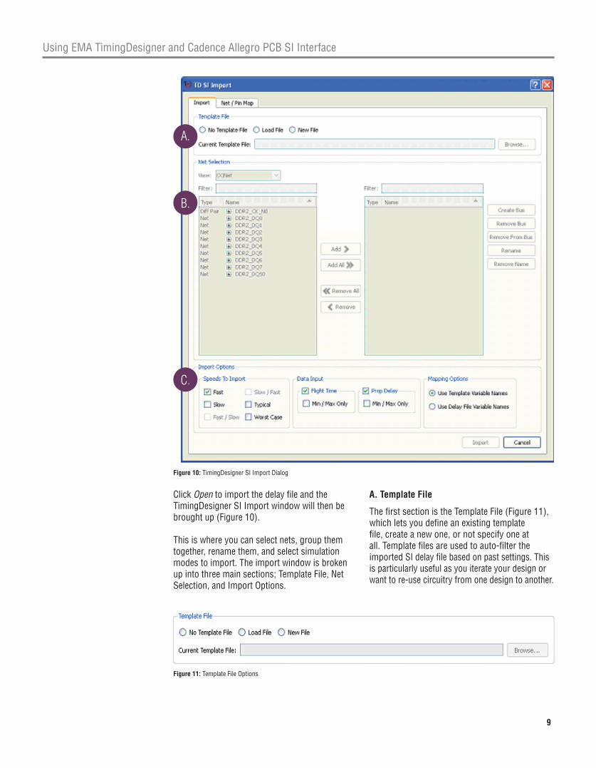
Figure 10: TimingDesignerSIImportDialog
A.
B.
C.
ClickOpentoimportthedelayfileandtheTimingDesignerSIImportwindowwillthenbebroughtup(Figure10).
Thisiswhereyoucanselectnets,groupthemtogether,renamethem,andselectsimulationmodestoimport.Theimportwindowisbrokenupintothreemainsections;TemplateFile,NetSelection,andImportOptions.
A. Template File
ThefirstsectionistheTemplateFile(Figure11),whichletsyoudefineanexistingtemplatefile,createanewone,ornotspecifyoneatall.Templatefilesareusedtoauto-filtertheimportedSIdelayfilebasedonpastsettings.Thisisparticularlyusefulasyouiterateyourdesignorwanttore-usecircuitryfromonedesigntoanother.
Figure 11:TemplateFileOptions
UsingEMATimingDesignerandCadenceAllegroPCBSIInterface
10
Atemplatefile(DDR2_Design_In_IP_Template.tf)isincludedwiththedemofilesprovidedtouseforquickimportofdata.Tousethetemplatefileselect‘loadfile’andthenbrowsetotheincludedtemplatefile.Oncethetemplatefileisloaded,click‘mport (Ifyouusethetemplatefileskiptosection5)
*Note: Just to get a feel for the import function you may want to browse through the net selection field and the various views you can use.
[Optional]Ifwanttogothroughanewinterfaceanalysis,belowarethestepstoselectnets,groupbuses,rename,nets,andimportdelays.
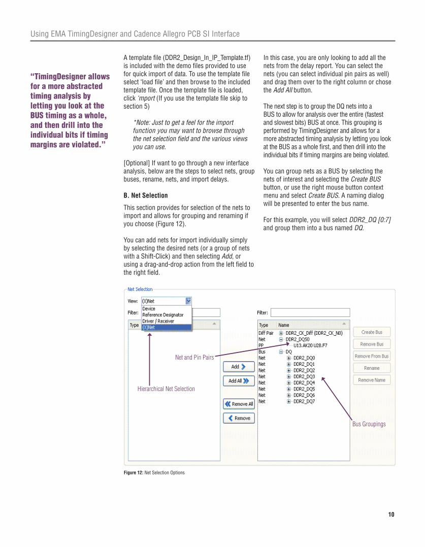
B. Net Selection
Thissectionprovidesforselectionofthenetstoimportandallowsforgroupingandrenamingifyouchoose(Figure12).
Youcanaddnetsforimportindividuallysimplybyselectingthedesirednets(oragroupofnetswithaShift-Click)andthenselecting Add,orusingadrag-and-dropactionfromtheleftfieldtotherightfield.
Inthiscase,youareonlylookingtoaddallthenetsfromthedelayreport.Youcanselectthenets(youcanselectindividualpinpairsaswell)anddragthemovertotherightcolumnorchosetheAdd Allbutton.
ThenextstepistogrouptheDQnetsintoaBUStoallowforanalysisovertheentire(fastestandslowestbits)BUSatonce.ThisgroupingisperformedbyTimingDesignerandallowsforamoreabstractedtiminganalysisbylettingyoulookattheBUSasawholefirst,andthendrillintotheindividualbitsiftimingmarginsarebeingviolated.
YoucangroupnetsasaBUSbyselectingthenetsofinterestandselectingtheCreate BUSbutton,orusetherightmousebuttoncontextmenuandselectCreate BUS.Anamingdialogwillbepresentedtoenterthebusname.
Forthisexample,youwillselectDDR2_DQ [0:7]andgroupthemintoabusnamed DQ.
Figure 12:NetSelectionOptions
Hierarchical Net Selection
Net and Pin Pairs
Bus Groupings
“TimingDesigner allows for a more abstracted timing analysis by letting you look at the BUS timing as a whole, and then drill into the individual bits if timing margins are violated.”
UsingEMATimingDesignerandCadenceAllegroPCBSIInterface
11
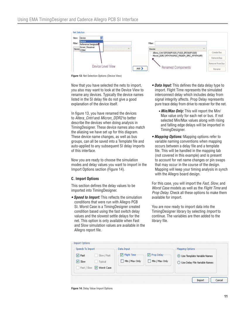
Figure 13:NetSelectionOptions(DeviceView)
Device Level View Renamed Components
Nowthatyouhaveselectedthenetstoimport,youalsomaywanttolookattheDeviceViewtorenameanydevices.TypicallythedevicenameslistedintheSIdelayfiledonotgiveagoodexplanationofthedeviceitself.
Infigure13,youhaverenamedthedevicestoAltera_CntrlandMicron_DDR2tobetterdescribethedeviceswhendoinganalysisinTimingDesigner.Thesedevicenamesalsomatchthealiasingwehavesetupforthisdiagram.Thesedevicenamechanges,aswellasbusgroups,canallbesavedintoaTemplatefileandauto-appliedtoanysubsequentSIdelayimportsofthisinterface.
NowyouarereadytochoosethesimulationmodesanddelayvaluesyouwanttoimportintheImportOptionssection(Figure14).
C. Import Options
ThissectiondefinesthedelayvaluestobeimportedintoTimingDesigner.
• Speed to Import:ThisreflectsthesimulationconditionsthatwererunwithAllegroPCBSI.WorstCaseisaTimingDesignercreatedconditionbasedusingthefastswitchdelayvaluesandtheslowestsettledelaysforthenet.ThisoptionisonlyavailablewhenFastandSlowsimulationvaluesareavailableintheAllegroreportfile.
• Data Input:Thisdefinesthedatadelaytypetoimport.FlightTimerepresentsthesimulatedinterconnectdelaywhichincludesdelayfromsignalintegrityaffects.PropDelayrepresentspuretracedelayfromdrivetoreceiverforthenet.
• Min/Max Only:ThiswillreporttheMin/Maxvalueonlyforeachnetorbus.IfnotselectedMin/MaxvaluesalongwithrisingandfallingedgedelayswillbeimportedinTimingDesigner.
• Mapping Options:Mappingoptionsrefertovariablenamingconventionswhenmappingoccursbetweenadelayfileandatemplatefile.Thiswillbehandledinthemappingtab(notcoveredinthisexample)andispresenttoaccountfornetnamechangesorpinswapsthatmayoccurinthecourseofthedesign.MappingwillkeepyourtiminganalysisinsynchwiththeAllegroboarddesign.
Forthiscase,youwillimporttheFast, Slow,andWorst CasemodelsaswellastheFlight TimeandProp Delay.Checkalltheseoptionstomakethemavailableforimport.
YouarenowreadytoimportdataintotheTimingDesignerlibrarybyselecting Importtocontinue.Thevariablesarethenaddedtothelibraryfile.
Figure 14:DelayValueImportOptions
UsingEMATimingDesignerandCadenceAllegroPCBSIInterface
12
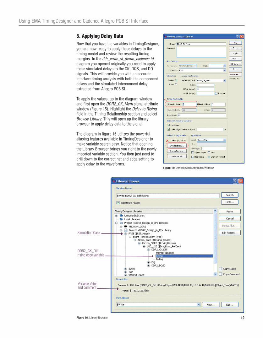
5. Applying Delay DataNowthatyouhavethevariablesinTimingDesigner,youarenowreadytoapplythesedelaystothetimingmodelandreviewtheresultingtimingmargins.Intheddr_write_si_demo_cadence.tddiagramyouopenedoriginallyyouneedtoapplythesesimulateddelaystotheCK,DQS,andDQsignals.ThiswillprovideyouwithanaccurateinterfacetiminganalysiswithboththecomponentdelaysandthesimulatedinterconnectdelayextractedfromAllegroPCBSI.
Toapplythevalues,gotothediagramwindowandfirstopentheDDR2_CK_Memsignalattributewindow(Figure15).HighlighttheDelay to RisingfieldintheTimingRelationshipsectionandselectBrowse Library.Thiswillopenupthelibrarybrowsertoapplydelaydatatothesignal.
Thediagraminfigure16utilizesthepowerfulaliasingfeaturesavailableinTimingDesignertomakevariablesearcheasy.NoticethatopeningtheLibraryBrowserbringsyourighttothenewlyimportedvariablesection.Youthenjustneedtodrilldowntothecorrectnetandedgesettingtoapplydelaytothewaveforms.
Figure 15:DerivedClockAttributesWindow
Simulation Case
DDR2_CK_Diff rising edge variable
Variable Value and comment
Figure 16:LibraryBrowser
UsingEMATimingDesignerandCadenceAllegroPCBSIInterface
13
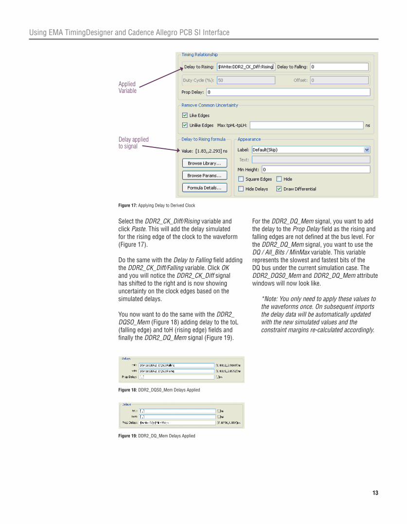
Applied Variable
Delay applied to signal
Figure 17:ApplyingDelaytoDerivedClock
SelecttheDDR2_CK_Diff/RisingvariableandclickPaste.Thiswilladdthedelaysimulatedfortherisingedgeoftheclocktothewaveform(Figure17).
DothesamewiththeDelay to FallingfieldaddingtheDDR2_CK_Diff/Fallingvariable.ClickOKandyouwillnoticetheDDR2_CK_Diffsignalhasshiftedtotherightandisnowshowinguncertaintyontheclockedgesbasedonthesimulateddelays.
YounowwanttodothesamewiththeDDR2_DQSO_Mem(Figure18)addingdelaytothetoL(fallingedge)andtoH(risingedge)fieldsandfinallytheDDR2_DQ_Mem signal (Figure19).
FortheDDR2_DQ_Memsignal,youwanttoaddthedelaytotheProp Delayfieldastherisingandfallingedgesarenotdefinedatthebuslevel.FortheDDR2_DQ_Memsignal,youwanttousetheDQ / All_Bits / MinMaxvariable.ThisvariablerepresentstheslowestandfastestbitsoftheDQbusunderthecurrentsimulationcase.TheDDR2_DQS0_MemandDDR2_DQ_Memattributewindowswillnowlooklike.
*Note: You only need to apply these values to the waveforms once. On subsequent imports the delay data will be automatically updated with the new simulated values and the constraint margins re-calculated accordingly.
Figure 18:DDR2_DQS0_MemDelaysApplied
Figure 19:DDR2_DQ_MemDelaysApplied
UsingEMATimingDesignerandCadenceAllegroPCBSIInterface
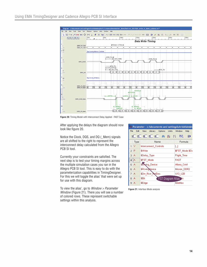
Afterapplyingthedelaysthediagramshouldnowlooklikefigure20.
NoticetheClock,DQS,andDQ(_Mem)signalsareallshiftedtotherighttorepresenttheinterconnectdelaycalculatedfromtheAllegroPCBSItool.
Currentlyyourconstraintsaresatisfied.ThenextstepistotestyourtimingmarginsacrossthemultiplesimulationcasesyouranintheAllegroPCBSItool.ThisiseasytodowiththeparameterizationcapabilitiesinTimingDesigner.Forthiswewilltogglethealias’thatweresetupforusewiththisdiagram.Toviewthealias’,gotoWindow > Parameter Window(Figure21).Thereyouwillseeanumberofcoloredrows.Theserepresentswitchablesettingswithinthisanalysis.
FST Diagram Alias
14
Figure 20:TimingModelwithInterconnectDelayApplied-FASTCase
Figure 21:InterfaceModeanalysis
UsingEMATimingDesignerandCadenceAllegroPCBSIInterface
15
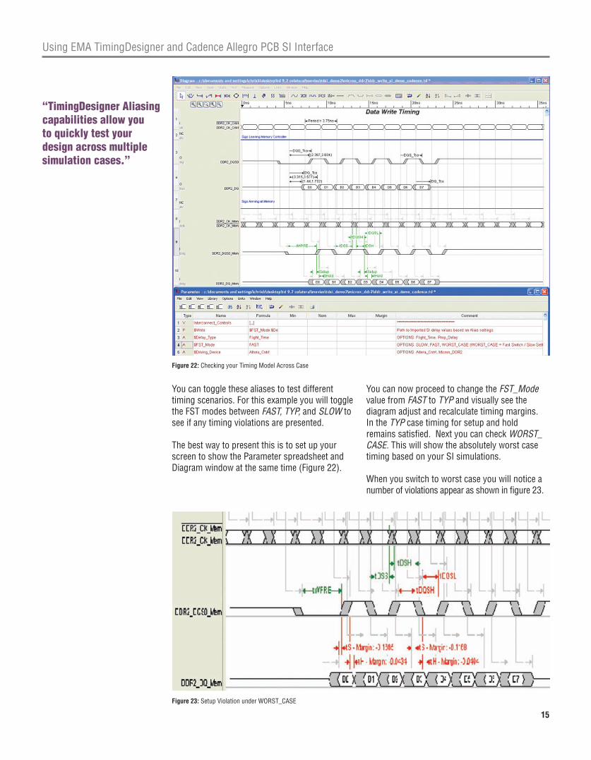
Youcantogglethesealiasestotestdifferenttimingscenarios.ForthisexampleyouwilltoggletheFSTmodesbetweenFAST, TYP,and SLOWtoseeifanytimingviolationsarepresented.
ThebestwaytopresentthisistosetupyourscreentoshowtheParameterspreadsheetandDiagramwindowatthesametime(Figure22).
YoucannowproceedtochangetheFST_ModevaluefromFASTtoTYPandvisuallyseethediagramadjustandrecalculatetimingmargins.IntheTYPcasetimingforsetupandholdremainssatisfied.NextyoucancheckWORST_CASE.ThiswillshowtheabsolutelyworstcasetimingbasedonyourSIsimulations.
Whenyouswitchtoworstcaseyouwillnoticeanumberofviolationsappearasshowninfigure23.
Figure 22:CheckingyourTimingModelAcrossCase
Figure 23:SetupViolationunderWORST_CASE
“TimingDesigner Aliasing capabilities allow you to quickly test your design across multiple simulation cases.”
UsingEMATimingDesignerandCadenceAllegroPCBSIInterface
16
6. Fixing ViolationsNowthatyouhaveidentifiedtimingviolations,thenextstepistotestdesignalternativestorepairthem.Youhaveanumberofoptionsheredependingonyourdesignrequirements.Inthisexamplewewilltalkabouttwo:Clockfrequencyandtracelength.
A. Changing your Clock Frequency
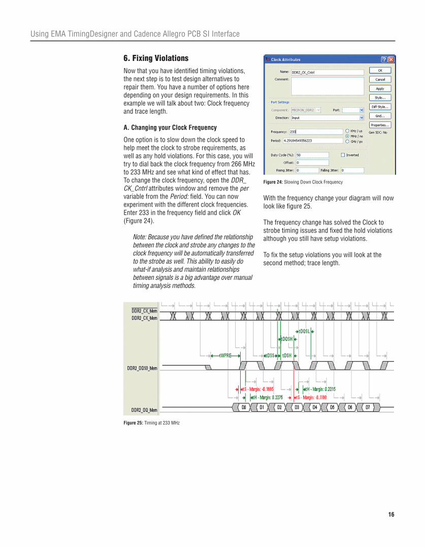
Oneoptionistoslowdowntheclockspeedtohelpmeettheclocktostroberequirements,aswellasanyholdviolations.Forthiscase,youwilltrytodialbacktheclockfrequencyfrom266MHzto233MHzandseewhatkindofeffectthathas.Tochangetheclockfrequency,opentheDDR_CK_CntrlattributeswindowandremovethepervariablefromthePeriod:field.Youcannowexperimentwiththedifferentclockfrequencies.Enter233inthefrequencyfieldandclickOK(Figure24).
Note: Because you have defined the relationship between the clock and strobe any changes to the clock frequency will be automatically transferred to the strobe as well. This ability to easily dowhat-if analysis and maintain relationships between signals is a big advantage over manual timing analysis methods.
Withthefrequencychangeyourdiagramwillnowlooklikefigure25.
ThefrequencychangehassolvedtheClocktostrobetimingissuesandfixedtheholdviolationsalthoughyoustillhavesetupviolations.
Tofixthesetupviolationsyouwilllookatthesecondmethod;tracelength.
Figure 24: SlowingDownClockFrequency
Figure 25: Timingat233MHz

UsingEMATimingDesignerandCadenceAllegroPCBSIInterface
B. Changing Trace Lengths
Modifyingyourtracelengthisagoodwaytorepairtimingviolations.Inthiscase,youaremissingoursetuprequirementsonboththerisingandfallingedgesofthestrobe.HereyouhavetheoptiontoeithermodifytheroutingfortheStrobeortheDQbus.Sincere-routingonetraceasopposedtotheentirebusistypicallyeasier,youwillfocusonmodifyingtheStrobesignal.
Lookingatoursetupandholdmargins,ifyoucanadd.2nsoftracedelaytotheStrobesignalyoushouldthenbeabletomeetbothsetupandholdconditionsinourworstcaseanalysis.YoucantestthisbyopeningtheDDR2_DQS0_Memsignalandadding.2totherisingandfallingfields(Figure26).
Yourdiagramwillnowlookfigure27.
Figure 26: IncreasingStrobeTraceDelay
Figure27:WriteDiagramwith2nsTestDelayAddedtoStrobe
17

UsingEMATimingDesignerandCadenceAllegroPCBSIInterface
18
Noticeallconstraintsarenowbeingmet.HavingvalidatedthetiminginTimingDesigner,nextyouwillneedtore-routetheStrobetomatchthenewlengthrequirements.IfyouhaveCadenceAllegroPCBPerformanceOptionorhigheryoucanusetheConstraintManagertorevisetherulesfortheStrobesignal.
Note: If you do not have Allegro PCB Performance Option or higher you will need to convert the .2ns into MILS. On average, a trace travels 6 inches in 1 ns so; 0.2ns would be 1.2 inches (1200 mils). To match the conditions in the timing diagram, 1200 mils of length needs to be added to the Strobe signal. You can then manually tune the trace to reach the new desired length.
ForthisexampleyouwillbeshownhowtoupdateConstraintManagerusingthenewroutingrulesfortheStrobesignal.
InAllegroXL,opentheConstraintManagerintheAltera_Micron.brdandgototheElectrical Tab > Net section > Relative Propagation DelayandfindtheMatchGroupcalledMG_DDR2_DQ_LANE0whereyouwillseetheexistingrule(Figure28).
TherulethatistherepresentlyhasallthebusbitsandtheStrobenetwiththesameexactlength(within50mils),butnowwewouldliketochangethattohavetheStrobenetbe1200mils(or0.2ns)longer.Itwilllooklikefigure29.
Figure 28: ConstraintManager
Figure 29: ConstraintManager;NewStrobeRuleApplied
“Cadence constraint manager allows you to easily apply and review rules for your design.”
UsingEMATimingDesignerandCadenceAllegroPCBSIInterface
19
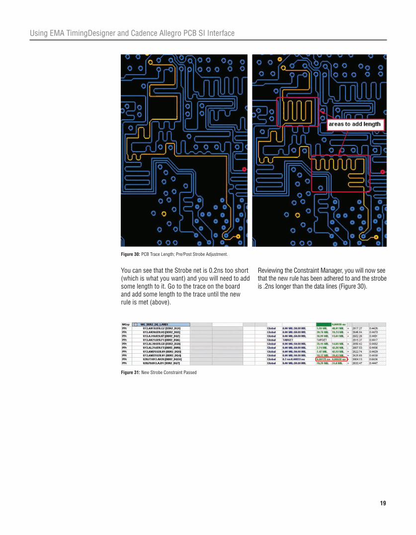
YoucanseethattheStrobenetis0.2nstooshort(whichiswhatyouwant)andyouwillneedtoaddsomelengthtoit.Gotothetraceontheboardandaddsomelengthtothetraceuntilthenewruleismet(above).
ReviewingtheConstraintManager,youwillnowseethatthenewrulehasbeenadheredtoandthestrobeis.2nslongerthanthedatalines(Figure30).
Figure 31: NewStrobeConstraintPassed
Figure 30: PCBTraceLength;Pre/PostStrobeAdjustment.

UsingEMATimingDesignerandCadenceAllegroPCBSIInterface
Figure 32: NewSimulatedDelaysAppliedtoTimingDesigner
20
ConclusionThismethodologyprovidesuserswithaneasy,graphicalsolutiontovalidatetimingacrosscaseusingsimulation-accuratedelayvaluestoaccountforinterconnecttiming.ThishelpsusersclosetheloopbetweenSIandtiminganalysis.Ifviolationsdooccur,TimingDesignerprovidesawhat-ifanalysisenvironmenttotestpotentialfixesfortheviolations.
InterfacetimingdiagramsdevelopedinTimingDesigner,aswellasthetemplatefilesforSIdelayimport,canbere-usedacrossnumerousdesignstoprovideanefficientre-usemethodologygoingforwardtoleveragepastsimulationandsetupworkinfutureprojects.ThetimingdiagramsdevelopedinTimingDesignerareeasilyincorporatedinprojectdocumentationeffortssavingsignificanttimedocumentingyourdesignanditsassociatedintellectualproperty.
Nowthatyouhaveadded.2nstothetrace,youwillwanttore-runthesimulationinAllegroPCBSIandre-importthetimingintoTimingDesignerforfinalvalidation.
SinceyouhavesavedourSIimportconfigurationsinatemplatefile,anyre-simulationsareeasytoimportandthetimingmarginsre-calculatedbyTimingDesigner.
ImportingthenewsimulateddelaysovertheoriginalsinourProjectlibrary,younowshowallmarginsbeingmet(Figure31).
Note: Remember to remove the .2ns test delay you added to the DQS signal, as this is now included in the delay value imported form Allegro PCB SI.
“TimingDesigner and Cadence PCB SI provide an easy to use methodology to close the look between SI and timing analysis.”
UsingEMATimingDesignerandCadenceAllegroPCBSIInterface
21
EXTRA - Reading TimeAreadtimingdiagram(ddr_read_si_demo_cadence.td)isalsoincludedintheTimingDesignerexampleproject.TheprocessisthesametodoareadanalysisusingthedelayssimulatedfromAllegroPCBSI.Togeneratethereadtimingsimulationvalues,somemodificationtothemodelsusedneedstobemade.Belowdescribesthechangesrequiredtomodelareadoperation.
TheDDR2_CK_*0netsarethedifferentialclocknetsandtheycanhavethesamemodelsforboththereadandwriteoperation.However,theothernetswillneeddifferentmodelsdependingonwhichoperation(Read/Write)isbeingperformed.
IntheWritemode(currentmodethatthe.brdfileisin),theU13(driverside)isusingtheCDSDefaultOutput_2p5vmodelandtheU28(receiverside)isusingtheU27_800_DQ_FULL_800model.ToswitchthistoReadmode,youneedtochangetheU13toareceiver(youwillusetheCDSDefaultInput_2p5vmodel)andyouwillchangetheU28tothedriver(usingtheCDSDefaultIO_2p5vmodel).
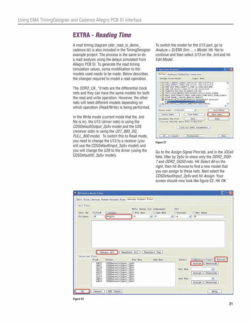
ToswitchthemodelfortheU13part,gotoAnalyze > SI/EMI Sim… > Model. HitYestocontinueandthenselect U13onthe.brdandhitEdit Model.
GototheAssign Signal Pinstab,andintheIOCellfield,filterby2p5vtoshowonlytheDDR2_DQ0-7andDDR2_DQS0nets.HitSelect Allontheright,thenhitBrowsetofindanewmodelthatyoucanassigntothesenets.NextselecttheCDSDefaultInput_2p5vandhitAssign.YourscreenshouldnowlooklikefigureE2.HitOK.
Figure E1
Figure E2
UsingEMATimingDesignerandCadenceAllegroPCBSIInterface
22
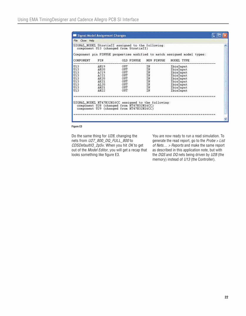
DothesamethingforU28,changingthenetsfromU27_800_DQ_FULL_800toCDSDefaultIO_2p5v.WhenyouhitOKtogetoutoftheModel Editor,youwillgetarecapthatlookssomethinglikefigureE3.
Youarenowreadytorunareadsimulation.Togeneratethereadreport,gototheProbe > List of Nets… > Reportsandmakethesamereportasdescribedinthisapplicationnote,butwiththeDQSandDQnetsbeingdrivenbyU28(thememory)insteadofU13(theController).
Figure E3
UsingEMATimingDesignerandCadenceAllegroPCBSIInterface
©2010EMADesignAutomation,Inc.AllrightsreservedintheU.S.andothercountries.EMADesignAutomation,TimingDesignerandtheEMAlogoareregisteredtrademarksofEMADesignAutomation,Inc.Allothermarksarethepropertyoftheirrespectiveowners.
Where to Go for Help
Support
EMADesignAutomationiscommittedtoprovidingunsurpassedcustomerserviceandsupport.OursupportsiteincludesanextensiveportfolioofTimingDesignerinformationtokeepyouproductive.
Youcangetaccesstoproductdownloads,asearchableknowledgebase,onlinetutorials,traininginformation,FAQs,usermanuals,andmore.Pleasevisitourwebsitehttp://support.ema-eda.com/toaccessthismaterialandmoredetailedinformation.
Support Contact Information
TechnicalSupport.........................................................................................techsupport@ema-eda.com
LicenseInformation..............................................................................................update@ema-eda.com
Phone(withinNorthAmerica)............................................................................................800.813.7494
Phone(outsideNorthAmerica)..........................................................................................585.334.6001
Fax......................................................................................................................................585.334.6693
General Contact Information
EMAWebsite..............................................................................................................www.ema-eda.com
TimingDesignerWebsite..................................................................................www.timingdesigner.com
InformationandSales................................................................................................info@ema-eda.com
EmploymentOpportunities................................................................................resumes@ema-eda.com