Embed Size (px)
DESCRIPTION
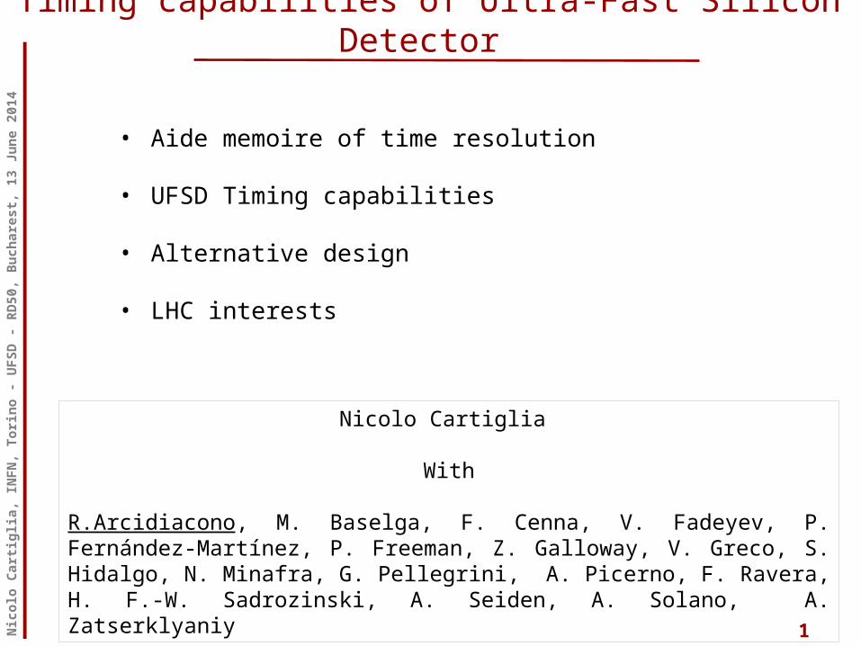
Timing capabilities of Ultra-Fast Silicon Detector. Aide memoire of time resolution UFSD Timing capabilities Alternative design LHC interests. Nicolo Cartiglia With - PowerPoint PPT Presentation
Citation preview
Nic
olo
Cart
iglia
, IN
FN, T
orin
o - U
FSD
- RD
50, B
ucha
rest
, 13
June
201
4
Timing capabilities of Ultra-Fast Silicon Detector
1
• Aide memoire of time resolution
• UFSD Timing capabilities
• Alternative design
• LHC interests
Nicolo Cartiglia
With
R.Arcidiacono, M. Baselga, F. Cenna, V. Fadeyev, P. Fernández-Martínez, P. Freeman, Z. Galloway, V. Greco, S. Hidalgo, N. Minafra, G. Pellegrini, A. Picerno, F. Ravera, H. F.-W. Sadrozinski, A. Seiden, A. Solano, A. Zatserklyaniy
Nic
olo
Cart
iglia
, IN
FN, T
orin
o - U
FSD
- RD
50, B
ucha
rest
, 13
June
201
4
2
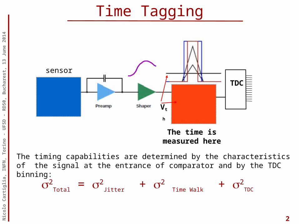
Time Tagging
s2Total = s2
Jitter + s2 Time Walk + s2TDC
The timing capabilities are determined by the characteristics of the signal at the entrance of comparator and by the TDC binning:
sensor
The time is measured here
Vt
h
TDC
Nic
olo
Cart
iglia
, IN
FN, T
orin
o - U
FSD
- RD
50, B
ucha
rest
, 13
June
201
4
3
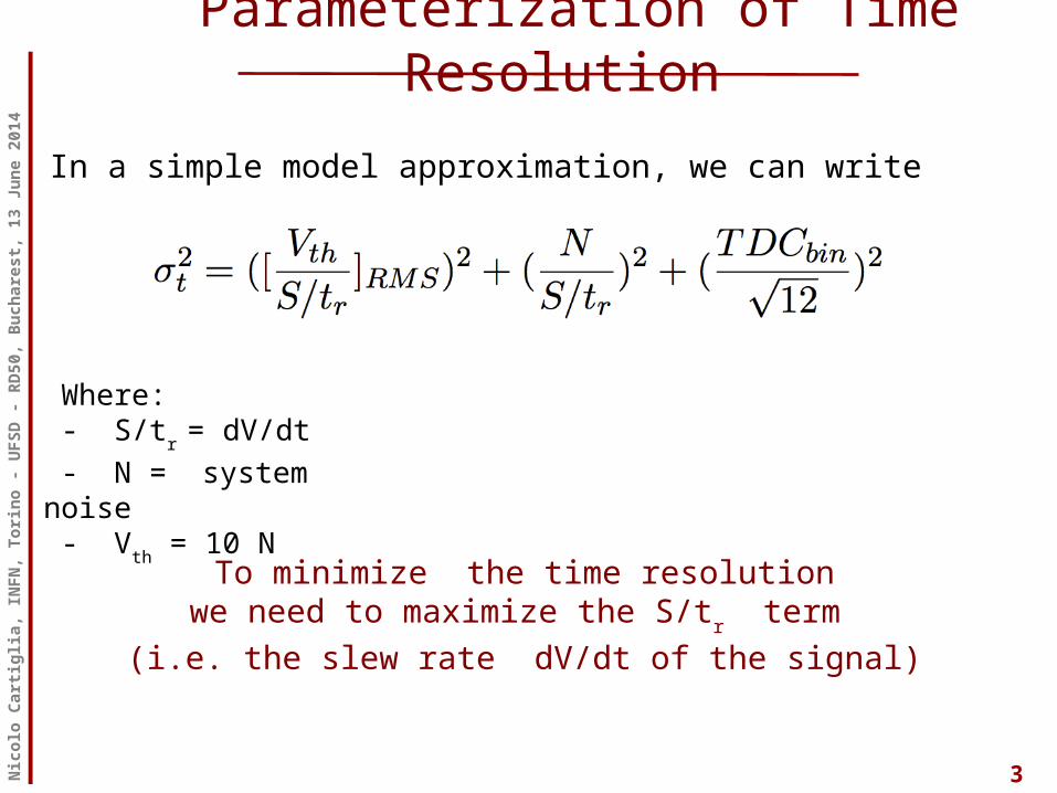
Parameterization of Time Resolution
To minimize the time resolution we need to maximize the S/tr term
(i.e. the slew rate dV/dt of the signal)
Where: - S/tr = dV/dt - N = system noise - Vth = 10 N
In a simple model approximation, we can write
Nic
olo
Cart
iglia
, IN
FN, T
orin
o - U
FSD
- RD
50, B
ucha
rest
, 13
June
201
4
4
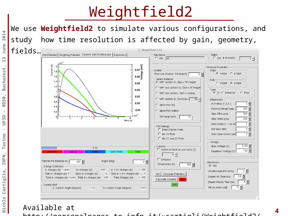
Weightfield2We use Weightfield2 to simulate various configurations, and study how time resolution is affected by gain, geometry, fields…
Available at http://personalpages.to.infn.it/~cartigli/Weightfield2/
Nic
olo
Cart
iglia
, IN
FN, T
orin
o - U
FSD
- RD
50, B
ucha
rest
, 13
June
201
4
5
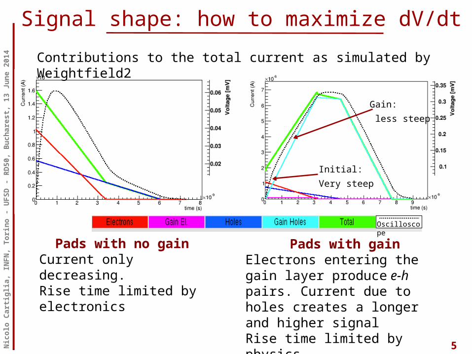
Signal shape: how to maximize dV/dt
Pads with gainElectrons entering the gain layer produce e-h pairs. Current due to holes creates a longer and higher signalRise time limited by physics
2 sensorsPads with no gain
Current only decreasing.Rise time limited by electronics
Contributions to the total current as simulated by Weightfield2
Oscilloscope
Gain: less steep
Initial:Very steep
Nic
olo
Cart
iglia
, IN
FN, T
orin
o - U
FSD
- RD
50, B
ucha
rest
, 13
June
201
4
6
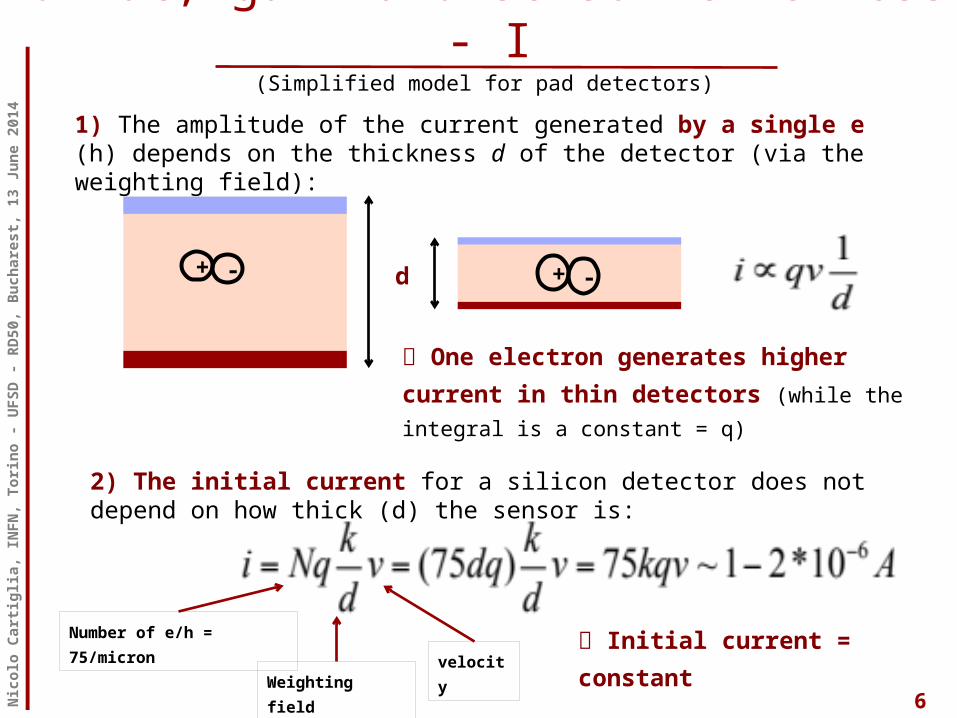
dV/dt, gain and sensor thickness - I1) The amplitude of the current generated by a single e (h) depends on the thickness d of the detector (via the weighting field):
+ - + -d
One electron generates higher current in thin detectors (while the integral is a constant = q)
Number of e/h = 75/micron
Weighting fieldvelocity
2) The initial current for a silicon detector does not depend on how thick (d) the sensor is:
Initial current = constant
(Simplified model for pad detectors)
Nic
olo
Cart
iglia
, IN
FN, T
orin
o - U
FSD
- RD
50, B
ucha
rest
, 13
June
201
4
7
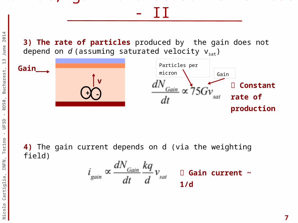
dV/dt, gain and sensor thickness - II3) The rate of particles produced by the gain does not depend on d (assuming saturated velocity vsat)
Particles per micron Gain
+ -v
Gain
Constant rate of production
Gain current ~ 1/d
4) The gain current depends on d (via the weighting field)
Nic
olo
Cart
iglia
, IN
FN, T
orin
o - U
FSD
- RD
50, B
ucha
rest
, 13
June
201
4
8
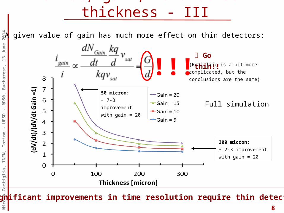
dV/dt, gain, and sensor thickness - III
!!!5) A given value of gain has much more effect on thin detectors:
Go thin!!(Real life is a bit more complicated, but the conclusions are the same)
300 micron:~ 2-3 improvement with gain = 20
50 micron:~ 7-8 improvement with gain = 20
Full simulation
Significant improvements in time resolution require thin detectors
Nic
olo
Cart
iglia
, IN
FN, T
orin
o - U
FSD
- RD
50, B
ucha
rest
, 13
June
201
4
9
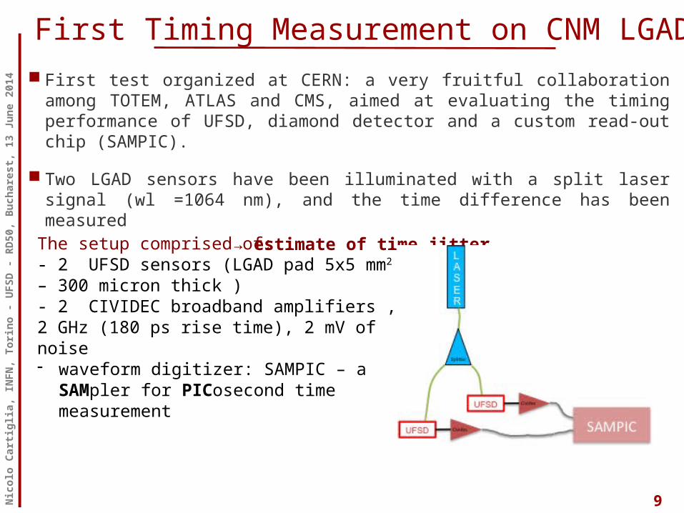
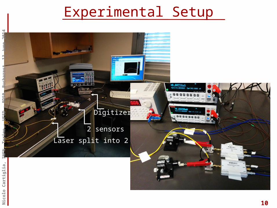
First Timing Measurement on CNM LGAD First test organized at CERN: a very fruitful collaboration among TOTEM,
ATLAS and CMS, aimed at evaluating the timing performance of UFSD, diamond detector and a custom read-out chip (SAMPIC).
Two LGAD sensors have been illuminated with a split laser signal (wl =1064 nm), and the time difference has been measured
→ estimate of time jitter
The setup comprised of: - 2 UFSD sensors (LGAD pad 5x5 mm2 – 300 micron thick ) - 2 CIVIDEC broadband amplifiers , 2 GHz (180 ps rise time), 2 mV of noise- waveform digitizer: SAMPIC – a
SAMpler for PICosecond time measurement
Nic
olo
Cart
iglia
, IN
FN, T
orin
o - U
FSD
- RD
50, B
ucha
rest
, 13
June
201
4
10
Experimental Setup
Digitizer
2 sensorsLaser split into 2
Nic
olo
Cart
iglia
, IN
FN, T
orin
o - U
FSD
- RD
50, B
ucha
rest
, 13
June
201
4
11
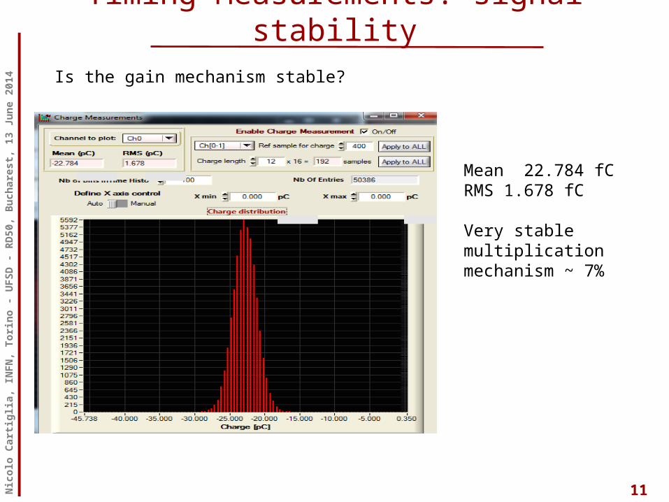
Timing Measurements: signal stability
Digitizer
2 sensorsLaser split into 2
Mean 22.784 fCRMS 1.678 fC
Very stable multiplication mechanism ~ 7%
Is the gain mechanism stable?
Nic
olo
Cart
iglia
, IN
FN, T
orin
o - U
FSD
- RD
50, B
ucha
rest
, 13
June
201
4
12
Digitizer
2 sensorsLaser split into 2
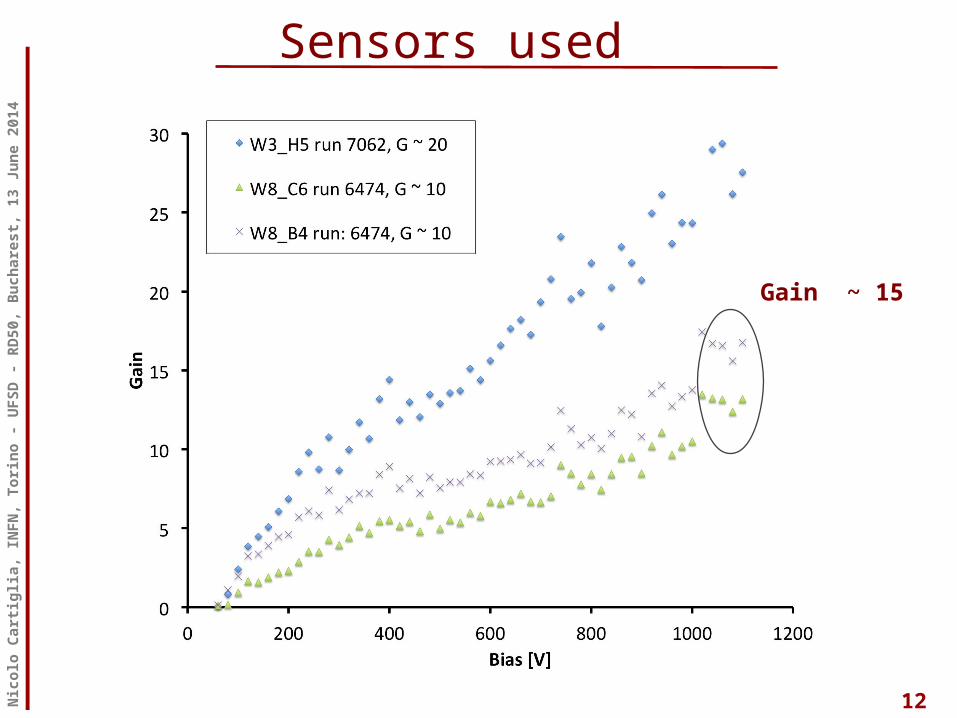
Sensors used
Gain ~ 15
Nic
olo
Cart
iglia
, IN
FN, T
orin
o - U
FSD
- RD
50, B
ucha
rest
, 13
June
201
4
13
Digitizer
2 sensorsLaser split into 2
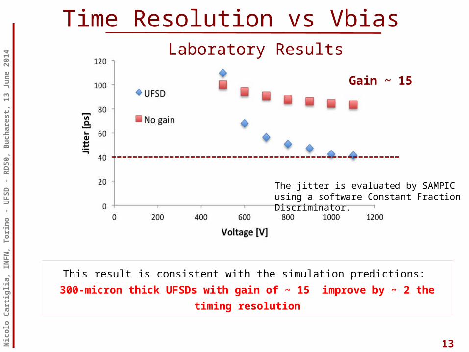
Time Resolution vs VbiasLaboratory Results
Gain ~ 15
The jitter is evaluated by SAMPIC using a software Constant Fraction Discriminator.
This result is consistent with the simulation predictions: 300-micron thick UFSDs with gain of ~ 15 improve by ~ 2 the
timing resolution
Nic
olo
Cart
iglia
, IN
FN, T
orin
o - U
FSD
- RD
50, B
ucha
rest
, 13
June
201
4
14
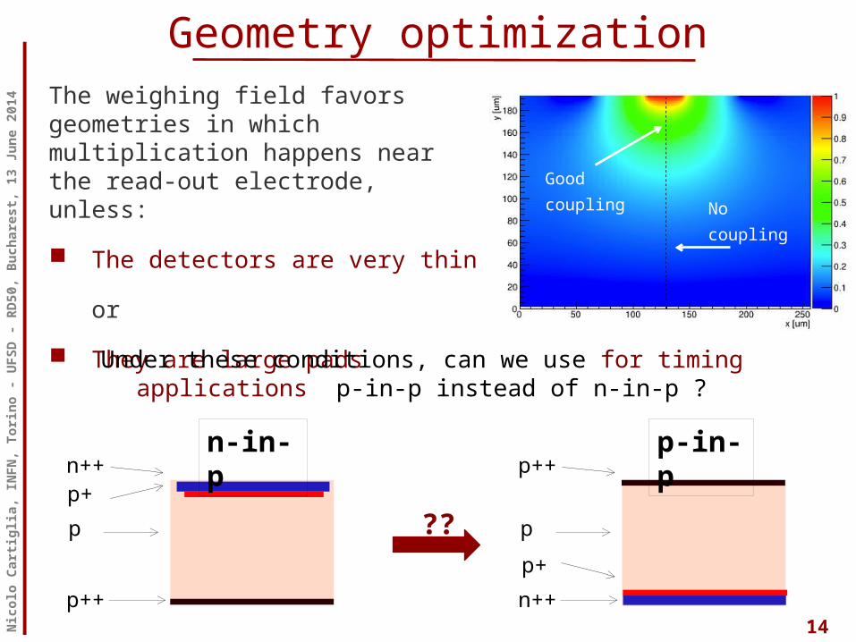
Geometry optimizationThe weighing field favors geometries in which multiplication happens near the read-out electrode, unless: The detectors are very thin
or They are large pads
Good coupling No
coupling
n++p+p
p++
n-in-p p++
p+p
n++
p-in-p
Under these conditions, can we use for timing applications p-in-p instead of n-in-p ?
??
Nic
olo
Cart
iglia
, IN
FN, T
orin
o - U
FSD
- RD
50, B
ucha
rest
, 13
June
201
4
15
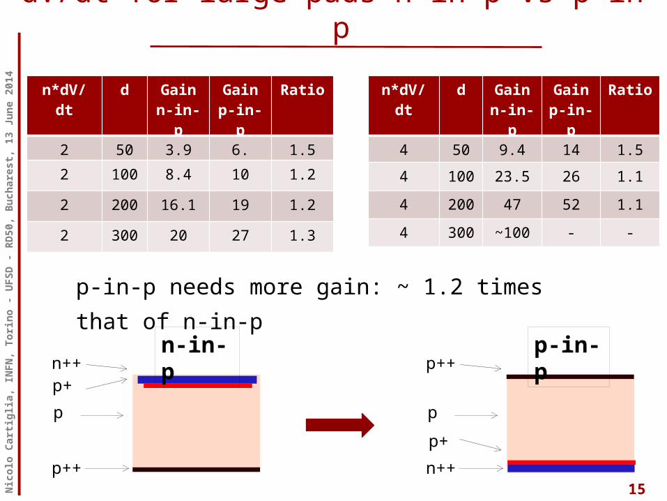
dV/dt for large pads n-in-p vs p-in-p
n++p+p
p++
n-in-p p++
p+p
n++
p-in-p
p-in-p needs more gain: ~ 1.2 times that of n-in-p
n*dV/dt
d Gain n-in-
p
Gain p-in-
p
Ratio
2 50 3.9 6. 1.52 100 8.4 10 1.22 200 16.1 19 1.22 300 20 27 1.3
n*dV/dt
d Gainn-in-
p
Gain p-in-
p
Ratio
4 50 9.4 14 1.54 100 23.5 26 1.14 200 47 52 1.14 300 ~100 - -
Nic
olo
Cart
iglia
, IN
FN, T
orin
o - U
FSD
- RD
50, B
ucha
rest
, 13
June
201
4
16
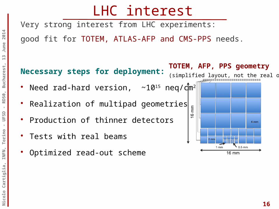
LHC interestVery strong interest from LHC experiments: good fit for TOTEM, ATLAS-AFP and CMS-PPS needs.
Necessary steps for deployment: Need rad-hard version, ~1015 neq/cm2
Realization of multipad geometries Production of thinner detectors Tests with real beams Optimized read-out scheme
TOTEM, AFP, PPS geometry(simplified layout, not the real one)
Nic
olo
Cart
iglia
, IN
FN, T
orin
o - U
FSD
- RD
50, B
ucha
rest
, 13
June
201
4
17
Summary We measured a jitter of 40 ps for a 300-micron thick pad
LGAD detectors Extrapolations indicate that a resolution of ~ 20 ps can be
achieved: thin detectors require much smaller gainA breakthrough in timing capabilities requires
thicknesses ~< 100 micron p-in-p design needs 20-30% higher gain Testbeams:
Now @ PSI end of July (PS) October (SPS) Requested Micro Ion Beam at Legnaro, (step of 1 micron)
Nic
olo
Cart
iglia
, IN
FN, T
orin
o - U
FSD
- RD
50, B
ucha
rest
, 13
June
201
4
18
This research was carried out with the contribution of the Ministero degli Affari Esteri, “Direzione Generale per la Promozione del Sistema Paese” of Italy.
This work was developed in the framework of the CERN RD50 collaboration and partially financed by the Spanish Ministry of Education and Science through the Particle Physics National Program (F P A2010−22060−C 02−02 and FPA2010 − 22163 − C02 − 02).
The work at SCIPP was partially supported by the United States Department of Energy, grant DE-FG02-04ER41286.
Acknowledgement
Nic
olo
Cart
iglia
, IN
FN, T
orin
o - U
FSD
- RD
50, B
ucha
rest
, 13
June
201
4
19
Backup
Nic
olo
Cart
iglia
, IN
FN, T
orin
o - U
FSD
- RD
50, B
ucha
rest
, 13
June
201
4
20
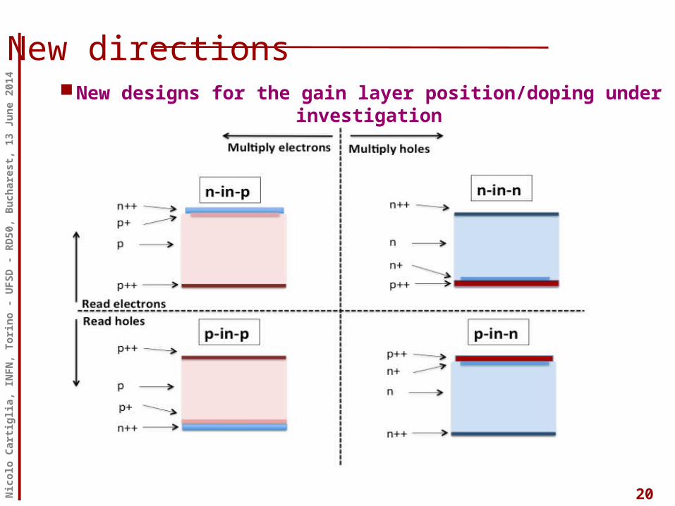
New directionsNew designs for the gain layer position/doping under
investigation
Nic
olo
Cart
iglia
, IN
FN, T
orin
o - U
FSD
- RD
50, B
ucha
rest
, 13
June
201
4
21
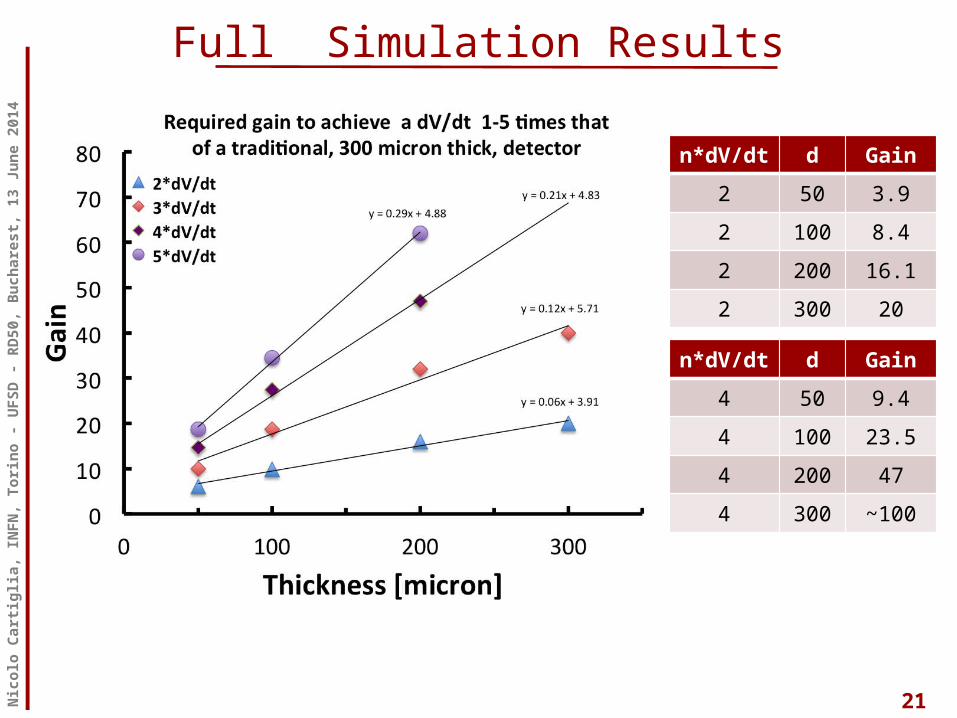
Full Simulation Results
n*dV/dt
d Gain
4 50 9.44 100 23.54 200 474 300 ~100
n*dV/dt
d Gain
2 50 3.92 100 8.42 200 16.12 300 20
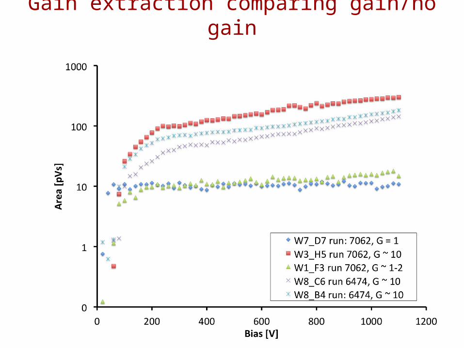
Gain extraction comparing gain/no gain22