Embed Size (px)
DESCRIPTION
Packet Network TIMING ISSUESCES over packet technologies emulate T1, E1, and other services by encapsulating TDM traffic into packets for transport across the packet switched network (PSN) and restoring the TDM traffic at the egress.
Citation preview

Timing and Sync over PSN
Tuan Nguyen-viet

OVERVIEWPart 1
Packet Network TIMING ISSUES
• CES over packet technologies emulate T1, E1, and other services by encapsulating TDM traffic into packets for transport across the packet switched network (PSN) and restoring the TDM traffic at the egress.
– At first glance it's not difficult to deliver TDM data over IP networks.– The challenge arises in the critical nature of timing and synchronization.
• Conventional circuit switched networks inherently distribute timing throughout the network based on very accurate primary reference clocks (PRCs).
– Building integrated timing supplies (BITS) in each central office distribute and stabilize the digital heartbeat that keeps each switch in sync.
– However PSNs do not have a timing structure. By its very nature the Ethernet is non-deterministic, which creates problems for time-sensitive applications (e.g., CES)that require precise synchronization.
– The PSN imposes delay and delay variation to packets that traverse the network.– In order for T1, E1 and wireless backhaul CES to reliably operate, synchronization is
needed at the end points of the service to remove the packet delay variation (PDV).
Challenging TIMING REQUIREMENTS
• T1 standards specify a maximum time interval error for the customer interface, measuring the maximum time variation of the clock at the transport level of 8.4 µs over 900 seconds and 18µs over 24 hours.
– The maximum time interval error at the synchronization level is 1 µs over 2,000 seconds and 2 µs over 100,000 seconds.
Challenging TIMING REQUIREMENTS (2)
• Mobile base stations have equally critical timing requirements. A frequency accuracy of ±50 parts per billion (ppb) is needed to achieve successful handoffs and maintain voice and data services.
• When the handoff between two base stations occurs, the mobile phone must rapidly switch from the frequency and/or time of the current base station to the target of the new base station.
– If a mobile phone is unable to react quickly enough to synchronization errors between base stations, the result will be a dropped call.
• Most GSM base stations (BTS’s) deployed today recover their synchronization from the TDM network delivered T1 or E1 service.
– If the T1 or E1 is delivered by CES then the packet network must be enhanced to include synchronization.
– Similarly if the base station uses native IP backhaul where CES encapsulation is not needed, there is still a need to provide synchronization for the base station frequency.
Timing and SYNCHRONIZATION METHODS
• Adaptive Clock Recovery (ACR) is a best effort method utilized today to provide timing and synchronization for CES over PSN applications.
• This method relies upon the fact that the source is producing bits at a constant rate determined by its clock.
• When the bits arrive at the destination, they are separated by a random component know as packet delay variation (PDV).
• Adaptive clock recovery involves averaging these bits in order to even out their gaps and negate the effects of PDV.
• The weakness of ACR is that it requires an expensive oscillator at the source, and field performance is uncertain under exposure to high levels of PDV present in live networks.
Timing and SYNCHRONIZATION METHODS (2)
• An alternative to ACR is to install a GPS receiver at each base station and use it as a stable clock reference for re-timing the CES packets between the CES modem and the base station T1/E1 input.
• The timing signal received by the base station is retimed to be precise and stable.• The disadvantage of GPS-based retimers is that they involve a substantial cost and
implementation burden.– First, there is the need to equip each base station with a GPS receiver, involving a
significant capital cost.– With several million base stations in the world, the required investment is substantial.– Another concern is that the existing GPS may not be an acceptable solution for all sites
since GPS signals may be weak indoors or in metropolitan areas.– Moreover, some wireless operators internationally may not want to use a GPS signal
controlled by the United States.
Timing and SYNCHRONIZATION METHODS (3)
• Another alternative is to integrate GPS directly into the base station equipment or deploy stand-alone rubidium clocks.
• Rubidium based oscillators provide a highly robust solution that has been proven to meet the 50 ppb requirement over the full service life of the equipment.
• Quartz oscillators, on the other hand, are subject to higher native aging rates and warm-up/restabilization characteristics that make it difficult to assure compliance to the 50 ppb requirement for more than six to 12 months.
Utilizing PSN for TIMING AND SYNC
• All of these existing timing methods involve considerable capital investment for hardware at a large number of customer sites or base stations around the world.
• For these reasons, telecommunications providers have been seeking an alternative that would eliminate these expenses by making it possible to deliver timing and synchronization over the packet-based network.
• Many have looked at Network Time Protocol (NTP), the most popular protocol for time synchronization over LANs and WANs.
– NTP, however, currently does not meet the accuracy requirements for CES and base station timing and synchronization.
– The problem is that NTP packets go through the Ethernet PHY and Media Access Control (MAC) layers in the switch like any other packets so timing is not addressed until the packets reach the software stack.
– The timing signals are thus delayed by an indefinite amount depending on the operating system latency.
Utilizing PSN for TIMING AND SYNC (2)
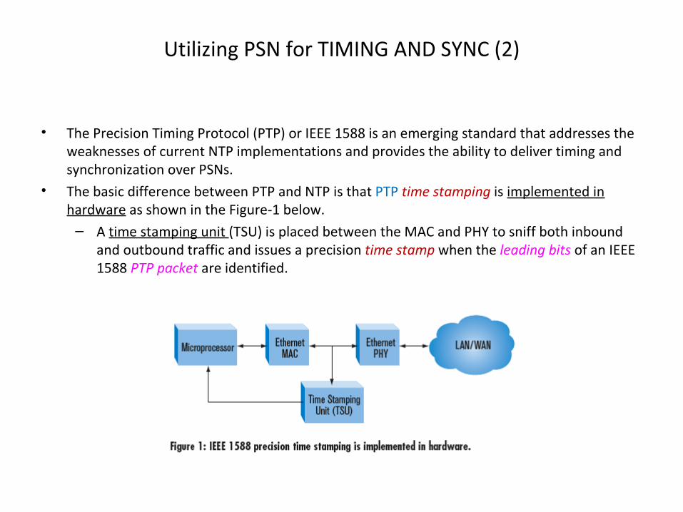
• The Precision Timing Protocol (PTP) or IEEE 1588 is an emerging standard that addresses the weaknesses of current NTP implementations and provides the ability to deliver timing and synchronization over PSNs.
• The basic difference between PTP and NTP is that PTP time stamping is implemented in hardware as shown in the Figure-1 below.
– A time stamping unit (TSU) is placed between the MAC and PHY to sniff both inbound and outbound traffic and issues a precision time stamp when the leading bits of an IEEE 1588 PTP packet are identified.
How IEEE 1588 PTP WORKS
• PTP (IEEE 1588) utilizes clocks configured in a tree hierarchy.– Master clocks can be installed in an existing building integrated timing supply (BITS)
located in master switching centers, and simple slave devices can be installed in remote base stations.
• The master clocks send messages to their slaves to initiate synchronization.– Each slave then responds to synchronize itself with the master.
• Incoming and outgoing PTP packets are time stamped at the start of frame (SOF) of the corresponding Ethernet packet.
– The protocol then exchanges information between the master and slave using IEEE 1588 message protocol.
– These messages are used to calculate the offset and network delay between time stamps, apply filtering and smoothing, and adjust the slave clock phase and frequency.
– This sequence is repeated throughout the network to pass accurate time and frequency synchronization.
• IEEE 1588 networks automatically configure and segment themselves using the best master clock (BMC) algorithm.
– The BMC enables hotswapping of nodes and automatically reconfigures the network in response to outages or network rearrangements.
How IEEE 1588 PTP WORKS (2)
• In order to estimate and mitigate operating system latency, the master clock periodically sends a sync message based on its local clock to a slave clock on the network.
• The TSU marks the exact time the sync message is sent, and a follow up message containing the exact time information is immediately sent to the slave clock.
• The slave clock time stamps the arrival of the sync message, compares the arrival time to the departure time provided in the follow up message, and then is able to identify the amount of latency in the operating system and adjust its clock accordingly.
• Network related latency is compensated for by measuring the roundtrip delay between the master and slave clocks.
• The slave periodically sends a delay request message to the master clock and the master clock issues a delay response message.
• Since both messages are precisely time-stamped, the slave clock can combine this information with the detail from the sync and follow up messages to gauge and adjust for network induced latency.

Another definitions
Pseudo Wire Timing Recovery
• Not all native services require timing recovery.• In general, non real-time services (such as data) do not need timing recovery at the
destination.• However, real-time services such as TDM do require timing recovery.• There are three basic approaches to timing recovery:
– Absolute,– Differential (DCR),– And adaptive (ACR).
• Regardless of the approach, you can generate the clock using analog or digital techniques.
Absolute Mode
• This is the normal method used for real-time protocol (RTP).• The sending end generates a time stamp that corresponds to the sampling time of the first
word in the packet payload.• The receiving end uses this information to sequence the messages correctly but without
knowledge of the sending end’s clock frequency.• This method is used when absolute frequency accuracy is not required.
Differential Mode (DCR)
• In the differential mode, both sending and receiving ends have access to the same high-quality reference clock.
• The sending end generates time stamps relative to the reference clock.• The receiving end uses the time stamps to generate a service clock that matches the
frequency relationship of the sending end’s service clock to the reference clock.• This method produces the highest quality clock and is affected least by network quality of
service (QoS) issues.
Adaptive Mode (ACR)
• The adaptive clock recovery (ACR) mode relies on packet inter-arrival time to generate the service clock frequency.
• This method does not (?) require time stamps or a reference clock to be present at the receiving end.
• However, it is affected by packet inter-arrival jitter.

HOW TO IMPLEMENTPart 2

The first implementation
Clock recovery for TDM PW over ATM-based PSN
• Synchronous – ATM IWF must be synchronized to the PRC clock• Asynchronous:
– Synchronous Residual Time Stamp (STRS) – the sender clock is recovered in the receiver with the use of SRTS timestamp.
• This method is known as Differential Clock Recovery (DCR)– Adaptive Clock Recovery (ACR) – Adaptive clock recovery based on the receiver buffer
occupancy.
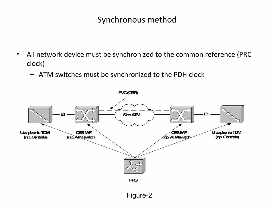
Synchronous method
• All network device must be synchronized to the common reference (PRC clock)– ATM switches must be synchronized to the PDH clock
Urządzenie TDM(np. Centrala)
Urządzenie TDM(np. Centrala)
CES IWF(np. ATM switch
CES IWF(np. ATM switch
E1 E1Siec ATM
PVC (CBR)
PRS
Figure-2
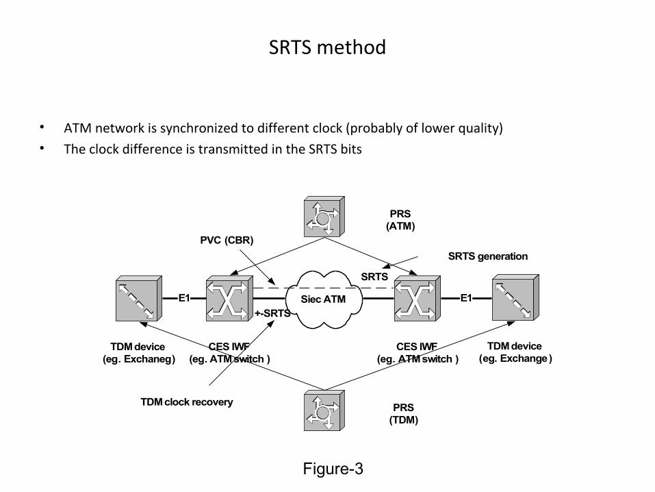
SRTS method
• ATM network is synchronized to different clock (probably of lower quality)• The clock difference is transmitted in the SRTS bits
TDM device(eg. Exchaneg)
TDM device(eg. Exchange)
CES IWF(eg. ATM switch )
CES IWF(eg. ATM switch )
E1 E1Siec ATM
PVC (CBR)
PRS (TDM)
PRS (ATM)
SRTS
+-SRTS
SRTS generation
TDM clock recovery
Figure-3
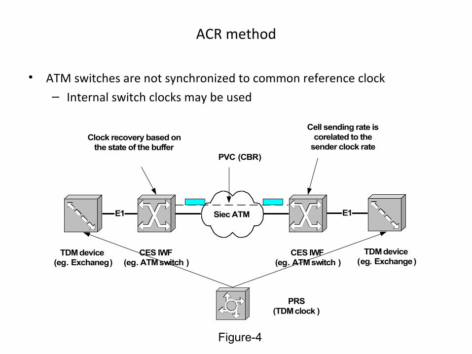
ACR method
• ATM switches are not synchronized to common reference clock– Internal switch clocks may be used
TDM device(eg. Exchaneg)
TDM device(eg. Exchange)
CES IWF(eg. ATM switch )
CES IWF(eg. ATM switch )
E1 E1Siec ATM
PVC (CBR)
PRS (TDM clock )
Cell sending rate is corelated to the
sender clock rateClock recovery based on
the state of the buffer
Figure-4
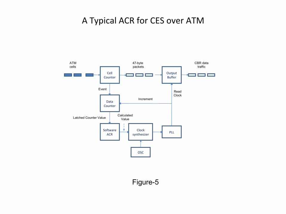
A Typical ACR for CES over ATM
ATM cells
Cell Counter
47-byte packets
Output Buffer
CBR data traffic
Data Counter
SoftwareACR
Clock synthesizer
OSC
PLL
Read Clock
Increment
Event
Latched Counter ValueCalculated
Value
Figure-5
A Typical ACR for CES over ATM (2)
• The received cells of the selected CBR data connection are counted by the Cell Counter.• After a configurable number of cells this counter will trigger an event.• At the same time, the Data Counter is incremented by the Read Clock of the Output Buffer.• The Data Counter will be latched by the event generated by the Cell Counter and the Counter
Value is passed to the Software ACR.• From this value and from information about the Output Buffer level the Software ACR
calculates the new value for the digital Clock Syntheziser.• The resulting clock is feet to a PLL, building the Read Clock for the 32kB Output Buffer.
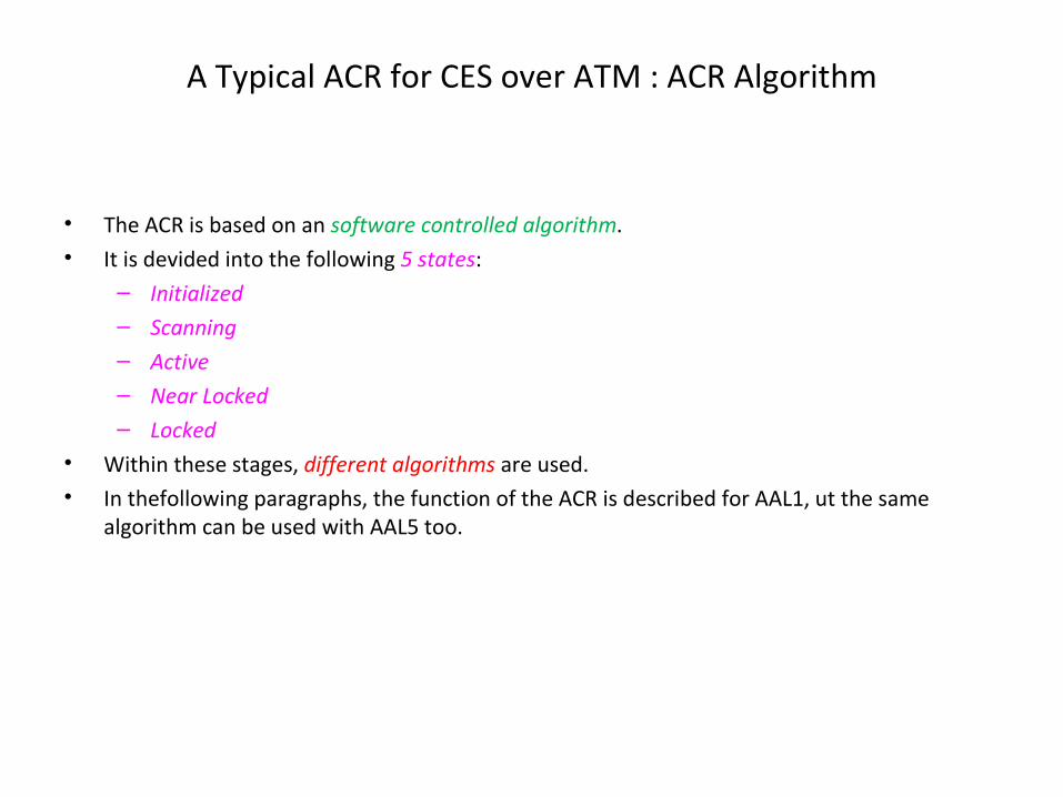
A Typical ACR for CES over ATM : ACR Algorithm
• The ACR is based on an software controlled algorithm.• It is devided into the following 5 states:
– Initialized – Scanning – Active – Near Locked – Locked
• Within these stages, different algorithms are used.• In thefollowing paragraphs, the function of the ACR is described for AAL1, ut the same
algorithm can be used with AAL5 too.
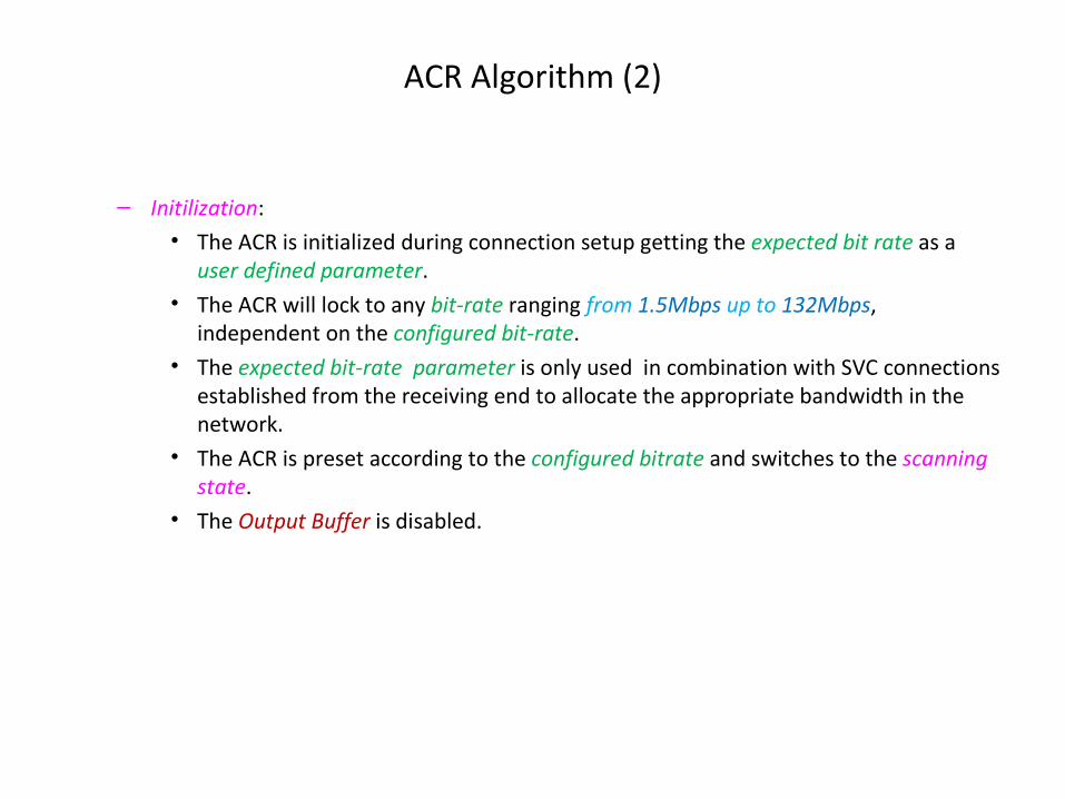
ACR Algorithm (2)
– Initilization:• The ACR is initialized during connection setup getting the expected bit rate as a
user defined parameter.• The ACR will lock to any bit-rate ranging from 1.5Mbps up to 132Mbps,
independent on the configured bit-rate.• The expected bit-rate parameter is only used in combination with SVC connections
established from the receiving end to allocate the appropriate bandwidth in the network.
• The ACR is preset according to the configured bitrate and switches to the scanning state.
• The Output Buffer is disabled.
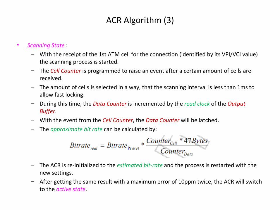
ACR Algorithm (3)
• Scanning State :– With the receipt of the 1st ATM cell for the connection (identified by its VPI/VCI value)
the scanning process is started.– The Cell Counter is programmed to raise an event after a certain amount of cells are
received.– The amount of cells is selected in a way, that the scanning interval is less than 1ms to
allow fast locking.– During this time, the Data Counter is incremented by the read clock of the Output
Buffer.– With the event from the Cell Counter, the Data Counter will be latched.– The approximate bit rate can be calculated by:
– The ACR is re-initialized to the estimated bit-rate and the process is restarted with the new settings.
– After getting the same result with a maximum error of 10ppm twice, the ACR will switch to the active state.
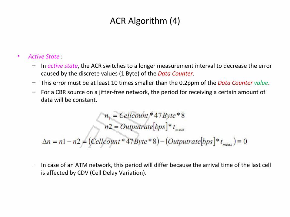
ACR Algorithm (4)
• Active State :– In active state, the ACR switches to a longer measurement interval to decrease the error
caused by the discrete values (1 Byte) of the Data Counter.– This error must be at least 10 times smaller than the 0.2ppm of the Data Counter value.– For a CBR source on a jitter-free network, the period for receiving a certain amount of
data will be constant.
– In case of an ATM network, this period will differ because the arrival time of the last cell is affected by CDV (Cell Delay Variation).
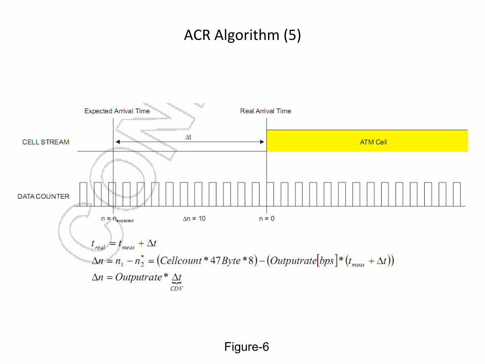
ACR Algorithm (5)
Figure-6
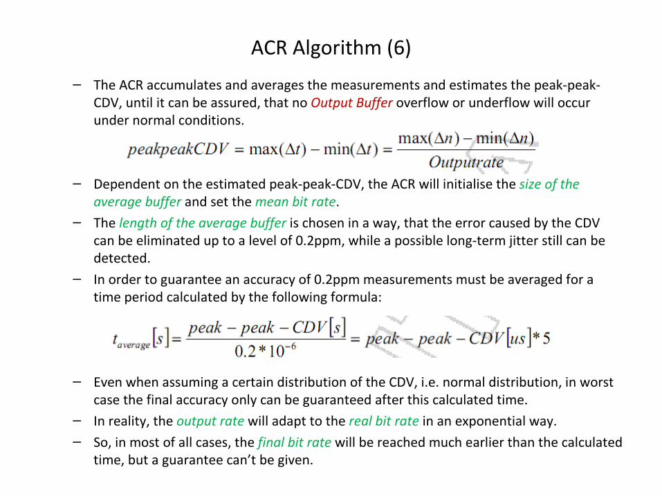
ACR Algorithm (6)
– The ACR accumulates and averages the measurements and estimates the peak-peak-CDV, until it can be assured, that no Output Buffer overflow or underflow will occur under normal conditions.
– Dependent on the estimated peak-peak-CDV, the ACR will initialise the size of the average buffer and set the mean bit rate.
– The length of the average buffer is chosen in a way, that the error caused by the CDV can be eliminated up to a level of 0.2ppm, while a possible long-term jitter still can be detected.
– In order to guarantee an accuracy of 0.2ppm measurements must be averaged for a time period calculated by the following formula:
– Even when assuming a certain distribution of the CDV, i.e. normal distribution, in worst case the final accuracy only can be guaranteed after this calculated time.
– In reality, the output rate will adapt to the real bit rate in an exponential way.– So, in most of all cases, the final bit rate will be reached much earlier than the calculated
time, but a guarantee can’t be given.
ACR Algorithm (7)• Near-locked State :
– In near-locked state, the ACR enables the Output Buffer, so that an output signal will be provided after the Output Buffer (FIFO) has reached its middle level of 16kB data.
– The Output Buffer is filled by the content of the received ATM cells (47 Bytes/Cell) and read out by the read clock genertated by the ACR.
– Additional to the measurement described above, the ACR uses the Output Buffer level and the slope of the Output Buffer level for calculating the new output rate.
– The Output Buffer level is the difference between the received data and the output data aggregated over the time.
– If the level of the Output Buffer stays within a certain range, which depends on the estimated CDV, no action is taken by the ACR.
– By this approach the short term jitter caused by the CDV will be ignored.– If the average level of the Output Buffer has a certain slope (constantly increasing or decreasing) a
change of the input rate at the sending side (long term jitter) must be assumed.– In this case, the ACR will follow this change, otherwise a buffer overflow or underflow will occur after
a longer time. – While in this stage, the neither accuracy nor the wander of the output bit rate can be guaranteed to
fulfil the specifications.– The ACR fills the average buffer with new measurements.– After collecting and averaging measurements for the calculated interval length the ACR will switch to
the locked state.
ACR Algorithm (8)
• Locked State :– In locked state, the ACR uses the same measurements than in the near-locked state, but
overwrites with each new measurement the oldest value in the average buffer.– In order to fulfil the requirements of the PAL, SDI and PCR jitter requirements, the
change of the output rate will be limited to 0.02ppm/s.– The resulting output rate will show only very slow and tiny changes.– The ACR will stay in the locked state, until either the connection is released or an error,
i.e. an interruption of the connection in the network occurs.

The second implementation
Clock Generation
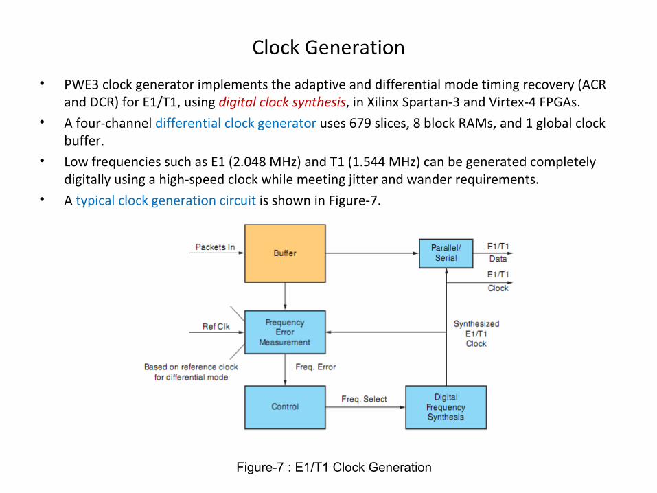
• PWE3 clock generator implements the adaptive and differential mode timing recovery (ACR and DCR) for E1/T1, using digital clock synthesis, in Xilinx Spartan-3 and Virtex-4 FPGAs.
• A four-channel differential clock generator uses 679 slices, 8 block RAMs, and 1 global clock buffer.
• Low frequencies such as E1 (2.048 MHz) and T1 (1.544 MHz) can be generated completely digitally using a high-speed clock while meeting jitter and wander requirements.
• A typical clock generation circuit is shown in Figure-7.
Figure-7 : E1/T1 Clock Generation
Clock Generation (2)
• Note that the circuit behaves like a phase lock loop (PLL), where the frequency error is based on the buffer fill level for the adaptive mode (ACR) and on the reference clock for the differential mode (DCR).
• Based on FPGA, it can help to implement adaptive- and differential-mode timing recovery (ACR and DCR) for E1/T1 using digital clock synthesis.
• The advantages of our solution are the linearity of the digitally controlled oscillator (DCO) and the ability to configure the frequency resolution to very small values.

Using Jitter Buffers(The method used to mitigate the effects of delay variation is the use of a jitter buffer)
Background
• Ideally, since frames are transmitted at regular intervals, they should reach the destination after some fixed delay.
• If the transmission delay through the network were indeed constant, the frames would be received at regular intervals and in their original transmission order.
• In practice, the transmission delay varies because of several factors: – Intrinsic jitter at the transmit side, described above – Variations in the transmission time through the network, caused by the frame handling
method:• frames pass through many switches and routers, and in each of them the frame (or
the packet encapsulated in the frame) is first stored in a queue with frames or packets from other sources, and is then forwarded to the next link when its time arrives.
– Intrinsic jitter at the receive side, due to the variation in the time needed to extract the payload from the received packets.
Jitter Buffer Functions
• Any network designed for reliable data transmission must have a negligibly low rate of data loss.
• Therefore, it is reasonable to assume that essentially all the transmitted frames reach their destination.
• Under these circumstances, the rate at which frames are received from the network is equal to the rate at which frames are transmitted by their source (provided that the measurement is made over a sufficiently long time).
• As a result, it is possible to compensate for transmission delay variations by using a large enough temporary storage.
• This storage, called jitter buffer, serves as a first-in, first-out (FIFO) buffer.
Jitter Buffer Functions (2)
• The buffer has two clock signals: – Write clock, used to load packets into the buffer.
• Since each packet is loaded immediately after being successfully received from the network, packets are written into the buffer at irregular intervals.
– Read clock, used to transfer packets to the packet processor at a fixed rate.• The jitter buffer operates as follows:
– At the beginning of a session, the buffer is loaded with a conditioning pattern until it is half full.
• No bits are read from the buffer at this time.• Therefore, a delay is introduced in the data path.
– After the buffer reaches the half-full mark, the read-out process is started.• The data bits are read out at an essentially constant rate.• To prevent the buffer from either overflowing or becoming empty (underflow), the
read-out rate must be equal to the average rate at which frames are received from the network.
• Therefore, the buffer occupancy remains near the half-full mark.• The buffer stores the frames in accordance with their arrival order.
Selecting an Optimal Jitter Buffer Size
• For reliable operation, the jitter buffer must be large enough to ensure that it is not emptied when the transmission delay increases temporarily (an effect called underflow, or underrun), nor fills up to the point that it can no longer accept new frames when the transmission delay decreases temporarily (an effect called overflow).
• The minimum size of a jitter buffer depends on the intrinsic jitter: usually, the minimum value is 3 msec.
• The maximum size is 300 msec. • The theoretically correct value for the size of the jitter buffer of any given bundle is slightly
more than the maximum variation in the transmission delay through the network, as observed on the particular link between the bundle source and the destination.
• For practical reasons, it is sufficient to select a value that is not exceeded for any desired percentage of time:
– for example, a value of 99.93% means that the jitter buffer will overflow or underflow for an accumulated total of only one minute per day.
Selecting an Optimal Jitter Buffer Size (2)
• Jitter buffers are located at both ends of a link, therefore the delay added by the buffers is twice the selected value.
• The resultant increase in the round-trip delay of a connection may cause problems ranging from inconvenience because of long echo delays on audio circuits (similar to those encountered on satellite links) to time-out of data transmission protocols.
• Therefore, the size of each jitter buffer must be minimized, to reduce the round-trip delay of each connection in as far as possible, while still maintaining the link availability at a level consistent with the application requirements.
Adaptive Timing
• Because of the transmission characteristics of packet switching networks (PSN), which use statistical multiplexing, the average rate must be measured over a sufficiently long interval.
• The optimal measurement interval is equal to the difference between the maximum and minimum transmission delays expected in the network.
• As explained above, the buffer is used to store packets for an interval equal to the maximum expected delay variation.
• Therefore, this buffer can be used by the adaptive timing (ACR) mechanism, to recover a clock having a frequency equal to the average transmit rate.
Adaptive Timing (2)
• The method used to recover the payload clock of a bundle is based on monitoring the fill level of the jitter buffer:
– the clock recovery mechanism monitors the buffer fill level, and generates a read-out clock signal with adjustable frequency.
• The frequency of this clock signal is adjusted so as to read frames out of the buffer at a rate that keeps the jitter buffer as near as possible to the half-full mark.
• This condition can be maintained only when the rate at which frames are loaded into the buffer is equal to the rate at which frames are removed.
Adaptive Timing (3)
• Assuming that the IP network does not lose data, the average rate at which payload arrives will be equal to the rate at which payload is transmitted by the source.
• Therefore, the adaptive clock recovery (ACR) mechanism actually recovers the original payload transmit clock.
• This mechanism described above also generates a clock signal having the frequency necessary to read-out frames at the rate that keeps the jitter buffer as near as possible to the half-full mark.
• The bundle used as the basis for recovering the adaptive clock can be selected by the user.

COMPARISON B/W COMPETITORSPart 3
Some popular Stds/Recs
• In the past, the TDMoIP preferably uses the network central clock. However, it can also use adaptive or RTP-based techniques.
– The RTP provides a Layer-4 timestamp.– If TDMoIP provides AAL1 payload, it uses Layer-2 timestamps with SRTS (assuming a
common clock, but not necessarily the physical layer one). • The CESoPSN uses RTP-based synchronization by default. Anyway, optionally, an adaptive
synchronization or network central clock could be used as well.• The IETF CEoP for Sonet/SDH (RFC4842) uses Stratum-3 network central clock at least.• And now, a Layer-2 timestamp is being suggested in Ethernet frames (IEEE with Std 1588-
2002 version 2, then 802.1AS now).– After, ITU-T with G.8261 based on Ethernet physical layer as well as Layer-2.
Some popular implementations
• Device:– The AimCom and Zarlink devices both support G.8261 (synchronous Ethernet).– Maxim, Zarlink and Transwitch devices supports RTP.
• System:– Resolute Networks systems support IEEE 1588 (independently to physical layer, with
both frequency and time transmission).– For the Axerra systems (on website) uses IETF RTP.– The RAD's uses ITU-T G.8261.