Embed Size (px)
Citation preview
Time-resolved Characterization of
Non-equilibrium Carrier Dynamics in
Gallium Based III-V Materials and Devices
By
Jie Zhang
Submitted in Partial Fulfillment
of the
Requirements for the Degree
Doctor of Philosophy
Supervised by
Professor Roman Sobolewski
Department of Electrical and Computer Engineering
Arts, Sciences and Engineering
Edmund A. Hajim School of Engineering and Applied Sciences
University of Rochester
Rochester, New York
2012

ii
Dedicated to my wife and family…
iii
Curriculum Vitae
Jie Zhang was born in Jiangyan, Jiangsu, China, in 1982. He attended Nanjing University,
China, from 1999 to 2006, graduating with a Bachelor of Science degree in 2003 and a
Master of Science degree in radio physics in 2006. In the fall of 2006, he enrolled in the
PhD program in the Department of Electrical and Computer Engineering at the
University of Rochester. He pursued his research in the Ultrafast Quantum Phenomenon
Laboratory under the direction of Professor Roman Sobolewski and received the Master
of Science degree in 2009. He received the Frank J. Horton Fellowship at the University
of Rochester from 2007 to 2012.
iv
List of Presentations
◇ J. Zhang, M. Mikulics, R. Adam, D. Grützmacher and R. Sobolewski, “Generation of THz
transients by photo-excited single crystal GaAs meso-structures”, ICPEPA_8, Rochester,
August 2012 (Oral presentation).
◇ J. Zhang, M. Mikulics, J. Serafini, M. Gong, R. Adam, D. Grützmacher and R. Sobolewski,
“An ultrafast GaAs Nano-Whisker photodetector for THz range application”, CLEO,
Baltimore, May 2011 (Poster presentation).
◇ J. Zhang, A. Belousov, S. Katrych, J. Jun, K. Hametner, D. Günther, J. Karpinski, B. Batlogg
and R. Sobolewski, “Femtosecond pump-probe characterization of high-pressure grown
AlxGa1-xN single crystals”, Proc. of SPIE, San Jose, Jan. 2009 (Oral presentation).
◇ J. Zhang, A. Belousov, J. Karpinski and R. Sobolewski, “Propagation of multiple
coherent-acoustic-phonon transients in GaN single crystals”, 1st International Symposium on
Laser Ultrasonics, Montreal, Canada, July 2008 (Oral presentation).
v
List of Publications
◇ J. Zhang, M. Mikulics, R. Adam, D. Grützmacher and R. Sobolewski, “Generation of THz
transients by photo-excited single crystal GaAs meso-structures”, submitted to Appl. Phys. B.
◇ J. Zhang, A. Belousov, J. Karpinski and R. Sobolewski, “Direct measurement of
coherent-acoustic-phonon lifetime in GaN single crystals”, submitted to Appl. Phys. Lett.
◇ M. Mikulics, J. Zhang, J. Serafini, R. Adam, D. Grützmacher and R. Sobolewski,
“Sub-picosecond electron-hole recombination time and terahertz-bandwidth photoresponse
in freestanding GaAs epitaxial meso-structures”, Appl. Phys. Lett., 101, 031111, (2012).
◇ J. Zhang, A. Belousov, J. Karpinski, B. Batlogg, Gary Wicks, and Roman Sobolewski,
“Time-resolved femtosecond optical characterization of multi-photon absorption in
high-pressure-grown Al0.86Ga0.14N single crystals”, J. Appl. Phys. 110, 113112 (2011).
◇ M. Mikulics, P. Kordoš, D. Gregušová, R. Adam, M. Kočan, S. Wu, J. Zhang, R. Sobolewski, D.
Grützmacher, and M. Marso1, “Monolithic Integration of Ultrafast Photodetector and
MESFET in the GaN Material System”, IEEE Photonic Technology Letters, 23, 17, 1189-1191,
(2011).
◇ J. Zhang, M. Mikulics, J. Serafini, M. Gong, R. Adam, D. Grützmacher and R. Sobolewski,
“An ultrafast GaAs Nano-Whisker photodetector for THz range application”, in CLEO:2011 -
Laser Applications to Photonic Applications, OSA Technical Digest (Optical Society of America,
2011), paper JTuI19.
◇ B. Ciftcioglu, J. Zhang, R. Sobolewski and H. Wu, “A 850 nm Germanium
Metal-Semiconductor-Metal Photodetector with 13-GHz Bandwidth and 8 A Dark Current”,
IEEE Photonic Technology Letters, 20, 24, 2069-2071, (2010).
◇ J. Zhang, A. Belousov, S. Katrych, J. Jun, K. Hametner, D. Günther, J. Karpinski, B. Batlogg
and Roman Sobolewski, “Femtosecond pump-probe characterization of high-pressure grown
AlxGa1-xN single crystals”, Proc. of SPIE, Vol. 7216 721623-1, (2009).
◇ B. Ciftcioglu, L. Zhang, J. Zhang, J.R. Marciante, J.D. Zuegel, R. Sobolewski, and H. Wu,
vi
"Integrated Silicon PIN Photodiodes Using Deep Nwell in a Standard 0.18-um CMOS
Technology," IEEE Journal of Lightwave Technology, 27(15), 3303-3313, (2009).
◇ A. Belousov, S. Katrych, J. Jun, J. Zhang, D. Günther, Roman Sobolewski, J. Karpinski, and B.
Batlogg, “Bulk single-crystal growth of ternary AlxGa1−xN from solution in gallium under high
pressure”, Journal of Crystal Growth, 311, 16, 3971-3974, (2009).
◇ B. Ciftcioglu, J. Zhang, L. Zhang, J.R. Marciante, J.D. Zuegel, R. Sobolewski, and H. Wu,
"3-GHz Silicon Photodiodes Integrated in a 0.18-um CMOS Technology", IEEE Photonic
Technology Letters, 20, 24, pp. 2069-2071, (2008).
◇ S. Wu, J. Zhang, A. Belousov, J. Karpinski, and R. Sobolewski in Gallium Nitride Materials
and Devices III, "Dynamics of intervalley transitions and propagation of coherent acoustic
phonons in GaN single crystals studied by femtosecond pump-probe spectroscopy," ed. by H.
Morkoc, C. W. Litton, J.-I. Chyi, Y. Nanishi, and E. Yoon, Proc. of SPIE, 6894, 68940K, (2008).
◇ S. Wu, J. Zhang, A. Belousov, J. Karpinski, R. Sobolewski, “Ultra-Long-lived coherent
acoustic phonons oscillations in GaN single crystals”, Journal of Physics: Conference Series 92
(2007).
◇ J. Zhang, J. Chen, J. Wu, L. Kang, W. Xu and P. H. Wu, “Acid eroding process for the
fabrication of Bi2Sr2CaCu2O8+x junctions”, Chinese Science bulletin, 52, 303 (2007).
vii
Acknowledgement
First and foremost, I would like to express my gratitude to my advisor, Professor Roman
Sobolewski, who provided guidance, support and encouragement from the beginning to
the end to help me develop an understanding of the subject and make this thesis possible.
He has set a good example for me by his optimistic attitudes and persistence in pursuit of
science. I feel very honored and privileged to have worked with him.
I would like to extend my sincere gratitude to Prof. William Donoldson, Prof. Gary
Wicks, Prof. Qiang Lin, and Prof. Hui Wu. Without their help and guidance on the project,
this thesis would not have been possible. I would also like to thank Prof. Thomas Hsiang,
Prof. Hanan Dery, Prof. Philips Fauchet, and Dr. Svetlana Lukishova for their valuable
help on my classes, lab works and oral exams.
I would also like to thank our collaborators: Prof. Janusz Karpinski, Dr. Martin Mikulics,
Prof. Javier Mateos and Prof. A. M. Song, for their supply of high quality samples.
I am deeply indebted to all of my former and present groupmates in Prof. Sobolewski's
Ultrafast Quantum Phenomena group, Dr. Shuai Wu, Dr. Daozhi Wang, Dr. Xia Li Cross,
Dr. Dong Pan, Dr. Allen Cross, Dr. Mufei Gong, Cheng Zhao, John Stefani, Pingyue
viii
Song and Yuhan Wang. Without their help, discussions and friendships, my research work
would have been much more difficult than it was. I would also like to thank Yunliang Zhu
in Prof. Wu's group, Yijin Fu in Prof. Fauchet's group, Zongmin Bei in Prof. Jones' group,
for their help and cooperation on various research projects.
I would like to thank all my friends I met in Rochester, Xian Zhang, Jun Zhou, Zhiyong
Mao, Zhuoxun Chen, Jun Cai and Zhaoke Jia. Their friendships have been valuable to me
during my study in Rochester.
This work was partially supported by NSF grant No. ECCS-0901701 (Rochester), U.S.
Department of Energy Office of Inertial Confinement Fusion under Cooperative
Agreement No. DE-FC52-08NA28302 and the New York State Energy Research and
Development Authority. I would like to thank the National Science Foundation and the
Laboratory of Laser Energetics for their support. The support of DOE does not constitute
an endorsement by DOE of the views expressed in this article.
Finally, I would like to thank my wife, my parents, and my parents-in-law for their
unconditional love, support and encouragement in my life. No matter where I was, they
were always with me, so this thesis is dedicated to my family.
ix
Abstract
Ga-based III-V materials, such as, GaAs, GaN and AlGaN, have a wide-range of
applications in the fields of high-speed, high-temperature, high-power and
high-frequency electronic and optoelectronic devices, due to their unique physical
properties. This thesis is devoted to the time-resolved characterization of ultrafast,
nonequilibrium carrier and phonon dynamics in Ga-based III-V materials and their
devices. I present my studies of coherent acoustic phonons (CAPs) and nonlinear optical
(NLO) process in GaN and AlGaN single crystals, as well as the ultrafast characterization
of epitaxially-grown GaAs meso-structured photodetectors (PDs) and self-switching
diodes (SSDs) operating as novel THz emitters and photon sensors.
Studies of CAPs and NLO properties in III-Nitrides were accomplished using a
femtosecond time-resolved pump-probe spectroscopy. We have experimentally
investigated the generation, propagation and detection mechanisms of CAPs and, with the
two-side CAPs detection scheme, the intrinsic phonon lifetime was measured to be 80 ns
in GaN single crystals at room temperature. The NLO properties of AlGaN single crystals
were studied by means of a multi-photon absorption (MPA) technique. My research
shows that AlGaN exhibits a large nonlinear correlation factor, with a strong, 310-fs-wide
correlation peak. Furthermore, our analysis of the correlation peak amplitude on the
pump wavelength allowed us to demonstrate that its spectral dependence agreed very
well with the Sheik-Bahae and Hutchings theory for the two-photon absorption (TPA)
x
process. The latter indicates that the TPA process in AlGaN sample in our experiment
consisting of one pump and one second-harmonic generation (SHG) of probe photons.
I further report optical characterization of a novel PD device based on
epitaxially-grown, single crystal GaAs. Our freestanding PD features an extremely low
dark current of only 2×10⁻⁹ A and responsivity of 4.4 mA/W at 30 V. Its photon detection
efficiency is ~ 7%. The time-domain electro-optical sampling (EOS) measurement results
show that the PD has an ultrafast ~ 310 fs photoresponse, corresponding to a bandwidth
of 1.4 THz. With a double-pulse optical excitation, the PD was tested for successful
operation under ~ 1 THz clock rate. All the above properties make it a device-of-choice
for future high-speed, high repetition rate, low power consumption optoelectronic
application.
GaAs-based SSDs have already shown their unique performance in microwave
harvest and are predicted to be high-efficient THz emitters. We present here, for the first
time, the time-resolved transient THz radiation signal generated by a photo-excited and
biased SSD. The signal exhibits ~730 fs full-width-at-half-maximum (FWHM),
corresponding to a 0.5 THz bandwidth burst.
xi
Table of Contents
List of Figures ...........................................................................................................................................xiii
Nomenclature .......................................................................................................................................... xvii
Foreword ................................................................................................................................................... xix
1. Ga-based III-V materials introduction ......................................................... 1
1.1 Ga-based III-V materials overview ........................................................................................... 2
1.1.1 Properties of the Ga-based III-V semiconductors ........................................................... 3
1.1.2 Applications for Ga-based III-V semiconductors ............................................................ 6
1.2 Carrier and phonon dynamics in semiconductors ................................................................. 6
1.3 Thesis outline ............................................................................................................................... 9
Bibliography ............................................................................................................................................12
2. Experimental techniques ...................................................................... 14
2.1. Mode-locked femtosecond laser system .................................................................................14
2.2. Impulse response measurement ..............................................................................................17
2.3. Time-resolved femtosecond pump-probe spectroscopy ......................................................19
2.4. Transient THz electro-optic sampling .....................................................................................23
2.4.1 In-plane electro-optic sampling ....................................................................................... 23
2.4.2 Free-space THz spectroscopy ........................................................................................... 26
Bibliograghy ............................................................................................................................................29
3. Ultrafast carrier and phonon dynamics in III-Nitride semiconductors ................... 31
3.1. III-Nitride single crystals growth ............................................................................................32
3.1.1 GaN single crystal growth ................................................................................................ 32
3.1.2 (Al,Ga)N single crystal growth ........................................................................................ 34
3.2. Optical properties of III-Nitrides .............................................................................................36
3.3. Nonlinear optical property study of bulk III-Nitrides ..........................................................39
xii
3.3.1 Degenerate and non-degenerate two-photon absorption ............................................ 40
3.3.2 TPA coefficient measurement .......................................................................................... 42
3.3.3 Two-photon non-degenerative absorption measurement of GaN single crystals .... 43
3.3.4 Multi-photon absorption measurement of bulk (Al,Ga)N single crystals ................. 46
3.4. Coherent acoustic phonon dynamics in GaN single crystals...............................................57
3.4.1 Generation of CAPS in GaN single crystals ................................................................... 58
3.4.2 Detection of CAPs.............................................................................................................. 59
3.4.3 Propagation of CAPs in GaN ........................................................................................... 60
3.4.4 CAP lifetime measurement .............................................................................................. 63
3.5. OEICs-based GaN devices ........................................................................................................67
3.6. Summary .....................................................................................................................................70
Bibliography ............................................................................................................................................72
4. THz bandwidth photo-response of free-standing GaAs meso-structures ................. 75
4.1. Free-standing GaAs epitaxial meso-structures fabrication ..................................................76
4.2. DC characteristics of GaAs whisker ........................................................................................77
4.3. Time-resolved photoresponse of epitaxial grown GaAs single crystal meso-structures .80
4.4. Summary .....................................................................................................................................90
Bibliography ............................................................................................................................................92
5. THz radiation measurement from self-switching diodes .................................. 94
5.1. Introduction to self-switching device ......................................................................................95
5.2. Applications of self-switching devices....................................................................................97
5.3. DC characteristics and impulse responses of SSDs ...............................................................99
5.4. THz radiation measurement of the SSDs ..............................................................................102
Bibliography ..........................................................................................................................................105
6. Conclusions .................................................................................. 106
6.1. Thesis summary .......................................................................................................................106
6.2. Future work ..............................................................................................................................108
xiii
List of Figures
1.1 Band structure of gallium arsenide. ................................................................................................ 3
1.2 Representative dynamics processes in semiconductors, taking place within different
time scales.. .......................................................................................................................................... 7
2.1 The energy level diagram of Ti:sapphire, together with the absorption and emission
spectra. Interaction of the titanium electron with the Al2O3 lattice produces wide
spreading of the energy levels and results in broad tuning. .......................................................15
2.2 Self-focusing of Kerr lens effect, the outer region of the CW beam is then blocked away
by a slit, resulting a self-amplifying pulsed beam. .......................................................................17
2.3 (a) Impulse response test setup using a modelocked Ti:Al2O3 femtosecond laser and a
50-GHz sampling oscilloscope. (b) Impulse response results of a Ge MSM PD at 800 nm
illumination and 7 V bias..................................................................................................................18
2.4 Ultrafast optical pump and probe setup for carrier and phonon dynamics
characterization in GaN single crystals. .........................................................................................20
2.5 An EO modulator with a x-cut LiTaO3 crystal used in the transverse geometry. The
incident light polarization is 45° with respect to the z-axis. ........................................................24
2.6 A typical in-plane EOS setup using LiTaO3 platelet as the EO sensor. .....................................26
2.7 Schematic setup for free-space THz detection using ZnTe EO crystal. .....................................28
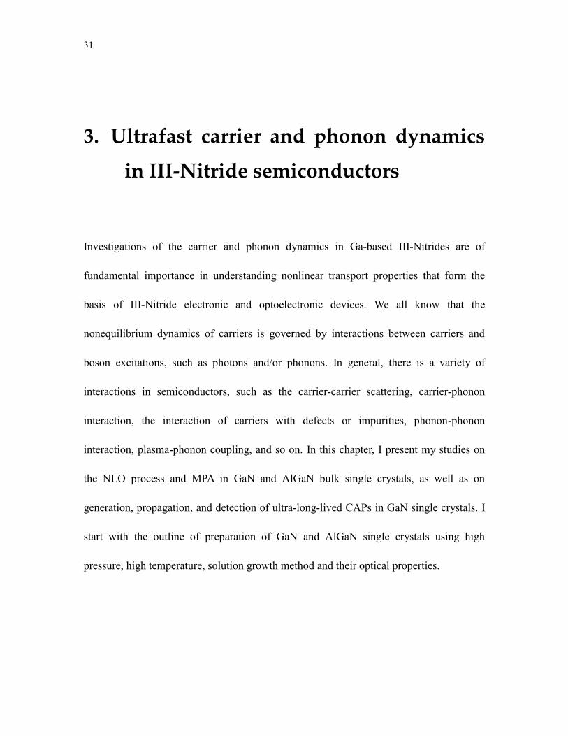
3.1 Pressure intensifier and high pressure – high temperature crystal growth chamber for
nitrogen pressure up to 15 kbar. 1) 3-mantle high pressure chamber with cooling
jacket, 2) press piston, 3) integral body of the intensifier, 4) piston, 5) screw, 6) plug
with electrical leads, 7) heater with crucible and sample, 8) cooling system, 9) capillary. ......33
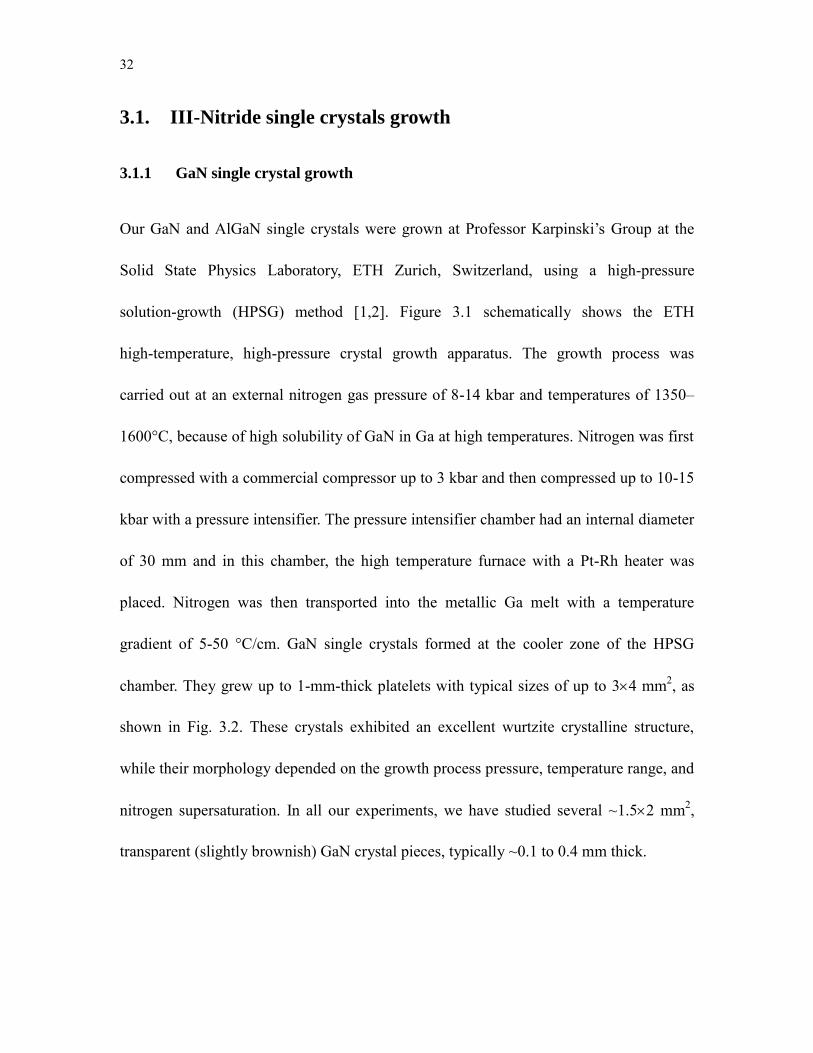
3.2 Representative GaN single crystal prepared by the HPSG method. .........................................33
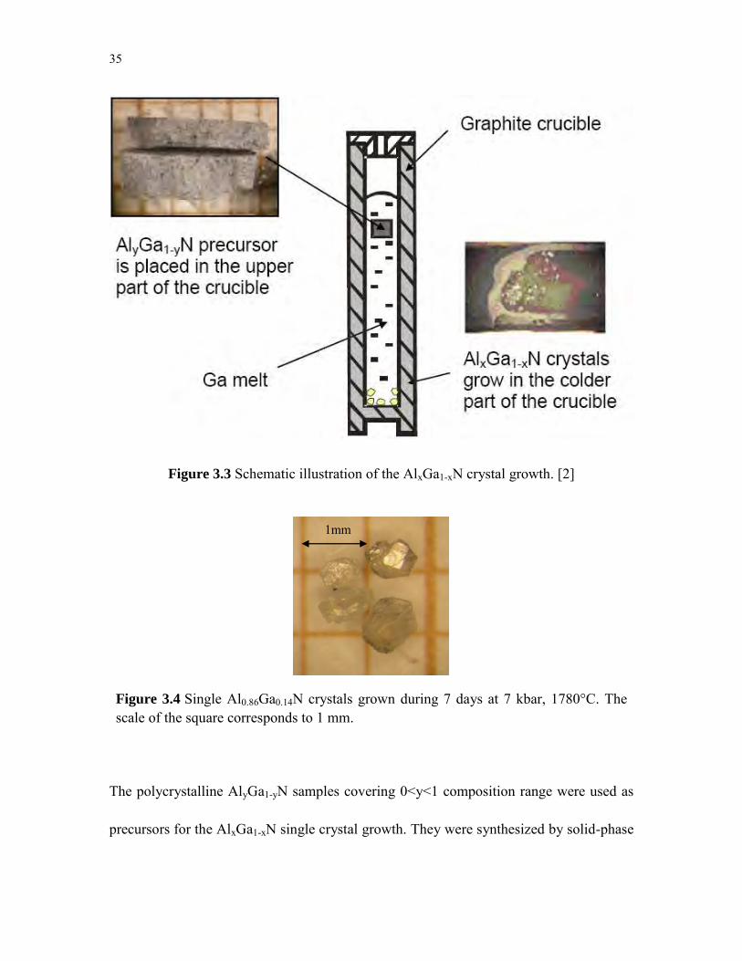
3.3 Schematic illustration of the AlxGa1-xN crystal growth. ...............................................................35
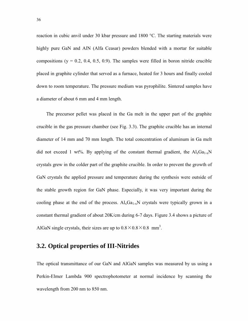
3.4 Single Al0.86Ga0.14N crystals grown during 7 days at 7 kbar, 1780°C. The scale of the
square corresponds to 1 mm. ...........................................................................................................35
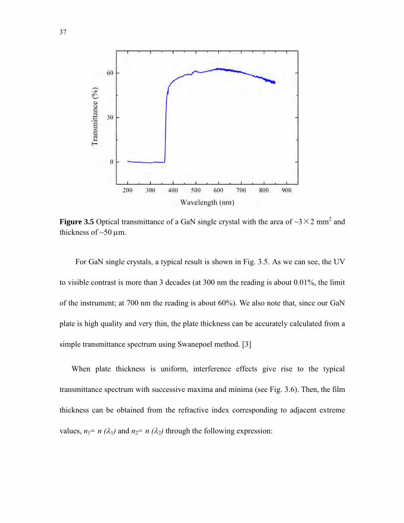
3.5 Optical transmittance of a GaN single crystal with the area of ~3×2 mm2 and thickness
of ~50 m. ............................................................................................................................................37
3.6 Enlarged area of Fig. 3.5 at wavelength ranging from 560 – 700 nm, showing the
interference fringes of the transmission spectrum. .......................................................................38
xiv 3.7 Optical transmittance of an irregular Al0.84Ga0.16N single crystal with the size of
~0.8×0.8×0.8 mm3. ...........................................................................................................................38
3.8 Schematic of a nonlinear optical MPA measurement setup. .......................................................43
3.9 Two-photon absorption induced transmission decrease in GaN single crystal,
cross-correlation between the idle beams and their second-harmonics, wavelengths
from 730 nm to 810 nm. ....................................................................................................................45
3.10 Pulse width of the TPA signal at different probe wavelengths. ...................................................45
3.11 (a) Time-resolved ∆T/T transient measured for the UV λ = 380 nm pump and IR λ = 760
nm probe beams. The red dotted line represents a theoretical fit. (b) The same ∆T/T
transient (black squares), but on a much-shorter time scale. The blue triangles are the
best fit corresponding to a Gaussian-shaped correlation signal of the pump and probe
photons. The green circles fit the photoresponse component of the transient, with the
rising part represented by the error function and the decay modeled as a
double-exponent relaxation. The red squares correspond to the superposition of the
correlation and photoresponse components and overlay the experimental data. The fit
of red squares in (b) is identical to the red dotted line in (a). ......................................................47
3.12 The dependence of the ∆T/T correlation signal amplitude on the energy of the photons
of the Ti-sapphire laser. The solid line is a guide to the eye. .......................................................50
3.13 ∆T/T correlation signal (solid squares) and relaxation signal (solid circles) amplitudes
versus the pump power intensity, measured at the 380-nm pump wavelength. The solid
line is the linear best fit and its slope is proportional to the γ(ωpu, ωpr, ωpr) or,
equivalently, β(ωpu, 2ωpr) coefficients in Eqs. (3-10) and (3-11), respectively. The dotted
line is the linear fit corresponding to the first term in Eq. (3-12). The error bars define
the experiment background noise in our pump-probe measurements. .....................................54
3.14 The nonlinear correlation factor (NCF–the slope of the ∆T/T correlation signal
amplitude vs. Ipu) as a function of the pump beam wavelength. The red circles are our
experimental data points, while the solid lines correspond the β(λpu) and γ(λpu)
functional dependences, representing Eq. (3-3) and Eq. (3-15), respectively. The NCF
value for λpu = 380 nm is indicated. .................................................................................................55
3.15 Simulation of spatial-time profiles of propagating CAP transients generated by the
electronic stress, thermal stress, and both, respectively. The CAP pulse was excited by
the pump beam with the photon energy of 4.59 eV. The inset shows the frequency
spectra of the electronically (solid line) and thermal induced (dashed line) CAPs. ................59
3.16 ΔR/R signal measured in one-colour configuration at the wavelength of 355 nm. (a) Full,
time-resolved ΔR/R transient. (b) CAP oscillations extracted from the ΔR/R signal. The
solid line is simple-damped sinusoidal fit, based on equation (3-17). The inset in (b) is a
fast Fourier transform (FFT) of the oscillatory data. .....................................................................61
3.17 Time-resolved R/R waveform as a function of the pump-probe delay time, measured
in a ~50 m thick GaN single crystal for pump/probe wavelengths of 355 nm/710 nm,
corresponding to just-above-band-gap excitation. The oscillations are due to the CAP
propagation in GaN single crystals. ................................................................................................62
xv 3.18 Schematic pump-probe spectroscopy setup for all optical generation and detection of
CAPs in GaN single crystals; both one and two-sided measurement geometries were
adopted in order to achieve the direct CAP lifetime measurement. ..........................................64
3.19 (a) Two-sided experimental geometry for direct measurement of the CAP lifetime. (b)
CAP oscillations obtained at the front surface of the GaN single crystal right after the
generation of acoustic phonons. (c) CAP oscillations obtained on the back surface of the
GaN sample, after CAP has propagated a distance of the sample’s thickness (~ 4 ns).
The solid red lines on the experimental data are the best fitting of the oscillations using
Eq. (3-17). The insets of the (b) and (c) show the Fourier transform of the two data sets
and have the same peak frequency of 52 GHz. .............................................................................66
3.20 Normalized CAP oscillation amplitude at various time positions: the circles represent
the experimental data; the squares are taken from data in ref. [20], which was
measured using one-side geometry; the solid line is an exponential fitting. The CAP
intrinsic lifetime in GaN single crystal was measured to be 80±3 ns. .........................................67
3.21 OEIC circuit containing an MSM PD integrated with MESFET in a CPS line layout
fabricated on GaN/AlN/SiC. The meander structure that biases the gate acts as an
inductor to block the high-frequency signal from the PD. ..........................................................69
3.22 OEIC circuit containing an MSM PD integrated with MESFET in a CPS line layout
fabricated on GaN/AlN/SiC. The meander structure that biases the gate acts as an
inductor to block the high-frequency signal from the PD. ..........................................................70
4.1 Schematics of the epitaxial GaAs nanowhikser fabrication process. .........................................79
4.2 Current-voltage characteristics of a GaAs freestanding whisker placed on an MgO
substrate and incorporated in a CPS transmission line (see bottom inset). The
characteristics were measured in the dark (green squares), and under 850-nm-
wavelength, 0.2-mW nominal power continuous illumination (dark blue dots),
respectively. The top inset presents the responsivity of our device. ..........................................80
4.3 (a) Transient photoresponses of a GaAs whisker photodetector illuminated with a
100-fs-wide, 800-nm-wavelength, and 1-mW incident power optical pulses. The
detector bias was 20 V. The black curves are experimental data recorded at 137-µm and
171-µm positions away from the device (see inset), respectively, while red curves are
numerical fits. The time interval between the two pulses is 294 fs and directly
corresponds to the 34 µm of the propagation distance along the CPS. (b) FWHM values
of experimental transients (solid triangles) recorded at several distances along the CPS
away from the detector plane. The solid dot represents the 320-fs FWHM value of the
intrinsic pulse generated by the whisker. The inset in (b) shows the spectral
characteristics of the calculated, intrinsic, zero-propagation distance transient. The 3-dB
and 10% spectral ranges are marked. .............................................................................................81
4.4 (a) The calculated attenuation constant (green curve) and the quadratic fitting (red
curve). (b) phase factor of the CPS line. .......................................................................................84
4.5 Pump-probe spectroscopy results of the GaAs platelet with 400 nm (dot-dash line) and
800 nm (solid line) illumination. The probe wavelength is 800 nm for both
xvi
measurements. The inset presents image of the GaAs platelet embedded in a CPS line. .......86
4.6 Double pulse generation subsystem...............................................................................................89
4.7 Transient photoresponse of a GaAs platelet photodetector illuminated with a train of
two 100-fs-wide, 800-nm-wavelength, and 1-mW incident power optical pulses. The
detector bias was 20 V. The black line is an experimental signal recorded at ~150 µm
away from the device plane [see inset in Fig. 4.3(a)], while the red line is a numerical fit
representing a combination of the error functions (rise portions of the pulses) and the
single-exponential decay (relaxation parts). The inset shows the experimental
transients recorded when the separation between the laser pulses exciting the
photodetector was 1.1 ps. The difference in the amplitudes of the first and the second
photoresponse pulses is due to an approx. 40/60 beam splitter used in generating a
two-pulse excitation train. ................................................................................................................89
4.8 Free-space THz transient measured from the free-standing GaAs platelet, bias at 20 V.
The inset shows the fourier transform of the signal, with a center frequency of ~ 1.3
THz. .....................................................................................................................................................90
5.1 (a) Scanning electron micrograph of a typical SSD. (b) shows adepletion region formed
close to the etched boundaries. Depending on the sign of the applied voltage the
effective channel width will increase (c) or reduce (d), giving rise to the diode-like
characteristics. ....................................................................................................................................96
5.2 (a) Geometry of the simulated SSD and (b) I-V curves of the devices with different W. ........97
5.3 (a) diode logic OR gate, and (b) a bridge rectifier. ........................................................................97
5.4 Diagram showing the THz detection setup. The THz beam was focused by a parabolic
mirror onto the SSD. A current source biased the SSD and the rectified voltage was
read with a lock-in amplifier. A calibrated power meter and an aperture were also used
to estimate the actual power density on the device. [6] ...............................................................98
5.5 Picture of the self-switching device with a bow tie antenna, mounted on a PCB board
with wax. The sample size is 2×3 mm2. .........................................................................................99
5.6 I-V characteristics of a self-switching diode. ...............................................................................100
5.7 (a) Impulse response of the SSDs. (b) Photoresponse amplitude v.s. the bias voltage. (c)
Photoresponse amplitude dependence on the incident laser power. .......................................101
5.8 Schematic of the EOS testing setup with a finger probe. ...........................................................102
5.9 Free space THz transient signal measured using EO sampling technique, with the aid
of an EO finger probe. The device is biased at -3 V and the signal was obtained after 10
averages. ...........................................................................................................................................103
5.10 Free space THz transient signal measured using EO sampling technique. The device is
biased at (a) – 1.5 V and (b) + 3 V, respectively. ...........................................................................104
xvii
Nomenclature
CAP coherent acoustic phonon, page ix NLO nonlinear optical, page ix PD photodetector, page ix SSD self-switching diode, page ix MPA multi-photon absorption, page ix TPA two-photon absorption, page x EOS electro-optical sampling, page x FWHM full-width-at-half-maximum, page x SHG second-harmonic generation, page x UV ultraviolet, page 1 MSM metal-semiconductor-metal, page 1 LD laser diode, page 1 LED light emitting diode, page 1 EG bandgap energy, page 2 OPO optical parametric oscillator, page 4 dielectric constant, page 4 Fbr breakdown field, page 4 vsat saturation velocity mobility, page 4 conductivity, page 4 MMIC monolithic microwave integrated circuit, page 6 CW continuous wave, page 8 EO electro-optic, page 9 OEIC optoelectronic integrated circuit, page 10 L laser cavity, page 15 n refractive index, page 21 e unit electron charge, page 21 N electron density, page 21 m* electron effective mass, page 21 optical retardation, page 24 d sample thickness, page 24 HPSG high-pressure solution-growth, page 32 wavelength, page 37 e-h electron-hole, page 39
xviii two photon absorption coefficient, page 40 frequency, page 40 nhh carriers density, page 40 hh absorption cross section, page 40 ћ plank constant, page 40 3PA 3 photon absorption, page 49 three photon absorption coefficient, page 50 NCF nonlinear correlation factor, page 53 phonon phonon lifetime, page 63 MBE molecular beam epitaxy, page 68 MESFET metal semiconductor field effect transistor, page 68 LT-GaAs low-temperature-grown GaAs, page 75 NW nanowhisker, page 79 f propagation factor, page 82 f attenuation factor, page 82 f phase factor, page 82 CMOS complementary metal-oxide-semiconductor, page 95 2DEG two-dimensional electron gas, page 95 MC monte carlo, page 96
xix
Foreword
Unless otherwise specified, the author performed all experimental procedures
and simulations presented in this Ph.D. thesis. Other contributions from
colleagues are listed below:
Chapter 3: All GaN and AlGaN single crystal samples were fabricated by the
Solid State Physics Laboratory, ETH Zurich [Dr. Janusz Karpinski and Dr.
Andrey Belousov]. The OEIC-based GaN device was fabricated by Dr. Martin
Mikulics at the Jülich Research Center, Jülich, Germany.
Chapter 4: The epitaxially-grown free-standing GaAs meso-structured PDs were
fabricated by Dr. Martin Mikulics at the Jülich Research Center, Jülich, Germany.
Chapter 5: The SSD sample was fabricated at the University of Manchester,
Manchester, UK, and provided to us by collaboration with the University of
Salamanca, Salamanca, Spain.
1
1. Ga-based III-V materials introduction
Ga-based III-V materials, such as, GaAs, GaN and AlGaN, have recently attracted strong
research interest due to their unique physical properties and wide-range applications in
the fields of high-speed, high-temperature, high-power, and high-frequency electronic
and optoelectronic devices. [1-3] Their spectral range varies from near-infrared, through
green to deep ultraviolet (UV), but they are also efficient THz sources. [4,5]
Ultrafast electronics and optoelectronics find their applications in high-speed
computing and communications. Modern fabrication techniques have led to new
materials and, subsequently, ultrafast devices, such as, a low-temperature-grown GaAs
photodetector that has been reported to have a 3dB bandwidth of 1.25 THz [2] and
GaN-based metal-semiconductor-metal (MSM) PD with bandwidth well over 400 GHz.
[6] On the other side, commercialization of blue laser diodes (LDs) and light emitting
diodes (LEDs) have made GaN a very promising light source. [7,8] In general, Ga-based
III-V materials exhibit a range of very desired properties, i.e., (i) high saturation velocity;
(ii) high thermal conductivity; and (iii) high melting temperature, that make them
uniquely suitable for ultrafast high-performance optoelectronic devices.
2
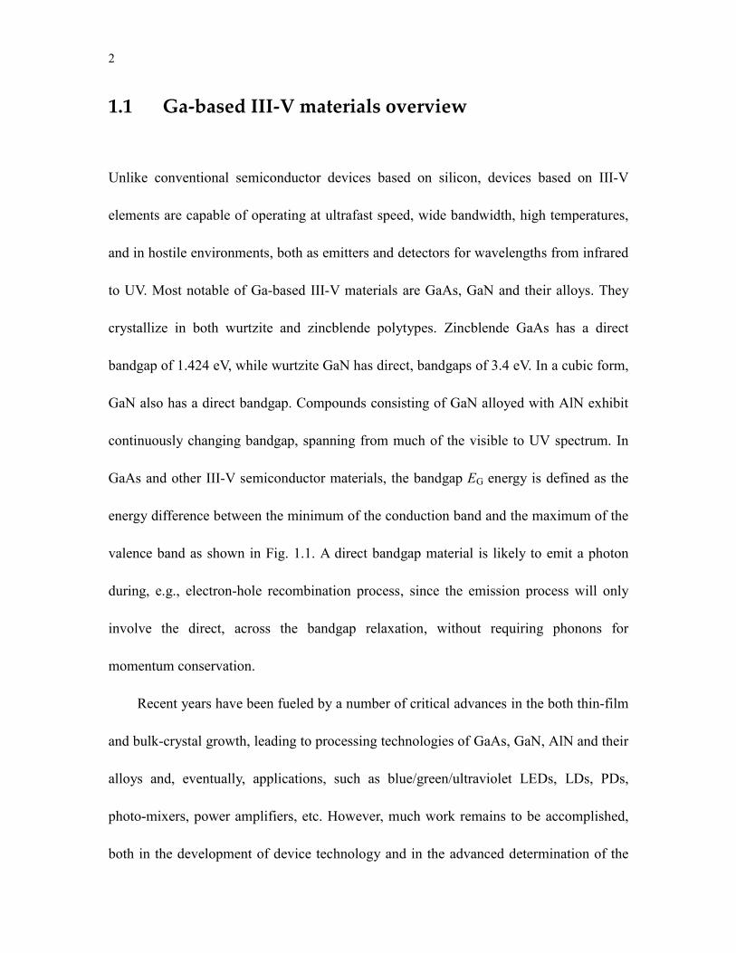
1.1 Ga-based III-V materials overview
Unlike conventional semiconductor devices based on silicon, devices based on III-V
elements are capable of operating at ultrafast speed, wide bandwidth, high temperatures,
and in hostile environments, both as emitters and detectors for wavelengths from infrared
to UV. Most notable of Ga-based III-V materials are GaAs, GaN and their alloys. They
crystallize in both wurtzite and zincblende polytypes. Zincblende GaAs has a direct
bandgap of 1.424 eV, while wurtzite GaN has direct, bandgaps of 3.4 eV. In a cubic form,
GaN also has a direct bandgap. Compounds consisting of GaN alloyed with AlN exhibit
continuously changing bandgap, spanning from much of the visible to UV spectrum. In
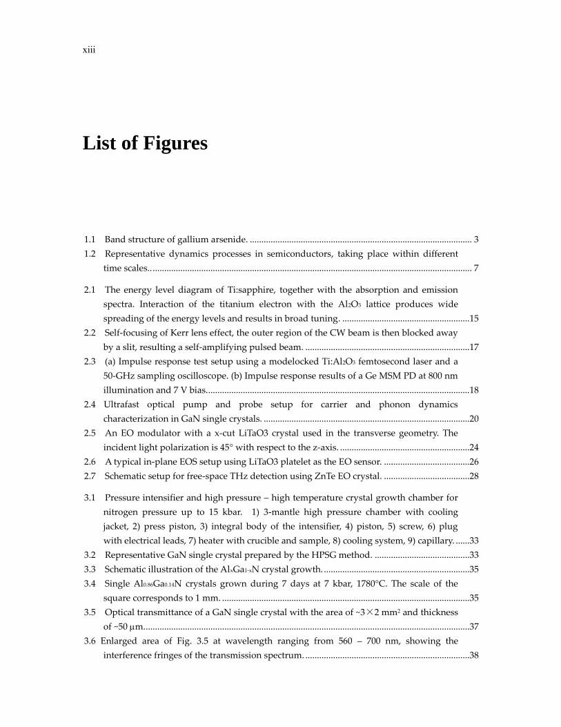
GaAs and other III-V semiconductor materials, the bandgap EG energy is defined as the
energy difference between the minimum of the conduction band and the maximum of the
valence band as shown in Fig. 1.1. A direct bandgap material is likely to emit a photon
during, e.g., electron-hole recombination process, since the emission process will only
involve the direct, across the bandgap relaxation, without requiring phonons for
momentum conservation.
Recent years have been fueled by a number of critical advances in the both thin-film
and bulk-crystal growth, leading to processing technologies of GaAs, GaN, AlN and their
alloys and, eventually, applications, such as blue/green/ultraviolet LEDs, LDs, PDs,
photo-mixers, power amplifiers, etc. However, much work remains to be accomplished,
both in the development of device technology and in the advanced determination of the
3
fundamental physical properties of such materials.
Figure 1.1 Band structure of gallium arsenide.
1.1.1 Properties of the Ga-based III-V semiconductors
GaAs is a compound of the elements gallium and arsenic and it has EG = 1.42 eV at room
temperature. Electronic properties of GaAs are superior to those of silicon. It has a higher
saturation velocity and much higher electron mobility, allowing GaAs transistors to
function at frequencies in excess of 600 GHz. [9] GaAs is the most investigated III-V
semiconductor and can also be implemented as a mid-infrared optical parametric
4
oscillator (OPO) and a THz radiation source, acting as either a photoconductive switch or
difference frequency mixer. Other applications of GaAs include: high efficiency solar
cells, infrared and X-ray detectors, and monolithic microwave integrated circuits. [10-12]
Another Ga-based III-V material of very significant importance is the GaN. It can
crystallize in both the wurtzite and zincblende forms. However, the wurtzite polytype
appears to be most extensively studied. GaN is the second most developed material of the
group and is most commonly used in III-N hetero-structures. The strongest feature of
GaN is the heterostructure technology it can support. Quantum wells, modulation-doped
hetero-interfaces, and heterojunction structures can all be made in GaN-based systems,
giving access to new spectral regions for optical devices and new operation regimes for
electronic devices. Other advantageous properties of GaN include high mechanical and
thermal stability, the large piezoelectric constants, and novel room-temperature
ferromagnetism in Mn-doped GaN crystals.
A comparison of the EG values, dielectric constant , breakdown field Fbr, saturation
velocities vsat, mobility and conductivity for GaAs, GaN, and Si is shown in Table
1.1.
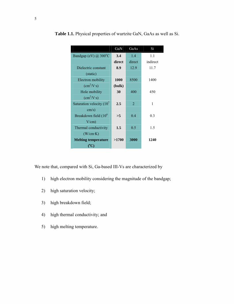
5
Table 1.1. Physical properties of wurtzite GaN, GaAs as well as Si.
GaN GaAs Si
Bandgap (eV) @ 300oC 3.4
direct
1.4 direct
1.1 indirect
Dielectric constant (static)
8.9 12.9 11.7
Electron mobility (cm2/V∙s)
1000
(bulk)
8500 1400
Hole mobility (cm2/V∙s)
30 400 450
Saturation velocity (107
cm/s) 2.5 2 1
Breakdown field (106 V/cm)
>5 0.4 0.3
Thermal conductivity (W/cm∙K)
1.5 0.5 1.5
Melting temperature
(oC)
>1700 3000 1240
We note that, compared with Si, Ga-based III-Vs are characterized by
1) high electron mobility considering the magnitude of the bandgap;
2) high saturation velocity;
3) high breakdown field;
4) high thermal conductivity; and
5) high melting temperature.
6
1.1.2 Applications for Ga-based III-V semiconductors
There are currently five major applications for the Ga-based III-V material system:
i. Solar cells and detectors;
ii. Infrared and UV optical sources;
iii. Blue and green LEDs;
iv. Power amplifiers, ultra-high-power switches, and monolithic microwave integrated
circuits (MMICs);
v. Mn-doped ferromagnetic semiconductors for spintronics.
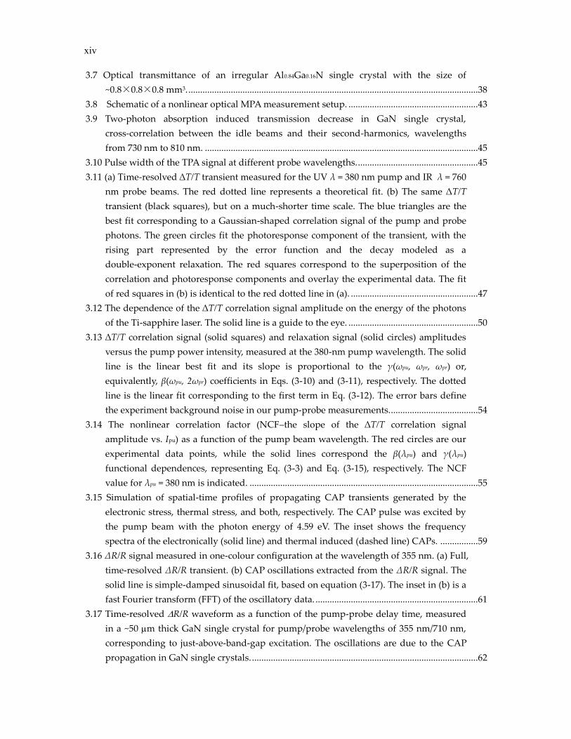
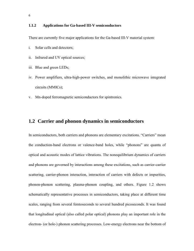
1.2 Carrier and phonon dynamics in semiconductors
In semiconductors, both carriers and phonons are elementary excitations. “Carriers” mean
the conduction-band electrons or valence-band holes, while “phonons” are quanta of
optical and acoustic modes of lattice vibrations. The nonequilibrium dynamics of carriers
and phonons are governed by interactions among these excitations, such as carrier-carrier
scattering, carrier-phonon interaction, interaction of carriers with defects or impurities,
phonon-phonon scattering, plasma-phonon coupling, and others. Figure 1.2 shows
schematically representative processes in semiconductors, taking place at different time
scales, ranging from several femtoseconds to several hundred picoseconds. It was found
that longitudinal optical (also called polar optical) phonons play an important role in the
electron- (or hole-) phonon scattering processes. Low-energy electrons near the bottom of
7
the conduction band central valley, because of their s-like wavefunctions, only interact
with longitudinal optical phonons through Fröhlich interaction. The matrix elements of
the Fröhlich interaction vary inversely with the optical phonon wave vector; thus, the
interaction is the most efficient for zone center’s polar optical phonons. Holes, which
occupy p-like states in the valence band, can interact with phonons through both polar
and non-polar coupling. Since the Fröhlich interaction rate varies as m*1/2, the heavier
holes interact more strongly with the longitudinal optical phonons than the lighter
electrons.
Figure 1.2 Representative dynamics processes in semiconductors, taking place within different time scales.
Interactions between electrons and acoustic phonons are important from both
basic-research and technological points of view. For small wavevectors near the center of
8
the Brillouin zone, the acoustic phonons have low energies and are not very efficient for
cooling of electrons. However, excited electrons can break the lattice equilibrium,
resulting in a strong deformation potential-coupled electronic stress, which is responsible
for generation of CAPs in III-Nitride materials, such as GaN single crystals.
The electron-hole pairs are created by photons hitting the crystal structure if their
energy is equal to or greater than EG. The opposite of absorption is the process of the
electron-hole pair recombination. In general, carrier recombination results from
interaction of electrons and holes, with either the lattice of the material, or with optical
photons. There are two types of recombination: radiative and nonradiative. The
nonradiative recombination occurs when excessive energy is released as phonons or as
excess kinetic energy of an additional electron and is, eventually, dissipated as heat.
Radiative recombination occurs when the excess energy is released as photons.
Photoluminescence is the result of electron-hole radiative recombination after injection of
photons on the crystal sample from an outside source, such as a laser.
The carrier recombination with no external source normally occurs at a constant rate
due to thermal equilibrium. When a semiconductor is pumped by an outside source, such
as a continuous wave (CW) laser, a new equilibrium is established where the
electron-hole recombination rate is a constant. The excess electrons decay back to the
valence band at a rate following exp(−t/τ), where, τ is the lifetime of the carriers. In the
simpliest form, the total carrier lifetime for radiative and nonradiactive recombination is
9
1 1 1
r nr (1-1)
where, τr, is the radiative lifetime and, τnr, is the nonradiative lifetime.
My studies focus on the physics of ultrafast carrier and phonon dynamics, such as,
one and/or multiple photon absorption, generation and propagation of CAPs, as well as
the electron-hole recombination rate in Ga-based III-V materials.
1.3 Thesis outline
This thesis is focused on carrier and phonon dynamics in GaN and AlGaN single crystals,
investigated by the femtosecond pump-probe spectroscopy, as well as the ultrafast
characterization of epitaxially-grown single-crystal meso-structured and self-switching
GaAs devices as the novel PDs and THz emitters. The remainder of the thesis is arranged
in four chapters.
In Chapter 2, we introduce our femtosecond mode-locked laser system. Then, our
experimental techniques implemented for time-resolved characterization of Ga-based
III-Vs are presented. The experimental approaches include: impulse response
measurement, pump-probe spectroscopy, in-plane electro-optic (EO) sampling, and
free-space time-domain THz spectroscopy.
In Chapter 3, we first briefly outline a high-pressure, high temperature, solution
10
growth method used at the ETH Zurich for the preparation of GaN and AlGaN single
crystals used in our experiments. Next, detailed studies of MPA process and nonlinear
correlation-factor in GaN and AlGaN single crystals are presented. After the introduction
of the NLO processes in III-Nitrides, we focus on the generation, detection, and lifetime
determination of CAPs in GaN single crystals. Finally, device applications of GaN
materials, such as metal-semiconductor-metal (MSM) PDs and optoelectronic integrated
circuit (OEICs) are presented.
Chapter 4 concentrates on characterization of a novel nano-optoelectronic device
based on epitaxially-grown, single crystal GaAs, called a freestanding PD. Basic
properties of the freestanding GaAs meso-structured detectors (the dark current,
responsivity and detection efficiency) are investigated and reviewed. Our time-resolved
EO sampling results show that these devices feature a 3-dB bandwidth of 1.4 THz as well
as a working repetition rate of ~ 1 THz – the most promising high speed, high repetition
rate detector of choice. Freestanding GaAs meso-structures characterized in this chapter
were fabricated at the Jülich Research Center, Jülich, Germany.
Another novel nano-device, a so-called self-switching device is introduced in
Chapter 5. We start with the DC characteristics and impulse response measurements of
the device. With the help of time-resolved EO sampling system, we detected, for the first
time, transient THz radiation bursts generated by the DC-biased SSD. The SSDs for this
study were fabricated at the University of Manchester, Manchester, UK, are provided to
us by collaboration with the University of Salamanca, Salamanca, Spain.

11
Finally, in Chapter 6, we summarize our accomplishments and suggest some further
investigations.
12
Bibliography
[1] S. Wu, P. Geiser, J. Jun, J. Karpinski and R. Sobolewski, Phys. Rev. B 76, 085210
(2007).
[2] X. Zheng, Y. Xu, R. Sobolewski, R. Adam, M. Mikulics, M. Siegel and P. Kordos,
Appl. Optics, 42(9), 1726 (2003).
[3] S. Wu, J. Zhang, A. Belousov, J. Karpinski, and R. Sobolewski, Proc. of SPIE, 6894,
68940K, (2008).
[4] G. Imeshev, M. E. Fermann, K. L. Vodopyanov, M. M. Fejer, X. Yu, J. S. Harris, D.
Bliss, and C. Lynch, Optics Express, 14, 4439 (2006).
[5] S. J. Pearton, J. C. Zolper, R. J. Shul and F. Ren, J. Appl. Phys., 86, 1 (1999).
[6] M. Mikulics, P. Kordoš, D. Gregušová, R. Adam, Martin Kočan, S. Wu, J. Zhang, R.
Sobolewski, D. Grützmacher, and M. Marso, IEEE Phot. Tech. Lett. 23, 17, (2011).
[7] S. Nakamura, et. al., Jpn. J. Appl. Phys. 36 1568 (1997).
[8] S. Nakamura, et. al., Jpn. J. Appl. Phys. 37 1020 (1998).
[9] A. Lisauskas, G. Johann Wolfgang, W. Frankfurt von Spiegel, S. Boubanga-Tombet,
A. El Fatimy, D. Coquillat, F. Teppe, N. Dyakonova, W. Knap, H. G. Roskos, IEEE
electron letters, 44, 408, (2008).
13
[10] E. Ortiz, I. Rey-Stolle, V. Diaz, R. Pena, V. M. Andreev, V. P. Khvostikov, V. D.
Rumyantsev, IEEE trans on Electron Device, 48, 840 (2001).
[11] E. Bertolucci, M.G. Bisogni, U. Bottigli, A. Cola, M.E. Fantacci, V. Rosso, A.
Stefanini, L. Vasanelli, Nuclear Instruments and Methods in Physics Research
Section A: Accelerators, Spectrometers, Detectors and Associated Equipment, 362,
547 (1995).
[12] B. Thomas, C. Lee, A. Peralta, J. Gill, G. Chattopadhyay, S. Sin, R. Lin and I. Mehdi,
“A 530-600 GHz silicon micro-machined integrated receiver using GaAs MMIC
membrane planar Schottky diodes”, 21st international symposium on space terahertz
technology, OXFORD, 23-25 March, 2010
14
2. Experimental techniques
In this chapter, I describe experimental techniques for characterization of Ga-based III-V
semiconductor materials and related devices. All our experimental results presented in
Chapters 3, 4, and 5 were obtained by the following experimental techniques: impulse
response measurements, time-resolved pump-probe spectroscopy, in-plane EO sampling
and free-space THz spectroscopy. Since in all experiments, the “centerpiece” has been the
femtosecond laser system, I start with its brief introduction followed by related
time-resolved sampling techniques.
2.1. Mode-locked femtosecond laser system
The self-modelocked femtosecond Ti:sapphire oscillator (MIRA, Coherent) is one of the
most commonly used commercial short-pulsed lasers. The Ti:sapphire laser typically
generates an average optical power of 1.6 W when pumped by a 10 W CW, green (532
nm) laser (Verdi, Coherent). It features a 100-fs pulse width and very broadly tunable
wavelength spectrum ranging from 600 nm range up to about 1050 nm. Such wide
emitting spectrum is a result of band splitting due to distortion in the lattice by Ti+3
15
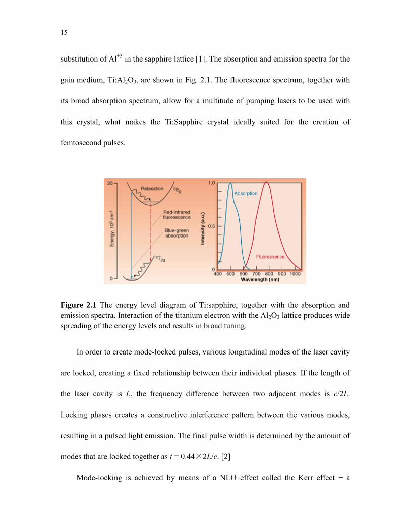
substitution of Al+3 in the sapphire lattice [1]. The absorption and emission spectra for the
gain medium, Ti:Al2O3, are shown in Fig. 2.1. The fluorescence spectrum, together with
its broad absorption spectrum, allow for a multitude of pumping lasers to be used with
this crystal, what makes the Ti:Sapphire crystal ideally suited for the creation of
femtosecond pulses.
Figure 2.1 The energy level diagram of Ti:sapphire, together with the absorption and emission spectra. Interaction of the titanium electron with the Al2O3 lattice produces wide spreading of the energy levels and results in broad tuning.
In order to create mode-locked pulses, various longitudinal modes of the laser cavity
are locked, creating a fixed relationship between their individual phases. If the length of
the laser cavity is L, the frequency difference between two adjacent modes is c/2L.
Locking phases creates a constructive interference pattern between the various modes,
resulting in a pulsed light emission. The final pulse width is determined by the amount of
modes that are locked together as t = 0.44×2L/c. [2]
Mode-locking is achieved by means of a NLO effect called the Kerr effect − a
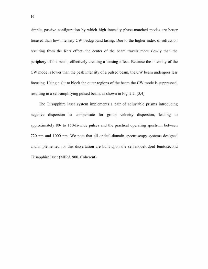
16
simple, passive configuration by which high intensity phase-matched modes are better
focused than low intensity CW background lasing. Due to the higher index of refraction
resulting from the Kerr effect, the center of the beam travels more slowly than the
periphery of the beam, effectively creating a lensing effect. Because the intensity of the
CW mode is lower than the peak intensity of a pulsed beam, the CW beam undergoes less
focusing. Using a slit to block the outer regions of the beam the CW mode is suppressed,
resulting in a self-amplifying pulsed beam, as shown in Fig. 2.2. [3,4]
The Ti:sapphire laser system implements a pair of adjustable prisms introducing
negative dispersion to compensate for group velocity dispersion, leading to
approximately 80- to 150-fs-wide pulses and the practical operating spectrum between
720 nm and 1000 nm. We note that all optical-domain spectroscopy systems designed
and implemented for this dissertation are built upon the self-modelocked femtosecond
Ti:sapphire laser (MIRA 900, Coherent).
17
Figure 2.2 Self-focusing of Kerr lens effect, the outer region of the CW beam is then blocked away by a slit, resulting a self-amplifying pulsed beam.
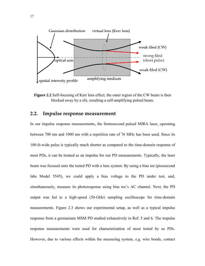
2.2. Impulse response measurement
In our impulse response measurements, the femtosecond pulsed MIRA laser, operating
between 700 nm and 1000 nm with a repetition rate of 76 MHz has been used. Since its
100-fs-wide pulse is typically much shorter as compared to the time-domain response of
most PDs, it can be treated as an impulse for our PD measurements. Typically, the laser
beam was focused onto the tested PD with a lens system. By using a bias tee (pisosecond
labs Model 5545), we could apply a bias voltage to the PD under test, and,
simultaneously, measure its photoresponse using bias tee’s AC channel. Next, the PD
output was fed to a high-speed (50-GHz) sampling oscilloscope for time-domain
measurements. Figure 2.3 shows our experimental setup, as well as a typical impulse
response from a germanium MSM PD studied exhaustively in Ref. 5 and 6. The impulse
response measurements were used for characterization of most tested by us PDs.
However, due to various effects within the measuring system, e.g. wire bonds, contact
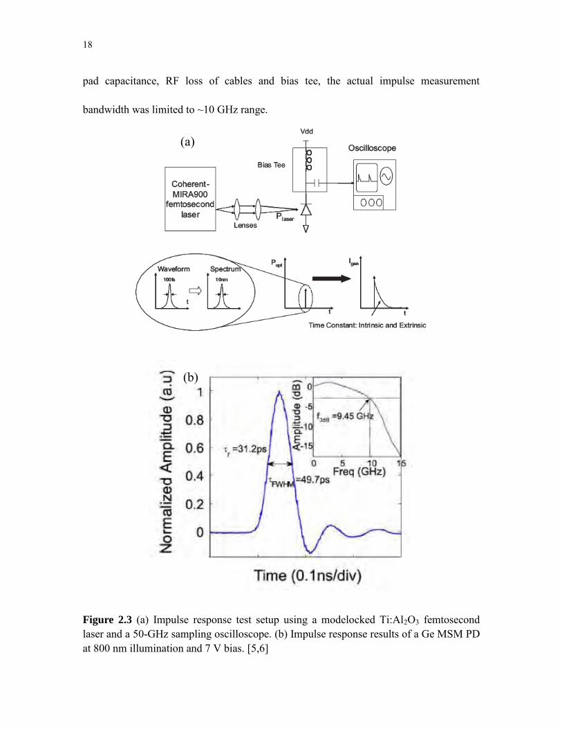
18
pad capacitance, RF loss of cables and bias tee, the actual impulse measurement
bandwidth was limited to ~10 GHz range.
Figure 2.3 (a) Impulse response test setup using a modelocked Ti:Al2O3 femtosecond laser and a 50-GHz sampling oscilloscope. (b) Impulse response results of a Ge MSM PD at 800 nm illumination and 7 V bias. [5,6]
(a)
(b)
19
2.3. Time-resolved femtosecond pump-probe spectroscopy
Femtosecond pump-probe spectroscopy is a very useful tool for investigation of ultrafast
(sub-picosecond to a few nanoseconds) nonequilibrium carrier dynamics in
condensed-matter materials. Figure 2.4 presents our femtosecond optical pump-probe
setup for carrier and phonon dynamics characterization in III-Nitrides. Both one-color
and two-color pump-probe spectroscopy experiments can be performed in reflection
mode, using our MIRA oscillator, as well as homemade third- and second-harmonic
generators. In the two-color version, UV pulses with the width of ~150 fs and photon
energies ranging from 4.71 to 4.42 eV and 3.53 to 3.43 eV, respectively, were used as the
pump and focused on the sample surface with a spot diameter of ~20 µm, the incident
angle of ~30º, and the fluence of ~0.04 mJ/cm2 per pulse. The probe pulses were either
near-infrared light, directly generated by MIRA, or UV light after passing the
second-harmonic generator. The probe pulses were aimed perpendicular to the sample
surface, had the width of ~100 fs, and their fluence was always much smaller (at least of
the factor of 10) than that of the pump.
20
Figure 2.4 Ultrafast optical pump and probe setup for carrier and phonon dynamics characterization in GaN single crystals.
The one-color pump-probe spectroscopy is also called degenerate pump-probe, and,
in this configuration, the pump excites, e.g., free electrons from the valence band to a
certain state in the conduction band, while the probe monitors the electron density change
of the same state. In the two-color pump-probe, or non-degenerate pump-probe, one
simultaneously uses two laser beams at different wavelengths (colors), which either come
from two synchronized lasers, or one beam is generated by a nonlinear frequency
conversion of the other one from the same laser source. In our work, we utilize an
above-bandgap pump and below-bandgap probe experimental configurations. In such
arrangement, the probe photons monitor the total, photo-excited population of electrons
in the entire conduction band. As indicated in Refs. 7 and 8, for the below-bandgap probe
beam, the refractive index change n is purely induced by the photoexcited electron-hole
plasma and can be described by the simple Drude model, which expresses n as
21
*20
22/mNenn
, (2-1)
where n is the refractive index of the sample at the probe wavelength, 0 is the
background dielectric constant at low frequencies, e is the unit electronic charge, is the
probe angular frequency, and N and m* are the electron density and the effective mass in
the conduction band, respectively. The contribution of holes to n is neglected, because
holes typically have a much heavier effective mass than electrons. Equation (2-1) shows
that n changes linearly with the density N of conduction-band electrons.
For pump-probe spectroscopy performed in the reflection mode (in particular, our
coherent phonon measurements), it is essential to show how the experimental probe-beam
differential reflectivity R/R is related to N. The definition of R/R is
R
RRRR
'/ , (2-2)
where R’ and R represent the probe beam reflectivity in the presence and absence of the
pump beam, respectively. For thick samples, R at the normal incidence is defined as
21 1R n n . (2-3)
22
Since R is only dependent on n, one can write normalized change in the reflectivityR/R
as
ndnRdRR /)(ln/ . (2-4)
By substituting Eq. (2-1) into the above equation, one can obtain the relationship between
R/R and N which is expressed as
*20
2 )(ln2/mN
dnRdenRR
. (2-5)
Equation (2-5) shows that R/R is linearly related to N. Therefore, the time-resolved,
experimental R/R signal directly gives the time evolution of N in the conduction band
and does not depend on the details of the electronic states.
In CAP experiments, we measured the time-resolved normalized change in the
reflectivity ΔR/R of the probe-beam over a time-delay window of ~500 ps. The UV pump
pulses absorbed at the crystal surface generated the thermal and/or electronic stress and
triggered a strain transient (CAP pulse), which, while propagating inside the sample,
modulated its local n, leading to the ΔR/R signal, detected by the delayed probe pulses.
We also utilized pump-probe spectroscopy for the study of MPA process in
III-Nitrides. The ultrafast correlation type MPA studies involved two laser beams, i.e.,
23
pump and probe, both having below bandgap wavelengths. The MPA study has been a
valuable tool for us investigating the NLO properties of III-Nitrides, optical power
limitation in nitride based optoelectronics and moreover, it was a useful method for
optical pulse-width characterization. [9,10]
2.4. Transient THz electro-optic sampling
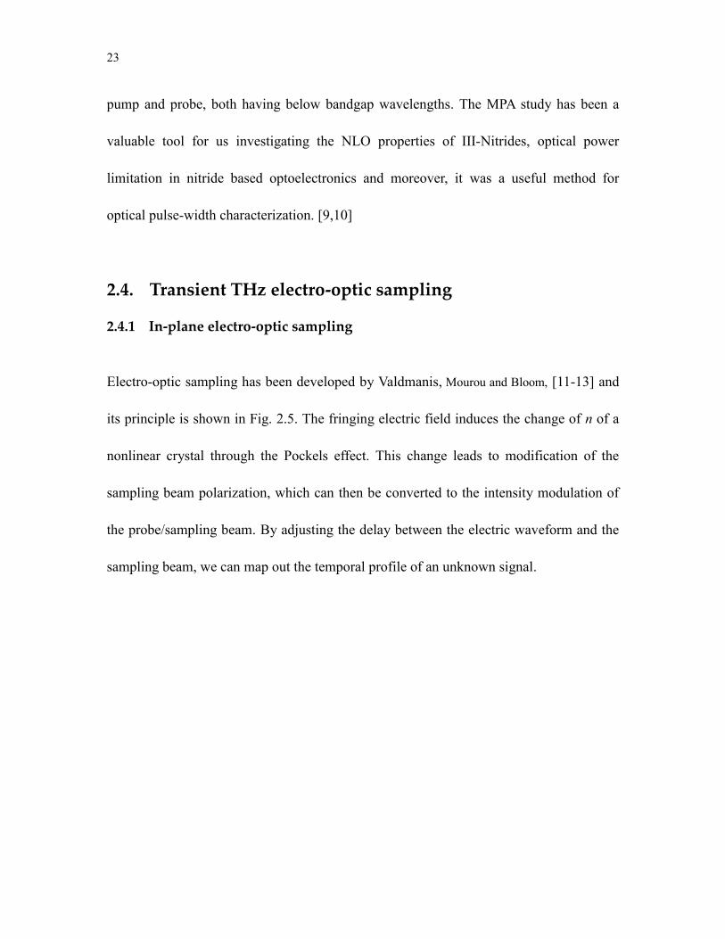
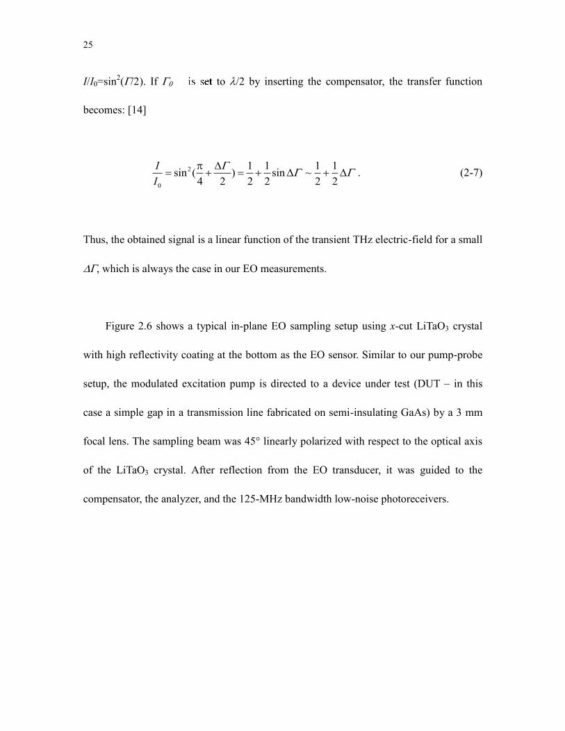
2.4.1 In-plane electro-optic sampling
Electro-optic sampling has been developed by Valdmanis, Mourou and Bloom, [11-13] and
its principle is shown in Fig. 2.5. The fringing electric field induces the change of n of a
nonlinear crystal through the Pockels effect. This change leads to modification of the
sampling beam polarization, which can then be converted to the intensity modulation of
the probe/sampling beam. By adjusting the delay between the electric waveform and the
sampling beam, we can map out the temporal profile of an unknown signal.
24
Figure 2.5 An EO modulator with a x-cut LiTaO3 crystal used in the transverse geometry. The incident light polarization is 45o with respect to the z-axis.
The Pockels effect induces an optical retardation of the polarized sampling beam.
For an x-cut LiTaO3 crystal, this phase retardation is given by: [12]
3 30 33 13
2 ( ) ( )e o e o THzn n d n r n r E L
, (2-6)
where is the sampling beam’s wavelength, d is the thickness of LiTaO3, ETHz is the
THz electric field and L is the length of region where the electric field and the light wave
overlap. The first term gives a static retardation caused by the crystal anisotropy, while
the second term describes the electric field induced by the Pockels effect. The transfer
function of the modulator can be expressed as a function of the phase retardation , by
25
I/I0=sin2(). If to /2 by inserting the compensator, the transfer function
becomes: [14]
2
0
1 1 1 1sin ( ) sin ~4 2 2 2 2 2
II
. (2-7)
Thus, the obtained signal is a linear function of the transient THz electric-field for a small
, which is always the case in our EO measurements.
Figure 2.6 shows a typical in-plane EO sampling setup using x-cut LiTaO3 crystal
with high reflectivity coating at the bottom as the EO sensor. Similar to our pump-probe
setup, the modulated excitation pump is directed to a device under test (DUT – in this
case a simple gap in a transmission line fabricated on semi-insulating GaAs) by a 3 mm
focal lens. The sampling beam was 45° linearly polarized with respect to the optical axis
of the LiTaO3 crystal. After reflection from the EO transducer, it was guided to the
compensator, the analyzer, and the 125-MHz bandwidth low-noise photoreceivers.
26
Figure 2.6 A typical in-plane EOS setup using LiTaO3 platelet as the EO sensor.
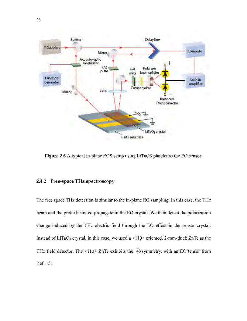
2.4.2 Free-space THz spectroscopy
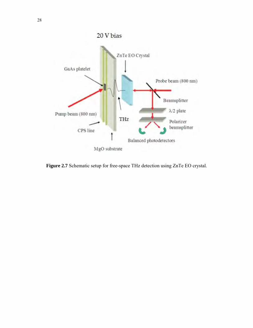
The free space THz detection is similar to the in-plane EO sampling. In this case, the THz
beam and the probe beam co-propagate in the EO crystal. We then detect the polarization
change induced by the THz electric field through the EO effect in the sensor crystal.
Instead of LiTaO3 crystal, in this case, we used a <110> oriented, 2-mm-thick ZnTe as the
THz field detector. The <110> ZnTe exhibits the 43 symmetry, with an EO tensor from
Ref. 15:
27
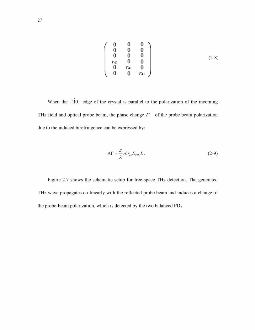
When the [110] edge of the crystal is parallel to the polarization of the incoming
THz field and optical probe beam, the phase change of the probe beam polarization
due to the induced birefringence can be expressed by:
30 41 THzn r E L
. (2-9)
Figure 2.7 shows the schematic setup for free-space THz detection. The generated
THz wave propagates co-linearly with the reflected probe beam and induces a change of
the probe-beam polarization, which is detected by the two balanced PDs.
(2-8)
28
Figure 2.7 Schematic setup for free-space THz detection using ZnTe EO crystal.
29
Bibliograghy
[1] P. F. Moulton, J. Opt. Soc. Am. B 3, 125-133 (1986).
[2] M. Fermann, A. Galvanauskas, and G. Sucha, Ultrafast Lasers: Technology and
Applications. CRC Press (2003).
[3] D. Spence, P. Kean, et al., Optics Letters 16(1), 42 (1991).
[4] J. Jin and S. Kim, Advances in Solid State Lasers Development and Applications,
INTECH, (2010).
[5] Berkehan Ciftcioglu, “Intra-Chip Free-Space Optical Interconnect: System, Device,
Integration and Prototyping”, PhD Thesis, University of Rochester, (2012).
[6] B. Ciftcioglu, J. Zhang, R. Sobolewski, and H. Wu, IEEE Phot. Tech. Lett, 20, 2069,
(2010).
[7] M. C. Downer and C. V. Shank, Phys. Rev. Lett. 56, 761 (1986).
[8] F. E. Doany and D. Grischkowsky, Appl. Phys. Lett. 52, 36 (1988).
[9] C.-K. Sun, J.-C. Liang, J.-C. Wang, F.-J. Kao, S. Keller, M. P. Mack, U. Mishra, and
Steven P. DenBaars, Appl. Phys. Lett. 76, 439 (2000).
[10] S. Krishnamurthy, K. Nashold, and A. Sher, Appl. Phys. Lett. 77, 355 (2000).
[11] J.A. Valdmanis, G.A. Mourou, and C.W. Gabel, Appl. Phys. Lett. 41,211 (1982).
[12] J. Valdmanis and G. Mourou, IEEE J. Quantum Electron., 22, 69, (1986).
30
[13] B. H. Kolner and D. M. Bloom, IEEE J. Quantum Electron. 22, 79 (1986).
[14] Xuemei Zheng, “Ultrafast characterization of optoelectronic devices and systems”,
PhD Thesis, University of Rochester, (2004).
[15] Q. Wu, M. Litz and X.-C. Zhang, Appl. Phys. Lett., 68(21), 2924, (1996).
31
3. Ultrafast carrier and phonon dynamics
in III-Nitride semiconductors
Investigations of the carrier and phonon dynamics in Ga-based III-Nitrides are of
fundamental importance in understanding nonlinear transport properties that form the
basis of III-Nitride electronic and optoelectronic devices. We all know that the
nonequilibrium dynamics of carriers is governed by interactions between carriers and
boson excitations, such as photons and/or phonons. In general, there is a variety of
interactions in semiconductors, such as the carrier-carrier scattering, carrier-phonon
interaction, the interaction of carriers with defects or impurities, phonon-phonon
interaction, plasma-phonon coupling, and so on. In this chapter, I present my studies on
the NLO process and MPA in GaN and AlGaN bulk single crystals, as well as on
generation, propagation, and detection of ultra-long-lived CAPs in GaN single crystals. I
start with the outline of preparation of GaN and AlGaN single crystals using high
pressure, high temperature, solution growth method and their optical properties.
32
3.1. III-Nitride single crystals growth
3.1.1 GaN single crystal growth
Our GaN and AlGaN single crystals were grown at Professor Karpinski’s Group at the
Solid State Physics Laboratory, ETH Zurich, Switzerland, using a high-pressure
solution-growth (HPSG) method [1,2]. Figure 3.1 schematically shows the ETH
high-temperature, high-pressure crystal growth apparatus. The growth process was
carried out at an external nitrogen gas pressure of 8-14 kbar and temperatures of 1350–
1600°C, because of high solubility of GaN in Ga at high temperatures. Nitrogen was first
compressed with a commercial compressor up to 3 kbar and then compressed up to 10-15
kbar with a pressure intensifier. The pressure intensifier chamber had an internal diameter
of 30 mm and in this chamber, the high temperature furnace with a Pt-Rh heater was
placed. Nitrogen was then transported into the metallic Ga melt with a temperature
gradient of 5-50 °C/cm. GaN single crystals formed at the cooler zone of the HPSG
chamber. They grew up to 1-mm-thick platelets with typical sizes of up to 34 mm2, as
shown in Fig. 3.2. These crystals exhibited an excellent wurtzite crystalline structure,
while their morphology depended on the growth process pressure, temperature range, and
nitrogen supersaturation. In all our experiments, we have studied several ~1.52 mm2,
transparent (slightly brownish) GaN crystal pieces, typically ~0.1 to 0.4 mm thick.
33
Figure 3.1 Pressure intensifier and high pressure – high temperature crystal growth chamber for nitrogen pressure up to 15 kbar. 1) 3-mantle high pressure chamber with cooling jacket, 2) press piston, 3) integral body of the intensifier, 4) piston, 5) screw, 6) plug with electrical leads, 7) heater with crucible and sample, 8) cooling system, 9) capillary. [1]
Figure 3.2 Representative GaN single crystal prepared by the HPSG method.
1mm
34
3.1.2 (Al,Ga)N single crystal growth
The AlxGa1-xN crystals with Al content 0.5<x<1 have been synthesized from the solution
in Ga melt in nitrogen gas in the HPSG system. [2] Figure 3.3 illustrates the schematic of
AlGaN single crystal growth. The high nitrogen gas line consisted of the compressor, the
high pressure chamber of 40 mm internal diameter with internal three zone furnace and
the electronic system for stabilizing and programming the pressure and temperature.
Using a membrane Nova Swiss gas compressor, nitrogen gas was pumped up 3 kbar into
30 mm diameter pressure intensifier and finally the pressure was transmitted and
increased up to the required value in 40 mm experimental chamber by pressure
intensifier. By using of BN isolation and W/Re heater in the furnace the maximum
temperature of about 1750-1800°C was be obtained. At such high temperature diffusion
of nitrogen into Ga melt increases. Temperature was measured by a set of 3
thermocouples placed along the crucible, which were connected to Eurotherm
programmer units. The latter allowed to precisely control both temperature and
temperature gradient in the furnace.
35
Figure 3.3 Schematic illustration of the AlxGa1-xN crystal growth. [2]
Figure 3.4 Single Al0.86Ga0.14N crystals grown during 7 days at 7 kbar, 1780°C. The scale of the square corresponds to 1 mm.
The polycrystalline AlyGa1-yN samples covering 0<y<1 composition range were used as
precursors for the AlxGa1-xN single crystal growth. They were synthesized by solid-phase
1mm
36
reaction in cubic anvil under 30 kbar pressure and 1800 °C. The starting materials were
highly pure GaN and AlN (Alfa Ceasar) powders blended with a mortar for suitable
compositions (y = 0.2, 0.4, 0.5, 0.9). The samples were filled in boron nitride crucible
placed in graphite cylinder that served as a furnace, heated for 3 hours and finally cooled
down to room temperature. The pressure medium was pyrophilite. Sintered samples have
a diameter of about 6 mm and 4 mm length.
The precursor pellet was placed in the Ga melt in the upper part of the graphite
crucible in the gas pressure chamber (see Fig. 3.3). The graphite crucible has an internal
diameter of 14 mm and 70 mm length. The total concentration of aluminum in Ga melt
did not exceed 1 wt%. By applying of the constant thermal gradient, the AlxGa1-xN
crystals grew in the colder part of the graphite crucible. In order to prevent the growth of
GaN crystals the applied pressure and temperature during the synthesis were outside of
the stable growth region for GaN phase. Especially, it was very important during the
cooling phase at the end of the process. AlxGa1-xN crystals were typically grown in a
constant thermal gradient of about 20K/cm during 6-7 days. Figure 3.4 shows a picture of
AlGaN single crystals, their sizes are up to 0.8×0.8×0.8 mm3.
3.2. Optical properties of III-Nitrides
The optical transmittance of our GaN and AlGaN samples was measured by us using a
Perkin-Elmer Lambda 900 spectrophotometer at normal incidence by scanning the
wavelength from 200 nm to 850 nm.
37
Figure 3.5 Optical transmittance of a GaN single crystal with the area of ~3×2 mm2 and thickness of ~50 m.
For GaN single crystals, a typical result is shown in Fig. 3.5. As we can see, the UV
to visible contrast is more than 3 decades (at 300 nm the reading is about 0.01%, the limit
of the instrument; at 700 nm the reading is about 60%). We also note that, since our GaN
plate is high quality and very thin, the plate thickness can be accurately calculated from a
simple transmittance spectrum using Swanepoel method. [3]
When plate thickness is uniform, interference effects give rise to the typical
transmittance spectrum with successive maxima and minima (see Fig. 3.6). Then, the film
thickness can be obtained from the refractive index corresponding to adjacent extreme
values, n1= n (1) and n2= n (2) through the following expression:
38
1 2
1 2 2 12( )d M
n n
(3-1)
where M = 1 for two adjacent maxima (or minima), leading to d = 52 m.
Figure 3.6 Enlarged area of Fig. 3.5 at wavelength ranging from 560 – 700 nm, showing the interference fringes of the transmission spectrum.
Figure 3.7 Optical transmittance of an irregular Al0.84Ga0.16N single crystal with the size of ~0.8×0.8×0.8 mm3.
39
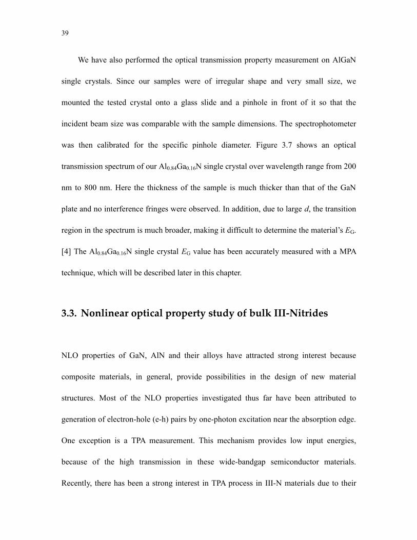
We have also performed the optical transmission property measurement on AlGaN
single crystals. Since our samples were of irregular shape and very small size, we
mounted the tested crystal onto a glass slide and a pinhole in front of it so that the
incident beam size was comparable with the sample dimensions. The spectrophotometer
was then calibrated for the specific pinhole diameter. Figure 3.7 shows an optical
transmission spectrum of our Al0.84Ga0.16N single crystal over wavelength range from 200
nm to 800 nm. Here the thickness of the sample is much thicker than that of the GaN
plate and no interference fringes were observed. In addition, due to large d, the transition
region in the spectrum is much broader, making it difficult to determine the material’s EG.
[4] The Al0.84Ga0.16N single crystal EG value has been accurately measured with a MPA
technique, which will be described later in this chapter.
3.3. Nonlinear optical property study of bulk III-Nitrides
NLO properties of GaN, AlN and their alloys have attracted strong interest because
composite materials, in general, provide possibilities in the design of new material
structures. Most of the NLO properties investigated thus far have been attributed to
generation of electron-hole (e-h) pairs by one-photon excitation near the absorption edge.
One exception is a TPA measurement. This mechanism provides low input energies,
because of the high transmission in these wide-bandgap semiconductor materials.
Recently, there has been a strong interest in TPA process in III-N materials due to their
40
very wide bandgap. [5] TPA is a valuable method to generate low carrier densities within
large sample volume for investigations of bulk features of wide-EG semiconductors.
3.3.1 Degenerate and non-degenerate two-photon absorption
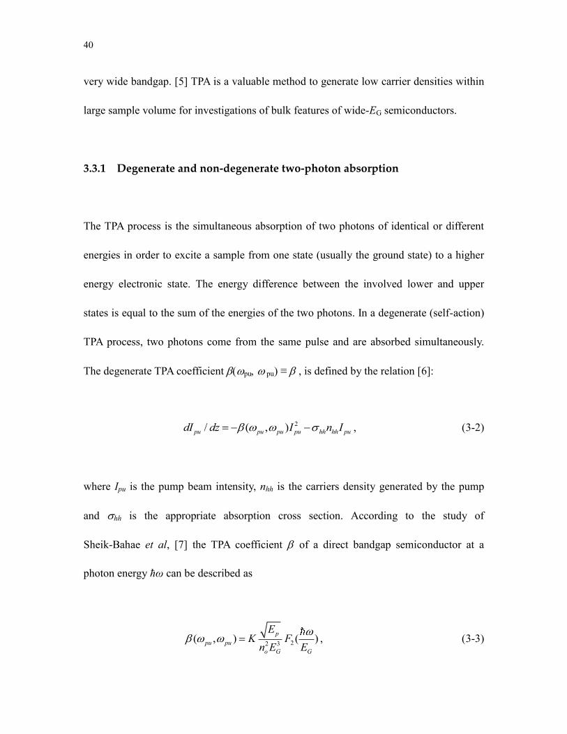
The TPA process is the simultaneous absorption of two photons of identical or different
energies in order to excite a sample from one state (usually the ground state) to a higher
energy electronic state. The energy difference between the involved lower and upper
states is equal to the sum of the energies of the two photons. In a degenerate (self-action)
TPA process, two photons come from the same pulse and are absorbed simultaneously.
The degenerate TPA coefficient pu pu≡ ,is defined by the relation [6]:
2/ ( , )pu pu pu pu hh hh pudI dz I n I , (3-2)
where Ipu is the pump beam intensity, nhh is the carriers density generated by the pump
and hh is the appropriate absorption cross section. According to the study of
Sheik-Bahae et al, [7] the TPA coefficient of a direct bandgap semiconductor at a
photon energy ћω can be described as
22 3( , ) ( )ppu pu
o G G
EK F
n E E
, (3-3)
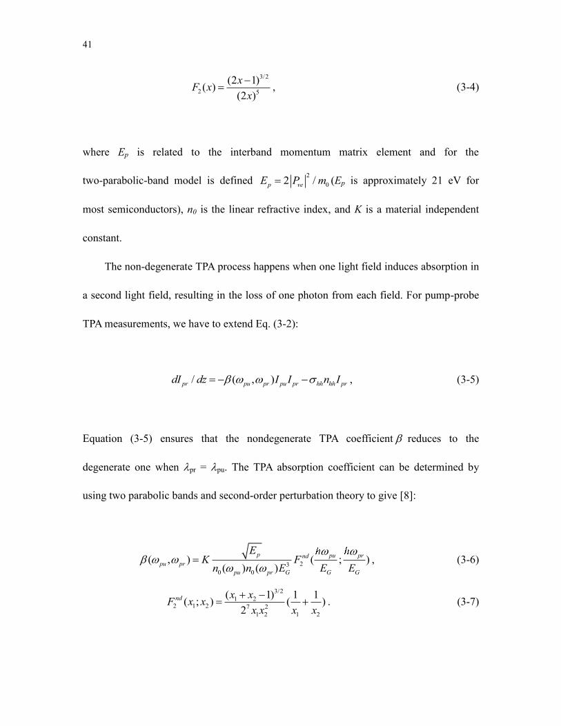
41
3/2
2 5
(2 1)( )(2 )xF x
x
, (3-4)
where Ep is related to the interband momentum matrix element and for the
two-parabolic-band model is defined 202 /p veE P m (Ep is approximately 21 eV for
most semiconductors), n0 is the linear refractive index, and K is a material independent
constant.
The non-degenerate TPA process happens when one light field induces absorption in
a second light field, resulting in the loss of one photon from each field. For pump-probe
TPA measurements, we have to extend Eq. (3-2):
/ ( , )pr pu pr pu pr hh hh prdI dz I I n I , (3-5)
Equation (3-5) ensures that the nondegenerate TPA coefficientreduces to the
degenerate one when pr = pu. The TPA absorption coefficient can be determined by
using two parabolic bands and second-order perturbation theory to give [8]:
230 0
( , ) ( ; )( ) ( )
p pu prndpu pr
pu pr G G G
EK F
n n E E E
, (3-6)
3/21 2
2 1 2 7 21 2 1 2
( 1) 1 1( ; ) ( )2
nd x xF x xx x x x
. (3-7)
42
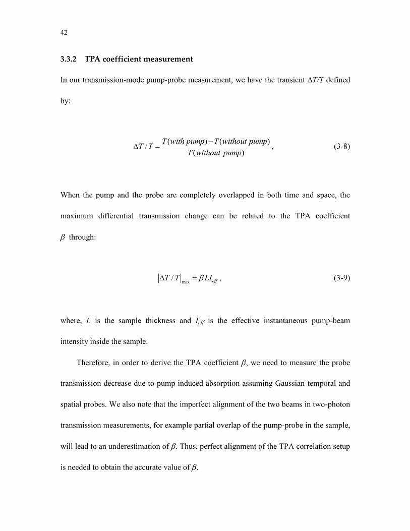
3.3.2 TPA coefficient measurement
In our transmission-mode pump-probe measurement, we have the transient ∆T/T defined
by:
( ) ( )/( )
T with pump T without pumpT TT without pump
, (3-8)
When the pump and the probe are completely overlapped in both time and space, the
maximum differential transmission change can be related to the TPA coefficient
through:
max/ effT T LI , (3-9)
where, L is the sample thickness and Ieff is the effective instantaneous pump-beam
intensity inside the sample.
Therefore, in order to derive the TPA coefficient , we need to measure the probe
transmission decrease due to pump induced absorption assuming Gaussian temporal and
spatial probes. We also note that the imperfect alignment of the two beams in two-photon
transmission measurements, for example partial overlap of the pump-probe in the sample,
will lead to an underestimation of . Thus, perfect alignment of the TPA correlation setup
is needed to obtain the accurate value of .
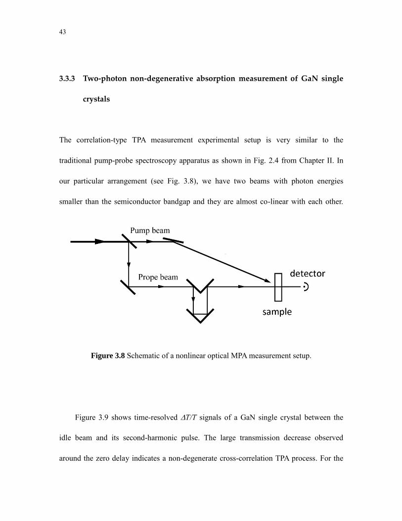
43
3.3.3 Two-photon non-degenerative absorption measurement of GaN single
crystals
The correlation-type TPA measurement experimental setup is very similar to the
traditional pump-probe spectroscopy apparatus as shown in Fig. 2.4 from Chapter II. In
our particular arrangement (see Fig. 3.8), we have two beams with photon energies
smaller than the semiconductor bandgap and they are almost co-linear with each other.
Figure 3.8 Schematic of a nonlinear optical MPA measurement setup.
Figure 3.9 shows time-resolved T/T signals of a GaN single crystal between the
idle beam and its second-harmonic pulse. The large transmission decrease observed
around the zero delay indicates a non-degenerate cross-correlation TPA process. For the
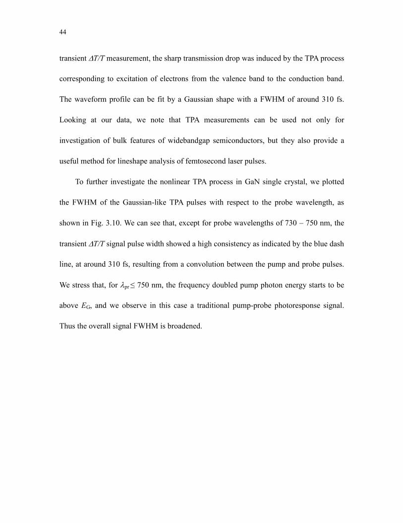
44
transient T/T measurement, the sharp transmission drop was induced by the TPA process
corresponding to excitation of electrons from the valence band to the conduction band.
The waveform profile can be fit by a Gaussian shape with a FWHM of around 310 fs.
Looking at our data, we note that TPA measurements can be used not only for
investigation of bulk features of widebandgap semiconductors, but they also provide a
useful method for lineshape analysis of femtosecond laser pulses.
To further investigate the nonlinear TPA process in GaN single crystal, we plotted
the FWHM of the Gaussian-like TPA pulses with respect to the probe wavelength, as
shown in Fig. 3.10. We can see that, except for probe wavelengths of 730 – 750 nm, the
transient T/T signal pulse width showed a high consistency as indicated by the blue dash
line, at around 310 fs, resulting from a convolution between the pump and probe pulses.
We stress that, for pr ≤ 750 nm, the frequency doubled pump photon energy starts to be
above EG, and we observe in this case a traditional pump-probe photoresponse signal.
Thus the overall signal FWHM is broadened.
45
Figure 3.9 Two-photon absorption induced transmission decrease in GaN single crystal, cross-correlation between the idle beams and their second-harmonics, wavelengths from 730 nm to 810 nm.
Figure 3.10 Pulse width of the TPA signal at different probe wavelengths.
46
3.3.4 Multi-photon absorption measurement of bulk (Al,Ga)N single crystals
We have also performed the two-color pump-probe measurements on (Al,Ga)N single
crystals. Figure 3.11 presents a typical time-resolved ∆T/T transient vs. probe delay time
relative to the pump, obtained by exciting the AlGaN crystal with 380-nm pump and
760-nm probe beams. The ∆T/T waveform was averaged 4 times, resulting that the noise
floor our measurements was below 0.1×10⁻⁴. Figure 3.11(a) depicts the full transient in a
long-time window, and the dotted line is a numerical fit, which will be described later.
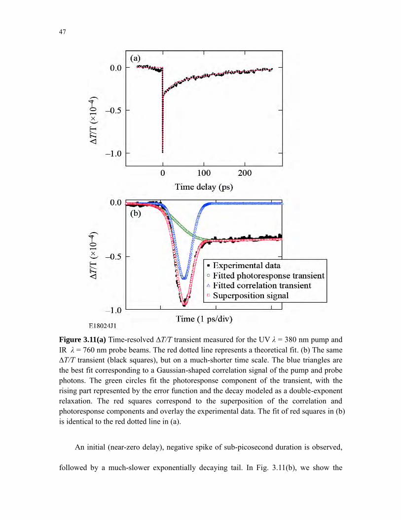
47
Figure 3.11(a) Time-resolved ∆T/T transient measured for the UV λ = 380 nm pump and IR λ = 760 nm probe beams. The red dotted line represents a theoretical fit. (b) The same ∆T/T transient (black squares), but on a much-shorter time scale. The blue triangles are the best fit corresponding to a Gaussian-shaped correlation signal of the pump and probe photons. The green circles fit the photoresponse component of the transient, with the rising part represented by the error function and the decay modeled as a double-exponent relaxation. The red squares correspond to the superposition of the correlation and photoresponse components and overlay the experimental data. The fit of red squares in (b) is identical to the red dotted line in (a).
An initial (near-zero delay), negative spike of sub-picosecond duration is observed,
followed by a much-slower exponentially decaying tail. In Fig. 3.11(b), we show the
48
same waveform (solid squares), but on a much-shorter (<3 ps) time scale. The
experimental ∆T/T transient in Fig. 3.11(b) can be very accurately decomposed into a
Gaussian-shaped pulse (open triangles) of FWHM of 310 fs, and a second transient (open
circles) consisting of a ~0.6-ps-long rise (modeled as the error function) and an
exponential decay that is slow [on the time scale of Fig. 3.11(b)]. The superposition of the
above two transients (open squares) fits our experimental data extremely well [see also
the dotted line in Fig. 3.11(a), which represents the same fit].
Based on our decomposition procedure, we interpret the ultrafast Gaussian pulse as a
photon correlation signal since the 310-fs FWHM coincides well with the overlap of our
~150-fs-wide UV and IR pulses. The second component of the experimental ∆T/T
transient [open circles in Fig. 3.11(b)] is a probe transmission signal and it represents the
well-studied relaxation dynamics of photo-excited carriers in semiconductors [9]. On a
long time scale, the relaxation signal can be fitted [Fig. 3.11(a) (dotted line)] as a
bi-exponential decay with an initial 12 ps time constant, followed by a slow, ~130 ps
relaxation. The 12 ps decay corresponds to the initial electron–optical phonon relaxation
process within the conduction band, while the ~130 ps time constant is the carrier
lifetime, which in our AlGaN crystal is most likely dominated by the indirect,
non-radiative recombination process and carrier trapping.
The near zero-delay correlation signal was been observed only when both the pump
and probe photons were simultaneously incident on the sample. Furthermore, the
amplitude of this correlation signal is strongly dependent on the photon energy of the two
49
beams. Figure 3.12 shows the amplitude of this correlation signal as a function of the
Ti-sapphire laser photon energy (which is equal to the probe photon energy or,
equivalently, half of the pump photon energy). As can be seen in Fig. 3.12, there is a
strong threshold corresponding to a laser energy of ~1.45 eV (1.45 eV probe, 2.9 eV
pump). We interpret this threshold as the onset of a multi-photon, band-to-band
absorption process consisting of a combination of pump and probe photons. This would
require that, at the threshold, the combination of pump and probe photons would have a
total energy equal to EG of the AlGaN sample, estimated in [5] to be 5.74 eV. The only
combination (at threshold) of pump and probe photons that gives a total energy near that
of the bandgap is 1 pump photon plus 2 probe photons, giving a total energy of ~5.8 eV,
in good agreement with the estimated EG of the sample. A more precise value of EG is
obtained by performing a linear fit of the data of Fig. 3.12, producing EG = 5.81±0.3 eV
(the error is based on the spectral width of our laser pulses).
Thus, the correlation signal is produced by a band-to-band absorption process
involving 1 pump photon and 2 probe photons. This multi-photon process could simply
be 3 photon absorption (3PA), or could be a 2 photon absorption (TPA) process involving
1 pump photon and a second photon produced by SHG from 2 probe photons. As
described below, modeling of these TPA and 3PA processes predict different
dependencies on pump wavelength, thereby enabling us to experimentally determine
which of these processes is dominant.
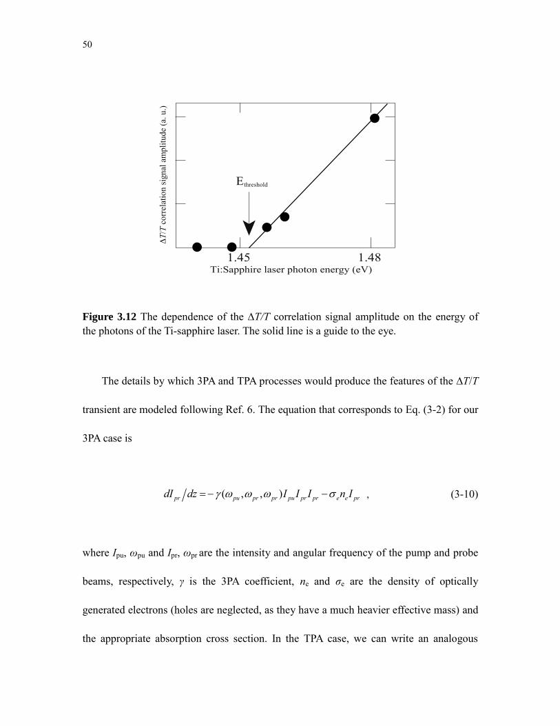
50
Figure 3.12 The dependence of the ∆T/T correlation signal amplitude on the energy of the photons of the Ti-sapphire laser. The solid line is a guide to the eye.
The details by which 3PA and TPA processes would produce the features of the ∆T/T
transient are modeled following Ref. 6. The equation that corresponds to Eq. (3-2) for our
3PA case is
, (3-10)
where Ipu, ωpu and Ipr, ωpr are the intensity and angular frequency of the pump and probe
beams, respectively, γ is the 3PA coefficient, ne and σe are the density of optically
generated electrons (holes are neglected, as they have a much heavier effective mass) and
the appropriate absorption cross section. In the TPA case, we can write an analogous
threshold
Ti:Sapphire laser photon energy (eV)
ΔT
/T c
orre
latio
n si
gnal
am
plitu
de (a
. u.)
1.45 1.48
E
( , , ) pr pu pr pr pu pr pr e e prdI dz I I I n I
51
expression:
, (3-11)
where η is the SHG coefficient, assumed to be the wavelength’s independent within the
tuning range of our IR probe beam.
Next, we can express Eqs. (3-10) and (3-11) as the normalized change of the probe
beam intensity over the sample thickness d and write them as our experimentally
measured ∆T/T signal, respectively:
,pr pu e eT T dI I n d
(3-12)
,pr pu e eT T d I I n d (3-13)
We note that Eqs. (3-12) and (3-13) are similar, except that the 3PA coefficient in Eq.
(3-12) is replaced by the product of the TPA coefficient and the SHG coefficient in Eq.
(3-13). The first term in equations (3-12) and (3-13) represent the ultrafast correlation
feature of the ∆T/T transient; the second terms represent free carrier absorption and are
thus the slow decay feature of the ∆T/T transient. Now we examine the dependence on
pump intensity for fixed probe intensity. For the fixed value of Ipr, both Eq. (3-12) and Eq.
(3-13) predicts a linear dependence of the ∆T/T correlation amplitude signal (first term in
the equations) on Ipu. The second term of the two equations contains both linear and
dI
prdz = (
pu,2
pr)I
puI
pr
2en
eI
pr
52
quadratic pump dependences as ne can be expressed as:
2 21 2e pu pr pun c I I c I
(3-14)
since the photo-excited carriers can be generated by our nonlinear photon correlation
process involving 1 pump photon and 2 probe photons (first term) and/or by the direct
TPA of the pump beam (second term). c1 and c2 are the constants.
Figure 3.13 shows the ∆T/T amplitude dependences on Ipu for both the correlation
(squares) feature of the ∆T/T transient [open triangles in Fig. 3.11(b)], which is modeled
by the first term of Eq. (3-12) and Eq. (3-13), and the relaxation (circles) feature of the
∆T/T transient [open circles in Fig. 3.11(b)], which is modeled by the second term of Eqs.
(3-12), (3-13) and (3-14). We note a very good agreement with our predictions based on
the above equations. The amplitude of the correlation transient exhibits the linear
dependence, while the relaxation transient amplitude initially increases linearly with Ipu,
as predicted by the first term in Eq. (3-14), and for the highest pump intensities becomes
nonlinear, as the pump TPA process becomes, apparently, more pronounced [second term
in Eq. (3-14)]. The data presented in Fig. 3.13 were collected for the pump beam
wavelength λpu = 380 nm and d = 0.8 mm, and taking into account that in our experiment,
the UV spot diameter is 100 µm and ~80% incident UV beam gets inside the sample after
surface reflection.
At this point in the analysis it is still not possible to separate the effects of the 3PA
53
and TPA processes, since both models are in agreement with the observed pump power
dependence of the features of the ∆T/T transient. The final step to separate the effects of
3PA and TPA involves the pump wavelength spectral dependence of the slope of the
correlation signal amplitude (solid line in Fig. 3.13), which we will call the nonlinear
correlation factor (NCF). This NCF is essentially all the factors, other than Ipu, in the first
terms of Eq. (3-12) (for 3PA) and Eq. (3-13) (for TPA). The entire dependence of the
NCF on pump wavelength arises from the MPA coefficients, γ for the 3PA process of Eq.
(3-12) or β for the TPA process of Eq. (3-13) (note, the SHG coefficient, η, is assumed to
be the wavelength independent within the tuning range of our experiment). Thus, by
comparing the experimentally measured pump wavelength dependence of the NCF with
theoretical expressions for γ(λpu) or β (λpu), we can determine whether TPA or 3PA is
dominant in our experiment.
The β(λpu) relationship was obtained using a well-established model of Sheik-Bahae
et al. [7] and Hutchings et al. [8], derived for the TPA process for wide, direct-bandgap
semiconductors, as shown in Eq. (3-3). We note that, in our case, K = 3100, Eg = 5.81 eV
(from Fig. 3.6), and for our AlGaN sample n0(λ) = 2.02 + 4.7e– λ/93.86 [10].
For the γ(λpu) relationship, we followed the scaling rule for multi-photon interband
absorption in semiconductors [11]. The non-degenerate 3PA coefficient γ can be
determined by the perturbation theory [8] (mimicking the nondegenerate TPA equations)
and in our experimental case of one pump photon and two probe photons, γ(ωpu, ωpr, ωpr)
can be written as:
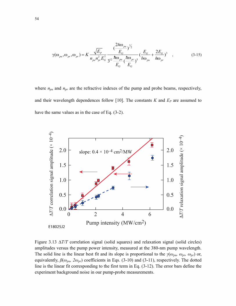
54
12
32 7
12 5
2( )
2( , , ) ( )3 ( )
pu
P G G Gpu pr pr
pu prpu pr G pu pr
G G
E E E EKn n E
E E
, (3-15)
where npu and npr are the refractive indexes of the pump and probe beams, respectively,
and their wavelength dependences follow [10]. The constants K and EP are assumed to
have the same values as in the case of Eq. (3-2).
Figure 3.13 ∆T/T correlation signal (solid squares) and relaxation signal (solid circles) amplitudes versus the pump power intensity, measured at the 380-nm pump wavelength. The solid line is the linear best fit and its slope is proportional to the γ(ωpu, ωpr, ωpr) or, equivalently, β(ωpu, 2ωpr) coefficients in Eqs. (3-10) and (3-11), respectively. The dotted line is the linear fit corresponding to the first term in Eq. (3-12). The error bars define the experiment background noise in our pump-probe measurements.
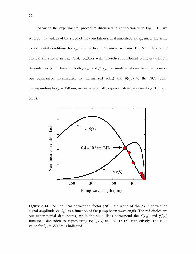
55
Following the experimental procedure discussed in connection with Fig. 3.13, we
recorded the values of the slope of the correlation signal amplitude vs. Ipu under the same
experimental conditions for λpu ranging from 360 nm to 430 nm. The NCF data (solid
circles) are shown in Fig. 3.14, together with theoretical functional pump-wavelength
dependences (solid lines) of both γ(λpu) and β (λpu), as modeled above. In order to make
our comparison meaningful, we normalized γ(λpu) and β(λpu) to the NCF point
corresponding to λpu = 380 nm, our experimentally representative case (see Figs. 3.11 and
3.13).
Figure 3.14 The nonlinear correlation factor (NCF–the slope of the ∆T/T correlation signal amplitude vs. Ipu) as a function of the pump beam wavelength. The red circles are our experimental data points, while the solid lines correspond the β(λpu) and γ(λpu) functional dependences, representing Eq. (3-3) and Eq. (3-15), respectively. The NCF value for λpu = 380 nm is indicated.
250 300 350 400
(l)
Non
linea
r cor
rela
tion
fact
or
Pump wavelength (nm)
(l)
0.4 × 10⁻⁴ cm2/MW
56
We clearly see in Fig. 3.14 that, within the pump wavelength range achievable by our
experimental setup, our NCF data points are only in a very good agreement with the β(λ)
functional dependence [Eq. (3-3)]. The latter indicates that, in our experimental case, the
TPA process is actually responsible for the nonlinear correlation signal. Unfortunately, we
were unable to directly measure the SHG process for the probe beam in our AlGaN
samples (we could only see a very faint indigo scattered light, when our crystal was
illuminated by the probe beam).
Examination of our experimental data showed that two different processes
contributed to the probe-beam ∆T/T transients measured in our experiments. The first was
the 310-fs-wide correlation signal, observed near the zero-delay point, and corresponded
to the TPA correlation process involving a simultaneous absorption of one UV pump
photon and one SHG photon from the probe beam. The correlation peak was followed by
a much slower (tens of picosecond in duration) transient representing relaxation of
photo-excited carriers in AlGaN and characterized by the bi-exponential photoresponse
decay. The amplitudes of both the correlation and relaxation signals dependences on the
pump power intensity (with the probe beam intensity constant) followed modeling based
on a generalized nondegenerate TPA process described in Ref. 6. Our analysis of the ∆T/T
correlation peak amplitude on the pump wavelength allowed us to demonstrate that its
spectral dependence, within our laser tuning range, agreed very well with the
Sheik-Bahae and Hutchings theory for the TPA coefficient. This indicates that the TPA
process, consisting of one pump and one SHG probe photons, dominated in our nonlinear
57
experiment.
3.4. Coherent acoustic phonon dynamics in GaN single crystals
Acoustic phonon oscillations in solids have most recently been investigated with a great
interest, not only from the fundamental physics point of view, but also for their potential
applications in photo-acoustic microscopy of nanostructures, THz acoustic-optic
modulation, coherent sources for phonon spectroscopy, and, finally, nanoscale acoustic
imaging [12-16]. In semiconductors, absorption of an ultrashort optical pulse generates
picosecond in duration acoustic transients (coherent-phonon bursts) due to a variety of
mechanisms, such as electric and/or thermal stress, deformation potential coupling, or the
piezoelectric effect. Propagating phonons cause a periodic modulation of the optical
properties of the semiconductor, which is usually detected by changes in reflectivity of
delayed optical probe pulses. CAPs in GaN films were first observed by Huang et al. [13]
and, subsequently, were thoroughly investigated by Wu et al. [17-21] in bulk GaN
crystals. Following research of Wu, using fixed (long) optical delays between the pump
and probe beams, we have, subsequently, demonstrated [19,20] that CAPs in GaN bulk
samples can propagate macroscopic distances without losing their coherence in room
temperature. We have also reported on strong CAP transients in ultra-thin GaN single
crystals and on the intrinsic CAP lifetime with a modified experimental geometry. [22]
58
3.4.1 Generation of CAPS in GaN single crystals
The all-optical CAP generation and detection mechanisms in bulk GaN crystals were
investigated in detail by Wu et al. [18], based on the seminal work of Thomsen et al. [12].
The approach to the CAP generation reduces to a one-dimensional (1-D) problem, based
on the 1-D elastic wave equation:
),(),(),(2
22
2
2
tzSzz
tzvt
tz zzs
zz
(3-16)
The driving force S(z,t) is related to the both electronic and thermal stress [18,20]. Figure
3.15 presents an example of numerically computed profiles of CAP transients, generated
by the electronic stress, thermal stress, and the sum of both, respectively. The CAP wave
packets were calculated in this case for the far-above-bandgap pump-photon excitation.
We note that the CAP pulses have strength of the order of 10-5 and a spatial width of
approximately twice the pump beam penetration depth.
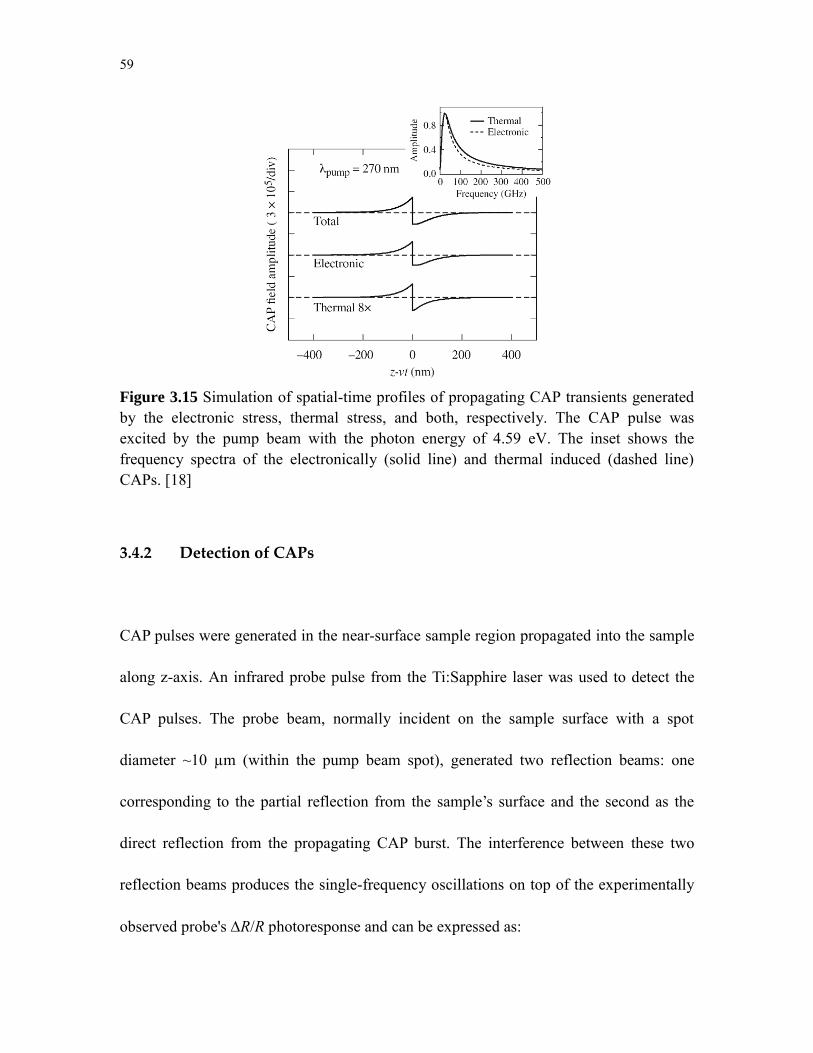
59
Figure 3.15 Simulation of spatial-time profiles of propagating CAP transients generated by the electronic stress, thermal stress, and both, respectively. The CAP pulse was excited by the pump beam with the photon energy of 4.59 eV. The inset shows the frequency spectra of the electronically (solid line) and thermal induced (dashed line) CAPs. [18]
3.4.2 Detection of CAPs
CAP pulses were generated in the near-surface sample region propagated into the sample
along z-axis. An infrared probe pulse from the Ti:Sapphire laser was used to detect the
CAP pulses. The probe beam, normally incident on the sample surface with a spot
diameter ~10 µm (within the pump beam spot), generated two reflection beams: one
corresponding to the partial reflection from the sample’s surface and the second as the
direct reflection from the propagating CAP burst. The interference between these two
reflection beams produces the single-frequency oscillations on top of the experimentally
observed probe's R/R photoresponse and can be expressed as:
60
dtftARR /-e)2sin(
, (3-17)
where the amplitude A and the phase φ are the only pump-beam-energy dependent
parameters and f is the frequency CAP oscillations. Since f comes from the self-inference
of the probe light, reflected from the sample at near normal incidence, it is given by
2probe
probe
n nf k
, (3-18)
where v is the speed of sound in GaN and kprobe = 2π/probe is the probe-light wave vector.
Finally, τd is the experimental decay time and can be expressed as
1 1prb
d phonon
, (3-19)
where τphonon is the CAP intrinsic decay time, and αprb is the probe light absorption
coefficient.
3.4.3 Propagation of CAPs in GaN
Figure 3.16(a) shows the time-resolved ΔR/R transient, obtained using our one-color
pump-probe setup operating at 355 nm. We note the CAP oscillations, which are
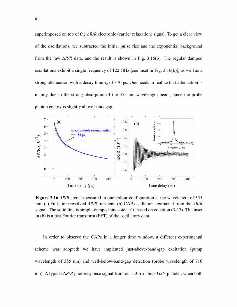
61
superimposed on top of the ΔR/R electronic (carrier relaxation) signal. To get a clear view
of the oscillations, we subtracted the initial pulse rise and the exponential background
from the raw ΔR/R data, and the result is shown in Fig. 3.16(b). The regular damped
oscillations exhibit a single frequency of 122 GHz [see inset in Fig. 3.16(b)], as well as a
strong attenuation with a decay time τd of ~70 ps. One needs to realize that attenuation is
mainly due to the strong absorption of the 355 nm wavelength beam, since the probe
photon energy is slightly above bandagap.
Figure 3.16 ΔR/R signal measured in one-colour configuration at the wavelength of 355 nm. (a) Full, time-resolved ΔR/R transient. (b) CAP oscillations extracted from the ΔR/R signal. The solid line is simple-damped sinusoidal fit, based on equation (3-17). The inset in (b) is a fast Fourier transform (FFT) of the oscillatory data.
In order to observe the CAPs in a longer time window, a different experimental
scheme was adopted: we have implented just-above-band-gap excitation (pump
wavelength of 355 nm) and well-below-band-gap detection (probe wavelength of 710
nm). A typical R/R photoresponse signal from our 50-µm -thick GaN platelet, when both
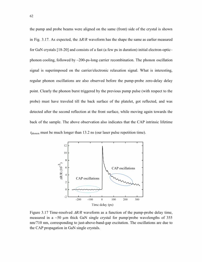
62
the pump and probe beams were aligned on the same (front) side of the crystal is shown
in Fig. 3.17. As expected, the R/R waveform has the shape the same as earlier measured
for GaN crystals [18-20] and consists of a fast (a few ps in duration) initial electron-optic–
phonon cooling, followed by ~200-ps-long carrier recombination. The phonon oscillation
signal is superimposed on the carrier/electronic relaxation signal. What is interesting,
regular phonon oscillations are also observed before the pump-probe zero-delay delay
point. Clearly the phonon burst triggered by the previous pump pulse (with respect to the
probe) must have traveled till the back surface of the platelet, got reflected, and was
detected after the second reflection at the front surface, while moving again towards the
back of the sample. The above observation also indicates that the CAP intrinsic lifetime
phonon must be much longer than 13.2 ns (our laser pulse repetition time).
Figure 3.17 Time-resolved R/R waveform as a function of the pump-probe delay time, measured in a ~50 m thick GaN single crystal for pump/probe wavelengths of 355 nm/710 nm, corresponding to just-above-band-gap excitation. The oscillations are due to the CAP propagation in GaN single crystals.
CAP oscillations
CAP oscillations
63
3.4.4 CAP lifetime measurement
Following Refs 19 and 21, we have demonstrated that the ultra-long-lived CAPs have an
intrinsic lifetime phonon of at least 70 ns at room temperature, by investigating the CAP
oscillations at longer time windows, using fixed optical delays between the pump and
probe. The actual phonon value is likely to be longer, since our ~100 fs probe pulses not
only attenuate, but also disperse as they propagate inside the GaN, what would be another
contribution to d [21].
In order to eliminate dispersion of probe pulses, we have developed a modified
experimental geometry. The method for optical generation and time-resolved detection of
CAPs is shown schematically in Fig. 3.18. Both one- and two-sides pump-probe
spectroscopy experiments were performed on bulk GaN single crystals in the reflection
mode. Details of the testing setup working principle have been presented in the
pump-probe spectroscopy part in Chapter 2. Since in our modified experimental scheme,
the probe beam does not penetrate deep inside the sample crystal, the second term of Eq.
(3-19) can be neglected. This two-surfaces measurement geometry allows us to directly
determine the CAPs’ lifetime, by the simplified form of Eq. (3-19):
d phonon . (3-20)
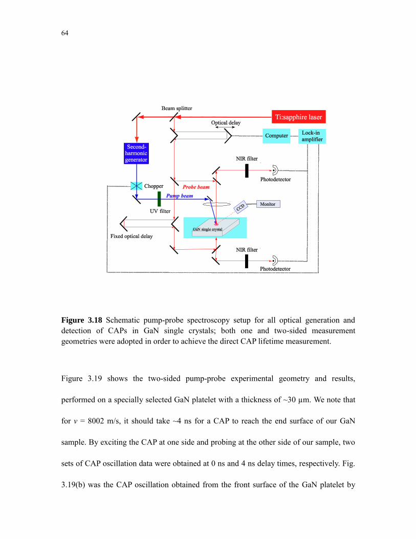
64
Figure 3.18 Schematic pump-probe spectroscopy setup for all optical generation and detection of CAPs in GaN single crystals; both one and two-sided measurement geometries were adopted in order to achieve the direct CAP lifetime measurement.
Figure 3.19 shows the two-sided pump-probe experimental geometry and results,
performed on a specially selected GaN platelet with a thickness of ~30 µm. We note that
for v = 8002 m/s, it should take ~4 ns for a CAP to reach the end surface of our GaN
sample. By exciting the CAP at one side and probing at the other side of our sample, two
sets of CAP oscillation data were obtained at 0 ns and 4 ns delay times, respectively. Fig.
3.19(b) was the CAP oscillation obtained from the front surface of the GaN platelet by
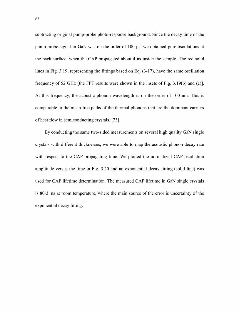
65
subtracting original pump-probe photo-response background. Since the decay time of the
pump-probe signal in GaN was on the order of 100 ps, we obtained pure oscillations at
the back surface, when the CAP propagated about 4 ns inside the sample. The red solid
lines in Fig. 3.19, representing the fittings based on Eq. (3-17), have the same oscillation
frequency of 52 GHz [the FFT results were shown in the insets of Fig. 3.19(b) and (c)].
At this frequency, the acoustic phonon wavelength is on the order of 100 nm. This is
comparable to the mean free paths of the thermal phonons that are the dominant carriers
of heat flow in semiconducting crystals. [23]
By conducting the same two-sided measurements on several high quality GaN single
crystals with different thicknesses, we were able to map the acoustic phonon decay rate
with respect to the CAP propagating time. We plotted the normalized CAP oscillation
amplitude versus the time in Fig. 3.20 and an exponential decay fitting (solid line) was
used for CAP lifetime determination. The measured CAP lifetime in GaN single crystals
is 80±3 ns at room temperature, where the main source of the error is uncertainty of the
exponential decay fitting.
66
Figure 3.19 (a) Two-sided experimental geometry for direct measurement of the CAP lifetime. (b) CAP oscillations obtained at the front surface of the GaN single crystal right after the generation of acoustic phonons. (c) CAP oscillations obtained on the back surface of the GaN sample, after CAP has propagated a distance of the sample’s thickness (~ 4 ns). The solid red lines on the experimental data are the best fitting of the oscillations using Eq. (3-17). The insets of the (b) and (c) show the Fourier transform of the two data sets and have the same peak frequency of 52 GHz.
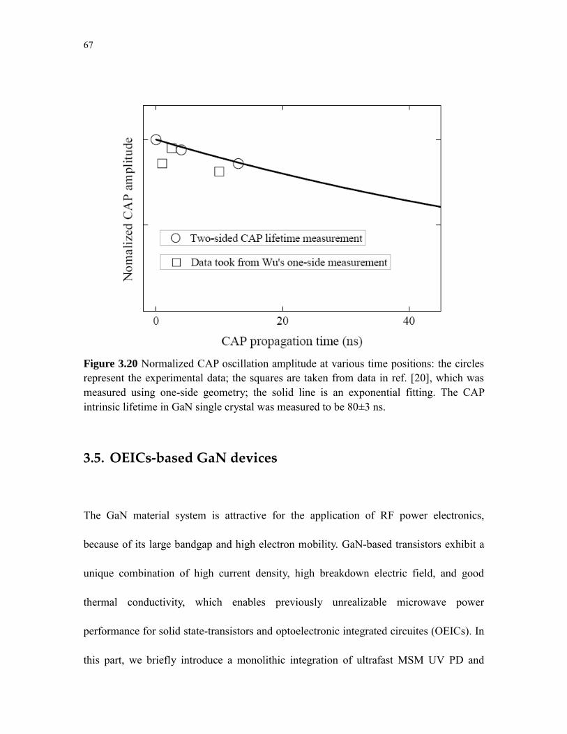
67
Figure 3.20 Normalized CAP oscillation amplitude at various time positions: the circles represent the experimental data; the squares are taken from data in ref. [20], which was measured using one-side geometry; the solid line is an exponential fitting. The CAP intrinsic lifetime in GaN single crystal was measured to be 80±3 ns.
3.5. OEICs-based GaN devices
The GaN material system is attractive for the application of RF power electronics,
because of its large bandgap and high electron mobility. GaN-based transistors exhibit a
unique combination of high current density, high breakdown electric field, and good
thermal conductivity, which enables previously unrealizable microwave power
performance for solid state-transistors and optoelectronic integrated circuites (OEICs). In
this part, we briefly introduce a monolithic integration of ultrafast MSM UV PD and
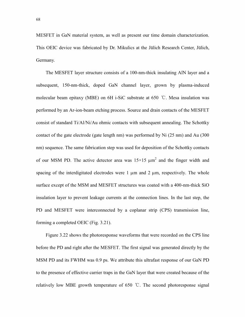
68
MESFET in GaN material system, as well as present our time domain characterization.
This OEIC device was fabricated by Dr. Mikulics at the Jülich Research Center, Jülich,
Germany.
The MESFET layer structure consists of a 100-nm-thick insulating AlN layer and a
subsequent, 150-nm-thick, doped GaN channel layer, grown by plasma-induced
molecular beam epitaxy (MBE) on 6H i-SiC substrate at 650 ℃. Mesa insulation was
performed by an Ar-ion-beam etching process. Source and drain contacts of the MESFET
consist of standard Ti/Al/Ni/Au ohmic contacts with subsequent annealing. The Schottky
contact of the gate electrode (gate length nm) was performed by Ni (25 nm) and Au (300
nm) sequence. The same fabrication step was used for deposition of the Schottky contacts
of our MSM PD. The active detector area was 15×15 m2 and the finger width and
spacing of the interdigitated electrodes were 1 m and 2 m, respectively. The whole
surface except of the MSM and MESFET structures was coated with a 400-nm-thick SiO
insulation layer to prevent leakage currents at the connection lines. In the last step, the
PD and MESFET were interconnected by a coplanar strip (CPS) transmission line,
forming a completed OEIC (Fig. 3.21).
Figure 3.22 shows the photoresponse waveforms that were recorded on the CPS line
before the PD and right after the MESFET. The first signal was generated directly by the
MSM PD and its FWHM was 0.9 ps. We attribute this ultrafast response of our GaN PD
to the presence of effective carrier traps in the GaN layer that were created because of the
relatively low MBE growth temperature of 650 ℃. The second photoresponse signal
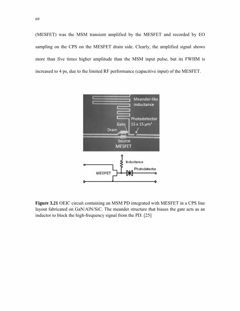
69
(MESFET) was the MSM transient amplified by the MESFET and recorded by EO
sampling on the CPS on the MESFET drain side. Clearly, the amplified signal shows
more than five times higher amplitude than the MSM input pulse, but its FWHM is
increased to 4 ps, due to the limited RF performance (capacitive input) of the MESFET.
Figure 3.21 OEIC circuit containing an MSM PD integrated with MESFET in a CPS line layout fabricated on GaN/AlN/SiC. The meander structure that biases the gate acts as an inductor to block the high-frequency signal from the PD. [25]
70
Figure 3.22 OEIC circuit containing an MSM PD integrated with MESFET in a CPS line layout fabricated on GaN/AlN/SiC. The meander structure that biases the gate acts as an inductor to block the high-frequency signal from the PD.
3.6. Summary
This Chapter is focused on the phonon and carrier dynamics in III-Nitrides, such as,
GaN and AlGaN single crystals. Both sets of approximately 12 samples were provided by
Prof. Karpinski’s High Pressure Material Synthesis Group in ETH, Zurich. We performed
all-optical generation and detection of CAPs in GaN single crystals. In addition, to
accurately determine the phonon lifetime, we designed the two-side measurements and
observed the phonon decay with respect to its propagation time. The phonon lifetime is
~80 ns in GaN single crystals.
We also investigated the NLO properties of AlGaN single crystals using a
two-color/two-beam modified femtosecond pump-probe technique. By scanning in time
71
domain the probe ΔT/T signal, we observed a 310-fs-wide, Gaussian-shaped correlation
signal. Our analysis of the ∆T/T correlation peak amplitude on the pump wavelength
allowed us to demonstrate that its spectral dependence agreed very well with the
Sheik-Bahae and Hutchings theory for the TPA coefficient. The latter indicates that the
TPA process, consisting of one pump and one SHG probe photons, dominated in our
nonlinear experiment.
Finally, we investigated the performance of an integrated optoelectronic circuit,
consisting of a MSM PD and a MESFET, both fabricated in the same GaN chip system.
The PD shows pulse response with sub-ps FWHM and a corresponding bandwidth of 410
GHz. At low frequencies, the MESFET amplified amplitude shows an about tenfold
amplitude, compared to the MSM signal. The 3-dB bandwidth of the MESFET is 55
GHz.
72
Bibliography
[1] J. Karpinski, J. Jun and S. Porowski, J. Cryst. Growth 66, 1 (1984).
[2] A. Belousov, S. Katrych, J. Jun, J. Karpinski, B. Batlogg, D. Günther, J. Zhang, and
R. Sobolewski, J. Cryst. Growth 311, 3971- (2009).
[3] Ilker Ay, Huseyin, Turk. J. Phys., 25 215 (2001).
[4] B. Batlogg and P. Watcher, Solid State Communications, 24, 569, (1977).
[5] S. Krishnamurthy, K. Nashold, and A. Sher, Appl. Phys. Lett. 77, 355 (2000).
[6] C. Rauscher and R. Laenen, J. Appl. Phys., 81(6), 2818 (1997).
[7] M. Sheik-Bahae, D. C. Hutchings, D. J. Hagan, and E. W. Van Stryland, IEEE J.
Quantum Electron. 27, 1296 (1991).
[8] D. C. Hutchings and E. W Van Stryland, J. Opt. Soc. Am. B, 9, 11 (1992).
[9] A. Othonos, J. Appl. Phys. 83, 1789 (1998).
[10] M. Stutzmann, O. Ambacher, A. Cros, M. S. Brandt, H. Angerer, R. Dimitrov, N.
Reinacher, T. Metzger, R. Höpler, D. Brunner, F. Freudenberg, R. Handschuh, and
Ch. Deger, Mater. Sci. Eng. B 50, 212 (1997).
[11] B. S. Wherrett, J. Opt. Soc. Am. B 1, 67 (1984).
[12] C. Thomsen, H. T. Grahn, H. J. Maris, and J. Tauc, Phys. Rev. B 34, 4129, (1986).
[13] Y. K. Huang, G. W. Chen, and C. K. Sun, Appl. Phys. Lett. 79, 3361, (2001).
73
[14] O. Matsuda, O. B. Wright, D. H. Hurley, V. E. Cusev, and K. Shimizu, Phys. Rev.
Lett. 93, 095501, (2004).
[15] C. K. Sun, J. C. Liang, and X. Y. Yu, Phys. Rev. Lett. 84, 179, (2000).
[16] B. C. Daly, N. C. R. Holme, T. Buma, et al. Appl. Phys. Lett. 84, 5180, (2004).
[17] S. Wu, P. Geiser, J. Jun, J. Karpinski, J. R. Park and R. Sobolewski, Appl. Phys. Lett.
88, 041917, (2006).
[18] S. Wu, P. Geiser, J. Jun, J. Karpinski, and R. Sobolewski, Phys. Rev. B 76, 085210,
(2007).
[19] S. Wu, J. Zhang, A. Belousov, J. Karpinski, and R. Sobolewski in Gallium Nitride
Materials and Devices III, ed. by H. Morkoç, C. W. Litton, J.-I. Chyi, Y. Nanishi, and
E. Yoon, Proc. of SPIE, 6894, 68940K, (2008).
[20] S. Wu, “Time-resloved characterization of carrier and phonon dynamics in GaN
single crystals”, PhD thesis, University of Rochester, (2007).
[21] S. Wu, J. Zhang, A. Belousov, J. karpinski, and R. Sobolewski, J. Physcis
Conference Series 92, 012021, (2007).
[22] J. Zhang, A. Belousov, J. karpinski, and R. Sobolewski, “Direct measurement of the
intrinsic lifetime of coherent acoustic phonon in GaN single crystals”, Appl. Phys.
Lett. in print.
[23] B. A. Danilchenko, T. Paszkiewicz, S. Wolski, A. Jeowski, and T. Plackowski, Appl.
Phys. Lett. 89. 061901 (2006).
[24] H. N. Lin, R. J. Stoner, H. J. Maris, and J. Tauc, J. Appl. Phys. 69(7), 3816, (1991).

74
[25] M. Mikulics, P. Kordoš, D. Gregušová, R. Adam, M. Kočan, S. Wu, J. Zhang, R.
Sobolewski, D. Grützmacher, and M. Marso, IEEE Phot. Tech. lett., 23, 17, (2011).
75
4. THz bandwidth photo-response of
free-standing GaAs meso-structures
Ultrahigh-speed photonic devices, such as ultrafast photo-switches, photo-mixers, and
PDs, based on III-V semiconducting compounds, have been studied intensively in recent
years, [1,2] with a special emphasis focused on the GaAs material, due to its excellent
electronic transport and optoelectronic properties. GaAs-based devices are commonly
used in high-end commercial applications, such as satellite communication systems and
radars. [3] A special material called low-temperature–grown GaAs (LT-GaAs), since it
exhibits <200 fs carrier lifetime, has been very successfully implemented in the fastest
PDs [4,5] and THz photo-mixers [6]. Independently, during the last decade, there has
been an explosive growth of interest in novel nanodevices, based on low-dimensional,
nanometer-sized structures. One of the most popular devices is the single-crystal
semiconducting nanowhiskers and/or nanowires that have demonstrated a unique
potential in photonics applications. [7-10] In this chapter, we will report our investigation
on epitaxially grown free-standing, single-crystal GaAs meso-structures.
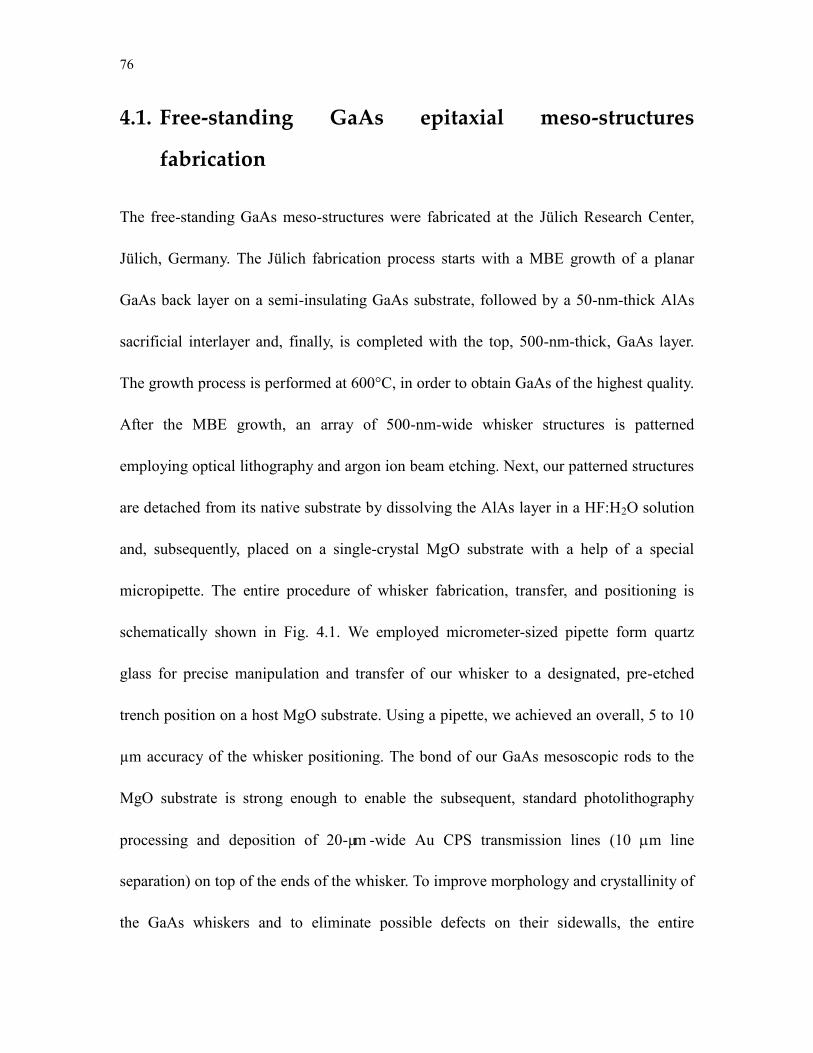
76
4.1. Free-standing GaAs epitaxial meso-structures
fabrication
The free-standing GaAs meso-structures were fabricated at the Jülich Research Center,
Jülich, Germany. The Jülich fabrication process starts with a MBE growth of a planar
GaAs back layer on a semi-insulating GaAs substrate, followed by a 50-nm-thick AlAs
sacrificial interlayer and, finally, is completed with the top, 500-nm-thick, GaAs layer.
The growth process is performed at 600°C, in order to obtain GaAs of the highest quality.
After the MBE growth, an array of 500-nm-wide whisker structures is patterned
employing optical lithography and argon ion beam etching. Next, our patterned structures
are detached from its native substrate by dissolving the AlAs layer in a HF:H2O solution
and, subsequently, placed on a single-crystal MgO substrate with a help of a special
micropipette. The entire procedure of whisker fabrication, transfer, and positioning is
schematically shown in Fig. 4.1. We employed micrometer-sized pipette form quartz
glass for precise manipulation and transfer of our whisker to a designated, pre-etched
trench position on a host MgO substrate. Using a pipette, we achieved an overall, 5 to 10
µm accuracy of the whisker positioning. The bond of our GaAs mesoscopic rods to the
MgO substrate is strong enough to enable the subsequent, standard photolithography
processing and deposition of 20-µm -wide Au CPS transmission lines (10 m line
separation) on top of the ends of the whisker. To improve morphology and crystallinity of
the GaAs whiskers and to eliminate possible defects on their sidewalls, the entire
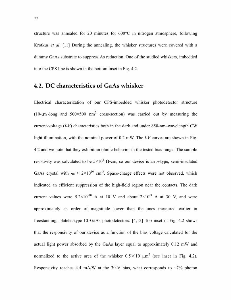
77
structure was annealed for 20 minutes for 600°C in nitrogen atmosphere, following
Krotkus et al. [11] During the annealing, the whisker structures were covered with a
dummy GaAs substrate to suppress As reduction. One of the studied whiskers, imbedded
into the CPS line is shown in the bottom inset in Fig. 4.2.
4.2. DC characteristics of GaAs whisker
Electrical characterization of our CPS-imbedded whisker photodetector structure
(10-µm -long and 500×500 nm2 cross-section) was carried out by measuring the
current-voltage (I-V) characteristics both in the dark and under 850-nm–wavelength CW
light illumination, with the nominal power of 0.2 mW. The I-V curves are shown in Fig.
4.2 and we note that they exhibit an ohmic behavior in the tested bias range. The sample
resistivity was calculated to be 5×10⁴ Ω•cm, so our device is an n-type, semi-insulated
GaAs crystal with n0 ≈ 2×1010 cm-3. Space-charge effects were not observed, which
indicated an efficient suppression of the high-field region near the contacts. The dark
current values were 5.2×10⁻¹⁰ A at 10 V and about 2×10⁻⁹ A at 30 V, and were
approximately an order of magnitude lower than the ones measured earlier in
freestanding, platelet-type LT-GaAs photodetectors. [4,12] Top inset in Fig. 4.2 shows
that the responsivity of our device as a function of the bias voltage calculated for the
actual light power absorbed by the GaAs layer equal to approximately 0.12 mW and
normalized to the active area of the whisker 0.5×10 m2 (see inset in Fig. 4.2).
Responsivity reaches 4.4 mA/W at the 30-V bias, what corresponds to ~7% photon
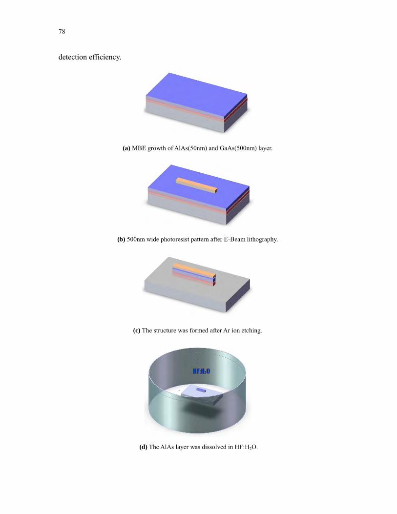
78
detection efficiency.
(a) MBE growth of AlAs(50nm) and GaAs(500nm) layer.
(b) 500nm wide photoresist pattern after E-Beam lithography.
(c) The structure was formed after Ar ion etching.
(d) The AlAs layer was dissolved in HF:H2O.
79
(e) After rising in deionized water, the nanowhisker (NW) structure was
transferred with micropipeta.
(f) The NW structure was transferred to host substrate, into the
pre-etched trench.
(g) CPS lines was fabricated on top of the NW structure
Figure 4.1 Schematics of the epitaxial GaAs nanowhikser fabrication process.
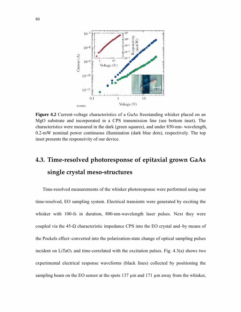
80
Figure 4.2 Current-voltage characteristics of a GaAs freestanding whisker placed on an MgO substrate and incorporated in a CPS transmission line (see bottom inset). The characteristics were measured in the dark (green squares), and under 850-nm- wavelength, 0.2-mW nominal power continuous illumination (dark blue dots), respectively. The top inset presents the responsivity of our device.
4.3. Time-resolved photoresponse of epitaxial grown GaAs
single crystal meso-structures
Time-resolved measurements of the whisker photoresponse were performed using our
time-resolved, EO sampling system. Electrical transients were generated by exciting the
whisker with 100-fs in duration, 800-nm-wavelength laser pulses. Next they were
coupled via the 45-Ω characteristic impedance CPS into the EO crystal and–by means of
the Pockels effect–converted into the polarization-state change of optical sampling pulses
incident on LiTaO3 and time-correlated with the excitation pulses. Fig. 4.3(a) shows two
experimental electrical response waveforms (black lines) collected by positioning the
sampling beam on the EO sensor at the spots 137 µm and 171 µm away from the whisker,
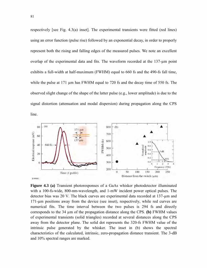
81
respectively [see Fig. 4.3(a) inset]. The experimental transients were fitted (red lines)
using an error function (pulse rise) followed by an exponential decay, in order to properly
represent both the rising and falling edges of the measured pulses. We note an excellent
overlap of the experimental data and fits. The waveform recorded at the 137-µm point
exhibits a full-width at half-maximum (FWHM) equal to 660 fs and the 490-fs fall time,
while the pulse at 171 µm has FWHM equal to 720 fs and the decay time of 550 fs. The
observed slight change of the shape of the latter pulse (e.g., lower amplitude) is due to the
signal distortion (attenuation and modal dispersion) during propagation along the CPS
line.
Figure 4.3 (a) Transient photoresponses of a GaAs whisker photodetector illuminated with a 100-fs-wide, 800-nm-wavelength, and 1-mW incident power optical pulses. The detector bias was 20 V. The black curves are experimental data recorded at 137-µm and 171-µm positions away from the device (see inset), respectively, while red curves are numerical fits. The time interval between the two pulses is 294 fs and directly corresponds to the 34 µm of the propagation distance along the CPS. (b) FWHM values of experimental transients (solid triangles) recorded at several distances along the CPS away from the detector plane. The solid dot represents the 320-fs FWHM value of the intrinsic pulse generated by the whisker. The inset in (b) shows the spectral characteristics of the calculated, intrinsic, zero-propagation distance transient. The 3-dB and 10% spectral ranges are marked.
82
We have collected several photoresponse transients along the CPS, starting with the
distance ~100 µm away of the whisker, and their values of FWHM (triangles) are plotted
in Fig. 4.3(b). Next, we performed the standard frequency-domain analysis [13] of our
signals in order to, first, determine the amount of distortion introduced by our CPS line
and, subsequently, calculate the actual, intrinsic transient generated by the photodetector,
by “back-propagating” an experimental transient, e.g., the one measured at 137 µm,
towards its zero distance plane (whisker position) on the CPS line. It is well known that,
an input voltage pulse V(0, t) be excited at the position z = 0 can be retrieved by the
technique of Fourier transformation of the propagated pulse V(z, t) at z:
1 ( )(0, ) { [ ( , )]}f zV t e V z t , (4-1)
Using the Fourier transform approach, temporal shape of a voltage pulse V(z,t) at the
position z can be retrieved from the known V(z1,t) transient measured at a different point
z1 along the line, if one knows the spectral characteristics of the complex propagation
factor γ(f) of the transmission line. The γ(f) factor can, in turn, be computed numerically
by comparing frequency spectra (taking their ratio) of two (or more for better accuracy)
experimental waveforms, measured at different positions along the transmission line.
Using the above approach, we have calculated the γ(f) spectral dependence for our CPS
line based on the experimental transients recorded at the positions along the CPS
indicated in Fig. 4.3(a). The γ(f) factor, however, can be written as (f) = (f) + j(f),
83
which includes the attenuation consant and phase constant . These two propagation
constants are frequency-dependent and can be computed, numerically, from the
experimental data at multiple positions. The attenuation and phase factors f) and f
are shown in Fig. 4.4. It is seen that f) has a quadratic dependence on f and f is
linearly increasing along with the frequency. We can also calculate the phase velocity of
the transient THz wave, using:
( ) 2 / ( )ph f f f . (4-2)
The signal phase velocity along the CPS lines is 1.16×10⁸ m/s and it agrees very well
with the velocity value computed using v = z/t for the two pulses data in Fig. 4.3(a).
Using our γ(f) factor and the Fourier transform of the signal collected at 137-µm
point [see Fig. 4.3(a)], we reproduced the temporal shape of the signal generated at the
whisker plane [V(z = 0,t)]. The resulting, intrinsic signal generated by our photodetector
had a peak amplitude Vs = 185.7 mV, FWHM = 320 fs, and a fall time of ~150 fs. The
rising edge was limited by the 100-fs width of our optical excitation pulse. The 320-fs
response time of our device is at least one order of magnitude faster than any
demonstrated nanostructures. [14] The FWHM value of V(0,t) is marked in Fig. 4.3(b) as
a solid dot, while the inset in Fig. 4.3(b) presents its spectral characteristics. We note that
our intrinsic photoresponse signal has a 3-dB bandwidth up to 1.3 THz and 10%
bandwidth of above 2.4 THz, making our GaAs single-crystal whisker a truly THz
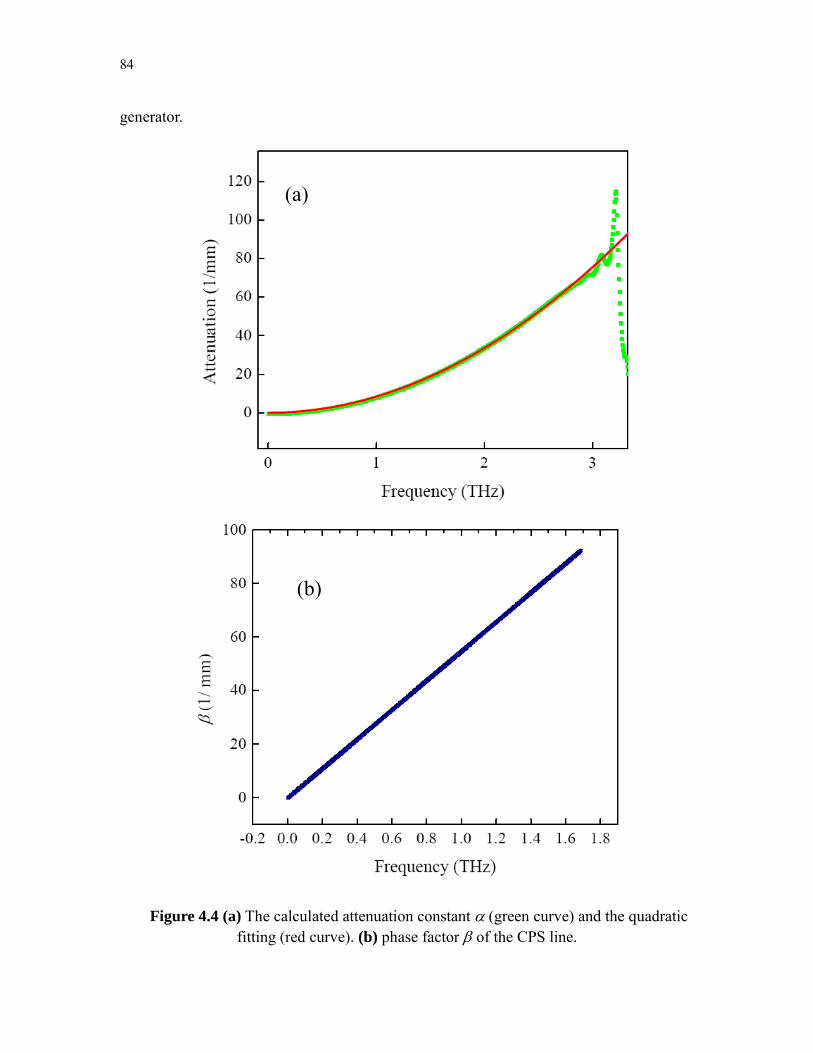
84
generator.
Figure 4.4 (a) The calculated attenuation constant (green curve) and the quadratic fitting (red curve). (b) phase factor of the CPS line.
(a)
(b)
85
We have also performed studies of the 500-nm-thick and 10×10 µm2 active area,
platelet PDs (see inset of Fig. 4.5) in order to determine if the performance of our whisker
was geometry limited, or, rather resulted from the intrinsic properties of the 500-nm-thick
epitaxial GaAs film. In both whisker and platelet cases, we measured the photoresponse
pulse FWHM and Vs dependences on the applied dc bias and the incident optical power.
The results were qualitatively identical, in the tested, 0–30 V, low-bias range (equipment
limited). Under the fixed (low) optical excitation power, the photoresponse FWHM
remained constant, while Vs increased linearly with the bias. The FWHM also remained
constant over the tested range of the incident optical power, while Vs initially increased
linearly and started to saturate when the incident power exceeded 3 mW. The most
striking, however, was that the photoresponse transients of platelet devices, measured
under the same conditions as whiskers (e.g., the same sampling spot distance), exhibited
practically the same, ~670 fs values of the FWHM, clearly indicating that in both types of
devices we observe the same bulk-material carrier relaxation dynamics and not, e.g.,
geometry- and/or surface-related electron trapping effects.
To further investigate the intrinsic material photo-response, we also performed two
types of pump-probe spectroscopy studies on the GaAs platelet. Figure 4.5 shows both
the one-color (800 nm/800 nm) and two-color (400 nm/800 nm) pump-probe
photoresponse signals, solid and dot-dashed lines, respectively. For 800-nm excitation,
the signal has a FWHM of 310 fs and fall time of 290 fs, which again confirms that, both
whisker and platelet structures have the same intrinsic response at 800 nm illumination.
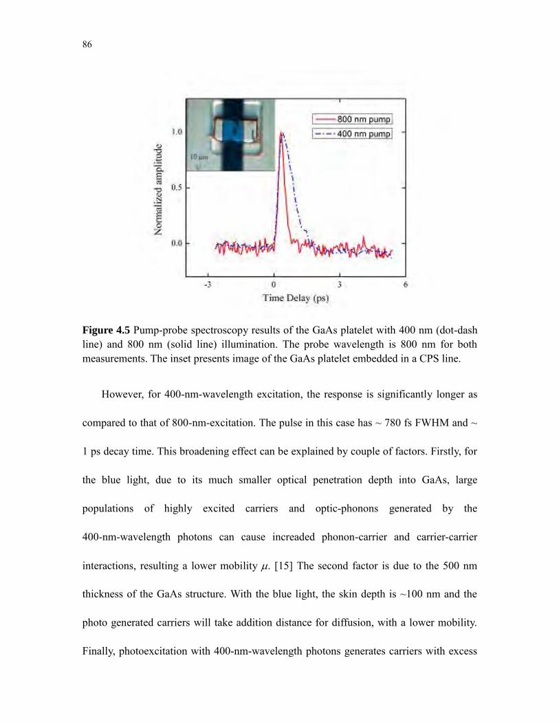
86
Figure 4.5 Pump-probe spectroscopy results of the GaAs platelet with 400 nm (dot-dash line) and 800 nm (solid line) illumination. The probe wavelength is 800 nm for both measurements. The inset presents image of the GaAs platelet embedded in a CPS line.
However, for 400-nm-wavelength excitation, the response is significantly longer as
compared to that of 800-nm-excitation. The pulse in this case has ~ 780 fs FWHM and ~
1 ps decay time. This broadening effect can be explained by couple of factors. Firstly, for
the blue light, due to its much smaller optical penetration depth into GaAs, large
populations of highly excited carriers and optic-phonons generated by the
400-nm-wavelength photons can cause increaded phonon-carrier and carrier-carrier
interactions, resulting a lower mobility . [15] The second factor is due to the 500 nm
thickness of the GaAs structure. With the blue light, the skin depth is ~100 nm and the
photo generated carriers will take addition distance for diffusion, with a lower mobility.
Finally, photoexcitation with 400-nm-wavelength photons generates carriers with excess
87
energy of ~ 1.6 eV at 300 K. The excess energy initially results in high kinetic energy of
carriers and a high electron temperature. Since the L and X valley minima in GaAs are
only 0.29 and 0.48 eV above the valley minimum, respectively, these photo-induced
carriers have enough energy to undergo intervalley scattering. The intervalley scattering
occurs on the 10-100 fs time scale, via emission of large wave-vector phonons. [16] The
large wave-vector phonons must decay through multiphonon processes. Those carriers
staying within the upper valley also relax to the bottom of valley by emitting
phonons. However, before reaching equilibrium, carriers can emit or absorb “hot”
phonons and the carriers cannot relax until the “hot” phonon population relaxes, which
occurs with a time constant of 1-4 ps. [15] The ~ 1 ps decay time agrees well with the
above very hot carrier relaxation model.
The time-resolved EO studies also allowed us to determine carrier mobility in our
meso-structures. Following Ref. 17, we used the expression for the total charge
(integrated photocurrent) generated in our photodetector upon laser pulse excitation, and,
subsequently, compared it directly to the photoresponse signal (peak current equals Vs/45
Ω). For calculations [see, e.g., Eq. (1) in Ref. 4], we used our experimental parameters for
the optical excitation and sample geometry, as well as the responsivity value taken from
the inset in Fig. 4.2 at the actual 20-V bias. Thus, the only unknown parameter was the
sample mobility, which turned out to be ~7300 cm2/V•s. We note that this is a very
respectable (bulk like) value for our meso-sized structures and it clearly indicates that,
indeed, our devices are very high quality bars of the GaAs single crystal. The latter
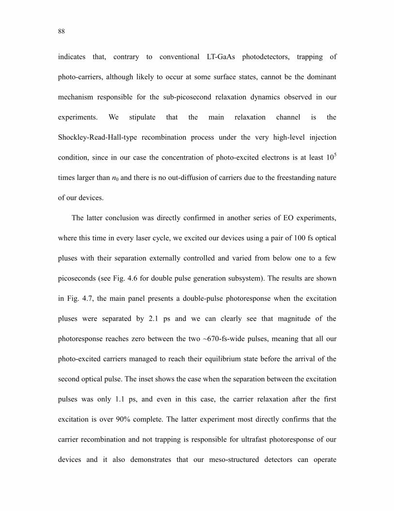
88
indicates that, contrary to conventional LT-GaAs photodetectors, trapping of
photo-carriers, although likely to occur at some surface states, cannot be the dominant
mechanism responsible for the sub-picosecond relaxation dynamics observed in our
experiments. We stipulate that the main relaxation channel is the
Shockley-Read-Hall-type recombination process under the very high-level injection
condition, since in our case the concentration of photo-excited electrons is at least 105
times larger than n0 and there is no out-diffusion of carriers due to the freestanding nature
of our devices.
The latter conclusion was directly confirmed in another series of EO experiments,
where this time in every laser cycle, we excited our devices using a pair of 100 fs optical
pluses with their separation externally controlled and varied from below one to a few
picoseconds (see Fig. 4.6 for double pulse generation subsystem). The results are shown
in Fig. 4.7, the main panel presents a double-pulse photoresponse when the excitation
pluses were separated by 2.1 ps and we can clearly see that magnitude of the
photoresponse reaches zero between the two ~670-fs-wide pulses, meaning that all our
photo-excited carriers managed to reach their equilibrium state before the arrival of the
second optical pulse. The inset shows the case when the separation between the excitation
pulses was only 1.1 ps, and even in this case, the carrier relaxation after the first
excitation is over 90% complete. The latter experiment most directly confirms that the
carrier recombination and not trapping is responsible for ultrafast photoresponse of our
devices and it also demonstrates that our meso-structured detectors can operate
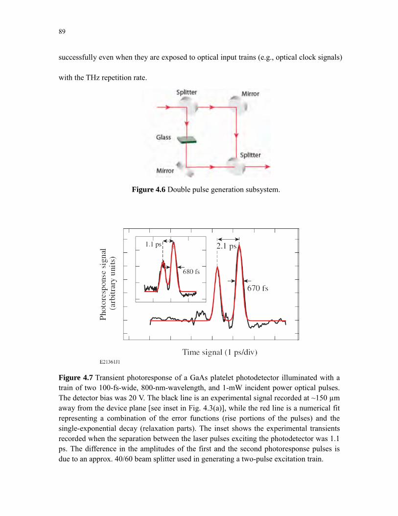
89
successfully even when they are exposed to optical input trains (e.g., optical clock signals)
with the THz repetition rate.
Figure 4.6 Double pulse generation subsystem.
Figure 4.7 Transient photoresponse of a GaAs platelet photodetector illuminated with a train of two 100-fs-wide, 800-nm-wavelength, and 1-mW incident power optical pulses. The detector bias was 20 V. The black line is an experimental signal recorded at ~150 µm away from the device plane [see inset in Fig. 4.3(a)], while the red line is a numerical fit representing a combination of the error functions (rise portions of the pulses) and the single-exponential decay (relaxation parts). The inset shows the experimental transients recorded when the separation between the laser pulses exciting the photodetector was 1.1 ps. The difference in the amplitudes of the first and the second photoresponse pulses is due to an approx. 40/60 beam splitter used in generating a two-pulse excitation train.
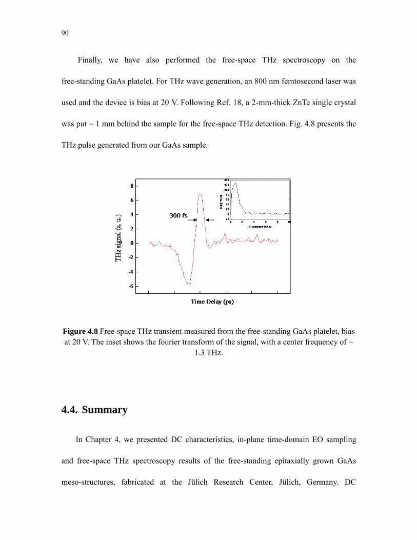
90
Finally, we have also performed the free-space THz spectroscopy on the
free-standing GaAs platelet. For THz wave generation, an 800 nm femtosecond laser was
used and the device is bias at 20 V. Following Ref. 18, a 2-mm-thick ZnTe single crystal
was put ~ 1 mm behind the sample for the free-space THz detection. Fig. 4.8 presents the
THz pulse generated from our GaAs sample.
Figure 4.8 Free-space THz transient measured from the free-standing GaAs platelet, bias at 20 V. The inset shows the fourier transform of the signal, with a center frequency of ~
1.3 THz.
4.4. Summary
In Chapter 4, we presented DC characteristics, in-plane time-domain EO sampling
and free-space THz spectroscopy results of the free-standing epitaxially grown GaAs
meso-structures, fabricated at the Jülich Research Center, Jülich, Germany. DC
91
characterization showed that our device has an extremely low dark current. Both FWMH
and signal amplitude as a function of bias voltage and incident power were investigated.
Frequency-domain analysis was also performed to obtain the pulse propagation properties
along CPS lines using multiple positioned pulses. The reproduction calculation retrieved
the genuine intrinsic response of the GaAs NW structure and showed that it has a
bandwidth of up to 1.3 THz. As a photodetector, the freestanding, epitaxial GaAs element
is truly unique, as it combines extremely low dark currents and ~7% single-photon
detection efficiency with a sub-picosecond photoresponse and assures successful
operation even in optical systems with THz laser clock-pulse rates.
92
Bibliography
[1] N. Dagli (Ed.). High-Speed Photonic Devices, CRC Press Series in Optics and
Optoelectronics, Taylor&Francis Group, Boca Raton, FL (2007), and references
therein.
[2] G. Steinmeyer, J. Opt. A: Pure Appl. Opt., 5, R1 (2003), and references therein.
[3] M. E. Kim, et al., IEEE Trans. Microwave Theory Tech., 37, 1286 (1989).
[4] Zheng, X. et al. Appl. Opt. 42, 1726 (2003).
[5] M. Mikulics, et al. IEEE Phot. Tech. Lett., 18, 820 (2006).
[6] M. Mikulics, et al. Appl. Phys. Lett. 88, 041118 (2006).
[7] K. Hiruma et al. J. Appl. Phys. 77, 447 (1995).
[8] Y. Cui et al. Science 293, 1289 (2001).
[9] X. Duan et al., Nature 409, 66-69 (2001).
[10] Y. Huang et al. Nano Lett. 2, 101 (2002).
[11] A. Krotkus et al. Appl. Phys. Lett. 66, 3304 (1995).
[12] M. Marso, M. Mikulics, R. Adam, S. Wu, X. Zheng, I. Camara, F. Siebe, A. Förster,
R. Guesten, P. Kordoš, and R. Sobolewski (Invited), Acta Phys. Pol. (A), 107, 109
(2005).
[13] J. F. Whitaker et al. IEEE Trans. Microwave Theory Tech. MTT-36, 277 (1988).
[14] P. Parkinson et al. Nano Lett. 9, 3349 (2009).
93
[15] M. C. Beard, G. M. Turner, and C. A. Schmuttenmaer. J. Appl. Phys. 89, 4667
(2001).
[16] A. Othonos, J. Appl. Phys. 83, 1789 (1998).
[17] S. Gupta, J. F. Whitaker, and G. Mourou, IEEE J. Quantum Electron. 28, 2464
(1992).
[18] Q. Wu, M. Litz and X.-C. Zhang, Appl. Phys. Lett. 68(21), 2924, (1996).
94
5. THz radiation measurement from
self-switching diodes
This chapter is devoted to the THz radiation measurement of a novel nano-electronic
device–SSD. Our sample was fabricated at the University of Manchester, Machester, U.
K. and provided to us by collaboration with the University of Salamanca, Salamanca,
Spain.
SSD is one of the simplest and fastest electronic nano-devices ever reported. [1-4] It
is made in only one nanolithography step, by simply creating insulating trenches in a
semiconductor layer. SSD is not based on any doped junction or energy barrier structure
as in a conventional diode; thus is a complete new device concept. The simple fabrication
method as well as the unique property of SSDs makes them promising candidates for next
generation electronic devices. It has already been demonstrated that SSDs can act as basic
logic gates, rectifiers, semiconductor memory, or be used for mm-wave detection. [1-5]
We report here detection of an ultrafast free-space, time-domain THz signal
generated by a biased SSD. Our measurement was performed using an EO sampling
technique with a finger probe as the EO sensor.
95
5.1. Introduction to self-switching device
The concept of the nanometer scale SSD was first proposed by Song in 2003. [1] The
device has been demonstrated using both III-V material system and in silicon, based on
complementary metal-oxide-semiconductor (CMOS) technologies. [1-3] The sample we
have investigated was fabricated using the Ga-based III-V material system. Figure 5.1
describes the working principle of SSD as well as a detailed micrograph. As we can see,
in Fig. 5.1(a), a 280-nm-wide channel is formed between two (etched) insulating trenches.
Since there is always some native depletion region (grey area) close to etched interfaces,
the real channel is even narrower [as shown in Fig. 5.1(b)]. For SSD fabricated with III-V
quantum well or heterostructures, the two-dimensional electron gas (2DEG) with a
mobility over 104 cm2/V·s acts as the conducting channel. As shown in Figs. 5.1(c) and
5.1(d), if a positive voltage is applied to the right hand side of the device, the positive
potential on both sides of the channel will attract negatively charged electrons into the
channel, leading to a large current. In contrast, if a negative voltage is applied, the
electrons are repelled away from the channel by the negative potential on both sides of
the nanochannel, making it difficult or impossible for current to flow. As such, the diode
functionality is realized. This is a completely new device concept, since the SSD is not
based on any doped junction or energy barrier structure as in conventional diodes.
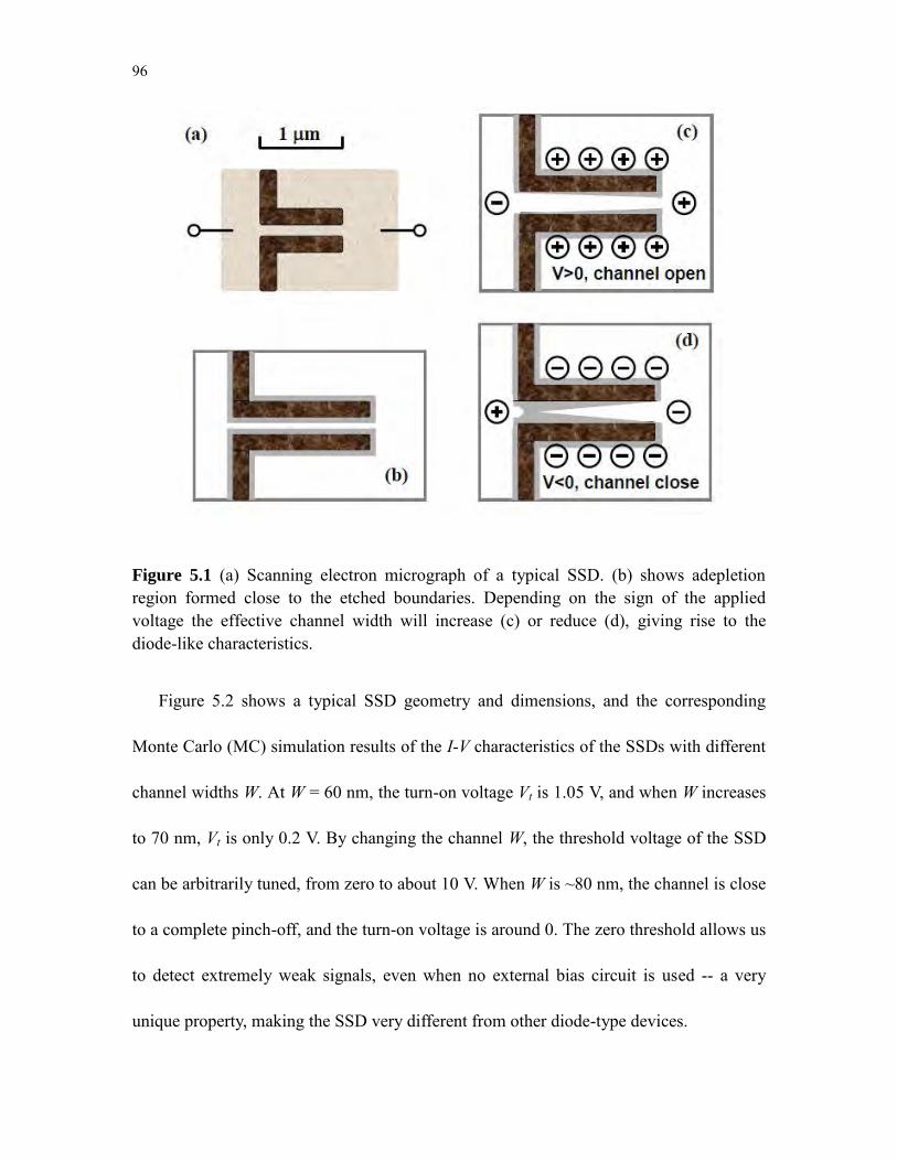
96
Figure 5.1 (a) Scanning electron micrograph of a typical SSD. (b) shows adepletion region formed close to the etched boundaries. Depending on the sign of the applied voltage the effective channel width will increase (c) or reduce (d), giving rise to the diode-like characteristics.
Figure 5.2 shows a typical SSD geometry and dimensions, and the corresponding
Monte Carlo (MC) simulation results of the I-V characteristics of the SSDs with different
channel widths W. At W = 60 nm, the turn-on voltage Vt is 1.05 V, and when W increases
to 70 nm, Vt is only 0.2 V. By changing the channel W, the threshold voltage of the SSD
can be arbitrarily tuned, from zero to about 10 V. When W is ~80 nm, the channel is close
to a complete pinch-off, and the turn-on voltage is around 0. The zero threshold allows us
to detect extremely weak signals, even when no external bias circuit is used -- a very
unique property, making the SSD very different from other diode-type devices.
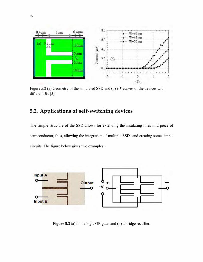
97
Figure 5.2 (a) Geometry of the simulated SSD and (b) I-V curves of the devices with different W. [5]
5.2. Applications of self-switching devices
The simple structure of the SSD allows for extending the insulating lines in a piece of
semiconductor, thus, allowing the integration of multiple SSDs and creating some simple
circuits. The figure below gives two examples:
Figure 5.3 (a) diode logic OR gate, and (b) a bridge rectifier.
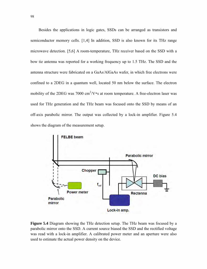
98
Besides the applications in logic gates, SSDs can be arranged as transistors and
semiconductor memory cells. [1,4] In addition, SSD is also known for its THz range
microwave detection. [5,6] A room-temperature, THz receiver based on the SSD with a
bow tie antenna was reported for a working frequency up to 1.5 THz. The SSD and the
antenna structure were fabricated on a GaAs/AlGaAs wafer, in which free electrons were
confined to a 2DEG in a quantum well, located 50 nm below the surface. The electron
mobility of the 2DEG was 7000 cm2/V•s at room temperature. A free-electron laser was
used for THz generation and the THz beam was focused onto the SSD by means of an
off-axis parabolic mirror. The output was collected by a lock-in amplifier. Figure 5.4
shows the diagram of the measurement setup.
Figure 5.4 Diagram showing the THz detection setup. The THz beam was focused by a parabolic mirror onto the SSD. A current source biased the SSD and the rectified voltage was read with a lock-in amplifier. A calibrated power meter and an aperture were also used to estimate the actual power density on the device.
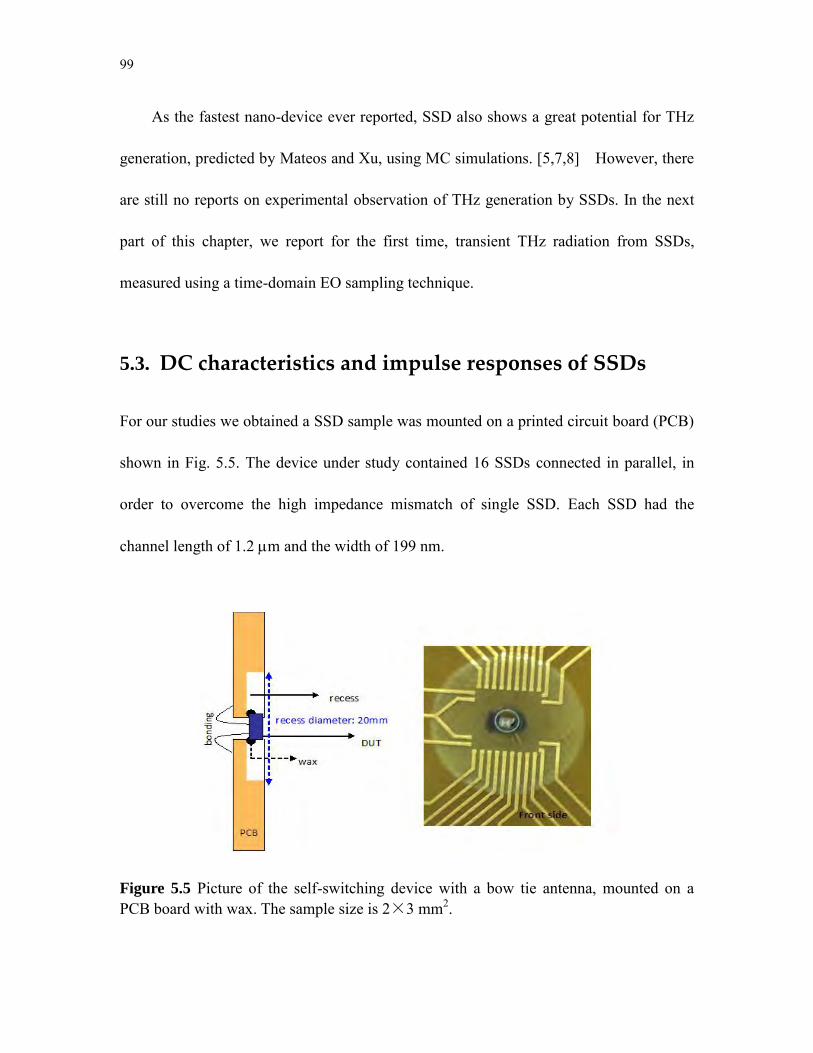
99
As the fastest nano-device ever reported, SSD also shows a great potential for THz
generation, predicted by Mateos and Xu, using MC simulations. [5,7,8] However, there
are still no reports on experimental observation of THz generation by SSDs. In the next
part of this chapter, we report for the first time, transient THz radiation from SSDs,
measured using a time-domain EO sampling technique.
5.3. DC characteristics and impulse responses of SSDs
For our studies we obtained a SSD sample was mounted on a printed circuit board (PCB)
shown in Fig. 5.5. The device under study contained 16 SSDs connected in parallel, in
order to overcome the high impedance mismatch of single SSD. Each SSD had the
channel length of 1.2 m and the width of 199 nm.
Figure 5.5 Picture of the self-switching device with a bow tie antenna, mounted on a PCB board with wax. The sample size is 2×3 mm2.
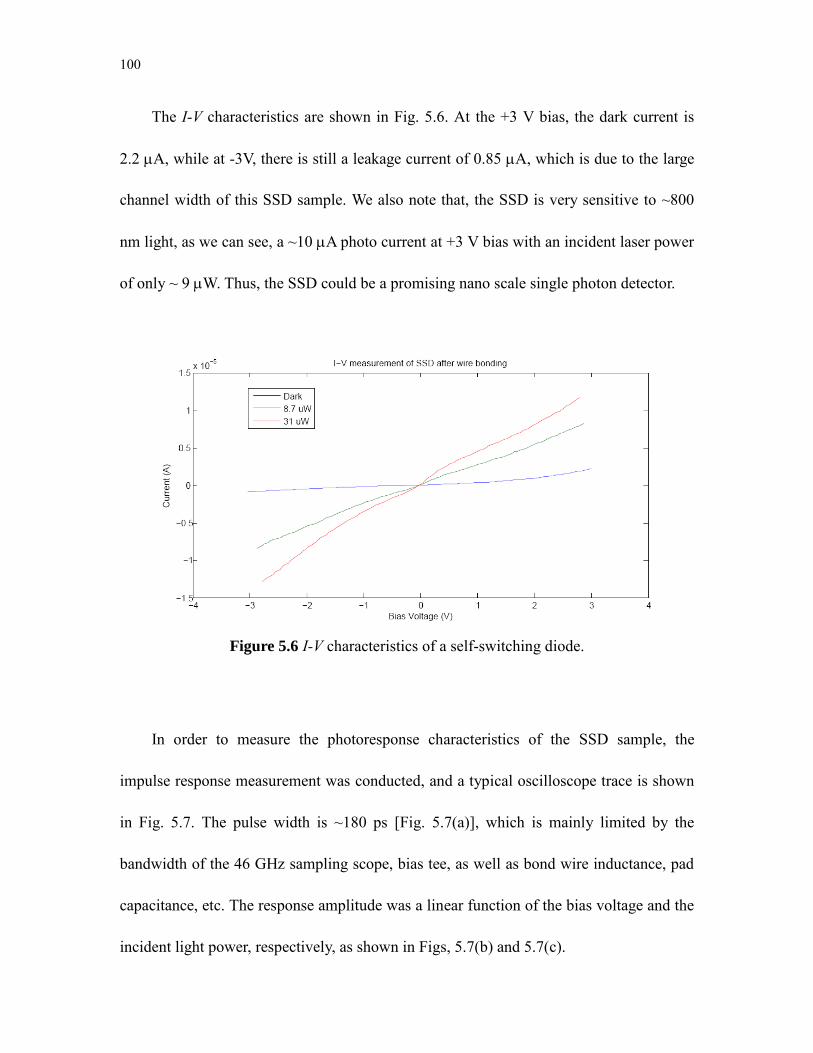
100
The I-V characteristics are shown in Fig. 5.6. At the +3 V bias, the dark current is
2.2 A, while at -3V, there is still a leakage current of 0.85 A, which is due to the large
channel width of this SSD sample. We also note that, the SSD is very sensitive to ~800
nm light, as we can see, a ~10 A photo current at +3 V bias with an incident laser power
of only ~ 9 W. Thus, the SSD could be a promising nano scale single photon detector.
Figure 5.6 I-V characteristics of a self-switching diode.
In order to measure the photoresponse characteristics of the SSD sample, the
impulse response measurement was conducted, and a typical oscilloscope trace is shown
in Fig. 5.7. The pulse width is ~180 ps [Fig. 5.7(a)], which is mainly limited by the
bandwidth of the 46 GHz sampling scope, bias tee, as well as bond wire inductance, pad
capacitance, etc. The response amplitude was a linear function of the bias voltage and the
incident light power, respectively, as shown in Figs, 5.7(b) and 5.7(c).
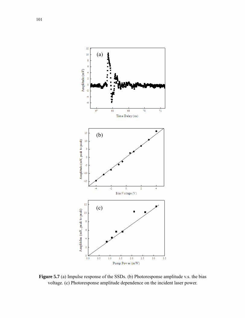
101
Figure 5.7 (a) Impulse response of the SSDs. (b) Photoresponse amplitude v.s. the bias voltage. (c) Photoresponse amplitude dependence on the incident laser power.
(a)
(b)
(c)
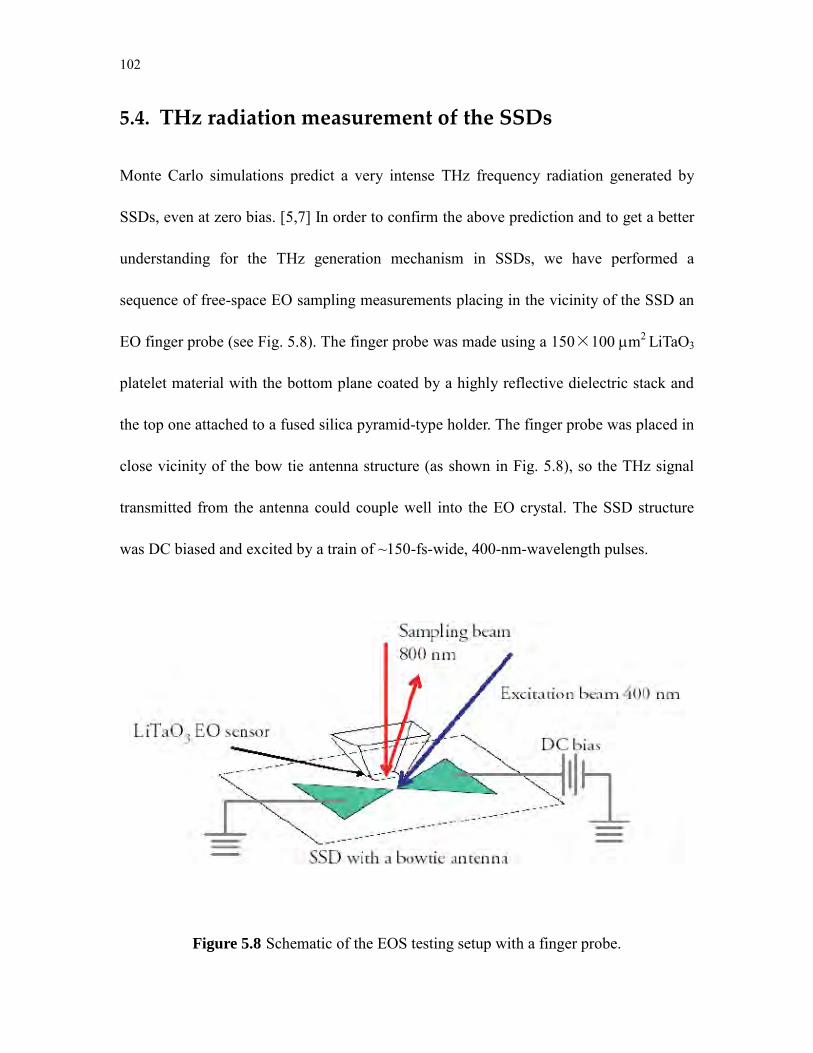
102
5.4. THz radiation measurement of the SSDs
Monte Carlo simulations predict a very intense THz frequency radiation generated by
SSDs, even at zero bias. [5,7] In order to confirm the above prediction and to get a better
understanding for the THz generation mechanism in SSDs, we have performed a
sequence of free-space EO sampling measurements placing in the vicinity of the SSD an
EO finger probe (see Fig. 5.8). The finger probe was made using a 150×100 m2 LiTaO3
platelet material with the bottom plane coated by a highly reflective dielectric stack and
the top one attached to a fused silica pyramid-type holder. The finger probe was placed in
close vicinity of the bow tie antenna structure (as shown in Fig. 5.8), so the THz signal
transmitted from the antenna could couple well into the EO crystal. The SSD structure
was DC biased and excited by a train of ~150-fs-wide, 400-nm-wavelength pulses.
Figure 5.8 Schematic of the EOS testing setup with a finger probe.
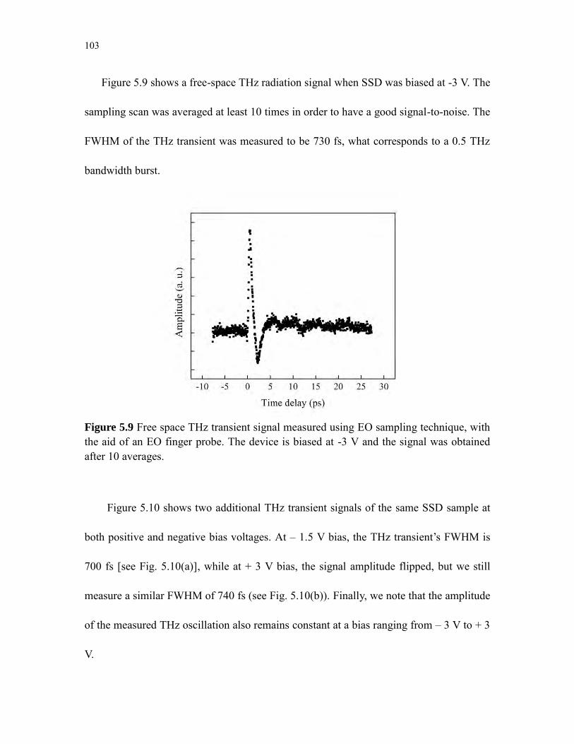
103
Figure 5.9 shows a free-space THz radiation signal when SSD was biased at -3 V. The
sampling scan was averaged at least 10 times in order to have a good signal-to-noise. The
FWHM of the THz transient was measured to be 730 fs, what corresponds to a 0.5 THz
bandwidth burst.
Figure 5.9 Free space THz transient signal measured using EO sampling technique, with the aid of an EO finger probe. The device is biased at -3 V and the signal was obtained after 10 averages.
Figure 5.10 shows two additional THz transient signals of the same SSD sample at
both positive and negative bias voltages. At – 1.5 V bias, the THz transient’s FWHM is
700 fs [see Fig. 5.10(a)], while at + 3 V bias, the signal amplitude flipped, but we still
measure a similar FWHM of 740 fs (see Fig. 5.10(b)). Finally, we note that the amplitude
of the measured THz oscillation also remains constant at a bias ranging from – 3 V to + 3
V.
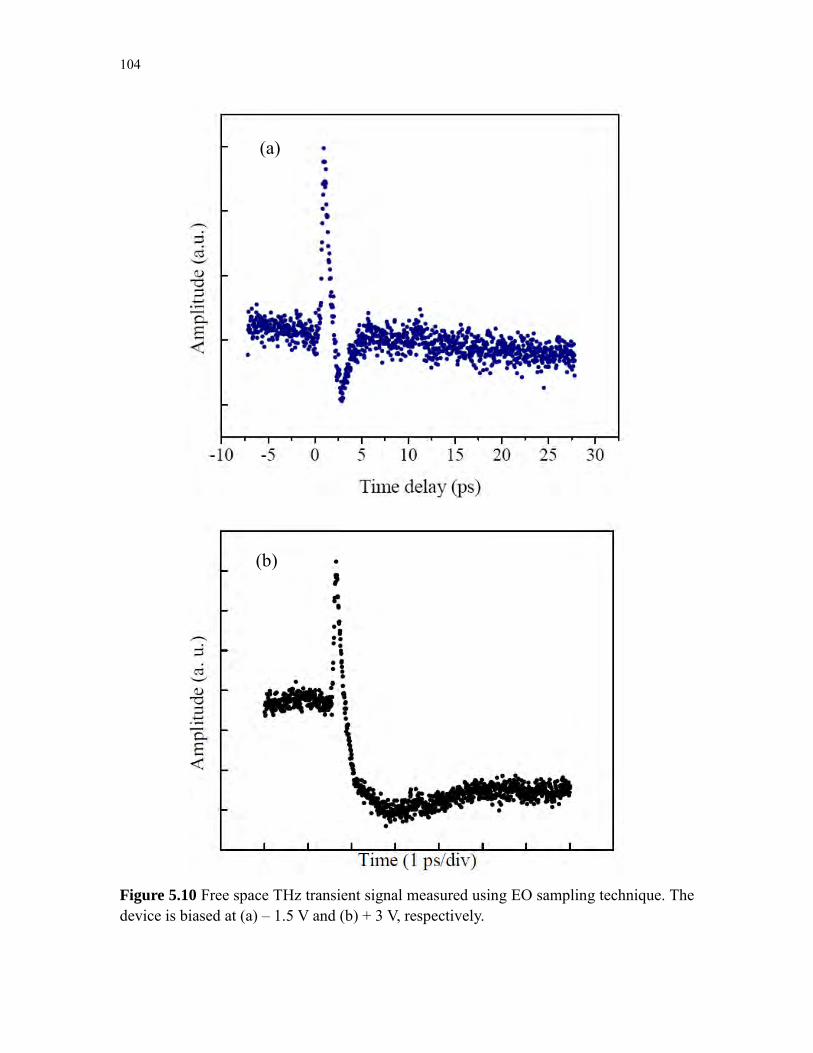
104
Figure 5.10 Free space THz transient signal measured using EO sampling technique. The device is biased at (a) – 1.5 V and (b) + 3 V, respectively.
(a)
(b)
105
Bibliography
[1] A. M. Song, M. Missous, P. Omling, A. R. Peaker, L, Samuelson, and W. Seifert,
Appl. Phys. Lett. 83, 1881 (2003).
[2] A. M. Song, I. Maximov, M. Missous, and W. Seifert, Physica E, 21, 1116 (2004).
[3] G. Farhi, E. Saracco, J. Beerens, D. Morris, S.A. Charlebois, and J.-P. Raskin,
Solid-State Electronics 51 1245 (2007).
[4] A. M. Song, M. Missous, P. Omling, I. Maximov, W. Seifert, and L. Samuelson,
Applied Physics Letters, 86, 042106 (2005).
[5] J. Mateos, A.M. Song, B.G. Vasallo, D. Pardo1, and T. González, Proceedings of
SPIE, 5838 (2005).
[6] Claudio Balocco, Shahrir R. Kasjoo, Xiaofeng Lu, Linqing Zhang, Yasaman Alimi,
Stephan Winnerl, and Aimin M. Song, Appl. Phys. Lett. 98, 223501 (2011).
[7] K. Y. Xu, X. F. Lu, A. M. Song, and G. Wang, Appl. Phys. Lett. 92, 163503 (2008).
[8] K. Y. Xu, G. Wang and A. M. Song, Appl. Phys. Lett. 93, 233506 (2008).
106
6. Conclusions
6.1. Thesis summary
This thesis studied the ultrafast carrier and phonon dynamics in Ga-based III-V
semiconductor materials, such as, GaAs, GaN and AlGaN, and the THz frequency range
response of the related devices. The achievements throughout this research can be
categorized into the five parts:
We have performed all-optical experiments aimed at generation and detection of
CAPs in GaN single crystals, and accurately determined the intrinsic CAP decoherence
time. In this work, we studied the CAPs generation and detection mechanism with both
one- and two-color pump-probe spectroscopies. We have accurately measured the CAP
lifetime using a two-side testing geometry and the lifetime was 80±3 ns in GaN single
crystals at room temperature.
In the second part, we focused on the investigation of NLO properties of AlGaN
single crystals, using a MPA technique with a non-traditional two-color femtosecond
pump-probe approach. It was found that two different processes contributed to the
probe-beam ∆T/T transients measured in our experiments. The first was the 310-fs-wide
correlation signal, observed near the zero-delay point, and corresponded to the TPA
correlation process involving a simultaneous absorption of one UV pump photon and one
107
SHG photon from the probe beam. The second component was the well-studied
relaxation dynamics of photo-excited carriers (electron-phonon relaxation and
electron-hole recombination and trapping). We studied the correlation and relaxation
signals amplitude dependences on the pump power intensity (with the probe beam
intensity constant) and modeled it with a nondegenerate TPA process. We also
demonstrated the spectral dependence of the TPA coefficient, within our laser tuning
range, agreed well with the Sheik-Bahae and Hutchings theory.
The third part was devoted to time-domain EO characterization of a GaN OEIC
structure containing an integrated MSM-type PD element and a MESFET. The PD
showed a pulse response of 0.9 ps FWHM, corresponding to bandwidth of 410 GHz. At
low frequencies, our OEIC showed a tenfold higher response than just the MSM PD and
it exhibited the power gain up to 150 GHz. These results show that GaN-based devices
are a very promising candidates for ultrafast UV optoelectronic integrated circuits.
In the fourth part, we measured the performance of a high-speed, high repletion rate,
epitaxially grown GaAs meso-structured PDs. Our, so-called, free-standing PDs featured
an extremely low dark current of only 2×10⁻⁹ A and responsivity of 4.4 mA/W at 30 V. Its
intrinsic photon detection efficiency was ~ 7%. The time-domain EO sampling studies
showed that the PD had a very fast, ~ 310 fs wide, intrinsic photoresponse, corresponding
to a bandwidth of 1.4 THz. With the double-pulse excitation setup, the PD was tested for
successful operation at ~1 THz repetition rate. We also note that, with the unique
fabrication approach pioneered by the Jülich Research Center, Jülich, Germany, the
108
freestanding structures can be placed at virtually any point on a test circuit, making them
very promising for hybrid circuitry for THz electronic and photonic applications.
The last element of the thesis was devoted to the THz radiation measurements of a
novel nano-electronic device–SSD. We observed, for the first time, a transient (~
700-fs-wide) THz radiation signal from the SSD, biased at various voltages, from – 3 V
to + 3 V. The THz emission mechanism of the device still needs further investigation.
6.2. Future work
The first AlGaN single crystals have been synthesized by our collaborators very recently
and, their fundamental physical properties still remain unclear or unexplored. From both
the fundamental physics point-of-view and potential applications of AlGaN and other
nitride semiconductors require extensive studies of their fundamental properties are
needed. We have just started the process by performing detailed characterization on
AlxGa1-xN with x = 0.86, such as the EG determination, NLO property measurement and
non-equilibrium carrier dynamic characterization. Systematical optical studies of
AlxGa1-xN materials with x in the entire 0.5 – 1 range are required, as well as observation
of the behavior of both optical and acoustic phonon modes as a function of Al
composition. The influence of the Al composition on optical properties of this ternary
alloy should contribute to our understanding of the fundamental properties of this
advanced material.
Another interesting topic to explore is the origin of super fast response time and THz
109
repetition rate in PDs based on epitaxially-grown single crystal GaAs meso-structures.
The ~500 nm thickness of our samples seems to play an important role contributing to the
~200-fs electron-hole recombination time. Time-resolved photoresponse measurements
on samples with different thicknesses will be needed to confirm our conclusion
experimentally. It is also very interesting to perform a comparative series of
measurements on LT-GaAs specimens and directly identify the dominant factors, such as,
e.g., trapping of the overall ultrafast relaxation process.
Finally, although, we have observed for the first time, the transient THz radiation
signal from nanostructured SSDs, the actual THz generation mechanism remains not fully
understood, despite extensive MC simulations. More experiments and systematic studies
of the SSD samples with different channel length and width are required. Furthermore,
preliminary research shows that the SSD is extremely sensitive for 800 nm light. It is
interesting to explore the SSD’s spectral detection efficiency and, possibly, purse novel
applications, such as, single optical photon detection.


![AN EQUILIBRIUM CHARACTERIZATION OF THE TERM … · AN EQUILIBRIUM CHARACTERIZATION OF THE TERM ... (1969)] by a stochastic differential equation ... Solutions of partial differential](https://img.pdfslide.us/doc/110x75/5b580bee7f8b9aec628bd80b/an-equilibrium-characterization-of-the-term-an-equilibrium-characterization.jpg)