Embed Size (px)
Citation preview
RF to Digital (RF2D™) Data Converter Modules & RF Overview
Tim Fountain Business Segment Manager, DCM 503-816-2756, [email protected]
Agenda
Introduction to the Data Converter Modules Business – Business Principles
– Technology Introduction
– Reference Designs
FPGA DRFM prototyping system
RF to Digital (RF2D)
Tektronix Proprietary 2

Tek Products - Enabled by Leadership Technology
Key Enabling Technology
Performance
Oscilloscope 20 GHz RTSA Handheld
Spectrum
Analyzer
Multi-Domain
Oscilloscope
3
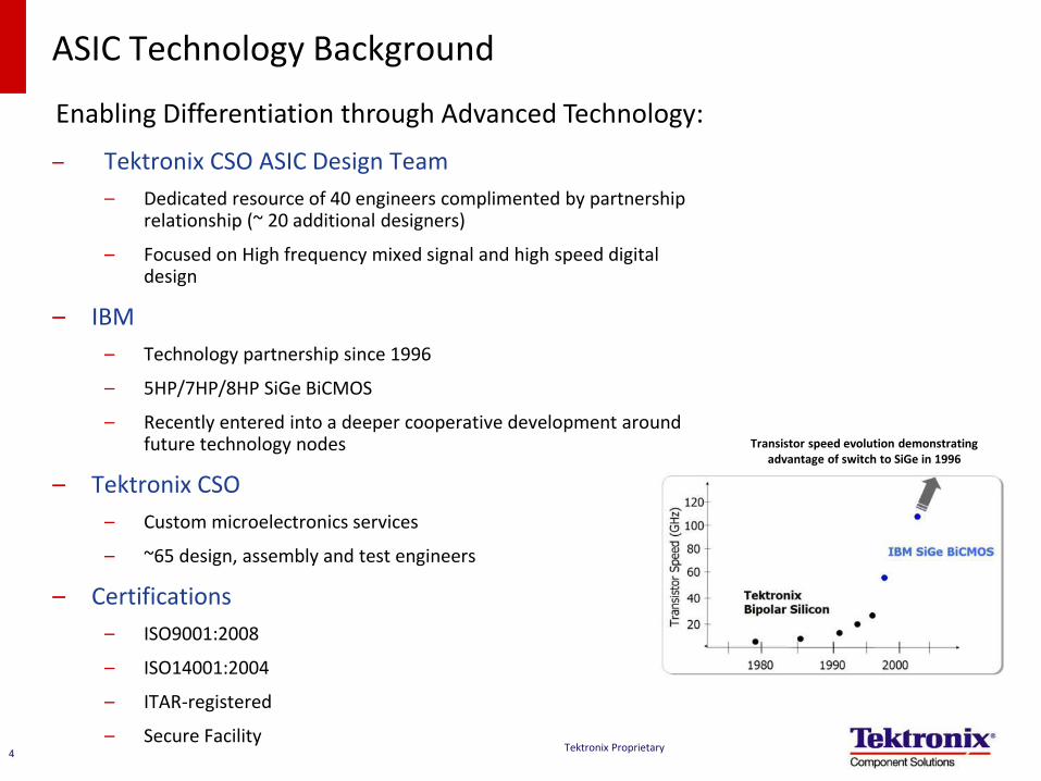
ASIC Technology Background
– Tektronix CSO ASIC Design Team
– Dedicated resource of 40 engineers complimented by partnership relationship (~ 20 additional designers)
– Focused on High frequency mixed signal and high speed digital design
– IBM
– Technology partnership since 1996
– 5HP/7HP/8HP SiGe BiCMOS
– Recently entered into a deeper cooperative development around future technology nodes
– Tektronix CSO
– Custom microelectronics services
– ~65 design, assembly and test engineers
– Certifications
– ISO9001:2008
– ISO14001:2004
– ITAR-registered
– Secure Facility
Transistor speed evolution demonstrating advantage of switch to SiGe in 1996
Enabling Differentiation through Advanced Technology:
Tektronix Proprietary 4
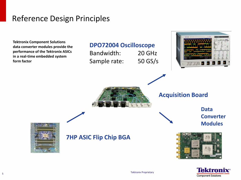
Reference Design Principles
DPO72004 Oscilloscope Bandwidth: 20 GHz Sample rate: 50 GS/s
7HP ASIC Flip Chip BGA
Acquisition Board
Tektronix Component Solutions data converter modules provide the performance of the Tektronix ASICs in a real-time embedded system form factor
Data Converter Modules
Tektronix Proprietary 5
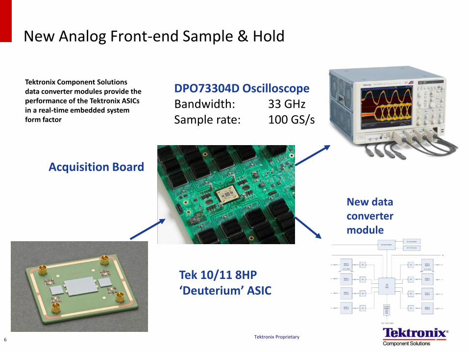
New Analog Front-end Sample & Hold
DPO73304D Oscilloscope Bandwidth: 33 GHz Sample rate: 100 GS/s
Tek 10/11 8HP ‘Deuterium’ ASIC
Acquisition Board
Tektronix Component Solutions data converter modules provide the performance of the Tektronix ASICs in a real-time embedded system form factor
New data converter module
Tektronix Proprietary 6
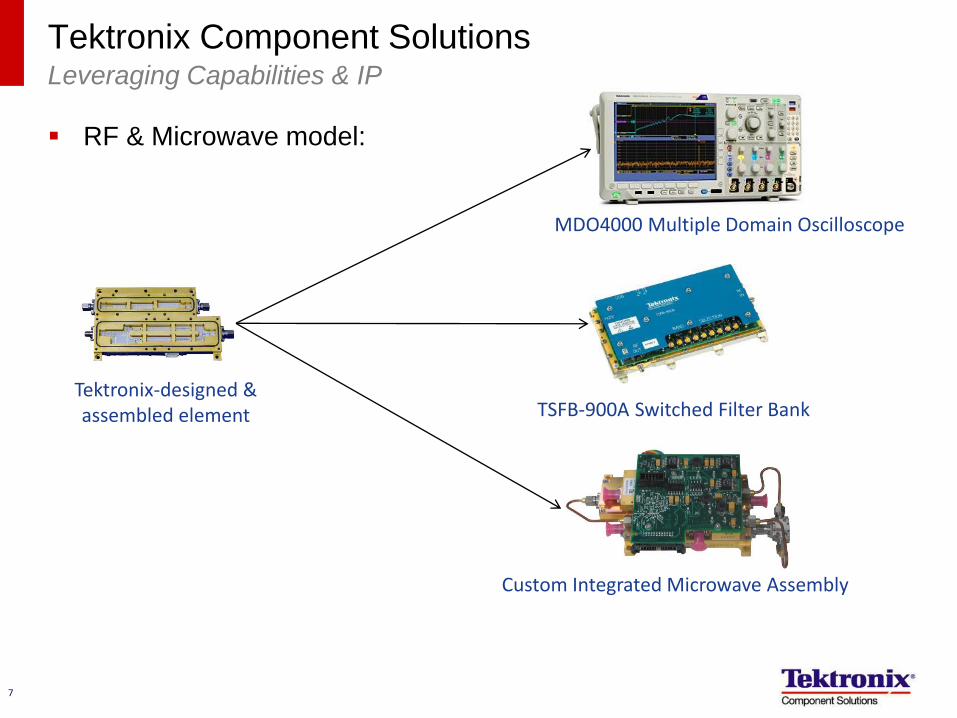
Tektronix Component Solutions Leveraging Capabilities & IP
RF & Microwave model:
TSFB-900A Switched Filter Bank Tektronix-designed & assembled element
Custom Integrated Microwave Assembly
MDO4000 Multiple Domain Oscilloscope
7
0
2
4
6
8
10
12
14
16
18
20
10 KHz 100 KHz 1 MHz 10 MHz 100 MHz 1 GHz 10 GHz 100 Ghz
Analog Input Frequency (Hz)
ENO
B
< 0.1 W
0.1 W < 0.5W
0.5 W < 1 W
1 W < 2 W
2 W < 5 W
> 5 W
ISSCC 2006
VLSI Ckts 2006
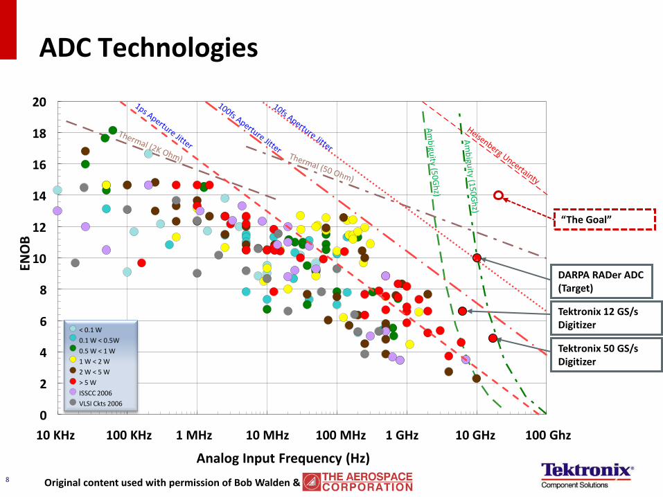
ADC Technologies
Tektronix 12 GS/s Digitizer
Tektronix 50 GS/s Digitizer
DARPA RADer ADC (Target)
Original content used with permission of Bob Walden &
“The Goal”
8
Provides access to Tektronix Data Converter technology:
– Without the investment required for a custom module
– For immediate prototyping and application tests
– To help determine and evaluate specifications for a custom module
Modules are:
– Designed for use as a production solution
– Must comply with US export requirements
Data Converter Module Reference Designs
Tektronix Proprietary 9
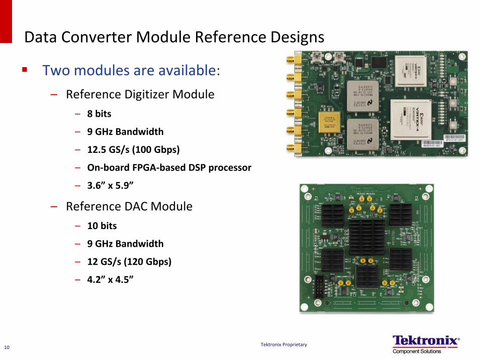
Two modules are available:
– Reference Digitizer Module
– 8 bits
– 9 GHz Bandwidth
– 12.5 GS/s (100 Gbps)
– On-board FPGA-based DSP processor
– 3.6” x 5.9”
– Reference DAC Module
– 10 bits
– 9 GHz Bandwidth
– 12 GS/s (120 Gbps)
– 4.2” x 4.5”
Data Converter Module Reference Designs
Tektronix Proprietary 10
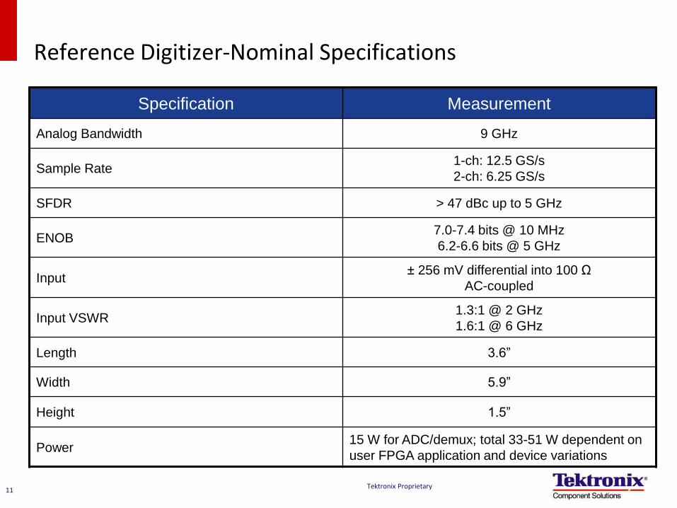
Specification Measurement
Analog Bandwidth 9 GHz
Sample Rate 1-ch: 12.5 GS/s
2-ch: 6.25 GS/s
SFDR > 47 dBc up to 5 GHz
ENOB 7.0-7.4 bits @ 10 MHz
6.2-6.6 bits @ 5 GHz
Input ± 256 mV differential into 100 Ω
AC-coupled
Input VSWR 1.3:1 @ 2 GHz
1.6:1 @ 6 GHz
Length 3.6”
Width 5.9”
Height 1.5”
Power 15 W for ADC/demux; total 33-51 W dependent on
user FPGA application and device variations
Reference Digitizer-Nominal Specifications
Tektronix Proprietary 11
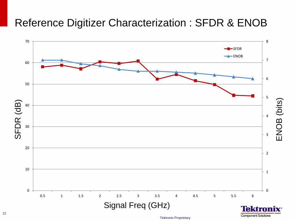
Reference Digitizer Characterization : SFDR & ENOB
Tektronix Proprietary
12
0
1
2
3
4
5
6
7
8
0
10
20
30
40
50
60
70
0.5 1 1.5 2 2.5 3 3.5 4 4.5 5 5.5 6
SFDR
ENOB
SF
DR
(d
B)
EN
OB
(b
its)
Signal Freq (GHz)
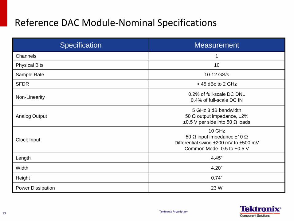
Specification Measurement
Channels 1
Physical Bits 10
Sample Rate 10-12 GS/s
SFDR > 45 dBc to 2 GHz
Non-Linearity 0.2% of full-scale DC DNL
0.4% of full-scale DC IN
Analog Output
5 GHz 3 dB bandwidth
50 Ω output impedance, ±2%
±0.5 V per side into 50 Ω loads
Clock Input
10 GHz
50 Ω input impedance ±10 Ω
Differential swing ±200 mV to ±500 mV
Common Mode -0.5 to +0.5 V
Length 4.45”
Width 4.20”
Height 0.74”
Power Dissipation 23 W
Reference DAC Module-Nominal Specifications
Tektronix Proprietary 13
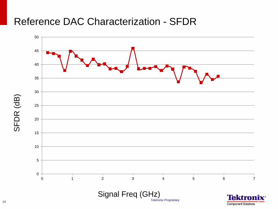
Reference DAC Characterization - SFDR
Tektronix Proprietary 14
0
5
10
15
20
25
30
35
40
45
50
0 1 2 3 4 5 6 7
SF
DR
(d
B)
Signal Freq (GHz)
Agenda
Introduction to the DCM Business – Business Principles
– Technology Introduction
– Reference Designs
FPGA DRFM prototyping system
RF to Digital
Tektronix Proprietary 15
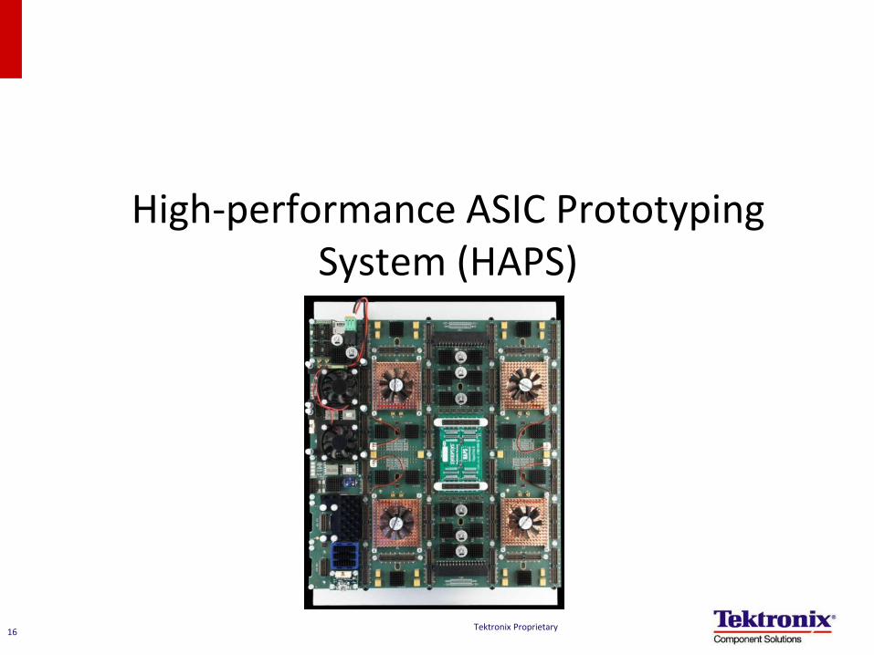
High-performance ASIC Prototyping System (HAPS)
Tektronix Proprietary 16
HAPS Intro
Core FPGA hardware from Synopsys (www.synopsys.com)
Quick & easy prototyping of complex FPGA applications
Rich IP support
Support for up to 4 Digitizers or DAC interposers or combinations thereof – System bandwidths of up to 400 Gb/s (input) & 480 Gb/s (output)
– 4.5, 9 or 18 million gates
Gives customer’s access to Tektronix’ digitizer and DAC technology – Complete packaged, validated design giving faster time to market
Scalable architecture with high-speed FPGA to FPGA busses – Expandability
Wide array of peripheral daughterboard options using HapsTrak standard to connect to industry standard busses and peripherals
Off the shelf hardware
Tektronix Proprietary
17
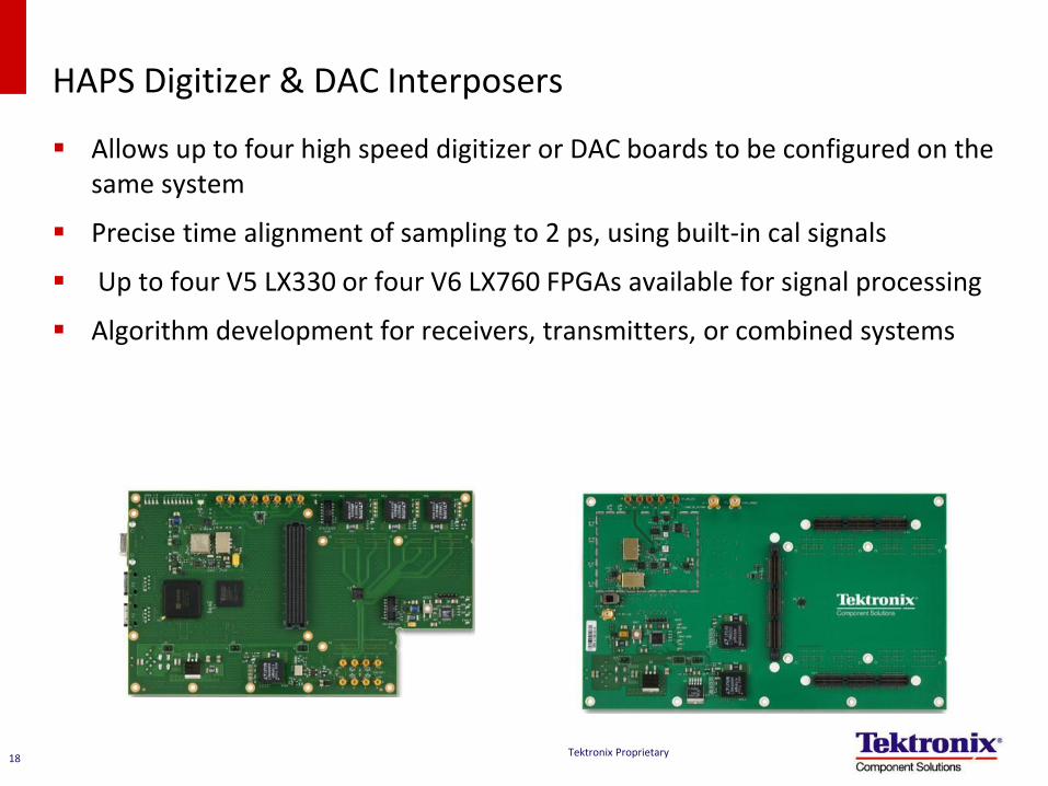
HAPS Digitizer & DAC Interposers
Allows up to four high speed digitizer or DAC boards to be configured on the same system
Precise time alignment of sampling to 2 ps, using built-in cal signals
Up to four V5 LX330 or four V6 LX760 FPGAs available for signal processing
Algorithm development for receivers, transmitters, or combined systems
Tektronix Proprietary 18
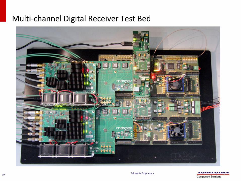
Multi-channel Digital Receiver Test Bed
Tektronix Proprietary 19
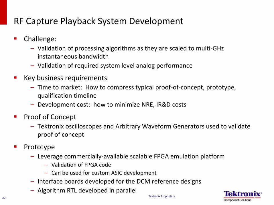
RF Capture Playback System Development
Challenge: – Validation of processing algorithms as they are scaled to multi-GHz
instantaneous bandwidth
– Validation of required system level analog performance
Key business requirements – Time to market: How to compress typical proof-of-concept, prototype,
qualification timeline
– Development cost: how to minimize NRE, IR&D costs
Proof of Concept – Tektronix oscilloscopes and Arbitrary Waveform Generators used to validate
proof of concept
Prototype – Leverage commercially-available scalable FPGA emulation platform
– Validation of FPGA code
– Can be used for custom ASIC development
– Interface boards developed for the DCM reference designs
– Algorithm RTL developed in parallel Tektronix Proprietary
20
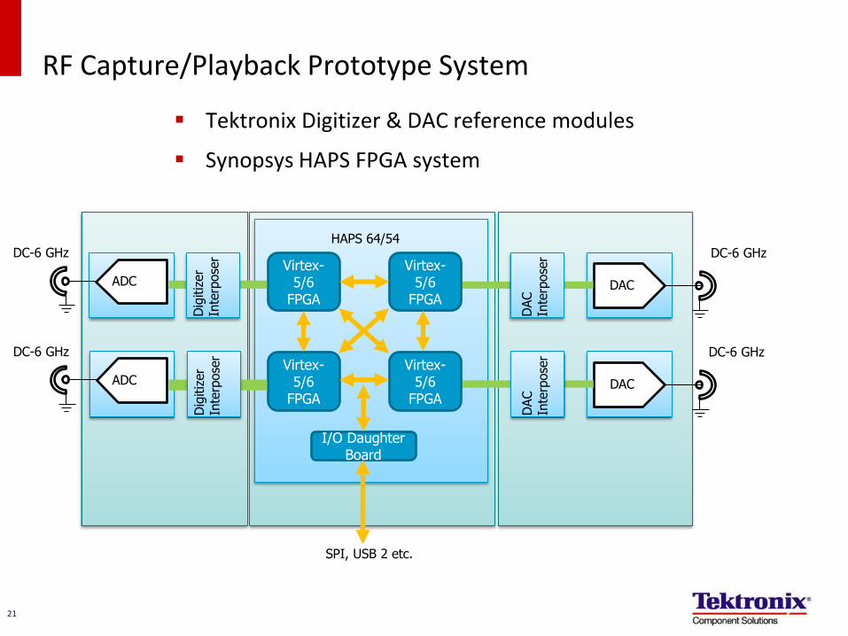
RF Capture/Playback Prototype System
Tektronix Digitizer & DAC reference modules
Synopsys HAPS FPGA system
21
ADC Virtex-
5/6 FPGA
DC-6 GHz HAPS 64/54
Virtex-5/6
FPGA
Virtex-5/6
FPGA
Virtex-5/6
FPGA
DAC
DC-6 GHz
Dig
itiz
er
In
terp
ose
r
DAC
Inte
rpose
r
ADC
DC-6 GHz
Dig
itiz
er
In
terp
ose
r
DAC
DC-6 GHz
DAC
Inte
rpose
r
I/O Daughter Board
SPI, USB 2 etc.
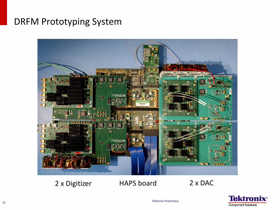
DRFM Prototyping System
22
2 x Digitizer HAPS board 2 x DAC
Tektronix Proprietary
Agenda
Introduction to the DCM Business – Business Principles
– Technology Introduction
– Reference Designs
FPGA DRFM prototyping system
RF to Digital (RF2D)
Tektronix Proprietary 23
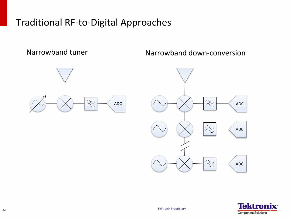
Traditional RF-to-Digital Approaches
24
Narrowband tuner
ADC ADC
ADC
ADC
Narrowband down-conversion
Tektronix Proprietary
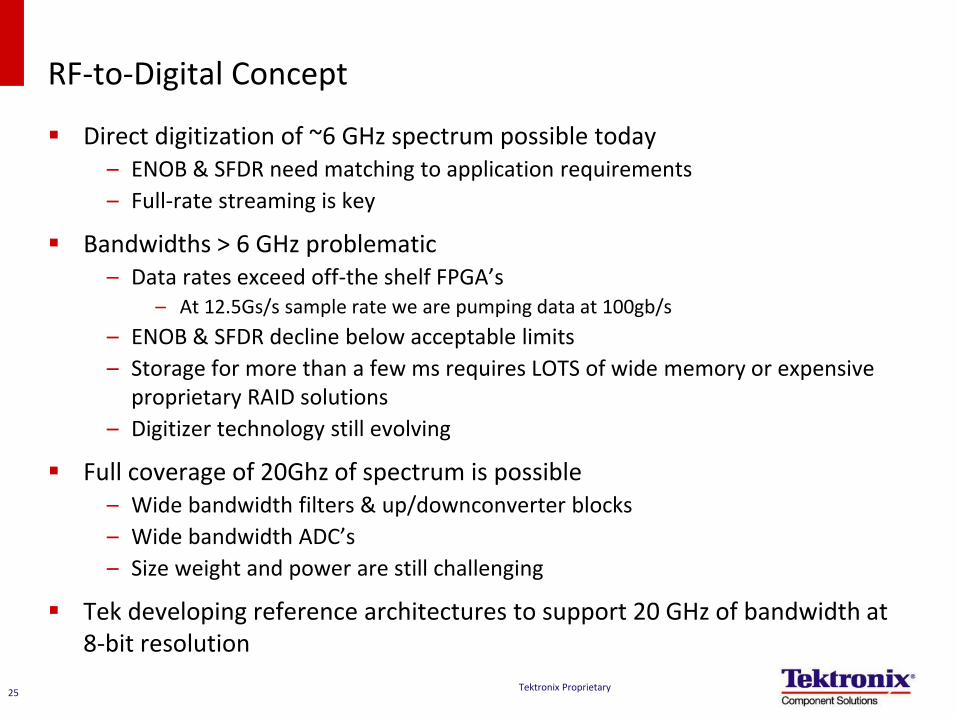
RF-to-Digital Concept
Direct digitization of ~6 GHz spectrum possible today – ENOB & SFDR need matching to application requirements
– Full-rate streaming is key
Bandwidths > 6 GHz problematic – Data rates exceed off-the shelf FPGA’s
– At 12.5Gs/s sample rate we are pumping data at 100gb/s
– ENOB & SFDR decline below acceptable limits
– Storage for more than a few ms requires LOTS of wide memory or expensive proprietary RAID solutions
– Digitizer technology still evolving
Full coverage of 20Ghz of spectrum is possible – Wide bandwidth filters & up/downconverter blocks
– Wide bandwidth ADC’s
– Size weight and power are still challenging
Tek developing reference architectures to support 20 GHz of bandwidth at 8-bit resolution
Tektronix Proprietary 25
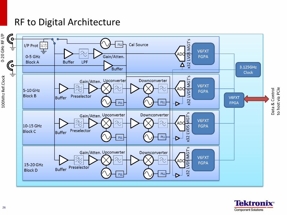
RF to Digital Architecture
26
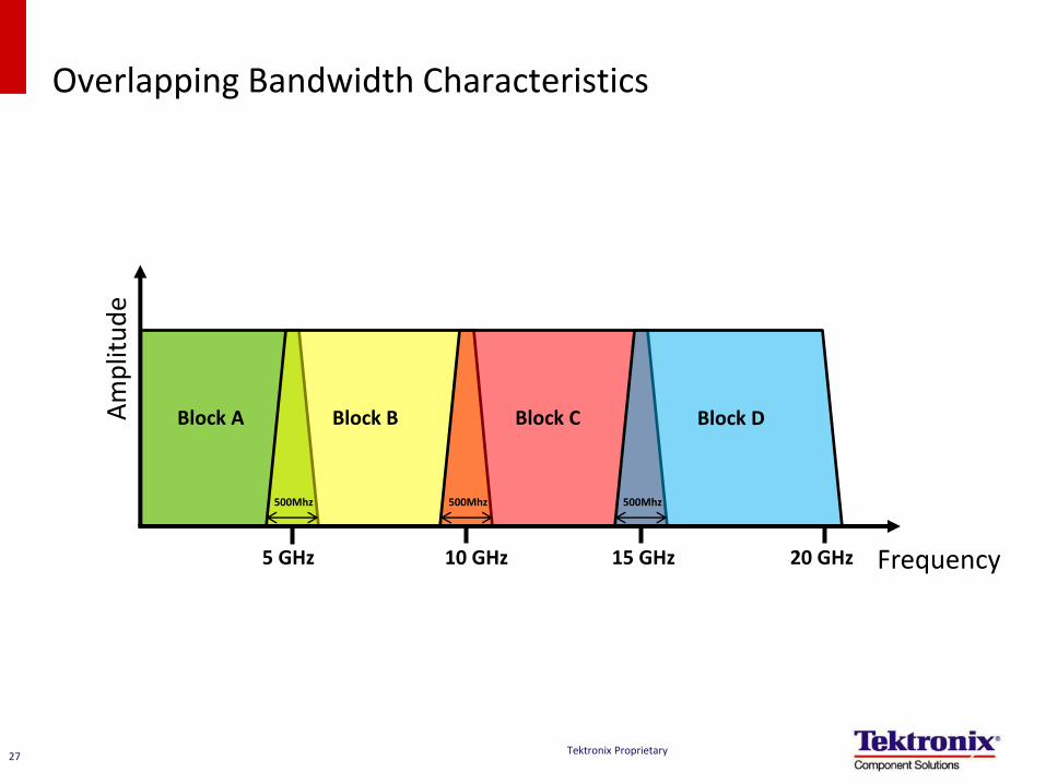
Overlapping Bandwidth Characteristics
Tektronix Proprietary 27
5 GHz 10 GHz 15 GHz 20 GHz
500Mhz 500Mhz 500Mhz
Block A Block B Block C Block D
Frequency
Am
plit
ud
e
RF/Microwave Module & Sub-Assembly Experience
RF/μWave solutions for Tek
– Sampling & TDR modules (DC to 70GHz)
– HF Broadband Probes (DC to >20GHz)
– Spectrum Analyzer modules & sub-assemblies
– (RTBW > 100MHz, Freq Range > 20GHz)
Custom Functional Blocks:
– Band Switches
– Switched Filter Banks
– Mixers, converter blocks
– Frequency Doublers
– Frequency Synthesizers
– DROs / LOs / PLLs
– IF Amplifiers
– Broadband Amplifiers
– Clock Recovery Modules
28
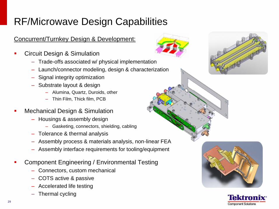
RF/Microwave Design Capabilities
Concurrent/Turnkey Design & Development:
Circuit Design & Simulation
– Trade-offs associated w/ physical implementation
– Launch/connector modeling, design & characterization
– Signal integrity optimization
– Substrate layout & design
– Alumina, Quartz, Duroids, other
– Thin Film, Thick film, PCB
Mechanical Design & Simulation
– Housings & assembly design
– Gasketing, connectors, shielding, cabling
– Tolerance & thermal analysis
– Assembly process & materials analysis, non-linear FEA
– Assembly interface requirements for tooling/equipment
Component Engineering / Environmental Testing
– Connectors, custom mechanical
– COTS active & passive
– Accelerated life testing
– Thermal cycling
29
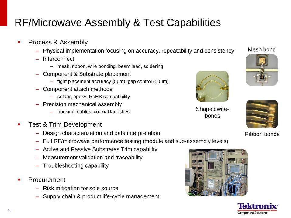
RF/Microwave Assembly & Test Capabilities
Process & Assembly
– Physical implementation focusing on accuracy, repeatability and consistency
– Interconnect
– mesh, ribbon, wire bonding, beam lead, soldering
– Component & Substrate placement
– tight placement accuracy (5μm), gap control (50μm)
– Component attach methods
– solder, epoxy, RoHS compatibility
– Precision mechanical assembly
– housing, cables, coaxial launches
Test & Trim Development
– Design characterization and data interpretation
– Full RF/microwave performance testing (module and sub-assembly levels)
– Active and Passive Substrates Trim capability
– Measurement validation and traceability
– Troubleshooting capability
Procurement
– Risk mitigation for sole source
– Supply chain & product life-cycle management
Mesh bond
Shaped wire-
bonds
Ribbon bonds
30
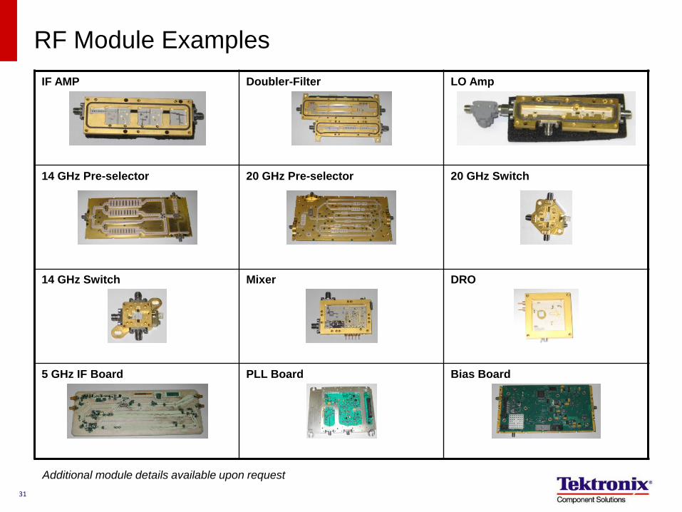
IF AMP Doubler-Filter LO Amp
14 GHz Pre-selector 20 GHz Pre-selector 20 GHz Switch
14 GHz Switch Mixer DRO
5 GHz IF Board PLL Board Bias Board
Additional module details available upon request
31
RF Module Examples
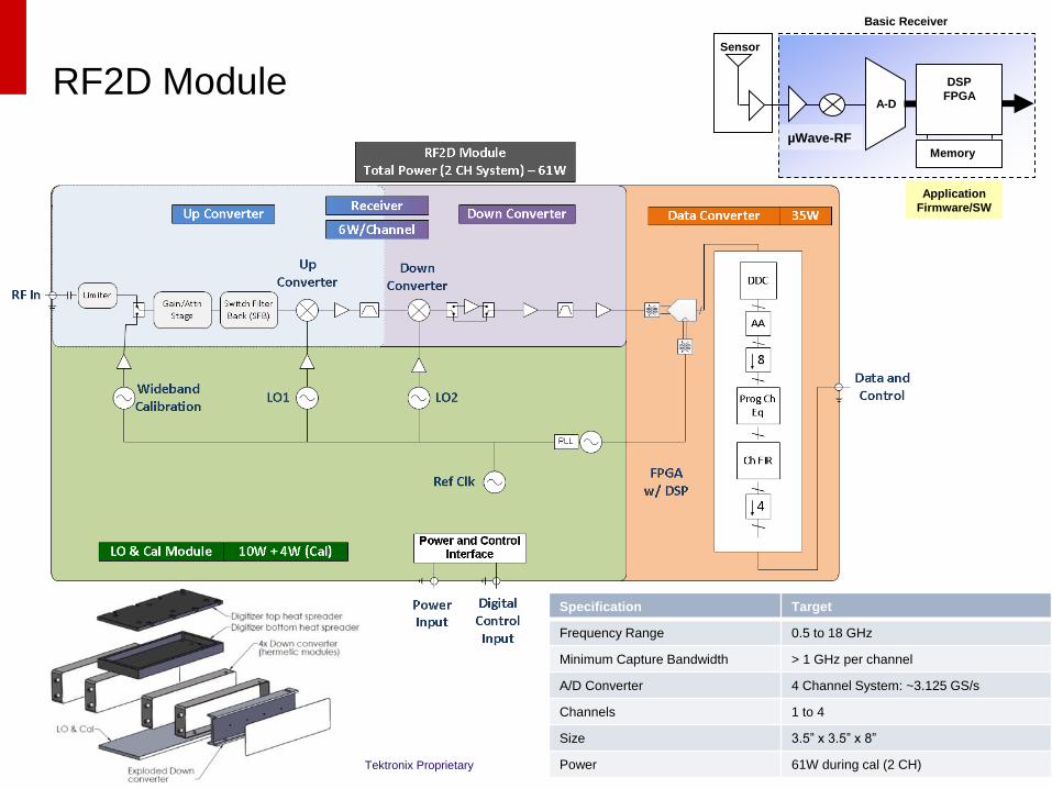
RF2D Module
Tektronix Proprietary
DSP
FPGA
Memory
Sensor
A-D
Application
Firmware/SW
µWave-RF
Basic Receiver
Specification Target
Frequency Range 0.5 to 18 GHz
Minimum Capture Bandwidth > 1 GHz per channel
A/D Converter 4 Channel System: ~3.125 GS/s
Channels 1 to 4
Size 3.5” x 3.5” x 8”
Power 61W during cal (2 CH)
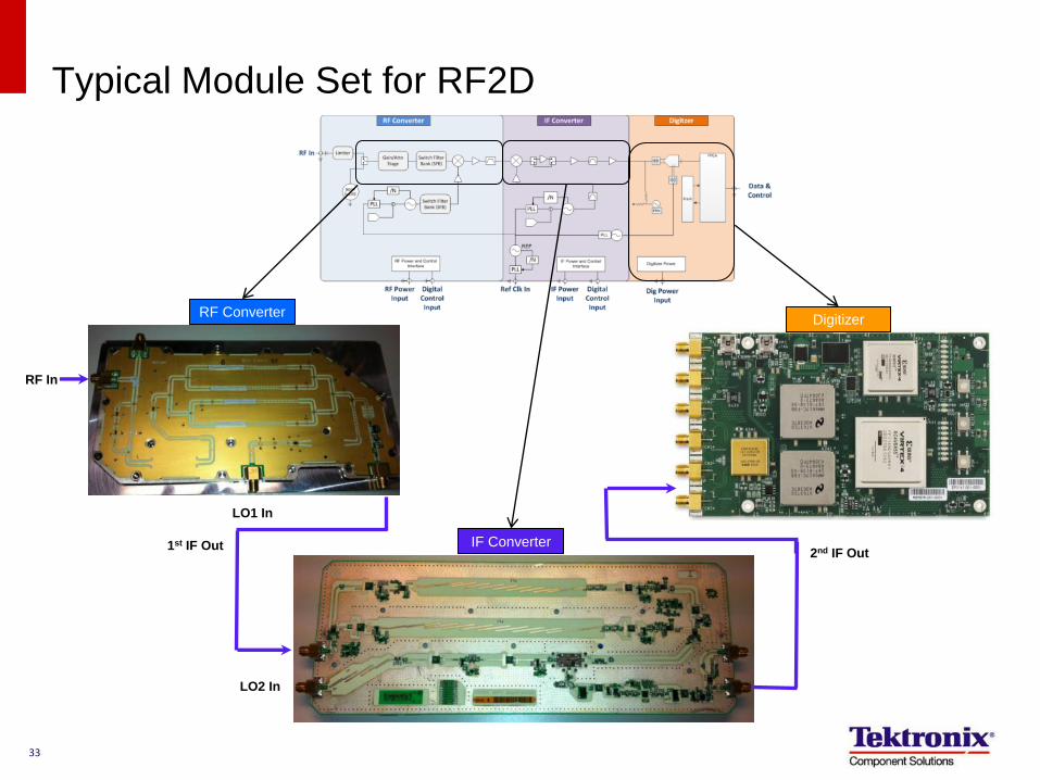
Typical Module Set for RF2D
RF In
LO1 In
1st IF Out
LO2 In
2nd IF Out
RF Converter
IF Converter
Digitizer
33
Summary
Providing a path to leverage core Tektronix technology for use in
RF/μWave mil/aero applications
– ASICs, Custom hardware development, RF design, packaging,
component-level test & processing algorithms
Equivalence between Tektronix Instruments, instrument-grade
functional elements and custom assemblies provides
– Reduction of Risk, Schedule & Costs
Focus on C-SWaP with wide-band capability
34
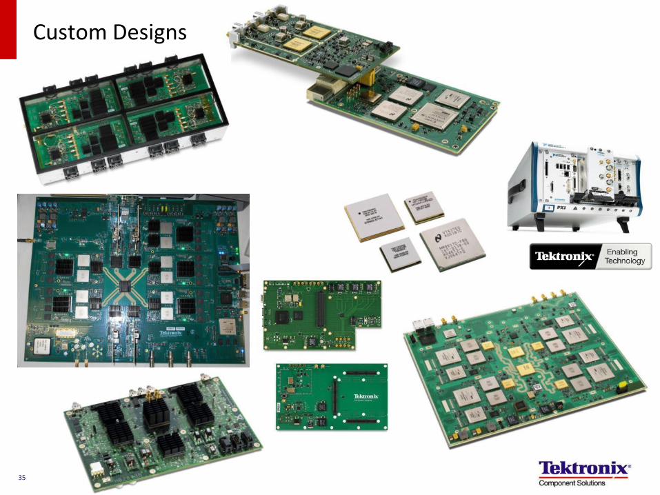
Custom Designs
35
Future possible developments
Miniaturization of RF components to address C-SWAP requirements
Direct connect Tek-204 Digitizer to FPGA
– Utilize SERDES on FPGA to eliminate DEMUX and reduce size/power/complexity
Multi Chip Module (MCM)
– Combine ADC, DEMUX & CAL FPGA on single chip
Low-latency DEMUX
New FPGA or XILINX ZYNQ on new ref digitizer
Higher analog bandwidth designs utilizing Tek 10/11 ASIC
– Interleave multiple Tek-204’s, 8 ADC’s would give 100Gs/s, 33GHz B/W
Higher resolution through gain ranging ADC’s
– Target is 8 ENOB (10 native) at ~3GHz of Bandwidth
– Still in research
Rugged modular VPX module
– Designed for DRFM/EW/SIGINT applications
– Flexible ADC/DAC sites – interchangeable 8, 10, 12 14+ bit designs
– Deep memory
– V6 FPGA
36
Summary You can have low power, high bandwidth OR high resolution
– Unfortunately you only get to pick one attribute at a time!
– Leading edge research focusing on 10 bits ENOB @ 10 GHz
Capable of supplying a complete RF2D solution
Capable of delivering full custom Integrated
Microwave Assemblies (IMAs)
Providing a path to leverage core Tektronix technology for use in embedded mil/aero applications
– ASICs, Custom hardware development, RF design, packaging, component-level test & processing algorithms
Equivalence between Tektronix Instruments, Reference Designs, ASICs and Test beds helps
– Reduce Risk, Schedule & Costs
Tek Components custom developments – Monolithic VME board with digitizer and larger FPGA
– Low-latency digitizer with larger FPGA
– Collaborated with National Instruments on PXIe digitizer
– Single module tunable 4-channel RF front-end with digitizers
– 17 GHz bandwidth (42 GS/s) monolithic digitizer
– RF to digital wide-bandwidth digitizer modules
37
Tektronix Proprietary