Embed Size (px)
Citation preview
THESIS FOR THE DEGREE OF LICENTIATE OF ENGINEERING
THz Ultra-wideband Passive Devices:
Design, Simulation and Characterization
Cristian Daniel López
Department of Space, Earth and Environment
CHALMERS UNIVERSITY OF TECHNOLOGY
Gothenburg, Sweden 2021

ii
THz Ultra-wideband Passive Devices:
Design, Simulation and Characterization
Cristian Daniel López
© Cristian Daniel López, 2021.
Department of Space, Earth and Environment
Chalmers University of Technology
SE-412 96 Gothenburg
Sweden
Telephone + 46 (0)31-772 1000
Cover:
Top Left: SEM image of the Substrateless Finline 211-375 GHz.
Top Right: Waveguide Chain for cryogenic measurements mounted inside a close-cycle cryostat.
Bottom Left: Electromagnetic simulation of 90° step-twist 140-220 GHz. Insert. Fabricated 90°
step-twist.
Bottom Right: Fabricated superconducting slotline to microstrip transition 211-375 GHz.
Printed in Sweden by Chalmers Reproservice
Gothenburg, Sweden 2021
iii
THz Ultra-wideband Passive Devices:
Design, Simulation and Characterization
CRISTIAN DANIEL LÓPEZ
Group for Advanced Receiver Development - GARD
Department of Space, Earth, and Environment
Chalmers University of Technology
Abstract
The last decades have seen an increasing interest in the THz research field, leading to a substantial
improvement in technology and the emergence of new applications. In particular, the research on
radio astronomy instrumentation has pushed millimeter and sub-millimeter technology boundaries
and redefined state of the art. Nonetheless, the requirements set for the next generation of radio
astronomy receivers will demand remarkable technological development, especially in terms of
RF and IF bandwidth. Addressing this need, the present licentiate thesis focuses on the design,
simulation and characterization of ultra-wideband THz passive devices for the next generation of
radio astronomy receivers.
As THz receivers mixers are implemented with thin-film technology, waveguide to substrate
transitions have a fundamental role in the performance and bandwidth of such systems. The critical
requirements for these transitions are a proper impedance matching and the minimization of
insertion loss. In this thesis, a waveguide to slotline superconducting transition based on
substrateless finlines is proposed. The transition was designed for prospective broadband SIS
mixer design in the frequency range 211-375 GHz. The experimental verification at cryogenic
temperatures shows a remarkable fractional bandwidth of 55%.
Although this transition represents a substantial improvement over existing designs, it is important
to note that it transforms a waveguide propagation mode into slotline mode. For the majority of
modern SIS mixers, microstrip line topology is the most suitable. Hence, the ongoing development
is focused on broadband slotline to microstrip transitions. In this work, a slotline to microstrip
transition based on Marchand Balun is designed, simulated and fabricated. The electromagnetic
simulations showed promising results, and the cryogenic characterization at 4K is ongoing.
For most modern polarization-sensitive THz receivers, 90° waveguide twists are essential
interconnection parts. Since compactness and low insertion loss are critical requirements, single
step-twists have emerged as an attractive solution. In this work, a novel compact wideband 90-
degree twist for the 140-220 GHz band is presented. Furthermore, the proposed twist has a
performance tolerant to small geometry variation, and hence it is especially suited for fabrication
by direct milling. The experimental verification shows 44% fractional bandwidth with return loss
better than 20 dB over most of the band.
Keywords: Compact waveguide twist, Substrateless Finline, Broadband Waveguide to Substrate
Transition, Superconducting Transition, Marchand Baluns.
iv
List of Publications
Appended Papers
Paper A: LÓPEZ, C., et al. Design and Implementation of a Compact 90° Waveguide Twist with
Machining Tolerant Layout. IEEE Microwave and Wireless Components Letters, 2020, vol. 30,
no 8, p. 741-744.
Paper B: LÓPEZ, C., et al. Waveguide-to-Substrate Transition Based on Unilateral Substrateless
Finline Structure: Design, Fabrication, and Characterization. IEEE Transactions on Terahertz
Science and Technology, 2020, vol. 10, no 6, p. 668-676.
Other Papers
[I] LÓPEZ, C., et al. Surface modification of polytetrafluoroethylene thin films by non-coherent
UV light and water treatment for electrowetting applications. Progress in Organic Coatings, 2020,
vol. 149, p. 105593.
[II] LÓPEZ, C., et al. Design, Fabrication and Characterization of Waveguide to Substrate
Transition Based on Unilateral Substrateless Finline Structures. Proc. 31th Int. Symp. Space
Terahertz Technol. 2020.
[III] LÓPEZ, C., et al. Broadband waveguide-to-substrate transition using a unilateral etched
finline structure. Proc. 30th Int. Symp. Space Terahertz Technol. 2019. p. 47-48.
[IV] Pavolotsky, A., López, C. D., Tidekrans, I. V., Meledin, D., Desmaris, V., & Belitsky, V.
Specific capacitance of Nb/Al-AlN/Nb superconducting tunnel junctions. Proc. 30th Int. Symp.
Space Terahertz Technol. 2019. p. 92-94.
[V] LÓPEZ, C., et al. Design and Implementation of a Broadband and Compact 90-degree
Waveguide Twist with Simplified Layout. Proc. 30th Int. Symp. Space Terahertz Technol. 2019.
p. 42-43.
[VI] Gouda, Ahmed, López, C. D., Desmaris, V., Meledin, D., Pavolotskiy, A., & Belitsky, V.
Millimeter-Wave Wideband Waveguide Power Divider with Improved Isolation between Output
Ports. To be publised in: IEEE Transactions on Terahertz Science and Technology, 2021.

v
Acknowledgments
I would like to thank Prof. Victor Belitsky for the opportunity to pursue my PhD studies at the
Group for Advanced Receiver Development where I have grown both professionally and
personally. My special thanks to my main supervisor Prof. Vincent Desmaris for his teachings and
his advice. I would like to thank Dr. Denis Meledin and Dr. Alexey Pavolotsky for sharing their
wide knowledge and for their help and motivation. Furthermore, my sincere thanks to my
colleagues and friends at GARD who are always ready to help me.
Deseo dedicar esta tesis a Marcela, mi esposa. Ella ha recorrido este largo y difícil camino siempre
a mi lado. Esta tesis también es suya. Además, deseo agradecer a mis padres, que siguen
apoyandome a la distancia, y a mi hermano, del que siempre estaré orgulloso. Por ultimo,
agradecer a Joaquín por ayudarme a corregir este manuscrito y por su amistad.

vi
List of Abbreviations
ALMA Atacama Large Millimeter/Submillimeter Array
APEX Atacama Pathfinder Experiment
BCS Bardeen, Cooper and Schrieffer
CPW Coplanar Waveguide
IV Current Voltage
DC Direct Current
DSB Double Sideband
EHT Event Horizon Telescope
GHz Gigahertz
Au Gold
HFSS High Frequency Structure Simulator
HEB Hot Electron Bolometer
IF Intermediate Frequency
LO Local Oscillator
LNA Low Noise Amplifier
Nb Niobium
NOEMA Northern Extended Millimeter Array
OMT Orthomode Transducer
RF Radio Frequency
SEM Scanning Electron Microscope
Si Silicon
SiO2 Silicon Dioxide
SIS Superconductor Isolator Superconductor
THz Terahertz
TRL Thru Reflect Line
TE Transverse Electric mode
UV Ultraviolet
VLBI Very Long Baseline Interferometry

vii
Table of Contents
Chapter 1 - Introduction ...................................................................................................................................... 1
Thesis structure .................................................................................................................................................. 3
Chapter 2- Scientific and Technological Background ......................................................................................... 4
Section 2.1 - Radio astronomy Detectors ............................................................................................................ 4
Concepts of Heterodyne Detection ................................................................................................................. 7
System Noise Temperature ............................................................................................................................. 8
Section 2.2 - Waveguide Components............................................................................................................... 10
90° Waveguide Twists ................................................................................................................................. 10
Section 2.3 - Waveguide to Substrate Transitions .............................................................................................. 12
E-Probes ...................................................................................................................................................... 12
Finlines ........................................................................................................................................................ 13
Section 2.4 - Slotline to Microstrip transitions................................................................................................... 15
Chapter 3 - Wideband 90° Waveguide Twist with Simplified Layout for 140-220 GHz. .................................. 18
Section 4.1 - Simulation of electromagnetic twist modes ................................................................................... 18
Simulated performance ................................................................................................................................ 20
Section 3.2 - Measurement Setup ...................................................................................................................... 21
Section 4.3- Results and Discussion .................................................................................................................. 22
Chapter 4 - The Substrateless Finlines............................................................................................................... 25
Section 4.1 - Design of Substrateless Finlines ................................................................................................... 26
Section 4.2 - Waveguide to Substrate transition employing Substrateless Finlines ............................................. 27
Back to Back Structure Superconducting Simulation .................................................................................... 29
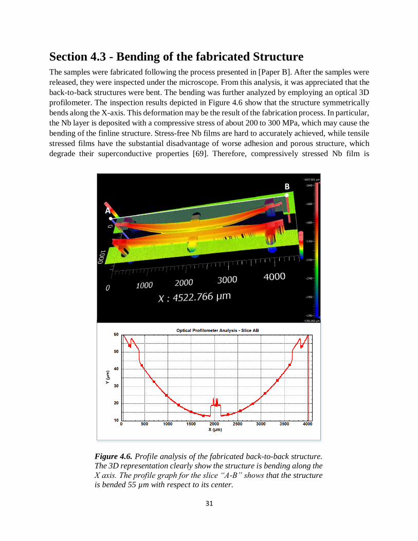
Section 4.3 - Bending of the fabricated Structure .............................................................................................. 31
Section 4.4 - Cryogenic Measurements of Substrateless Finline ......................................................................... 32
Section 4.5 - State of the Art Comparison ......................................................................................................... 35
Chapter 5 - Ongoing Research: Ultrawideband Slotline to Microstrip Transition for 211-375 GHz based on
Marchand Balun ................................................................................................................................................. 37
Section 5.1 - Transition design ......................................................................................................................... 37
Section 5.2 - Back to Back Electromagnetic Simulation .................................................................................... 39
Section 5.3 - Test Chip Design ......................................................................................................................... 40
Section 5.4 - Ongoing Work ............................................................................................................................. 40
Chapter 6 - Conclusion and Future Outlook ..................................................................................................... 42
Appendix I - Simplified equations for third-order Chebyshev Marchand balun calculation. .......................... 44
Appendix II - Fabrication Process of Marchand Balun Test Chips .................................................................. 45
Bibliography .......................................................................................................................................... 47
1
Chapter 1 - Introduction
The human eyes perceive a small fraction of the electromagnetic spectrum that is commonly
referred as visible light. Nevertheless, the electromagnetic spectrum extends far beyond the optical
region, and it is traditionally divided from low to high frequency in: radio waves, microwaves,
THz, infrared, visible light, UV, and X rays, as depicted in Figure 1.1. Among these spectral
regions, the THz range, which falls between 100 GHz (3 mm) and 10 THz (3 0µm), has recently
drawn increasing attention in the scientific community. The interest in this particular frequency
range is motivated by its numerous applications in fundamental and applied science, e.g. bio- and
medical science [2], material science [3], and radio astronomy [4]. Moreover, the continuous
advancement in generation and measurement techniques at this frequency range is taking the THz
wireless communications systems one step closer to reality [5]. These advancements have been
led by the research on radio astronomy instrumentation which has continuously pushed the
technological boundaries and redefined the state of the art technology at THz frequencies [6-8].
For radio astronomy researchers, the study of this section of the electromagnetic spectrum is
especially relevant since half of the luminosity of the Universe, and 98% of the emitted photon
from the Big Bang corresponds to THz radiation [9]. The observation of the cosmos in the THz
region holds the key for answering fundamental questions, ranging from the formation of our Solar
System to the existence of life in other planets [4]. Answering these questions has inspired
worldwide efforts to develop and build radio telescopes to perform high-resolution observations
at millimetre and submillimetre wavelengths. In the last decade, these observations have led to
significant milestones for radio astronomy. For instance, the first picture of a supermassive black
hole was taken by the Event Horizon Telescope (EHT) [10]. The EHT is a virtual interferometric
Figure 1.1. Illustration of the electromagnetic spectrum divisions and frequency ranges.
Reproduced from [1].
2
telescope that spans nearly the diameter of the Earth by combining multiple telescopes located
around the globe, e.g. the Northern Extended Millimeter Array (NOEMA) [11], the Atacama
Pathfinder Experiment (APEX) [12] and the Atacama Large Millimeter/Submillimeter Array
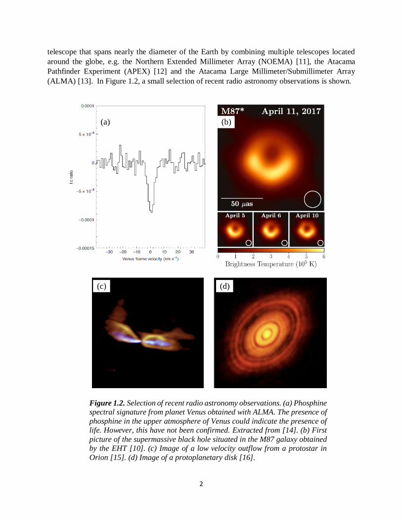
(ALMA) [13]. In Figure 1.2, a small selection of recent radio astronomy observations is shown.
(b)(a)
(c) (d)
Figure 1.2. Selection of recent radio astronomy observations. (a) Phosphine
spectral signature from planet Venus obtained with ALMA. The presence of
phosphine in the upper atmosphere of Venus could indicate the presence of
life. However, this have not been confirmed. Extracted from [14]. (b) First
picture of the supermassive black hole situated in the M87 galaxy obtained
by the EHT [10]. (c) Image of a low velocity outflow from a protostar in
Orion [15]. (d) Image of a protoplanetary disk [16].
3
A large number of radio astronomy observations are performed employing state of the art
heterodyne receivers with high spectral resolution. Although modern THz receivers have already
achieved an outstanding performance [6,22,29], the science goals set for the next decades will
demand remarkable technological development. The recommendations found in technological
roadmaps such as the ALMA roadmap to 2030 [16], and VLBI 20-30: “a scientific roadmap for
the next decade” [81], reflect the needs for the next generation of radio astronomy receivers. In
particular, wider IF and RF bandwidths are of foremost importance for the future of radio
astronomy. To secure a large instantaneous RF bandwidth, the present work proposes a number of
ultra-wideband passive devices for the next generation of THz receivers. Nevertheless, it should
be mentioned that these components are an attractive solution for a diverse range of applications,
such as THz wireless communications [5] and bio- and medical science [2].
Thesis structure
The thesis consists of six chapters, two appendixes, a table of contents and bibliography. Chapter
1 and 2 provide a brief overview of the scientific and technological background behind this thesis.
Chapter 3 details the design of a novel waveguide step twist for the frequency range 140-220 GHz.
Meanwhile, Chapter 4 elaborates on the development of a novel type of finlines, the substrateless
finlines. Moreover, Chapter 4 describes the design and the cryogenic measurements of a
waveguide to substrate transition for the frequency range 211-375 GHz, which allows covering
ALMA band 6 (211-275 GHz), and ALMA band 7 (275-375GHz) simultaneously. In Chapter 5,
the work in progress on slotline to microstrip transitions based on Marchand Baluns is detailed.
Finally, the concluding remarks and future outlook are presented in Chapter 6.
4
(2.1)
Chapter 2 - Scientific and Technological Background
Overview: This chapter provides scientific and technological background for the thesis. In section
2.1, the following fundamental concepts of radio astronomy receivers are explained: detector
types, heterodyne detection fundamentals and the importance of the system noise temperature.
These concepts set the foundations for the devices presented in this thesis, i.e. a compact single
step 90° waveguide twist with a simplified layout, a waveguide to substrate transition based on the
novel substrateless finlines, and a slotline to substrate transition based on Marchand Baluns.
Section 2.2 details the most critical waveguide components for radio astronomy receivers. Among
those, the 90° waveguide twists found in the literature are analyzed. This analysis allows us to
define the motivation and background for the device presented in [Paper A]. Furthermore, Section
2.3 elaborates on the advantages and disadvantages of the existing waveguide to substrate
transitions and the motivations behind the design presented in [Paper B]. Finally, section 2.4
explores the different slotline to microstrip transitions found in the literature and justifies the need
for the ongoing research effort on ultrawideband Marchand Balun transitions.
Section 2.1 - Radio astronomy Detectors
The radio astronomy receivers are intended to detect extremely weak signals that can easily be
outpowered by noise. The noise affecting the receiver might come from external and internal
sources. However, in many cases, the ultimate noise performance of the receiver is limited by the
noise produced in the detector itself. Therefore, the detector noise must be minimized. This
requirement is critical for the receiver performance since the sensitivity of the radiotelescope is
intrinsically related with the noise temperature by the radiometer equation [17]:
𝑆 ∝ 𝑇𝑆𝑌𝑆
√𝜏𝑖𝑛𝑡 𝐵
where S is the sensitivity, i.e. the minimum change in the input signal that the system can detect.
Meanwhile, 𝜏𝑖𝑛𝑡 is the integration time, and B and 𝑇𝑆𝑌𝑆 are the bandwidth and the noise
temperature of the system, respectively. It is essential to mention that 𝑇𝑆𝑌𝑆 is defined for the entire
system and includes the contributions of the receiver, antenna, atmosphere, ground and source.
From equation 2.1, it can be seen that the system noise temperature is linearly related to the
sensitivity. In contrast, the dependence with the integration time is the inverse of the square root.
These relations indicate that reducing the system noise temperature is the most efficient option to
increase the sensitivity.
5
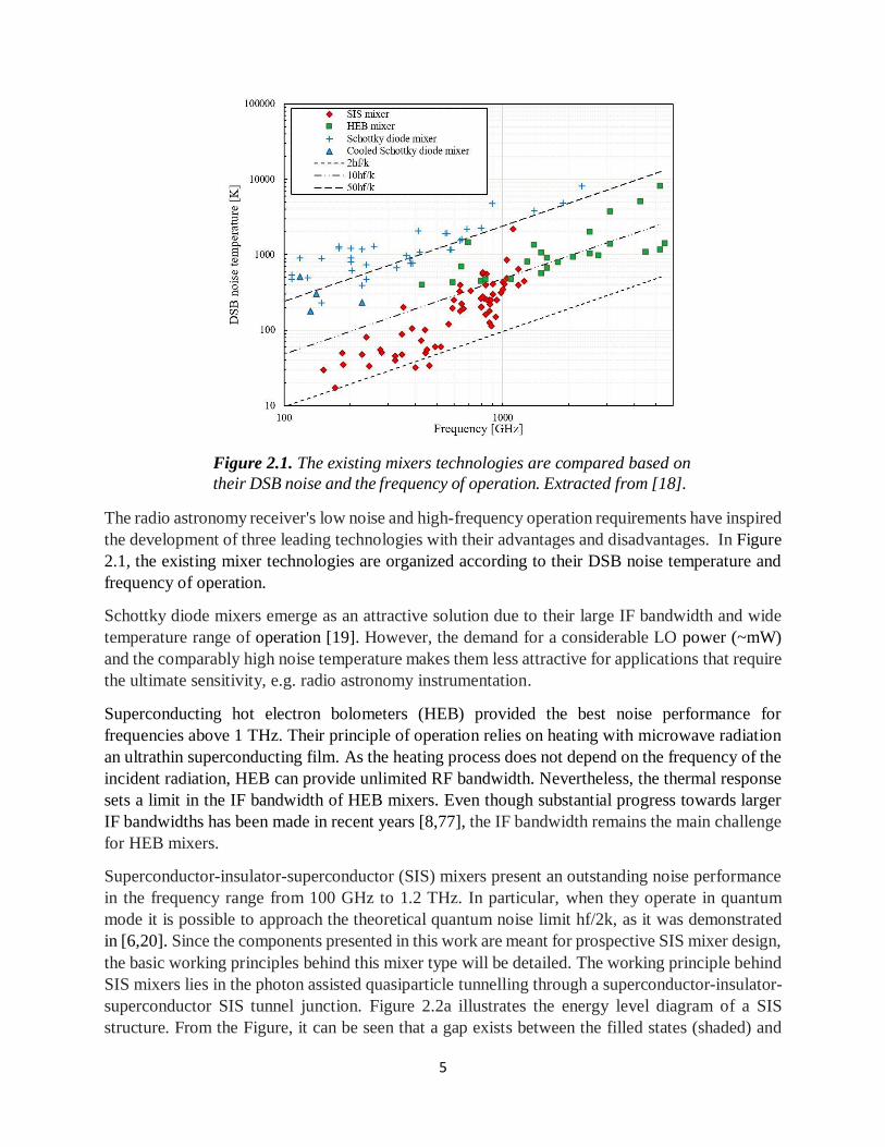
The radio astronomy receiver's low noise and high-frequency operation requirements have inspired
the development of three leading technologies with their advantages and disadvantages. In Figure
2.1, the existing mixer technologies are organized according to their DSB noise temperature and
frequency of operation.
Schottky diode mixers emerge as an attractive solution due to their large IF bandwidth and wide
temperature range of operation [19]. However, the demand for a considerable LO power (~mW)
and the comparably high noise temperature makes them less attractive for applications that require
the ultimate sensitivity, e.g. radio astronomy instrumentation.
Superconducting hot electron bolometers (HEB) provided the best noise performance for
frequencies above 1 THz. Their principle of operation relies on heating with microwave radiation
an ultrathin superconducting film. As the heating process does not depend on the frequency of the
incident radiation, HEB can provide unlimited RF bandwidth. Nevertheless, the thermal response
sets a limit in the IF bandwidth of HEB mixers. Even though substantial progress towards larger
IF bandwidths has been made in recent years [8,77], the IF bandwidth remains the main challenge
for HEB mixers.
Superconductor-insulator-superconductor (SIS) mixers present an outstanding noise performance
in the frequency range from 100 GHz to 1.2 THz. In particular, when they operate in quantum
mode it is possible to approach the theoretical quantum noise limit hf/2k, as it was demonstrated
in [6,20]. Since the components presented in this work are meant for prospective SIS mixer design,
the basic working principles behind this mixer type will be detailed. The working principle behind
SIS mixers lies in the photon assisted quasiparticle tunnelling through a superconductor-insulator-
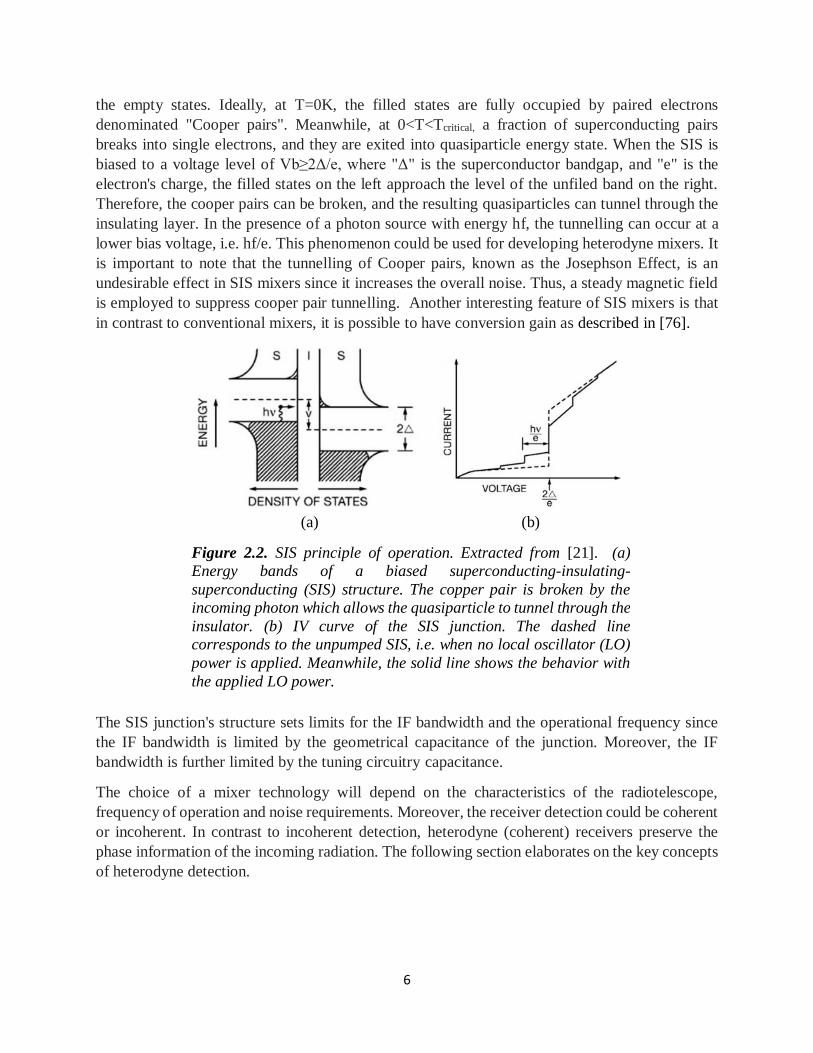
superconductor SIS tunnel junction. Figure 2.2a illustrates the energy level diagram of a SIS
structure. From the Figure, it can be seen that a gap exists between the filled states (shaded) and
Figure 2.1. The existing mixers technologies are compared based on
their DSB noise and the frequency of operation. Extracted from [18].
6
the empty states. Ideally, at T=0K, the filled states are fully occupied by paired electrons
denominated "Cooper pairs". Meanwhile, at 0<T<Tcritical, a fraction of superconducting pairs
breaks into single electrons, and they are exited into quasiparticle energy state. When the SIS is
biased to a voltage level of Vb≥2Δ/e, where "Δ" is the superconductor bandgap, and "e" is the
electron's charge, the filled states on the left approach the level of the unfiled band on the right.
Therefore, the cooper pairs can be broken, and the resulting quasiparticles can tunnel through the
insulating layer. In the presence of a photon source with energy hf, the tunnelling can occur at a
lower bias voltage, i.e. hf/e. This phenomenon could be used for developing heterodyne mixers. It
is important to note that the tunnelling of Cooper pairs, known as the Josephson Effect, is an
undesirable effect in SIS mixers since it increases the overall noise. Thus, a steady magnetic field
is employed to suppress cooper pair tunnelling. Another interesting feature of SIS mixers is that
in contrast to conventional mixers, it is possible to have conversion gain as described in [76].
The SIS junction's structure sets limits for the IF bandwidth and the operational frequency since
the IF bandwidth is limited by the geometrical capacitance of the junction. Moreover, the IF
bandwidth is further limited by the tuning circuitry capacitance.
The choice of a mixer technology will depend on the characteristics of the radiotelescope,
frequency of operation and noise requirements. Moreover, the receiver detection could be coherent
or incoherent. In contrast to incoherent detection, heterodyne (coherent) receivers preserve the
phase information of the incoming radiation. The following section elaborates on the key concepts
of heterodyne detection.
(a) (b)
Figure 2.2. SIS principle of operation. Extracted from [21]. (a)
Energy bands of a biased superconducting-insulating-
superconducting (SIS) structure. The copper pair is broken by the
incoming photon which allows the quasiparticle to tunnel through the
insulator. (b) IV curve of the SIS junction. The dashed line
corresponds to the unpumped SIS, i.e. when no local oscillator (LO)
power is applied. Meanwhile, the solid line shows the behavior with
the applied LO power.
7
(2.2)
(2.3)
(2.4)
(2.5)
(2.6)
Concepts of Heterodyne Detection
A frequency mixer is essentially an analogue multiplication of two signals with different
frequencies denominated Local Oscillator (LO) and Radio Frequency (RF). The LO is generated
in a reference source, while the RF signal presents the information of interest. The mixing between
the LO and the RF produces a signal called Intermediate Frequency (IF) that fully preserves the
phase and amplitude of the RF information. The IF frequency is higher or lower than the RF
depending on whether the process is up-conversion or down-conversion. While up-conversion is
typically employed in transmitters, the down-conversion process is found in receivers1.
The mixer element's nonlinear nature produces a large variety of harmonics and undesired signals
that must be filtered out at the output. The following power series function describes a classical
regime mixer response:
𝐼(𝑡) = 𝑎0 + 𝑎1𝑉(𝑡) + 𝑎2𝑉(𝑡)2 + 𝑎3𝑉(𝑡)3 + ⋯ 𝑎𝑛𝑉(𝑡)𝑛
Where 𝐼(𝑡) is the time dependent current at the mixer output. When LO and RF are applied , 𝑉(𝑡)
is defined as:
𝑉(𝑡) = 𝑉𝐿𝑂 cos(2𝜋𝑓𝐿𝑂𝑡) + 𝑉𝑅𝐹 cos(2𝜋𝑓𝑅𝐹 𝑡)
Therefore, the mixer will generate at its output a large number of frequency components based on
the addition, subtraction and multiplication of the original 𝑓𝐿𝑂 and 𝑓𝑅𝐹 . However, the frequency
components that are interesting for the conversion process are:
𝐼(𝑡) ∝ K cos(2𝜋𝑓𝐿𝑂𝑡) cos(2𝜋𝑓𝑅𝐹𝑡)
𝐼(𝑡) ∝K
2[cos 2𝜋(𝑓𝑅𝐹 + 𝑓𝐿𝑂)𝑡 + cos 2𝜋(𝑓𝑅𝐹 − 𝑓𝐿𝑂)𝑡]
𝑓𝐼𝐹 = 𝑓𝑅𝐹 ± 𝑓𝐿𝑂
The intermediate frequency can be filtered from the rest of the undesirable frequency components.
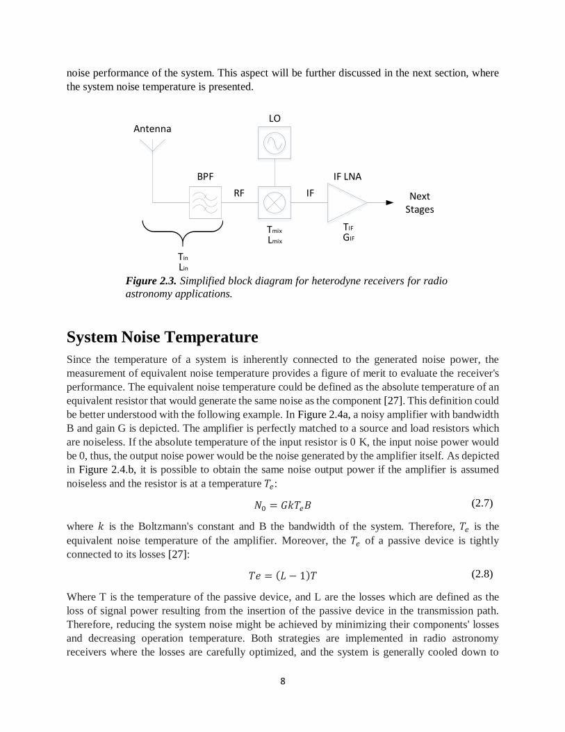
Many radio astronomy receivers make use of the down-conversion process to detect and process
the high frequency signals that come from celestial bodies, e.g. [6,22,23,29]. In Figure 2.3, the
simplified block diagram for a heterodyne radio astronomy receiver is shown. The bandpass
response is provided by the interconnection components located between the antenna and the
mixing element, i.e. horn, orthomode transducer (OMT), and waveguide to substrate transition.
It is essential to note that radio astronomy receivers operating below ~100 GHz incorporate a RF
low noise amplifier (LNA) as the first stage, e.g. ALMA band 2 receiver [24]. Even though LNA
technology is progressing towards frequencies above ~100 GHz, e.g. [25,26], RF LNAs are not
employed in high frequency receivers since the noise of such devices so far is too large compared
to the extremely sensitive SIS mixer. Therefore, the inclusion of an RF LNA would deteriorate the
1 Part of this section follows the book by David Pozar “Microwave Engineering”
8
(2.7)
(2.8)
noise performance of the system. This aspect will be further discussed in the next section, where
the system noise temperature is presented.
System Noise Temperature
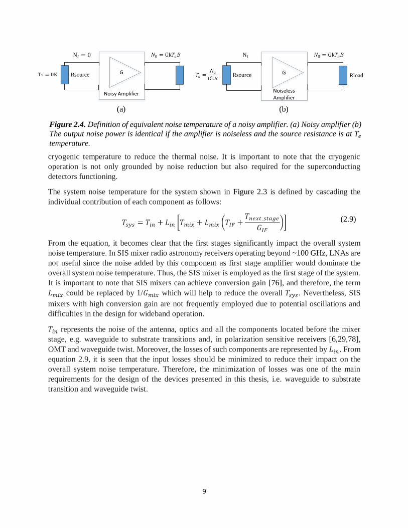
Since the temperature of a system is inherently connected to the generated noise power, the
measurement of equivalent noise temperature provides a figure of merit to evaluate the receiver's
performance. The equivalent noise temperature could be defined as the absolute temperature of an
equivalent resistor that would generate the same noise as the component [27]. This definition could
be better understood with the following example. In Figure 2.4a, a noisy amplifier with bandwidth
B and gain G is depicted. The amplifier is perfectly matched to a source and load resistors which
are noiseless. If the absolute temperature of the input resistor is 0 K, the input noise power would
be 0, thus, the output noise power would be the noise generated by the amplifier itself. As depicted
in Figure 2.4.b, it is possible to obtain the same noise output power if the amplifier is assumed
noiseless and the resistor is at a temperature 𝑇𝑒:
𝑁0 = 𝐺𝑘𝑇𝑒𝐵
where 𝑘 is the Boltzmann's constant and B the bandwidth of the system. Therefore, 𝑇𝑒 is the
equivalent noise temperature of the amplifier. Moreover, the 𝑇𝑒 of a passive device is tightly
connected to its losses [27]:
𝑇𝑒 = (𝐿 − 1)𝑇
Where T is the temperature of the passive device, and L are the losses which are defined as the
loss of signal power resulting from the insertion of the passive device in the transmission path.
Therefore, reducing the system noise might be achieved by minimizing their components' losses
and decreasing operation temperature. Both strategies are implemented in radio astronomy
receivers where the losses are carefully optimized, and the system is generally cooled down to
LO
RF
BPF
Antenna
IF
IF LNA
Tin
Lin
Tmix
Lmix
Next Stages
TIF
GIF
Figure 2.3. Simplified block diagram for heterodyne receivers for radio
astronomy applications.
9
(2.9)
cryogenic temperature to reduce the thermal noise. It is important to note that the cryogenic
operation is not only grounded by noise reduction but also required for the superconducting
detectors functioning.
The system noise temperature for the system shown in Figure 2.3 is defined by cascading the
individual contribution of each component as follows:
𝑇𝑠𝑦𝑠 = 𝑇𝑖𝑛 + 𝐿𝑖𝑛 [𝑇𝑚𝑖𝑥 + 𝐿𝑚𝑖𝑥 (𝑇𝐼𝐹 +𝑇𝑛𝑒𝑥𝑡_𝑠𝑡𝑎𝑔𝑒
𝐺𝐼𝐹)]
From the equation, it becomes clear that the first stages significantly impact the overall system
noise temperature. In SIS mixer radio astronomy receivers operating beyond ~100 GHz, LNAs are
not useful since the noise added by this component as first stage amplifier would dominate the
overall system noise temperature. Thus, the SIS mixer is employed as the first stage of the system.
It is important to note that SIS mixers can achieve conversion gain [76], and therefore, the term
𝐿𝑚𝑖𝑥 could be replaced by 1/𝐺𝑚𝑖𝑥 which will help to reduce the overall 𝑇𝑠𝑦𝑠. Nevertheless, SIS
mixers with high conversion gain are not frequently employed due to potential oscillations and
difficulties in the design for wideband operation.
𝑇𝑖𝑛 represents the noise of the antenna, optics and all the components located before the mixer
stage, e.g. waveguide to substrate transitions and, in polarization sensitive receivers [6,29,78],
OMT and waveguide twist. Moreover, the losses of such components are represented by 𝐿𝑖𝑛. From
equation 2.9, it is seen that the input losses should be minimized to reduce their impact on the
overall system noise temperature. Therefore, the minimization of losses was one of the main
requirements for the design of the devices presented in this thesis, i.e. waveguide to substrate
transition and waveguide twist.
G
Noisy Amplifier
Rsource
G
Noiseless Amplifier
Rsource Rload
(a) (b)
Figure 2.4. Definition of equivalent noise temperature of a noisy amplifier. (a) Noisy amplifier (b)
The output noise power is identical if the amplifier is noiseless and the source resistance is at 𝑇𝑒
temperature.
10
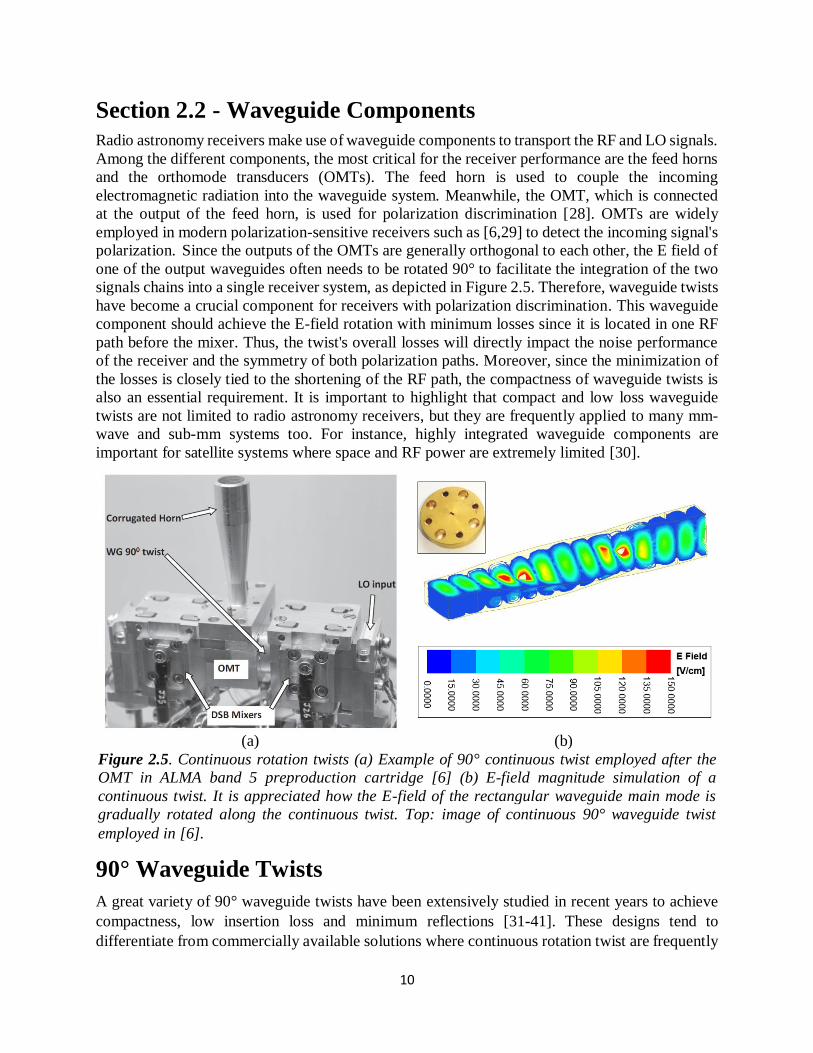
Section 2.2 - Waveguide Components
Radio astronomy receivers make use of waveguide components to transport the RF and LO signals.
Among the different components, the most critical for the receiver performance are the feed horns
and the orthomode transducers (OMTs). The feed horn is used to couple the incoming
electromagnetic radiation into the waveguide system. Meanwhile, the OMT, which is connected
at the output of the feed horn, is used for polarization discrimination [28]. OMTs are widely
employed in modern polarization-sensitive receivers such as [6,29] to detect the incoming signal's
polarization. Since the outputs of the OMTs are generally orthogonal to each other, the E field of
one of the output waveguides often needs to be rotated 90° to facilitate the integration of the two
signals chains into a single receiver system, as depicted in Figure 2.5. Therefore, waveguide twists
have become a crucial component for receivers with polarization discrimination. This waveguide
component should achieve the E-field rotation with minimum losses since it is located in one RF
path before the mixer. Thus, the twist's overall losses will directly impact the noise performance
of the receiver and the symmetry of both polarization paths. Moreover, since the minimization of
the losses is closely tied to the shortening of the RF path, the compactness of waveguide twists is
also an essential requirement. It is important to highlight that compact and low loss waveguide
twists are not limited to radio astronomy receivers, but they are frequently applied to many mm-
wave and sub-mm systems too. For instance, highly integrated waveguide components are
important for satellite systems where space and RF power are extremely limited [30].
90° Waveguide Twists
A great variety of 90° waveguide twists have been extensively studied in recent years to achieve
compactness, low insertion loss and minimum reflections [31-41]. These designs tend to
differentiate from commercially available solutions where continuous rotation twist are frequently
(a) (b)
Figure 2.5. Continuous rotation twists (a) Example of 90° continuous twist employed after the
OMT in ALMA band 5 preproduction cartridge [6] (b) E-field magnitude simulation of a
continuous twist. It is appreciated how the E-field of the rectangular waveguide main mode is
gradually rotated along the continuous twist. Top: image of continuous 90° waveguide twist
employed in [6].
11
employed. Continuous twist relies on the gradual rotation of the E-field inside a twisted rectangular
waveguide, as shown by Figure 2.5b. The gradual rotation guarantees broadband operation with
minimum reflections. However, continuous twists require a length of several guided wavelengths,
which makes them incompatible with highly integrated waveguide systems. Moreover, the
electroforming process employed for its fabrication is costly and takes a significant amount of
time.
An alternative solution was explored in the designs presented in [32-34], which are based on multi-
step twists. These twists are formed by a series of waveguide sections that are gradually rotated
until the full E-field rotation is achieved. Although this solution is less bulky than continuous twist,
its fabrication is rather complicated. Furthermore, the overall performance of the multi-step twists
depends on the fabrication and mounting tolerances of each section. Therefore, these twists are
especially challenging to implement at higher frequencies where mounting tolerances are more
critical.
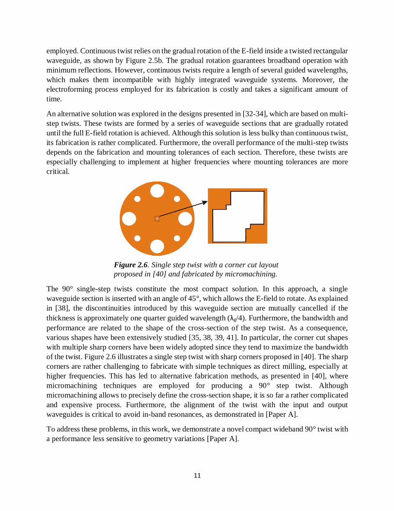
The 90° single-step twists constitute the most compact solution. In this approach, a single
waveguide section is inserted with an angle of 45°, which allows the E-field to rotate. As explained
in [38], the discontinuities introduced by this waveguide section are mutually cancelled if the
thickness is approximately one quarter guided wavelength (λg/4). Furthermore, the bandwidth and
performance are related to the shape of the cross-section of the step twist. As a consequence,
various shapes have been extensively studied [35, 38, 39, 41]. In particular, the corner cut shapes
with multiple sharp corners have been widely adopted since they tend to maximize the bandwidth
of the twist. Figure 2.6 illustrates a single step twist with sharp corners proposed in [40]. The sharp
corners are rather challenging to fabricate with simple techniques as direct milling, especially at
higher frequencies. This has led to alternative fabrication methods, as presented in [40], where
micromachining techniques are employed for producing a 90° step twist. Although
micromachining allows to precisely define the cross-section shape, it is so far a rather complicated
and expensive process. Furthermore, the alignment of the twist with the input and output
waveguides is critical to avoid in-band resonances, as demonstrated in [Paper A].
To address these problems, in this work, we demonstrate a novel compact wideband 90° twist with
a performance less sensitive to geometry variations [Paper A].
Figure 2.6. Single step twist with a corner cut layout
proposed in [40] and fabricated by micromachining.
12
Section 2.3 - Waveguide to Substrate Transitions
Thin-film technology is the main pillar for mixer fabrication in radio astronomy receivers, thus,
waveguide to substrate transitions play a crucial role in the receiver performance. The main
requirements for the waveguide to substrate transitions are a low insertion loss accompanied by
proper impedance matching. In addition, a simple mounting process and the associated mounting
tolerances are also essential requirements.
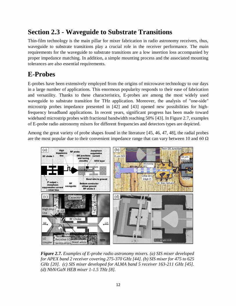
E-Probes
E-probes have been extensively employed from the origins of microwave technology to our days
in a large number of applications. This enormous popularity responds to their ease of fabrication
and versatility. Thanks to these characteristics, E-probes are among the most widely used
waveguide to substrate transition for THz application. Moreover, the analysis of "one-side"
microstrip probes impedance presented in [42] and [43] opened new possibilities for high-
frequency broadband applications. In recent years, significant progress has been made toward
wideband microstrip probes with fractional bandwidth reaching 50% [43]. In Figure 2.7, examples
of E-probe radio astronomy mixers for different frequencies and detectors types are depicted.
Among the great variety of probe shapes found in the literature [45, 46, 47, 48], the radial probes
are the most popular due to their convenient impedance range that can vary between 10 and 60 Ω
(a) (b)
(c) (d)
Figure 2.7. Examples of E-probe radio astronomy mixers. (a) SIS mixer developed
for APEX band 2 receiver covering 275-370 GHz [44]. (b) SIS mixer for 475 to 625
GHz [20]. (c) SIS mixer developed for ALMA band 5 receiver 163-211 GHz [45].
(d) NbN/GaN HEB mixer 1-1.5 THz [8].
13
depending on the substrate and radius [43]. The pure real impedances can only be obtained by
tuning out the impedance imaginary part. This cancellation is strongly dependent on the probe's
position with respect to a waveguide backshort. The backshort is generally situated at λg/4 and
constitutes the main limitation for the maximum bandwidth of E-probes. Thus, the mounting
accuracy and machining tolerances become rather critical for the performance, especially at mm-
wave and THz frequencies. In [43], a capacitive step is introduced in the input waveguide to
increase the fractional bandwidth. Although this approach dramatically improves the probe's
bandwidth, it does not solve the tolerance issues associated with E probes. Therefore, it becomes
clear that there is a need for an alternative waveguide to substrate transition for the next generation
of radio astronomy receivers.
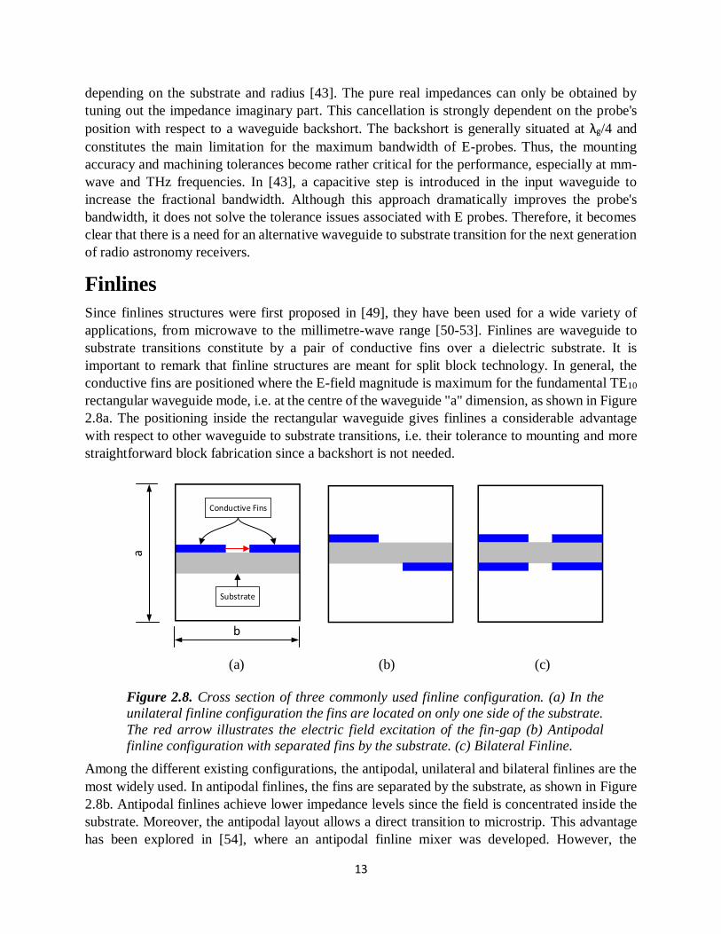
Finlines
Since finlines structures were first proposed in [49], they have been used for a wide variety of
applications, from microwave to the millimetre-wave range [50-53]. Finlines are waveguide to
substrate transitions constitute by a pair of conductive fins over a dielectric substrate. It is
important to remark that finline structures are meant for split block technology. In general, the
conductive fins are positioned where the E-field magnitude is maximum for the fundamental TE10
rectangular waveguide mode, i.e. at the centre of the waveguide "a" dimension, as shown in Figure
2.8a. The positioning inside the rectangular waveguide gives finlines a considerable advantage
with respect to other waveguide to substrate transitions, i.e. their tolerance to mounting and more
straightforward block fabrication since a backshort is not needed.
Among the different existing configurations, the antipodal, unilateral and bilateral finlines are the
most widely used. In antipodal finlines, the fins are separated by the substrate, as shown in Figure
2.8b. Antipodal finlines achieve lower impedance levels since the field is concentrated inside the
substrate. Moreover, the antipodal layout allows a direct transition to microstrip. This advantage
has been explored in [54], where an antipodal finline mixer was developed. However, the
Substrate
Conductive Fins
b
a
(a) (b) (c)
Figure 2.8. Cross section of three commonly used finline configuration. (a) In the
unilateral finline configuration the fins are located on only one side of the substrate.
The red arrow illustrates the electric field excitation of the fin-gap (b) Antipodal
finline configuration with separated fins by the substrate. (c) Bilateral Finline.

14
performance of the antipodal configurations is sensitive to the alignment between the fins,
especially at high frequencies where a few µm wide fin-gap is frequently employed. This problem
is shared with the bilateral finline configuration since it presents a pair of fins on both sides of the
dielectric slab, as depicted in Figure 2.8c. Furthermore, the bilateral arrangement generally
presents significant losses due to higher field concentration inside the dielectric.
The unilateral layout is the simplest and probably the best suited for high-frequency applications
since both metallizations are located on the same side of the dielectric slab, as illustrated by Figure
2.8a. This configuration eliminates the problems related to the fins' alignment but increases the
overall impedance of the line since a large part of the electromagnetic field propagates outside the
dielectric. The unilateral configuration has been applied for mixer design in [51]. In these designs,
different techniques were employed to mitigate the main problem associated with finlines, i.e. the
impedance matching between the waveguide and the substrate. The poor impedance matching
degrades the performance of the transition and limits its operating bandwidth. In Figure 2.9, a
(a)
(b)
Figure 2.9. Examples of unilateral finline 600-700 GHz radio astronomy mixers.
Extracted from [55]. (a) SIS mixer fabricated over 60 µm quartz. The finline
transition make use of a triangular notch in the quartz substrate to improve
matching. In addition, serration chokes are employed to guard against the
propagation of substrate mode. (b) SIS mixer fabricated over 15 µm Si substrate.
Note the multi-stage silicon matching notch.
15
variety of solutions for improving the matching are presented. These solutions are based on
impedance transformers patterned on the substrate aiming to gradually load the waveguide and
minimize the mismatch. Although these techniques partially solved the matching problem, they
extend the substrate inside the waveguide, which increase the dielectric losses of the transition. An
alternative solution is explored in this thesis [Paper B], where a new type of finline is presented,
the Substrateless finline. In this finline configuration, the substrate confined by the fins is removed
to improve the matching and reduce the dielectric losses.
Section 2.4 - Slotline to Microstrip transitions
Thin-film superconducting microstrips are fully compatible with the fabrication of the trilayer SIS
structure. Furthermore, thin-film microstrips can reach impedances below 10 Ω, which is
especially suitable for the SIS RF impedance matching circuit. Consequently, most modern SIS
mixers rely on thin-film microstrip lines for on-substrate interconnections [45], [79]. On the other
hand, finline structures can be easily coupled to slotlines as the main electromagnetic propagation
mode is essentially identical. Nevertheless, fabricating slotlines with small characteristic
impedance is rather challenging. Therefore, finline mixers usually employ an additional transition
step from slotline to microstrip.
The main requirements for slotline to microstrip transitions are low insertion loss, high return loss,
and chip area minimization. These requirements are challenging to accomplish due to the inherent
impedance difference between slotlines and microstrips. While 40 Ω slotlines can be fabricated
with thin-film technology, lower impedance values are non-practical as the slot dimension
decrease to the µm range and below. On the other hand, it is rather difficult to achieved impedance
values higher than 20 Ω with thin-film microstrips, where the dielectric layer thickness is
comparable to the strip thickness. Therefore, the matching between slotlines and thin-film
microstrip is highly complex. Through the years, a large number of different solutions have been
proposed [55-59].
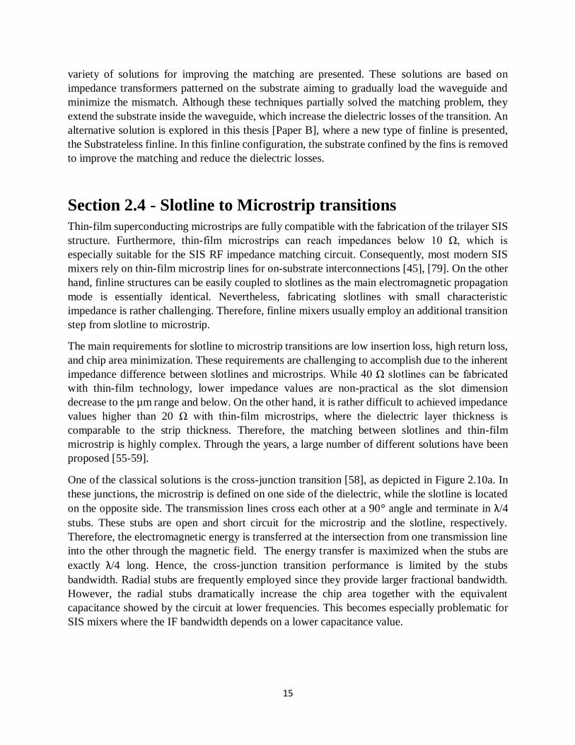
One of the classical solutions is the cross-junction transition [58], as depicted in Figure 2.10a. In
these junctions, the microstrip is defined on one side of the dielectric, while the slotline is located
on the opposite side. The transmission lines cross each other at a 90° angle and terminate in λ/4
stubs. These stubs are open and short circuit for the microstrip and the slotline, respectively.
Therefore, the electromagnetic energy is transferred at the intersection from one transmission line
into the other through the magnetic field. The energy transfer is maximized when the stubs are
exactly λ/4 long. Hence, the cross-junction transition performance is limited by the stubs
bandwidth. Radial stubs are frequently employed since they provide larger fractional bandwidth.
However, the radial stubs dramatically increase the chip area together with the equivalent
capacitance showed by the circuit at lower frequencies. This becomes especially problematic for
SIS mixers where the IF bandwidth depends on a lower capacitance value.
16
Z1
Z2
Zo
M
Z3 ZoS
Microstrip
Slotline
Slotline
Microstrip
Microstrip
Short
Microstrip
Open
Slotline
Short
Slotline
Open
Microstrip
Slotline
CPW
Slotline
Air BridgeSlotline
Stub
Microstrip
StubCPW StubSlotline
Stub
Conductor 1
Conductor 2
Substrate
Conductor Via
(a)
(b)
(c)
(d)
Figure 2.10. Slotline to microstrip transitions. It is important to note that the
dielectric layer located between the conductors is not shown in the images for
clarity. (a) Cross-junction transition. (b) Indirect transition with CPW. (c)
Double Y balun transition (d) Marchand balun transition.

17
Double Y baluns emerge as an alternative solution to cross-junction transitions [59], as displayed
in Figure 2.10c. The double Y balun employs short and opens terminations for both microstrip and
slotlines to optimize energy transfer and improve the overall bandwidth of the transition.
Nonetheless, the slotline open termination significantly increases the area on the chip, and it is a
potential source of resonances due to energy radiation. Furthermore, the realization of the
microstrip short makes the design and fabrication rather complex.
The inherent impedance difference of microstrips and slotlines could be overcome with indirect
transitions, where an auxiliary transmission line is employed to facilitate the matching [55].
Among the different auxiliary lines, coplanar waveguides (CPW) are the most popular solution
due to the wide range of impedances and field compatibility with slotline and microstrip, as
illustrated by Figure 2.10b. Indirect transitions with CPW enhance the bandwidth of microstrip to
slotline transitions. Nevertheless, the fabrication of such transition is rather complex due to the
extra transition steps and the need for an air bridge to suppress parasitic CPW modes.
The Marchand balun transition arises as a promising solution due to its compactness and design
flexibility [56]. The Marchand balun structures resemble the cross-junction transition. However,
its bandwidth does not rely on single λ/4 stubs, but it combines different impedances to synthesize
a particular response. For instance, a third-order Chebyshev passband response could be
synthesized as depicted in Figure 2.10d. Furthermore, since this balun does not employ radial or
circular stubs, the transition is highly compact. These characteristics make Marchand baluns an
attractive solution for broadband low-loss microstrip to slotline transitions. In this work, the
ongoing research towards a Marchand balun transition designed for future SIS mixer design and
integration with substrateless finlines is presented in Chapter 5.

18
Chapter 3 - Wideband 90° Waveguide Twist with
Simplified Layout for 140-220 GHz
In [Paper A], a novel compact wideband 90° twist was presented with a performance less sensitive
to geometry variations than the existing corner cut designs, e.g. [35, 38, 39]. The higher geometric
tolerance of the design allowed simple fabrication techniques as direct milling without
compromising the overall bandwidth and the performance. The design layout presented in Figure
4.1 was intended for the 140-220 GHz band.
Section 4.1 - Simulation of electromagnetic twist modes
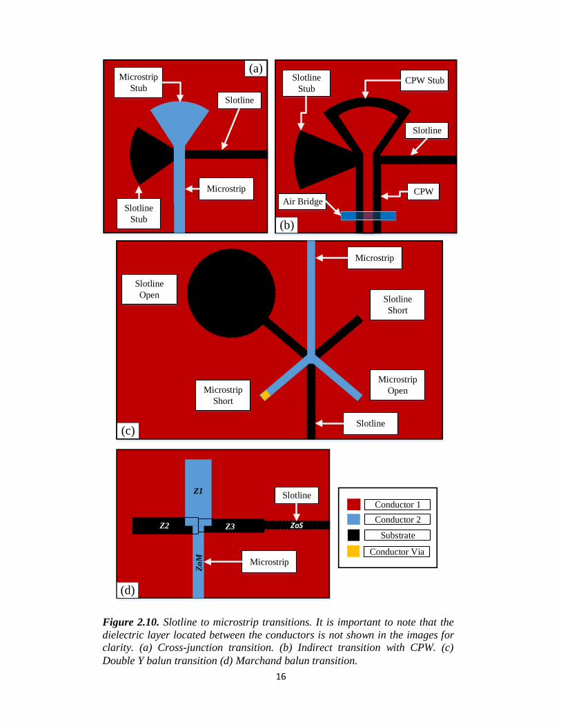
The field rotation process can be better explained if the modes inside the twist cavity are studied.
Figure 3.2 illustrates the electrical field distribution of the first, second and third modes of the twist
cavity. As can be seen, the modes resemble TE10, TE11, and the antisymmetric TE10 modes in a
rectangular waveguide, respectively. However, it is essential to highlight that the twist's second
and third modes are evanescent for the input/output rectangular waveguides connected at port 1
and 2, i.e., they propagate only inside the twist cavity.
To further investigate the propagation modes of the twist, a series of simulations were performed.
Figure 3.3 shows the simulated magnitude of S12 for two configurations: I) the twist as a
standalone component and II) the twist connected to a standard rectangular waveguide in only one
of its ports, as shown in the insert in Figure 3.3. In both configurations, the first three modes were
simulated. For the first configuration, the cut-off frequencies were found to be 120 GHz, 211 GHz
and 223 GHz. Note that the main mode for the standalone twist was not plotted since it propagates
in the whole frequency band and may reduce the graph's clarity.
PORT 1
PORT 2
(a) (b)
Figure 3.1. Waveguide twist presented in [Paper A]. (a) Waveguide twist layout. (b) Cross
Section view and waveguide ports. Dimensions for WR-5.1 Band: R= 460µm, A= 600 µm, B=
500 µm and R2= 100 µm. The thickness of the step twist is 660 µm.
19
When the first configuration is compared with the second, a series of interesting conclusions can
be drawn. In the first place, the second mode's cut off frequency is influenced by the rectangular
waveguide connected to the twist. In contrast, the third mode cut off remains fixed, but a resonance
appears at the same frequency, i.e., 223 GHz. This resonance is "mirrored" at the main mode, as
seen in Figure 3.3. Therefore, the third mode will play a significant role in limiting the operational
PORT 2
PORT 1
(a) (b) (c)
Figure 3.2. Electrical field distribution comparison between Twist
modes and standard rectangular waveguide WR 5.1. Twist modes: (a)
Dominant Mode – Cut off Frequency 120 GHz. (b) Second Mode - Cut
off Frequency 211 GHz.(c) Third Mode – Cut off Frequency 223 GHz.
Figure 3.3. Propagation of the second and third mode for the
standalone twist cavity, and the twist cavity connected to a rectangular
waveguide. The third mode will introduce a resonance in the response.
20
bandwidth of the waveguide twist. A second conclusion can be formulated by analyzing the mode
relations in the twist and rectangular waveguide. When the first mode of the twist cavity is excited
on the input port, the TE10 mode is observed at the rectangular waveguide output. This relation
proves its role in the field rotation process.
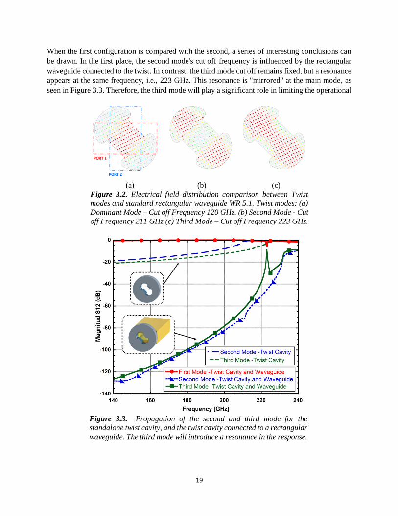
Simulated performance
The operational bandwidth was maximized by carefully positioning the third mode resonance
outside the frequency of operation. The simulation results are illustrated in Figure 3.4.
The twist was simulated with the full-wave 3-D simulator Ansys HFSS [64]. The simulation shows
a return loss better than -20 dB over most of the operation band, which implies a 44% fractional
bandwidth. In addition, the insertion loss is predicted to be below 0.3 dB for the whole frequency
range.
Figure 3.4. Simulated Performance for the desing twist presented in [Paper A]. The
magnitude E-field colour representation shows the field rotation process.
21
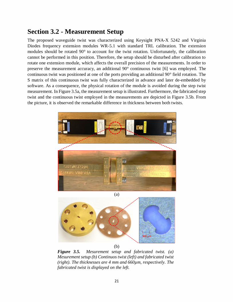
Section 3.2 - Measurement Setup
The proposed waveguide twist was characterized using Keysight PNA-X 5242 and Virginia
Diodes frequency extension modules WR-5.1 with standard TRL calibration. The extension
modules should be rotated 90° to account for the twist rotation. Unfortunately, the calibration
cannot be performed in this position. Therefore, the setup should be disturbed after calibration to
rotate one extension module, which affects the overall precision of the measurements. In order to
preserve the measurement accuracy, an additional 90° continuous twist [6] was employed. The
continuous twist was positioned at one of the ports providing an additional 90° field rotation. The
S matrix of this continuous twist was fully characterized in advance and later de-embedded by
software. As a consequence, the physical rotation of the module is avoided during the step twist
measurement. In Figure 3.5a, the measurement setup is illustrated. Furthermore, the fabricated step
twist and the continuous twist employed in the measurements are depicted in Figure 3.5b. From
the picture, it is observed the remarkable difference in thickness between both twists.
(a)
60
5 µ
m
300 µm
(b)
Figure 3.5. Mesurement setup and fabricated twist. (a)
Mesurement setup (b) Continuos twist (left) and fabricated twist
(right). The thicknesses are 4 mm and 660µm, respectively. The
fabricated twist is displayed on the left.
22
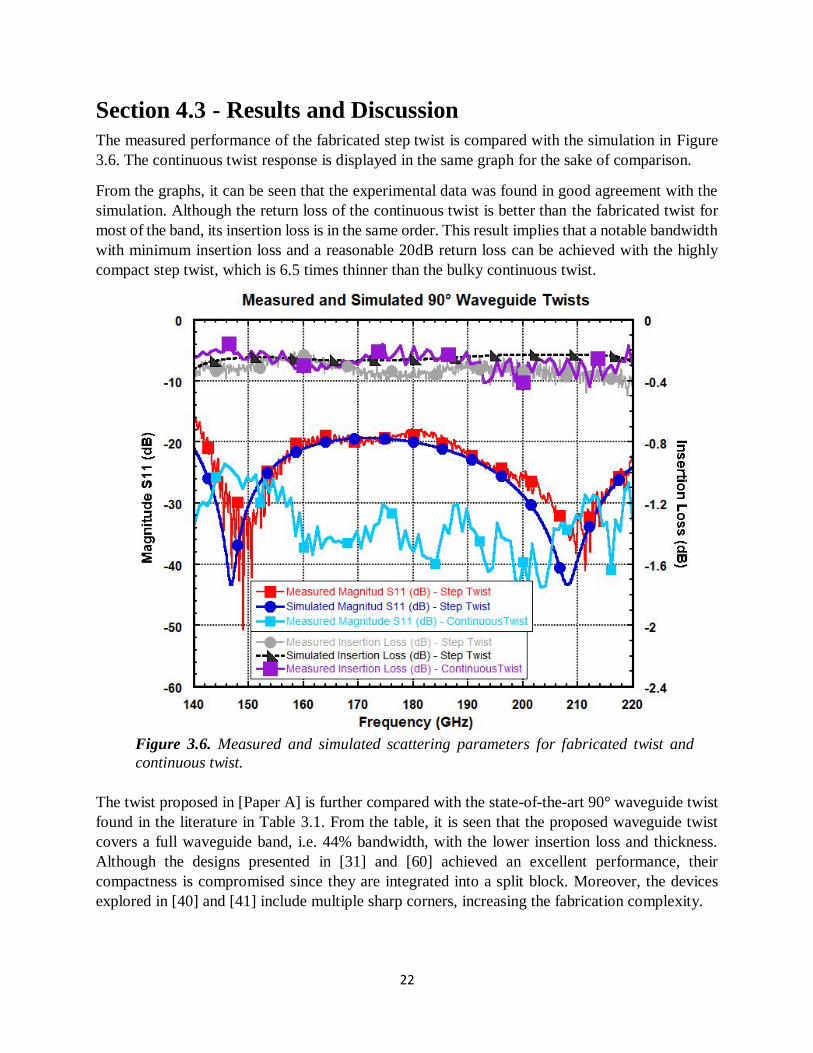
Section 4.3 - Results and Discussion
The measured performance of the fabricated step twist is compared with the simulation in Figure
3.6. The continuous twist response is displayed in the same graph for the sake of comparison.
From the graphs, it can be seen that the experimental data was found in good agreement with the
simulation. Although the return loss of the continuous twist is better than the fabricated twist for
most of the band, its insertion loss is in the same order. This result implies that a notable bandwidth
with minimum insertion loss and a reasonable 20dB return loss can be achieved with the highly
compact step twist, which is 6.5 times thinner than the bulky continuous twist.
The twist proposed in [Paper A] is further compared with the state-of-the-art 90° waveguide twist
found in the literature in Table 3.1. From the table, it is seen that the proposed waveguide twist
covers a full waveguide band, i.e. 44% bandwidth, with the lower insertion loss and thickness.
Although the designs presented in [31] and [60] achieved an excellent performance, their
compactness is compromised since they are integrated into a split block. Moreover, the devices
explored in [40] and [41] include multiple sharp corners, increasing the fabrication complexity.
Figure 3.6. Measured and simulated scattering parameters for fabricated twist and
continuous twist.

23
IL: Insertion Loss RL: Reflection Loss 𝝀𝑮: guided wavelength.
RefFrequency
[GHz]
Franctional
BandwidthLength [λg]
IL
[dB]
RL
[dB]Geometry Comment
[6] 140-220 44% 1.8 ⁓0.2 30
Continuous Twist
-Fabricated by
Electroforming.
220-320 37% ˃ 4 0.5 ⁓20
500-700 33% Not reported 2.5 20
[33] 75-110 37% 1.12 0.11 25
Multistep Twist
-Fabricated by
direct milling.
[40] 600-750 22% 0.43 0.5 20
Single step Twist
-Fabricated by
micromachining.
[60] 220-330 40% 8.75 0.6 20
Single step Twist
integrated in split
block - Fabricated
by direct milling.
[31] 220-330 40% 18.14 1 25
Multistep Twist
integrated in split
block - Fabricated
by direct milling.
[Paper A] 140-220 44% 0.3 0.4 ⁓20
Single step Twist
-Fabricated by
direct milling.
Table 3.1 - State of the art comparison of 90° Twists
[41]
Continuous Twist
-Fabricated by
direct milling.

24
From the comparison, it becomes clear that the twist proposed in [Paper A] combines a highly
compact design with a remarkable fractional bandwidth and minimum losses. Moreover, the
absence of sharp corners makes the design suitable for standard milling techniques at least up to
220 GHz. Furthermore, the presented design can be easily scaled down to lower frequency,
extending its applicability to a large number of broadband highly integrated waveguide systems.

25
Chapter 4 - The Substrateless Finlines
The substrateless finline is a novel type of unilateral finline where the substrate between the
conductive fins has been completely removed, as shown in Figure 4.1. Meanwhile, the substrate
under the fins is preserved. The substrate removal addresses two fundamental problems of
waveguides to finlines transitions, i.e. the dielectric losses on the substrate and the impedance
matching over large bandwidths. As discussed in Section 2.3, the impedance match of finline
transitions is usually compromised by the discontinuity between the dielectric slab and the
waveguide. In contrast, the substrateless finline introduces the dielectric slab gradually, which
dramatically improves the matching with the waveguide and the resulting bandwidth of the
transition. Therefore, substrateless finlines could potentially be employed for wideband designs.
In this work, the development of this novel transmission line was intended for wideband cryogenic
mixer design in the frequency range 211-375 GHz.
Figure 4.2 depicts the E-field distribution in a waveguide to substrateless finline transition. It is
seen how the fundamental waveguide mode TE10 is transformed into a finline mode. Since this
field distribution is identical to the slotline mode, the electromagnetic energy can be naturally
coupled later to a slotline.
Waveguide
Substrate
Fins
Removed Substrate
Figure 4.1. Substrateless Finline waveguide to substrate transition. Note that the
substrate enclosed by the conducting fins has been removed. The red arrow
indicates the E-field orientation in the waveguide input.

26
Section 4.1 - Design of Substrateless Finlines
The taper shape defines the performance of waveguide to finline transitions. In the last decades,
several methods for finline taper design have been proposed and tested [61-63]. Nevertheless, these
methods have been specially formulated for regular finlines where the substrate between the fins
has not been removed. Therefore, in this work, a new method for designing substrateless finline
tapers was investigated and presented in [Paper B].
An arbitrary finline taper profile can be generated if the characteristic impedance and the guided
wavelength functions are known. The relations between impedance, guided wavelength and fin-
gap size can be explored with the help of the full-wave 3-D simulator Ansys HFSS [64].
Employing a single section of substrateless finline, the main parameters of the substrateless finline
can be investigated and mapped for different fin-gap. Afterwards, the mapped values can be used
to create polynomial approximations that relate the different parameters. However, it should be
noted that the approximations produced with this method are only applicable to the conditions
established in the simulation. In particular, it is crucial to define the dielectric slab characteristics,
i.e. dielectric constant and thickness, since the substrateless finline impedance depends on these
values. In this work, float-zone silicon of 30 µm thickness was chosen as the finline substrate. The
selection of float-zone silicon was motivated by its low loss at cryogenic temperatures. Moreover,
the maturity of the Si etching technology allows removing of the substrate easily. Regarding the
thickness of the Si substrate, 30 µm was selected to prevent substrate modes from propagating in
the structure [65]. Moreover, the silicon substrate was enclosed by an 800 µm x 400 µm
waveguide. This waveguide size completely covers the frequency range which was targeted in the
design, i.e. 211-375 GHz.
Once the substrate and frequency range were selected, substrateless finline for fin-gaps ranging
from 4 to 400 µm were simulated. Therefore, the impedance and guide lambda vs. fin-gap was
obtained. This data was employed to develop polynomial approximation functions, which can be
used for multi-step transformer design, as discussed in the next section. A similar procedure was
performed for characterizing superconducting slotlines.
Waveguide
Waveguide Input
Substrate
Figure 4.2. E-field magnitude distribution in a waveguide to substrateless
finline transition. The waveguide input is excited with TE10 mode.
27
Section 4.2 - Waveguide to Substrate transition employing
Substrateless Finlines
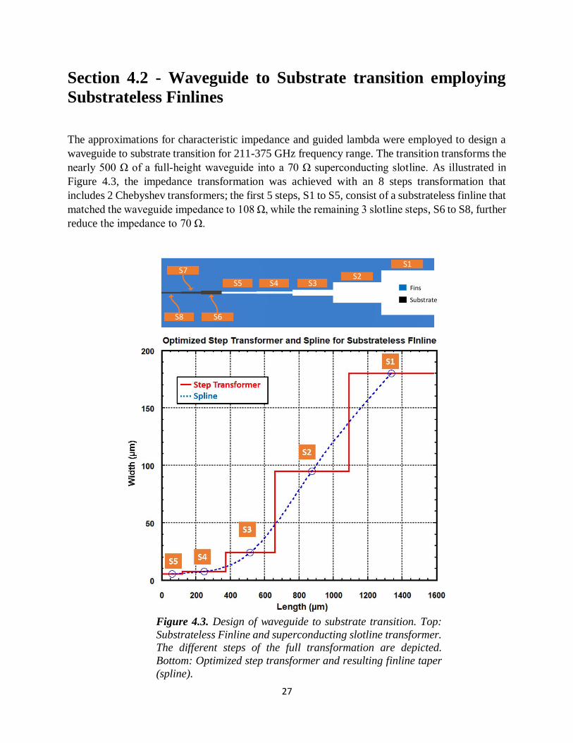
The approximations for characteristic impedance and guided lambda were employed to design a
waveguide to substrate transition for 211-375 GHz frequency range. The transition transforms the
nearly 500 Ω of a full-height waveguide into a 70 Ω superconducting slotline. As illustrated in
Figure 4.3, the impedance transformation was achieved with an 8 steps transformation that
includes 2 Chebyshev transformers; the first 5 steps, S1 to S5, consist of a substrateless finline that
matched the waveguide impedance to 108 Ω, while the remaining 3 slotline steps, S6 to S8, further
reduce the impedance to 70 Ω.
S1
S2S3S4S5
S6S8
S7
Fins
Substrate
Figure 4.3. Design of waveguide to substrate transition. Top:
Substrateless Finline and superconducting slotline transformer.
The different steps of the full transformation are depicted.
Bottom: Optimized step transformer and resulting finline taper
(spline).
28
The taper shown in Figure 4.3 was obtained after drawing a spline curve through the centre of each
step. The spline definition generates a smoother impedance transition since it reduces the effect of
step discontinuities in the response [66].
Employing the finline taper and the superconducting slotline transformer, the waveguide to
substrate transition illustrated in Figure 4.4a was designed. The transition incorporates
superconducting Nb fins deposited over 30 µm Si substrate. Moreover, the Nb fins are grounded
to the copper block through Au beamleads that extend 100 µm beyond the substrate. The Au
beamleads overlaps the superconducting fins and follow a similar spline, but they are offset from
the Nb edge to avoid losses in the Au. When the waveguide split block is closed, the beamleads
are clamped and pressed between the two halves, as shown in Figure 4.4a and c.
Consequently, the device is supported only by the beamleads and the substrate is suspended inside
the waveguide block. It is important to note that the waveguide width was increased from 400 µm
600µm 400µm
Niobium
Silicon
Gold
(a)
(d) (e)
40
0x4
20
µm
W
ave
gu
ide
80
0x4
20
µm
W
aveg
uid
e
200µm
290µm
(b)
Substrate
30µm Silicon
5µm Gold400nm Nb
200
µm
Copper Block
(c)
1940µm
10µm
Figure 4.4. Waveguide to substrate transition. (a) Transition mounted in the block. (b) Lateral view of
the structure mounted in the waveguide. (c) Transition viewed from slotline side. The different material
thicknesses are appreciated. For the sake of clarity, this image is shown not to scale. (d) Top view of
the transition. Au beamleads extend by 100 µm from each side of the silicon substrate. The dashed
lines illustrate the waveguide dimension. (e) The bottom view reveals the profile of the silicon substrate
and its overall length.
29
to 420 µm. This additional 20 µm facilitates the mounting of the device since a 10 µm gap is
created between the substrate and the waveguide wall.
As depicted in Figure 4.4b and c, the block height is reduced in 2 equal steps to obtain the
subcritical dimension 400x420 µm. This waveguide dimension prevents the propagation of
unwanted waveguide modes in the frequency of operation. The waveguide height variation is
introduced when the field has already concentrated between the fins, as shown in Figure 4.4b.
Thus, the change of waveguide height has almost no effect on the impedance of the transition. It is important to remark that a tolerance analysis was performed to investigate the sensitivity of
the different parameters of the device. It was concluded that the fabrication precision was required
to be ±1 μm for the step widths and ±5 μm for the step longitudes. A standard microfabrication
process can achieve this precision.
Back-to-Back Structure Superconducting Simulation
Since the S parameter characterization systems at the targeted frequency range 211-375 GHz make
use of waveguide extenders, it was developed a structure composed of two transitions in a back-
to-back arrangement for mounting in a split block waveguide. With a back-to-back structure, the
simulations and measurements can be easily compared. The back-to-back structure is shown in
Figure 4.5a. From the image, it can be seen that silicon tips have been added to the finline
structures. These silicon tips, which rest inside pockets in the block, facilitate handling and
alignment of the back-to-back finline sample.
The electromagnetic performance of the back-to-back structure at 4 K was simulated in Ansys
HFSS employing two different approaches. Firstly, the superconducting Nb layer was simulated
as a perfect conductor (PEC). Secondly, the complex surface impedance of the superconductor
was calculated following the BCS theory. Moreover, the surface impedance values were computed
for 450 nm of Nb in the frequency range 211-375 GHz. Afterwards, the complex impedance was
applied as an impedance boundary to the fins. This procedure was based on the superconductor
simulation detailed in [67] and the method proposed in [68] for the superconducting microstrips
simulation.
The PEC and superconducting simulations are compared in Figure 4.5b. It is seen that both
simulations predict an insertion loss of less than 0.6 dB, and a return loss better than 15 dB over
the whole band, i.e. 211-375 GHz. However, the superconducting approximation response seems
to be shifted to higher frequencies. This shift may be explained by the reactive component of the
surface impedance, which is not present in the PEC approximation. Nevertheless, the agreement
of the simulations indicates that the functions developed in [Paper B] give a reasonable
approximation for substrateless finline and superconducting slotline design. In the case of
superconducting finlines and slotlines, the magnetic field penetrates into the superconductor from
both faces of the superconducting thin film that forms the fins. Therefore, the PEC approximations
developed in [Paper B] will remain valid as far as the fins are much thicker than twice the London
penetration depth λL of the superconducting material, e.g. 180 nm for a thin-film Nb layer.

30
Top Part
Bottom Part
Silicon Tip
Steps
(a)
(b)
Figure 4.5. Back to Back transition. (a) Transition mounted in the block. The
upper and lower halves of the block are depicted separately. (b) S parameter
simulation of back-to-back structure employing PEC and Superconductor
approximations.
31
Section 4.3 - Bending of the fabricated Structure
The samples were fabricated following the process presented in [Paper B]. After the samples were
released, they were inspected under the microscope. From this analysis, it was appreciated that the
back-to-back structures were bent. The bending was further analyzed by employing an optical 3D
profilometer. The inspection results depicted in Figure 4.6 show that the structure symmetrically
bends along the X-axis. This deformation may be the result of the fabrication process. In particular,
the Nb layer is deposited with a compressive stress of about 200 to 300 MPa, which may cause the
bending of the finline structure. Stress-free Nb films are hard to accurately achieved, while tensile
stressed films have the substantial disadvantage of worse adhesion and porous structure, which
degrade their superconductive properties [69]. Therefore, compressively stressed Nb film is
A
B
Figure 4.6. Profile analysis of the fabricated back-to-back structure.
The 3D representation clearly show the structure is bending along the
X axis. The profile graph for the slice “A-B” shows that the structure
is bended 55 µm with respect to its center.
32
employed as it provides the highest superconducting properties, as well as having the least
developed surface topography for the film [69].
The deformation of the structure complicates the correct mounting of the samples in the block.
Nevertheless, the considerable flexibility of the thin silicon substrate allowed to reshape of the
back-to-back structure. With the help of a wire bonding machine, the beamleads were carefully
pressed against the block surface to flatten the structure. It is important to remark that the bonding
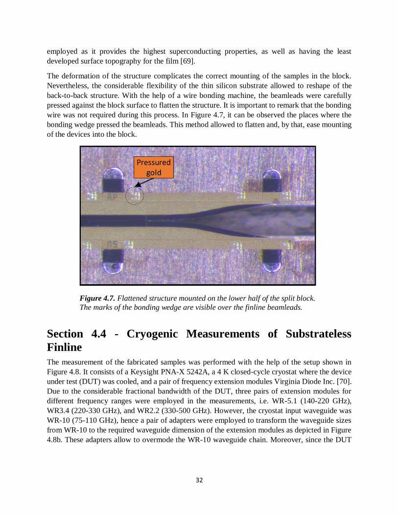
wire was not required during this process. In Figure 4.7, it can be observed the places where the
bonding wedge pressed the beamleads. This method allowed to flatten and, by that, ease mounting
of the devices into the block.
Section 4.4 - Cryogenic Measurements of Substrateless
Finline
The measurement of the fabricated samples was performed with the help of the setup shown in
Figure 4.8. It consists of a Keysight PNA-X 5242A, a 4 K closed-cycle cryostat where the device
under test (DUT) was cooled, and a pair of frequency extension modules Virginia Diode Inc. [70].
Due to the considerable fractional bandwidth of the DUT, three pairs of extension modules for
different frequency ranges were employed in the measurements, i.e. WR-5.1 (140-220 GHz),
WR3.4 (220-330 GHz), and WR2.2 (330-500 GHz). However, the cryostat input waveguide was
WR-10 (75-110 GHz), hence a pair of adapters were employed to transform the waveguide sizes
from WR-10 to the required waveguide dimension of the extension modules as depicted in Figure
4.8b. These adapters allow to overmode the WR-10 waveguide chain. Moreover, since the DUT
Pressured gold
Figure 4.7. Flattened structure mounted on the lower half of the split block.
The marks of the bonding wedge are visible over the finline beamleads.

33
waveguide size is 800x420 um, an additional pair of adapters were located at the 4K stage inside
the cryostat, as illustrated by Figure 4.8c.
The major challenge in measuring S parameters at cryogenic temperatures lies in the calibration
inside a cryostat, especially at high frequencies where waveguide systems are employed. The
reduction of the waveguide chain losses during cooling dramatically affects the reference planes
Frequency Extension Modules
VNA
4K PLATE
Calibration Planes
DUT
WR-10Adapters WR-10 to
800x400µm
DUT
4K
(c)
(a)
(b) Adapter WR-3.4 to WR-10
WR-10
Figure 4.8. Measurement setup. (a) WR-3.4 frequency extension
modules and VNA (b) The extension modules are connected to the WR-
10 waveguide chain using adapters. The calibration plane is located
outside the cryostat. (c) Waveguide chain inside the cryostat.
34
calibrated at warm inside the cryostat since the warm calibration overestimates the losses. The
shift of the calibration planes could be corrected by measuring a short circuit standard at 4K, as
described in [71]. This method for cryogenic measurements is frequently applied at lower
frequencies where coaxial cables are employed. Nonetheless, it is not practical at higher
frequencies due to the waveguide chain's thermal contraction. This shrinking is comparable to the
guided wavelength, thus, it is not possible to accurately correct the room temperature calibrations.
Therefore, an alternative measurement procedure using waveguide frequency extension modules
was developed to characterize the insertion loss of back-to-back substrateless finline structures. A
standard warm TRL calibration was applied to position the calibration planes at the input of the
cryostat, as depicted in Figure 4.8b. This calibration served to measure the DUT and a waveguide
thru at 4K and 10K. The waveguide chain was identical for both measurements, which allows the
comparison of the DUT insertion loss with the waveguide Thru. As a result, the relative insertion
loss of the DUT was obtained and compared with the simulation. The same procedure was repeated
for the three frequency bands.
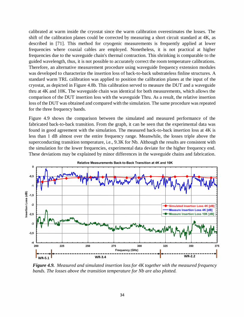
Figure 4.9 shows the comparison between the simulated and measured performance of the
fabricated back-to-back transition. From the graph, it can be seen that the experimental data was
found in good agreement with the simulation. The measured back-to-back insertion loss at 4K is
less than 1 dB almost over the entire frequency range. Meanwhile, the losses triple above the
superconducting transition temperature, i.e., 9.3K for Nb. Although the results are consistent with
the simulation for the lower frequencies, experimental data deviate for the higher frequency end.
These deviations may be explained by minor differences in the waveguide chains and fabrication.
Figure 4.9. Measured and simulated insertion loss for 4K together with the measured frequency
bands. The losses above the transition temperature for Nb are also plotted.
35
Section 4.5 - State of the Art Comparison
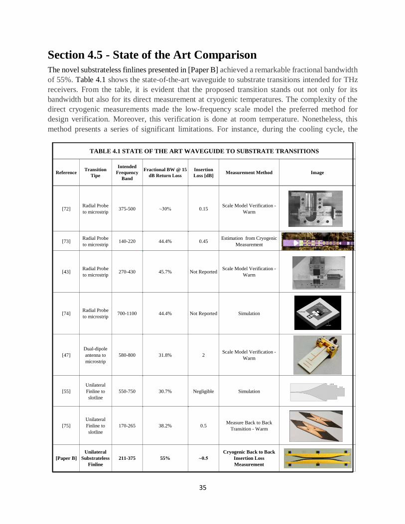
The novel substrateless finlines presented in [Paper B] achieved a remarkable fractional bandwidth
of 55%. Table 4.1 shows the state-of-the-art waveguide to substrate transitions intended for THz
receivers. From the table, it is evident that the proposed transition stands out not only for its
bandwidth but also for its direct measurement at cryogenic temperatures. The complexity of the
direct cryogenic measurements made the low-frequency scale model the preferred method for
design verification. Moreover, this verification is done at room temperature. Nonetheless, this
method presents a series of significant limitations. For instance, during the cooling cycle, the
ReferenceTransition
Tipe
Intended
Frequency
Band
Fractional BW @ 15
dB Return Loss
Insertion
Loss [dB]Measurement Method Image
[72]Radial Probe
to microstrip375-500 ⁓30% 0.15
Scale Model Verification -
Warm
[73]Radial Probe
to microstrip140-220 44.4% 0.45
Estimation from Cryogenic
Measurement
[43]Radial Probe
to microstrip270-430 45.7% Not Reported
Scale Model Verification -
Warm
[74]Radial Probe
to microstrip700-1100 44.4% Not Reported Simulation
[47]
Dual-dipole
antenna to
microstrip
580-800 31.8% 2Scale Model Verification -
Warm
[55]
Unilateral
Finline to
slotline
550-750 30.7% Negligible Simulation
[75]
Unilateral
Finline to
slotline
170-265 38.2% 0.5Measure Back to Back
Transition - Warm
[Paper B]
Unilateral
Substrateless
Finline
211-375 55% ⁓0.5
Cryogenic Back to Back
Insertion Loss
Measurement
TABLE 4.1 STATE OF THE ART WAVEGUIDE TO SUBSTRATE TRANSITIONS

36
thermal contraction of the various materials and the rise of stress can easily break ultrathin silicon
devices. The survival of the device to a cooling cycle cannot be assessed adequately with warm
measurements. Furthermore, the impact of the fabrication and mounting tolerances cannot be
evaluated with low-frequency scale models. To the best knowledge of the authors, the insertion
loss measurement presented in [Paper B] constituted the first verification of a back-to-back
structure at cryogenic temperatures.
This ultrawide bandwidth of substrateless finline transitions opens new possibilities for the design
of receivers in radio astronomy applications. In particular, the presented substrateless finline
allows covering ALMA band 6 (211-275 GHz) and ALMA band 7 (275-375GHz) simultaneously
[16]. Nevertheless, the applicability of this new type of finline is not limited to radio astronomy
applications, but it can be employed in a wide range of mm and sub-mm applications. For instance,
it may be applied in the THz communication systems that have increasingly drawn attention in
recent years [5]. Moreover, the design procedure detailed in [Paper B] might be employed for
different frequency ranges, making substrateless finlines an attractive solution for a great variety
of wideband applications.
37
Chapter 5 - Ongoing Research: Ultrawideband Slotline
to Microstrip Transition for 211-375 GHz based on
Marchand Balun
The transition based on Substrateless finlines detailed in Chapter 4 transforms a waveguide
impedance into a slotline. Since fabricating slotlines with small characteristic impedances below
10 Ohm is not practical at mm-wave and THz frequencies, most modern SIS mixers rely on other
types of transmission line, e.g. thin-film microstrip lines [45]. Therefore, the need for an additional
transition step from slotline into microstrip becomes clear. To address this need, the ongoing
research is focused on the design, fabrication and cryogenic measurement of a slotline to microstrip
transition covering the frequency range 210-375 GHz.
The literature review on existing microstrip to slotline transitions presented in Section 2.4 shows
the Marchand baluns as a promising solution due to their compactness and straightforward design.
However, to the author's best knowledge, these baluns have not been previously investigated for
sub-mm applications. In this chapter, the design and fabrication of a superconducting Marchand
balun for future wideband mixer chip design.
Section 5.1 - Transition design
The proposed transition depicted in Figure 5.1 is based on a third-order Chebyshev Marchand
balun [56]. The balun consists of a microstrip and a slotline that lie perpendicular to each other.
The structure is patterned on top of a 30 µm Si substrate compatible with the finline structure
presented in [Paper B]. The slotline and the microstrip are defined by 450 nm of superconducting
Nb, and they separated by a layer of 1.3 µm SiO2. This particular dielectric thickness was chosen
to achieve the required impedance while keeping the microstrip width at the level of a few µm, i.e.
compatible with the available microfabrication process.
Figure 5.2 outlines the different impedances employed in the transition as an equivalent circuit
diagram. The transition transforms a 60 Ohms slotline, referred to as ZoS, into a 45 Ohms
microstrip, denominated as ZoM. The transformation is accomplished with two stubs: an open
circuit microstrip stub and a short circuit slotline stub, with Z1 and Z2 characteristic impedances,
respectively. Besides, Z3 is realized as a λ/4 slotline section that matches the intersection
impedance to ZoS. The procedure to calculate the impedances Z1, Z2 and Z3 are detailed in
Appendix I.

38
Z1
Z2
ZoM
Z3ZoS
Microstrip
Slotline
Nb Microstrip
Nb Ground
Silicon
SiO2
450 nm Nb Microstrip
450 nm Nb Ground
1.3 µm SiO2
30 µm Si
(a)
(b)
Figure. 5.1. Proposed slotline to microstrip Marchand
Balun transition. (a) Top view of the transition. (b) Lateral
view of the structure where the different layers and
thicknesses are detailed.
Z2
Z1
ZoM ZoSZ3
Figure 5.2. Equivalent circuit diagram of the proposed third
order Chebyshev Marchand Balun transition. The microstrip
impedance ZoM is 45 Ohm while the slotline impedance ZoS
is 60 Ohm. The impedances Z1 and Z3 are realized with
slotlines. Meanwhile, the short circuit stub with a
characteristic impedance Z2 is realized as a microstrip.

39
Section 5.2 – Back-to-Back Electromagnetic Simulation
After the dimensions of the transmission lines were defined, the complete Marchand Balun was
simulated and optimized for minimizing the insertion loss in the full-wave 3-D simulator Ansys
HFSS [64]. Figure 5.3a shows that the optimization was performed with a back-to-back layout,
where both input and output are microstrips. This layout responds to the particular characteristics
of the simulator, where microstrips are simpler to excite than slotlines. Moreover, the
45 Ohm Lumped Ports
(a)
(b)
Figure 5.3. Electromagnetic Simulation (a) Simulated back-to-back
structure. The microstrip ports were excited with 45 Lumped Ports. (b)
Simulated S parameters Marchand Balun Transition in a back-to-back
arrangement.

40
superconducting Nb was simulated as a perfect conductor. This approximation was appropriate
since the dielectric thickness is several times the thickness of Nb, i.e. 1.3 µm and 0.45 µm,
respectively. Under this condition, the superconducting microstrip impedance resembles a
microstrip with perfect conductor electrodes [67, 68].
The simulation results for the back-to-back balun are presented in Figure 5.3b, where the calculated
and optimized transition can be compared. The graph shows that the simulated return loss for the
optimized back-to-back Marchand Balun is better than 25 dB in the whole band. Furthermore, the
insertion loss is above -0.1 dB in the entire frequency range.
Section 5.3 - Test Chip Design
To fabricate and assess the performance of the back-to-back Marchand Balun, the structure must
be integrated with a waveguide to microstrip transition. Thus, the back-to-back transition was
integrated with E-probes. However, a single probe cannot cover the entire frequency band
adequately. Therefore, two versions of the test chip for the frequency range 211-295GHz and 295-
375 GHz were designed. A separate probe was designed and optimized for each frequency range.
Both test chips included a straight section of microstrip that connects the probe with a 90°
microstrip bend terminated in 45 Ohm, i.e. ZoM. The microstrip bend was introduced to
accommodate the Marchand Balun transition in a back-to-back layout. The chip is grounded
through a 5 µm thick Au beamleads that extend 80 µm beyond the silicon substrate. The beamleads
provide an electrical connection between the niobium ground layer and the waveguide block since
the gold is clamped and pressed between the two waveguide halves. The waveguide size of the
blocks is 800x400 µm to cover the entire frequency range 211-295GHz. The samples were
fabricated in house following the procedure detailed in Appendix II.
Section 5.4 - Ongoing Work
The characterization of the test chips at cryogenic temperatures is ongoing. Figure 5.4 illustrates
the fabricated chip and the measurement setup. The setup includes waveguide bends with
integrated waveguide size adapters from 2540x1270 µm (WR-10) to 800x400 µm. These adapters
are employed to connect the waveguide blocks, where the fabricated chips are mounted, to the
existing WR-10 waveguide chain of the cryostat. The chips are measured employing the technique
described in [Paper B], i.e. the insertion loss is compared with a waveguide thru at 4 K. This
approach allows for a straightforward comparison between measurements and simulation.
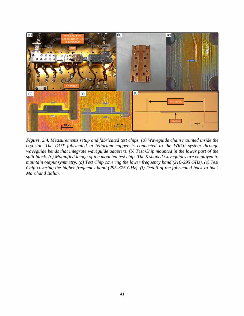
41
(a)
DUT
4K Plate
Waveguide Bend and adapter WR-10
to 800x400µm
(b) (c)
(d) (e) (f)
Microstrips
Slotline
500 µm 500 µm 100 µm
Figure. 5.4. Measurements setup and fabricated test chips. (a) Waveguide chain mounted inside the
cryostat. The DUT fabricated in tellurium copper is connected to the WR10 system through
waveguide bends that integrate waveguide adapters. (b) Test Chip mounted in the lower part of the
split block. (c) Magnified image of the mounted test chip. The S shaped waveguides are employed to
maintain output symmetry. (d) Test Chip covering the lower frequency band (210-295 GHz). (e) Test
Chip covering the higher frequency band (295-375 GHz). (f) Detail of the fabricated back-to-back
Marchand Balun.
42
Chapter 6 - Conclusion and Future Outlook
The next generation of radio astronomy receivers demands a considerable improvement in the RF
bandwidths of passive devices. To address this need, a series of ultra-wideband passive devices
have been presented in this thesis.
Firstly, a 90° step twist for the frequency range 140-220 GHz was presented. In contrast to existing
designs, the twist presented in this work avoids sharp corners, which greatly enhances
manufacturability through direct milling without compromising its performance or compactness.
Secondly, a new type of finline was developed, i.e. the substrateless finlines. This novel approach
improves the matching with waveguides and reduces the overall losses in the substrate.
Consequently, substrateless finlines are an attractive solution for the design of ultra-wideband
waveguide to substrate transitions. In this thesis, a waveguide to substrate transition with 55%
fractional bandwidth (211-375 GHz) was designed, simulated and measured at cryogenic
temperatures. To the authors' best knowledge, the insertion loss measurement presented in this
work constituted the first verification of a back-to-back structure at cryogenic temperatures.
The need for further transition from slotline to microstrip motivates the ongoing research on
Marchand Baluns. In this work, a slotline to microstrip transition was designed and simulated for
the frequency range 211-375 GHz. The simulations showed promising results, and characterization
at 4 K is ongoing.
Figure 6.1a shows a conceptual integration of the Marchand Balun with substrateless finline to
design a waveguide to microstrip transition. This transition could be employed for the future
design of broadband SIS mixers receivers. In Figure 6.1b, a conceptual block diagram for a
sideband separating receiver is depicted. In the block diagram, the RF and LO signals are
transferred to the substrate with the waveguide to microstrip transition shown in Figure 6.1a.
Moreover, the RF 90° hybrid and power divider could be integrated on the same chip.
Even though the devices presented in this work were meant for radio astronomy receivers, other
applications at THz frequencies could possibly benefit from this development. Furthermore, the
presented designs can be easily scaled down to lower frequencies, extending their applicability to
a large number of broadband systems.
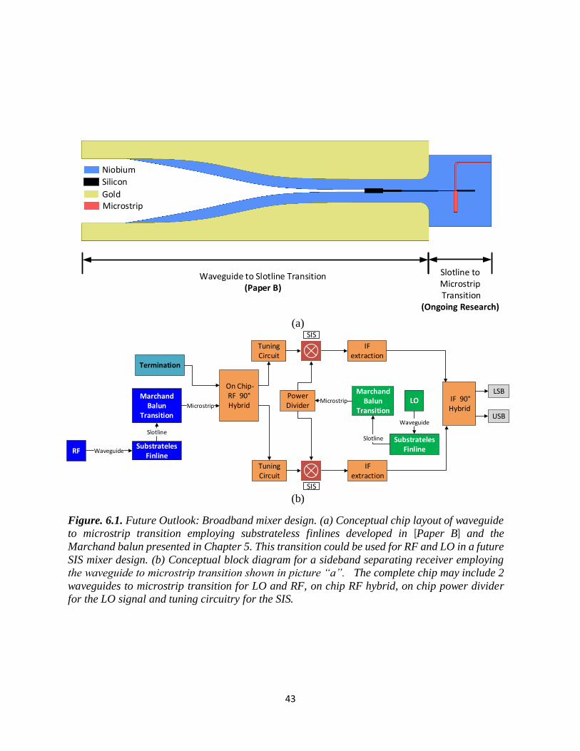
43
Niobium
Silicon
GoldMicrostrip
Waveguide to Slotline Transition (Paper B)
Slotline to Microstrip Transition
(Ongoing Research)
(a)
On Chip- RF 90° Hybrid
Substrateles Finline
Marchand Balun
Transition
Termination
Microstrip
Slotline
RF Waveguide
Substrateles Finline
Marchand Balun
Transition
Microstrip
Slotline
LO
Waveguide
Tuning Circuit
IF extraction
Power Divider
Tuning Circuit
IF extraction
IF 90° Hybrid
USB
LSB
SIS
SIS
(b)
Figure. 6.1. Future Outlook: Broadband mixer design. (a) Conceptual chip layout of waveguide
to microstrip transition employing substrateless finlines developed in [Paper B] and the
Marchand balun presented in Chapter 5. This transition could be used for RF and LO in a future
SIS mixer design. (b) Conceptual block diagram for a sideband separating receiver employing
the waveguide to microstrip transition shown in picture “a”. The complete chip may include 2
waveguides to microstrip transition for LO and RF, on chip RF hybrid, on chip power divider
for the LO signal and tuning circuitry for the SIS.

44
(I.1)
(I.2)
(I.3)
(I.4)
(I.5)
Appendix I - Simplified equations for third-order
Chebyshev Marchand balun calculation.
The following equations can be used for calculating a third-order Marchand Balun [56] and serve
as a starting point for optimization:
𝑧3 = √𝑧𝑜𝑠
𝑧2 = −√𝑧𝑜𝑠 + (𝑧𝑜𝑠 +𝛼2 + 𝛽2
(𝛼 − 1) tan2 𝜃)
12
𝑧1 =𝛼2 + 𝛽(𝛽 + 𝑧2 tan 𝜃)
𝛼2 + (𝛽 + 𝑧2 tan 𝜃)2𝑧2 𝑡𝑎𝑛2 𝜃
𝛼 = 𝑧𝑜𝑠(1 + tan2 𝜃
1 + 𝑧𝑜𝑠 𝑡𝑎𝑛2𝜃)
𝛽 = √𝑧𝑜𝑠 (1 − 𝑧𝑜𝑠)tan 𝜃
1 + 𝑧𝑜𝑠 tan2 𝜃
The terms 𝛼 and 𝛽 are used solely to simplify the presentation of the equations. Meanwhile, the
variable 𝜃 , express in degrees, defines the theoretical bandwidth of the Chebyshev response. The
relation between 𝜃 and the overall bandwidth of the transformer was numerically calculated in
[56], showing an inverse nonlinear relation between these 2 variables. It is important to note that
all the impedances have been normalized by ZoM in the equations.
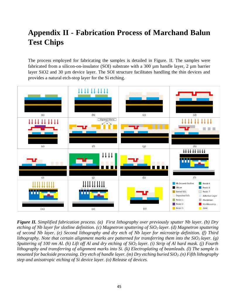
45
Appendix II - Fabrication Process of Marchand Balun
Test Chips
The process employed for fabricating the samples is detailed in Figure. II. The samples were
fabricated from a silicon-on-insulator (SOI) substrate with a 300 µm handle layer, 2 µm barrier
layer SiO2 and 30 µm device layer. The SOI structure facilitates handling the thin devices and
provides a natural etch-stop layer for the Si etching.
Figure II. Simplified fabrication process. (a) First lithography over previously sputter Nb layer. (b) Dry
etching of Nb layer for slotline definition. (c) Magnetron sputtering of SiO2 layer. (d) Magnetron sputtering
of second Nb layer. (e) Second lithography and dry etch of Nb layer for microstrip definition. (f) Third
lithography. Note that certain alignment marks are patterned for transferring them into the SiO2 layer. (g)
Sputtering of 100 nm Al. (h) Lift off Al and dry etching of SiO2 layer. (i) Strip of Al hard mask. (j) Fourth
lithography and transferring of alignment marks into Si. (k) Electroplating of beamleads. (l) The sample is
mounted for backside processing. Dry etch of handle layer. (m) Dry etching buried SiO2. (n) Fifth lithography
step and anisotropic etching of Si device layer. (o) Release of devices.

46
After carefully cleaning the handle layer surface, a film of 450nm Nb layer is deposited by dc
magnetron. Afterwards, the first lithography shown in Figure II.a creates a photoresist soft-mask
over the Nb layer. This mask is later employed to define the slotline by dry etching the Nb layer
in a reactive ion etching (RIE) process. Then, the 1.3 µm SiO2 layer is deposit by a reactive RF
magnetron sputtering. Furthermore, a second 450 nm Nb layer is deposited over the SiO2 in the
same vacuum run. The microstrip lines are created over this last Nb layer with a second lithography
and dry-etching, as depicted in Figure II.e. This is followed by the third lithography shown in
Figure II.f and the sputtering of a 100 nm Al layer, as illustrated by Figure II.g. The lift-off in
acetone of the Al layer defines a hard mask for the SiO2 dry-etching process shown in Figure II.h.
In addition, in this process stage, specially designed alignment marks are patterned in the SiO2.
This oxide layer will act as a hard mask for further transferring these alignment marks into the
backside of the Si device layer with the help of a Bosh process. The deep Si etching by the Bosch
process is depicted in Figure II.j. The Figure demonstrates how a thick photoresist allows the deep
etching of the alignment marks but protects the rest of the sample. The alignment marks transfer
will prove to be helpful in the last steps of the process since they will transform backside
lithography into frontside lithography. This is advantageous since a better alignment could be
easily obtained in frontside lithography.
After removing the thick photoresist, the beamleads are created through electroplating process, as
depicted in Figure II.k. Afterwards, the chip is mounted upside down on a 4-inch Si carrier wafer
for backside processing. The mounting process involves a release layer and an adhesive layer. The
subsequent dry etch illustrated in Figure II.l and Figure II.m are employed to remove the handle
layer and the buried oxide layer, respectively. The final lithography defines the chip shapes and
uses the alignment marks patterned in the backside of the device layer. Therefore, a thick
photoresist etch mask could be created on the backside. This soft-mask is used for the final
anisotropic etching that complete the device definition. Finally, the devices are released when the
adhesive and release layer are dissolved in a solvent.
47
Bibliography
[1] ROGALSKI, A.; SIZOV, F. Terahertz detectors and focal plane arrays. Opto-electronics Review, 2011, vol.
19, no 3, p. 346-404.
[2] PICKWELL, E.; WALLACE, V. P. Biomedical applications of terahertz technology. Journal of Physics D:
Applied Physics, 2006, vol. 39, no 17, p. R301.
[3] FERGUSON, Bradley; ZHANG, Xi-Cheng. Materials for terahertz science and technology. Nature
materials, 2002, vol. 1, no 1, p. 26-33.
[4] FARRAH, Duncan, et al. far-infrared instrumentation and technological development for the next
decade. Journal of Astronomical Telescopes, Instruments, and Systems, 2019, vol. 5, no 2, p. 020901.
[5] SONG, Ho-Jin; NAGATSUMA, Tadao. Present and future of terahertz communications. IEEE transactions
on terahertz science and technology, 2011, vol. 1, no 1, p. 256-263.
[6] BILLADE, Bhushan, et al. Performance of the first ALMA band 5 production cartridge. IEEE Transactions
on Terahertz Science and Technology, 2012, vol. 2, no 2, p. 208-214.
[7] RASHID, Hawal, et al. Frequency multiplier based on distributed superconducting tunnel junctions: Theory,
design, and characterization. IEEE Transactions on Terahertz Science and Technology, 2016, vol. 6, no 5, p.
724-736.
[8] KRAUSE, Sascha, et al. Noise and IF gain bandwidth of a balanced waveguide NbN/GaN hot electron
bolometer mixer operating at 1.3 THz. IEEE Transactions on Terahertz Science and Technology, 2018, vol.
8, no 3, p. 365-371.
[9] ARMSTRONG, Carter M. The truth about terahertz. IEEE Spectrum, 2012, vol. 49, no 9, p. 36-41.
[10] COLLABORATION, Event Horizon Telescope, et al. First M87 event horizon telescope results. The shadow
of the supermassive black hole. Astrophys. J. Lett, 2019, vol. 875, no 1, p. L1.
[11] “NOrthern Extended Millimeter Array NOEMA”, IRAM Institut de Radioastronomie Millimétrique.
[Online]. Available: https://www.iram-institute.org/EN/noema-project.php
[12] "Atacama Pathfinder Experiment APEX" [Online]. ESO, Max-Planck-Institut für Radiastonomie, Onsala
Rymdobservatorium, Available: http://www.apex-telescope.org/ns/
[13] "Atacama Large Millimiter/submillimiter Array ALMA", ESO. [Online]. Available:
https://www.almaobservatory.org/en/home/
[14] GREAVES, Jane S., et al. Phosphine gas in the cloud decks of Venus. Nature Astronomy, 2020, p. 1-10.
[15] MATSUSHITA, Yuko, et al. A very compact extremely high velocity flow toward MMS 5/OMC-3 revealed
with ALMA. The Astrophysical Journal, 2019, vol. 871, no 2, p. 221.
[16] CARPENTER, John, et al. The ALMA Development Program: Roadmap to 2030. arXiv preprint
arXiv:2001.11076, 2020.
[17] KRAUS, John D., et al. Radio astronomy. Powell, Ohio: Cygnus-Quasar Books, 1986.
[18] P.Y. Aghdam, "Characterization of the Specific Capacitance of Superconducting Tunnel Junctions",
Chalmers University of Technology, Gothenburg, 2015.
[19] MORGAN, Matthew; WEINREB, Sander. A monolithic HEMT diode balanced mixer for 100-140 GHz.
IEEE, 2001.
[20] KOOI, Jacob W., et al. Quantum Limited SIS Receiver Technology for the Detection of Water Isotopologue
Emission from Comets. IEEE Transactions on Terahertz Science and Technology, 2020, vol. 10, no 6, p.
569-582.
[21] WILSON, Thomas L.; ROHLFS, Kristen; HÜTTEMEISTER, Susanne. Tools of radio astronomy. Berlin:
Springer, 2009.
[22] BARYSHEV, A. M., et al. The ALMA Band 9 receiver - Design, construction, characterization, and first
light. Astronomy & Astrophysics, 2015, vol. 577, p. A129.
[23] KERR, Anthony R., et al. Development of the ALMA band-3 and band-6 sideband-separating SIS
mixers. IEEE Transactions on Terahertz Science and Technology, 2014, vol. 4, no 2, p. 201-212.
[24] YAGOUBOV, Pavel, et al. Wideband 67− 116 GHz receiver development for ALMA Band 2. Astronomy &
Astrophysics, 2020, vol. 634, p. A46.

48
[25] DEAL, W. R., et al. InP HEMT integrated circuits operating above 1,000 GHz. 2016 IEEE International
Electron Devices Meeting (IEDM). IEEE, 2016. p. 29.1. 1-29.1. 4.
[26] MOSCHETTI, Giuseppe, et al. A 183 GHz metamorphic HEMT low-noise amplifier with 3.5 dB noise
figure. IEEE Microwave and Wireless Components Letters, 2015, vol. 25, no 9, p. 618-620.
[27] POZAR, David M. Microwave engineering. John Wiley & sons, 2011.
[28] HENKE, Doug; CLAUDE, Stéphane. Design of a 70–116 GHz W-band turnstile OMT. 2014 44th European
Microwave Conference. IEEE, 2014. p. 456-459.
[29] Belitsky, V., Lapkin, I., Fredrixon, M., Meledin, D., Sundin, E., Billade, B., ... & Koops, A. (2018). SEPIA–
a new single pixel receiver at the APEX telescope. Astronomy & Astrophysics, 612, A23.
[30] MARAL, Gerard; BOUSQUET, Michel; SUN, Zhili. Satellite communications systems: systems, techniques
and technology. John Wiley & Sons, 2020.
[31] ZENG, Lingzhen, et al. A Compact Machinable 90° Waveguide Twist for Broadband Applications. IEEE
Transactions on Microwave Theory and Techniques, 2020, vol. 68, no 7, p. 2515-2520.
[32] BARALIS, Massimo, et al. Full-wave design of broad-band compact waveguide step-twists. IEEE
microwave and wireless components letters, 2005, vol. 15, no 2, p. 134-136.
[33] AL-TARIFI, Muhannad A.; FILIPOVIC, Dejan S. Design and fabrication of a full W-band multi-step
waveguide 90° twist. IEEE Microwave and Wireless Components Letters, 2016, vol. 26, no 11, p. 903-905.
[34] RUIZ-CRUZ, Jorge A.; MONTEJO-GARAI, José R.; REBOLLAR, Jesús M. Multi-section bow-tie steps
for full-band waveguide polarization rotation. IEEE Microwave and Wireless components letters, 2010, vol.
20, no 7, p. 375-377.
[35] KIRILENKO, Anatoliy A.; KULIK, Dmitriy Y.; RUD, Leonid A. Compact 90° Twist Formed by a Double-
Corner-Cut Square Waveguide Section. IEEE transactions on microwave theory and techniques, 2008, vol.
56, no 7, p. 1633-1637.
[36] LENZING, H. F.; GANS, M. J. Machined waveguide twist. IEEE transactions on microwave theory and
techniques, 1990, vol. 38, no 7, p. 942-944.
[37] ROSENBERG, Uwe; BORNEMANN, Jens; AMARI, Smain. A compact and broadband 90-degree
waveguide twist transformer for integrated waveguide subsystems. 2001.
[38] ASAO, Hideki; HIRAIWA, Go; KATAYAMA, Akiko. A compact 90-degree twist using novel ridged
waveguide for integrated waveguide subsystems. 2006 European Microwave Conference. IEEE, 2006. p.
1185-1188.
[39] KIRILENKO, Anatoliy A., et al. Comparative analysis of novel compact and usual smooth 90-degree twists.
Proceedings of International Conference on Antenna Theory and Techniques. 2009. p. 328-330.
[40] CHEN, Lihan, et al. A Micromachined Terahertz Waveguide 90° Twist. IEEE microwave and wireless
components letters, 2011, vol. 21, no 5, p. 234-236.
[41] CHATTOPADHYAY, Goutam, et al. Submillimeter-Wave 90° Polarization Twists for Integrated
Waveguide Circuits. IEEE microwave and wireless components letters, 2010, vol. 20, no 11, p. 592-594.
[42] WITHINGTON, S.; YASSIN, G. An investigation of the input impedance of a microstrip probe in
waveguide. Proc. of the 8th Int. Symp. on Space Terahertz Technology. 1997.
[43] KOOI, J. W., et al. A full-height waveguide to thinfilm microstrip transition. Ninth International Conference
on Therahertz Electronics. 2001. p. 15-16.
[44] RISACHER, Christophe, et al. A 275–370 GHz Receiver Employing Novel Probe Structure. International
journal of infrared and millimeter waves, 2005, vol. 26, no 6, p. 867-879.
[45] BILLADE, Bhushan; PAVOLOTSKY, Alexey; BELITSKY, Victor. An SIS Mixer with 2hf/k DSB Noise
Temperature at 163-211 GHz Band. IEEE Transactions on Terahertz Science and Technology, 2013, vol. 3,
no 4, p. 416-421.
[46] LEONG, Kevin MKH, et al. A 340–380 GHz integrated CB-CPW-to-waveguide transition for sub-
millimeter-wave MMIC packaging. IEEE microwave and wireless components letters, 2009, vol. 19, no 6,
p. 413-415.
[47] TAN, Boon-Kok; WITHINGTON, Stafford; YASSIN, Ghassan. A compact microstrip-fed planar dual-
dipole antenna for broadband applications. IEEE Antennas and Wireless Propagation Letters, 2015, vol. 15,
p. 593-596.

49
[48] VASSILEV, V.; BELITSKY, Victor. Design of sideband separation SIS mixer for 3 mm band. Proceedings
of the Thirteenth International Symposium on Space Terahertz Technology. 2001. p. 373-382.
[49] MEIER, Paul J. Two new integrated-circuit media with special advantages at millimeter wavelengths. 1972
IEEE GMTT International Microwave Symposium. IEEE, 1972. p. 221-223.
[50] TAN, B.; YASSIN, Ghassan. Unilateral finline transition at THz frequencies. Proceedings of the Twentieth
International Symposium on Space Terahertz Technology. 2009. p. 263-266.
[51] TAN, Boon-Kok, et al. A 650 GHz unilateral finline SIS mixer fed by a multiple flare-angle smooth-walled
horn. IEEE Transactions on Terahertz Science and Technology, 2011, vol. 2, no 1, p. 40-49.
[52] CHANGFEI, Yao; JINPING, Xu; MO, Chen. Design of Ka-band antipodal finline mixer and
detector. Journal of Semiconductors, 2009, vol. 30, no 5, p. 055009.
[53] CHATTOPADHYAY, Goutam; CARLSTROM, John E. Finline ortho-mode transducer for millimeter
waves. IEEE microwave and guided wave letters, 1999, vol. 9, no 9, p. 339-341.
[54] YASSIN, Ghassan, et al. A 350-GHz SIS antipodal finline mixer. IEEE Transactions on microwave theory
and techniques, 2000, vol. 48, no 4, p. 662-669.
[55] TAN, Boon Kok. Development of coherent detector technologies for sub-millimetre wave astronomy
observations. Springer, 2015.
[56] TRIFUNOVIC, Velimir; JOKANOVIC, Branka. Review of printed Marchand and double Y baluns:
Characteristics and application. IEEE Transactions on Microwave Theory and Techniques, 1994, vol. 42, no
8, p. 1454-1462.
[57] KONGPOP, U., et al. Slotline stepped circular rings for low-loss microstrip-to-slotline transitions. IEEE
microwave and wireless components letters, 2007, vol. 17, no 2, p. 100-102.
[58] ZINIERIS, M. M.; SLOAN, R.; DAVIS, L. E. A broadband microstrip‐to‐slot‐line transition. Microwave
and optical technology letters, 1998, vol. 18, no 5, p. 339-342.
[59] SCHIEK, B.; KOHLER, J. An improved microstrip-to-microslot transition. IEEE Transactions on
Microwave Theory and Techniques, 1976, vol. 24, no 4, p. 231-233.
[60] DING, Jiang-Qiao; ZHAO, Yun; SHI, Sheng-Cai. A full WR-3 band and low-loss 90° waveguide twist based
on CNC. IEEE Transactions on Terahertz Science and Technology, 2019, vol. 10, no 1, p. 93-96.
[61] SCHIEBLICH, CHRISTIAN; PIOTROWSKI, J. K.; HINKEN, J. H. Synthesis of optimum finline tapers
using dispersion formulas for arbitrary slot widths and locations. IEEE transactions on microwave theory
and techniques, 1984, vol. 32, no 12, p. 1638-1645.
[62] NORTH, Chris; YASSIN, Ghassan; GRIMES, Paul. Rigorous analysis and design of finline tapers for high
performance millimetre and submillimetre detectors. Seventeenth International Symposium on Space
Terahertz Technology, 2006. p. 284-287.
[63] VALE, Christopher AW; MEYER, Petrie. Designing high-performance finline tapers with vector-based
optimization. IEEE Transactions on Microwave Theory and Techniques, 1999, vol. 47, no 12, p. 2467-2472.
[64] "High Frequency Electromagnetic Simulation Software HFSS", Ansys. [Online]. Available:
https://www.ansys.com/products/electronics/ansys-hfss
[65] ROZZI, Tullio, et al. Hybrid modes, substrate leakage, and losses of slotline at millimeter-wave
frequencies. IEEE transactions on microwave theory and techniques, 1990, vol. 38, no 8, p. 1069-1078.
[66] EBNABBASI, Khabat, et al. Taper design of Vivaldi and coplanar tapered slot antenna (TSA) by Chebyshev
transformer. IEEE transactions on antennas and propagation, 2012, vol. 60, no 5, p. 2252-2259.
[67] Kerr, A. R. Surface impedance of superconductors and normal conductors in EM simulators. MMA
Memo 245, 1999, p. 1-17.
[68] BELITSKY, Victor, et al. Superconducting microstrip line models at millimeter and sub-millimeter waves
and their comparison. 14th Space Terahertz Symposium, 2003, p. 456-465.
[69] IMAMURA, Takeshi; SHIOTA, Tetsuyoshi; HASUO, Shinya. Fabrication of high quality Nb/AlO/sub x/-
Al/Nb Josephson junctions. I. Sputtered Nb films for junction electrodes. IEEE Transactions on applied
superconductivity, 1992, vol. 2, no 1, p. 1-14.
[70] "Virginia Diodes Incorporated VDI" [Online]. Available: https://www.vadiodes.com/en/
[71] RASHID, Hawal, et al. Superconducting 4–8-GHz hybrid assembly for 2SB cryogenic THz receivers. IEEE
Transactions on Terahertz Science and Technology, 2014, vol. 4, no 2, p. 193-200.

50
[72] RISACHER, Christophe, et al. Waveguide-to-microstrip transition with integrated bias-T. IEEE Microwave
and Wireless Components Letters, 2003, vol. 13, no 7, p. 262-264.
[73] RASHID, Hawal, et al. Frequency multiplier based on distributed superconducting tunnel junctions: Theory,
design, and characterization. IEEE Transactions on Terahertz Science and Technology, 2016, vol. 6, no 5, p.
724-736.
[74] KOOI, J. W.; WALKER, C. K.; HESLER, J. A broad bandwidth suspended membrane waveguide to thin
film microstrip transition. 9th Int. Conference on Teraherz Electronics, 15th-16th October. 2001.
[75] TAN, Boon-Kok; YASSIN, Ghassan. A Slotline DC Block for Microwave, Millimeter, and Submillimeter
Circuits. IEEE Microwave and Wireless Components Letters, 2019, vol. 29, no 9, p. 583-585.
[76] TUCKER, John R.; FELDMAN, Marc J. Quantum detection at millimeter wavelengths. Reviews of Modern
Physics, 1985, vol. 57, no 4, p. 1055.
[77] NOVOSELOV, Evgenii; CHEREDNICHENKO, Sergey. Low noise terahertz MgB2 hot-electron bolometer
mixers with an 11 GHz bandwidth. Applied Physics Letters, 2017, vol. 110, no 3, p. 032601.
[78] ASAYAMA, Shin'ichiro, et al. Development of ALMA Band 4 (125–163 GHz) receiver. Publications of the
Astronomical Society of Japan, 2014, vol. 66, no 3.
[79] KOJIMA, Takafumi, et al. 275–500-GHz wideband waveguide SIS mixers. IEEE Transactions on Terahertz
Science and Technology, 2018, vol. 8, no 6, p. 638-646.
[80] DURAN, Carlos, et al. 4GREAT-a four-color receiver for high-resolution airborne terahertz
spectroscopy. IEEE Transactions on Terahertz Science and Technology, 2021, vol. 11, no. 2, pp. 194-204.
[81] VENTURI, Tiziana, et al. VLBI20-30: a scientific roadmap for the next decade. The future of the European
VLBI Network. preprint arXiv:2007.02347, 2020.
Paper A
López, C., Desmaris, V., Meledin, D., Pavolotsky, A., & Belitsky, V. (2020).
Design and Implementation of a Compact 90° Waveguide Twist with Machining
Tolerant Layout.
IEEE Microwave and Wireless Components Letters, 30(8), 741-744.

Paper B
López, C., Desmaris, V., Meledin, D., Pavolotsky, A., & Belitsky, V. (2020).
Waveguide-to-Substrate Transition Based on Unilateral Substrateless Finline
Structure: Design, Fabrication, and Characterization.
IEEE Transactions on Terahertz Science and Technology, 10(6), 668-676.


![Phase-matched scalable THz generation in two-color ... THz 10 THz 100 THz 1 PHz 10 PHz 300 m 30 m ... Kim presentation at Argonne 2012_no backup.ppt [Compatibility Mode] Author:](https://img.pdfslide.us/doc/110x75/5ac2b9eb7f8b9aca388e95a7/phase-matched-scalable-thz-generation-in-two-color-thz-10-thz-100-thz-1-phz.jpg)