Embed Size (px)
Citation preview
(Invited)
THz Local Oscillator Sources: Performance and Capabilities
Imran Mehdi*, E. Schlecht, G. Chattopadhyay, P. H. Siegel
California Institute of Technology, Jet Propulsion Laboratory
ABSTRACT Frequency multiplier circuits based on planar GaAs Schottky diodes have advanced significantly in the last decade. Useful power in the >1 THz range has now been demonstrated from a complete solid-state chain. This paper will review some of the technologies that have led to this achievement along with a brief look at future challenges. Keywords: Schottky diode multipliers, varactors, LO sources, THz technology
1. INTRODUCTION The current importance of astrophysics related, high-resolution spectroscopy, in the THz range is highlighted by the current build up of the Heterodyne Instrument for the Far Infrared (HIFI) on the European Space Agency’s Herschel Space Observatory [1,2,3]. HIFI will employ the highest frequency, highest sensitivity heterodyne receivers ever flown in space to discover, measure and map atomic and molecular gases in and around stars, nebulae and galaxies. A critical component of each receiver is the local oscillator (LO) source. Traditional submillimeter-wave radio telescopes, both space borne and ground based, have typically employed local oscillator sources based on Gunn diodes followed by whisker contacted Schottky diode multipliers – usually frequency doublers or triplers. Enough technical progress, however, has been made to implement a very different and extended local oscillator generation scheme for HIFI and future heterodyne systems. MMIC power amplifiers with impressive gain in the Ka- to-W band have enabled the use of microwave synthesizers that can then be actively multiplied to provide a frequency agile reference locked low-power source beyond 100 GHz. This electronically tunable source can then be further amplified with newly available high power W-band MMICs, to levels sufficient to pump several stages of follow-on multipliers. If the multiplier can be designed and implemented with a wide fix-tuned bandwidth, then a new class of electronically tuned sources with bandwidth in excess of 10% and frequency coverage beyond one THz is possible. This new class of frequency agile sources has now been realized. Advances in both power amplifier design and fabrication and in novel planar Schottky diode circuit design and realization have made the difference. Our ability to produce planar GaAs diode chips operating deep into the THz range, with sub-micron dimensions and very little dielectric loading, has opened up a wide range of circuit design space which has been used to improve the efficiency, bandwidth, and power handling capability of the multipliers. Better simulation tools along with the ability to integrate complex impedance matching elements on-chip have spurred closer interaction between the RF design and device fabrication engineers. The results have been impressive, both in terms of improved circuit efficiency and in the realization of unusual and highly loss-free circuit configurations. Planar multipliers have now been demonstrated up to 2700 GHz [4]. Though this particular multiplier was pumped with a FIR laser, it does demonstrate that given enough drive power planar diodes can work in this frequency range. It can now be safely assumed that future multiplier chains will be based on robust planar devices rather than the whisker contacted diode of the past. This paper will present an overview of current THz source design and fabrication capability, realized in a fully solid-state configuration, that an instrument team can expect for space-borne mission concepts. Future challenges, especially as they apply to space applications, will also be discussed.
*Author contact: Mail Stop 168-314, 4800 Oak Grove Drive, Jet Propulsion Laboratory, Pasadena, CA 91109, email: [email protected]
2. CURRENT STATUS OF MULTIPLIED SOURCES Much of the impetus for the recent development of solid-state THz sources has come from the European Space Agency’s Herschel Space Observatory, specifically the heterodyne far-infrared instrument, HIFI. Hence, the frequencies considered in this paper are unique to the science requirements of HIFI. However, having established the design and fabrication methodology, it is easily transported to THz sources for other applications. These include growing interests in the biomedical imaging areas [5] and bioparticle threat detection [6]. The significant advancement in THz solid-state source technology has been made possible by a number of factors. At least four major advancements can be identified without which the current progress would have been impossible. These are: development of GaAs based HEMT MMIC power amplifiers, development of planar GaAs Schottky diodes, availability of better simulation tools, and availability of micron-precision metal machining capability.
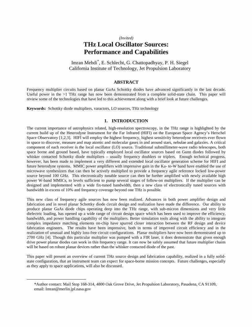
2.1. Power amplifier technology Given practical limitations on frequency conversion efficiencies and the high multiplication factor required to implement sources in the THz range when starting with pump sources near 100 GHz, a critical factor for upconversion is sufficient drive power. IMPATT and Gunn sources that have been used in previous submillimeter wave sources produce between 50 and 100 mW at 100 GHz and rapidly fall off in output power above this frequency. Power combining to enhance output power is possible, but difficult to stabilize. The electronic bandwidth of these sources is also extremely limited (typically a few hundred MHz) and can only be improved with mechanical tuners. The technology that has enabled power output of over 100 mW at 100 GHz with significant (>10%) electronic bandwidth are GaAs-based HEMT MMIC power amplifiers. Tremendous progress has been made on these devices in only a few short years, thanks in large part to high reliability MMIC fabrication processes that have been nurtured by the Department of Defense over the past twenty years. Figure 1 highlights the progress made on broadband MMIC power amplifiers over the last two decades. The right most data set is obtained from the modules that have been designed and built by a collaborative effort between JPL and TRW [7,8,9]. From a single module (with six MMICs) designed to cover the 92-106 GHz range, it is now possible to obtain in excess of 300 mW across the band at 120K. To further enhance performance, InP based HEMTs and high frequency HBTs are also being investigated [10]. A major task of the multiplier designers today is to harness this power with planar diode chips without burning them out.
Figure 1: Available output power from GaAs based MMIC power amplifier modules over the past 20 years. Early results were based on FET devices but with the advances in HEMT device technology operating frequencies at W-band (75-100 GHz) became possible. Recent progress has been mostly due to optimizing the device and circuit structures along with fabricating MMIC’s on much thinner substrates.
0.01
0.1
1
10
100
10 100 1000
Freq (GHz)
Pow
er (W
)
2002, GaAs HEMT, 120K
1999, GaAs HEMT
1998, GaAs HEMT
1995, GaAs HEMT
1980, GaAs FET
450 Frame ≈ 25 µm thick
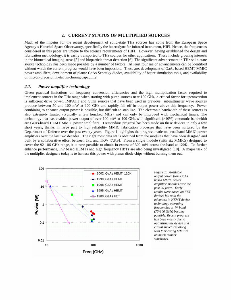
2.2. Advances in planar Schottky diode technology Whisker contacted Schottky varactor technology has been around for at least 40 years and has produced useable flight-qualified LO sources in the THz range [11]. However, there are some obvious limitations to this technology such as constraints on design, repeatability and reliability. The first high power planar Schottky diode varactor in the millimeter-wave range was demonstrated to great effect in 1993 by Erickson [12]. This design used a discrete multiple-diode chip soldered into a waveguide block. The technique works well into the 300 GHz range but at higher frequencies, where the waveguide size shrinks dramatically, it becomes difficult to implement due to tighter tolerance requirements. To improve the mechanical arrangement and reduce loss, a new “substrateless” technology was proposed in 1999 [13]. This novel circuit geometry was demonstrated upto 400 GHz a year later [14] and at 800 GHz in 2001 [15,16]. In this approach only a thin GaAs frame supports the planar diodes. Free standing metal lines and pads are used to create the matching circuitry, input and output coupling elements, DC interconnects and chip-to-waveguide block support structure. All elements of the chip are fabricated monolithically on a wafer scale with chemical processing used to separate individual circuits (no wafer dicing required). An example of such a circuit realizing a 200-to-400 GHz balanced doubler chip mounted in a waveguide block, is shown in Figure 2. This chip has two series anodes per branch (4 total) in order to greatly increase the input power handling capacity, and the design calls for a 22 micron thick substrate. A 400-to-800 GHz doubler of the a similar design requires a frame thickness of 12 microns and only one anode per branch is required due to the decrease in available input power at 400 GHz. These “drop-in” chips (clamped integrated beam leads form both electrical contact and physical support in the waveguide block – no soldering is required) make the assembly process very quick and straightforward and most importantly, repeatable. The beam leads further serve to make handling easier, provide both the DC and RF returns, and act as a low impedance path for removing heat from the diodes. The devices are placed anode-side-up in the split-waveguide block making it easy to visually inspect them – essential for space flight reliability screening. The anode sizes and critical dimensions for this circuit realization are limited to about 1.5 microns since a stepper aligner is used for most of the masking steps. It should be pointed out that a different substrate removal approach has been developed at the University of Virginia that utilizes a quartz host wafer. This technology has been demonstrated up to a few hundred GHz for mixer diodes [17] and work is continuing to extend it further for multiplier applications [18].
Figure 2: Photo of a 400 GHz doubler chip made with the substrateless technology mounted in a split-block waveguide. The diodes are placed in the input guide (left side) while the output guide is towards the right side of the picture. An on-chip capacitor is used to block RF power from flowing into the bias line. There is no GaAs under the matching circuit. Beam leads are used to place the chip and provide electrical contact to the block and bias line. Similar technology has been used to make chips at 200, 400 and 800 GHz.

The “substrateless” technology has proven to be very robust. A major early concern was the sensitivity of the multiplier performance to the substrate thickness. Since the GaAs wafers are prethinned via a chemical/mechanical process, the
tolerance on the thickness is hard to keep below +/- 5 microns. For the 200 GHz designs the nominal substrate thickness is 40 microns. However, simulations done with substrate thickness ranging from 30 to 50 microns indicate that only the input match is perturbed and this can be rectified to a certain extent by changing the diode capacitance (DC bias point). Finally, in order to push these devices to even higher operating frequencies, i.e. one THz and beyond, “membrane” diodes were proposed in 1999 [19] and first demonstrated by 2001 [20]. The unique feature of these devices is that all of the non-epitaxially grown semi-insulating GaAs substrate is removed and the entire circuit is fabricated on the remaining three-micron thick epitaxially grown semi-insulating GaAs membrane. Similar technology was successfully demonstrated earlier for a 2.5 THz Schottky diode mixer on the Earth Observing System Microwave Limb Sounder (EOS-MLS) [21]. The anode sizes and critical dimensions for this circuit realization are submicron since e-beam direct write lithography is used for processing. The fabrication steps used for these devices have been detailed in [22] and a nominal 1500 GHz balanced doubler chip is shown in Figure 3. Membrane technology is more complicated to implement but necessary, given the requirements for high frequency operation. For a successful design at 1200 GHz one of the most critical dimensions is the anode size. Even though the anodes are e-beam written, given the number of difficult fabrication steps preceding the write and the inherent tolerance on the e-beam writing procedure, some variation in nominal area can be expected. To minimize the impact of this variation the mask set includes a plus/minus variation of 15% on the anode size. Simulation results showing the effect of anode size on expected multiplier performance at 1200 GHz are shown in Figure 4.
30
40
50
60
70
80
1100 1125 1150 1175 1200 1225 1250 1275
Freq (GHz)
Out
put P
ower
(mic
row
att)
0.85fF(0.4x0.7) 1.06fF (0.4x0.9)1.28fF (0.4x1.1)
Figure 4: Simulated output power of a 1200 GHztripler for three different anode sizes at roomtemperature. Input power of 7 mW is assumed. Thechip is designed for zero bias. The nominal anode(1.06 fF) provides the optimum frequency coverage,however the surrounding circuit design allows forsome variation in the anode size without dramaticimpact on overall performance. The required designspecification for HIFI was to obtain 30-40 microwattsfrom 1120 to 1250 GHz when operating at an ambienttemperature of 120K.
Figure 3: SEM photograph of the anode area for a balanced 1500 GHz doubler chip. Beam-leads provide for grounding while a thicker GaAs frame (not shown here) is used to handle and position the chip in the waveguide block. Further details can be found in Erickson [24].

1.E-03
1.E-02
1.E-01
1.E+00
1.E+01
1.E+02
1.E+02 1.E+03 1.E+04
Freq (GHz)
Pow
er (m
W)
X2x2x2x2x2x2x2x2x3x2x2x2x2
Figure 5: Recent performance from planar all-solid-state sources at room temperature. The dashed line indicates the 1/f 2 roll off. All chains are pumped with 150-200 mW of input power from HEMT based power amplifier modules.
1.E-01
1.E+00
1.E+01
1.E+02
1.E+02 1.E+03 1.E+04
Freq (GHz)
Effic
ienc
y (%
)
2.3. Multiplier performance Planar devices built at JPL have been used to build solid-state LO chains up to 1500 GHz. Key results obtained thus far from work performed at JPL, University of Massachusetts, and Radiometer Physics (GmbH) are complied in Figure 5. Nominally the first stage doubler is pumped with 150-200 mW. The fix-tuned 3dB bandwidth is approximately 10%. This multiplier is then used to pump a second stage doubler. The fix tuned 10% bandwidth is still obtainable at the higher frequency. This two-stage chain is now used to drive higher frequency doublers and triplers. A doubler to 800 GHz has produced in excess of 1 mW at room temperature [16]. A tripler to 1200 GHz has produced about 70-100 µW at room temperature with a 5% 3dB bandwidth [23]. Finally, an 800 GHz chain (x2x2x2) has been used to pump a 4th stage doubler to 1600 GHz. At room temperature peak powers of 9 µW have been measured. When the entire chain is cooled to 70K, this output power increases to a very impressive 45 µW [24]. This chain has been used to successfully pump hot electron bolometer (HEB) mixers in this frequency range.
3. FUTURE CHALLENGES Despite recent successes with this technology there continue to be areas that can be improved. In large part, the desired improvements will be governed by the requirements of future space flight missions. However, higher output power and increased bandwidth are valuable to almost all application areas.
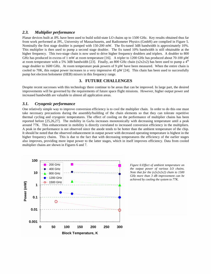
3.1. Cryogenic performance One relatively simple way to improve conversion efficiency is to cool the multiplier chain. In order to do this one must take necessary precautions during the assembly/building of the chain elements so that they can tolerate repetitive thermal cycling and cryogenic temperatures. The effect of cooling on the performance of multiplier chains has been reported before [25,26,27]. The mobility in GaAs increases monotonically with decreasing temperature until a peak around 77K. This enhancement in mobility is directly correlated to increased conversion efficiency in the multipliers. A peak in the performance is not observed since the anode tends to be hotter than the ambient temperature of the chip. It should be noted that the observed enhancement in output power with decreased operating temperature is highest in the higher frequency chains. This is due to the fact that with decreasing temperatures the efficiency of the earlier stages also improves, providing more input power to the latter stages, which in itself improves efficiency. Data from cooled multiplier chains are shown in Figures 6 and 7.
Figure 6:Effect of ambient temperature on the output power of various LO chains. Note that for the (x2x2x2x2) chain to 1500 GHz more than 3 dB improvement can be achieved by cooling the system to 77K.
0.001
0.01
0.1
1
10
100
0 50 100 150 200 250 300Block Temperature, K
Pow
er (m
W)
200 GHz400 GHz800 GHz1200 GHz1500 GHz

1.E-03
1.E-02
1.E-01
1.E+00
1.E+01
1.E+02
1.E+02 1.E+03 1.E+04
Freq (GHz)
Pow
er (m
W)
X2x2x2x2x2x2x2x2x3x2x2x2x2x2x3x2x2x3x3
120K
1.E-01
1.E+00
1.E+01
1.E+02
1.E+02 1.E+03 1.E+04
Freq (GHz)
Effic
ienc
y (%
)
Figure 7: Performance of recently tested all-solid-state LO sources at 120 K. All of these chains are built with planar Schottky diodes and are pumped with power amplifier modules. Nominally 150-200 mW of input power at w-band is used.
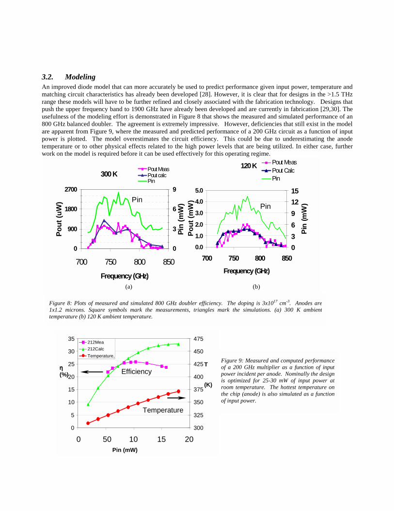
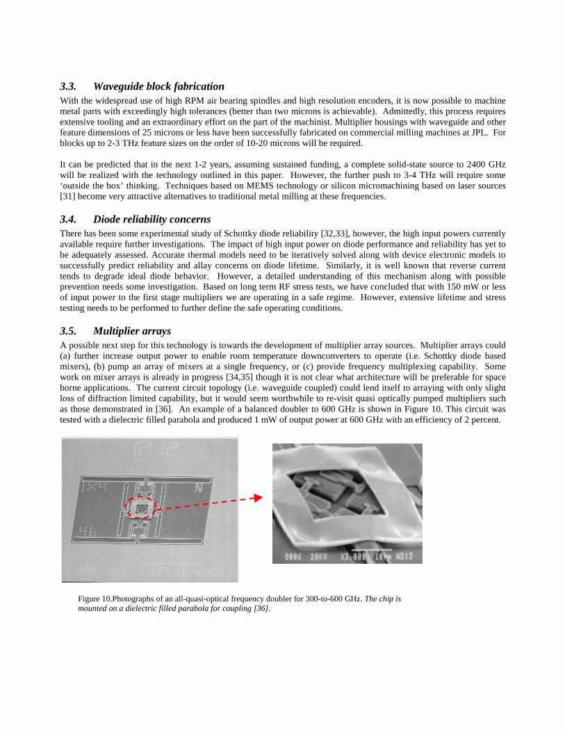
3.2. Modeling An improved diode model that can more accurately be used to predict performance given input power, temperature and matching circuit characteristics has already been developed [28]. However, it is clear that for designs in the >1.5 THz range these models will have to be further refined and closely associated with the fabrication technology. Designs that push the upper frequency band to 1900 GHz have already been developed and are currently in fabrication [29,30]. The usefulness of the modeling effort is demonstrated in Figure 8 that shows the measured and simulated performance of an 800 GHz balanced doubler. The agreement is extremely impressive. However, deficiencies that still exist in the model are apparent from Figure 9, where the measured and predicted performance of a 200 GHz circuit as a function of input power is plotted. The model overestimates the circuit efficiency. This could be due to underestimating the anode temperature or to other physical effects related to the high power levels that are being utilized. In either case, further work on the model is required before it can be used effectively for this operating regime.
300 K
0
900
1800
2700
700 750 800 850Frequency (GHz)
Pout
(uW
)
0
3
6
9Pi
n (m
W)
Pout MeasPout calcPin
Pin
120 K
0.01.0
2.0
3.0
4.05.0
700 750 800 850
Frequency (GHz)
Pout
(mW
)
03691215
Pin
(mW
)
Pout MeasPout CalcPin
Pin
(a) (b)
Figure 8: Plots of measured and simulated 800 GHz doubler efficiency. The doping is 3x1017 cm-3. Anodes are1x1.2 microns. Square symbols mark the measurements, triangles mark the simulations. (a) 300 K ambienttemperature (b) 120 K ambient temperature.
0 5
10 15 20 25 30 35
0 50 10 15 20Pin (mW)
ηηηη (%)
300
325
350
375
400
425
450
475
T (K)
212Mea212Calc Temperature,
Temperature
Efficiency Figure 9: Measured and computed performance of a 200 GHz multiplier as a function of input power incident per anode. Nominally the design is optimized for 25-30 mW of input power at room temperature. The hottest temperature on the chip (anode) is also simulated as a function of input power.
3.3. Waveguide block fabrication With the widespread use of high RPM air bearing spindles and high resolution encoders, it is now possible to machine metal parts with exceedingly high tolerances (better than two microns is achievable). Admittedly, this process requires extensive tooling and an extraordinary effort on the part of the machinist. Multiplier housings with waveguide and other feature dimensions of 25 microns or less have been successfully fabricated on commercial milling machines at JPL. For blocks up to 2-3 THz feature sizes on the order of 10-20 microns will be required. It can be predicted that in the next 1-2 years, assuming sustained funding, a complete solid-state source to 2400 GHz will be realized with the technology outlined in this paper. However, the further push to 3-4 THz will require some ‘outside the box’ thinking. Techniques based on MEMS technology or silicon micromachining based on laser sources [31] become very attractive alternatives to traditional metal milling at these frequencies.
3.4. Diode reliability concerns There has been some experimental study of Schottky diode reliability [32,33], however, the high input powers currently available require further investigations. The impact of high input power on diode performance and reliability has yet to be adequately assessed. Accurate thermal models need to be iteratively solved along with device electronic models to successfully predict reliability and allay concerns on diode lifetime. Similarly, it is well known that reverse current tends to degrade ideal diode behavior. However, a detailed understanding of this mechanism along with possible prevention needs some investigation. Based on long term RF stress tests, we have concluded that with 150 mW or less of input power to the first stage multipliers we are operating in a safe regime. However, extensive lifetime and stress testing needs to be performed to further define the safe operating conditions.
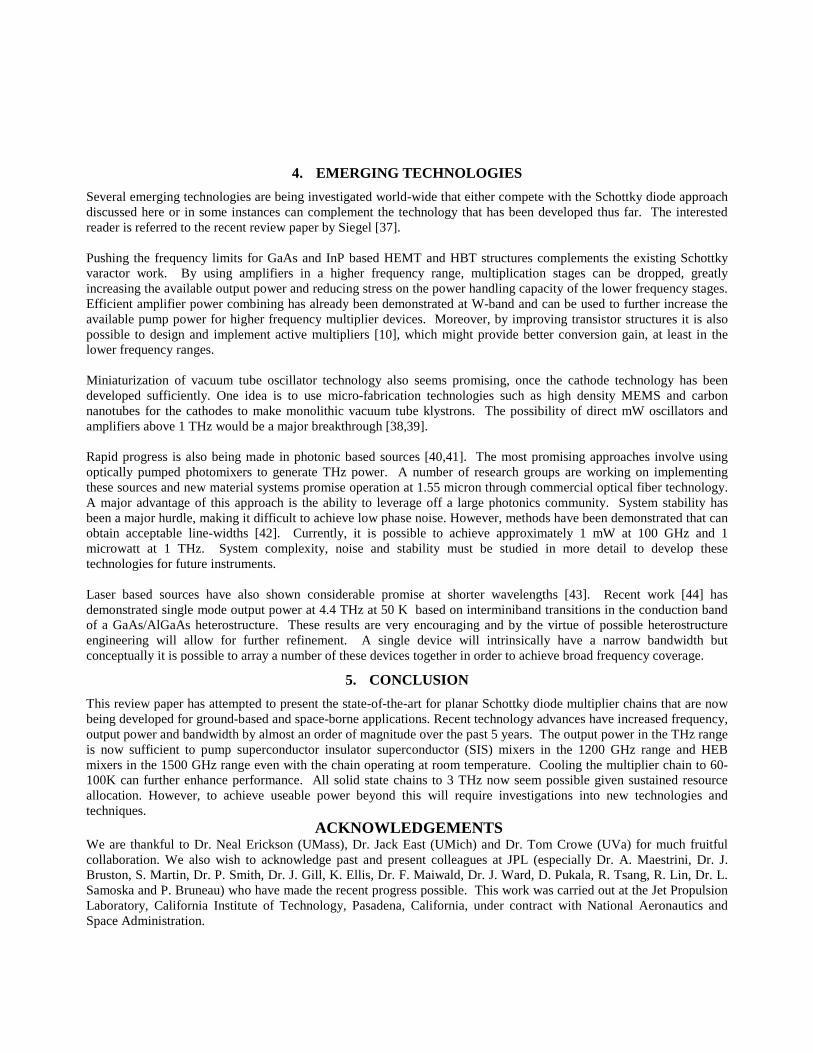
3.5. Multiplier arrays A possible next step for this technology is towards the development of multiplier array sources. Multiplier arrays could (a) further increase output power to enable room temperature downconverters to operate (i.e. Schottky diode based mixers), (b) pump an array of mixers at a single frequency, or (c) provide frequency multiplexing capability. Some work on mixer arrays is already in progress [34,35] though it is not clear what architecture will be preferable for space borne applications. The current circuit topology (i.e. waveguide coupled) could lend itself to arraying with only slight loss of diffraction limited capability, but it would seem worthwhile to re-visit quasi optically pumped multipliers such as those demonstrated in [36]. An example of a balanced doubler to 600 GHz is shown in Figure 10. This circuit was tested with a dielectric filled parabola and produced 1 mW of output power at 600 GHz with an efficiency of 2 percent. Figure 10.Photographs of an all-quasi-optical frequency doubler for 300-to-600 GHz. The chip is
mounted on a dielectric filled parabola for coupling [36].
4. EMERGING TECHNOLOGIES Several emerging technologies are being investigated world-wide that either compete with the Schottky diode approach discussed here or in some instances can complement the technology that has been developed thus far. The interested reader is referred to the recent review paper by Siegel [37]. Pushing the frequency limits for GaAs and InP based HEMT and HBT structures complements the existing Schottky varactor work. By using amplifiers in a higher frequency range, multiplication stages can be dropped, greatly increasing the available output power and reducing stress on the power handling capacity of the lower frequency stages. Efficient amplifier power combining has already been demonstrated at W-band and can be used to further increase the available pump power for higher frequency multiplier devices. Moreover, by improving transistor structures it is also possible to design and implement active multipliers [10], which might provide better conversion gain, at least in the lower frequency ranges. Miniaturization of vacuum tube oscillator technology also seems promising, once the cathode technology has been developed sufficiently. One idea is to use micro-fabrication technologies such as high density MEMS and carbon nanotubes for the cathodes to make monolithic vacuum tube klystrons. The possibility of direct mW oscillators and amplifiers above 1 THz would be a major breakthrough [38,39]. Rapid progress is also being made in photonic based sources [40,41]. The most promising approaches involve using optically pumped photomixers to generate THz power. A number of research groups are working on implementing these sources and new material systems promise operation at 1.55 micron through commercial optical fiber technology. A major advantage of this approach is the ability to leverage off a large photonics community. System stability has been a major hurdle, making it difficult to achieve low phase noise. However, methods have been demonstrated that can obtain acceptable line-widths [42]. Currently, it is possible to achieve approximately 1 mW at 100 GHz and 1 microwatt at 1 THz. System complexity, noise and stability must be studied in more detail to develop these technologies for future instruments. Laser based sources have also shown considerable promise at shorter wavelengths [43]. Recent work [44] has demonstrated single mode output power at 4.4 THz at 50 K based on interminiband transitions in the conduction band of a GaAs/AlGaAs heterostructure. These results are very encouraging and by the virtue of possible heterostructure engineering will allow for further refinement. A single device will intrinsically have a narrow bandwidth but conceptually it is possible to array a number of these devices together in order to achieve broad frequency coverage.
5. CONCLUSION This review paper has attempted to present the state-of-the-art for planar Schottky diode multiplier chains that are now being developed for ground-based and space-borne applications. Recent technology advances have increased frequency, output power and bandwidth by almost an order of magnitude over the past 5 years. The output power in the THz range is now sufficient to pump superconductor insulator superconductor (SIS) mixers in the 1200 GHz range and HEB mixers in the 1500 GHz range even with the chain operating at room temperature. Cooling the multiplier chain to 60-100K can further enhance performance. All solid state chains to 3 THz now seem possible given sustained resource allocation. However, to achieve useable power beyond this will require investigations into new technologies and techniques.
ACKNOWLEDGEMENTS We are thankful to Dr. Neal Erickson (UMass), Dr. Jack East (UMich) and Dr. Tom Crowe (UVa) for much fruitful collaboration. We also wish to acknowledge past and present colleagues at JPL (especially Dr. A. Maestrini, Dr. J. Bruston, S. Martin, Dr. P. Smith, Dr. J. Gill, K. Ellis, Dr. F. Maiwald, Dr. J. Ward, D. Pukala, R. Tsang, R. Lin, Dr. L. Samoska and P. Bruneau) who have made the recent progress possible. This work was carried out at the Jet Propulsion Laboratory, California Institute of Technology, Pasadena, California, under contract with National Aeronautics and Space Administration.
REFERENCES
1. E. F. van Dishoek and F. P. Helmich, “Scientific drivers for future high-resolution far-infrared spectroscopy in space,”
Proc. 30th ESLAB Symp., Submillimetre and Far-Infrared Space Instrumentation 1996, ed. E. J. Rolfe, ESA SP-388, pp. 3-12.
2. G. Pilbratt, “The FIRST mission,” Proc. ESA Symp., The Far Infrared and Submillimetre Universe 1997, ESA SP-401. 3. N. D. Whyborn, “The HIFI Heterodyne Instrument for FIRST: Capabilities and Performance,” Proc. ESA Symp, The Far
Infrared and Submillimetre Universe 1997, ESA SP-401. 4. F. Maiwald, S. Martin, J. Bruston, A. Maestrini, T. Crawford, P. H. Siegel, “Design and performance of a 2.7 THz
waveguide tripler,” Proceedings of the 12th International Symp. on Space Terahertz Technology, pp. 320-329, San Diego, February 2001.
5. P.H. Siegel, “Applications of Submillimeter-Wave Imaging to Medical Diagnostics,” NIH grant 1K25 EB00109-01, August 2002.
6. E.R. Brown and P.H. Siegel, “THz Differential Absorption Radar for Remote Detection of Bioparticles,” Army 02-T002 STTR, A023-0098, July 2002.
7. R. R. Ferber, et al., “W-Band Power Amplifier Development for the Herschel HIFI Instrument,” Proc. of SPIE vol. 4855, August 2002.
8. L. Samoska, et al., “MMIC Power Amplifiers as Local Oscillator Drivers for FIRST,” Proc. SPIE vol. 4013, pp. 275-284, 2000. 9. H. Wang, et al., “Power-Amplifier Modules Covering 70-113 GHz using MMICs, “ IEEE Trans. Microwave Theory and
Techniques, vol. 49, pp. 9-16, 2001. 10. Lorene Samoska, Vesna Radisic, Miro Micovic, Ming Hu, Paul Janke, Catherine Ngo, “InP MMIC chip set for power sources
covering 80-170 GHz,” Proceedings of the 12th International Symp. on Space Terahertz Technology, pp. 477-484, San Diego, February 2001.
11. P. Zimmerman, “Multipliers for THz Local Oscillators,” Proc. SPIE vol. 3357, pp. 152-158, 1998. 12. N. R. Erickson, B. J. Rizzi, T.W. Crowe, “A High Power Doubler for 174 GHz Using a Planar Diode Array,” Proceedings
of the 4th International Symposium on Space Terahertz Technology, pp. 287-296, Los Angeles, March 1993. 13. I. Mehdi, E. Schlecht, A. Arzumanyan, J. Bruston, P. Siegel, R. Peter Smith, J. Pearson, S. Martin and D. Porterfield, “Development
of millimeter and submillimeter-wave local oscillator circuits for a space telescope,” Proc. SPIE, vol. 3795, pp. 329-337, Terahertz and Gigahertz Photonics, R.J. Hwu, K. Wu, Eds., October 1999.
14. E. Schlecht, J. Bruston, A. Maestrini, S. Martin, D. Pukala, R. Tsang, A. Fung, R. P. Smith , I. Mehdi, “200 And 400 GHz Schottky Diode Multipliers Fabricated with Integrated Air-Dielectric "Substrateless" circuitry,” Proc. Eleventh International Symposium on Space THz Technology, Ann Arbor, May 2000.
15. E. Schlecht, G. Chattopadhyay, A. Maestrini, A. Fung, S. Martin, D. Pukala, J. Bruston and I. Mehdi, “200, 400 and 800 GHz Schottky Diode “Substrateless” Multipliers: Design and Results,” IEEE Int. Microwave Symp. Digest, pp. 1649-1652, Phoenix, AZ, May 2001.
16. G. Chattopadhyay, E. Schlecht, J. Gill, S. Martin, A. Maestrini, D. Pukala, F. Maiwald, and I. Mehdi, “A Broadband 800 GHz Schottky Balanced Doubler,” IEEE Microwave Guided Wave Lett., vol. 12 no. 4, pp. 117-118, April 2002.
17. S. Marazita et al., IEEE Trans. On Electron Devices, Vol. 47, No. 6, June 2000. 18. T. Crowe, personnel communication. 19. J. Bruston, S. Martin, A. Maestrini, E. Schlecht, R.P. Smith, I. Mehdi, “The Frame-less Membrane: A Novel Technology for
THz Circuits,” Proc. Eleventh International Symposium on Space THz Technology, Ann Arbor, May 2000. 20. J. Bruston, A. Maestrini, D. Pukala, S. Martin, B. Nakamura, I. Mehdi, “A 1.2 THz Planar Tripler Using GaAs Membrane
Based Chips,” Proceedings of the 12th International Symp. on space Terahertz Technology, pp. 310-319, San Diego, February 2001.
21. P.H. Siegel, R.P. Smith, S. Martin and M. Gaidis, “2.5 THz GaAs Monolithic Membrane-Diode Mixer”, IEEE Transactions Microwave Theory and Techniques, vol. 47, no. 5, pp. 596-604, May 1999.
22. S. Martin, B. Nakamura, A. Fung, P. Smith, J. Bruston, A. Maestrini, F. Maiwald, P. Siegel, E. Schlecht and I. Mehdi, “Fabrication of 200 to 2700 GHz Multiplier Devices Using GaAs and Metal Membranes,” 2001 Int. Microwave Symp. Digest, pp. 1641-1644, Phoenix, AZ, May 2001.
23. Frank Maiwald, et al, “THz frequency multiplier chains based on planar Schottky diodes,” Proc. of SPIE vol. 4855, 2002. 24. N. Erickson, A. Maestrini, E. Schlecht, G. Chattopadhyay, J. Gill, and I. Mehdi, “1.5 THz all-Planar Multiplied Source,”
presented at the 13th International Symposium on Space THz Technology, Harvard, March 2002. 25. J. Louhi, A. Raisanen, and N. Erickson, “Cooled Schottky Varactor Frequency Multipliers at Submillimeter Wavelengths,”
IEEE Trans. On Microwave Theory and Techniques, Vol. 41, No. 4, April 1991, pp. 565-571. 26. A. Maestrini, D. Pukala, E. Schlecht, I. Mehdi, and N. Erickson, “Experimental investigation of local oscillator chains with
GaAs planar diodes at cryogenic temperatures,” Proceedings of the 12th International Symp. on space Terahertz Technology, pp. 495-503, San Diego, February 2001.
27. J. East and I. Mehdi, “Temperature Effects in Varactors and Multipliers,” Proceedings of the 12th International Symp. on Space Terahertz Technology, pp. 340-351, San Diego, February 2001.
28. E. Schlecht, G. Chattopadhyay, A. Maestrini, D. Pukala, J. Gill and I. Mehdi, “Harmonic Balance Optimization of Terahertz Schottky y diode Multipliers Using an advanced Device Model,” Proc. 13th Intl. Symp. on Space THz Tech., Boston, March, 2002.
29. A Maestrini, G. Chattopadhyay, E. Schlecht, and I. Mehdi, “1400-1900 GHz Membrane Based Schottky diode Triplers,” presented at the 13th International Symposium on Space THz Technology, Harvard, March 2002.
30. N. Erickson, personnel communications. 31. C. Drouet d’Aubigny, C. Walker, B. Jones, C. Groppi, J. Papapolymerou, and C. Tavernier, “Laser Micromachining
Fabrication of THz Components,” Proceedings of the 12th International Symp. on space Terahertz Technology, pp. 514-425, San Diego, February 2001.
32. M. Schubler, V. Krozer, J. H. Bock, M. Brandt, L. Vecci, R. Losi, and H. L. Hartnagel, “Pulsed stress reliability investigations of Schottky diodes and HBTs,” Microelectronics Reliability, Vol. 36, No. 11/12, pp. 1907-1910, 1996.
33. M. Brandt, M. Schubler, E. Parmeggiani, C. Lin, A. Simon, H. L. Hartnagel, “Thermal simulation and charactrisation of the reliability of THz Schottky diodes,” Microelectronics Reliability, Vol. 37, No. 10/11, pp. 1663-1666, 1997.
34. C. Walker, C. Groppi, A. Hungerford, C. Kulesa, D. Golish, , K. Jacobs, U. Graf, C. Martin, J. Kooi, “POLE STAR: An 810 GHz Array Receiver for AST/RO,” Proceedings of the 12th International Symp. on Space Terahertz Technology, pp. 540-552, San Diego, February 2001.
35. U. U. Graf, S. Heyminch, E. A Michael, S. Stanko, “KOSMA’S 490/810 GHz Array Receiver,” Proceedings of the 12th International Symp. on Space Terahertz Technology, pp. 553-562, San Diego, February 2001.
36. M. Kim, B. H. Fujuwara, D. A. Humphrey, S. C. Martin, R. P. Smith, and P. H. Siegel, “A 600 GHz Planar Frequency Multiplier Feed On a Silicon Dielectric-Filled Parabola,” Proc. of the 19th 1997 GaAs IC Symposium, pp. 287-290, Anaheim, Ca, October 1997.
37. P. Siegel, “THz Technology,” IEEE Transactions on MTT vol. 50, No. 3, March 2002. 38. P. Siegel, A. Fung, H. Manohara, J. Xu, and B. Chang, “Nanoklystron: A monolithic tube approach to THz power
generation,” Proc. of the Twelfth International Symposium on Space Terahertz Technology, pp. 81-90, San Diego, CA, February 2001.
39. J. East and G. Haddad, “Ballistic Tunneling Transit time devices for THz power generation,” Proc. of the Twelfth International Symposium on Space Terahertz Technology, pp. 62-72, San Diego, CA, February 2001.
40. T. Nguchi, A. Udea, H. Iwashita, S. Kakano, Y. Sekimoto, M. Ishiguro, T. Ishibashi, H. Ito, and T. Nagatuma, “Millimeter wave generation using a uni-travelling-carrier photodiode,” Proc. of the Twelfth International Symposium on Space Terahertz Technology, pp. 73-80, San Diego, CA, February 2001.
41. R. A. Wyss, et al., “Embedded Coplanar Strips Traveling-Wave Photomixers,” presented at the Twelfth International Symposium on Space Terahertz Technology, San Diego, CA, February 2001.
42. J. C. Pearson, P. Chen, H. M. Pickett, “Photomixer systems as submillimeter oscillators and coherent test sources,” Proceedings of SPIE conference 4855, August 2002.
43. C. Sirtori et al., Appl. Phys. Letts, Vol. 73, No. 24, pp. 3486-3488, Dec. 1998. 44. Rudeger Kohler, Alessandro Tredicucci, Fablo Beltram, Harvey E. Beere, Demund H. Linfield, A. Giles Davies, David A.
Ritchie, Rita C. Lotti, and Fausto Rossi, “Terahertz semiconductor-heterostructure laser,” Nature, Vol. 417, 9 May 2002.