Embed Size (px)
Citation preview

Prepared By: SANDEEP KUMAR K
ASSISTANT PROFESSOR
DEPARTMENT OF MECHATRONICS
ACHARYA INSTITUTE OF TECHNOLOGY
CHAPTER 3: THYRISTORS
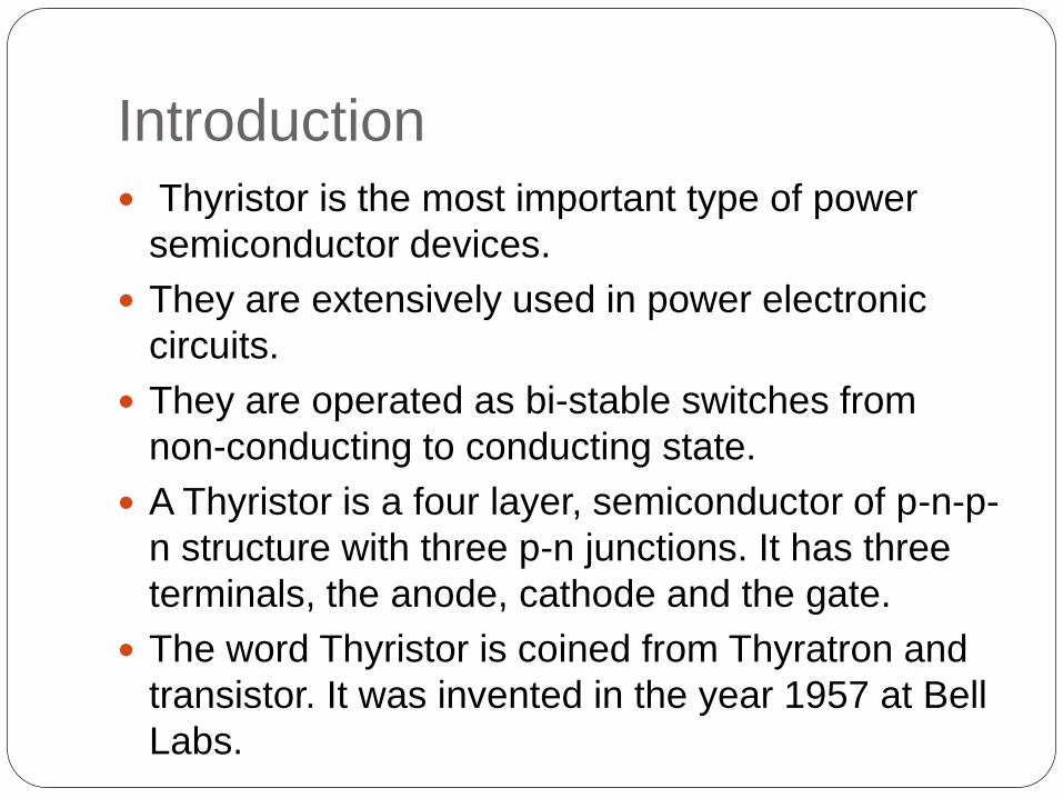
Introduction
Thyristor is the most important type of power
semiconductor devices.
They are extensively used in power electronic
circuits.
They are operated as bi-stable switches from
non-conducting to conducting state.
A Thyristor is a four layer, semiconductor of p-n-p-
n structure with three p-n junctions. It has three
terminals, the anode, cathode and the gate.
The word Thyristor is coined from Thyratron and
transistor. It was invented in the year 1957 at Bell
Labs.
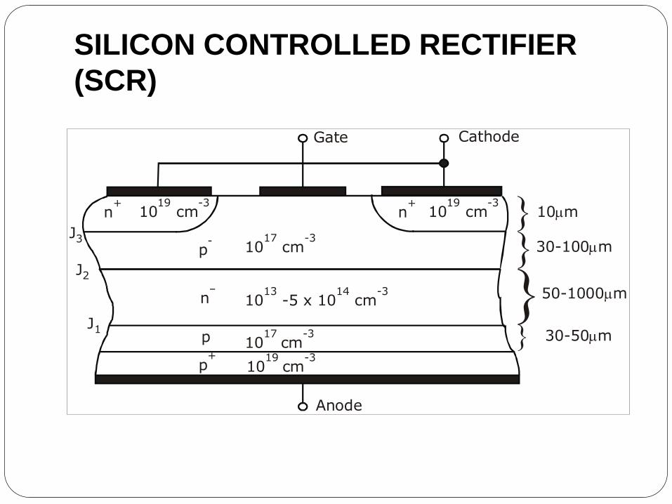
SILICON CONTROLLED RECTIFIER
(SCR)
Gate Cathode
J3
J2
J1
Anode
10 cm17 -3
10 -5 x 10 cm13 14 -3
10 cm17 -3
10 cm19 -3
10 cm19 -3
10 cm19 -3
n+
n+
p-
n–
p
p+
10 m
30-100 m
50-1000 m
30-50 m

QUALITATIVE ANALYSIS
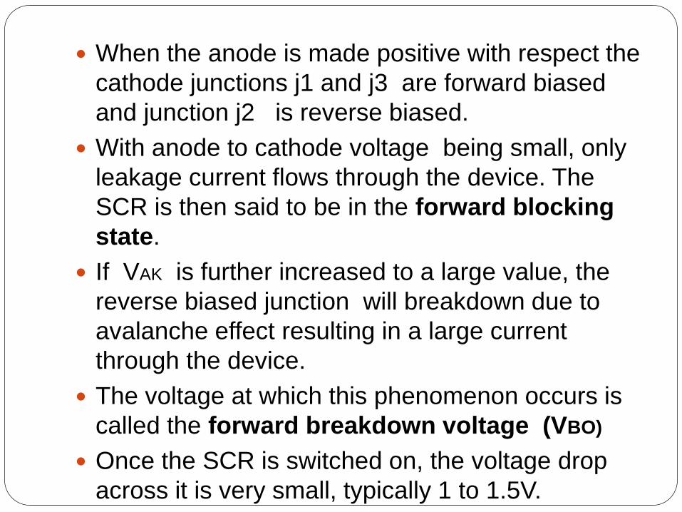
When the anode is made positive with respect the
cathode junctions j1 and j3 are forward biased
and junction j2 is reverse biased.
With anode to cathode voltage being small, only
leakage current flows through the device. The
SCR is then said to be in the forward blocking
state.
If VAK is further increased to a large value, the
reverse biased junction will breakdown due to
avalanche effect resulting in a large current
through the device.
The voltage at which this phenomenon occurs is
called the forward breakdown voltage (VBO)
Once the SCR is switched on, the voltage drop
across it is very small, typically 1 to 1.5V.

V-I Characteristics of SCR

Effects on gate current on forward
blocking voltage

LATCHING CURRENT (IL)
After the SCR has switched on, there is a
minimum current required to sustain conduction
even if the gate supply is removed. This current is
called the latching current. associated with turn
on and is usually greater than holding current.
HOLDING CURRENT (IH)
After an SCR has been switched to the on state
a certain minimum value of anode current is
required to maintain the Thyristor in ON state. If
the anode current is reduced below the critical
holding current value, the Thyristor cannot
maintain the current through it and turns OFF.

QUANTITATIVE ANALYSIS
TWO TRANSISTOR MODEL
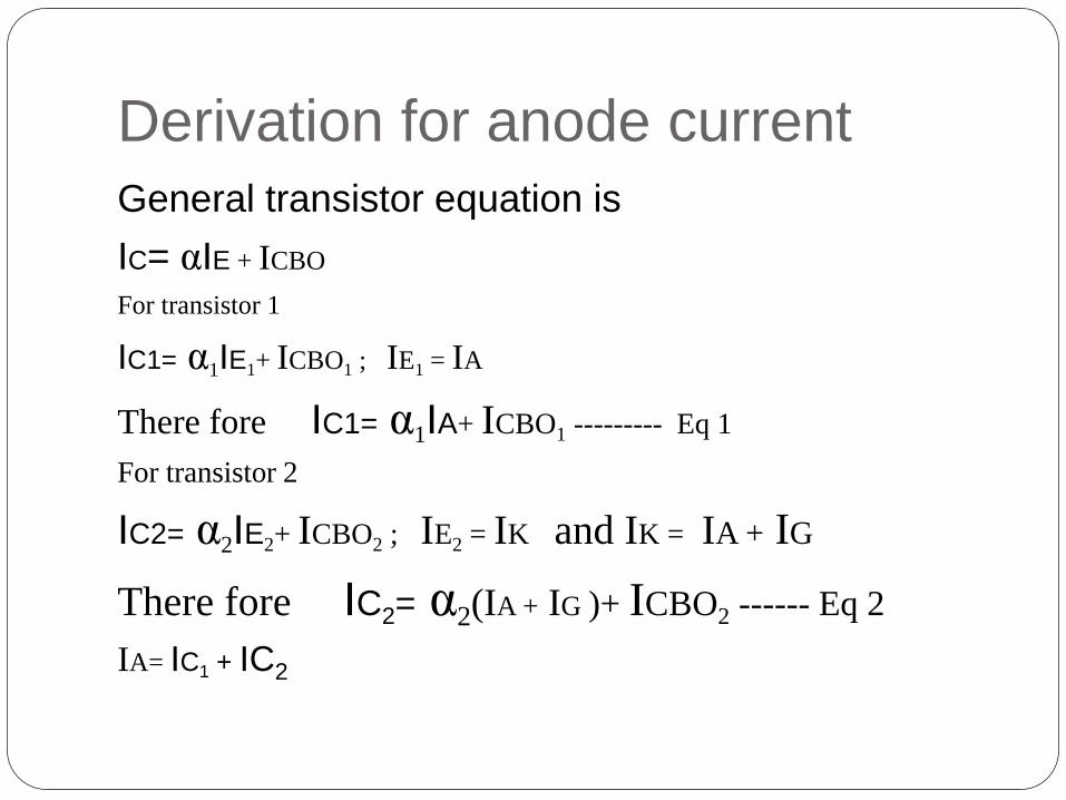
Derivation for anode current
General transistor equation is
IC= αIE + ICBO
For transistor 1
IC1= α1IE1+ ICBO1 ; IE1 = IA
There fore IC1= α1IA+ ICBO1 --------- Eq 1
For transistor 2
IC2= α2IE2+ ICBO2 ; IE2 = IK and IK = IA + IG
There fore IC2= α2(IA + IG )+ ICBO2 ------ Eq 2
IA= IC1 + IC2
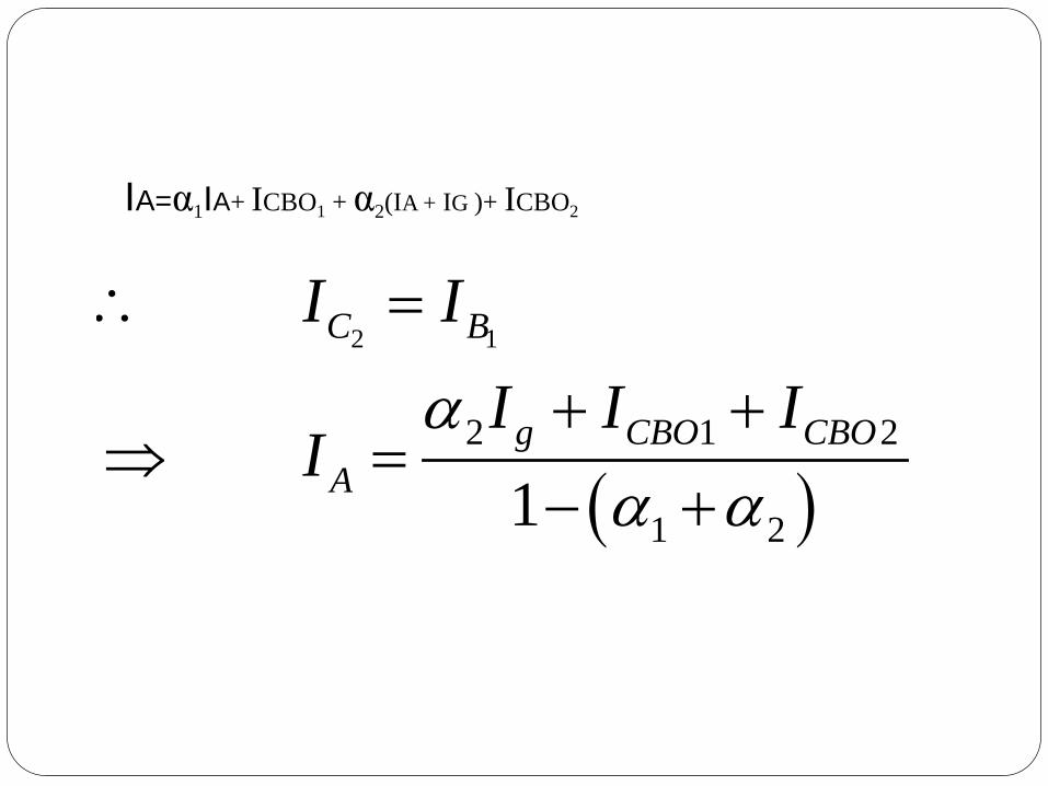
2 1
2 1 2
1 21
C B
g CBO CBO
A
I I
I I II
IA=α1IA+ ICBO1 + α2(IA + IG )+ ICBO2
THYRISTOR TURN ON
Thyristor is turned ON by increasing the Anode current,
this can be accomplished by one of the following ways
Thermal Turn on or High Temperature Triggering
Light Triggering
High Voltage Triggering
dv/dt Triggering
Gate Triggering
Thermal Turn on or High
Temperature
The width of depletion layer of SCR decreases
with increase in junction temperature.
Therefore in SCR when VAR is very near its
breakdown voltage, the device is triggered by
increasing the junction temperature.
By increasing the junction temperature the
reverse biased junction collapses thus the device
starts to conduct.
This type of turn on many cause thermal run
away and is usually avoided.

Light Triggering
For light triggered SCRs a special
terminal is made inside the inner P layer
instead of gate terminal.
When light is allowed to strike this
terminal, free charge carriers are
generated.
When intensity of light becomes more
than a normal value, the Thyristor starts
conducting.
This type of SCRs are called as LASCR
High Voltage Triggering
In this mode, an additional forward voltage is applied between anode and cathode.
When the anode terminal is positive with respect to cathode(VAK) , Junction J1 and J3 is forward biased and junction J2 is reverse biased.
No current flows due to depletion region in J2 is reverse biased (except leakage current).
As VAK is further increased, at a voltage VBO (Forward Break Over Voltage) the junction J2 undergoes avalanche breakdown and so a current flows and the device tends to turn ON(even when gate is open)
This type of turn on is destructive and should be avoided.
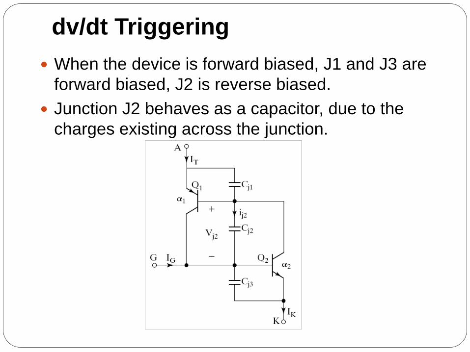
dv/dt Triggering
When the device is forward biased, J1 and J3 are
forward biased, J2 is reverse biased.
Junction J2 behaves as a capacitor, due to the
charges existing across the junction.
If voltage across the device is V, the charge by Q and capacitance by C then,ic = dQ/dtQ = CVic = d(CV) / dt
= C. dV/dt + V. dC/dtas dC/dt = 0
ic = C.dV/dt
Therefore when the rate of change of voltage across the device becomes large, the device may turn ON, even if the voltage across the device is small.
A high value of charging current may damage the Thyristor and the device must be protected against high .
The manufacturers will specify the allowable .

Gate Triggering
This is most widely used SCR triggering method.
Applying a positive voltage between gate and
cathode can Turn ON a forward biased Thyristor.
When a positive voltage is applied at the gate
terminal, charge carriers are injected in the inner
P-layer, thereby reducing the depletion layer
thickness.
As the applied voltage increases, the carrier
injection increases, therefore the voltage at which
forward break-over occurs decreases

Three types of signals are
used for gate triggering.
1. DC gate triggering
2. AC Gate Triggering
3. Pulse Gate Triggering

DC gate triggering
A DC voltage of proper polarity is applied between gate and cathode ( Gate terminal is positive with respect to Cathode).
When applied voltage is sufficient to produce the required gate Current, the device starts conducting.
One drawback of this scheme is that both power and control circuits are DC and there is no isolation between the two.
Another disadvantages is that a continuous DC signal has to be applied. So gate power loss is high.

AC Gate Triggering:-
Here AC source is used for gate
signals.
This scheme provides proper isolation
between power and control circuit.
Drawback of this scheme is that a
separate transformer is required to
step down ac supply.
There are two methods of AC voltage
triggering namely (i) R Triggering (ii)
RC triggering

3. Pulse Gate Triggering
In this method the gate drive consists of
a single pulse appearing periodically (or)
a sequence of high frequency pulses.
This is known as carrier frequency
gating.
A pulse transformer is used for
isolation.
The main advantage is that there is no
need of applying continuous signals, so
the gate losses are reduced.
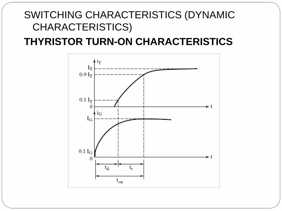
SWITCHING CHARACTERISTICS (DYNAMIC
CHARACTERISTICS)
THYRISTOR TURN-ON CHARACTERISTICS
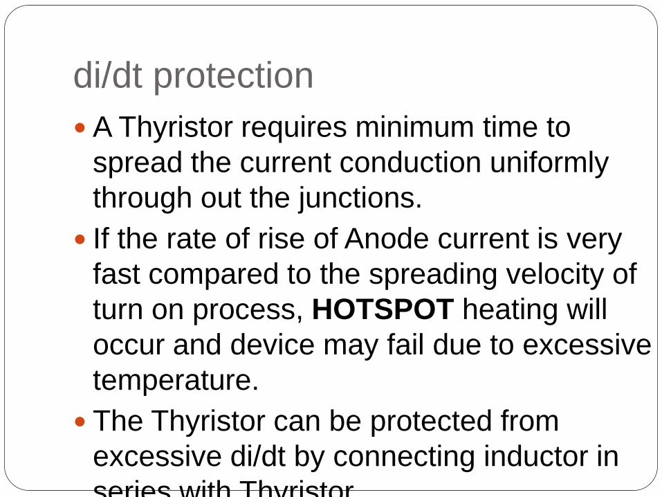
di/dt protection
A Thyristor requires minimum time to
spread the current conduction uniformly
through out the junctions.
If the rate of rise of Anode current is very
fast compared to the spreading velocity of
turn on process, HOTSPOT heating will
occur and device may fail due to excessive
temperature.
The Thyristor can be protected from
excessive di/dt by connecting inductor in
series with Thyristor.
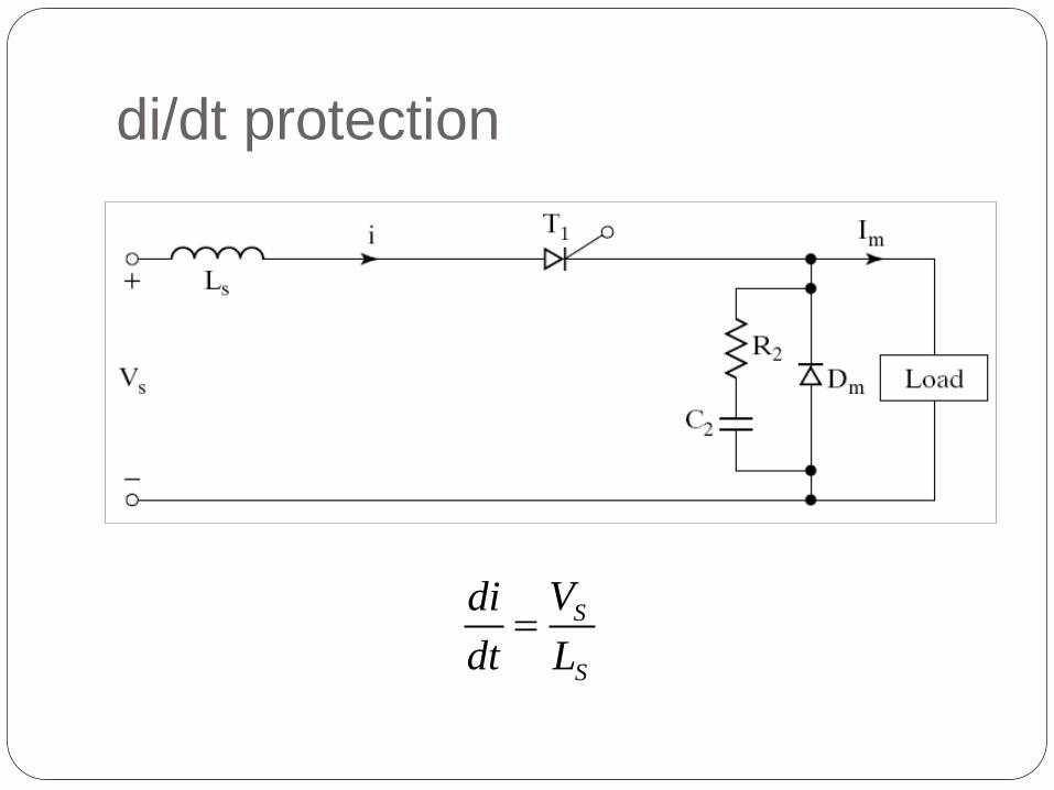
di/dt protection
S
S
Vdi
dt L
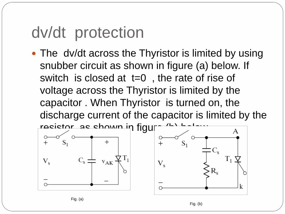
dv/dt protection
The dv/dt across the Thyristor is limited by using
snubber circuit as shown in figure (a) below. If
switch is closed at t=0 , the rate of rise of
voltage across the Thyristor is limited by the
capacitor . When Thyristor is turned on, the
discharge current of the capacitor is limited by the
resistor as shown in figure (b) below.
Fig. (a)
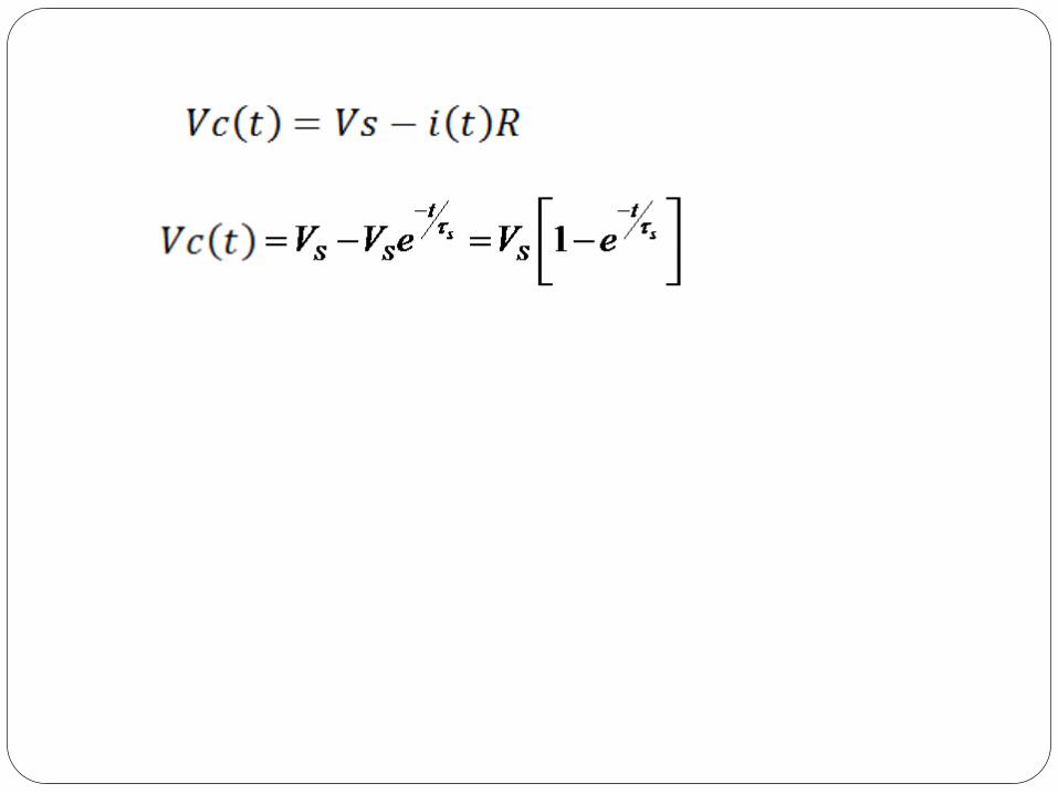
Fig. (b)

The voltage across the Thyristor will rise
exponentially as shown in fig above.
Assuming Vc(0)=0
t 0
10S S c for
V i t R i t dt VC

Now applying Laplace transform
OR
Now applying Inverse Laplace transform we get
s S SR C Where
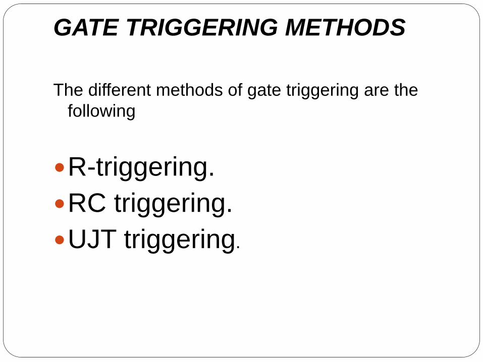
GATE TRIGGERING METHODS
The different methods of gate triggering are the
following
R-triggering.
RC triggering.
UJT triggering.

RESISTANCE TRIGGERING
LOAD
vO
a b
i R1
R2
D
R Vg
VT
v =V sin tS m
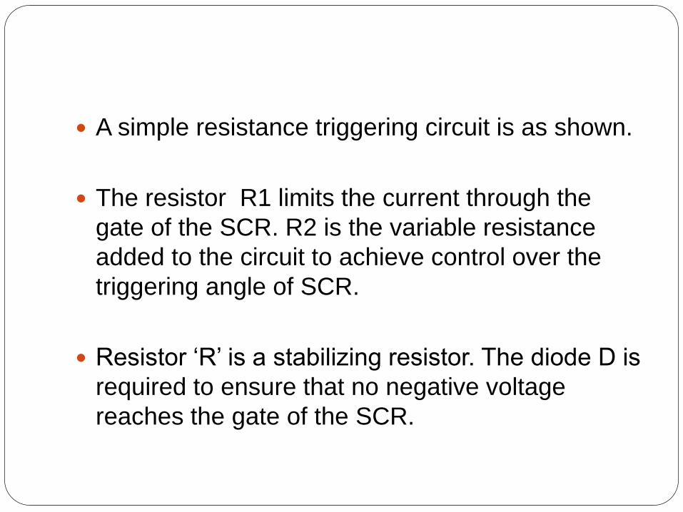
A simple resistance triggering circuit is as shown.
The resistor R1 limits the current through the
gate of the SCR. R2 is the variable resistance
added to the circuit to achieve control over the
triggering angle of SCR.
Resistor ‘R’ is a stabilizing resistor. The diode D is
required to ensure that no negative voltage
reaches the gate of the SCR.
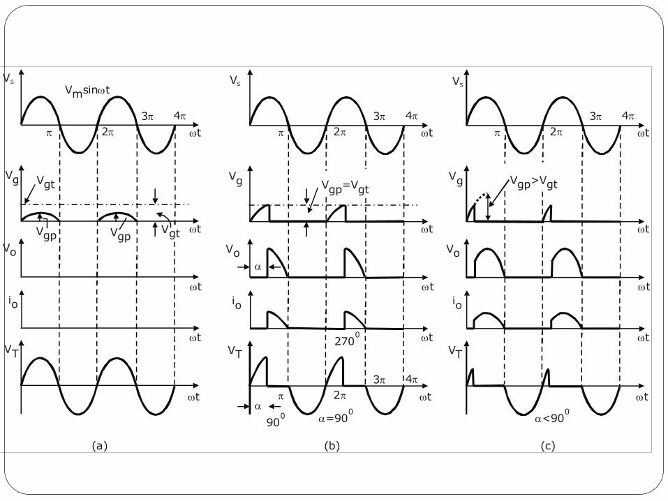
VS
2
3 4
t
V sin tm
Vg Vgt
t
t
t
t
Vo
io
VT
VgpVgtVgp
(a)
t
t
t
t
t
t
t
t
t
t
2
3 4
2
3 4
VS
Vg
Vo
io
VT
VS
Vg
Vo
io
VT
V =Vgp gt
2700
2
3 4
900 =90
0
(c)(b)
<900
V >Vgp gt

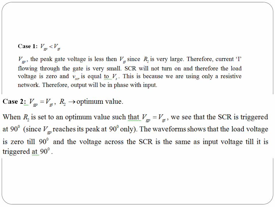
Design
With , R2=0 we need to ensure that , where
is the
maximum or peak gate current of the SCR.
Therefore
Also with , we need to ensure that the
voltage drop across resistor ‘R’ does not exceed ,
the maximum gate voltage
1
mgm
VI
R gmI
1m
gm
VR
I
2 0R
gmV
1
1
1
1
mgm
gm gm m
gm m gm
gm
m gm
V RV
R R
V R V R V R
V R R V V
V RR
V V


RESISTANCE CAPACITANCE
TRIGGERING
LOAD
vO
R
C
VT
v =V sin tS m
D2
VC
+
-D1
Capacitor ‘C’ in the circuit is connected to shift the
phase of the gate voltage.
Diode D1 is used to prevent negative voltage from
reaching the gate cathode of SCR.
In the negative half cycle, the capacitor charges to
the peak negative voltage of the supply (-Vm)
through the diode D2 .
The capacitor maintains this voltage across it, till
the supply voltage crosses zero. As the supply
becomes positive, the capacitor charges through
resistor ‘R’ from initial voltage of (-Vm) , to a
positive value.
When the capacitor voltage is equal to the gate
trigger voltage of the SCR, the SCR is fired and the
capacitor voltage is clamped to a small positive
value

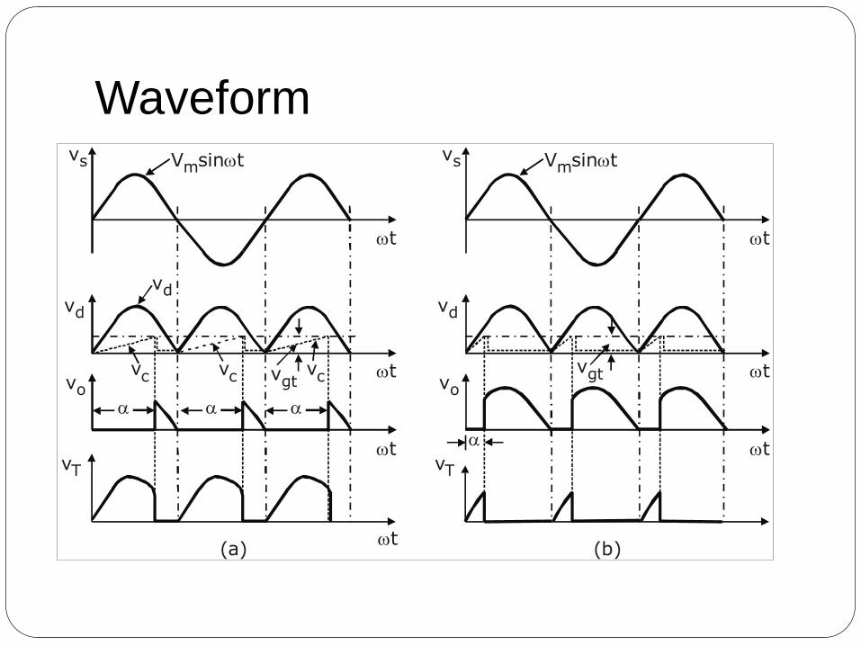
Waveform
vs
0
V sin tm
0 t
tt
avc
- /2
a
vc
Vgt
vo
vT
Vm
-Vm
vs
0
V sin tm
0t
avc
- /2
a
vc
Vgt
0
0
vo
vT
Vm Vm
-Vm(2 + )
(a) (b)
t t

Case 1: R Large.
When the resistor ‘R’ is large, the time taken for the capacitance to charge from (-Vm) to Vgt is large, resulting in larger firing angle and lower load voltage.
Case 2: R Small
When ‘R’ is set to a smaller value, the capacitor charges at a faster rate towards Vgt resulting in early triggering of SCR and hence VL is more.
When the SCR triggers, the voltage drop across it falls to 1 – 1.5V. This in turn lowers, the voltage across R & C. Low voltage across the SCR during conduction period keeps the capacitor discharge during the positive half cycle.

RC FULL WAVE
vO
R
C
VT
v =V sin tS m
+
-
LOAD+
-
D1 D3
D4 D2
vd
Waveform vs
vd
vo
vT
t
t
t
t
V sin tm
vd
vc vc vcvgt
V sin tm vs
vd
vo
vT
t
t
t
vgt
(a) (b)

UNI-JUNCTION TRANSISTOR (UJT)
RB2
VBB
+
-
E
B1
RB1VBB
A+
-
Ve Ie
B2
E
B2
B1B1
A
B2
E
RB2
RB1n-type
p-type
Eta-point
Eta-point
(a) (b) (c)

UJT is an n-type silicon bar in which p-type
emitter is embedded. It has three terminals
base1, base2 and emitter ‘E’.
Between B1 and B2 UJT behaves like ordinary
resistor and the internal resistances are given as
RB1 and RB2 with emitter open RBB=RB1+RB2 .
When VBB is applied across B1 and B2 , we find
that potential at A is
1 11
1 2 1 2
BB B BAB BB
B B B B
V R RV V
R R R R
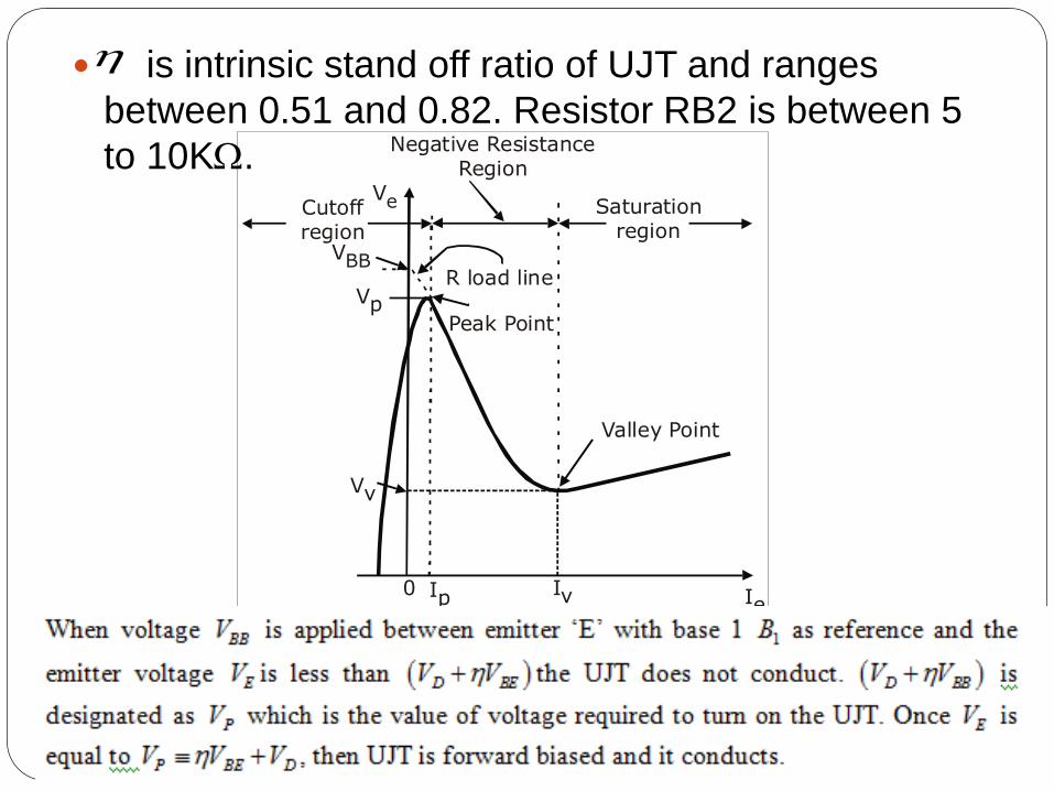
is intrinsic stand off ratio of UJT and ranges
between 0.51 and 0.82. Resistor RB2 is between 5
to 10K.
Ve
VBBR load line
Vp
Vv
IeIvIp0
Peak Point
Cutoffregion
Negative ResistanceRegion
Saturation region
Valley Point

UJT RELAXATION OSCILLATOR
UJT is highly efficient switch. The switching times
is in the range of nanoseconds. Since UJT
exhibits negative resistance characteristics it can
be used as relaxation oscillator.
The circuit diagram is as shown with R1 and R2
being small compared to RB1 and RB2 of UJT.
R R2
VBB
R1C
EB2
B1Ve vo
Ve
Vp
VV
Vo
t
t
Capacitorcharging
T =RC1
1
T
V +VBB
VP
T =R C2 1
Capacitordischarging
Vv
(a) (b)


SYNCHRONIZED UJT
OSCILLATOR
R
C
+
-
D1 D3
D4 D2
Vdc
R1
VZ
+
-
Z
i1
vc
+
-
R2
G1
C1
G2
C2
Pulse TransfE
B2
B1
To SCR
Gates
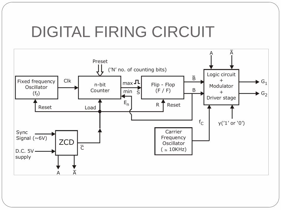
DIGITAL FIRING CIRCUIT
Fixed frequencyOscillator
(f )f
Logic circuit+
Modulator
+Driver stage
n-bitCounter
Flip - Flop(F / F)
Clk max
min S B
BG1
G2
A A
Reset LoadEn R Reset
ZCDD.C. 5V
supply
SyncSignal (~6V)
A A
C
CarrierFrequencyOscillator
( 10KHz)
fC y(’1’ or ‘0’)
Preset
(’N’ no. of counting bits)