Embed Size (px)
Citation preview
Threshold-Based Voltage Reference with pn- Junction Temperature Compensation
Yen-Ting WangDept. ofElectrical Engineering
Tatung University, [email protected]
Abstract
Randall L. GeigerDept. ofElectrical andComputer Engineering
Iowa State University, [email protected]
Shu-Chuan HuangDept. ofElectrical Engineering
Tatung University, [email protected]
V DD
A new voltage reference with output dependent uponthe threshold voltage of an NMOS transistor isintroduced. A low temperature coefficient is achievedby using a pn-junction PTAT current generator tocompensate for the negative temperature coefficient ofthe threshold voltage. Implemented in a standardO.6J1m CMOS process with an output of 1.67V, it has atemperature coefficient of 4.9ppmfC over a 195°Crange.
1. Introduction
Integrated voltage references with low sensitivity totemperature and supply voltage are a critical component inmany integrated circuits. Several methods of realizingreferences are discussed in [1]. All invariably use theweighted sum of two voltages, one with a positivetemperature coefficient and one with a negativetemperature coefficient, with the weight adjusted so thatthe thermal derivative vanishes at a predeterminedtemperature. The difference of two pn-junction voltagesis very linear in temperature and is actually proportional toabsolute temperature (PTAT). This difference is widelyused to generate the positive temperature coefficient (PTC)voltage. Correspondingly, the pn-junction voltage has anegative temperature coefficient (NTC) and is widely usedin references to generate the NTC voltage. Unfortunately,the pn-junction voltage does not vary linearly withtemperature and is the major contributor to the non zerotemperature coefficient (TC) of the reference. Manydifferent curvature-compensation techniques have beendeveloped to address this problem [4][5], but they are allbased on pn-junction type circuit. As an alternative,Manku [7] suggests using a single NMOS device toachieve a low TC reference and suggests a TC of 13ppmfrom O°C to 125 °C is achievable but gives no circuit.Filanovsky [8] demonstrated that diode-connectiontransistors can stabilize the current and voltage reference.
978-1-4244-4480-9/09/$25.00 ©2009 IEEE 156
Vss
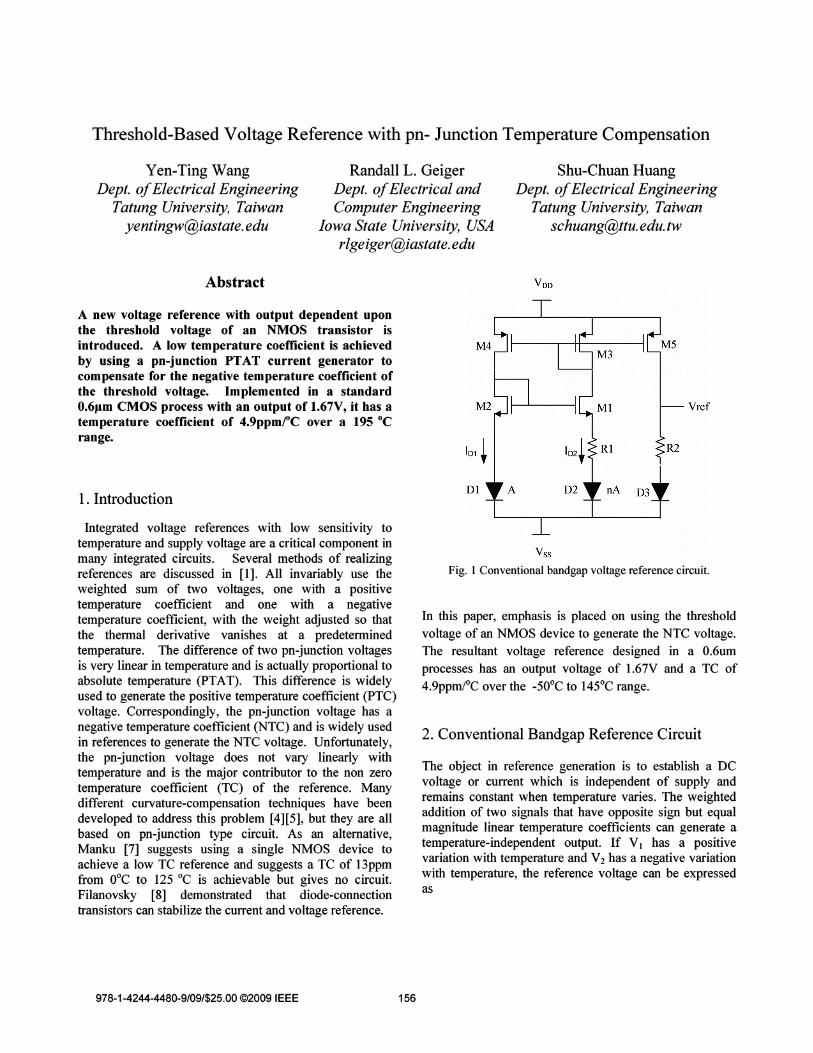
Fig. 1 Conventional bandgap voltage reference circuit.
In this paper, emphasis is placed on using the thresholdvoltage of an NMOS device to generate the NTC voltage.The resultant voltage reference designed in a O.6umprocesses has an output voltage of 1.67V and a TC of4.9ppmfC over the -50°C to 145°Crange.
2. Conventional Bandgap Reference Circuit
The object in reference generation is to establish a DCvoltage or current which is independent of supply andremains constant when temperature varies. The weightedaddition of two signals that have opposite sign but equalmagnitude linear temperature coefficients can generate atemperature-independent output. If V I has a positivevariation with temperature and V2 has a negative variationwith temperature, the reference voltage can be expressedas
v Vref v Vref
------------~~
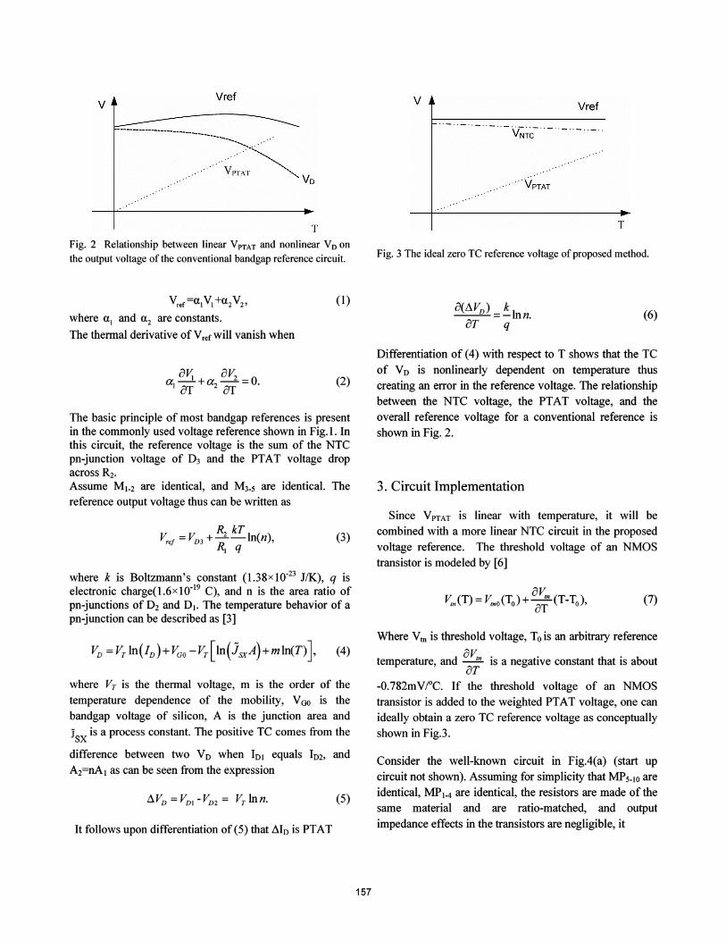
VPTAT '"'VD
'- "- "-\/~~C- '- " - " -" -"
.... .··· ··VPTAT
T
Fig. 2 Relationship between linear VPTAT and nonlinear VD onthe output voltage of the conventional bandgap reference circuit.
T
Fig. 3 The ideal zero TC reference voltage of proposed method.
Vref=0..V1+0.2V2,
where 0.1 and 0.2 are constants.
The thermal derivative of Vref will vanish when
(I)(6)
where k is Boltzmann's constant (1.38 x 10⁻²³ JIK), q iselectronic charget l .exlu" C), and n is the area ratio ofpn-junctions of D2 and DJ. The temperature behavior of apn-junction can be described as [3]
The basic principle of most bandgap references is presentin the commonly used voltage reference shown in Fig.I. Inthis circuit, the reference voltage is the sum of the NTCpn-junction voltage of D3 and the PTAT voltage dropacross R2•
Assume M._2 are identical, and M3-s are identical. Thereference output voltage thus can be written as
(7)
3. Circuit Implementation
Differentiation of (4) with respect to T shows that the TC
of VD is nonlinearly dependent on temperature thuscreating an error in the reference voltage. The relationshipbetween the NTC voltage, the PTAT voltage, and theoverall reference voltage for a conventional reference is
shown in Fig. 2.
Since VPTAT is linear with temperature, it will becombined with a more linear NTC circuit in the proposed
voltage reference. The threshold voltage of an NMOStransistor is modeled by [6]
(3)
(2)
s, kTVre/ = VD 3 +--In(n),
R. q
It follows upon differentiation of (5) that ~ID is PTAT
where Vr is the thermal voltage, m is the order of the
temperature dependence of the mobility, VGO is thebandgap voltage of silicon, A is the junction area and
isx is a process constant. The positive TC comes from the
difference between two VD when IDJ equals ID2, andA2=nA J as can be seen from the expression
(5)
Where VIn is threshold voltage, Tois an arbitrary reference
d av, . . h . btemperature, an __n IS a negative constant t at IS a outaT-O.782mV;oC. If the threshold voltage of an NMOStransistor is added to the weighted PTAT voltage, one canideally obtain a zero TC reference voltage as conceptually
shown in Fig.3 .
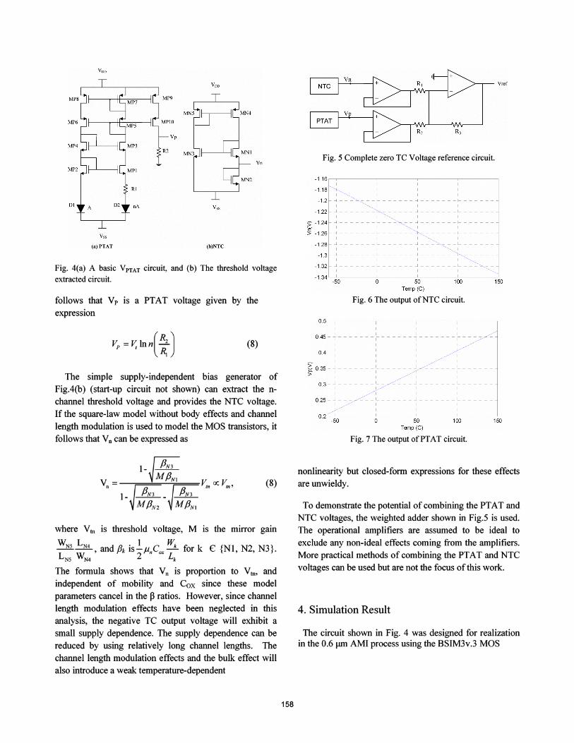
Consider the well-known circuit in Fig.4(a) (start up
circuit not shown). Assuming for simplicity that MPS-IO areidentical, MP J-4 are identical, the resistors are made of thesame material and are ratio-matched, and output
impedance effects in the transistors are negligible, it
157
VDn
v-er
150
+
R, R,
R,
-50 0 50 100Temp (C)
Fig. 6 The output ofNTC circuit.
Fig. 5 Complete zero TC Voltage reference circuit.
I I I
-------~------4-------~------
I I I I
-1.2 4--- ---~------4-------~------I I I I
4 4 ~ _
I I I I4 ~ 4 ~ _
I I I I4 ~______ _ ~ _
I I I I4 ~ J L _
I I I I-1.3 J L J ------
I I I IJ L J L _
I I I I
-1.18
-1.22
-1.28
-1.34 "---:'-::--- - ---'- - - -----='------ - -----,-'-::-- - -----,:
-1.32
:> -1.24c:> -1.26
- 1.16 ,---,----~----~---~--_____,
0.5 r-r---~---_____;~---~--_____,
Vn
Vss
(b)NTC
Vp
MP9
R2
Vss
(a) PTAT
follows that VP is a PTAT voltage given by theexpression
Fig. 4(a) A basic VPTA T circuit, and (b) The threshold voltageextracted circuit.
150
I_____ -1 _
I
I_ J L _
I II I
II------1-------I
-----_....!_-----II
______ J _
-50 0 50 100Temp (C)
Fig. 7 The output ofPTAT circuit.
0.2 L-L - - - ---'- - - -----.J'------ - - L-- - -----.J
I
I1-------I
0.4 ~ - - - - - - -I
J _II
0.3 -I - - - - - - I
I...1 _
I
0.45
0.25
~035>
(8)
The simple supply-independent bias generator ofFig.4(b) (start-up circuit not shown) can extract the nchannel threshold voltage and provides the NTC voltage.If the square-law model without body effects and channel
length modulation is used to model the MOS transistors, itfollows that V0 can be expressed as
(8)
where VIn is threshold voltage, M is the mirror gain
WN5 LN4, and 13k is'!",unCox Wk for k e {Nl, N2, N3} .
LN5 WN4 2 t;The formula shows that Vo is proportion to VIn , and
independent of mobility and Cox since these modelparameters cancel in the pratios . However, since channellength modulation effects have been neglected in thisanalysis, the negative TC output voltage will exhibit asmall supply dependence. The supply dependence can bereduced by using relatively long channel lengths. Thechannel length modulation effects and the bulk effect willalso introduce a weak temperature-dependent
nonlinearity but closed-form expressions for these effectsare unwieldy.
To demonstrate the potential of combining the PTAT andNTC voltages, the weighted adder shown in Fig.5 is used.The operational amplifiers are assumed to be ideal toexclude any non-ideal effects coming from the amplifiers.
More practical methods of combining the PTAT and NTCvoltages can be used but are not the focus of this work.
4. Simulation Result
The circuit shown in Fig. 4 was designed for realizationin the 0.6 IlIl1 AMI process using the BSIM3v.3 MOS
158
1.6695 ,---,-- - - -----,- - - ----,-- - - ---,-- - - ---,
Table I TC ofVn and Vp and weighted resistors in the addingcircuit.
1.669
1.6685>W> 1.668
1.6675
II
I I I-------,------1-- ----I
I I II I
I I I II ------1----- ,-------1------I I I II I I I
J ~ J ~ _I I I II I I II I I I~ L ~ L _I I I II I I II I I I
Voltage TC Weighted ResistorVn -7.82xlO-4 Rl I IKQVp 1.25x10⁻³ R2=R3 I 1.6KQ
Table 2 Comparison of recent works.
Temperature range TCThis work -SO°C-14S°C(190°C) 4.91ppm
r71199S 0°C-12S0C(12S0C) 13ppm[812000 -SO°C-lS0°C(200°C) 31.3ppm[912004 -SO°C-lS0°C(200°C) 4ppm
Conventional 190°C 8.32ppm[Fig. 9]
6. References
1.667 '------:'-,------ - -----'--- - - ---::':-- - - ---L..- - - ---'-50 0 50 100 150
Temp (C)
Fig.8 Reference voltage simulate from -50°C to 145°C.
model. The TC parameters and resistor values used in thesimulation are shown in Table l. Fig. 6 and Fig. 7 showthe simulation results for Vn and Vp. Fig. 8 shows theoverall reference voltage Vref. Vref is 1.668V at 27°C andthe TC is 4.91ppmrC from -50°C to 145°C. It can be seenthat there are two inflection points which are due to theweak nonlinearities in the NTC.
Table. 2 shows the comparison between different works[7][8][9]. When compared with the conventional bandgapcircuit result shown in Fig. 9, the new reference provides areduction in the TC of nearly a factor of 2.
5. Conclusion
A new approach for designing a voltage reference using apn-junction based PTAT source and an n-channel VIbasedNTC source was introduced. Simulation results show thenew circuit has a TC equals of 4.91ppmrC from -50°C to145°C which is nearly a factor of 2 less than that of astandard bandgap reference .
TC of the conventional Bandgap Reference10 (+1- ppm/C)
8
6U1-4
2
o
(1) B. Razavi, Design of Analog CMOS Integrated Circuits,McGraw-Hill, 2000.[2] RJ. Widlar, "New developments in IC voltage regulators,"IEEE J. Solid-State Circuits, voI.SC-6, no.I , pp.2-7, Feb. 1971.[3] X. Dai, D. Chen and R.L. Geiger, "Explicit Characterizationof Bandgap References", IEEE International Symposium onCircuits and Systems, pp. 573-576, May 2006.[4] B.S. Song, P.R. Gray, "Precision Curvature-CompensatedCMOS Bandgap Reference" IEEE J.Solid-State Circuits, vol.SC18, no.6, Dec. 1983.[5] L M. Filanovsky, A. Allam, "Mutual Compensation ofMobility and Threshold Voltage Temperature Effects withApplications in CMOS Circuits", IEEE Trans. Circuits andSystems-s-I: FUNDAMENTAL THEORY AND APPLICATIONS,VOL. 48, NO.7, Jul. 2001[6] Y.P. Tsividis, Operation and Modeling of the MOSTransistor, New York: McGraw-Hill, 1987.[7] T. Manku and Y. Wang, "Temperature-independent outputvoltage generated by threshold voltage of an NMOS transistor,"Electron. Lett., vol.3l , no. 6, pp. 935-936, 1995.[8] LM. Filanovsky, T.L. Su, "Interaction of threshold voltageand mobility temperature dependencies applied to stabilization ofcurrent and voltage," Circuits and Systems, 2000. Proceedings ofthe 43rd IEEE Midwest Symposium on , vol.3, no., pp.l 022-1025vol.3, 2000.[9] L. Najafizadeh, and LM. Filanovsky, "A simple voltagereference using transistor with ZTC point and PTAT currentsource," IEEE International Symposium on Circuits and Systems,May 2004, Vol. 1, pp.909-911.
o 50 100 150 200
Temperature Range
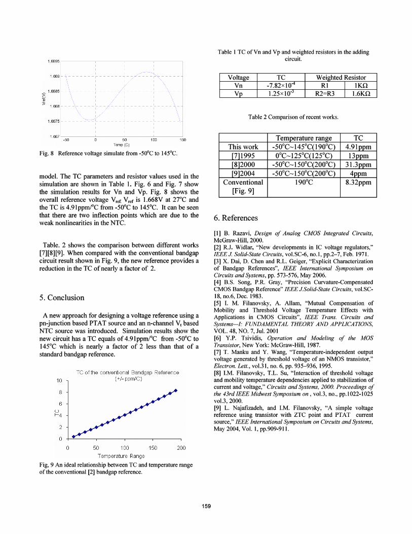
Fig, 9 An ideal relationship between TC and temperature rangeof the conventional [2] bandgap reference.
159