Embed Size (px)
Citation preview
GVDD
GVDD
PVDD
M
Controller
RESET_A
PWM_B
OC_ADJ
GND
GND_A
GND_B
OUT_B
PVDD_B
AGND
VREG
M3
M2
BST_B
NC
NC
GND
RESET_C
RESET_B
VDD
GVDD_C
OUT_C
PVDD_C
BST_C
GVDD_C
PWM_C GND_C
M1 GND
GVDD_B
OTW
FAULT
PWM_A
GVDD_A
BST_A
PVDD_A
OUT_A
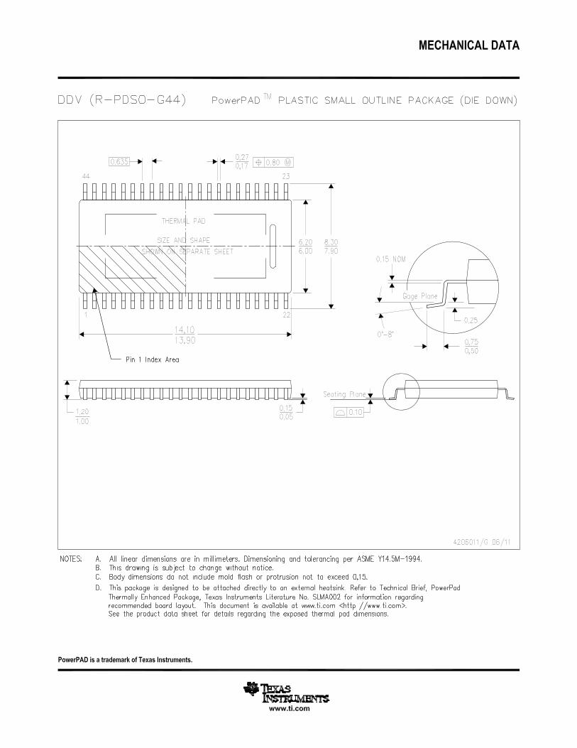
DRV8332-HT
www.ti.com SLES274B –AUGUST 2013–REVISED JANUARY 2014
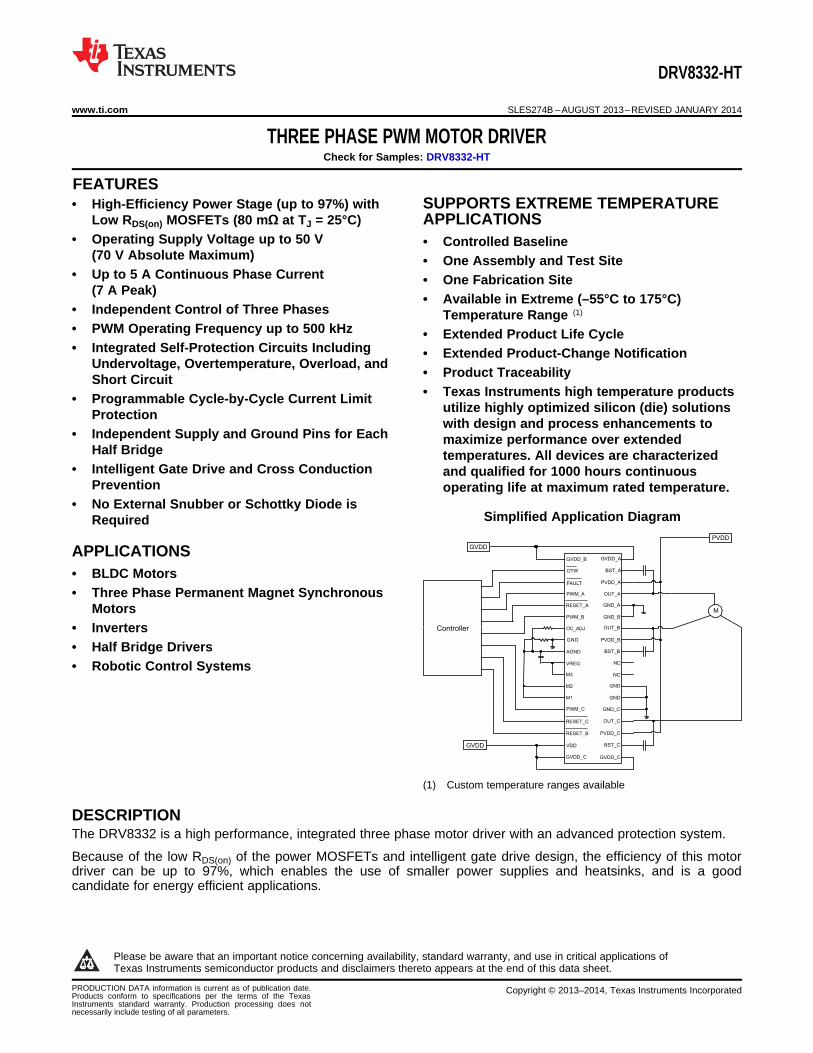
THREE PHASE PWM MOTOR DRIVERCheck for Samples: DRV8332-HT
1FEATURES• High-Efficiency Power Stage (up to 97%) with SUPPORTS EXTREME TEMPERATURE
Low RDS(on) MOSFETs (80 mΩ at TJ = 25°C) APPLICATIONS• Operating Supply Voltage up to 50 V • Controlled Baseline
(70 V Absolute Maximum) • One Assembly and Test Site• Up to 5 A Continuous Phase Current • One Fabrication Site
(7 A Peak) • Available in Extreme (–55°C to 175°C)• Independent Control of Three Phases Temperature Range (1)
• PWM Operating Frequency up to 500 kHz • Extended Product Life Cycle• Integrated Self-Protection Circuits Including • Extended Product-Change Notification
Undervoltage, Overtemperature, Overload, and • Product TraceabilityShort Circuit• Texas Instruments high temperature products• Programmable Cycle-by-Cycle Current Limit utilize highly optimized silicon (die) solutionsProtection with design and process enhancements to
• Independent Supply and Ground Pins for Each maximize performance over extendedHalf Bridge temperatures. All devices are characterized
• Intelligent Gate Drive and Cross Conduction and qualified for 1000 hours continuousPrevention operating life at maximum rated temperature.
• No External Snubber or Schottky Diode isSimplified Application DiagramRequired
APPLICATIONS• BLDC Motors• Three Phase Permanent Magnet Synchronous
Motors• Inverters• Half Bridge Drivers• Robotic Control Systems
(1) Custom temperature ranges available
DESCRIPTIONThe DRV8332 is a high performance, integrated three phase motor driver with an advanced protection system.
Because of the low RDS(on) of the power MOSFETs and intelligent gate drive design, the efficiency of this motordriver can be up to 97%, which enables the use of smaller power supplies and heatsinks, and is a goodcandidate for energy efficient applications.
1
Please be aware that an important notice concerning availability, standard warranty, and use in critical applications ofTexas Instruments semiconductor products and disclaimers thereto appears at the end of this data sheet.
PRODUCTION DATA information is current as of publication date. Copyright © 2013–2014, Texas Instruments IncorporatedProducts conform to specifications per the terms of the TexasInstruments standard warranty. Production processing does notnecessarily include testing of all parameters.
DRV8332-HT
SLES274B –AUGUST 2013–REVISED JANUARY 2014 www.ti.com
DESCRIPTION (CONTINUED)The DRV8332 requires two power supplies, one at 12 V for GVDD and VDD, and another up to 50 V for PVDD.The DRV8332 can operate at up to 500-kHz switching frequency while still maintain precise control and highefficiency. It also has an innovative protection system safeguarding the device against a wide range of faultconditions that could damage the system. These safeguards are short-circuit protection, overcurrent protectionand undervoltage protection. The DRV8332 has a current-limiting circuit that prevents device shutdown duringload transients such as motor start-up. A programmable overcurrent detector allows adjustable current limit andprotection level to meet different motor requirements.
The DRV8332 has unique independent supply and ground pins for each half bridge, which makes it possible toprovide current measurement through external shunt resistor and support half bridge drivers with different powersupply voltage requirements.
2 Submit Documentation Feedback Copyright © 2013–2014, Texas Instruments Incorporated
Product Folder Links: DRV8332-HT
DRV8332-HT
www.ti.com SLES274B –AUGUST 2013–REVISED JANUARY 2014
This integrated circuit can be damaged by ESD. Texas Instruments recommends that all integrated circuits be handled withappropriate precautions. Failure to observe proper handling and installation procedures can cause damage.
ESD damage can range from subtle performance degradation to complete device failure. Precision integrated circuits may be moresusceptible to damage because very small parametric changes could cause the device not to meet its published specifications.
ORDERING INFORMATION (1)
TA PACKAGE ORDERABLE PART NUMBER TOP-SIDE MARKING–55°C to 175°C DDV DRV8332HDDV DRV8332H
(1) For the most current package and ordering information, see the Package Option Addendum at the end of this document, or see the TIwebsite at www.ti.com.
ABSOLUTE MAXIMUM RATINGSOver operating free-air temperature range unless otherwise noted (1)
VALUEVDD to GND –0.3 V to 13.2 VGVDD_X to GND –0.3 V to 13.2 VPVDD_X to GND_X (2) –0.3 V to 70 VOUT_X to GND_X (2) –0.3 V to 70 VBST_X to GND_X (2) –0.3 V to 80 VMaximum bootstrap in rush current, IBST_In 0.4 ATransient peak output current (per pin), pulse width limited by internal over-current protection circuit. 16 ATransient peak output current for latch shut down (per pin) 20 AVREG to AGND –0.3 V to 4.2 VGND_X to GND –0.3 V to 0.3 VGND to AGND –0.3 V to 0.3 VPWM_X, RESET_X to GND –0.3 V to 4.2 VOC_ADJ, M1, M2, M3 to AGND –0.3 V to 4.2 VFAULT, OTW to GND –0.3 V to 7 VMaximum continuous sink current (FAULT, OTW) 9 mAMaximum operating junction temperature range, TJ -55°C to 185°CStorage temperature, TSTG –55°C to 175°C
(1) Stresses beyond those listed under Absolute Maximum Ratings may cause permanent damage to the device. These are stress ratingsonly, and functional operation of the device at these or any other conditions beyond those indicated under Recommended OperatingConditions is not implied. Exposure to absolute-maximum-rated conditions for extended periods may affect device reliability.
(2) These voltages represent the dc voltage + peak ac waveform measured at the terminal of the device in all conditions.
RECOMMENDED OPERATING CONDITIONSMIN NOM MAX UNIT
PVDD_X Half bridge X (A, B, or C) DC supply voltage 0 50 52.5 VGVDD_X Supply for logic regulators and gate-drive circuitry 10.8 12 13.2 VVDD Digital regulator supply voltage 10.8 12 13.2 VIO_PULSE Pulsed peak current per output pin (could be limited by thermal) 7 AIO Continuous current per output pin (DRV8332) 5 AFSW PWM switching frequency 380 kHzROCP_CBC OC programming resistor range in cycle-by-cycle current limit modes 30 200 kΩCBST Bootstrap capacitor range 33 220 nFTON_MIN Minimum PWM pulse duration, low side 50 nsTJ Operating junction temperature -55 175 °C
Copyright © 2013–2014, Texas Instruments Incorporated Submit Documentation Feedback 3
Product Folder Links: DRV8332-HT
DRV8332-HT
SLES274B –AUGUST 2013–REVISED JANUARY 2014 www.ti.com
THERMAL INFORMATIONDRV8332-HT
THERMAL METRIC (1) DDV UNITS44 PINS
θJA Junction-to-ambient thermal resistance (2) 42.6θJCtop Junction-to-case (top) thermal resistance (3) 0.2θJB Junction-to-board thermal resistance (4) 17.4
°C/WψJT Junction-to-top characterization parameter (5) 0.5ψJB Junction-to-board characterization parameter (6) 17.4θJCbot Junction-to-case (bottom) thermal resistance (7) N/A
(1) For more information about traditional and new thermal metrics, see the IC Package Thermal Metrics application report, SPRA953.(2) The junction-to-ambient thermal resistance under natural convection is obtained in a simulation on a JEDEC-standard, high-K board, as
specified in JESD51-7, in an environment described in JESD51-2a.(3) The junction-to-case (top) thermal resistance is obtained by simulating a cold plate test on the package top. No specific JEDEC-
standard test exists, but a close description can be found in the ANSI SEMI standard G30-88.(4) The junction-to-board thermal resistance is obtained by simulating in an environment with a ring cold plate fixture to control the PCB
temperature, as described in JESD51-8.(5) The junction-to-top characterization parameter, ψJT, estimates the junction temperature of a device in a real system and is extracted
from the simulation data for obtaining θJA, using a procedure described in JESD51-2a (sections 6 and 7).(6) The junction-to-board characterization parameter, ψJB, estimates the junction temperature of a device in a real system and is extracted
from the simulation data for obtaining θJA , using a procedure described in JESD51-2a (sections 6 and 7).(7) The junction-to-case (bottom) thermal resistance is obtained by simulating a cold plate test on the exposed (power) pad. No specific
JEDEC standard test exists, but a close description can be found in the ANSI SEMI standard G30-88.Spacer
MODE SELECTION PINS
MODE PINS OUTPUT DESCRIPTIONCONFIGURATIONM3 M2 M11 0 0 1 3PH or 3 HB Three-phase or three half bridges with cycle-by-cycle current limit
Three-phase or three half bridges with OC latching shutdown (no cycle-by-1 0 1 1 3PH or 3 HB cycle current limit)0 x x Reserved1 1 x Reserved
4 Submit Documentation Feedback Copyright © 2013–2014, Texas Instruments Incorporated
Product Folder Links: DRV8332-HT
1
2
3
4
5
6
7
8
9
10
11
12
13
14
15
16
17
18
19
20
21
22
GVDD_B
VDD
NC
NC
PWM_C
RESET_A
OC_ADJ
GND
VREG
AGND
M1
M2
M3
PWM_A
RESET_B
PWM_B
NC
FAULT
NC
OTW
GVDD_C
GVDD_A
BST_A
NC
PVDD_A
PVDD_A
OUT_A
GND_A
GND_B
OUT_B
NC
NC
BST_B
PVDD_B
GND
GND
GND_C
OUT_C
PVDD_C
PVDD_C
NC
BST_C
GVDD_C
44
43
42
41
40
39
38
37
36
35
34
33
32
31
30
29
28
27
26
25
24
23
RESET_C
DRV8332-HT
www.ti.com SLES274B –AUGUST 2013–REVISED JANUARY 2014
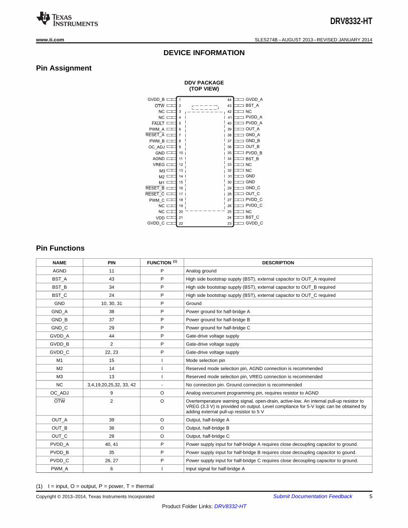
DEVICE INFORMATION
Pin Assignment
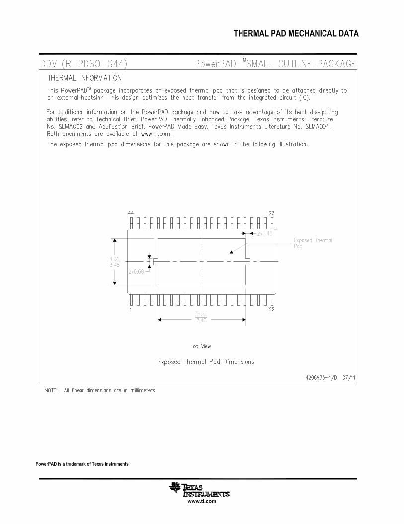
DDV PACKAGE(TOP VIEW)
Pin Functions
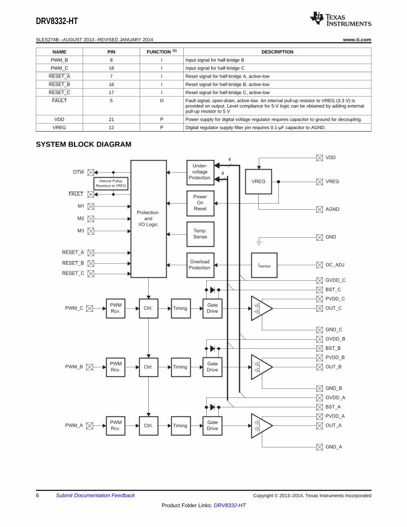
NAME PIN FUNCTION (1) DESCRIPTION
AGND 11 P Analog ground
BST_A 43 P High side bootstrap supply (BST), external capacitor to OUT_A required
BST_B 34 P High side bootstrap supply (BST), external capacitor to OUT_B required
BST_C 24 P High side bootstrap supply (BST), external capacitor to OUT_C required
GND 10, 30, 31 P Ground
GND_A 38 P Power ground for half-bridge A
GND_B 37 P Power ground for half-bridge B
GND_C 29 P Power ground for half-bridge C
GVDD_A 44 P Gate-drive voltage supply
GVDD_B 2 P Gate-drive voltage supply
GVDD_C 22, 23 P Gate-drive voltage supply
M1 15 I Mode selection pin
M2 14 I Reserved mode selection pin, AGND connection is recommended
M3 13 I Reserved mode selection pin, VREG connection is recommended
NC 3,4,19,20,25,32, 33, 42 - No connection pin. Ground connection is recommended
OC_ADJ 9 O Analog overcurrent programming pin, requires resistor to AGND
OTW 2 O Overtemperature warning signal, open-drain, active-low. An internal pull-up resistor toVREG (3.3 V) is provided on output. Level compliance for 5-V logic can be obtained byadding external pull-up resistor to 5 V
OUT_A 39 O Output, half-bridge A
OUT_B 36 O Output, half-bridge B
OUT_C 28 O Output, half-bridge C
PVDD_A 40, 41 P Power supply input for half-bridge A requires close decoupling capacitor to ground.
PVDD_B 35 P Power supply input for half-bridge B requires close decoupling capacitor to gound.
PVDD_C 26, 27 P Power supply input for half-bridge C requires close decoupling capacitor to ground.
PWM_A 6 I Input signal for half-bridge A
(1) I = input, O = output, P = power, T = thermal
Copyright © 2013–2014, Texas Instruments Incorporated Submit Documentation Feedback 5
Product Folder Links: DRV8332-HT
Temp.
Sense
M1
M2
RESET_A
FAULT
OTW
AGND
OC_ADJ
VREG VREG
VDD
M3
Power
On
Reset
Under-
voltage
Protection
GND
PWM_C OUT_C
GND_C
PVDD_C
BST_C
TimingGate
Drive
PWM
Rcv.
Overload
ProtectionIsense
GVDD_C
RESET_B
4
Protection
and
I/O Logic
PWM_B OUT_B
GND_B
PVDD_B
BST_B
TimingGate
DriveCtrl.
PWM
Rcv.
GVDD_B
PWM_A OUT_A
GND_A
PVDD_A
BST_A
TimingGate
DriveCtrl.
PWM
Rcv.
GVDD_A
Ctrl.
Internal Pullup
Resistors to VREG
4
RESET_C
DRV8332-HT
SLES274B –AUGUST 2013–REVISED JANUARY 2014 www.ti.com
NAME PIN FUNCTION (1) DESCRIPTION
PWM_B 8 I Input signal for half-bridge B
PWM_C 18 I Input signal for half-bridge C
RESET_A 7 I Reset signal for half-bridge A, active-low
RESET_B 16 I Reset signal for half-bridge B, active-low
RESET_C 17 I Reset signal for half-bridge C, active-low
FAULT 5 O Fault signal, open-drain, active-low. An internal pull-up resistor to VREG (3.3 V) isprovided on output. Level compliance for 5-V logic can be obtained by adding externalpull-up resistor to 5 V
VDD 21 P Power supply for digital voltage regulator requires capacitor to ground for decoupling.
VREG 12 P Digital regulator supply filter pin requires 0.1-μF capacitor to AGND.
SYSTEM BLOCK DIAGRAM
6 Submit Documentation Feedback Copyright © 2013–2014, Texas Instruments Incorporated
Product Folder Links: DRV8332-HT
DRV8332-HT
www.ti.com SLES274B –AUGUST 2013–REVISED JANUARY 2014
ELECTRICAL CHARACTERISTICSTJ = -55°C to 175°C, PVDD = 50 V, GVDD = VDD = 12 V, fSw = 380 kHz, unless otherwise noted. All performance is inaccordance with recommended operating conditions unless otherwise specified.
PARAMETER TEST CONDITIONS MIN TYP MAX UNIT
Internal Voltage Regulator and Current Consumption
VREG Voltage regulator, only used as a reference node VDD = 12 V 2.85 3.3 3.75 V
Idle, reset mode 9 15 mAIVDD VDD supply current
Operating, 50% duty cycle 10.5
Reset mode 1.7 2.5 mAIGVDD_X Gate supply current per half-bridge
Operating, 50% duty cycle 8
IPVDD_X Half-bridge X (A, B, or C) idle current Reset mode 0.7 1 mA
Output Stage
MOSFET drain-to-source resistance, low side (LS) TJ = 25°C, GVDD = 12 V 260 mΩRDS(on)
MOSFET drain-to-source resistance, high side (HS) TJ = 25°C, GVDD = 12 V 260 mΩ
VF Diode forward voltage drop TJ = 25°C - 125°C, IO = 5 A 1 V
tR Output rise time Resistive load, IO = 5 A 14 ns
tF Output fall time Resistive load, IO = 5 A 14 ns
tPD_ON Propagation delay when FET is on Resistive load, IO = 5 A 38 ns
tPD_OFF Propagation delay when FET is off Resistive load, IO = 5 A 38 ns
tDT Dead time between HS and LS FETs Resistive load, IO = 5 A 5.5 ns
I/O Protection
Gate supply voltage GVDD_X undervoltageVuvp,G 8.5 Vprotection threshold
Vuvp,hyst(1) Hysteresis for gate supply undervoltage event 0.3 V
IOC Overcurrent limit protection Resistor—programmable, nominal, ROCP = 36 kΩ 7.4 A
Time from application of short condition to Hi-Z ofIOCT Overcurrent response time 250 nsaffected FET(s)
Static Digital Specifications
VIH High-level input voltage PWM_A, PWM_B, PWM_C, M1, M2, M3 2 3.6 V
VIH High-level input voltage RESET_A, RESET_B, RESET_C 2 3.6 V
PWM_A, PWM_B, PWM_C, M1, M2, M3,VIL Low-level input voltage 0.8 VRESET_A, RESET_B, RESET_C
llkg Input leakage current -100 100 μA
OTW / FAULT
Internal pullup resistance, OTW to VREG, FAULT toRINT_PU 20 26 35 kΩVREG
VOH High-level output voltage Internal pullup resistor only 1.95 3.3 3.65 V
VOL Low-level output voltage IO = 4 mA 0.2 0.4 V
(1) Specified by design
Copyright © 2013–2014, Texas Instruments Incorporated Submit Documentation Feedback 7
Product Folder Links: DRV8332-HT
1000.00
10000.00
100000.00
120 130 140 150 160 170 180 190
Esti
mate
d L
ife (
Ho
urs
)
Operating Junction Temperature (°C)
DRV8332-HT
SLES274B –AUGUST 2013–REVISED JANUARY 2014 www.ti.com
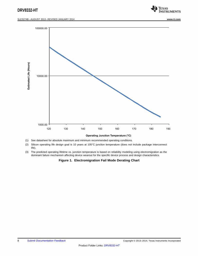
(1) See datasheet for absolute maximum and minimum recommended operating conditions.(2) Silicon operating life design goal is 10 years at 105°C junction temperature (does not include package interconnect
life).(3) The predicted operating lifetime vs. junction temperature is based on reliability modeling using electromigration as the
dominant failure mechanism affecting device wearout for the specific device process and design characteristics.
Figure 1. Electromigration Fail Mode Derating Chart
8 Submit Documentation Feedback Copyright © 2013–2014, Texas Instruments Incorporated
Product Folder Links: DRV8332-HT
0.985
0.990
0.995
1.000
1.005
1.010
1.015
1.020
±55 ±30 ±5 20 45 70 95 120 145 170
No
rmal
ized
RD
S(o
n) /
RD
S(o
n) a
t 25C
)
TJ ± Junction Temperature ± C C001
GVDD = 12 V
–1
5
0
1
2
3
V – Voltage – V
I–
Cu
rren
t–
A
1.20.80 10.60.2 0.4
4
6
T = 25°CJ
0
100
40
50
60
70
80
90
Eff
icie
ncy
–%
f – Switching Frequency – kHz
0 100 150 200 250 300 350 400 450 50050
10
20
30
Load = 5 APVDD = 50 VT = 75°C
Full Bridge
C
1.10
0.96
1.00
0.98
1.02
1.04
GVDD – Gate Drive – V
No
rmalized
R/ (R
at
12 V
)D
S(o
n)
DS
(on
)11.010.08.0 10.59.58.5 9.0 11.5
1.06
1.08
12
T = 25°CJ
DRV8332-HT
www.ti.com SLES274B –AUGUST 2013–REVISED JANUARY 2014
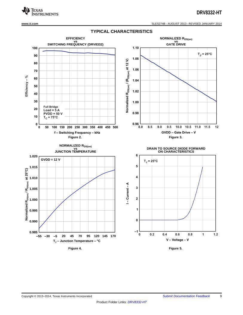
TYPICAL CHARACTERISTICSEFFICIENCY NORMALIZED RDS(on)
vs vsSWITCHING FREQUENCY (DRV8332) GATE DRIVE
Figure 2. Figure 3.
NORMALIZED RDS(on)vs DRAIN TO SOURCE DIODE FORWARD
JUNCTION TEMPERATURE ON CHARACTERISTICS
Figure 4. Figure 5.
Copyright © 2013–2014, Texas Instruments Incorporated Submit Documentation Feedback 9
Product Folder Links: DRV8332-HT
0
100
10
20
30
40
50
60
70
80
90
Ou
tpu
t D
uty
Cycle
–%
Input Duty Cycle – %
9060 1000 70402010 30 50 80
f = 500 kHz
T = 25°CS
C
DRV8332-HT
SLES274B –AUGUST 2013–REVISED JANUARY 2014 www.ti.com
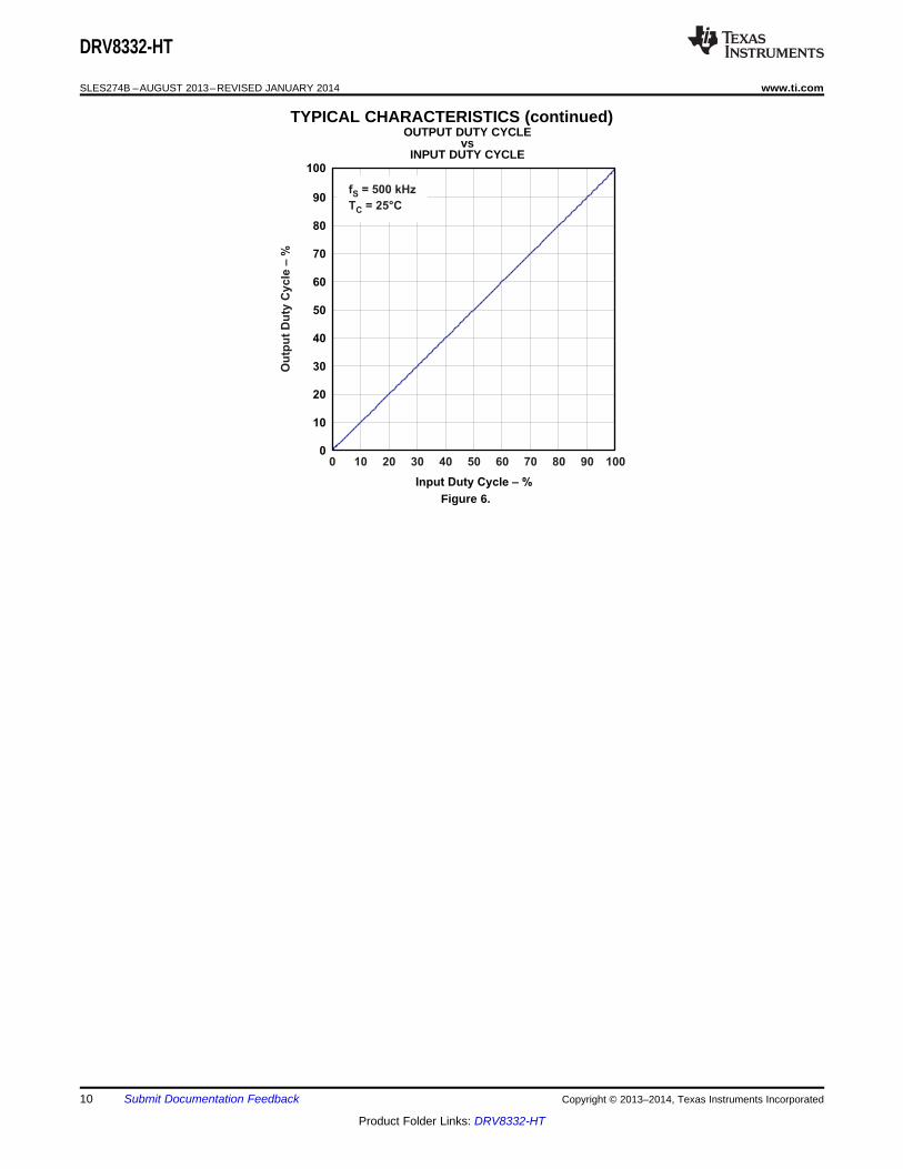
TYPICAL CHARACTERISTICS (continued)OUTPUT DUTY CYCLE
vsINPUT DUTY CYCLE
Figure 6.
10 Submit Documentation Feedback Copyright © 2013–2014, Texas Instruments Incorporated
Product Folder Links: DRV8332-HT
DRV8332-HT
www.ti.com SLES274B –AUGUST 2013–REVISED JANUARY 2014
THEORY OF OPERATION
Special attention should be paid to the power-stagePOWER SUPPLIES power supply; this includes component selection, androuting. As indicated, each half-bridge hasTo facilitate system design, the DRV8332 needs onlyindependent power-stage supply pin (PVDD_X). Fora 12-V supply in addition to H-Bridge power supplyoptimal electrical performance, EMI compliance, and(PVDD). An internal voltage regulator providessystem reliability, it is important that each PVDD_Xsuitable voltage levels for the digital and low-voltagepin is decoupled with a ceramic capacitor (X5R oranalog circuitry. Additionally, the high-side gate drivebetter) placed as close as possible to each supplyrequiring a floating voltage supply, which ispin.accommodated by built-in bootstrap circuitry requiring
external bootstrap capacitor. The 12-V supply should be from a low-noise, low-output-impedance voltage regulator. Likewise, the 50-To provide symmetrical electrical characteristics, theV power-stage supply is assumed to have low outputPWM signal path, including gate drive and outputimpedance and low noise. The power-supplystage, is designed as identical, independent half-sequence is not critical as facilitated by the internalbridges. For this reason, each half-bridge has apower-on-reset circuit. Moreover, the DRV8332 areseparate gate drive supply (GVDD_X), a bootstrapfully protected against erroneous power-stage turn-onpin (BST_X), and a power-stage supply pindue to parasitic gate charging. Thus, voltage-supply(PVDD_X). Furthermore, an additional pin (VDD) isramp rates (dv/dt) are non-critical within the specifiedprovided as supply for all common circuits. Specialvoltage range (see the Recommended Operatingattention should be paid to place all decouplingConditions section of this data sheet).capacitors as close to their associated pins as
possible. In general, inductance between the powersupply pins and decoupling capacitors must be SYSTEM POWER-UP/POWER-DOWNavoided. Furthermore, decoupling capacitors need a SEQUENCEshort ground path back to the device.
Powering UpFor a properly functioning bootstrap circuit, a smallceramic capacitor (an X5R or better) must be The DRV8332 does not require a power-upconnected from each bootstrap pin (BST_X) to the sequence. The outputs of the H-bridges remain in apower-stage output pin (OUT_X). When the power- high impedance state until the gate-drive supplystage output is low, the bootstrap capacitor is voltage GVDD_X and VDD voltage are above thecharged through an internal diode connected undervoltage protection (UVP) voltage threshold (seebetween the gate-drive power-supply pin (GVDD_X) the Electrical Characteristics section of this dataand the bootstrap pin. When the power-stage output sheet). Although not specifically required, holdingis high, the bootstrap capacitor potential is shifted RESET_A, RESET_B, and RESET_C in a low stateabove the output potential and thus provides a while powering up the device is recommended. Thissuitable voltage supply for the high-side gate driver. allows an internal circuit to charge the externalIn an application with PWM switching frequencies in bootstrap capacitors by enabling a weak pulldown ofthe range from 10 kHz to 500 kHz, the use of 100-nF the half-bridge output.ceramic capacitors (X5R or better), size 0603 or0805, is recommended for the bootstrap supply. Powering DownThese 100-nF capacitors ensure sufficient energy The DRV8332 does not require a power-downstorage, even during minimal PWM duty cycles, to sequence. The device remains fully operational askeep the high-side power stage FET fully turned on long as the gate-drive supply (GVDD_X) voltage andduring the remaining part of the PWM cycle. In an VDD voltage are above the UVP voltage thresholdapplication running at a switching frequency lower (see the Electrical Characteristics section of this datathan 10 kHz, the bootstrap capacitor might need to be sheet). Although not specifically required, it is a goodincreased in value. practice to hold RESET_A, RESET_B and RESET_C
low during power down to prevent any unknown stateduring this transition.
Copyright © 2013–2014, Texas Instruments Incorporated Submit Documentation Feedback 11
Product Folder Links: DRV8332-HT
DRV8332-HT
SLES274B –AUGUST 2013–REVISED JANUARY 2014 www.ti.com
Bootstrap Capacitor Under Voltage ProtectionERROR REPORTINGWhen the device runs at a low switching frequencyThe FAULT and OTW pins are both active-low, open-(e.g. less than 10 kHz with a 100-nF bootstrapdrain outputs. Their function is for protection-modecapacitor), the bootstrap capacitor voltage might notsignaling to a PWM controller or other system-controlbe able to maintain a proper voltage level for thedevice.high-side gate driver. A bootstrap capacitor
Any fault resulting in device shutdown, such as undervoltage protection circuit (BST_UVP) willovertemperatue shut down, overcurrent shut-down, or prevent potential failure of the high-side MOSFET.undervoltage protection, is signaled by the FAULT pin When the voltage on the bootstrap capacitors is lessgoing low. Likewise, OTW goes low when the device than the required value for safe operation, thejunction temperature exceeds 125°C (see Table 1). DRV8332 will initiate bootstrap capacitor recharge
sequences (turn off high side FET for a short period)Table 1. Protection Mode Signal Descriptions until the bootstrap capacitors are properly charged for
safe operation. This function may also be activatedFAULT OTW DESCRIPTIONwhen PWM duty cycle is too high (e.g. less than 200 0 Overtemperature warning andns off time at 10 kHz). Note that bootstrap capacitor(overtemperature shut down or overcurrent
shut down or undervoltage protection) occurred might not be able to be charged if no load orextremely light load is presented at output during0 1 Overcurrent shut-down or GVDD undervoltage
protection occurred BST_UVP operation, so it is recommended to turn onthe low side FET for at least 50 ns for each PWM1 0 Overtemperature warningcycle to avoid BST_UVP operation if possible.1 1 Device under normal operation
For all applications, it is recommended to add 26-ΩTI recommends monitoring the OTW signal using the resistor between the GVDD power supply andsystem microcontroller and responding to an OTW GVDD_X pins to limit the inrush current on thesignal by reducing the load current to prevent further internal bootstrap diodes.heating of the device resulting in deviceovertemperature shutdown (OTSD).
Overcurrent (OC) ProtectionTo reduce external component count, an internal
The DRV8332 has independent, fast-reacting currentpullup resistor to internal VREG (3.3 V) is provided ondetectors with programmable trip threshold (OCboth FAULT and OTW outputs. Level compliance forthreshold) on all high-side and low-side power-stage5-V logic can be obtained by adding external pull-upFETs. There are two settings for OC protectionresistors to 5 V (see the Electrical Characteristicsthrough mode selection pins: cycle-by-cycle (CBC)section of this data sheet for further specifications).current limiting mode and OC latching (OCL) shutdown mode.DEVICE PROTECTION SYSTEMIn CBC current limiting mode, the detector outputsThe DRV8332 contains advanced protection circuitry are monitored by two protection systems. The firstcarefully designed to facilitate system integration and protection system controls the power stage in order toease of use, as well as to safeguard the device from prevent the output current from further increasing,permanent failure due to a wide range of fault i.e., it performs a CBC current-limiting function ratherconditions such as short circuits, overcurrent, than prematurely shutting down the device. Thisovertemperature, and undervoltage. The DRV8332 feature could effectively limit the inrush current duringresponds to a fault by immediately setting the half motor start-up or transient without damaging thebridge outputs in a high-impedance (Hi-Z) state and device. During short to power and short to groundasserting the FAULT pin low. In situations other than conditions, the current limit circuitry might not be ableovercurrent or overtemperature, the device to control the current to a proper level, a secondautomatically recovers when the fault condition has protection system triggers a latching shutdown,been removed or the gate supply voltage has resulting in the related half bridge being set in theincreased. For highest possible reliability, reset the high-impedance (Hi-Z) state. Current limiting anddevice externally no sooner than 1 second after the overcurrent protection are independent for half-shutdown when recovering from an overcurrent shut bridges A, B, and C, respectively.down (OCSD) or OTSD fault.
12 Submit Documentation Feedback Copyright © 2013–2014, Texas Instruments Incorporated
Product Folder Links: DRV8332-HT
DRV8332-HT
www.ti.com SLES274B –AUGUST 2013–REVISED JANUARY 2014
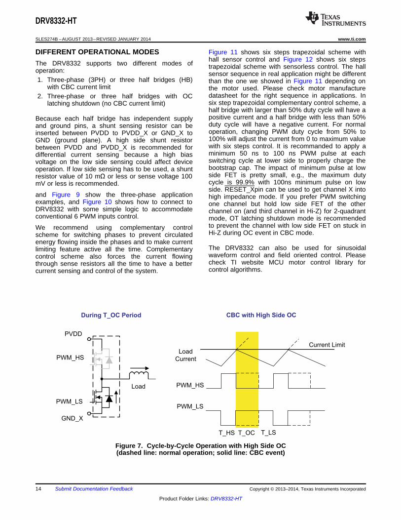
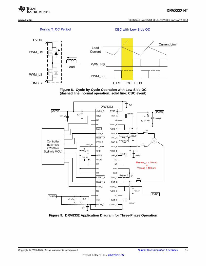
Figure 7 illustrates cycle-by-cycle operation with high Table 2. Programming-Resistor Values and OCside OC event and Figure 8 shows cycle-by-cycle Threshold (continued)operation with low side OC. Dashed lines are the OC-ADJUST RESISTOR MAXIMUM CURRENT BEFOREoperation waveforms when no CBC event is triggered VALUES (kΩ) OC OCCURS (A)and solide lines show the waveforms when CBC 82 3.4event is triggered. In CBC current limiting mode,
100 2.8when low side FET OC is detected, the device will120 2.4turn off the affected low side FET and keep the high
side FET at the same half bridge off until next PWM 150 1.9cycle; when high side FET OC is detected, the device 200 1.4will turn off the affected high side FET and turn on thelow side FET at the half bridge until next PWM cycle. It should be noted that a properly functioning
overcurrent detector assumes the presence of aIt is important to note that if the input to a half bridge proper inductor or power ferrite bead at the power-is held to a constant value when an over current stage output. Short-circuit protection is notevent occurs in CBC, then the associated half bridge guaranteed with direct short at the output pins of thewill be in a HI-Z state upon the over current event power stage.ending. Cycling IN_X will allow OUT_X to resumenormal operation. Undervoltage Protection (UVP) and Power-On
Reset (POR)In OC latching shut down mode, the CBC current limitand error recovery circuits are disabled and an The UVP and POR circuits of the DRV8332 fullyovercurrent condition will cause the device to protect the device in any power-up / down andshutdown immediately. After shutdown, RESET_A, brownout situation. While powering up, the PORRESET_B, and RESET_C must be asserted to circuit resets the overcurrent circuit and ensures thatrestore normal operation after the overcurrent all circuits are fully operational when the GVDD_Xcondition is removed. and VDD supply voltages reach 9.8 V (typical).
Although GVDD_X and VDD are independentlyFor added flexibility, the OC threshold ismonitored, a supply voltage drop below the UVPprogrammable using a single external resistorthreshold on any VDD or GVDD_X pin results in allconnected between the OC_ADJ pin and AGND pin.half-bridge outputs immediately being set in the high-See Table 2 for information on the correlationimpedance (Hi-Z) state and FAULT being assertedbetween programming-resistor value and the OClow. The device automatically resumes operationthreshold.when all supply voltage on the bootstrap capacitors
The values in Table 2 show typical OC thresholds for have increased above the UVP threshold.a given resistor. Assuming a fixed resistance on theOC_ADJ pin across multiple devices, a 20% device- DEVICE RESETto-device variation in OC threshold measurements ispossible. Therefore, this system is designed for Three reset pins are provided for independent controlsystem protection and not for precise current control. of half-bridges A, B, and C. When RESET_X is
asserted low, two power-stage FETs in half-bridges XTable 2. Programming-Resistor Values and OC are forced into a high-impedance (Hi-Z) state.
ThresholdA rising-edge transition on reset input allows the
OC-ADJUST RESISTOR MAXIMUM CURRENT BEFORE device to resume operation after a shut-down fault.VALUES (kΩ) OC OCCURS (A) That is, when half-bridge X has OC shutdown in CBC
30 8.8 mode, a low to high transition of RESET_X pin will36 7.4 clear the fault and FAULT pin. When an OTSD
occurs or OC shutdown in Latching mode occurs, all39 6.9three RESET_A, RESET_B, and RESET_C need to43 6.3have a low to high transition to clear the fault and
47 5.8 reset FAULT signal.56 4.968 4.1
Copyright © 2013–2014, Texas Instruments Incorporated Submit Documentation Feedback 13
Product Folder Links: DRV8332-HT
PWM_HS
PWM_LS
Load
Current
Current Limit
T_HS T_OC
PVDD
GND_X
PWM_HS
PWM_LS
Load
T_LS
CBC with High Side OCDuring T_OC Period
DRV8332-HT
SLES274B –AUGUST 2013–REVISED JANUARY 2014 www.ti.com
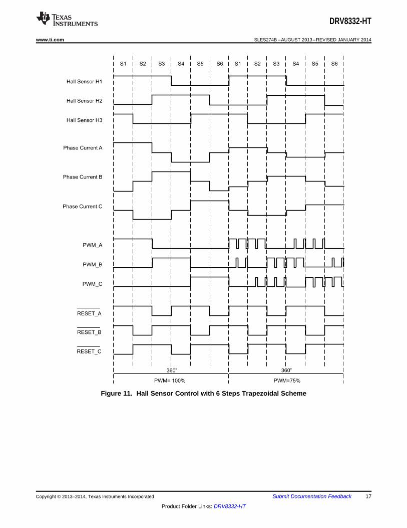
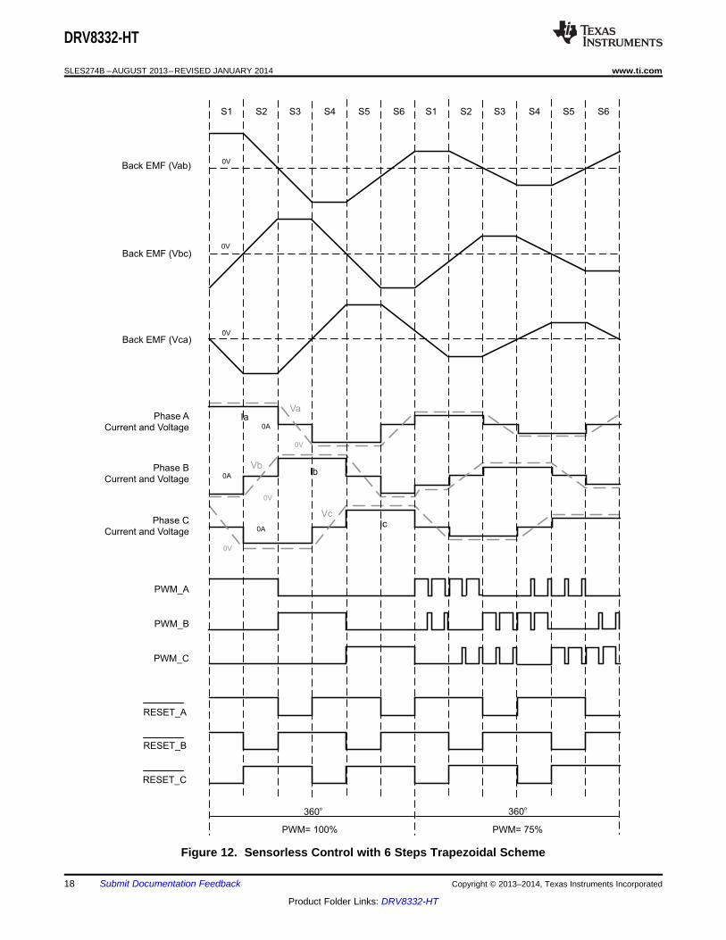
DIFFERENT OPERATIONAL MODES Figure 11 shows six steps trapezoidal scheme withhall sensor control and Figure 12 shows six stepsThe DRV8332 supports two different modes of trapezoidal scheme with sensorless control. The halloperation: sensor sequence in real application might be different
1. Three-phase (3PH) or three half bridges (HB) than the one we showed in Figure 11 depending onwith CBC current limit the motor used. Please check motor manufacture
datasheet for the right sequence in applications. In2. Three-phase or three half bridges with OCsix step trapezoidal complementary control scheme, alatching shutdown (no CBC current limit)half bridge with larger than 50% duty cycle will have apositive current and a half bridge with less than 50%Because each half bridge has independent supplyduty cycle will have a negative current. For normaland ground pins, a shunt sensing resistor can beoperation, changing PWM duty cycle from 50% toinserted between PVDD to PVDD_X or GND_X to100% will adjust the current from 0 to maximum valueGND (ground plane). A high side shunt resistorwith six steps control. It is recommanded to apply abetween PVDD and PVDD_X is recommended forminimum 50 ns to 100 ns PWM pulse at eachdifferential current sensing because a high biasswitching cycle at lower side to properly charge thevoltage on the low side sensing could affect devicebootstrap cap. The impact of minimum pulse at lowoperation. If low side sensing has to be used, a shuntside FET is pretty small, e.g., the maximum dutyresistor value of 10 mΩ or less or sense voltage 100cycle is 99.9% with 100ns minimum pulse on lowmV or less is recommended.side. RESET_Xpin can be used to get channel X into
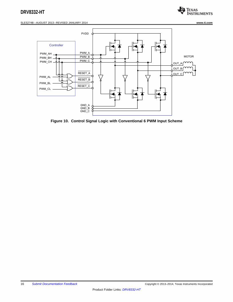
and Figure 9 show the three-phase application high impedance mode. If you prefer PWM switchingexamples, and Figure 10 shows how to connect to one channel but hold low side FET of the otherDRV8332 with some simple logic to accommodate channel on (and third channel in Hi-Z) for 2-quadrantconventional 6 PWM inputs control. mode, OT latching shutdown mode is recommended
to prevent the channel with low side FET on stuck inWe recommend using complementary controlHi-Z during OC event in CBC mode.scheme for switching phases to prevent circulated
energy flowing inside the phases and to make currentThe DRV8332 can also be used for sinusoidallimiting feature active all the time. Complementarywaveform control and field oriented control. Pleasecontrol scheme also forces the current flowingcheck TI website MCU motor control library forthrough sense resistors all the time to have a bettercontrol algorithms.current sensing and control of the system.
Figure 7. Cycle-by-Cycle Operation with High Side OC(dashed line: normal operation; solid line: CBC event)
14 Submit Documentation Feedback Copyright © 2013–2014, Texas Instruments Incorporated
Product Folder Links: DRV8332-HT
OTW BST_A
GVDD
GVDD
PVDD
PVDD
1000 Fm
Loc
Loc
Loc
3.3
10 nF
100 nF
100 nF
100 nF
1 Fm
1 Fm
1 Fm
47 Fm
330 Fm
Controller
(MSP430
C2000 or
Stellaris MCU)
RESET_A
PWM_B
OC_ADJ
GND
GND_A
GND_B
OUT_B
PVDD_B
AGND
VREG
M3
M2
BST_B
NC
NC
GND
RESET_C
PWM_C
NC
NC
OUT_C
PVDD_C
PVDD_C
NC
RESET_B GND_C
M1 GND
NC
NC
FAULT
PWM_A
NC
PVDD_A
PVDD_A
OUT_A
100nF
100nF
100nF
MRsense_B
Rsense_C
Rsense_A
Rsense_x
or
Vsense < 100 mV
£ 10 mW
GVDD_B GVDD_A
VDD BST_C
GVDD_C GVDD_C
DRV8332
100 nF
Roc_adj
1
1 Fm
PWM_HS
PWM_LS
Load
Current
Current Limit
CBC with Low Side OC
T_LS T_OC
PVDD
GND_X
During T_OC Period
PWM_HS
PWM_LS
Load
T_HS
DRV8332-HT
www.ti.com SLES274B –AUGUST 2013–REVISED JANUARY 2014
Figure 8. Cycle-by-Cycle Operation with Low Side OC(dashed line: normal operation; solid line: CBC event)
Figure 9. DRV8332 Application Diagram for Three-Phase Operation
Copyright © 2013–2014, Texas Instruments Incorporated Submit Documentation Feedback 15
Product Folder Links: DRV8332-HT
PVDD
OUT_A
PWM_A
PWM_B
OUT_CRESET_A
GND_A
MOTOR
PWM_C
GND_BGND_C
RESET_C
RESET_B
PWM_AH
PWM_CH
PWM_BH
PWM_AL
PWM_CL
PWM_BL
Controller
OUT_B
DRV8332-HT
SLES274B –AUGUST 2013–REVISED JANUARY 2014 www.ti.com
Figure 10. Control Signal Logic with Conventional 6 PWM Input Scheme
16 Submit Documentation Feedback Copyright © 2013–2014, Texas Instruments Incorporated
Product Folder Links: DRV8332-HT
PWM_A
PWM_B
PWM_C
Phase Current A
Phase Current B
Phase Current C
Hall Sensor H1
Hall Sensor H2
Hall Sensor H3
S1 S6S5S4S3S2 S1 S6S5S4S3S2
PWM= 100% PWM=75%
360o
360o
RESET_A
RESET_B
RESET_C
DRV8332-HT
www.ti.com SLES274B –AUGUST 2013–REVISED JANUARY 2014
Figure 11. Hall Sensor Control with 6 Steps Trapezoidal Scheme
Copyright © 2013–2014, Texas Instruments Incorporated Submit Documentation Feedback 17
Product Folder Links: DRV8332-HT
PWM_A
PWM_B
PWM_C
Phase A
Current and Voltage
Phase B
Current and Voltage
Phase C
Current and Voltage
Back EMF (Vab)
Ia
Ib
Ic
Va
Vb
Vc
PWM= 100% PWM= 75%
S1 S6S5S4S3S2 S1 S6S5S4S3S2
Back EMF (Vbc)
Back EMF (Vca)
360o
360o
0V
0V
0V
0A
0A
0A
0V
0V
0V
RESET_A
RESET_B
RESET_C
DRV8332-HT
SLES274B –AUGUST 2013–REVISED JANUARY 2014 www.ti.com
Figure 12. Sensorless Control with 6 Steps Trapezoidal Scheme
18 Submit Documentation Feedback Copyright © 2013–2014, Texas Instruments Incorporated
Product Folder Links: DRV8332-HT
DRV8332-HT
www.ti.com SLES274B –AUGUST 2013–REVISED JANUARY 2014
APPLICATION INFORMATION
SYSTEM DESIGN RECOMMENDATIONS
Voltage of Decoupling CapacitorThe voltage of the decoupling capacitors should be selected in accordance with good design practices.Temperature, ripple current, and voltage overshoot must be considered. The high frequency decoupling capacitorshould use ceramic capacitor with X5R or better rating. For a 50-V application, a minimum voltage rating of 63 Vis recommended.
Current Requirement of 12V Power SupplyThe DRV8332 requires a 12V power supply for GVDD and VDD pins. The total supply current is pretty low atroom temp (less than 50mA), but the current could increase significantly when the device temperature goes toohigh (e.g. above 125°C), especially at heave load conditions due to substrate current collection by 12V guardrings. So it is recommended to design the 12V power supply with current capability at least 5-10% of your loadcurrent and no less than 100mA to assure the device performance across all temperature range.
VREG PinThe VREG pin is used for internal logic and should not be used as a voltage source for external circuitries. Thecapacitor on VREG pin should be connected to AGND.
VDD PinThe transient current in VDD pin could be significantly higher than average current through VDD pin. A lowresistive path to GVDD should be used. A 22-µF to 47-µF capacitor should be placed on VDD pin beside the100-nF to 1-µF decoupling capacitor to provide a constant voltage during transient.
OTW PinOTW reporting indicates the device approaching high junction temperature. This signal can be used with MCU todecrease system power when OTW is low in order to prevent OT shut down at a higher temperature.
No external pull up resistor or 3.3V power supply is needed for 3.3V logic. The OTW pin has an internal pullupresistor connecting to an internal 3.3V to reduce external component count. For 5V logic, an external pull upresistor to 5V is needed.
FAULT PinThe FAULT pin reports any fault condition resulting in device shut down. No external pull up resistor or 3.3Vpower supply is needed for 3.3V logic. The FAULT pin has an internal pullup resistor connecting to an internal3.3V to reduce external component count. For 5V logic, an external pull upresistor to 5V is needed.
OC_ADJ PinFor accurate control of the oevercurrent protection, the OC_ADJ pin has to be connected to AGND through anOC adjust resistor.
PWM_X and RESET_X PinsIt is recommanded to connect these pins to either AGND or GND when they are not used, and these pins onlysupport 3.3V logic.
Mode Select PinsMode select pins (M1, M2, and M3) should be connected to either VREG (for logic high) or AGND for logic low. Itis not recommended to connect mode pins to board ground if 1-Ω resistor is used between AGND and GND.
Copyright © 2013–2014, Texas Instruments Incorporated Submit Documentation Feedback 19
Product Folder Links: DRV8332-HT
__min
PVDD Toc delayLoc
Ipeak Iave
×
=
-
DRV8332-HT
SLES274B –AUGUST 2013–REVISED JANUARY 2014 www.ti.com
Output Inductor SelectionFor normal operation, inductance in motor (assume larger than 10 µH) is sufficient to provide low di/dt output(e.g. for EMI) and proper protection during overload condition (CBC current limiting feature). So no additionaloutput inductors are needed during normal operation.
However during a short condition, the motor (or other load) could be shorted, so the load inductance might notpresent in the system anymore; the current in short condition can reach such a high level that may exceed theabs max current rating due to extremely low impendence in the short circuit path and high di/dt before ocdetection circuit kicks in. So a ferrite bead or inductor is recommended to utilize the short circuit protectionfeature in DRV8332. With an external inductor or ferrite bead, the current will rise at a much slower rate andreach a lower current level before oc protection starts. The device will then either operate CBC current limit orOC shut down automatically (when current is well above the current limit threshold) to protect the system.
For a system that has limited space, a power ferrite bead can be used instead of an inductor. The current ratingof ferrite bead has to be higher than the RMS current of the system at normal operation. A ferrite bead designedfor very high frequency is NOT recommended. A minimum impedance of 10 Ω or higher is recommended at 10MHz or lower frequency to effectively limit the current rising rate during short circuit condition.
The TDK MPZ2012S300A and MPZ2012S101A (with size of 0805 inch type) have been tested in our system tomeet short circuit conditions in the DRV8332. But other ferrite beads that have similar frequency characteristicscan be used as well.
For higher power applications, such as in the DRV8332, there might be limited options to select suitable ferritebead with high current rating. If an adequate ferrite bead cannot be found, an inductor can be used.
The inductance can be calculated as:
(1)
Where Toc_delay = 250 nS, Ipeak = 15 A (below abs max rating).
Because an inductor usually saturates pretty quickly after reaching its current rating, it is recommended to use aninductor with a doubled value or an inductor with a current rating well above the operating condition.
THERMAL INFORMATIONThe thermally enhanced package provided with the DRV8332 is designed to interface directly to heat sink usinga thermal interface compound in between, (e.g., Ceramique from Arctic Silver, TIMTronics 413, etc.). The heatsink then absorbs heat from the ICs and couples it to the local air.
RθJA is a system thermal resistance from junction to ambient air. As such, it is a system parameter with thefollowing components:• RθJC (the thermal resistance from junction to case, or in this example the power pad or heat slug)• Thermal grease thermal resistance• Heat sink thermal resistance
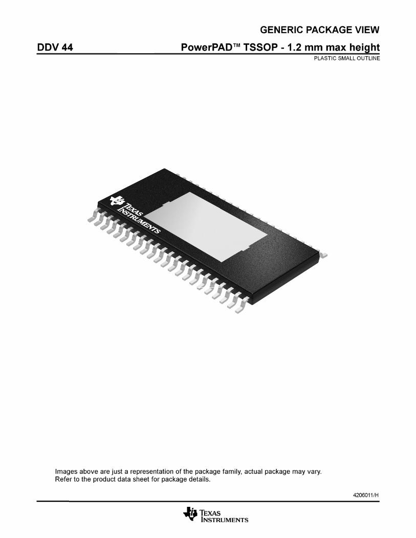
The thermal grease thermal resistance can be calculated from the exposed power pad or heat slug area and thethermal grease manufacturer's area thermal resistance (expressed in °C-in 2/W or °C-mm2/W). The approximateexposed heat slug size is as follows:• DRV8332, 44-pin DDV …… 0.055 in2 (35.6 mm 2)
The thermal resistance of a thermal pad is considered higher than a thin thermal grease layer and is notrecommended. Thermal tape has an even higher thermal resistance and should not be used at all. Heat sinkthermal resistance is predicted by the heat sink vendor, modeled using a continuous flow dynamics (CFD) model,or measured.
Thus the system RθJA = RθJC + thermal grease resistance + heat sink resistance.
See the TI application report, IC Package Thermal Metrics (SPRA953A), for more thermal information.
20 Submit Documentation Feedback Copyright © 2013–2014, Texas Instruments Incorporated
Product Folder Links: DRV8332-HT
DRV8332-HT
www.ti.com SLES274B –AUGUST 2013–REVISED JANUARY 2014
REVISION HISTORY
Changes from Revision A (September 2013) to Revision B Page
• Changed Overcurrent (OC) Protection section ................................................................................................................... 12• Deleted Overtemperature Protection section ...................................................................................................................... 13
Copyright © 2013–2014, Texas Instruments Incorporated Submit Documentation Feedback 21
Product Folder Links: DRV8332-HT
PACKAGE OPTION ADDENDUM
www.ti.com 31-Jan-2014
Addendum-Page 1
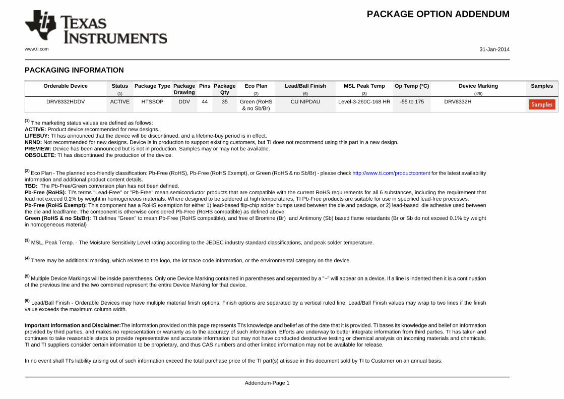
PACKAGING INFORMATION
Orderable Device Status(1)
Package Type PackageDrawing
Pins PackageQty
Eco Plan(2)
Lead/Ball Finish(6)
MSL Peak Temp(3)
Op Temp (°C) Device Marking(4/5)
Samples
DRV8332HDDV ACTIVE HTSSOP DDV 44 35 Green (RoHS& no Sb/Br)
CU NIPDAU Level-3-260C-168 HR -55 to 175 DRV8332H
(1) The marketing status values are defined as follows:ACTIVE: Product device recommended for new designs.LIFEBUY: TI has announced that the device will be discontinued, and a lifetime-buy period is in effect.NRND: Not recommended for new designs. Device is in production to support existing customers, but TI does not recommend using this part in a new design.PREVIEW: Device has been announced but is not in production. Samples may or may not be available.OBSOLETE: TI has discontinued the production of the device.
(2) Eco Plan - The planned eco-friendly classification: Pb-Free (RoHS), Pb-Free (RoHS Exempt), or Green (RoHS & no Sb/Br) - please check http://www.ti.com/productcontent for the latest availabilityinformation and additional product content details.TBD: The Pb-Free/Green conversion plan has not been defined.Pb-Free (RoHS): TI's terms "Lead-Free" or "Pb-Free" mean semiconductor products that are compatible with the current RoHS requirements for all 6 substances, including the requirement thatlead not exceed 0.1% by weight in homogeneous materials. Where designed to be soldered at high temperatures, TI Pb-Free products are suitable for use in specified lead-free processes.Pb-Free (RoHS Exempt): This component has a RoHS exemption for either 1) lead-based flip-chip solder bumps used between the die and package, or 2) lead-based die adhesive used betweenthe die and leadframe. The component is otherwise considered Pb-Free (RoHS compatible) as defined above.Green (RoHS & no Sb/Br): TI defines "Green" to mean Pb-Free (RoHS compatible), and free of Bromine (Br) and Antimony (Sb) based flame retardants (Br or Sb do not exceed 0.1% by weightin homogeneous material)
(3) MSL, Peak Temp. - The Moisture Sensitivity Level rating according to the JEDEC industry standard classifications, and peak solder temperature.
(4) There may be additional marking, which relates to the logo, the lot trace code information, or the environmental category on the device.
(5) Multiple Device Markings will be inside parentheses. Only one Device Marking contained in parentheses and separated by a "~" will appear on a device. If a line is indented then it is a continuationof the previous line and the two combined represent the entire Device Marking for that device.
(6) Lead/Ball Finish - Orderable Devices may have multiple material finish options. Finish options are separated by a vertical ruled line. Lead/Ball Finish values may wrap to two lines if the finishvalue exceeds the maximum column width.
Important Information and Disclaimer:The information provided on this page represents TI's knowledge and belief as of the date that it is provided. TI bases its knowledge and belief on informationprovided by third parties, and makes no representation or warranty as to the accuracy of such information. Efforts are underway to better integrate information from third parties. TI has taken andcontinues to take reasonable steps to provide representative and accurate information but may not have conducted destructive testing or chemical analysis on incoming materials and chemicals.TI and TI suppliers consider certain information to be proprietary, and thus CAS numbers and other limited information may not be available for release.
In no event shall TI's liability arising out of such information exceed the total purchase price of the TI part(s) at issue in this document sold by TI to Customer on an annual basis.
PACKAGE OPTION ADDENDUM
www.ti.com 31-Jan-2014
Addendum-Page 2
OTHER QUALIFIED VERSIONS OF DRV8332-HT :
• Catalog: DRV8332
NOTE: Qualified Version Definitions:
• Catalog - TI's standard catalog product
IMPORTANT NOTICE
Texas Instruments Incorporated and its subsidiaries (TI) reserve the right to make corrections, enhancements, improvements and otherchanges to its semiconductor products and services per JESD46, latest issue, and to discontinue any product or service per JESD48, latestissue. Buyers should obtain the latest relevant information before placing orders and should verify that such information is current andcomplete. All semiconductor products (also referred to herein as “components”) are sold subject to TI’s terms and conditions of salesupplied at the time of order acknowledgment.TI warrants performance of its components to the specifications applicable at the time of sale, in accordance with the warranty in TI’s termsand conditions of sale of semiconductor products. Testing and other quality control techniques are used to the extent TI deems necessaryto support this warranty. Except where mandated by applicable law, testing of all parameters of each component is not necessarilyperformed.TI assumes no liability for applications assistance or the design of Buyers’ products. Buyers are responsible for their products andapplications using TI components. To minimize the risks associated with Buyers’ products and applications, Buyers should provideadequate design and operating safeguards.TI does not warrant or represent that any license, either express or implied, is granted under any patent right, copyright, mask work right, orother intellectual property right relating to any combination, machine, or process in which TI components or services are used. Informationpublished by TI regarding third-party products or services does not constitute a license to use such products or services or a warranty orendorsement thereof. Use of such information may require a license from a third party under the patents or other intellectual property of thethird party, or a license from TI under the patents or other intellectual property of TI.Reproduction of significant portions of TI information in TI data books or data sheets is permissible only if reproduction is without alterationand is accompanied by all associated warranties, conditions, limitations, and notices. TI is not responsible or liable for such altereddocumentation. Information of third parties may be subject to additional restrictions.Resale of TI components or services with statements different from or beyond the parameters stated by TI for that component or servicevoids all express and any implied warranties for the associated TI component or service and is an unfair and deceptive business practice.TI is not responsible or liable for any such statements.Buyer acknowledges and agrees that it is solely responsible for compliance with all legal, regulatory and safety-related requirementsconcerning its products, and any use of TI components in its applications, notwithstanding any applications-related information or supportthat may be provided by TI. Buyer represents and agrees that it has all the necessary expertise to create and implement safeguards whichanticipate dangerous consequences of failures, monitor failures and their consequences, lessen the likelihood of failures that might causeharm and take appropriate remedial actions. Buyer will fully indemnify TI and its representatives against any damages arising out of the useof any TI components in safety-critical applications.In some cases, TI components may be promoted specifically to facilitate safety-related applications. With such components, TI’s goal is tohelp enable customers to design and create their own end-product solutions that meet applicable functional safety standards andrequirements. Nonetheless, such components are subject to these terms.No TI components are authorized for use in FDA Class III (or similar life-critical medical equipment) unless authorized officers of the partieshave executed a special agreement specifically governing such use.Only those TI components which TI has specifically designated as military grade or “enhanced plastic” are designed and intended for use inmilitary/aerospace applications or environments. Buyer acknowledges and agrees that any military or aerospace use of TI componentswhich have not been so designated is solely at the Buyer's risk, and that Buyer is solely responsible for compliance with all legal andregulatory requirements in connection with such use.TI has specifically designated certain components as meeting ISO/TS16949 requirements, mainly for automotive use. In any case of use ofnon-designated products, TI will not be responsible for any failure to meet ISO/TS16949.
Products ApplicationsAudio www.ti.com/audio Automotive and Transportation www.ti.com/automotiveAmplifiers amplifier.ti.com Communications and Telecom www.ti.com/communicationsData Converters dataconverter.ti.com Computers and Peripherals www.ti.com/computersDLP® Products www.dlp.com Consumer Electronics www.ti.com/consumer-appsDSP dsp.ti.com Energy and Lighting www.ti.com/energyClocks and Timers www.ti.com/clocks Industrial www.ti.com/industrialInterface interface.ti.com Medical www.ti.com/medicalLogic logic.ti.com Security www.ti.com/securityPower Mgmt power.ti.com Space, Avionics and Defense www.ti.com/space-avionics-defenseMicrocontrollers microcontroller.ti.com Video and Imaging www.ti.com/videoRFID www.ti-rfid.comOMAP Applications Processors www.ti.com/omap TI E2E Community e2e.ti.comWireless Connectivity www.ti.com/wirelessconnectivity
Mailing Address: Texas Instruments, Post Office Box 655303, Dallas, Texas 75265Copyright © 2016, Texas Instruments Incorporated