Embed Size (px)
Citation preview

REL 352 Version 1.13
This document has additional enhancements description in REL352 V 1.13 and REL352Acceptance Test:
Additional enhancements in REL 352 V 1.13:
1) Transient Block Logic
Transient blocking logic is added to the REL352 system logic diagram V1.12, Doc. No. 1358D80 as below:
PLT (pilot trip)
A2(ITA2)
4040
into Pilot Trip OR
TRBLINOUT'1'
COMM
'3'2540
'2'
The logic works as follows:
- Transient Blocking Logic doesn’t affect the pilot trip if the trip occurs within 25ms or 40ms following adisturbance. The assumption is that any internal fault will cause the correct trip in 25ms for FSK PLC and in40ms for ON/OFF PLC.
- In the blocking state, the blocking signal drop out timer starts counting down as soon as PLT (Pilot Trip) isasserted. It takes 40ms from the time PLT is asserted to the time the blocking is unarmed.
A new TRBL setting per default is set to “OUT”.
2) FD1T supervision of IKEY for FSK PLC schemes
FD1T supervision of IKEY for FSK PLC schemes is added to the REL352 system logic diagram V1.12, Doc. No.1358D80 as below:
IKO To IKEY OR
FDKS ΙΝ
OUT
COMM 2 3
IKEY
"1"
FD1T
A new setting FDKS is added with two options “IN” and “OUT” with default setting set “OUT”. The new setting isonly applicable for FSK PLS systems. When set to ON/OFF PLC, FD1T should always supervise the keying aspreviously.
3) Correction at page 14 in the I.L.40-201.9B:
2. Composite Sequence Filter Phase Comparison Current only systems, like the REL 352, compare the currents measured at the terminals of the transmission line.In a phase comparison system, like the REL 352, the phase relationship determines whether the condition isinternal or external.

REL 352 Version 1.13
For an internal fault, the currents are essentially "in phase" at the terminals of the transmission line. For anexternal fault; the currents are 180° out of phase. Figure 3-1 (page 22), illustrates the concept.
The REL 352 combines the phase current (lA, IB, and IC) measured at the protective relaying terminal into asingle quantity. This quantity is an output of Symmetrical Component Filter which is proportional to the weightedsum of the sequence components. Figure 3-2 (page 23), illustrates this filter.
The quantity IT, therefore, is defined as:
IT = C0I0 – C1I1 + C2I2 (3.1)
The Positive, Negative, and Zero sequence quantities are calculated from the sampled current data as follows:
)]()()([31)(0 kikikiki cba ++=
)]1( 732.1)( 2 )1( 732.1)()([31)(1 −+−−−+= kikikikikiki ccbba
)]1( 732.1)( )1( 732.1)( 2)([31)(2 −−+−+−= kikikikikiki ccbba
))(0())(2())(1( 021 kiCkiCkiCITIcomp kk ∗+∗+∗−==
The quantity IT is itself is normally a sine wave. The C1 (positive sequence weighting coefficient), C2 (negativesequence weighting coefficient) and C0 (zero sequence weighting coefficient) are system settings that control thesensitivity of the relaying system. For dynamic range considerations, the sequence filter has a saturationcharacteristic whereby the signal clamps at ± 160 √ 2 amps on a 5 amp rated ct system or ± 32 √2 ampsmaximum on a 1 amp rated ct system.
REL 352 Version 1.13
REL352 Acceptance TestThis document contains additions to Appendix I, Acceptance Test in the REL352 Instruction Leaflet, 40-201.9B,dated February 1999.
The following section replaces Section 1.6 in IL40-201.9B, page 139:
1.6 Functional Tests – Phase Comparison Differential System
The following section documents all the various types of tests that can be done to verify operating characteristicsof the REL352 relay. If a simple single unit test needs to be performed, sections 1.6.1 and 1.6.2 will be adequatefor verification purposes. Section 1.6.3 & 1.6.4 are included for lab type back to back verification tests and arenot necessary for field installation type testing.
1.6.1 Single unit loopback test – Internal Faults
Step 1. Enter the following settings:
FREQ = 60 IKEY = 0.75 IOM = 0.50RP = NO TERM = 2TRM TOG = BLKCTYP = 5 COMM = 3ST Z2P = 4.0CTR = 5000 CINT = BIO T2P = 0.10VTR = 7000 C0 = 0.00 Z2GF = 4.0OSC = TRIP C1 = 0.10 Z2GR = 2.0FDAT = TRIP C2 = 0.70 T2G = 0.1TRGG = 0.50 LDT1 = 0.0 Z3P = 7.0TRGP = 0.50 LDT2 = 0.0 T3P = 1.0CD = dI FDSK = OUT Z3GF = 7.0SFD1 = ITA1 TRBL = OUT Z3GR = 3.5SFD2 = ITA2 XPUD = 1.50 T3G = 1.0RBEN = ALRB DTYP = KM OST = WAY0UNBK = OUT PANG = 75 OSB = BOTHCNT = 1CNT GANG = 75 RT = 2.0ITA1 = 25% ZR = 3.0 RU = 4.0LP = 1.50 BKUP = OUT OST1 = 2.0ITA2 = 0.20 LOPB = NO OST2 = 3.0IPL = 0.50 FDOP = IN OST3 = 3.0IPH = OUT FDOG = IN OSOT = 100IGL = 0.50 DIRU = ZSEQ IT2T = 0IGH = OUT
Step 2. Power down the unit.
Step 3. Remove the inner chassis.
a) Note factory settings of jumpers on Interconnect and Opto-isolated Input modules. On the opto-isolatedInput module the default factory jumper settings are as: JMP1, JMP2, JMP3, JMP4, JMP5, JMP6 are setin position 1-2 corresponding to auxiliary voltage 15/20VDC. JMP7, JMP8, JMP9 are set in position 3-4corresponding to auxiliary voltage 48/125VDC. On the Interconnect module default factory jumper settingis as: JMP7 (selection of transmitter keying) is set in position 5-6 corresponding to auxiliary voltage15/20VDC.
b) Make sure that the jumpers, JMP1, JMP2, JMP3, JMP4, JMP5 and JMP6, JMP7, JMP8 and JMP9 on theOpto-isolated Input module and JMP7 on the Interconnect module are set for the desired battery voltage.

REL 352 Version 1.13
c) Set the following jumpers on the Interconnect module:
JMP1 Normal (Channel Fail)JMP4 Inverted (MARK 1)JMP5 Normal (SPACE 1)JMP6 Normal (Key Out)
Note that these are test settings and need to be changed to their proper position before the relay is putinto service.
Step 4. Insert and secure the inner chassis.
Step 5. Make the following connections on the rear of the REL352:
NOTE: Do not connect these connections to DC until the input buffer voltage settings have been completed instep 3.b.
Step 6.
a) Power the unit upb) Connect the battery as shown in diagram in step 5 above.
Step 7. Verify relays response to all types of relay faults by applying the test quantities per the following table.Note; apply all of the fault currents suddenly. Adjust value up or down to find the point where relay justtrips. Three different cases are presented, only one needs to be performed.
XMTR BAT (+)
XMTR KEY (+)
XMTR RETURN (-)
TB4 -11
TB4 -12
TB4 - 13
SPACE 1 (+)
MARK (+)
RCVR RETURN (-)
TB5 - 7
TB5 -8
TB5 - 10
DC (-)DC (+)
REL 352 Version 1.13
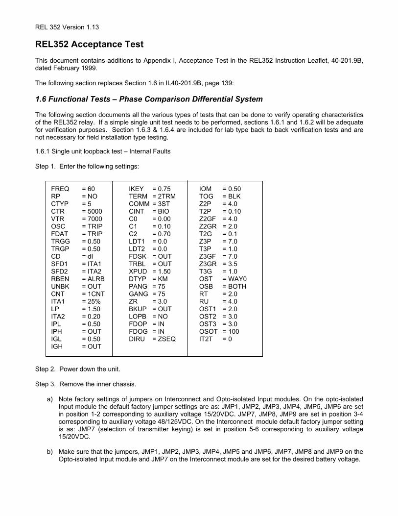
Test Conditions: Case 1 - C0=0, C1=0.1, C2=0.7, IKEY=0.75 & LP=1.50
TABLE 1
Fault Type IAmps ∠ Angle
CalculatedPickup Value
CurrentPickup range
AG IA = 7.30 ∠ 0
IB = 0 ∠ -120IC = 0 ∠ -240
7.30A 6.6A – 8.0A
BG IA = 0 ∠ 0
IB = 6.05 ∠ -120IC = 0 ∠ -240
6.05A 5.4A – 6.7A
CG IA = 0 ∠ 0
IB = 0 ∠ -120IC = 6.05 ∠ -240
6.05A 5.4A – 6.7A
AB IA = 4.06 ∠ 0
IB = 4.06 ∠ -180IC = 0 ∠ -240
4.06A 3.7A – 4.5A
BC IA = 0 ∠ 0
IB = 3.28 ∠ -120IC = 3.28 ∠ -300
3.28A 2.9A – 3.6A
CA IA = 4.06 ∠ -60
IB = 0 ∠ -120IC = 4.06 ∠ -240
4.06A 3.7A – 4.5A
ABG IA = 5.08 ∠ 0
IB = 5.08 ∠ -150IC = 0 ∠ -240
5.08A 4.6A – 5.6A
BCG IA = 0 ∠ 0
IB = 3.83 ∠ -120IC = 3.83 ∠ -270
3.83A 3.4A – 4.2A
CAG IA = 5.08 ∠ -30
IB = 0 ∠ -120IC = 5.08 ∠ -240
5.08A 4.6A – 5.6A
ABC IA = 14.55 ∠ 0
IB = 14.55 ∠ -120IC = 14.55 ∠ -240
14.55A 13.0A – 16.0A
REL 352 Version 1.13
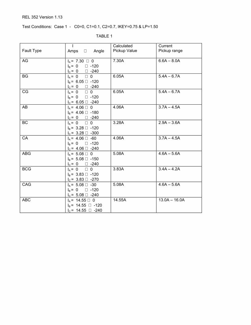
Test Conditions: Case 2 - C0=1, C1=0.1, C2=0.7, IKEY=0.75 & LP=1.50
TABLE 2
Fault Type IAmps ∠ Angle
CalculatedPickup Value
CurrentPickup range
AG IA = 2.73 ∠ 0
IB = 0 ∠ -120IC = 0 ∠ -240
2.73A 2.4A –3.0A
BG IA = 0 ∠ 0
IB = 4.5 ∠ -120IC = 0 ∠ -240
4.5A 4.0A –4.9A
CG IA = 0 ∠ 0
IB = 0 ∠ -120IC = 4.5 ∠ -240
4.5A 4.0A – 4.9A
AB IA = 3.84 ∠ 0
IB = 3.84 ∠ -180IC = 0 ∠ -240
3.84A 3.4A – 4.2A
BC IA = 0 ∠ 0
IB = 3.15 ∠ -120IC = 3.15 ∠ -300
3.15A 2.8A – 3.5A
CA IA = 3.84 ∠ -60
IB = 0 ∠ -120IC = 3.84 ∠ -240
3.84A 3.4A – 4.2A
ABG IA = 6.29 ∠ 0
IB = 6.29 ∠ -150IC = 0 ∠ -240
6.29A 5.6 A – 6.9A
BCG IA = 0 ∠ 0
IB = 2.57 ∠ -120IC = 2.57 ∠ -270
2.57A 2.3A – 2.8A
CAG IA = 6.29 ∠ -30
IB = 0 ∠ -120IC = 6.29 ∠ -240
6.29A 5.6A – 6.9A
ABC IA = 14.55 ∠ 0
IB = 14.55 ∠ -120IC = 14.55 ∠ -240
14.55A 13.0 – 16.0A

REL 352 Version 1.13
Test Conditions: Case 3 - C0=2.5, C1=0.1, C2=0.7, IKEY=0.75 & LP=1.50
TABLE 3
Fault Type IAmps ∠ Angle
CalculatedPickup Value
CurrentPickup range
AG IA = 1.41 ∠ 0
IB = 0 ∠ -120IC = 0 ∠ -240
1.41A 1.3A – 1.6A
BG IA = 0 ∠ 0
IB = 1.91 ∠ -120IC = 0 ∠ -240
1.91A 1.7A – 2.1A
CG IA = 0 ∠ 0
IB = 0 ∠ -120IC = 1.91 ∠ -240
1.91A 1.7A – 2.1A
AB IA = 3.87 ∠ 0
IB = 3.87 ∠ -180IC = 0 ∠ -240
3.87A 3.5A – 4.3A
BC IA = 0 ∠ 0
IB = 3.28 ∠ -120IC = 3.28 ∠ -300
3.28A 2.9A – 3.6A
CA IA = 3.87 ∠ -60
IB = 0 ∠ -120IC = 3.87 ∠ -240
3.87A 3.5A – 4.3A
ABG IA = 4.50 ∠ 0
IB = 4.50 ∠ -150IC = 0 ∠ -240
4.50A 4.05A – 4.9A
BCG IA = 0 ∠ 0
IB = 1.84 ∠ -120IC = 1.84 ∠ -270
1.84A 1.6A – 2.0A
CAG IA = 4.50 ∠ -30
IB = 0 ∠ -120IC = 4.50 ∠ -240
4.50A 4.05A – 4.9A
ABC IA = 14.55 ∠ 0
IB = 14.55 ∠ -120IC = 14.55 ∠ -240
14.55A 13.0A – 16.0A

REL 352 Version 1.13
1.6.2 Single unit loop-back test – External Faults
To verify that the relay does not trip for external faults, perform the following steps.
Step 1. Shut off DC to the relay and remove the inner chassis.
Step 2. Set jumper JMP4 to Normal & JMP5 to Inverted on the interconnect module. This simulates an externalfault since the received MARK & SPACE signals are opposite in polarity from the LP & LN signals.
Step 3. Insert and secure the inner chassis
Step 4. Power the unit up.
Step 5. Apply faults from tables 1, 2 or 3 to verify that the relay does not trip for current values above the previoustrip points.
1.6.3 Dual unit back to back tests – External Faults
Step 1. To test the relays back to back several connections need to be made. Hook up the relays as follows:
Communications connections
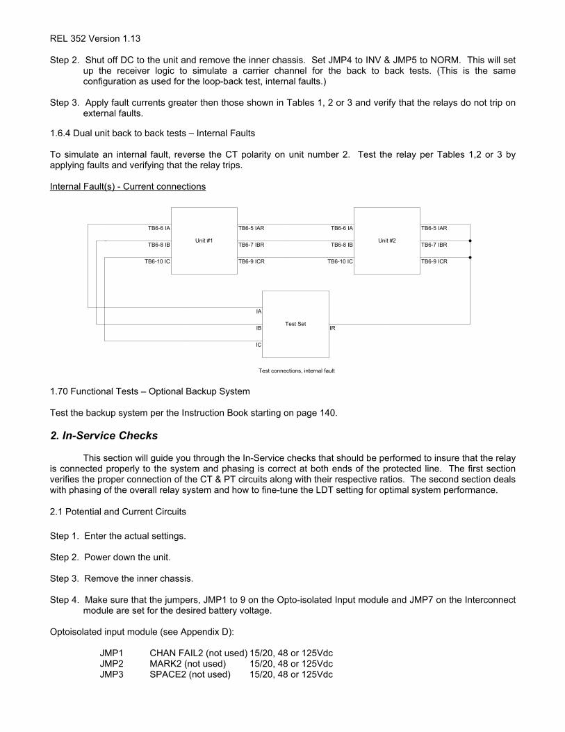
External Fault(s) - Current connections
XMIT BAT (+)
XMIT KEY (+)
XMTR RETURN (-)
SPACE1 (+)
MARK1 (+)
RCVR RETURN (-)
TB4 - 11
TB4 - 12
TB4 - 13
TB5 - 7
TB5 - 8
TB5 - 10
REL352 Unit #1 REL352 Unit #2
TB4 - 11
TB4 - 12
TB4 - 13
TB5 - 7
TB5 - 8
TB5 - 10
XMIT BAT (+)
XMIT KEY (+)
XMTR RETURN (-)
SPACE1 (+)
MARK1 (+)
RCVR RETURN (-)
DC (-)DC (+)
Unit #1
TB6-6 IA
TB6-8 IB
TB6-10 IC
TB6-5 IAR
TB6-7 IBR
TB6-9 ICR
Unit #2
TB6-5 IAR
TB6-7 IBR
TB6-9 ICR
TB6-6 IA
TB6-8 IB
TB6-10 IC
Test Set
IA
IB
IC
IR
Test connections, external fault
REL 352 Version 1.13
Step 2. Shut off DC to the unit and remove the inner chassis. Set JMP4 to INV & JMP5 to NORM. This will setup the receiver logic to simulate a carrier channel for the back to back tests. (This is the sameconfiguration as used for the loop-back test, internal faults.)
Step 3. Apply fault currents greater then those shown in Tables 1, 2 or 3 and verify that the relays do not trip onexternal faults.
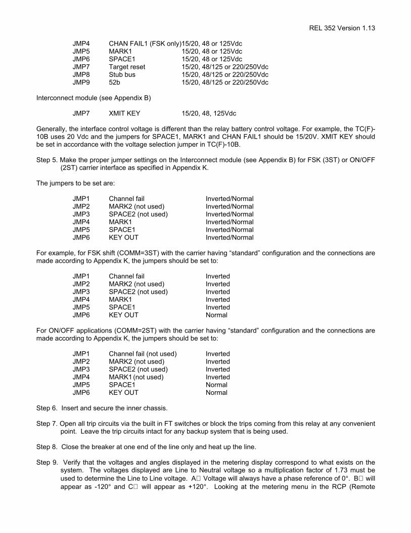
1.6.4 Dual unit back to back tests – Internal Faults
To simulate an internal fault, reverse the CT polarity on unit number 2. Test the relay per Tables 1,2 or 3 byapplying faults and verifying that the relay trips.
Internal Fault(s) - Current connections
1.70 Functional Tests – Optional Backup System
Test the backup system per the Instruction Book starting on page 140.
2. In-Service Checks
This section will guide you through the In-Service checks that should be performed to insure that the relayis connected properly to the system and phasing is correct at both ends of the protected line. The first sectionverifies the proper connection of the CT & PT circuits along with their respective ratios. The second section dealswith phasing of the overall relay system and how to fine-tune the LDT setting for optimal system performance.
2.1 Potential and Current Circuits Step 1. Enter the actual settings.
Step 2. Power down the unit.
Step 3. Remove the inner chassis.
Step 4. Make sure that the jumpers, JMP1 to 9 on the Opto-isolated Input module and JMP7 on the Interconnectmodule are set for the desired battery voltage.
Optoisolated input module (see Appendix D):
JMP1 CHAN FAIL2 (not used) 15/20, 48 or 125VdcJMP2 MARK2 (not used) 15/20, 48 or 125VdcJMP3 SPACE2 (not used) 15/20, 48 or 125Vdc
Unit #1
TB6-6 IA
TB6-8 IB
TB6-10 IC
TB6-5 IAR
TB6-7 IBR
TB6-9 ICR
Unit #2
TB6-6 IA
TB6-8 IB
TB6-10 IC
TB6-5 IAR
TB6-7 IBR
TB6-9 ICR
Test Set
IA
IB
IC
IR
Test connections, internal fault
REL 352 Version 1.13
JMP4 CHAN FAIL1 (FSK only)15/20, 48 or 125VdcJMP5 MARK1 15/20, 48 or 125VdcJMP6 SPACE1 15/20, 48 or 125VdcJMP7 Target reset 15/20, 48/125 or 220/250VdcJMP8 Stub bus 15/20, 48/125 or 220/250VdcJMP9 52b 15/20, 48/125 or 220/250Vdc
Interconnect module (see Appendix B)
JMP7 XMIT KEY 15/20, 48, 125Vdc
Generally, the interface control voltage is different than the relay battery control voltage. For example, the TC(F)-10B uses 20 Vdc and the jumpers for SPACE1, MARK1 and CHAN FAIL1 should be 15/20V. XMIT KEY shouldbe set in accordance with the voltage selection jumper in TC(F)-10B.
Step 5. Make the proper jumper settings on the Interconnect module (see Appendix B) for FSK (3ST) or ON/OFF(2ST) carrier interface as specified in Appendix K.
The jumpers to be set are:
JMP1 Channel fail Inverted/NormalJMP2 MARK2 (not used) Inverted/NormalJMP3 SPACE2 (not used) Inverted/NormalJMP4 MARK1 Inverted/NormalJMP5 SPACE1 Inverted/NormalJMP6 KEY OUT Inverted/Normal
For example, for FSK shift (COMM=3ST) with the carrier having “standard” configuration and the connections aremade according to Appendix K, the jumpers should be set to:
JMP1 Channel fail InvertedJMP2 MARK2 (not used) InvertedJMP3 SPACE2 (not used) InvertedJMP4 MARK1 InvertedJMP5 SPACE1 InvertedJMP6 KEY OUT Normal
For ON/OFF applications (COMM=2ST) with the carrier having “standard” configuration and the connections aremade according to Appendix K, the jumpers should be set to:
JMP1 Channel fail (not used) InvertedJMP2 MARK2 (not used) InvertedJMP3 SPACE2 (not used) InvertedJMP4 MARK1 (not used) InvertedJMP5 SPACE1 NormalJMP6 KEY OUT Normal
Step 6. Insert and secure the inner chassis.
Step 7. Open all trip circuits via the built in FT switches or block the trips coming from this relay at any convenientpoint. Leave the trip circuits intact for any backup system that is being used.
Step 8. Close the breaker at one end of the line only and heat up the line.
Step 9. Verify that the voltages and angles displayed in the metering display correspond to what exists on the
system. The voltages displayed are Line to Neutral voltage so a multiplication factor of 1.73 must beused to determine the Line to Line voltage. A∅ Voltage will always have a phase reference of 0°. B∅ willappear as -120° and C∅ will appear as +120°. Looking at the metering menu in the RCP (Remote

REL 352 Version 1.13
Communication Program), all of the Voltages, Currents and Angles are displayed, as well as Positive,Negative and zero sequence values. If the PT circuits are hooked up correctly, all of the potential shouldappear as Positive Sequence or V1. Small quantities of V2 & V0 are acceptable and are a result of smallphase unbalances in the system and or variations in the PT’s themselves. Verify at both ends and recordthe data.
Step 10. Close the breaker in at the remote end.
Step 11. Verify that the current levels and angles displayed in the metering display correspond to what is actually
flowing in the system. This is more easily done in the metering menu of RCP. Verify with the LoadDispatcher current levels and power flow. Verify that the relay sees the same direction and same relativevalue of power flow as the Load dispatcher. If not the CT’s may be hooked up backwards or the CT ratioentered in the settings is incorrect. When power is flowing out of station “A”, it will appear as (+) watts inthe metering menu. Station “B” will see this same power flow coming in, and it will appear as (-) watts.The current angles at station “B” will also be 180° out of phase with the angles at station “A”.
Step 12. Record and compare the current levels and angles with the levels and angles at the other end of the
line. Verify that the angles in all three phases are 180° different from one end to the other. Also verify inthe RCP metering menu that the Current appears as mainly I1 or positive sequence current. This willverify that the phase rotation is correct at both ends
Step 13. After all checks of Voltage & Current are completed and everything corresponds with what the Load
Dispatcher is reporting, you are ready to move on to the phase comparison section of the test. Ifproblems exist, they must be corrected before moving on to the phase comparison checks.
2.2 Phase Comparison Checks
The phase comparison checks will utilize load current to verify proper phase relationships at both ends of the line.In order to facilitate this check, the settings of C0, C1, C2, LP & IKEY will be changed to values that willcorrespond to the levels of I1 in the system, and make the relay respond as if it was seeing an external fault. Inorder to do these tests, the OSCAR & RCP programs must be used to process and view the Oscillographicrecords.
Step 1. To set this up properly, change the settings in the relay to the following, after first recording what theactual settings are:
C0=0C2=0IKEY=0.75LP=1.5
The value of C1 is calculated based on the actual load current. Note the value of A∅ current (assuming 3∅balanced load), then calculate the value of C1 by the formula C1=(1.5/IA) +0.1. These values will cause the relayto key at both ends and begin phase comparison. The value of C1 is calculated to be slightly above the LPsetting of 1.5 to insure the relay is keyed and in phase comparison. These settings must be the same andapplied at both ends (CT ratios are the same at each line end).
Step 2. Use the Display Select button to scroll down to the test menu on the front of the REL352. Use the Raisebutton to scroll to move through the functions until “Test” appears in the window. With a pencil or pen,trigger an Oscillographic record by depressing the “Enter” key on the front of the relay. Make sure youget a green “Value Accepted” led indication.
Step 3. In the RCP relay menu, go to Oscillographic Data <enter>. Select Analog and Digital data <enter>.Select record 0 (most recent)<enter>. Wait for the program to download the 48 records then save thisrecord to a file in a subdirectory of your choice.

REL 352 Version 1.13
Step 4. Open the OSCAR program. Select Osc Data File <enter>. Select REL352 <enter>. Find the .oph fileyou saved in step 3 <enter>. Wait for the OSCAR program to calculate the analog and digital data in thesaved file.
Step 5. Select Graph Osc Data <enter>. Now you will see the analog and digital data associated with thisrecord. The waveforms of particular interest are M1, S1, LP1, LN1, COIN & PLT. M1 & S1 shouldappear as a series of square waves with no overlap of the rising and falling edges. LP1 & LN1 shouldalso appear as square waves with no overlap in the rising and falling edges. For an external fault, (this iswhat we are simulating) the positive going waveform of LN1 should “nest” in the negative goingwaveform of S1 as follows:
S1 & M1
LN1 & LP1
LP1 positive pulse should also “nest” in the negative going pulses of M1.
Step 6. If you have these waveforms you’re almost done! It verifies that the communication channel is workingand the phasing of the carrier Mark & Space signals is correct. If you don’t get any waveforms at all,check the setting of IPL and IPG and make sure that they are low enough to be triggered by the amountof load current flowing. If they are set low, then check to make sure the communication channel isworking properly. If you do have LN1 & S1 waveforms, but they do not “nest” and you have COIN & PLToutput waveforms, then the polarity of the input signals are most likely reversed. Check the settings ofJMP4 & JMP5 on the interconnect module as per 2.1 Potential and Current circuits, step 5. If the jumpersettings are OK at both line ends, then check CT polarity.
Step 7. Next check the amount of time between the rising edge of LN1and falling edge of S1. Subtract the valueof LN1 from S1 then divide by 2. This will give you the value of LDT that you need to enter in the mainsettings. Go back to Step 2, trigger a record and do it all over again. Verify on the new record that theLN1 is centered in the S1 waveform. If it is, you’re done! If not, measure the time on both sides of LN1and adjust the LDT to center the waveform.
Step 8. If all the phasing is done correctly, the nesting should be centered and there should be little or no COINoutput. This waveform is the Coincidence output that will trigger a trip. COIN needs to be greater then 4ms before a PLT output is possible, so if you do have a little COIN output less then 1-2 ms wide, it’s ok.
Step 9. Verify at both ends.
Step 10. Return C0, C1, C2, IKEY, and LP back to normal at both ends.
Step 11. Scroll to the TEST menu on the front of the REL352. Next scroll through the functions until the TLDTfunction is displayed. This is the automatic LDT metering function and it should be very close to whatwas set for LDT in step 7. If it is different from what you set, go with the value that you obtained in step 7.Next scroll to the SRT function. It must be "NO”. This function stands for Standing Relay Trip. If this is“YES”, it means as soon as you close in the trip circuits you will trip the breaker!
Step 12. As a final step, go to the metering menu in RCP and take a snapshot of the As Left / In-Service values.To do this get into the metering screen then with the values displayed press <alt><F> to open the “file”window box, then <enter> again to “Save Screen”. This will save the screen in whatever menu you choseas a record of the In-Service values. It’s not a bad idea as well to go to the setting screen and take asnapshot there as well.
ABB Automation, Inc.Substation Automation & Protection DivisionCoral Springs, FLAllentown, PA
Instruction Leaflet
Effective: February, 1999Supersedes 40-201.9Adated March, 1998
REL 352 Version 1.12
Numerical Phase ComparisonTransmission Line ProtectionSystem
40-201.9B
ABB Network Partner

Power Automation and Protection Division I.L. 40-201.9B
! ATTENTION
It is recommended that the user of REL 352 equipment become acquainted with the information in this instruc-tion leaflet before energizing the system. Failure to do so may result in injury to personnel or damage to theequipment, and may affect the equipment warranty. If the REL 352 relay system is mounted in a cabinet, thecabinet must be bolted to the floor, or otherwise secured before REL 352 installation, to prevent the system fromtipping over.All integrated circuits used on the modules are sensitive to and can be damaged by the discharge of static elec-tricity. Electrostatic discharge precautions should be observed when handling modules or individualcomponents.
ABB does not assume liability arising out of the application or use of any product or circuit described herein.ABB reserves the right to make changes to any products herein to improve reliability, function or design. Spec-ifications and information herein are subject to change without notice. All possible contingencies which mayarise during installation, operation, or maintenance, and all details and variations of this equipment do not pur-port to be covered by these instructions. If further information is desired by purchaser regarding a particular in-stallation, operation or maintenance of equipment, the local ABB representative should be contacted.
© CopyrightABB Power T&D Company Inc.Published 1996, 1997, 1998, 1999All Rights reserved
ABB does not convey any license under its patent rights nor the rights of others.
i REL 352 Version 1.12
Trademarks
All terms mentioned in this book that are known to be trademarks or service marks are listed below. In addition,terms suspected of being trademarks or service marks have been appropriately capitalized. ABB Power T&D Com-pany Inc. cannot attest to the accuracy of this information. Use of a term in this book should not be regarded asaffecting the validity of any trademark or service mark.
IBM and PCare registered trademarks of the International Business Machines Corporation.WRELCOM is the registered trademark of the ABB Power T&D Company Inc.INCOM is the registered trademark of the Westinghouse Electric Corporation

I.L. 40-201.9B Power Automation and Protection Division
Equipment Identification
The REL 352 equipment is identified by the Catalog Number on the REL 352 chassis nameplate. The CatalogNumber can be decoded by using Catalog Number (see Section 3, pg. 3-26).
Production Changes
When engineering and production changes are made to the REL 352 equipment, a revision notation (Sub #) isreflected on the appropriate schematic diagram, and associated parts information.
Equipment Repair
Repair work is done most satisfactorily at the factory. When returning equipment, carefully pack modules andother units, etc. All equipment should be returned in the original packing containers if possible. Any damage dueto improperly packed items will be charged to the customer.
Document Overview
Section 1 provides the Product Description. Section 2 provides Specifications and External Connections. Sec-tion 3 presents applications with related Catalog Numbers for ordering purposes. Installation, Operation andMaintenance are described in Section 4, with related Setting Calculations in Section 5. Appendices A thru Hinclude related module circuit descriptions. Acceptance Tests are described in Appendix I. Computer Commu-nications are described in Appendix J, Application Notes in Appendix K, and Systems Diagrams are included inAppendix L.
Contents of Relay System
The REL 352 Relay System includes the style numbers, listed below, for each module.
Module Style
• Backplane - - - - - - - - - - - 1611C26 • Microprocessor - - - - - - 1611C22(Sub-Backplane Xfmr) - - - - - 1502B38 • Display - - - - - - - - - - 1498B40
• Interconnect - - - - - - - - - - 1618C45 • Power Supply - - - - - - - 1611C24
• Relay Output - - - - - - - - - - 1611C27 • Analog Input - - - - - - - - 1611C23
• Optoisolated Input - - - - - - - 1618C38
REL 352 Version 1.12 ii
iii REL 352 Version 1.12
Power Automation and Protection Division I.L. 40-201.9B
TABLE
CONTENTS
OF
PRODUCT DESCRIPTION 1
SPECIFICATIONS 2
APPLICATIONS & ORDERINGINFORMATION 3
INSTALLATION, OPERATION &MAINTENANCE 4
SETTING CALCULATIONS 5
BACKPLANE MODULE A
INTERCONNECT MODULE B
RELAY OUTPUT MODULE C
OPTOISOLATED INPUT MODULE D
MICROPROCESSOR MODULE E
DISPLAY MODULE F
POWER SUPPLY MODULE G
ANALOG INPUT MODULE H
ACCEPTANCE TESTS I
COMPUTER COMMUNICATIONS J
APPLICATION NOTES K
SYSTEM DIAGRAMS L

REL 352 Version 1.12 iv
I.L. 40-201.9B Power Automation and Protection Division
THIS PAGE RESERVED FOR NOTES
v REL 352 Version 1.12
Power Automation and Protection Division I.L. 40-201.9B
Table of Contents
Section 1 PRODUCT DESCRIPTION
1 INTRODUCTION- - - - - - - - - - - - - - - - - - - - - - - - - - - - - - - - - - - - - - - - - - - - - - - - - - - - - - - - - - - - - 1
2 REL 352 CONSTRUCTION - - - - - - - - - - - - - - - - - - - - - - - - - - - - - - - - - - - - - - - - - - - - - - - - - - - - - 1
3 REL 352 MODULES - - - - - - - - - - - - - - - - - - - - - - - - - - - - - - - - - - - - - - - - - - - - - - - - - - - - - - - - - - 1
3.1 Backplane Module - - - - - - - - - - - - - - - - - - - - - - - - - - - - - - - - - - - - - - - - - - - - - - - - - - - - - - - - - - - -2
3.2 Interconnect Module- - - - - - - - - - - - - - - - - - - - - - - - - - - - - - - - - - - - - - - - - - - - - - - - - - - - - - - - - - -2
3.3 Relay Output Module - - - - - - - - - - - - - - - - - - - - - - - - - - - - - - - - - - - - - - - - - - - - - - - - - - - - - - - - - -2
3.4 Optoisolated Input Module - - - - - - - - - - - - - - - - - - - - - - - - - - - - - - - - - - - - - - - - - - - - - - - - - - - - - -2
3.5 Microprocessor Module - - - - - - - - - - - - - - - - - - - - - - - - - - - - - - - - - - - - - - - - - - - - - - - - - - - - - - - -3
3.6 Display Module - - - - - - - - - - - - - - - - - - - - - - - - - - - - - - - - - - - - - - - - - - - - - - - - - - - - - - - - - - - - - -3
3.7 Power Supply Module - - - - - - - - - - - - - - - - - - - - - - - - - - - - - - - - - - - - - - - - - - - - - - - - - - - - - - - - -3
3.8 Analog Input Module - - - - - - - - - - - - - - - - - - - - - - - - - - - - - - - - - - - - - - - - - - - - - - - - - - - - - - - - - -4
3.9 Contact Outputs- - - - - - - - - - - - - - - - - - - - - - - - - - - - - - - - - - - - - - - - - - - - - - - - - - - - - - - - - - - - - -4
4 SELF-CHECKING SOFTWARE - - - - - - - - - - - - - - - - - - - - - - - - - - - - - - - - - - - - - - - - - - - - - - - - - - 4
5 UNIQUE REMOTE COMMUNICATION (WRELCOM) PROGRAM - - - - - - - - - - - - - - - - - - - - - - - - - - 5
Section 2 REL 352 SPECIFICATIONS
1 TECHNICAL - - - - - - - - - - - - - - - - - - - - - - - - - - - - - - - - - - - - - - - - - - - - - - - - - - - - - - - - - - - - - - - - 9
2 EXTERNAL CONNECTIONS - - - - - - - - - - - - - - - - - - - - - - - - - - - - - - - - - - - - - - - - - - - - - - - - - - - - 9
3 CONTACT DATA - - - - - - - - - - - - - - - - - - - - - - - - - - - - - - - - - - - - - - - - - - - - - - - - - - - - - - - - - - - 10
4 COMMUNICATION EQUIPMENT INTERFACE - - - - - - - - - - - - - - - - - - - - - - - - - - - - - - - - - - - - - - 10
5 OPTIONAL COMPUTER/NETWORK INTERFACE- - - - - - - - - - - - - - - - - - - - - - - - - - - - - - - - - - - - 10
6 CHASSIS DIMENSIONS AND WEIGHT - - - - - - - - - - - - - - - - - - - - - - - - - - - - - - - - - - - - - - - - - - - 10
7 ENVIRONMENTAL DATA - - - - - - - - - - - - - - - - - - - - - - - - - - - - - - - - - - - - - - - - - - - - - - - - - - - - - 11
REL 352 Version 1.12 vi
I.L. 40-201.9B Power Automation and Protection Division
Section 3 APPLICATIONS AND ORDERING INFORMATION
1 INTRODUCTION- - - - - - - - - - - - - - - - - - - - - - - - - - - - - - - - - - - - - - - - - - - - - - - - - - - - - - - - - - - - -13
2 COMPOSITE SEQUENCE FILTER PHASE COMPARISON - - - - - - - - - - - - - - - - - - - - - - - - - - - - - -14
2.1 Local Positive (LP) and Local Negative (LN) - - - - - - - - - - - - - - - - - - - - - - - - - - - - - - - - - - - - - - - - 15
2.2 IKEY - - - - - - - - - - - - - - - - - - - - - - - - - - - - - - - - - - - - - - - - - - - - - - - - - - - - - - - - - - - - - - - - - - - - 15
3 FSK POWER LINE CARRIER AND AUDIO TONE APPLICATIONS - - - - - - - - - - - - - - - - - - - - - - - -15
4 ON-OFF POWER LINE CARRIER APPLICATIONS - - - - - - - - - - - - - - - - - - - - - - - - - - - - - - - - - - - -15
5 THREE TERMINAL APPLICATIONS - - - - - - - - - - - - - - - - - - - - - - - - - - - - - - - - - - - - - - - - - - - - - -16
6 PILOT TRIP LOGIC- - - - - - - - - - - - - - - - - - - - - - - - - - - - - - - - - - - - - - - - - - - - - - - - - - - - - - - - - - -16
7 DIRECTIONAL OVERCURRENT UNITS- - - - - - - - - - - - - - - - - - - - - - - - - - - - - - - - - - - - - - - - - - - -17
8 OPTIONAL BACK-UP - - - - - - - - - - - - - - - - - - - - - - - - - - - - - - - - - - - - - - - - - - - - - - - - - - - - - - - - -17
8.1 Distance Relaying - - - - - - - - - - - - - - - - - - - - - - - - - - - - - - - - - - - - - - - - - - - - - - - - - - - - - - - - - - 17
8.2 Single Phase-to-Ground - - - - - - - - - - - - - - - - - - - - - - - - - - - - - - - - - - - - - - - - - - - - - - - - - - - - - - 18
8.3 Three-phase - - - - - - - - - - - - - - - - - - - - - - - - - - - - - - - - - - - - - - - - - - - - - - - - - - - - - - - - - - - - - - 18
8.4 Phase-to-Phase - - - - - - - - - - - - - - - - - - - - - - - - - - - - - - - - - - - - - - - - - - - - - - - - - - - - - - - - - - - - 19
8.5 Zone 2 and Zone 3 Distance Relaying - - - - - - - - - - - - - - - - - - - - - - - - - - - - - - - - - - - - - - - - - - - - 19
9 MISCELLANEOUS FUNCTIONS - - - - - - - - - - - - - - - - - - - - - - - - - - - - - - - - - - - - - - - - - - - - - - - - -20
9.1 Out-of-Step Trip (OST) and Out-of-Step Block (OSB) Logic - - - - - - - - - - - - - - - - - - - - - - - - - - - - - 20
9.2 Loss of Potential (LOPB)- - - - - - - - - - - - - - - - - - - - - - - - - - - - - - - - - - - - - - - - - - - - - - - - - - - - - - 20
9.3 Loss of Current (LOI) - - - - - - - - - - - - - - - - - - - - - - - - - - - - - - - - - - - - - - - - - - - - - - - - - - - - - - - - 20
10 RECLOSING LOGIC - - - - - - - - - - - - - - - - - - - - - - - - - - - - - - - - - - - - - - - - - - - - - - - - - - - - - - - - - -21
11 FAULT LOCATOR- - - - - - - - - - - - - - - - - - - - - - - - - - - - - - - - - - - - - - - - - - - - - - - - - - - - - - - - - - - -21
Section 4 OPERATION AND MAINTENANCE
1 SEPARATING THE INNER AND OUTERCHASSIS - - - - - - - - - - - - - - - - - - - - - - - - - - - - - - - - - - - -37
2 EXTERNAL WIRING - - - - - - - - - - - - - - - - - - - - - - - - - - - - - - - - - - - - - - - - - - - - - - - - - - - - - - - - - -37

vii REL 352 Version 1.12
Power Automation and Protection Division I.L. 40-201.9B
3 REL 352 FRONT PANEL DISPLAY- - - - - - - - - - - - - - - - - - - - - - - - - - - - - - - - - - - - - - - - - - - - - - - 38
3.1 Vacuum Fluorescent Display- - - - - - - - - - - - - - - - - - - - - - - - - - - - - - - - - - - - - - - - - - - - - - - - - - - -38
3.2 Indicators - - - - - - - - - - - - - - - - - - - - - - - - - - - - - - - - - - - - - - - - - - - - - - - - - - - - - - - - - - - - - - - - -38
3.3 Key Switches- - - - - - - - - - - - - - - - - - - - - - - - - - - - - - - - - - - - - - - - - - - - - - - - - - - - - - - - - - - - - - -39
4 FRONT PANEL OPERATION- - - - - - - - - - - - - - - - - - - - - - - - - - - - - - - - - - - - - - - - - - - - - - - - - - - 39
4.1 Settings Mode - - - - - - - - - - - - - - - - - - - - - - - - - - - - - - - - - - - - - - - - - - - - - - - - - - - - - - - - - - - - - -39
4.2 Metering (Volts/Amps/Angle) Mode - - - - - - - - - - - - - - - - - - - - - - - - - - - - - - - - - - - - - - - - - - - - - - -40
4.3 Target (Last And Previous Fault) Mode - - - - - - - - - - - - - - - - - - - - - - - - - - - - - - - - - - - - - - - - - - - -40
4.4 Test Mode Function - - - - - - - - - - - - - - - - - - - - - - - - - - - - - - - - - - - - - - - - - - - - - - - - - - - - - - - - - -41
5 JUMPER CONTROL - - - - - - - - - - - - - - - - - - - - - - - - - - - - - - - - - - - - - - - - - - - - - - - - - - - - - - - - - 45
5.1 Backplane Module - - - - - - - - - - - - - - - - - - - - - - - - - - - - - - - - - - - - - - - - - - - - - - - - - - - - - - - - - - -45
5.2 Optoisolated Input module - - - - - - - - - - - - - - - - - - - - - - - - - - - - - - - - - - - - - - - - - - - - - - - - - - - - -45
5.4 Interconnect Module- - - - - - - - - - - - - - - - - - - - - - - - - - - - - - - - - - - - - - - - - - - - - - - - - - - - - - - - - -46
5.5 Microprocessor Module - - - - - - - - - - - - - - - - - - - - - - - - - - - - - - - - - - - - - - - - - - - - - - - - - - - - - - -46
6 NETWORK INTERFACE - - - - - - - - - - - - - - - - - - - - - - - - - - - - - - - - - - - - - - - - - - - - - - - - - - - - - - 47
7 OSCILLOGRAPHIC DATA - - - - - - - - - - - - - - - - - - - - - - - - - - - - - - - - - - - - - - - - - - - - - - - - - - - - - 47
8 REL 352 SETTINGS - - - - - - - - - - - - - - - - - - - - - - - - - - - - - - - - - - - - - - - - - - - - - - - - - - - - - - - - - 47
9 MONITORING FUNCTIONS- - - - - - - - - - - - - - - - - - - - - - - - - - - - - - - - - - - - - - - - - - - - - - - - - - - - 48
10 TARGET (FAULT DATA) INFORMATION - - - - - - - - - - - - - - - - - - - - - - - - - - - - - - - - - - - - - - - - - - 48
11 ROUTINE VISUAL INSPECTION - - - - - - - - - - - - - - - - - - - - - - - - - - - - - - - - - - - - - - - - - - - - - - - - 48
12 ACCEPTANCE TESTING - - - - - - - - - - - - - - - - - - - - - - - - - - - - - - - - - - - - - - - - - - - - - - - - - - - - - 48
13 NORMAL PRECAUTIONS - - - - - - - - - - - - - - - - - - - - - - - - - - - - - - - - - - - - - - - - - - - - - - - - - - - - - 48
14 DISASSEMBLY PROCEDURES- - - - - - - - - - - - - - - - - - - - - - - - - - - - - - - - - - - - - - - - - - - - - - - - - 48
15 FIRMWARE UPGRADE PROCEDURE - - - - - - - - - - - - - - - - - - - - - - - - - - - - - - - - - - - - - - - - - - - - 49
REL 352 Version 1.12 viii
I.L. 40-201.9B Power Automation and Protection Division
Section 5 SETTING CALCULATIONS
1 INTRODUCTION- - - - - - - - - - - - - - - - - - - - - - - - - - - - - - - - - - - - - - - - - - - - - - - - - - - - - - - - - - - - -59
2 RELAY SYSTEM SET UP - - - - - - - - - - - - - - - - - - - - - - - - - - - - - - - - - - - - - - - - - - - - - - - - - - - - - -59
2.1 Software Version (Vers) - - - - - - - - - - - - - - - - - - - - - - - - - - - - - - - - - - - - - - - - - - - - - - - - - - - - - - 59
2.2 System Frequency (FREQ) - - - - - - - - - - - - - - - - - - - - - - - - - - - - - - - - - - - - - - - - - - - - - - - - - - - - 59
2.3 Readout in Primary Values (RP) - - - - - - - - - - - - - - - - - - - - - - - - - - - - - - - - - - - - - - - - - - - - - - - - 59
2.4 Current Transformer Type (CTYP) - - - - - - - - - - - - - - - - - - - - - - - - - - - - - - - - - - - - - - - - - - - - - - - 59
2.5 Current Transformer Ratio (CTR)- - - - - - - - - - - - - - - - - - - - - - - - - - - - - - - - - - - - - - - - - - - - - - - - 59
2.6 Voltage Transformer Ratio (VTR)- - - - - - - - - - - - - - - - - - - - - - - - - - - - - - - - - - - - - - - - - - - - - - - - 60
3 OSCILLOGRAPHIC INFORMATION- - - - - - - - - - - - - - - - - - - - - - - - - - - - - - - - - - - - - - - - - - - - - - -60
3.1 Trigger for Storing Oscillographic Data (OSC) - - - - - - - - - - - - - - - - - - - - - - - - - - - - - - - - - - - - - - - 60
4 PHASE COMPARISON - LOGIC SETTINGS - - - - - - - - - - - - - - - - - - - - - - - - - - - - - - - - - - - - - - - - -60
4.1 Change Detector Option (CD) - - - - - - - - - - - - - - - - - - - - - - - - - - - - - - - - - - - - - - - - - - - - - - - - - - 60
4.2 Fault Detectors (FD1 and FD2) - - - - - - - - - - - - - - - - - - - - - - - - - - - - - - - - - - - - - - - - - - - - - - - - - 61
4.3 Reclose Block Enable (RBEN)- - - - - - - - - - - - - - - - - - - - - - - - - - - - - - - - - - - - - - - - - - - - - - - - - - 61
4.4 Unblock Logic Enable (UNBK) - - - - - - - - - - - - - - - - - - - - - - - - - - - - - - - - - - - - - - - - - - - - - - - - - - 62
4.5 Phase Comparison Count (CNT) - - - - - - - - - - - - - - - - - - - - - - - - - - - - - - - - - - - - - - - - - - - - - - - - 62
4.6 ITA2 Fault Detector Pulse Stretch Setting (IT2T) - - - - - - - - - - - - - - - - - - - - - - - - - - - - - - - - - - - - - 62
4.7 Current Level Setting for ITA1 Element) - - - - - - - - - - - - - - - - - - - - - - - - - - - - - - - - - - - - - - - - - - - 62
4.9 Current Level Setting for ITA2 Element- - - - - - - - - - - - - - - - - - - - - - - - - - - - - - - - - - - - - - - - - - - - 62
4.10 Low Set Phase Unit (IPL) - - - - - - - - - - - - - - - - - - - - - - - - - - - - - - - - - - - - - - - - - - - - - - - - - - - - - 63
4.11 High Set Phase Overcurrent Unit (IPH)- - - - - - - - - - - - - - - - - - - - - - - - - - - - - - - - - - - - - - - - - - - - 63
4.12 Low Set Ground Unit (IGL) - - - - - - - - - - - - - - - - - - - - - - - - - - - - - - - - - - - - - - - - - - - - - - - - - - - - 63
4.13 High Set Ground Overcurrent Unit (IGH)- - - - - - - - - - - - - - - - - - - - - - - - - - - - - - - - - - - - - - - - - - - 63
4.14 Transmit Keying Level (IKEY) - - - - - - - - - - - - - - - - - - - - - - - - - - - - - - - - - - - - - - - - - - - - - - - - - - 63
4.15 Number of Line Terminals (TERM)- - - - - - - - - - - - - - - - - - - - - - - - - - - - - - - - - - - - - - - - - - - - - - - 64
4.16 Communication Channel Type (COMM) - - - - - - - - - - - - - - - - - - - - - - - - - - - - - - - - - - - - - - - - - - - 64
4.17 Communication Interface Type (CINT) - - - - - - - - - - - - - - - - - - - - - - - - - - - - - - - - - - - - - - - - - - - - 64
4.18 Symmetrical Component Coefficients (C0, C1, C2) - - - - - - - - - - - - - - - - - - - - - - - - - - - - - - - - - - - 64
4.19 Local Delay Time (LDT1 and LDT2) - - - - - - - - - - - - - - - - - - - - - - - - - - - - - - - - - - - - - - - - - - - - - - 66
5 FAULT LOCATOR, BLINDERS AND DISTANCE PROTECTION COMMON SETTINGS - - - - - - - - - -67
5.1 Ohms per Unit Distance (XPUD) - - - - - - - - - - - - - - - - - - - - - - - - - - - - - - - - - - - - - - - - - - - - - - - - 67
5.2 Distance Unit Type for XPUD (DTYP)- - - - - - - - - - - - - - - - - - - - - - - - - - - - - - - - - - - - - - - - - - - - - 67
5.3 Line Positive sequence impedance setting angle (PANG) - - - - - - - - - - - - - - - - - - - - - - - - - - - - - - 67
5.4 Line zero sequence impedance angle setting (GANG) - - - - - - - - - - - - - - - - - - - - - - - - - - - - - - - - - 67
5.5 Zero sequence impedance to Positive sequence impedance ratio (ZR) - - - - - - - - - - - - - - - - - - - - - 67

ix REL 352 Version 1.12
Power Automation and Protection Division I.L. 40-201.9B
6 OPTIONAL BACK - UP SYSTEM SETTINGS - - - - - - - - - - - - - - - - - - - - - - - - - - - - - - - - - - - - - - - 68
6.1 Loss of Potential Block enable (LOPB)- - - - - - - - - - - - - - - - - - - - - - - - - - - - - - - - - - - - - - - - - - - - -68
6.2 Forward Directional Phase Unit (FDOP)- - - - - - - - - - - - - - - - - - - - - - - - - - - - - - - - - - - - - - - - - - - -68
6.3 Forward Directional Ground Unit (FDOG)- - - - - - - - - - - - - - - - - - - - - - - - - - - - - - - - - - - - - - - - - - -68
6.4 Ground Directional Unit Polarization Options (DIRU) - - - - - - - - - - - - - - - - - - - - - - - - - - - - - - - - - - -68
6.5 Medium Set Zero Sequence Overcurrent Unit (IOM) - - - - - - - - - - - - - - - - - - - - - - - - - - - - - - - - - - -68
7 ZONE 2 AND ZONE 3 SETTINGS - - - - - - - - - - - - - - - - - - - - - - - - - - - - - - - - - - - - - - - - - - - - - - - 68
7.1 Zone 2 Phase Unit Reach (Z2P) - - - - - - - - - - - - - - - - - - - - - - - - - - - - - - - - - - - - - - - - - - - - - - - - -69
7.2 Zone-2 Phase Timer (T2P) - - - - - - - - - - - - - - - - - - - - - - - - - - - - - - - - - - - - - - - - - - - - - - - - - - - - -69
7.3 Forward Zone 2 Ground Unit Reach (Z2GF)- - - - - - - - - - - - - - - - - - - - - - - - - - - - - - - - - - - - - - - - -69
7.4 Reverse Zone 2 Ground Unit Reach (Z2GR) - - - - - - - - - - - - - - - - - - - - - - - - - - - - - - - - - - - - - - - -69
7.5 Zone 2 Ground Unit Timer (T2G)- - - - - - - - - - - - - - - - - - - - - - - - - - - - - - - - - - - - - - - - - - - - - - - - -70
7.6 Zone 3 Phase Unit Reach (Z3P) - - - - - - - - - - - - - - - - - - - - - - - - - - - - - - - - - - - - - - - - - - - - - - - - -70
7.7 Zone-3 Phase Timer (T3P) - - - - - - - - - - - - - - - - - - - - - - - - - - - - - - - - - - - - - - - - - - - - - - - - - - - - -70
7.8 Forward Zone 3 Ground Unit Reach (Z3GF)- - - - - - - - - - - - - - - - - - - - - - - - - - - - - - - - - - - - - - - - -70
7.9 Reverse Zone 3 Ground Unit Reach (Z3GR) - - - - - - - - - - - - - - - - - - - - - - - - - - - - - - - - - - - - - - - -70
7.10 Zone 3 Ground Unit Timer (T3G)- - - - - - - - - - - - - - - - - - - - - - - - - - - - - - - - - - - - - - - - - - - - - - - - -70
8 OPTIONAL OUT OF STEP LOGIC SETTINGS - - - - - - - - - - - - - - - - - - - - - - - - - - - - - - - - - - - - - - 70
8.1 Out of Step Trip (0ST) - - - - - - - - - - - - - - - - - - - - - - - - - - - - - - - - - - - - - - - - - - - - - - - - - - - - - - - -71
8.2 Out of Step Block (OSB)- - - - - - - - - - - - - - - - - - - - - - - - - - - - - - - - - - - - - - - - - - - - - - - - - - - - - - -71
8.3 Inner Blinder, 21 BI, Setting (RT)- - - - - - - - - - - - - - - - - - - - - - - - - - - - - - - - - - - - - - - - - - - - - - - - -71
8.4 Outer Blinder, 21 BO, Setting (RU) - - - - - - - - - - - - - - - - - - - - - - - - - - - - - - - - - - - - - - - - - - - - - - -71
8.5 Out Of Step Detection Timer (OST1) - - - - - - - - - - - - - - - - - - - - - - - - - - - - - - - - - - - - - - - - - - - - - -72
8.6 Out Of Step Trip On The Way In Timer (OST2)- - - - - - - - - - - - - - - - - - - - - - - - - - - - - - - - - - - - - - -72
8.7 Out Of Step Trip On The Way Out Timer (OST3) - - - - - - - - - - - - - - - - - - - - - - - - - - - - - - - - - - - - -72
8.8 Out Of Step Over-ride Timer (OSOT)- - - - - - - - - - - - - - - - - - - - - - - - - - - - - - - - - - - - - - - - - - - - - -72
9 TIME SETTINGS- - - - - - - - - - - - - - - - - - - - - - - - - - - - - - - - - - - - - - - - - - - - - - - - - - - - - - - - - - - - 72
9.1 Setting The Clock - - - - - - - - - - - - - - - - - - - - - - - - - - - - - - - - - - - - - - - - - - - - - - - - - - - - - - - - - - -72
GLOSSARY
APPENDIXA BACKPLANE MODULE - - - - - - - - - - - - - - - - - - - - - - - - - - - - - - - - - - - - - - - - - - - - - - - - - - - - - - - 89
B INTERCONNECT MODULE - - - - - - - - - - - - - - - - - - - - - - - - - - - - - - - - - - - - - - - - - - - - - - - - - - - - 93
C RELAY OUTPUT MODULE - - - - - - - - - - - - - - - - - - - - - - - - - - - - - - - - - - - - - - - - - - - - - - - - - - - - 97
D OPTOISOLATED INPUT MODULE- - - - - - - - - - - - - - - - - - - - - - - - - - - - - - - - - - - - - - - - - - - - - - -103
E MICROPROCESSOR MODULE - - - - - - - - - - - - - - - - - - - - - - - - - - - - - - - - - - - - - - - - - - - - - - - - -107
I.L. 40-201.9B Power Automation and Protection Division
F DISPLAY MODULE - - - - - - - - - - - - - - - - - - - - - - - - - - - - - - - - - - - - - - - - - - - - - - - - - - - - - - - - - -121
G POWER SUPPLY MODULE- - - - - - - - - - - - - - - - - - - - - - - - - - - - - - - - - - - - - - - - - - - - - - - - - - - -125
H ANALOG INPUT MODULE- - - - - - - - - - - - - - - - - - - - - - - - - - - - - - - - - - - - - - - - - - - - - - - - - - - - -129
I ACCEPTANCE TESTS - - - - - - - - - - - - - - - - - - - - - - - - - - - - - - - - - - - - - - - - - - - - - - - - - - - - - - -137
J COMPUTER COMMUNICATIONS - - - - - - - - - - - - - - - - - - - - - - - - - - - - - - - - - - - - - - - - - - - - - - -161
K APPLICATION NOTES - - - - - - - - - - - - - - - - - - - - - - - - - - - - - - - - - - - - - - - - - - - - - - - - - - - - - - -173
L SYSTEM DIAGRAMS - - - - - - - - - - - - - - - - - - - - - - - - - - - - - - - - - - - - - - - - - - - - - - - - - - - - - - - -171
List of FiguresSection 1
Figure 1-1: Layout of REL 352 Modules within Inner and Outer Chassis - - - - - - - - - - - - - - - - - - 6
Figure 1-2: Block Diagram of REL 352 Relay - - - - - - - - - - - - - - - - - - - - - - - - - - - - - - - 7
Section 2
Figure 2-1: REL 352 Outline Drawing - - - - - - - - - - - - - - - - - - - - - - - - - - - - - - - - - - 12
Section 3
Figure 3-1: REL 352 Phase Comparison, Fault Recognition - - - - - - - - - - - - - - - - - - - - - - - 22
Figure 3-2: Symmetrical Component Filter - - - - - - - - - - - - - - - - - - - - - - - - - - - - - - - - 23
Figure 3-3: Keying Thresholds - - - - - - - - - - - - - - - - - - - - - - - - - - - - - - - - - - - - - 23
Figure 3-4: Internal Fault, 3-State (FSK) Communications - - - - - - - - - - - - - - - - - - - - - - - - 24
Figure 3-5: External Fault, 3-State (FSK) Communications- - - - - - - - - - - - - - - - - - - - - - - - 25
Figure 3-6: Internal Fault, 2-State (ON/OFF) Communications - - - - - - - - - - - - - - - - - - - - - - 26
Figure 3-7: External Fault, 2-State (ON/OFF) Communications- - - - - - - - - - - - - - - - - - - - - - 27
Figure 3-8: Mho Characteristics for Single Phase-to-Ground Fault Detection - - - - - - - - - - - - - - - 28
Figure 3-9: Mho Characteristics for Three-Phase Fault Detection - - - - - - - - - - - - - - - - - - - - 29
Figure 3-10: Mho Characteristics for Phase-to-Phase Fault Detection - - - - - - - - - - - - - - - - - - 30
Figure 3-11: Loss of Potential and Loss of Current Block Logic- - - - - - - - - - - - - - - - - - - - - - 31
Figure 3-12: Optional Zone 2 and Zone 3 Distance Back-up System - - - - - - - - - - - - - - - - - - - 32
Figure 3-13: Optional Directional Overcurrent Units - - - - - - - - - - - - - - - - - - - - - - - - - - - 33
Figure 3-14: Blinders for the Out-of-Step Logic - - - - - - - - - - - - - - - - - - - - - - - - - - - - - 34
Figure 3-15: Optional OST and OSB Logic Diagram - - - - - - - - - - - - - - - - - - - - - - - - - - - 35
REL 352 Version 1.12 x
Section 4
Figure 4-1: REL 352 Backplate - - - - - - - - - - - - - - - - - - - - - - - - - - - - - - - - - - - - - 50
Appendix A
Figure A-1 REL 352 Backplane Module Component Location Diagram - - - - - - - - - - - - - - - - - - 90
Figure A-2 REL 352 Backplane/Transformer Module PC Board - - - - - - - - - - - - - - - - - - - - - 91
Figure A-3 REL 352 Backplane/Transformer Module Schematic - - - - - - - - - - - - - - - - - - - - - 92

Power Automation and Protection Division I.L. 40-201.9B
Appendix B
Figure B-1: REL 352 Interconnect Module Component Location Diagram - - - - - - - - - - - - - - - - -94
Figure B-2: REL 352 Interconnect Module Schematic - - - - - - - - - - - - - - - - - - - - - - - - - - - 95
Figure B-3: REL 352 Interconnect Module Schematic - - - - - - - - - - - - - - - - - - - - - - - - - - - 96
Appendix C
Figure C-1: REL 352 Relay Output Module Component Location Diagram- - - - - - - - - - - - - - - - -98
Figure C-2: REL 352 Relay Output Module Schematic - - - - - - - - - - - - - - - - - - - - - - - - - -99
Figure C-2a: REL 352 Relay Output Module Schematic - - - - - - - - - - - - - - - - - - - - - - - - - 100
Figure C-2b: REL 352 Relay Output Module Schematic - - - - - - - - - - - - - - - - - - - - - - - - - 101
Appendix D
Figure D-1: REL 352 Optoisolated Input Module Component Location Diagram - - - - - - - - - - - - - 104
Figure D-2: REL 352 Optoisolated Input Module Schematic - - - - - - - - - - - - - - - - - - - - - - - 105
Figure D-2a: REL 352 Optoisolated Input Module Schematic - - - - - - - - - - - - - - - - - - - - - - 106
Appendix E
Figure E-1: Microprocessor Module Block Diagram - - - - - - - - - - - - - - - - - - - - - - - - - - - 109
Figure E-2: REL 352 Processor 1 Memory Map- - - - - - - - - - - - - - - - - - - - - - - - - - - - - 110
Figure E-3: REL 352 Processor 2 Memory Map- - - - - - - - - - - - - - - - - - - - - - - - - - - - - 110
Figure E-4: REL 352 Microprocessor Module Component Location Diagram- - - - - - - - - - - - - - - 111
Figure E-5: REL 352 Microprocessor Module Schematic (sheet 1 of 7) - - - - - - - - - - - - - - - - - 112
Figure E-5: REL 352 Microprocessor Module Schematic (sheet 2of 7)- - - - - - - - - - - - - - - - - - 113
Figure E-5: REL 352 Microprocessor Module Schematic (sheet 3 of 7) - - - - - - - - - - - - - - - - - 114
Figure E-5: REL 352 Microprocessor Module Schematic (sheet 4 of 7) - - - - - - - - - - - - - - - - - 115
Figure E-5: REL 352 Microprocessor Module Schematic (sheet 5 of 7) - - - - - - - - - - - - - - - - - 116
Figure E-5: REL 352 Microprocessor Module Schematc (sheet 6 of 7)- - - - - - - - - - - - - - - - - - 117
Figure E-5: REL 352 Microprocessor Module Schematic (sheet 7 of 7) - - - - - - - - - - - - - - - - - 118
Appendix F
Figure F-1: REL 352 Display Module Component Location Diagram- - - - - - - - - - - - - - - - - - - 122
Figure F-2: REL 352 Display Module Schematic - - - - - - - - - - - - - - - - - - - - - - - - - - - - 123
Appendix G
Figure G-1: REL 352 Power Supply PC Board - - - - - - - - - - - - - - - - - - - - - - - - - - - - - 127
Figure G-2: REL 352 Power Supply Schematic - - - - - - - - - - - - - - - - - - - - - - - - - - - - - 128
Appendix H
Figure H-1: Analog Input Module Block Diagram - - - - - - - - - - - - - - - - - - - - - - - - - - - - 130
Figure H-2: Analog Input Module Component Location Diagram- - - - - - - - - - - - - - - - - - - - - 131
xi REL 352 Version 1.12
I.L. 40-201.9B Power Automation and Protection Division
Figure H-3: Analog Input Module Schematic (sheet 1 of 4) - - - - - - - - - - - - - - - - - - - - - - - 132
Figure H-3: Analog Input Module Schematic (Sheet 2 of 4) - - - - - - - - - - - - - - - - - - - - - - - 133
Figure H-3: Analog Input Module Schematic (Sheet 3 of 4) - - - - - - - - - - - - - - - - - - - - - - - 134
Figure H-3: Analog Input Module Schematic (Sheet 4 of 4) - - - - - - - - - - - - - - - - - - - - - - - 135
Appendix K
Figure K-1: Square Wave Duration - 60 Hz - - - - - - - - - - - - - - - - - - - - - - - - - - - - - - - 177
Figure K-2: Square Wave Duration - 50 Hz - - - - - - - - - - - - - - - - - - - - - - - - - - - - - - - 178
Appendix L
Figure L-1 REL 352 Block Diagram, 1618C33 - - - - - - - - - - - - - - - - - - - - - - - - - - - - - 172
Figure L-2 REL 352 Power Supply Internal Schematic 1356D56 - - - - - - - - - - - - - - - - - - - - 173
Figure L-3 REL 352 System Logic Diagram 1358D80 Sh 1 - - - - - - - - - - - - - - - - - - - - - - - 174
Figure L-4 REL 352 System Logic Diagram 1358D80 Sh 2 - - - - - - - - - - - - - - - - - - - - - - - 175
REL 352 Version 1.12 xii

Power Automation and Protection Division
REL 352 Version 1.12 • 1
1
1 INTRODUCTION
The REL 352 relay is a numerical (fully digital) phase comparison transmission line protectionsystem, with optional distance back-up protection.
2 REL 352 CONSTRUCTION
The standard nomenclature for ABB relay protection equipment is as follows:
• Cabinet – contains fixed-racks, swing-racks, or open racks
• Rack – contains one or more chassis (e.g., the REL 352)
• Chassis – contains several modules (e.g., Microprocessor or Power Supply)
• Module – contains a number of functional circuits (on printed circuit board)
• Circuit – a complete function on a printed circuit board (e.g., analog-to-digital conversion)
• The REL 352 relay assembly consists of an outer-chassis and an inner-chassis which slidesinto the outer-chassis. The REL 352 conforms to the following dimensions and weight (alsosee Section 2, subsection 6, page 10):
• Height 7" (requires 4 rack units @ 1.75" each); 177 mm
• Width 19"; 483 mm
• Depth 13.6"; 345 mm
• Weight 38 Lbs; 17.5 kg
All of the relay circuitry, with the exception of the input isolation transformers and first-line surgeprotection, are mounted on the inner chassis, to which the front panel is attached. The outerchassis has a backplate, which is a receptacle for all external connections. Two optional FT-14switches are mounted in the two peripheral areas of the outer chassis (see figure 4-1, page 53).The FT-14 switches permit convenient and safe disconnection of trip, ac and dc input circuits,and provide for injection of test signals.
3 REL 352 MODULES
The inner and outer chassis, together, contain standard modules, plus the optional relay outputfor extended contact output applications (see figure 1-3, page 6). The Backplane module is con-nected to the backplate (outer chassis). The remaining modules are attached to the inner chas-sis:
• Interconnect Module
• Relay Output Module
• Optoisolated Input Module
• Microprocessor Module
• Display Module
• Power Supply Module
• Analog Input Module
Section 1. PRODUCT DESCRIPTION
I.L. 40-201.9B Power Automation and Protection Division
2 • REL 352 Version 1.12
Circuit descriptions for each module, may be found in Appendices A thru H, in accordance withthe list in the Preface to this document (see “Contents of Relay System”).
3.1 Backplane Module
The Backplane Assembly includes three voltage transformers, three current transformers, fourfilter chokes and surge protection capacitors.
The Backplane Module (see Appendix A, page 93) receives all external connections and con-nects directly to the Interconnect module, thru plug-in connectors (J11, J12, J13); and to theRelay Output and Optoisolated Input modules, mounted on the Interconnect module (via con-nectors JA1, JA2, JA3, JA4), which provide the connections between the inner and outer chas-sis.
The INCOM/NET PONI®1 is mounted on the Backplate of the outer chassis and is connectedto the Backplane module via connector J4.
3.2 Interconnect Module
The Interconnect module (see Appendix B, page 97) becomes the floor of the REL 352 innerchassis; it provides electrical connections from and to all other modules: from the Backplane(at the rear), to the Analog Input and Power Supply modules (at left and right, respectively), tothe Relay Output and Optoisolated Input modules in the center, and to the Microprocessor andDisplay modules at the front of the inner chassis.
The Interconnect module receives inputs VAG, VB G
, VCG
, IA, I
B, I
C from the Backplane module
and feeds them to the Analog Input module.
This module also contains the optoisolated transistor output for control of external communica-tion equipment transmitter such as Power Line Carrier or Audio Tone.
3.3 Relay Output Module
There are three versions of this module (they are installed on the Interconnect module):
• Option
• Base 1
• Base 2
(See Table C-1, page 101, for contact output functions)
The Option version is used for Extended Contact Output requirements.
3.4 Optoisolated Input Module
This module provides an opto-isolated interface between:
• The dc voltage inputs for the 52b, Stub Bus, and Target Reset functions
The dc voltage inputs for the Power Line Carrier or Audiotone communications system’s Mark(Trip Positive), Space (Trip Negative), and Channel Failure outputs. (See Appendix D, page107, for more details.
1. “INCOM” stands for INtegrated COMmunications, a product of The Westinghouse Electric Corporation. The “PONI”acronym stands for Product Operated Network Interface.
Power Automation and Protection Division
REL 352 Version 1.12 • 3
13.5 Microprocessor Module
This module contains two processor systems (connected via the Dual Port RAM), which per-form two main functions:
• Processor 1 samples the analog inputs and provides the operator interface
• Processor 2 is the protection processor
Each processor system (P1 and P2) contains the following elements:
• Microprocessor — 16 bit microcontroller (Intel 80C196) operating at 12 MHz.
• EPROM — an ultraviolet erasable read-only memory for programstorage.
• RAM — a read-write, static, random access volatile memory forperforming data storage.
Processor 1 (P1) has access to:
• EEPROM — electrically erasable, read-write non-volatile memory forsettings and fault-data storage.
• Real-Time Clock — is accessed by Processor 1, to time-stamp the events.
3.6 Display Module
The Display module interfaces with the Processor 1 system of the Microprocessor module. TheDisplay module contains:
• 2 blue-vacuum fluorescent alphanumeric displays for value and function fields (each fieldhas 4 characters).
• 7 LEDs (with 7 corresponding keys for selection purposes) provide function interpretationcapabilities.
(See Section 4 (page 39) and Appendix F (page 125) for further details)
3.7 Power Supply Module
Three different styles of power supply boards are required to accommodate the input voltageranges listed below. The REL 352 relay is capable of continued operation during a 200 msecvoltage dip from the dc battery input; the magnitude of this voltage dip is also shown below:
As an option this module contains two independent power supplies, with diode-auctioneeredoutputs for reliability purposes; both supplies are powered from a dc battery voltage.
NominalBattery (Vdc)
InputRange (Vdc)
VoltageDip (Vdc)
48/60 38-70 28
110/125 88-145 73
220/250 176-280 146
I.L. 40-201.9B Power Automation and Protection Division
4 • REL 352 Version 1.12
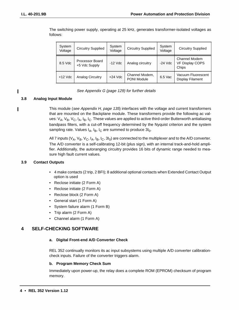
The switching power supply, operating at 25 kHz, generates transformer-isolated voltages asfollows:
See Appendix G (page 129) for further details
3.8 Analog Input Module
This module (see Appendix H, page 135) interfaces with the voltage and current transformersthat are mounted on the Backplane module. These transformers provide the following ac val-ues: VA, VB, VC, IA, IB, IC. These values are applied to active third-order Butterworth antialiasing
bandpass filters, with a cut-off frequency determined by the Nyquist criterion and the systemsampling rate. Values IA, IB, IC are summed to produce 3I0.
All 7 inputs (VA, VB, VC, IA, IB, IC, 3I0) are connected to the multiplexer and to the A/D converter.
The A/D converter is a self-calibrating 12-bit (plus sign), with an internal track-and-hold ampli-fier. Additionally, the autoranging circuitry provides 16 bits of dynamic range needed to mea-sure high fault current values.
3.9 Contact Outputs
• 4 make contacts (2 trip, 2 BFI); 8 additional optional contacts when Extended Contact Outputoption is used
• Reclose initiate (2 Form A)
• Reclose initiate (2 Form A)
• Reclose block (2 Form A)
• General start (1 Form A)
• System failure alarm (1 Form B)
• Trip alarm (2 Form A)
• Channel alarm (1 Form A)
4 SELF-CHECKING SOFTWARE
a. Digital Front-end A/D Converter Check
REL 352 continually monitors its ac input subsystems using multiple A/D converter calibration-check inputs. Failure of the converter triggers alarm.
b. Program Memory Check Sum
Immediately upon power-up, the relay does a complete ROM (EPROM) checksum of programmemory.
SystemVoltage
Circuitry SuppliedSystemVoltage
Circuitry SuppliedSystemVoltage
Circuitry Supplied
8.5 VdcProcessor Board+5 Vdc Supply
-12 Vdc Analog circuitry -24 VdcChannel ModemVF Display COPSChips
+12 Vdc Analog Circuitry +24 VdcChannel Modem,PONI Module
6.5 VacVacuum FluorescentDisplay Filament
Power Automation and Protection Division
REL 352 Version 1.12 • 5
1c. Power Up RAM Check
Immediately upon power-up, the relay does complete RAM memory read/write tests.
d. Nonvolatile RAM Check
All settings and targets are stored in nonvolatile RAM in three identical arrays. These arrays arecontinuously checked by the program. If all three array copies disagree, a nonvolatile RAM fail-ure is detected.
5 UNIQUE REMOTE COMMUNICATION (WRELCOM) PROGRAM
Two optional types of remote interface can be ordered.
• RS232C for single point computer communication.• INCOM for local network communication.
A special PC software (WRELCOM RCP and OSCAR) program are available for obtaining orsending the setting information to the REL 352. The REL 352 front panel shows two faultevents (last and previous faults), but with the remote communication, 16 fault events and 3records of oscillographic data can be obtained and stored. Each record of the oscillographicdata contains 8-cycle information (1-prefault and 7-post-fault), with 7 analog inputs and 24 dig-ital data (at the sampling rate of 12 per cycle).
I.L. 40-201.9BP
ower A
utomation and P
rotection Division
6•
RE
L 352 Version 1.12
PONI BACKPLANE BD.
PROCESSOR BD.
DISPLAY BD.
FT
-14
PO
WE
R S
UP
PLY
AN
ALO
GIN
PU
T B
D.
FT
-14
OPTOISOLATED INPUT BD. RELAY OUTPUT BDS.
XFMR
INTERCONNECT BD.
SPT
Top View
Figure 1-1: Layout of REL 352 Modules within Inner and Outer Chassis

Pow
er Autom
ation and Protection D
ivision
RE
L 352 Version 1.12
•7
1
Sub 991618C33ØA
TripDirection
Line
ctIAR
IA6
5
Figure 1-2: Block Diagram of REL 352 Relay

I.L. 40-201.9B Power Automation and Protection Division
8 • REL 352 Version 1.12
THIS PAGE RESERVED FOR NOTES

Power Automation and Protection Division
REL 352 Version 1.12 • 9
2
Section 2. REL 352 SPECIFICATIONS
1 TECHNICAL
1.1 Principle of Operation
Phase Comparison, Single-Comparer and Dual Comparer using Low Speed Power LineCarrier (ON-OFF and FSK), Audio Tone and Microwave.
1.2 Miscellaneous
Nominal ac Voltage (VLN) at 60 Hz 69.3 V rms
Nominal ac Current (In) 1 or 5 A rms
Rated Frequency 50 or 60 Hz
Maximum Permissible ac Voltage:
• Continuous 160 V rms— (limited by maximum input to A/D converter)
• 10 Second 240 V rms— (limited by input transformer flux density)
Maximum Permissible ac Current:
• Continuous 15 A rms— (limited by thermal characteristics)
• 1 Second
Operational 160 A rms - 5 A nominal32 A rms - 1 A nominal— (limited by maximum input
to the A/D converter)
Thermal 500 A
dc Battery Voltages:
Nominal Input Range
60/48 Vdc 38 - 70 Vdc110/125 Vdc 88 - 145 Vdc
110/125 Vdc 88 - 150 Vdc
220/250 Vdc 176 - 280 Vdc
dc Burdens:
Battery 15 W normal40 W tripping
ac Burdens:
Volts per Phase 0.02 VA at 70 Vac
Current per Phase 0.45 VA at 5 A
2 EXTERNAL CONNECTIONS
Terminal blocks located on the rear of the chassis suitable for #14 square tongue lugs.
Wiring to FT-14 switches suitable for #12 wire lugs.
I.L. 40-201.9B Power Automation and Protection Division
10• REL 352 Version 1.12
3 CONTACT DATA
Trip Contacts — make & carry 30 A for 1 second, 10 A continuous capability, break 50 wattsresistive or 25 watts with L/R = .045 seconds.• Non-Trip Contacts
1 A Continuous0.1 A Resistive Interrupt Capability
Contacts also meet IEC - 255-6A, IEC - 255-12, IEC -255-16, BS142-1982.
4 COMMUNICATION EQUIPMENT INTERFACE
4.1 INPUTSOptoisolated (7500 V peak) jumper configurable for 20 V, 48 V, 125 V external dc Power SupplyOperation “On” State Current:
20 V 15 mA48 V 6 mA125 V 6 mA
Interfaces to Power Line Carrier (ON-OFF and FSK) Audio Tone and Microwave.
Mark 1 Not used with ON/OFF carrier schemesSpace 1Channel Failure 1Mark 2Space 2Channel Failure 2
4.2 OUTPUTOptoisolated (7500 V peak) Power Transistor Output (Rated 400 V) supporting external dcpower supply operation in the range of 20 - 150 V dc.
Interfaces to:
Carrier on/off (for ON-OFF PLC) or Carrier mark / space (for FSK PLC) control.
5 OPTIONAL COMPUTER/NETWORK INTERFACE
• RS232C/PONI — for single point computer communications• INCOM/PONI — for local network communications using INCOM network
6 CHASSIS DIMENSIONS AND WEIGHT
Height 7" (177.8 mm) 4 Rack Units (See figure 2-1, page 12)
Width 19" (482.6 mm)
Depth 14" (356 mm) including terminal blocks
Weight 38 lb. (17.5 kg)
3 Terminal Applications Used only on
Power Automation and Protection Division
REL 352 Version 1.12 •11
27 ENVIRONMENTAL DATA
Ambient Temperature Range
• For Operation — 20°C to +60°C• For Storage — 40°C to +80°CInsulation Test Voltage 2.8 kV, dc, 1 minute (3.2 kV dc, 1 sec) ANSI, C37.90 IEC-255-5
Open contacts 1400 Vdc continuous
Impulse Voltage Withstand 5 kV Peak, 1.2/50 microseconds, 0.5 Joule, (IEC-225-5)
Surge Withstand Voltage 3 kV, 1 MHz (ANSI C37.90.1, IEC-255-22-1)
Fast Transient Voltage 4 kV, 10/100 ns Withstand (ANSI C37.90.1, IEC 255-22-4)
EMI Field Strength Withstand 25 MHz-1GHz, 10V/m Withstand (ANSI C37.90.2)
Electrostatic Discharge Tests (IEC 255-22-2, IEC, 801-Y) 8/12 kV test voltage.
Emission Tests (EN 55022, Class A)

I.L. 40-201.9BP
ower A
utomation and P
rotection Division
12•
RE
L 352 Version 1.12
Figure 2-1: REL 352 Outline Drawing
(447.294)17.610 (21.666)
0.853
(346.049)13.624
(290.601)11.441
(17.653)0.695
(482.600)19.000
0.242(6.147)
0.090(2.286)
1.477(37.516)
.140 R(3.556)
4.000(101.600)
6.954(176.632)
Power Automation and Protection Division
REL 352 Version 1.12 •13
3
1 INTRODUCTION
The REL 352 is a dual-microprocessor based, composite sequence filter, phase comparisonprotection system. The REL 352 operates on the principles inherited from previous successfulphase comparison relaying systems; but, adapted and improved using numerical techniques.
The REL 352 is a communication channel dependent system optimized for operating with pow-er line carrier equipment. Either ON-OFF or FSK (frequency shift) power line carrier equipmentcan be used to interface with the REL 352.
It may also interface to other communication equipment that accepts a low frequency (60/50Hz) modulation such as Single-Side-Band (SSB) PLC, Audio Tone or analog microwave.
The REL 352 is a high speed relaying system; suitable for application to any voltage level. Itsprinciple of operation makes it ideal for short lines and tapped lines with a power transformer,where traditional distance protection fails.
An optional distance-type relaying system has been included to provide back-up for a loss ofcommunication channel. This back-up system is similar to a zone 2 and zone 3 distance unitsand logic for a distance non-pilot relaying system. Phase and ground distance units are includ-ed.
The phase comparison protection is inherently immune to systems’ swings and the relay willnot trip. However if trip is desired the optional distance relaying system has blinders for detect-ing this condition. OST (Out-of-Step Trip) is included. Trip under OST conditions may be se-lected via a relay setting.
An Overcurrent tripping function is also included in the relaying system. The “Highset” overcur-rent function activates the trip outputs when the phase (IPH) or the ground (IGH) threshold unitsdetect currents above the settings. These units may be supervised (it is recommended that theybe supervised) by the directional units. The phase units are supervised by FDOP and theground unit is supervised by FDOG. Of course the connection of external voltage transformersto REL 352 is required to activate directional units.
The REL 352 also requires the connection to Voltage Transformers (vt’s) for distance protec-tion, fault location, loss of potential and loss of current detection.
Because of the settings ranges available in the relaying system, it is possible to accommodatedifferent ct ratios at the terminals of the transmission line.
The REL 352 has the capability of communication channel propagation delay measurement,which is very important for the correct operation of the relaying system. Once this delay hasbeen measured, it will be entered as a system setting. It is assumed that the channel delay inthe communication equipment will remain constant for the life of the transmission line andphase comparison relaying system. If so desired, periodic tests of the propagation delay canbe easily performed.
Section 3. APPLICATIONS AND ORDERING INFORMATION
I.L. 40-201.9B Power Automation and Protection Division
14 • REL 352 Version 1.12
2 COMPOSITE SEQUENCE FILTER PHASE COMPARISON
Current only systems, like the REL 352, compare the currents measured at the terminals of thetransmission line. In a phase comparison system, like the REL 352, the phase relationship de-termines whether the condition is internal or external.
For an internal fault, the currents are essentially “in phase” at the terminals of the transmissionline. For an external fault; the currents are 180˚ out of phase. Figure 3-1(page 22), illustratesthe concept.
The REL 352 combines the phase current (IA, IB and IC) measured at the protective relayingterminal into a single quantity. This quantity is an output of Symmetrical Component Filter whichis proportional to the weighted sum of the sequence components. Figure 3-2 (page 23), illus-trates this filter.
The quantity IT, therefore, is defined as:
(3.1)
The Positive, Negative, and Zero sequence quantities are calculated from the sampled currentdata as follows:
Per Clark’s components:
The quantity IT is itself is normally a sine wave. The C1 (positive sequence weighting coeffi-cient), C2 (negative sequence weighting coefficient) and C0 (zero sequence weighting coeffi-cient) are system settings that control the sensitivity of the relaying system. For dynamic rangeconsiderations, the sequence filter has a saturation characteristic whereby the signal clamps at
± 160 amps on a 5 amp rated ct system or ± 32 amps maximum on a 1 amp rated ct
system.
IT C0I 0 C– 1I 1 C2I 2+=
I αm
2 I Am IBm– ICm–×( )3
--------------------------------------------------------=
Iβm
IBm ICm–( ) 3×3
--------------------------------------------=
Iposm I 1m
I αm I α
m 1–+( )4
-----------------------------------3 (I βm I βm 1– )–×
π--------------------------------------------+= =
Inegm I 2m
I αm I α
m 1–+( )4
-----------------------------------3 (I βm I βm 1– )–×
π--------------------------------------------–= =
Izerom I 0m
I Am IBm ICm+ +( )3
------------------------------------------------= =
Icompm ITm I 1m C1) (I 2m C2) (I 0m C0×+×+×–( )= =
2 2

Power Automation and Protection Division
REL 352 Version 1.12 •15
32.1 Local Positive (LP) and Local Negative (LN)
LP & LN waveforms are used to represent a phase of positive and negative half-cycle of the ITsignal at a local terminal.
The local positive LP is defined as a logic “1” in the positive region of IT above the thresholdLP; otherwise it is a “0”.
The local negative LN is defined as a logic “1” in the negative region of IT below the thresholdLN; which is = - LP setting, otherwise it is a “0”.
2.2 IKEY
The IKEY level is provided to define the threshold generating the squarewave to be sent to theremote terminal. The IKEY level is defined in the positive region. Above the threshold level, de-termined by the IKEY setting local terminal will “key” a logic “1” to the remote terminal via theIKEY output signal.
3 FSK POWER LINE CARRIER AND AUDIO TONE APPLICATIONS
Internal Fault
The signals generated during an internal fault are shown in figure 3-4 (page 24). Note that thelocal and remote currents are essentially in phase. The local terminal generates the LP and LNsignals based on the local IT quantity.
The IKEY signal is generated in the remote terminal and transmitted over the communicationschannel (for example, power line carrier) and received in the local terminal as MARK andSPACE signals subjected to communication propagation delay (CPD).
The local terminal provides compensation for CPD by delaying local quantities LP and LN usingsettings LDT1 and LDT2 (for 3-terminal applications).
The MARK signal and the LP signal are ANDed and a “positive trip coincidence” condition isgenerated. The same is true with the SPACE and LN signals. The two are ANDed together anda “negative trip coincidence” condition is asserted. The composite COIN signal is generated. ACOIN signal of at least 4 msec need for a trip.
External Fault and Load Condition
For an external fault (and load condition), the signal relationship is shown in figure 3-5 (page25). Due to the current directions at both ends, the currents into the relaying units in the localand remote sites will be 180˚ out of phase. When ANDing the MARK and LP and the SPACEand LN signals, the outputs of the “positive trip coincidence” and “negative trip coincidence”conditions will be zero all the time. Therefore, the COIN output will be constant logic “0”.
4 ON-OFF POWER LINE CARRIER APPLICATIONS
As seen on figures 3-6 and 3-7 with ON/OFF PLC communications (COMM setting = 2), phasecomparisons are performed only on the negative half-cycle of the power waveforms in a block-ing type scheme. Tripping can only occur during half-cycles of time in which neither end is key-ing which occurs only when both terminal’s IT currents are sufficiently “in-phase”, and are thuskeying “in-phase”.
I.L. 40-201.9B Power Automation and Protection Division
16 • REL 352 Version 1.12
The ON/OFF PLC’s receiver detector outputs must be connected to the SPACE1/(Trip Nega-tive) and SPACE2/(Trip Negative) inputs of the REL 352 relay system. Normally the SPACE/(Trip Negative) input(s) as seen by the microprocessor should be a solid “1” state when the re-mote transmitter is in the quiescent or unkeyed state. This is typically achieved by the polarityinversion which naturally occurs in the relay’s optocoupler input stages. Thus the polarity jump-ers JMP5 and JMP3 on the interconnect module for the SPACE1/(Trip Negative) and SPACE2/(Trip Negative) inputs should both be set for “Normal” operation. This corresponds to JMP po-sition 2-3 for both jumpers. For more information on polarity considerations, see Appendix K,Section 2.
Internal Fault
For internal faults the SPACE and LN signals produce positive coincidence COIN as shown onfigure 3-6 (page 26).
External Fault
The external fault is illustrated in figure 3-7 (page 27). The LN and SPACE comparison resultsin no coincidence (“0” state) and a pilot trip is blocked.
5 THREE TERMINAL APPLICATIONS
If a FSK system is used for a three terminal application, there will be two sets of MARK andSPACE signals received from the remote locations. The M1 and S1 (from remote terminal 1)and M2 and S2 (from remote terminal 2) are compared to the respective LP1, LN1, LP2 andLN2 signals delayed by the respective LDT1 or LDT2 settings. It is extremely important that thesettings reflect the true channel delays of the communications channel. The correct comparisonof phases is totally dependent on the proper channel delay measurement.
If an ON/OFF carrier system is used for a three terminal application, the relay should be set to2 TERM. As the ON/OFF carrier system is a blocking scheme all three terminals operate overthe same channel.
6 PILOT TRIP LOGIC
The system logic diagram illustrates the decision logic for the REL 352. The comparison signal,COUT feeds into a 4 millisecond timer (supervised by FD1 and FD2, fault detector signals ex-plained later). For security purposes, to account for inaccuracies and transmission line chargingcurrent effects, a minimum width of the squarewave logic “1” level is required. This is accom-plished through a pick-up timer of 4 milliseconds.
If the setting in the logic indicates a ONE count requirement (CNT = 1) it implies that a COUT sig-nal that generates a pulse of at least 4 milliseconds will indicate a trip condition and PLT = “1”.
If the setting CNT = 2 indicating a TWO count requirement, more security is introduced in thetrip decision. For this setting, COUT should produce two logic “1” pulses of at least 4 millisec-onds within a 25 millisecond period (for FSK PLC) or 40 msec (for ON-OFF PLC) to assert thepilot trip PLT = “1”. In the event that the first pulse is greater than 6 milliseconds, indicating arobust fault, a bypass timer produces the trip on the first count. Security is improved if the twocount setting is used.
The trip (PLT) signal is enabled as long as FD1 and FD2 are active.
Power Automation and Protection Division
REL 352 Version 1.12 •17
3The FD1 and FD2 units are fault detectors that are measuring the output of the sequence filter,IT. Both FD1 and FD2 can be set to operate on current level (ITA1 and ITA2) only, currentchange detectors (DIT1 and DIT2) only, or current level and change detector in an OR or ANDlogic. The output from the FD2 fault detector can be set with or without 150 msec drop-out de-lay. It is recommended to use the dropout delay setting when current change detector DIT2 isused for the FD2 signal.
In addition, the system provides another fault detector, CD, that measures the change in thecurrent (and voltage) quantities. CD operates in parallel with DIT1 and is also used for super-vision of the unblock logic. If external voltage transformers are connected to REL352, it is ad-visable to include the voltage change detectors (CD=∆V∆I).
7 DIRECTIONAL OVERCURRENT UNITS
Phase and ground directional units (FDOP and FDOG) may be set either in or out. When theyare in, the high-set overcurrent units (IAH, IBH, ICH and IGH) are directional. The ground direc-
tional unit may either be zero sequence polarized or negative sequence polarized.
Zero sequence polarization utilizes the zero sequence components of the currents and voltag-es into the relay, and the unit operates when 3Io leads 3V0 by more than 30° or lags by more
than 150°. For the operation of these units, it is required that 3I0 > 0.5 amp and 3V0 > 1 Volt.
Negative sequence polarization utilizes the negative sequence components of the currents andvoltages into the relay and the unit has its maximum torque line when the current 3I2 > 0.5 amp
and 3V2 > 3 Volts.
FDOG may be used for detecting high ground resistance faults that may not be detected by anyof the ground distance units. TOG may be blocked or given a definite time for operation onceFDOG has operated and IoM has picked up.
The phase directional unit (FDOP) is based on the angular relationship of a single-phase cur-rent and the corresponding pre-fault phase-to-phase voltage phasors. The forward direction isidentified if the current phasor leads the voltage phasor. The pair of current and voltage phasorswhich are compared are IA and VBA (FDOPA), IB and VCB (FDOPB), IC and VAC (FDOPC). The
three-phase fault detection of Zone 2 and 3t are supervised by FDOPA and FDOPB andFDOPC. The high set currents IAH, IBH, ICH are supervised by FDOPA, FDOPB and FDOPC,
respectively.
The logic for this unit is shown in figure 3-17 (page 33).
8 OPTIONAL BACK-UP
8.1 Distance Relaying
The Distance units in the REL 352 relay system are only operative when the communicationschannel is unsound. The back-up distance relaying system only includes Zone 2 and Zone 3 ofa conventional non-pilot distance relaying system.
Line measurement techniques applied to each zone include:
• Single phase-to-ground fault detection
• 3-Phase fault detection
I.L. 40-201.9B Power Automation and Protection Division
18 • REL 352 Version 1.12
• Phase-to-phase fault detection
• Phase-to-phase-to-ground fault detection
8.2 Single Phase-to-Ground
Single phase-to-ground fault detection (see figure 3-12, page 28) is accomplished by 3 non-directional phase units (A, B, C). Expressions 1 and 2 (below) are for the operating and refer-ence quantity, respectively. The unit will produce output when the operating quantity leads thereference quantity.
eq. (1)
and
eq. (2)
where
VXG = VAG, VBG or VCG
IX = IA, IB or IC
I0 = zero sequence relay current
Z1L, Z0L = Positive and zero sequence line impedance in relay ohms
ZFG = Forward zone reach setting in secondary ohms for SLGF
ZRG = Reverse reach setting in secondary ohms for SLGF
8.3 Three-phase
Three-phase fault detection (see figure 3-13, page 29) is accomplished by the logic operationof one of the three ground units, plus the 3øF output signal from the phase selector unit.
However, for a 3-phase fault condition, the computation of the distance units will be:
VXG - IXZP eq. (3)
and VQ eq. (4)
Where VQ = Quadrature Phase Voltages, i.e.
VCB,VAC, and VBA for phase A, B and C unit, respectively
VXG = VAG, VBG, VCG
IX = IA, IB or IC
ZP = Zone reach settings (Z2P, Z3P) in secondary ohms
VXG I X
Z0L Z1L–
Z1L--------------------------- I 0+ ZFG–
j V XG I X
ZOL Z1L–
ZL---------------------------- I 0+
ZRG+
13--- I A I B I C+ +( )
Power Automation and Protection Division
REL 352 Version 1.12 •19
38.4 Phase-to-Phase
The Phase-to-Phase unit (see figure 3-14, page 30) responds to all forward Phase-to-Phasefaults, and some phase-phase-to-ground faults. Expressions 5 and 6 are for operating and ref-erence quantity, respectively. They will produce output when the operating quantity leads thereference quantity.
(VAB - IABZP) eq. (5)
(VCB - ICBZP) eq. (6)
NOTE: Phase-to-phase-to-ground faults will be detected by the operation of eithertwo-phase-to-ground or phase-to-phase units with 3I 0 > I0m
8.5 Zone 2 and Zone 3 Distance Relaying
The optional back-up system in REL 352 consists of two zones of distance protection for bothphase and ground faults.
Each zone consists of four distance units that are able to detect all fault types. The impedanceunits are three-phase-to- Ground units (ag, bg and cg) and a Phase-to-Phase unit.
The phase-to-ground units detect all Single Line-to- Ground Faults (SLGF), three-phase faultsand some phase-to-phase-to-ground faults within its operating characteristic. The ZGF andZGR (forward and reverse) settings apply to ground faults and the ZP settings apply to 3 Phase
faults.
The phase-to-phase unit detects all phase-to-phase faults and some phase-to-phase-to-groundfaults. Since this unit is inherently directional only the forward reach is used. ZP (forward phasesetting) applies to phase-to-phase faults.
NOTE: All phase-to-phase-to-ground faults are covered by the operation of the de-scribed units.
For the indication of a phase distance trip the following conditions have to occur:
1. For a three-phase fault, the RT blinder (if the system has OST logic included) and no OSBand the 3Ph output of the phase selector have to have operated to indicate a three-phasefault.
2. For a Phase-to-Phase fault only the Phase-to-Phase unit needs to operate to indicate aPhase-to-Phase fault.
3. For a phase-to-phase-to-ground fault either the phase-to-phase unit or the phase-to-ground units have to operate to indicate a phase-to-phase-to-ground fault.
4. For a single line to ground fault, any of the phase-to-ground fault units have to operate toindicate a phase-to-ground fault.
The phase fault detection is supervised by IL, the low set overcurrent unit.
The phase-to-ground fault detection is supervised by I0m.
Each zone has its own timer to time coordinate with relays further away for step distance relay-ing. Separate phase and ground timers are provided.
The impedance back-up logic is shown in figure 3-16 (page 32).
I.L. 40-201.9B Power Automation and Protection Division
20 • REL 352 Version 1.12
9 MISCELLANEOUS FUNCTIONS
9.1 Out-of-Step Trip (OST) and Out-of-Step Block (OSB) Logic
Out of step detection in REL 352 is achieved by the use of blinders. Only units with optionalback-up have this logic since for the blinder implementation voltage inputs are required.
A two blinder scheme is used for detecting Out-of-Step conditions. The two blinders are called21 BO (Outer Blinder) and 21 BI (Inner Blinder) and are parallel to the line impedance setting,i.e., they are tilted by the PANG setting.
The RU and RT settings are the distance perpendicular to the line impedance that the blindersare displaced from the latter. This is illustrated in figure 3-18 (page 34). The RT setting is alsofor load restriction and if any three-phase fault occurs, the inner blinder, 21 BI has to be acti-vated for tripping and the impedance be in either Zone 2 or Zone 3 reach.
Figure 3-19 shows the OST and OSB logic.
The duration of time it takes 21 BI to operate after 21 BO operates is the indication of an Outof Step condition. Timer OST1 controls this time. When the timer times out, an Out of Step con-dition has been detected. An OSB signal is immediately sent to block the operation of Zone 2and Zone 3 distance units.
Timer OST2 times the trip after an OST condition has been detected and the trajectory movesfrom point 2 to point 3 in figure 3-18 (page 34). When OST 2 times out a trip signal is sent if theREL 352 has been set to trip on the way in under out of step conditions.
Timer OST3 starts timing after the inner blinder operates. If the timer has timed out then trippingwill be allowed immediately (with a 20 millisecond time delay) once the outer blinder (21 BO)resets. Otherwise, OST has to time out first. OST3 controls the trip for an OST condition on theway out, as illustrated by the points 4 and 5 in figure 3-18 (page 34).
The OSOT timer is an Out of Step over-ride Timer that bypasses OSB after it has timed out andlets the relay trip.
9.2 Loss of Potential (LOPB)
This logic is implemented in the relay when the optional back-up distance protection is included.Loss-of-Potential Block (LOPB) is used to supervise the distance measurements in the backupsystem. When this condition exists, all impedance measuring units will have their outputsblocked.
The simple logic is shown in figure 3-15 (page 31). This logic will detect one or two blown fuses,but will fail to detect the unlikely failure of all three-phase fuses. The output of this logic will alsoenergize the failure alarm relay.
9.3 Loss of Current (LOI)
This logic is provided when the backup system is included in the relaying system.
The simple logic (shown in figure 3-15) will detect the loss of one or two current inputs. Theoutput of this logic is only used to energize the failure alarm relay of REL 352.
Power Automation and Protection Division
REL 352 Version 1.12 •21
310 RECLOSING LOGIC
REL 352 provides 3-phase Reclose Initiate contact outputs to be used with an external reclos-ing relay. A Reclose Block (RB) contact output is also provided. The relaying system will blockthe reclosing relay if reclosing into a permanent fault.
The Reclose Block Enable (RBEN) setting has the following options:
• NORB - No reclosing block• ALRB - Reclose block for all fault types
With 52b contact open (closed breaker) the sequence of operation is:fault applied >> Pilot Trip >> Reclose initiate.
With 52b closed (open breaker) the sequence becomes:52b closed >> fault applied >> Pilot Trip >> RIFT >> Reclose block.
Explanation:Closing of 52b before applying fault enables the RIFT logic after 250 msec. The Pilot Trip ap-pears to the relay to be on a first reclose rather than on initial trip, the RIFT prevents a “second”reclose.
Initial trip is always without 52b (breaker closed), thus a reclose is initiated. When the breakeropens on the initial trip, 52b closes and RIFT is armed in 250 msec.
When the breaker is closed on the first reclose 52b opens, but is held “on” logically for 500msec to the RIFT logic.
A Pilot Trip within that 500 msec is interpreted as having reclosed onto the same fault, and fur-ther reclosing is blocked.
11 FAULT LOCATOR
The REL 352 fault locator feature computes the magnitude and phase angle of the fault imped-ance and the distance to the fault in both miles and kilometers. The fault impedance is calcu-lated from the voltage and current phasors of the faulted phase(s). Thus, proper faulted phaseselection is essential for good fault locator results. The distance to the fault is computed by mul-tiplying the imaginary part of the fault impedance times (VTR/CTR), the voltage transformerand current transformer ratios, and dividing by the distance multiplier setting (XPUD). The im-pedance calculations for the various fault types are:
ZXG = VXG / (IX + KI0)
for single line to ground faults,
ZXY = (VXG - VYG) / (IX - IY)
for line to line faults, and
ZABC = VA / IA
for three-phase faults.
(X, Y = Any A, B, C phase)
This function is included in REL 352 when the optional distance back-up system is included.

I.L. 40-201.9BP
ower A
utomation and P
rotection Division
22•
RE
L 352 Version 1.12
1) “Normal Internal Fault”
2) “External Fault”
Figure 3-1: REL 352 Phase Comparison, Fault Recognition
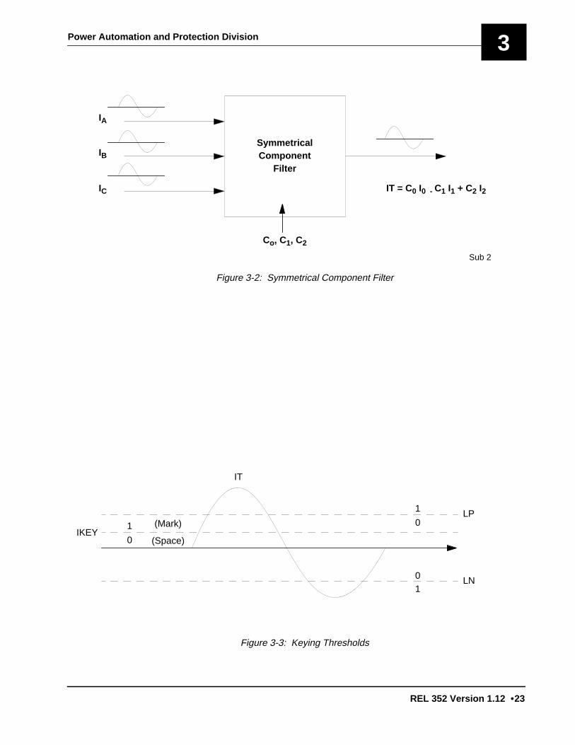
Power Automation and Protection Division
REL 352 Version 1.12 •23
3
SymmetricalComponent
Filter
IA
IB
IC IT = C0 I0 - C1 I1 + C2 I2
1
0
0
1
10
LP
LN
(Mark)
(Space)IKEY
IT
Co, C1, C2
Sub 2
Figure 3-2: Symmetrical Component Filter
Figure 3-3: Keying Thresholds
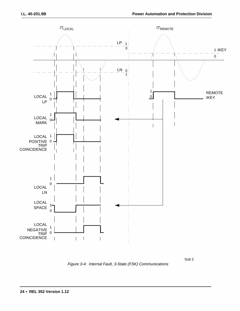
I.L. 40-201.9B Power Automation and Protection Division
24 • REL 352 Version 1.12
01
10
LP
LN
ITLOCAL
1
0
IKEY
ITREMOTE
IKEYLP
LN
MARK
SPACE
POSITIVE
NEGATIVE
1
01
0
1
0
1
0
1
0
1
0
TRIPCOINCIDENCE
TRIPCOINCIDENCE
Sub 2Figure 3-4: Internal Fault, 3-State (FSK) Communications
REMOTE
LOCAL
LOCAL
LOCAL
LOCAL
LOCAL
LOCAL
1
0
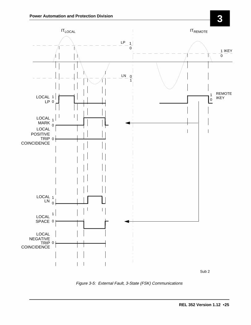
Power Automation and Protection Division
REL 352 Version 1.12 •25
3
01
10
LP
LN
ITLOCAL
IKEY
ITREMOTE
LP
LN
MARK
TRIP
SPACE
TRIP
POSITIVE
NEGATIVE
01
01
01
0
1
0
0
0
1
IKEY
01
COINCIDENCE
COINCIDENCE
Sub 2
Figure 3-5: External Fault, 3-State (FSK) Communications
REMOTELOCAL
LOCAL
LOCAL
LOCAL
LOCAL
LOCAL
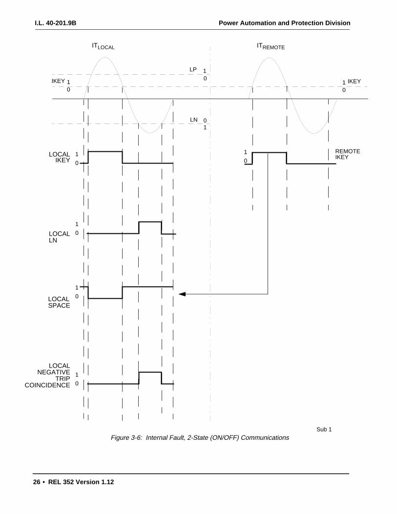
I.L. 40-201.9B Power Automation and Protection Division
26 • REL 352 Version 1.12
01
10
LP
LN
ITLOCAL
IKEY
ITREMOTE
LOCAL
LOCAL
TRIPNEGATIVE
0
10
1 REMOTE
01
COINCIDENCE
Sub 1
IKEYIKEY
LN0
1
0
1
LOCALSPACE
0
1
Figure 3-6: Internal Fault, 2-State (ON/OFF) Communications
LOCAL
IKEY
01
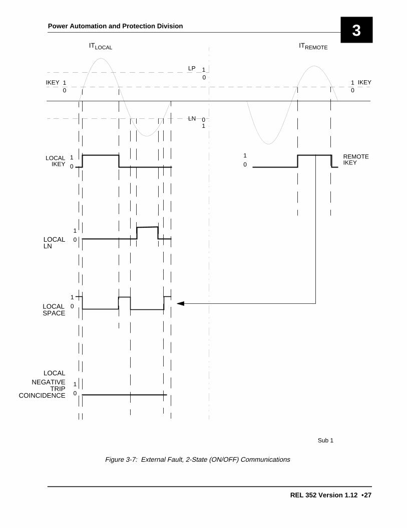
Power Automation and Protection Division
REL 352 Version 1.12 •27
3
01
10
LP
LN
ITLOCAL
IKEY
ITREMOTE
LOCAL
LOCAL
TRIPNEGATIVE
0
10
1 REMOTE
01
COINCIDENCE
Sub 1
IKEYIKEY
LN0
1
0
1
LOCALSPACE
0
1
Figure 3-7: External Fault, 2-State (ON/OFF) Communications
IKEY01
LOCAL

I.L. 40-201.9B Power Automation and Protection Division
28 • REL 352 Version 1.12
Figure 3-8: Mho Characteristics for Single Phase-to-Ground Fault Detection
ESK00042Sub 6
FDOG: Forward Directional/Overcurrent Ground Unit
ZGF: Forward Reach Setting
ZGR: Reverse Reach Setting
ϒ: Maximum Torque Angle
B: Balance Point
α: 30˚ w/DIRU set to ZSEQ
α: 8˚ w/DIRU set to NSEQ
R
ZGR
ZGF
ϒ
B
FDOG
j
α
X
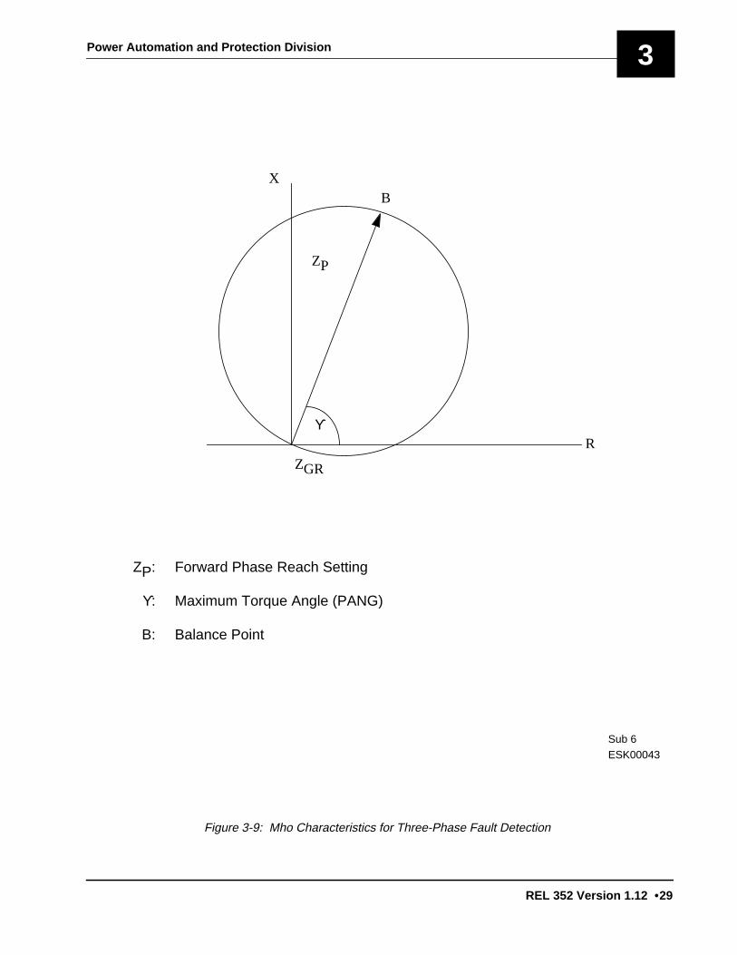
Power Automation and Protection Division
REL 352 Version 1.12 •29
3
Figure 3-9: Mho Characteristics for Three-Phase Fault Detection
X
ZP
ZGR
R
ZP: Forward Phase Reach Setting
ϒ: Maximum Torque Angle (PANG)
B: Balance Point
ϒ
B
ESK00043Sub 6
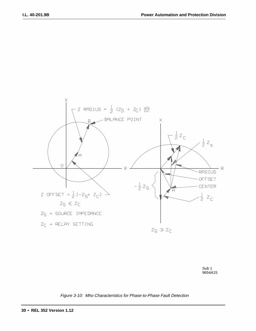
I.L. 40-201.9B Power Automation and Protection Division
30 • REL 352 Version 1.12
Figure 3-10: Mho Characteristics for Phase-to-Phase Fault Detection
Sub 19654A15
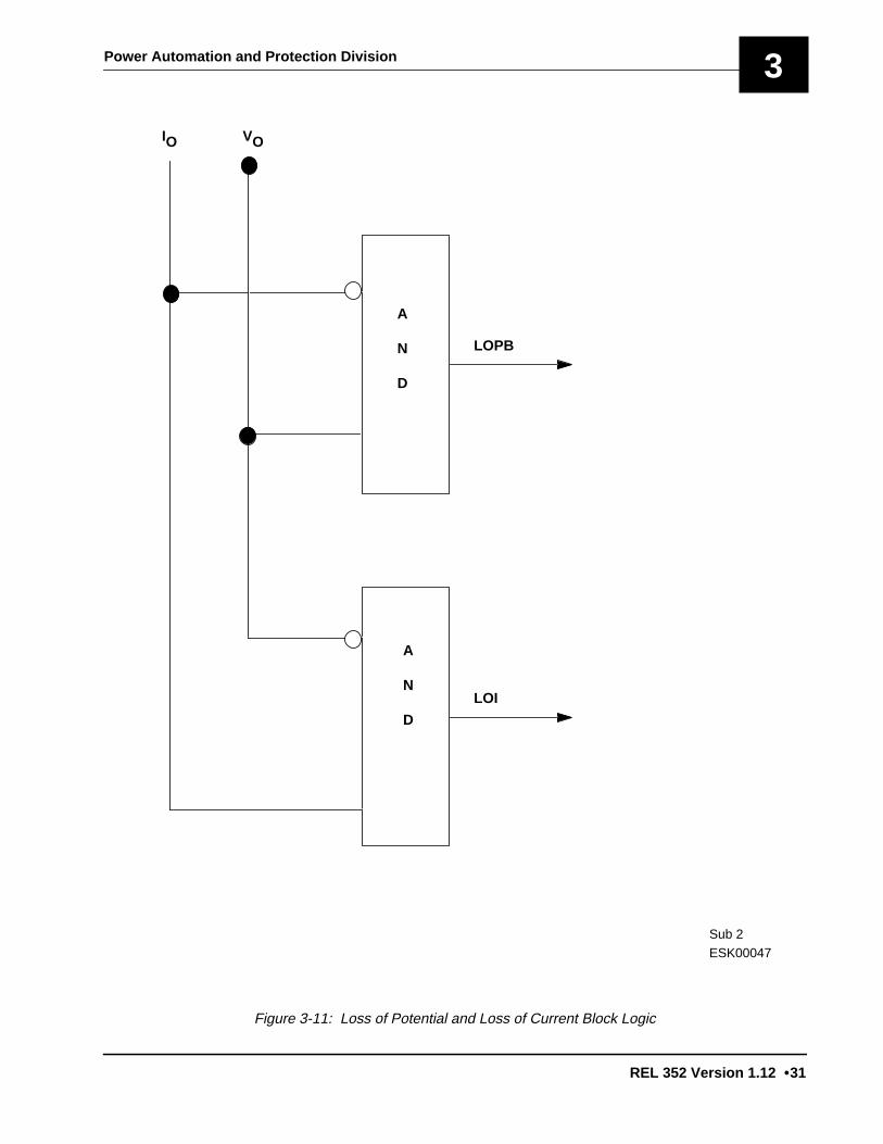
Power Automation and Protection Division
REL 352 Version 1.12 •31
3
Figure 3-11: Loss of Potential and Loss of Current Block Logic
IO VO
A
N
D
A
N
D
LOPB
LOI
ESK00047Sub 2
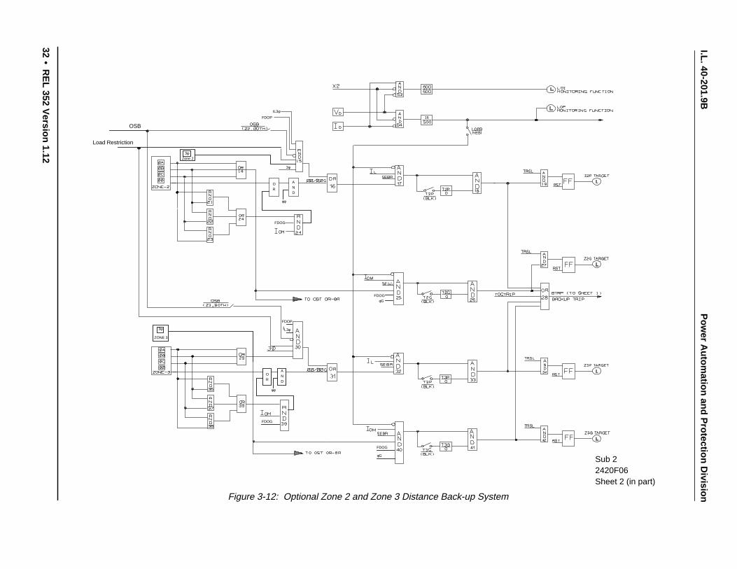
I.L. 40-201.9BP
ower A
utomation and P
rotection Division
32•
RE
L 352 Version 1.12
Figure 3-12: Optional Zone 2 and Zone 3 Distance Back-up System
Sub 22420F06Sheet 2 (in part)
FDOP
IL3φ
3φZone 2
3φ
FDOG
φφ
AND
OR
FDOGφG
FDOG
OR
AND
φφ
ZONE 3
3φ
FDOG
φG
16
FDOP
IL3φ
Load Restriction
OSB
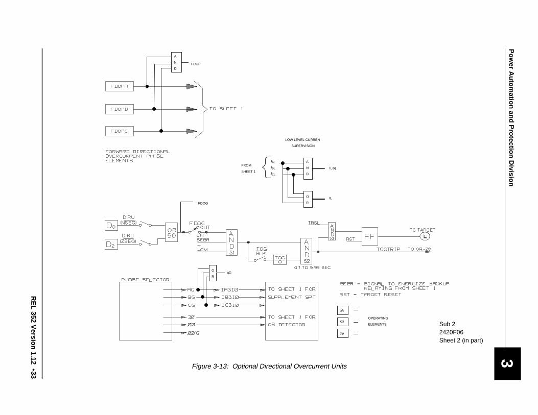
Pow
er Autom
ation and Protection D
ivision
RE
L 352 Version 1.12
•33
3
Figure 3-13: Optional Directional Overcurrent Units
A
N
DFDOP
FDOG
φG
φA
φφ
3φ
OPERATING
ELEMENTS
A
N
D
O
R
IL3φ
IL
LOW LEVEL CURREN
SUPERVISION
FROM
SHEET 1
IAL
IBL
ICL
Sub 22420F06Sheet 2 (in part)
O
R
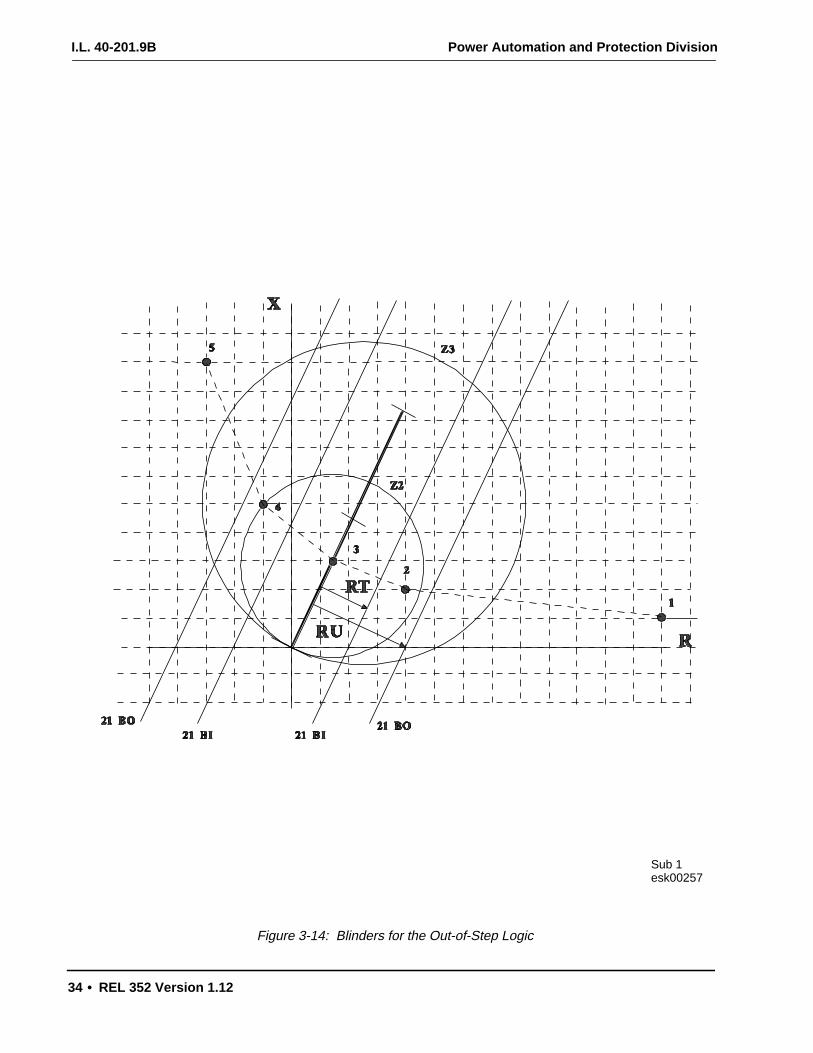
I.L. 40-201.9B Power Automation and Protection Division
34 • REL 352 Version 1.12
Figure 3-14: Blinders for the Out-of-Step Logic
Sub 1esk00257

Pow
er Autom
ation and Protection D
ivision
RE
L 352 Version 1.12
•35
3Figure 3-15: Optional OST and OSB Logic Diagram
* Denotes Change
Sub 22420F06Sheet 2 (in part)
φ
φ
φ
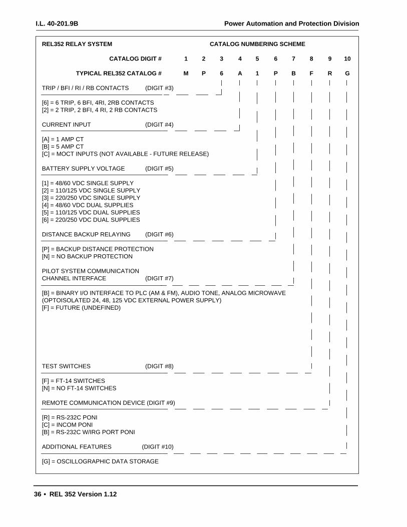
I.L. 40-201.9B Power Automation and Protection Division
36 • REL 352 Version 1.12
REL352 RELAY SYSTEM CATALOG NUMBERING SCHEME
CATALOG DIGIT # 1 2 3 4 5 6 7 8 9 10
TYPICAL REL352 CATALOG # M P 6 A 1 P B F R G
TRIP / BFI / RI / RB CONTACTS (DIGIT #3)
[6] = 6 TRIP, 6 BFI, 4RI, 2RB CONTACTS[2] = 2 TRIP, 2 BFI, 4 RI, 2 RB CONTACTS
CURRENT INPUT (DIGIT #4)
[A] = 1 AMP CT[B] = 5 AMP CT[C] = MOCT INPUTS (NOT AVAILABLE - FUTURE RELEASE)
BATTERY SUPPLY VOLTAGE (DIGIT #5)
[1] = 48/60 VDC SINGLE SUPPLY[2] = 110/125 VDC SINGLE SUPPLY[3] = 220/250 VDC SINGLE SUPPLY[4] = 48/60 VDC DUAL SUPPLIES[5] = 110/125 VDC DUAL SUPPLIES[6] = 220/250 VDC DUAL SUPPLIES
DISTANCE BACKUP RELAYING (DIGIT #6)
[P] = BACKUP DISTANCE PROTECTION[N] = NO BACKUP PROTECTION
PILOT SYSTEM COMMUNICATIONCHANNEL INTERFACE (DIGIT #7)
[B] = BINARY I/O INTERFACE TO PLC (AM & FM), AUDIO TONE, ANALOG MICROWAVE(OPTOISOLATED 24, 48, 125 VDC EXTERNAL POWER SUPPLY)[F] = FUTURE (UNDEFINED)
TEST SWITCHES (DIGIT #8)
[F] = FT-14 SWITCHES[N] = NO FT-14 SWITCHES
REMOTE COMMUNICATION DEVICE (DIGIT #9)
[R] = RS-232C PONI[C] = INCOM PONI[B] = RS-232C W/IRG PORT PONI
ADDITIONAL FEATURES (DIGIT #10)
[G] = OSCILLOGRAPHIC DATA STORAGE
Power Automation and Protection Division
REL 352 Version 1.12 • 37
4
Section 4. INSTALLATION, OPERATION AND MAINTENANCE
1 SEPARATING THE INNER AND OUTERCHASSIS
! CAUTION
It is recommended that the user of this equipment become acquainted with theinformation in these instructions before energizing the REL 352 and associatedassemblies. Failure to observe this precaution may result in damage to theequipment.
All integrated circuits used on the modules are sensitive to and can be damaged bythe discharge of static electricity. Electrostatic discharge precautions should be ob-served when operating or testing the REL 352.
! CAUTION
Use the following procedure when separating the inner chassis from the outerchassis; failure to observe this precaution can cause personal injury, or undes-ired tripping of outputs and component damage.
a. Unscrew the front panel screws.
b. Remove the (optional) FT-14 covers if supplied (one on each side of theREL 352).
c. Open all FT-14 switches.
Do Not Touch the outer contacts of any FT-14 switch; they may beenergized.
d. Slide out the inner chassis.
e. Close all FT-14 switches.
f. Replace the FT-14 covers.
g. Reverse procedures above when replacing the inner chassis into the outer chassis.
2 EXTERNAL WIRING
All external electrical connections pass thru the Backplate (Figure 4-1, page 50) on the outerchassis. Seven DIN connectors (J11, J12, J13, JA1, JA2, JA3, JA4) allow for the removal of theinner chassis from the outer chassis.
Electrical inputs to the Backplane module, which are routed either directly thru the Backplate orthru the FT-14 switch to the Backplate include (see Figure 4-1, page 50):
• VA, VB, VC and VN
• IA/IAR, IB/IBR, IC/ICR

I.L. 40-201.9B Power Automation and Protection Division
38 • REL 352 Version 1.12
• Power Supply (Battery) InputsPrimary (IBP, IBN)Backup (2BP, 2BN)
Analog input circuitry consists of three (3) current transformers (IA, IB, IC) three (3) voltage
transformers, (VA, VB and VC), and band-pass filters. The six transformers are located on the
Backplane PC Board (see Appendix A, page 93). The primary winding of all six transformersare directly-connected to the input terminal TB6/1 thru 12; the secondary windings are connect-ed thru the Interconnect module to the Analog Input module.
As shown in figure 4-1 (page 50), dry contact outputs for breaker failure initiation (BFI), reclos-ing initiation (RI), reclosing block (RB), failure alarm and trip alarm are located on the BackplanePC Board.
As shown in figure 1-4 ( page 7), the power system ac quantities (Va, Vb, Vc, Vn, Ia, Ib, Ic), as
well as the dc sources are connected to the left side 1FT-14 switch (front view). All the trip con-tact outputs are connected to the right-side 2 FT-14 switch (front view). Switches 13 and 14 on2 FT-14 may be used for disabling the Breaker Failure Initiation/Reclosing Initiation (BFI/RI)control logic.
The INCOM/PONI communication box is mounted thru the Backplate of the outer chassis andconnected to the Backplane module. An RS-232C serial port is provided for remote transmis-sion of target data. The serial port is also available for networking, data communications, andremote settings.
3 REL 352 FRONT PANEL DISPLAY
The front panel display consists of a vacuum fluorescent display set of seven LED indicators,seven key switches (as shown in figure 1-1, page 6).
3.1 Vacuum Fluorescent Display
The vacuum fluorescent display (blue color) contains four alphanumeric characters for both thefunction field and the value field. All the letters or numbers are fourteen segment form (7.88 mmx 13 mm in size). The display is blocked momentarily every minute for the purpose of self-check; this will not affect the relay protection function.
A “DISPLAY SAVER” feature turns-off the display if no key activity for 3 minutes is detected.
3.2 Indicators
There are 7 LED indicators on the front panel display:
• 1 “relay-in-service” indicator
• 1 “value accepted” indicator
• 5 display-select indicators
When the “Relay-in-Service” LED illuminates, the REL 352 relay is in service, there is dc powerto the relay and the relay has passed the self-check and self-test. The LED is turned “OFF” ifthe relay-in-service relay has at least one of the internal failures shown in the “Test” mode.
The “Value Accepted” LED flashes only once, to indicate that a value has been entered suc-cessfully.
Power Automation and Protection Division
REL 352 Version 1.12 • 39
4The 5 indicators used for the display selection are:
• Settings • Volts/Amps/Angle• LAST FAULT • PREVIOUS FAULT • Test
One of these indicators is always illuminated, indicating the mode selected.
3.3 Key Switches
The front panel contains 7 keys:
• Display Select• Target Acknowledge• Function Raise• Function Lower• Value Raise• Value Lower• Enter (recessed for security purposes)
The “Display Select” key is used to select one of the five (5) display modes, which is indicatedwhen the proper LED illuminates. When a fault is detected, the “LAST FAULT” flashes once persecond. If two faults are recorded, the “LAST FAULT” flashes twice per second, and the priorfault will be moved from “LAST FAULT” to “PREVIOUS FAULT”. The new fault data will bestored in the “LAST FAULT” register. By depressing the “Target Acknowledge” key, the flashingLED indicators are cleared, and the LED will revert back to the Metering mode. The informationin the “PREVIOUS FAULT” and “LAST FAULT” will not be reset from the front panel key switch,but will be reset from External Reset (TB5-7 and TB5-8) and the remote reset through the Com-munication Interface.
The “Function Raise” and “Function Lower” keys are used to scroll thru the information for theselected display mode. The “Value Raise” and “Value Lower” keys are used to scroll thru thedifferent values available for each of the five functions. The “Enter” key is used to enter (in mem-ory) a new value for settings.
4 FRONT PANEL OPERATION
The front (operator) panel provides a convenient means of checking or changing settings, andfor checking relay unit operations after a fault. Information on fault location, trip types, phase,operating units, and breakers which tripped become available by using the keys to step thru theinformation. Targets (fault data) from the last two faults are retained, even if the relay is deen-ergized. The operator is notified that targets are available by red flashing LEDs on the front pan-el; in addition, alarm output-relay contacts are provided for the external annunciators.
The operator can identify nonfault voltage, current and phase angle on the front panel display.Settings can be checked easily, however, any change to the settings requires the use of thekeys. When relay is in the normal operating mode, it is good practice to set the LED on theVolts/Amps/Angle mode.
4.1 Settings Mode
In order to determine the REL 352 settings that have been entered into the system, continuallydepress the “DISPLAY SELECT” key until the “SETTINGS” LED is illuminated. Then depressthe “FUNCTION RAISE” or “FUNCTION LOWER” key, in order to scroll thru the REL 352

I.L. 40-201.9B Power Automation and Protection Division
40 • REL 352 Version 1.12
SETTINGS functions (see Table 4-3, page 51-page 52). For each settings function displayed,depress the “VALUE RAISE” or “VALUE LOWER” key in order to scroll thru the REL 352 valuesavailable for the particular function. (Each value that appears, as each different function ap-pears in the function field, is considered to be the “current value” used for that particular func-tion.)
In order to change the “current value” of a particular settings function, “RAISE” or “LOWER” theFUNCTION field until the desired function appears (e.g., “RP”). Then “RAISE” or “LOWER” thevalues in the VALUE field until the desired value appears. If the “ENTER” key (recessed for se-curity purposes) is depressed, the value which appears in the VALUE field will replace the “cur-rent value” in memory; but only if the “VALUE ACCEPTED” LED flashes once to indicate thatthe value has been successfully entered into the system.
For reasons of security, a plastic screw is used to cover the ENTER key. A wire can be used tolock the plastic screw and to prevent any unauthorized personnel from changing the settings.
4.2 Metering (Volts/Amps/Angle) Mode
When the Volts/Amps/Angle LED is selected by the “Display Select” key, the phase A, B, C volt-ages, currents and phase angles are available for on-line display during normal operation. Allmeasured values can be shown by scrolling the “Raise” or “Lower” key in the FUNCTION field.The values on the display are dependent on the settings of RP (read primary); RP= YES for theprimary side values and RP = NO for the secondary values. Conditions such as channel re-ceive, channel transmit and loss-of-potential can also be monitored. The function names andvalues are shown in Table 4-5 (page 55).
NOTE: All displayed Phase Angles use V A as reference.
4.3 Target (Last And Previous Fault) Mode
The last two Fault records are assessable at the Front panel. The “LAST FAULT” informationis of the most recent fault, the “PREVIOUS FAULT” information is of the fault prior to the “LASTFAULT”. These displays contain the target information along with the “Frozen” data at the timeof trip. The “LAST FAULT” register shows one or two records stored by flashing the LED onceor twice per second, respectively.
Different types of faults with related descriptions are shown in Table 4-6. As soon as a faultevent is detected, the most recent two sets of target data are available for display. The “LASTFAULT” is the data associated with the most recent trip event. The “PREVIOUS FAULT” con-tains the data from the prior trip event. If a single fault occurs, the “LAST FAULT” LED flashes.If a reclosing is applied and the system trips, the original “LAST FAULT” information will betransferred to the “PREVIOUS FAULT” memory. The latest trip information will be stored in the“LAST FAULT” memory, and its LED flashes twice per second. To reset the flashing LEDs, de-press the “Target Acknowledge” key once. To reset the target information in “LAST FAULT” and“PREVIOUS FAULT”, see the foregoing procedure.
There are 2 ways to reset the targets:
• Using the “Target Reset” Contact Input.
• With the INCOM command, using the communication channel.
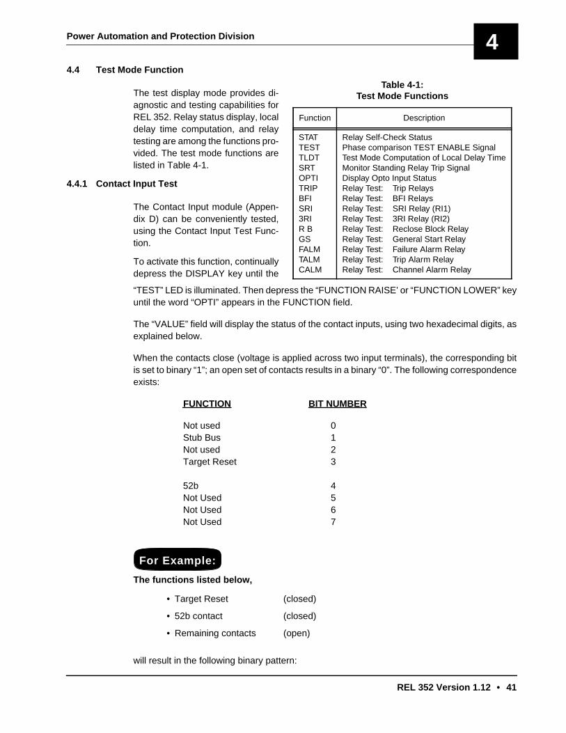
Power Automation and Protection Division
REL 352 Version 1.12 • 41
44.4 Test Mode Function
The test display mode provides di-agnostic and testing capabilities forREL 352. Relay status display, localdelay time computation, and relaytesting are among the functions pro-vided. The test mode functions arelisted in Table 4-1.
4.4.1 Contact Input Test
The Contact Input module (Appen-dix D) can be conveniently tested,using the Contact Input Test Func-tion.
To activate this function, continuallydepress the DISPLAY key until the
“TEST” LED is illuminated. Then depress the “FUNCTION RAISE’ or “FUNCTION LOWER” keyuntil the word “OPTI” appears in the FUNCTION field.
The “VALUE” field will display the status of the contact inputs, using two hexadecimal digits, asexplained below.
When the contacts close (voltage is applied across two input terminals), the corresponding bitis set to binary “1”; an open set of contacts results in a binary “0”. The following correspondenceexists:
FUNCTION BIT NUMBER
Not used 0Stub Bus 1Not used 2Target Reset 3
52b 4Not Used 5Not Used 6Not Used 7
For Example:
The functions listed below,
• Target Reset (closed)
• 52b contact (closed)
• Remaining contacts (open)
will result in the following binary pattern:
Table 4-1:Test Mode Functions
Function Description
STATTESTTLDTSRTOPTITRIPBFISRI3RIR BGSFALMTALMCALM
Relay Self-Check StatusPhase comparison TEST ENABLE SignalTest Mode Computation of Local Delay TimeMonitor Standing Relay Trip SignalDisplay Opto Input StatusRelay Test: Trip RelaysRelay Test: BFI RelaysRelay Test: SRI Relay (RI1)Relay Test: 3RI Relay (RI2)Relay Test: Reclose Block RelayRelay Test: General Start RelayRelay Test: Failure Alarm RelayRelay Test: Trip Alarm RelayRelay Test: Channel Alarm Relay
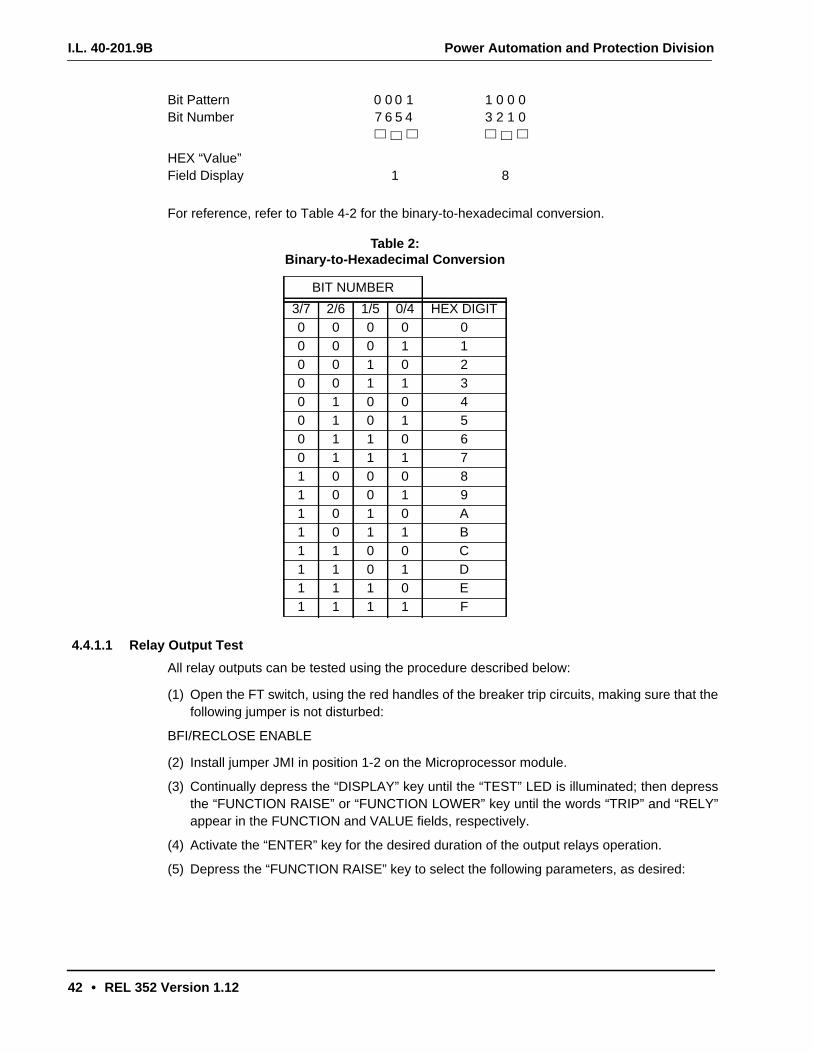
I.L. 40-201.9B Power Automation and Protection Division
42 • REL 352 Version 1.12
Bit Pattern 0 0 0 1 1 0 0 0Bit Number 7 6 5 4 3 2 1 0
HEX “Value”Field Display 1 8
For reference, refer to Table 4-2 for the binary-to-hexadecimal conversion.
Table 2:Binary-to-Hexadecimal Conversion
BIT NUMBER
3/7 2/6 1/5 0/4 HEX DIGIT0 0 0 0 00 0 0 1 10 0 1 0 20 0 1 1 30 1 0 0 40 1 0 1 50 1 1 0 60 1 1 1 71 0 0 0 81 0 0 1 91 0 1 0 A1 0 1 1 B1 1 0 0 C1 1 0 1 D1 1 1 0 E1 1 1 1 F
4.4.1.1 Relay Output Test
All relay outputs can be tested using the procedure described below:
(1) Open the FT switch, using the red handles of the breaker trip circuits, making sure that thefollowing jumper is not disturbed:
BFI/RECLOSE ENABLE
(2) Install jumper JMI in position 1-2 on the Microprocessor module.
(3) Continually depress the “DISPLAY” key until the “TEST” LED is illuminated; then depressthe “FUNCTION RAISE” or “FUNCTION LOWER” key until the words “TRIP” and “RELY”appear in the FUNCTION and VALUE fields, respectively.
(4) Activate the “ENTER” key for the desired duration of the output relays operation.
(5) Depress the “FUNCTION RAISE” key to select the following parameters, as desired:

Power Automation and Protection Division
REL 352 Version 1.12 • 43
4FUNCTION VALUE
FIELD FIELD DESCRIPTION
TRIP RELY TRIP (A, B, C)BFI RELY Breaker Failure InitiateSRI (RI1-1,2) RELY Reclose Initiate3RI (RI2-1,2) RELY Reclose InitiateRB RELY Recloser BlockingGS RELY General StartFALM RELY Failure AlarmTALM RELY Trip AlarmCALM RELY Channel Alarm
NOTE: Activate the “ENTER” key to operate selected output relays.
(6) After completion of this test, restore the system to its operating state by moving JM1 to po-sition 2-3 on the Microprocessor module, and closing the FT switch red handles.
4.4.2 Self Check
The results of the system self-check routines are accessible using the following procedure:
a. Continually depress the “DISPLAY” key until the “TEST” LED is illuminated; then depressthe “FUNCTION RAISE” or “FUNCTION LOWER” key until the word “STAT” appears in theFUNCTION FIELD.
b. The VALUE FIELD will display the status of the relay in hexadecimal Format:
RELAY STATUS
DESCRIPTION BIT NUMBER
External RAM Failure 0 ← Least SignificantEEPROM Failure 1 Right-Most
ROM Checksum Failure 2 PositionDual-Port RAM Failure 3
Analog Input Failure 4Processor Failure 5
± 12V P.S.Fail 6Modem Failure 7
EEPROM Warning 8Power Supply 1 Failure 9Power Supply 2 Failure 10
Dual Port RAMCom Status Warning 11
Failure Detected by Processor 1 12Failure Detected by Processor 2 13
0 14
0 15 ← Most SignificantLeft-Most
Position
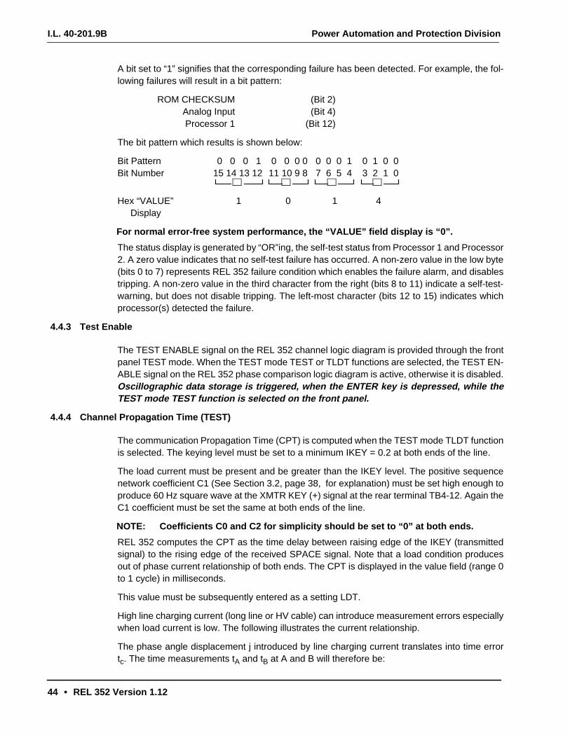
I.L. 40-201.9B Power Automation and Protection Division
44 • REL 352 Version 1.12
A bit set to “1” signifies that the corresponding failure has been detected. For example, the fol-lowing failures will result in a bit pattern:
ROM CHECKSUM (Bit 2)Analog Input (Bit 4)Processor 1 (Bit 12)
The bit pattern which results is shown below:
Bit Pattern 0 0 0 1 0 0 0 0 0 0 0 1 0 1 0 0Bit Number 15 14 13 12 11 10 9 8 7 6 5 4 3 2 1 0
Hex “VALUE” 1 0 1 4Display
For normal error-free system performance, the “VALUE” field display is “0”.
The status display is generated by “OR”ing, the self-test status from Processor 1 and Processor2. A zero value indicates that no self-test failure has occurred. A non-zero value in the low byte(bits 0 to 7) represents REL 352 failure condition which enables the failure alarm, and disablestripping. A non-zero value in the third character from the right (bits 8 to 11) indicate a self-test-warning, but does not disable tripping. The left-most character (bits 12 to 15) indicates whichprocessor(s) detected the failure.
4.4.3 Test Enable
The TEST ENABLE signal on the REL 352 channel logic diagram is provided through the frontpanel TEST mode. When the TEST mode TEST or TLDT functions are selected, the TEST EN-ABLE signal on the REL 352 phase comparison logic diagram is active, otherwise it is disabled.Oscillographic data storage is triggered, when the ENTER key is depressed, while theTEST mode TEST function is selected on the front panel.
4.4.4 Channel Propagation Time (TEST)
The communication Propagation Time (CPT) is computed when the TEST mode TLDT functionis selected. The keying level must be set to a minimum IKEY = 0.2 at both ends of the line.
The load current must be present and be greater than the IKEY level. The positive sequencenetwork coefficient C1 (See Section 3.2, page 38, for explanation) must be set high enough toproduce 60 Hz square wave at the XMTR KEY (+) signal at the rear terminal TB4-12. Again theC1 coefficient must be set the same at both ends of the line.
NOTE: Coefficients C0 and C2 for simplicity should be set to “0” at both ends.
REL 352 computes the CPT as the time delay between raising edge of the IKEY (transmittedsignal) to the rising edge of the received SPACE signal. Note that a load condition producesout of phase current relationship of both ends. The CPT is displayed in the value field (range 0to 1 cycle) in milliseconds.
This value must be subsequently entered as a setting LDT.
High line charging current (long line or HV cable) can introduce measurement errors especiallywhen load current is low. The following illustrates the current relationship.
The phase angle displacement j introduced by line charging current translates into time errortc. The time measurements tA and tB at A and B will therefore be:
Power Automation and Protection Division
REL 352 Version 1.12 • 45
4
tA = tD + tCtB = tD - tC
where tD is communication channel propagation delay adding above equations leads to:
tA + tB = 2 tDtD = tA + tD
2
Thus the error due to IC is eliminated.
4.4.5 Standing Relay Trip
A real-time status monitor of the Standing Relay Trip (SRT) logic signal is provided as a testmode function. The value of the SRT function is YES if any of the trip relays is enabled, other-wise, the value is “NO”.
! CAUTION
The user should verify that SRT = “NO” prior to putting the REL 352 in serviceafter testing.
5 JUMPER CONTROL
The following jumpers are set at the factory; the customer normally does not need to move thejumpers.
5.1 Backplane Module
An external jumper is permanently-wired to terminals 13/14 of switch 2FT-14.
When switch 2FT-14/13 or 2FT-14/14 is opened, the BFI and RI output relays are deenergizedto prevent BFI and RI contact closures during system function test.
5.2 Optoisolated Input module
5.2.1 Optoisolated Input module provides opto-isolated input interfaces from:
Optoisolated binary dc voltage Inputs 52b, STUB Bus, Target Reset to logic level inputs on theMicroprocessor module. This part contains 3 identical circuits, jumper positions JMP7 to JMP9.
IBIA
ICA BIA IB
IC ϕ
I.L. 40-201.9B Power Automation and Protection Division
46 • REL 352 Version 1.12
(1-2) are for 15/20 Vdc(3-4) are for 48/125 Vdc(5-6) are for 220/250 Vdc
Note: Position 3-4 is the factory setting.
5.3 Receiver Inputs
These inputs (SPACE 1, MARK 1, CHAN FAIL 1, SPACE 2, MARK 2, CHAN FAIL 2) interfaceto an external communication receiver such as Power Line Carrier, Audio Tone, etc.
Jumper Positions JMP1 to JMP6:1-2 are for 15/20 Vdc7-8 are for 48 Vdc9-10 are for 125 Vdc
Note: Position 1-2 is the factory setting.
5.4 Interconnect Module
5.4.1 Optoisolated Transistor Output for Communication Transmitter Keying
Selection for transmitter keying is provided by JMP7:
Position Voltage
1-2 125 Vdc3-4 48 Vdc5-6 15/20 Vdc
Factory setting is 5-6 (15/20 Vdc)
This interface also includes signal polarity inversion controlled by jumpers.
The Jumper assignments are:
JMP1 Channel FailJMP2 MARK 2JMP3 SPACE 2JMP4 MARK 1JMP5 SPACE 1JMP6 KEY OUT
5.5 Microprocessor Module
Jumper functions are listed below:
Jumper Position Description
JM1JM1
1-22-3*
Enable Relay Output TestDisable Relay Output Test(Normal Operation)
* Factory Setting
Position 1-2 Inverted (Factory setting)
Position 2-3 normal

Power Automation and Protection Division
REL 352 Version 1.12 • 47
4
6 NETWORK INTERFACE
Two options are available for interfacing between REL 352 and a variety of local and remotecommunication devices.
• RS-232C/PONI - for single point computer communication
• INCOM/PONI - for local network communication
An IBM PC or compatible computer, with software provided (WRELCOM), can be used to mon-itor the settings, 16 fault data records, 3 oscillographic records, and metering information. Fora remote setting, SETR should be set to “YES”; then the settings can be changed (remotely)with a user-defined password. If a user loses his assigned password, a new password can beinstalled by turning the REL 352 relay’s dc power supply “OFF” and then “ON”. REL 352 allowsa change of password within the next 15 minutes, by using a default “PASSWORD”.
When in the remote mode, the computer can disable the local setting by showing SET = REM(in the Metering mode). Then, the setting cannot be changed locally. In this situation, the onlyway to change a setting locally would be to turn the dc power “OFF” and then “ON”. The com-puter will allow for a local setting change within 15 minutes. Refer to the IL 40-603 (RemoteCommunication Program) for detailed information.
7 OSCILLOGRAPHIC DATA
Refer to ABB Publications:
• IL 40-603 Remote Communication Program (RCP)
• IL 40-606 Oscillographic and Recording Program (OSCAR)
8 REL 352 SETTINGS
The REL 352 setting mnemonics are in Table 4-3 (page 51); the appropriate setting informationis in Table 4-4 (page 53), i.e., setting name, format, setting range (min, max, step), units andrelated notes.
JM2JM2JM3JM4JM7JM8JM9
1-22-3*2-32-32-32-32-3
Disable Display SaverEnable Display SaverSpare, not used at this time“
““““
JM5JM5
1-22-3*
P2 RAM 2kx8P2 RAM 8kx8 or 32kx8
JM6JM6
1-2*2-3
P2RAM 32kx8P2 RAM 8kx8 or 2kx8
Jumper Position Description
* Factory Setting
I.L. 40-201.9B Power Automation and Protection Division
48 • REL 352 Version 1.12
9 MONITORING FUNCTIONS
The REL 352 monitoring functions display on-line system information (see Table 4-5, page 55)monitoring values and conditions are listed in Table 4-6 (page 56). All angles are computed us-ing VAG as the reference angle.
10 TARGET (FAULT DATA) INFORMATION
The REL 352 stores 16 sets of targets (fault data). All 16 sets are accessible through INCOM®,but only the two most recent sets of data are accessible from the front panel (see Table 4-5,page 55).
The first part of the fault data contains “Yes/No” targets (see Table 4-6, page 56), which identifythe cause of the trip and the status of certain system inputs and outputs; the second part of thefault data contains values, including currents, voltages, fault impedance, and distance to thefault.
11 ROUTINE VISUAL INSPECTION
With the exception of Routine Visual Inspection, the REL 352 relay assembly should be main-tenance-free. A program of Routine Visual Inspection should include:
• Condition of cabinet or other housing• Tightness of mounting hardware and fuses• Proper seating of plug-in relays and subassemblies• Condition of external wiring• Appearance of printed circuit boards and components• Signs of overheating in equipment
12 ACCEPTANCE TESTING
The customer should perform the REL 352 Acceptance Tests (see Appendix I, page 143) onreceipt of shipment.
13 NORMAL PRECAUTIONS
Troubleshooting is not recommended due to the sophistication of the Microprocessor unit.
! CAUTION
With the exception of checking to insure proper mating of connectors, or settingjumpers, the following procedures are normally not recommended. (If there is aproblem with the REL 352, it should be returned to the factory. See PREFACE.)
14 DISASSEMBLY PROCEDURES
a. Remove the inner chassis from the outer chassis, by unscrewing the two lockscrews(on the front panel), and unsnapping the two covers from the FT-14 switches.
Power Automation and Protection Division
REL 352 Version 1.12 • 49
415 FIRMWARE UPGRADE PROCEDURE
If it is necessary to upgrade the system firmware in your REL 352 relay system, it is easily ac-complished by changing out the 4 socketed EPROM I.C.s which contain the programs for the2 microprocessors.
After consulting the factory for the proper upgrade kit, just exchange the U01, U14, U31, andU46 EPROMS on the microprocessor module. Always be sure to confirm and adjust if neces-sary the relay settings after making any system version upgrade.
You will also need to use the latest version of the RCP communication software when makingversion upgrades to the relay system.
NOTE: a. The inner-chassis (sub-assembly) slides in and out of the outer chassisfrom the front. Mating connectors inside the case eliminate the need to dis-connect external wiring when the inner chassis is removed.
b. Remove the FT-14 switches, mounted by two screws on the side walls.
c. Remove the front panel (with the Display module) from the inner chassis,by unscrewing four screws behind the front panel.
d. Remove the Microprocessor module, by loosening six mounting screws,and unplugging the module from the Interconnect module.
e. Remove the Relay Output and Contact Input modules by unscrewing 2mounting screws from the brackets and unplugging these modules fromthe Interconnect module.
f. Remove the Power Supply and Analog Input modules, by first removingthe Microprocessor module and the support cross bar.
g. Remove the Backplate, by unscrewing the mounting hardware from therear of the Backplate.
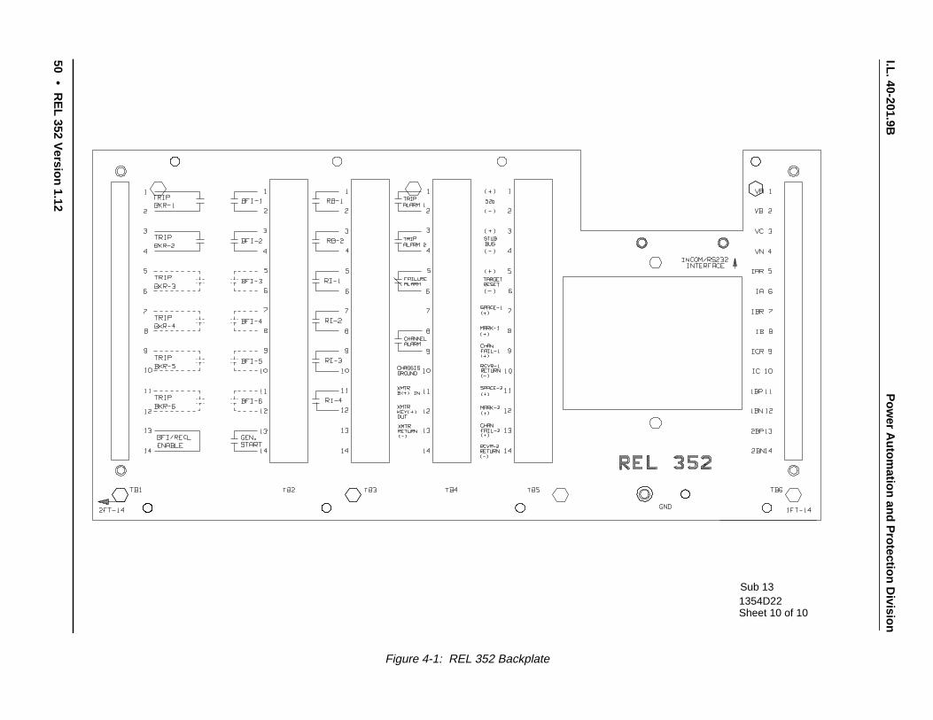
I.L. 40-201.9BP
ower A
utomation and P
rotection Division
50•
RE
L 352 Version 1.12
Sub 131354D22Sheet 10 of 10
Figure 4-1: REL 352 Backplate
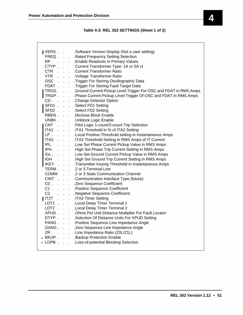
Power Automation and Protection Division
REL 352 Version 1.12 • 51
4
VERS . . . .Software Version Display (Not a user setting)FREQ . . . .Rated Frequency Setting SelectionRP . . . . .Enable Readouts In Primary ValuesCTYP . . . .Current Transformer Type: 1A or 5A ctCTR . . . .Current Transformer RatioVTR . . . .Voltage Transformer RatioOSC . . . .Trigger For Storing Oscillographic DataFDAT . . . .Trigger For Storing Fault Target DataTRGG . . . .Ground Current Pickup Level Trigger For OSC and FDAT in RMS AmpsTRGP . . . .Phase Current Pickup Level Trigger Of OSC and FDAT in RMS AmpsCD . . . . .Change Detector OptionSFD1 . . . .Select FD1 SettingSFD2 . . . .Select FD2 SettingRBEN . . . .Reclose Block EnableUNBK . . . .Unblock Logic EnableCNT . . . .Pilot Logic 1-count/2-count Trip SelectionITA1 . . . .ITA1 Threshold in % of ITA2 SettingLP . . . . .Local Positive Threshold setting in Instantaneous AmpsITA2 . . . .ITA2 Threshold Setting in RMS Amps of IT CurrentIPL . . . . .Low Set Phase Current Pickup Value in RMS AmpsIPH. . . . .High Set Phase Trip Current Setting in RMS AmpsIGL . . . . .Low Set Ground Current Pickup Value in RMS AmpsIGH . . . .High Set Ground Trip Current Setting in RMS AmpsIKEY . . . .Transmitter Keying Threshold in Instantaneous AmpsTERM . . . .2 or 3 Terminal LineCOMM . . .2 or 3 State Communication ChannelCINT . . . .Communication Interface Type (future)C0 . . . . .Zero Sequence CoefficientC1 . . . . .Positive Sequence CoefficientC2 . . . . .Negative Sequence CoefficientIT2T . . . .ITA2 Timer SettingLDT1 . . . .Local Delay Timer Terminal 1LDT2 . . . .Local Delay Timer Terminal 2XPUD . . . .Ohms Per Unit Distance Multiplier For Fault LocatorDTYP . . . .Selection Of Distance Units For XPUD SettingPANG . . . .Positive Sequence Line Impedance AngleGANG . . . .Zero Sequence Line Impedance AngleZR . . . . .Line Impedance Ratio (Z0L/Z1L)BKUP . . . .Backup Protection EnableLOPB . . . .Loss-of-potential Blocking Selection
**
Table 4-3: REL 352 SETTINGS (Sheet 1 of 2)
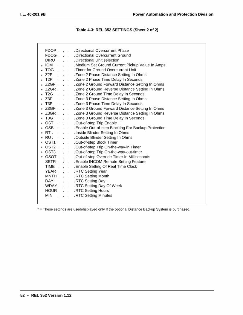
I.L. 40-201.9B Power Automation and Protection Division
52 • REL 352 Version 1.12
Table 4-3: REL 352 SETTINGS (Sheet 2 of 2)
FDOP . . . .Directional Overcurrent PhaseFDOG . . . .Directional Overcurrent GroundDIRU . . . .Directional Unit selectionIOM . . . .Medium Set Ground Current Pickup Value In AmpsTOG . . . .Timer for Ground Overcurrent UnitZ2P . . . .Zone 2 Phase Distance Setting In OhmsT2P . . . .Zone 2 Phase Time Delay In SecondsZ2GF . . . .Zone 2 Ground Forward Distance Setting In OhmsZ2GR . . . .Zone 2 Ground Reverse Distance Setting In OhmsT2G . . . .Zone 2 Ground Time Delay In SecondsZ3P . . . .Zone 3 Phase Distance Setting In OhmsT3P . . . .Zone 3 Phase Time Delay In SecondsZ3GF . . . .Zone 3 Ground Forward Distance Setting In OhmsZ3GR . . . .Zone 3 Ground Reverse Distance Setting In OhmsT3G . . . .Zone 3 Ground Time Delay In SecondsOST . . . .Out-of-step Trip EnableOSB . . . .Enable Out-of-step Blocking For Backup ProtectionRT . . . . . Inside Blinder Setting In OhmsRU . . . . .Outside Blinder Setting In OhmsOST1 . . . .Out-of-step Block TimerOST2 . . . .Out-of-step Trip On-the-way-in TimerOST3 . . . .Out-of-step Trip On-the-way-out-timerOSOT . . . .Out-of-step Override Timer In MillisecondsSETR . . . .Enable INCOM Remote Setting FeatureTIME . . . .Enable Setting Of Real Time ClockYEAR . . . .RTC Setting YearMNTH . . . .RTC Setting MonthDAY . . . .RTC Setting DayWDAY. . . .RTC Setting Day Of WeekHOUR. . . .RTC Setting HoursMIN . . . .RTC Setting Minutes
*****************
**
*
* = These settings are used/displayed only If the optional Distance Backup System is purchased.
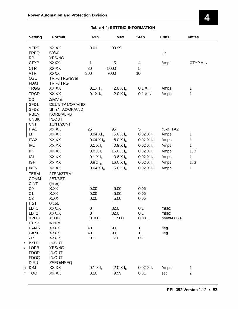
Power Automation and Protection Division
REL 352 Version 1.12 • 53
4Table 4-4: SETTING INFORMATION
Setting Format Min Max Step Units Notes
VERS XX.XX 0.01 99.99FREQ 50/60 HzRP YES/NOCTYP XXXX 1 5 4 Amp CTYP = InCTR XX.XX 30 5000 5VTR XXXX 300 7000 10OSC TRIP/ITRG/∆V∆IFDAT TRIP/ITRGTRGG XX.XX 0.1X In 2.0 X In 0.1 X In Amps 1
TRGP XX.XX 0.1X In 2.0 X In 0.1 X In Amps 1
CD ∆I/∆V ∆ISFD1 DELT/ITA1/OR/ANDSFD2 SIT2/ITA2/OR/ANDRBEN NORB/ALRBUNBK IN/OUTCNT 1CNT/2CNTITA1 XX.XX 25 95 5 % of ITA2LP XX.XX 0.04 XIn 5.0 X In 0.02 X In Amps 1
ITA2 XX.XX 0.04 X In 5.0 X In 0.02 X In Amps 1
IPL XX.XX 0.1 X In 0.8 X In 0.02 X In Amps 1
IPH XX.XX 0.8 X In 16.0 X In 0.02 X In Amps 1, 3
IGL XX.XX 0.1 X In 0.8 X In 0.02 X In Amps 1
IGH XX.XX 0.8 x In 16.0 X In 0.02 X In Amps 1, 3
IKEY XX.XX 0.04 X In 5.0 X In 0.02 X In Amps 1
TERM 2TRM/3TRMCOMM 2ST/3STCINT (later)C0 X.XX 0.00 5.00 0.05C1 X.XX 0.00 5.00 0.05C2 X.XX 0.00 5.00 0.05IT2T 0/150LDT1 XXX.X 0 32.0 0.1 msecLDT2 XXX.X 0 32.0 0.1 msecXPUD X.XXX 0.300 1.500 0.001 ohms/DTYPDTYP MI/KMPANG XXXX 40 90 1 degGANG XXXX 40 90 1 degZR XXX.X 0.1 7.0 0.1BKUP IN/OUTLOPB YES/NOFDOP IN/OUTFDOG IN/OUTDIRU ZSEQ/NSEQIOM XX.XX 0.1 X In 2.0 X In 0.02 X In Amps 1
TOG XX.XX 0.10 9.99 0.01 sec 2
**
**

I.L. 40-201.9B Power Automation and Protection Division
54 • REL 352 Version 1.12
Table 4-4: SETTING INFORMATION (SHEET 2 OF 2)
Setting Format Min Max Step Units Notes
Z2P XX.XX 0.01 50.00 0.01 ohms 4T2P XX.XX 0.00 2.99 0.01 sec 2Z2GF XX.XX 0.01 50.00 0.01 ohms 4Z2GR XX.XX 0.01 50.00 0.01 ohms 4T2G XX.XX 0.00 2.99 0.01 sec 2Z3P XX.XX 0.01 50.00 0.01 ohms 4T3P XX.XX 0.10 2.99 0.01 sec 2Z3GF XX.XX 0.01 50.00 0.01 ohms 4Z3GR XX.XX 0.01 50.00 0.01 ohms 4T3G XX.XX 0.10 2.99 0.01 sec 2OST NO/IWAYI/WAYOOSB NONE/Z2/Z3/BOTHRT XX.XX 1.00 15.00 0.10 ohms 4RU XX.XX 3.00 15.00 0.10 ohms 4OST1 XX.XX 0.50 5.00 0.05 cyclesOST2 XX.XX 0.50 5.00 0.05 cyclesOST3 XX.XX 0.50 5.00 0.05 cyclesOSOT XXXX 24 240 1 cycles 3SETR YES/NOTIME YES/NOYEAR XXXX 1980 2079 1 yearMNTH XX 1 12 1 monthDAY XX 1 31 1 dayWDAY SUN/MON/TUES/WED/THUR/FRI/SATHOUR XX 0 23 1 hourMIN XX 0 59 1 minute
NOTE 1: Current settings ranges are dependent upon the CTYP setting and the purchased CT option.The actual setting is always made in amps.
NOTE 2: These settings have a “BLK” option for disabling a corresponding function.
NOTE 3: These settings have an “OUT” option for disabling the protection.
NOTE 4: The impedance settings ranges are dependent upon the CTYP setting and the purchased option. The setting rang-es shown are for a 5 A ct. The setting range is multiplied by 5 if a 1 A ct is used (CTYP = 1).
**
*****
****
*
******
* = These settings are used/displayed only if the optional Distance Backup System is purchased.

Power Automation and Protection Division
REL 352 Version 1.12 • 55
4Table 4-5: MONITORING FUNCTIONS
FUNCTION DESCRIPTION FORMAT UNITS
CHRX . . . . REL 352 channel receive status ARM/CHTBCHTX. . . . . REL 352 channel transmit status KEYIA . . . . . . IA metered current magnitude . . . . . . . . XXX.X . . . Amps RMS
. . . . . IA metered current angle . . . . . . . . . XXXX. . . . degVAG . . . . . VAG metered voltage magnitude . . . . . . . XXX.X . . . Volts RMS
. . . . VAG metered voltage angle . . . . . . . . XXXX. . . . degIB . . . . . . IB metered current magnitude . . . . . . . . XXX.X . . . Amps RMS
. . . . . IB metered current angle . . . . . . . . . XXXX. . . . degVBG . . . . . VBG metered voltage magnitude . . . . . . . XXX.X . . . Volts RMS
. . . . VBG metered voltage angle . . . . . . . . XXXX. . . . degIC . . . . . . IC metered current magnitude. . . . . . . . XXX.X . . . Amps RMS
. . . . . IC metered current angle . . . . . . . . . XXXX. . . . degVCG . . . . . VCG metered voltage magnitude . . . . . . . XXX.X . . . Volts RMS
. . . . VCG metered voltage angle . . . . . . . . XXXX. . . . deg3I0 . . . . . 3I0 metered Current Magnitude . . . . . . . XXX.X . . . Amps RMS∠3I0 . . . . . 3I0 metered Current Angle. . . . . . . . . XXXX. . . . degDATE. . . . . Date (Month, Day) . . . . . . . . . . . MM/DDTIME . . . . . Time (Hours, Minutes) . . . . . . . . . . HH/MM . . . .SET . . . . . Setting access status . . . . . . . . . . BOTH/LOC/REMLOP . . . . . Loss-of-potential indication . . . . . . . . YES/NOLOI . . . . . Loss-of-current indication . . . . . . . . . YES/NOOSB . . . . . Out-of-step blocking indication . . . . . . . YES/NOIT . . . . . . IT metered current Magnitude. . . . . . . . XXX.X . . . Amps RMS
. . . . . IT metered current Angle . . . . . . . . . XXX.X . . . deg
NOTE: All angles are computed using V AG as the reference angle.
NOTE: RP setting determines whether the values will be displayed as primary or secondaryreadings. Primary readings are KV RMS and KA RMS for units.
* These functions are displayed only if the optional distance backup system is purchased and that system isactivated.
IA∠
VAG∠
IB∠
VBG∠
IC∠
VCG∠
***
IT∠

I.L. 40-201.9B Power Automation and Protection Division
56 • REL 352 Version 1.12
TARGET DESCRIPTION FORMAT UNITS
FTYP Fault Type AB/BG/CG/AB/BC/CA/ABCBK1 Phase A breaker current flowed YES/NOBK2 Phase B breaker current flowed YES/NOBK3 Phase C breaker current flowed YES/NOBK4 Phase A breaker current flowed YES/NOBK5 Phase B breaker current flowed YES/NOBK6 Phase C breaker current flowed YES/NOIAH High set phase A fault YES/NOIBH High set phase B fault YES/NOICH High set phase C fault YES/NOIGH High set ground fault YES/NOPLT Pilot trip YES/NORIFT Reclose-into-fault trip YES/NOSBT Stub-bus trip YES/NOOST Out-of-step trip YES/NOUNBK Unblock trip YES/NOTG Time overcurrent ground trip YES/NOZ2P Zone 2 phase fault YES/NOZ2G Zone 2 ground fault YES/NOZ3P Zone 3 phase fault YES/NOZ3G Zone 3 ground fault YES/NOZ Fault impedance XX.XX ohmsFANG Fault impedance angle XXX.X degDMI Fault distance in miles XXX.X milesDKM Fault distance in kilometers XXX.X kmPFLC Pre-fault load current XXX.X AmpsPFLV Pre-fault voltage XXX.X VoltsLP Pre-fault load angle XXX.X degVAG VAG fault voltage magnitude XXX.X Volts
VAG fault voltage angle XXX.X degVBG VBG fault voltage magnitude XXX.X Volts
VBG fault voltage angle XXX.X degVCG VCG fault voltage magnitude XXX.X Volts
VCG fault voltage angle XXX.X deg3V0 3V0 fault voltage magnitude XXX.X Volts
3V0 fault voltage angle XXX.X deg
*
*****
VAG∠
VBG∠
VCG∠
3V0∠
Table 4-6:TARGET (FAULT DATA) INFORMATION (SHEET 1 OF 2)
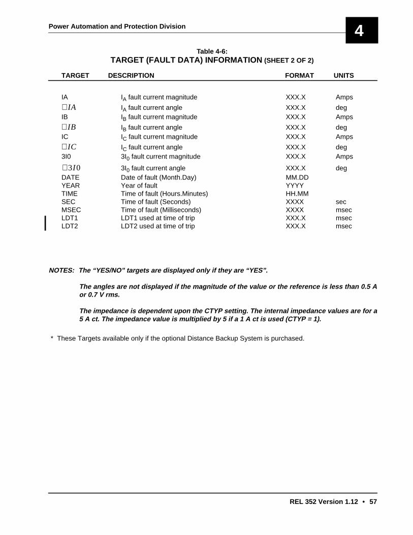
Power Automation and Protection Division
REL 352 Version 1.12 • 57
4
TARGET DESCRIPTION FORMAT UNITS
IA IA fault current magnitude XXX.X Amps
IA fault current angle XXX.X degIB IB fault current magnitude XXX.X Amps
IB fault current angle XXX.X degIC IC fault current magnitude XXX.X Amps
IC fault current angle XXX.X deg3I0 3I0 fault current magnitude XXX.X Amps
3I0 fault current angle XXX.X degDATE Date of fault (Month.Day) MM.DDYEAR Year of fault YYYYTIME Time of fault (Hours.Minutes) HH.MMSEC Time of fault (Seconds) XXXX secMSEC Time of fault (Milliseconds) XXXX msecLDT1 LDT1 used at time of trip XXX.X msecLDT2 LDT2 used at time of trip XXX.X msec
IA∠
IB∠
IC∠
3I 0∠
Table 4-6:TARGET (FAULT DATA) INFORMATION (SHEET 2 OF 2)
NOTES: The “YES/NO” targets are displayed only if they are “YES”.
The angles are not displayed if the magnitude of the value or the reference is less than 0.5 Aor 0.7 V rms.
The impedance is dependent upon the CTYP setting. The internal impedance values are for a5 A ct. The impedance value is multiplied by 5 if a 1 A ct is used (CTYP = 1).
* These Targets available only if the optional Distance Backup System is purchased.

I.L. 40-201.9B Power Automation and Protection Division
58 • REL 352 Version 1.12
THIS PAGE RESERVED FOR NOTES
Power Automation and Protection Division
REL 352 Version 1.12 • 59
5
1 INTRODUCTION
REL 352 can be set through the front panel Man-Machine Interface (MMI) or through RemoteCommunication Computer Software (WRELCOM Local Area Network).
This section will follow the sequence of settings displayed in the front panel display when therelay system is in the settings mode. Reference will be made to current levels based on 5A sec-ondary line ct’s.
! CAUTION
For 1A secondary line ct’s multiply the current levels by 0.2.For 50 Hz the timers are 20% longer unless stated on logic diagrams.
2 RELAY SYSTEM SET UP
2.1 Software Version (Vers)
Indicates the software version in the REL 352 (read only).
2.2 System Frequency (FREQ)
Select either 60 or 50 Hz, depending on the power system frequency.
NOTE: It is imperative that the proper selection of frequency is made prior to applica-tion of power system currents and voltage.
2.3 Readout in Primary Values (RP)
A “YES” setting enables the REL 352 system to display all the monitored voltages and currentsin primary kAmperes and kVolts.
2.4 Current Transformer Type (CTYP)
This setting must be set according to the catalog number of the relay.
For Example
Enter CTYP = 5 if the relay has been purchased with the 5A ct option.
2.5 Current Transformer Ratio (CTR)
This setting is used for load current monitoring, if it is selected to be displayed in primary kAm-peres. It has no effect on the protective relaying system.
For Example
Set CTR = 240 if 1200/5 line ct’s are being used.
Section 5. SETTING CALCULATIONS
I.L. 40-201.9B Power Automation and Protection Division
60 • REL 352 Version 1.12
2.6 Voltage Transformer Ratio (VTR)
This setting is used for the system voltage monitoring, if it is selected to be displayed in primarykVolts. It has no effect on the protective relaying system.
For Example
Set VTR = 575 if 69000 V to 120 V vt’s are being used.
3 OSCILLOGRAPHIC INFORMATION
3.1 Trigger for Storing Oscillographic Data (OSC)
Indicates trigger for oscillographic data gathering. The user can select the trigger of oscillo-graphic data when:
• TRIP — The REL 352 system tripped
• ITRG — The REL 352 system detected the operation of either the TRGP orTRGG, phase or ground current trigger respectively (see below).
• ∆V, ∆I — The REL 352 system has detected a fault in the system that may noteven be within the protective zone of the relay
The change detector occurs when current or voltage change between the corresponding datasamples, spaced one power line cycle apart, exceeds 12.5%.
Using of CD as a trigger of oscillographic data is of little practical value when a relay is connect-ed to a “live” power system.
Numerous changes due to sudden load changes, remote switching, distant faults, etc., makethe resulting oscillographic records difficult to relate to events of importance.
3.2 Ground Trigger Pick UP Level (TRGG)
This setting controls the level of current magnitude, on the ground current, to start oscillograph-ic data gathering.
3.3 Phase Trigger Pick Up Level (TRGP)
This setting controls the level of current magnitude, on the phase currents to start oscillographicdata gathering.
4 PHASE COMPARISON - LOGIC SETTINGS
4.1 Change Detector Option (CD)
The Change Detector (CD) is used for the following:
• Supervision of Trip Function.
• Enabling of Transmitted IKEY for ON-OFF Power Line Carrier Applications.
• Supervision of Unblock Logic.
All relay current inputs (IA, IB, IC and IG) and voltage inputs (VA, VB and VC) are sampled (con-
verted to numbers) 12 times per Power Line Cycle. The present samples are compared to thecorresponding samples taken 1 cycle “ago”.
Power Automation and Protection Division
REL 352 Version 1.12 • 61
5The change detector is asserted if the absolute difference of present and old sample exceeds12.5% of the old sample and the difference is greater than:
• 1 pu for current - 0.1 x 5 = 0.5A
• 7V for voltage
The CD can be generated either by using the current change detectors (∆I) or the current andvoltage change detectors (∆I and ∆V).
The user can select the generation of change detector on:
• ∆I — Current change detectors only. This setting provides more security.
• ∆I ∆V — Current and voltage change detectors if the system has voltage inputs.This setting provides more sensitivity and should always be used forweak-feed applications, where the change in current may not be signifi-cant to start the relaying system.
4.2 Fault Detectors (FD1 and FD2)
The fault detectors supervise trip. In addition, FD1 is used for supervision of keying in an ON/OFF PLC system. The fault detectors are computed by converting the symmetrical componentfilter output to its rms equivalent and comparing it versus the set level, ITA1 and ITA2. The faultdetectors can also be activated by current change functions (DIT1 and DIT2) which have fixedsettings of 6% and 12% (respectively).
The setting possibilities for FD1, which are selected by the SFDi (select FD1) setting are:
ITA1 ITA1 IT rms current level detector onlyDELT DIT1 IT instantaneous 6% IT current change fault detector or CD 12% input current
change detectorOR either ITA1 OR DELTAND both ITA1 AND DELT
The recommended setting is ITA1 for FSK systems. For ON/OFF carrier systems ITA1. If ITA1is set higher than minimum fault current, the OR setting is recommended. FD2 is used to enablephase comparison. The relay is blocked unless FD2 picks up.
The setting possibilities for FD2, which are selected by the SFD2 (select FD2) setting are:
ITA2 ITA2 IT rms current level detector onlyDIT2 DIT2 instantaneous 12% IT current change fault detectorOR either ITA2 OR DIT2AND both ITA2 AND DIT2
The recommended setting is ITA2 for FSK systems. For ON/OFF systems if ITA2 is set higherthan minimum fault current, the OR setting is recommended.
4.3 Reclose Block Enable (RBEN)
The following settings are provided for system flexibility:
- NORB No Reclose Block for the system. The logic may be provided by external devices.
- ALRB Reclose Block will be activated for all types of faults.

I.L. 40-201.9B Power Automation and Protection Division
62 • REL 352 Version 1.12
4.4 Unblock Logic Enable (UNBK)
The Unblock Logic may be used for FSK applications. UNBK = IN allows tripping for a 150 msecwindow following loss-of-channel if the current exceeds the ITA2 setting. In addition, the Un-block Logic includes a function to allow trip for loss of channel during reclosing conditions.
4.5 Phase Comparison Count (CNT)
This setting provides a choice between security and speed. The options are:
- 1CNT Only one 4 msec trip comparison is required to trip the system.
- 2 CNT If the coincidence is only 4 - 6 msec long a second coincidence greater than 4msec is required within 25 msec (for FSK PLC) or 40 msec (for ON/OFF PLC). Ifthe output is longer than 6 msec, no second comparison is required.
For higher security, set CNT = 2CNT. However, it should be noted that for ON/OFF PLC appli-cations, comparison is made on the negative half cycle only. A 2 CNT setting might result inundesirable long maximum operating times.
4.6 ITA2 Fault Detector Pulse Stretch Setting (IT2T)
When FD2 is set to DIT2, or OR, it is advisable to set IT2T = 150. This will ensure that the faultdetector FD2 stays picked up for 150 msec after being asserted by the current change detectorDIT2. When SFD2 is set to ITA2, or AND, setting of IT2T = 0 is recommended.
4.7 Current Level Setting for ITA1 Element)
ITA1 element detector measures the rms output of the sequence filter, IT. ITA1 picks up when-ever the IT rms current exceeds the ITA1 setting times the ITA2 setting.
The ITA1 threshold setting is set in percentage of ITA2 current level. ITA1 should be set moresensitive than ITA2 and a setting of 80% is recommended. ITA1 is an IT rms threshold setting.
4.8 Local Positive Level (LP)
This setting determines the local squarewave generation as shown in section 3, 2.1 (Local Pos-itive (LP) and Local Negative (LN) on page 15) and figure 3-3 (page 23).
Notice that the local negative level LN is internally computed from LN = -LP.
Due to system security the recommended LP setting should be 2.0 X IKEY setting.
4.9 Current Level Setting for ITA2 Element
ITA2 element detector measures the rms output of the sequence filter, IT. ITA2 is an IT rmsthreshold setting. ITA2 element picks up whenever the IT rms current exceeds the ITA2 setting.
The recommended setting is:
1) For FSK PLC applicationsITA2 ≤0.7 ITmin
where
ITmin is the minimum current out of the sequence filter for an internal fault. The minimum
IT current is normally determined by the minimum three phase fault current multiplied by
Power Automation and Protection Division
REL 352 Version 1.12 • 63
5the setting coefficient C1. The 30% margin between ITA2 and ITmin ensures relaible op-
eration for all internal faults.
2) For ON/OFF PLC applicationsITA2 ≥1.1 ITload
where
ITload is the maximum load current out of the sequence filter, i.e., the maximum load cur-
rent multiplied by the setting coefficient C1. In case the ITA2 current level will be higherthan minimum IT produced by an internal fault, SFD2 should be set to OR in order to en-able trip from the instantaneous IT current change detector DIT2 (see 4.2 above).
4.10 Low Set Phase Unit (IPL)
The low set overcurrent units perform supervision of the phase comparison trip logic and thestub bus trip. To prevent tripping from the stub bus logic during line energization, the IPL shouldbe set higher than 1.5 times the net line charging current. A minimum setting of 0.5 A is recom-mended.
The line charging current is here defined as the steady state net single-end line charging phasecurrent, as measured under balanced conditions (all local poles closed and all remote polesopen). “Net” line charging current indicates the distributed capacitive current minus any line-connected shunt reactor current, since line-connected shunt reactors are within the zone of pro-tection and tend to cancel the capacitive current.
4.11 High Set Phase Overcurrent Unit (IPH)
The high set phase overcurrent unit supplements the phase comparison protection by providinga non-pilot direct trip capability for high current internal faults. The IPH unit should be set for1.25 times the maximum through current for an external three-phase fault.
The high set overcurrent units can be made directional when FDOP is set to IN, and threephase voltage is applied to the relay. IPH is then supervised by FDOP.
4.12 Low Set Ground Unit (IGL)
The ground unit supervises the phase comparison system in parallel with the Low Set PhaseUnit. since the effect of charging current is minimal for the ground current, the setting need onlyto allow for inherent unbalance during normal operation. A minimum setting of 0.5 A is recom-mended.
4.13 High Set Ground Overcurrent Unit (IGH)
The setting of the high set ground unit should follow the same guidelines as the high set phaseunits. The IGH unit can be made directional by setting FDOG to IN, and connecting three phasevoltage to the relay. IGH is then supervised by FDOG.
4.14 Transmit Keying Level (IKEY)
IKEY defines the threshold generating the square wave to be set to the remote terminal. Pleasebe aware that the I waveform from which this transmitted signal is generated is the function ofcoefficients described in section 4.17 (Symmetrical Component Coefficients C0, C1 and C2).
I.L. 40-201.9B Power Automation and Protection Division
64 • REL 352 Version 1.12
IKEY should be larger than 1.5 times the maximum charging current multiplied by C1, i.e.,IKEY > 1.5 •C1•I CHmax
A minimum setting of 0.3 A (6% of nominal current) is recommended.
The IKEY setting is an instantaneous threshold, which when exceeded by “IT” causes the IKEYoutput to a logic “1” state.
4.15 Number of Line Terminals (TERM)
This setting determines the number of line terminals for a FSK PLC system. For normal 2 ter-minal line TERM = 2, for three terminal line TERM = 3.
For ON/OFF PLC application the setting should always be TERM = 2, even for a three terminalline. The ON/OFF application is a blocking system why all terminals operate over the samecommunication channel.
4.16 Communication Channel Type (COMM)
For ON/OFF Power Line Carrier select COMM = 2.The phase comparison is made on negative half cycles only.
For FSK PLC set COMM = 3.COMM = 3 allows phase comparison on both positive and negative half cycles.
4.17 Communication Interface Type (CINT)
Reserved for future use. The setting is fixed, CINT = BIO (Binary I/O)
4.18 Symmetrical Component Coefficients (C0, C1, C2)
REL352 uses sequence filters to obtain positive, negative and zero sequence currents. Thesecurrents are then combine into one quantity:
IT = C0•I0 - C1•I1 + C2•I2
where
I0, I1 and I2 is the zero sequence, the positive sequence and the negative sequence currents.
In order to minimize the influence of load, C1 should be set to a relatively low value, we recom-mend to use C1 = 0.1. C0 and C2 will both multiply fault currents. Setting recommendations C1and C2 for three cases are made:
Case 1) Minimum fault current for a ground fault > 50% of minimum fault current for a threephase fault.
Case 2) Minimum fault current for a ground fault < 50% of minimum fault current for a threephase fault.
Case 3) Minimum fault current for a ground fault < 12.5% of minimum fault current for a threephase fault.
Case 1
Either C2 or C0 can be used for fault detection of any unsymmetrical fault. The use of negativesequence, C2, is preferable as the negative sequence currents are more consistent at the twoline terminals. We therefore recommend setting C0 = 0.

Power Automation and Protection Division
REL 352 Version 1.12 • 65
5High values of C2 increase the sensitivity. To minimize the relay’s response to system unbal-ances a “moderate” setting is recommended. Good sensitivity with high security is achieved withsetting C2 = 0.7.
The recommended settings:
C1 = 0.1C2 = 0.7C0 = 0.0gives the following sensitivity for different faults:
Three phase faults
Single phase to ground faults
Case 2
When the minimum ground fault current is substantially smaller than the minimum three phasefault current, C0 can be given a value to increase the sensitivity for ground fault.
The recommended settings
C1 = 0.1C2 = 0.7
C0 = according to Figure 1
gives the following sensitivity for different faults:
Three phase faults
Phase-phase faults
Single phase to ground faults
The value of C0 is determined from Figure 1. Calculate the ratio I3Φmin/IΦGmin and find this num-
ber on the vertical axis. Find the C0 for the calculated current ratio based on the curve corre-sponding to the least sensitive fault type.
Selecting C0 is this way results in the same sensitivity for minimum ground fault current as forminimum three phase fault current.
ITmin C1 I 3φmin⋅– 0.1 I 3φmin⋅–= =
ITmin1
3-------( C1– C2 e
j60°±)⋅+ I φφmin⋅ 3.8 I φφ⋅ 3.8
32
------- I 3φmin⋅ ⋅ 3.3 I 3φmin⋅= = = =
I Tmin13---( C1– C2 C0)+ + I φGmin⋅ 0.2 I φGmin⋅= =
min3min3min 1.01 φφ IICIT ⋅−=⋅−=
min3min3minmin60
min 3.32
38.38.3)21(
3
1φφφφφφ IIIIeCCIT j ⋅=⋅⋅=⋅=⋅⋅+−= ± o
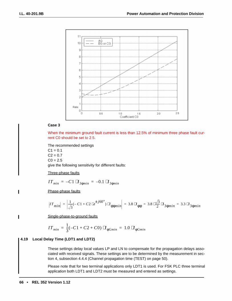
I.L. 40-201.9B Power Automation and Protection Division
66 • REL 352 Version 1.12
Case 3
When the minimum ground fault current is less than 12.5% of minimum three phase fault cur-rent C0 should be set to 2.5.
The recommended settingsC1 = 0.1C2 = 0.7C0 = 2.5give the following sensitivity for different faults:
Three-phase faults
Phase-phase faults
Single-phase-to-ground faults
4.19 Local Delay Time (LDT1 and LDT2)
These settings delay local values LP and LN to compensate for the propagation delays asso-ciated with received signals. These settings are to be determined by the measurement in sec-tion 4, subsection 4.4.4 (Channel propagation time (TEST) on page 50).
Please note that for two terminal applications only LDT1 is used. For FSK PLC three terminalapplication both LDT1 and LDT2 must be measured and entered as settings.
ITmin C1 I 3φmin⋅– 0.1 I 3φmin⋅–= =
ITmin1
3-------( C1– C2 e
j60°±)⋅+ I φφmin⋅ 3.8 I φφ⋅ 3.8
32
------- I 3φmin⋅ ⋅ 3.3 I 3φmin⋅= = = =
ITmin13---( C1– C2 C0)+ + I φGmin⋅ 1.0 I φGmin⋅= =
Power Automation and Protection Division
REL 352 Version 1.12 • 67
55 FAULT LOCATOR, BLINDERS AND
DISTANCE PROTECTION COMMON SETTINGS
5.1 Ohms per Unit Distance (XPUD)
This setting is used by the fault locator algorithm to estimate a calculated distance to the fault.The units of XPUD will be in primary ohms per mile or ohms per kilometer, depending on thesetting of DTYP.
For Example
Set XPUD = 0.8 if DTYP = miles and the line reactance is 0.8 Primary Ohms/mile.
5.2 Distance Unit Type for XPUD (DTYP)
Either miles (MI) or kilometers (km) should be selected. This setting should match the unitsused in XPUD.
5.3 Line Positive sequence impedance setting angle (PANG)
This setting relates directly to the assumed positive sequence impedance angle of the line. Itdefines the Zone 2 and Zone 3 phase impedance unit maximum torque angle in degrees. Thissetting is also the complement of ZP (Phase reach) and is also used for defining the slope ofthe blinders for OST and OSB and for the fault locator algorithm.
For example, if the assumed positive sequence impedance of the line is Z1 = 3.0 ohms at 75°,then set PANG = 5
5.4 Line zero sequence impedance angle setting (GANG)
This setting defines the assumed impedance angle of the zero sequence (Zl0) impedance ofthe transmission line. Zone 2 and Zone 3 ground impedance units use this parameter for theiroperation.
For Example
If the assumed zero sequence impedance of the line is Zl0 = 15 ohms at 80° then setGANG = 80.
5.5 Zero sequence impedance to Positive sequence impedance ratio (ZR)
This setting is used for all ground fault measurements. It reflects the magnitude ratio of the as-sumed zero sequence impedance to the positive sequence impedance of the line.
For Example
If Zl0 = 65 ohms at 60°, and Zl1 = 19 ohms at 75°, then set ZR = 65/19 = 3.42.

I.L. 40-201.9B Power Automation and Protection Division
68 • REL 352 Version 1.12
6 OPTIONAL BACK - UP SYSTEM SETTINGS
6.1 Loss of Potential Block enable (LOPB)
This setting enables the loss of potential logic (Vo and not Io) to block all Zone 2 and Zone 3impedance units if the logic is satisfied.
For Example
Set LOPB = YES to enable the logic.
6.2 Forward Directional Phase Unit (FDOP)
If the system has voltage inputs, then the high set overcurrent units (IPH) can be made direc-tional if FDOP is in. Set FDOP = IN to make the IPH units directional.
6.3 Forward Directional Ground Unit (FDOG)
If the system has voltage inputs, then the high set overcurrent unit (IGH) and the time delayedground back-up unit (TOG) can be made directional if FDOG is in. Set FDOG = N to the makethe IGH and TOG units directional.
6.4 Ground Directional Unit Polarization Options (DIRU)
The ground directional unit can be zero sequence or negative sequence polarized. When zerosequence polarized it uses all zero sequence quantities to determine the power flow directionand it is very sensitive to zero sequence mutuals between parallel lines. When negative se-quence polarized it uses all negative sequence quantities to determine the power flow directionand its operation is negligibly affected by the presence of mutual effects. Set DIR = ZSEQ if mu-tuals are not a consideration and DIR = NSEQ if strong zero sequence mutuals are present inthe neighborhood of the transmission line.
6.5 Medium Set Zero Sequence Overcurrent Unit (IOM)
This overcurrent unit supervises the ground trips of the ground units in the impedance back-upsystem. If TOG is being used it is also used for tripping after a time delay, TOG. It is measuringthe ground return current or 3Io. It should be set above the maximum expected unbalance inthe normal load current flow in the line.
The recommended setting is IOM = 0.5 amps.
7 ZONE 2 AND ZONE 3 SETTINGS
Settings for Zone 2 and Zone 3 protective systems are similar. Application of the distance unitsfollow the standard application for a conventional step distance, non-pilot relaying system.
The impedance units are always to be used as time delayed Zone 2 and Zone 3 protectivezones.
Following the traditional step distance, Zone 2 is set to under-reach any Zone 1 covering theadjacent lines coming out of the remote terminal, if possible. It is also expected that Zone 2 willalways cover at least 100 percent of the protected line plus 10 percent of the shortest adjacentline under all operating conditions.

Power Automation and Protection Division
REL 352 Version 1.12 • 69
5Zone 2 timers, for phase and ground, should be set to coordinate with the forward and reverseadjacent high speed trips. Moreover, the timer should include the breaking time of the slowestadjacent breaker and a tolerance of two to three cycles. Typical Zone 2 timers range between0.2 to 0.3 seconds.
For Zone 3, it is recommended to be set under-reaching any Zone 2 from the remote terminal,if possible . Zone 3 should include at least 100 percent of the protected line plus 100 percentof the adjacent shortest line plus 10 percent of the next shortest line.
Zone 3 timers, for phase and ground, should be set to coordinate with the forward and reverseadjacent Zone 2 trips. Generally two times the Zone 2 timer may be chosen for the Zone 3 timersetting. Zone 3 timer ranges between 0.4 and 0.6 seconds.
Applicable parameters and settings for the characteristics of the zones have been discussedalready. These are the PANG, GANG and ZR settings discussed in previous paragraphs sincethey are commonly used in other parts of the relay algorithms, for example the fault locator.
Ground units in both zones have a forward (ZGf) and a reverse (ZGr) reach. Therefore, phaseto ground, three phase and some phase to phase to ground faults have a forward and a reversereach.
The phase to phase unit in REL 352 has only a forward reach (ZP). This unit is inherently di-rectional and its characteristics, which are dependent on the source impedance. This impliesthat all phase to phase and some phase to phase to ground faults have a forward reach onlydetermined by the phase to phase unit.
7.1 Zone 2 Phase Unit Reach (Z2P)
This setting controls the Zone 2 reach for phase to phase faults in secondary ohms. It is alwaysforward looking.
For Example
If Z2 reach is 30 ohms at 75°, set Z2P = 30.
7.2 Zone-2 Phase Timer (T2P)
Selects the time delay for Zone 2 Phase fault detection in seconds. Set T2P = 0.15 if the min-imum time delay for step distance coordination is 150 milliseconds.
7.3 Forward Zone 2 Ground Unit Reach (Z2GF)
This setting is equivalent to the phase unit setting since it defines the forward reach of the Zone2 ground unit in secondary ohms.
For Example
Set Z2GF = 30 if the Zone 2 reach is 30 ohms at 75°.
7.4 Reverse Zone 2 Ground Unit Reach (Z2GR)
Phase to ground units in REL 352 have been designed to have a definite reverse looking reach.This makes the phase to ground units non-directional.
I.L. 40-201.9B Power Automation and Protection Division
70 • REL 352 Version 1.12
For Example
If the reverse reach has been determined to be 15 ohms at 75°, set Z2GR = 15.
7.5 Zone 2 Ground Unit Timer (T2G)
Selects the time delay for Zone 2 Ground fault detection in seconds. Set T2G = 0.15 if the min-imum time delay for step distance coordination is 150 milliseconds.
7.6 Zone 3 Phase Unit Reach (Z3P)
This setting controls the Zone 3 reach for phase to phase faults in secondary ohms. It is alwaysforward looking.
For Example
If Z3 reach is 45 ohms at 75°, set Z3P = 45.
7.7 Zone-3 Phase Timer (T3P)
Selects the time delay for Zone 3 Phase fault detection in seconds. Set T3P = 0.30 if the mini-mum time delay for step distance coordination is 300 milliseconds.
7.8 Forward Zone 3 Ground Unit Reach (Z3GF)
This setting is equivalent to the phase unit setting since it defines the forward reach of the Zone3 ground unit in secondary ohms.
For Example
Set Z3GF = 45 if the Zone 3 reach is 45 ohms at 75°.
7.9 Reverse Zone 3 Ground Unit Reach (Z3GR)
Phase to ground units in REL 352 have been designed to have a definite reverse looking reach.This makes the phase to ground units non-directional.
For Example
If the reverse reach has been determined to be 15 ohms at 75°, set Z3GR = 15.
7.10 Zone 3 Ground Unit Timer (T3G)
Selects the time delay for Zone 3 Ground fault detection in seconds. Set T3G = 0.30 if the min-imum time delay for step distance coordination is 300 milliseconds.
8 OPTIONAL OUT OF STEP LOGIC SETTINGS
Phase comparison system is immune to system swings. When the optional backup distancesystem is purchased with the REL 352, blinders are provided for power swing detection. TheOut of Step Trip (OST) logic is executed all the time regardless of the status of the channel.

Power Automation and Protection Division
REL 352 Version 1.12 • 71
5This means that OST is possible when the system is operating the phase comparison algorithmonly. The Out of Step Block (OSB) logic is only applicable to the back-up system, i.e., Zone 2and Zone 3.
8.1 Out of Step Trip (0ST)
This setting enables the Out of Step Trip logic. Set the relay to:
OUT: If there is no need for an Out of Step Trip.
WAYI: If the controlled Out of Step Trip is in the Way in to the operating characteristics ofthe relay.
WAYO: If the controlled Out of Step Trip is in the Way out of the operating characteristics ofthe relay.
8.2 Out of Step Block (OSB)
This setting enables the Out of Step Block logic that blocks the Zone 2 and/or Zone 3 distanceunits under Out of Step Conditions.
Chose:
OUT: If no OSB is required
Z2: If only Zone 2 units are to be blocked by the OSB logic on Out of Step conditions.
Z3: If only Zone 3 units are to be blocked by the OSB logic on Out of Step conditions.
BOTH: If both Zone 2 and Zone 3 are to be blocked by the OSB logic on Out of Step condi-tions.
8.3 Inner Blinder, 21 BI, Setting (RT)
This setting is the offset in the perpendicular direction to the line impedance on the R-X diagramin Ohms.
For Example
Set RT = 4.0 ohms for an inner blinder 4 ohms away from the line impedance.
NOTE: RT restricts tripping inside its operating characteristics. It may be used forload restriction purposes to avoid tripping under load.
8.4 Outer Blinder, 21 BO, Setting (RU)
Similar to RT. It does not restrict tripping. Used mainly to detect out of step conditions.
For Example
Set RU = 8.0 ohms for a blinder 8.0 ohms away from the line impedance.

I.L. 40-201.9B Power Automation and Protection Division
72 • REL 352 Version 1.12
8.5 Out Of Step Detection Timer (OST1)
This timer is started when the outer blinder, 21 BO, has operated but the inner blinder, 21 BI,has not operated. If the timer times out, an out of step condition has been detected and OSB isactive.
For Example
Set OST1 = 1.5 cycles.
8.6 Out Of Step Trip On The Way In Timer (OST2)
This timer is started when an Out of Step condition has been detected and the two blinders haveoperated. Once it times out, a trip signal is issued for OST.
For Example
Set OST2=2 cycle.
8.7 Out Of Step Trip On The Way Out Timer (OST3)
This timer is started when an Out of Step condition has been detected and the OST2 timer hastimed out and both 21 BI are NOT operated. This permits controlling the time that the breakeropens.
OST3 = 0.5 cycles
8.8 Out Of Step Over-ride Timer (OSOT)
This timer is started once an Out of Step condition is identified (output of OST1). An OST signalis generated if OSOT times out and the apparent impedance seen by the relay is inside Zone2 or Zone 3 reach plus the RT blinde
For Example
OSOT = 1600 msec
9 TIME SETTINGS
REL 352 has an internal clock for event time tagging purposes. Even if the unit has lost its pow-er supply the internal clock will continue running.
9.1 Setting The Clock
To set the clock in the relay, set TIME = YES.The next fields are self explanatory:
- Year YEAR - Month MNTH- Day DAY - Day of the week WDAY- Hour HOUR - Minutes MIN
Enter the correct values as appropriate.

Power Automation and Protection Division
REL 352 Version 1.12 • 73
5Please note that if IRIG-B option on RS232 PONI is used, the clock will be updated continuous-ly as broadcasted by IRIG Network.

I.L. 40-201.9B Power Automation and Protection Division
74 • REL 352 Version 1.12
THIS PAGE RESERVED FOR NOTES

Power Automation and Protection Division
REL 352 Version 1.12 • 75
GLOSSARY
TERM DESCRIPTION
-3IO TRACE Displays the analog waveform of the -3IO current input current
∠ 3IO METERING 3IO metered current phase angle in degrees
∠ 3IO TARGET 3IO fault current angle in degrees
∠ IA METERING phase A metered current phase angle in degrees
∠ IA TARGET Phase A fault current angle in degrees
∠ IB METERING Phase B metered current phase angle in degrees
∠ IB TARGET Phase B fault current angle in degrees
∠ IC METERING Phase C metered current phase angle in degrees
∠ IC TARGET Phase C fault current angle in degrees
∠ VA METERING Phase A metered voltage phase angle in degrees
∠ VAG TARGET Phase A fault voltage angle in degrees
∠ VB METERING Phase B metered voltage phase angle in degrees
∠ VBG TARGET Phase B fault voltage angle in degrees
∠ VC METERING Phase C metered voltage phase angle in degrees
∠ VCG TARGET Phase C fault voltage angle in degrees
21BI ELEMENT Operates when measured impedance is within the RT reach setting (optional)
21BI TRACE Displays pickup of the 21BI inner blinder element (optional)
21BO ELEMENT Operates when measured impedance is within the RU reach setting (optional)
21BO TRACE Displays pickup of the 21BO outer blinder element (optional)
3IO METERING 3IO metered current magnitude in rms amps
3IO TARGET 3IO fault current magnitude in rms amps
52b INPUTThe dc voltage input into the relay which should be energized whenever the line breakeris tripped
52b SIGNAL The logic signal for the 52b input after optical input buffering
52b TRACE Displays the 52b signal
A2 SIGNAL The output of the ITA2 element
A2 TRACE Displays the output of the ITA2 element before the pulse stretch timer
AGF TRACE AG fault. Operates whenever the phase selector element determines fault type to be AG
ARM METERING Channel receive status = channel armed
BFI SIGNAL The breaker failure initiate signal
BFI TRACE Displays the BFI signal
I.L. 40-201.9B Power Automation and Protection Division
76 • REL 352 Version 1.12
BFI-1 OUTPUTCONTACTS
Breaker failure initiate 1. A pair of output contacts which close whenever the BFI signal isactivated
BFI-2 OUTPUTCONTACTS
Breaker failure initiate 2. A pair of output contacts which close whenever the BFI signal isactivated
BFI-3 OUTPUTCONTACTS
Breaker failure initiate 3. A pair of output contacts which close whenever the BFI signal isactivated (optional)
BFI-4 OUTPUTCONTACTS
Breaker failure initiate 4. A pair of output contacts which close whenever the BFI signal isactivated (optional)
BFI-5 OUTPUTCONTACTS
Breaker failure initiate 5. A pair of output contacts which close whenever the BFI signal isactivated (optional)
BFI-6 OUTPUTCONTACTS
Breaker failure initiate 6. A pair of output contacts which close whenever the BFI signal isactivated (optional)
BFI/RECL ENABLEINPUT
These two terminals TB1-13 (2FT-14B) and TB1-14 (2FT-14A) must be shorted togetherto enable the reclose and BFI output contacts to operate
BGF TRACE BG fault. Operates whenever the phase selector element determines fault type to be BG
BK1 SIGNAL Breaker 1 trip seal-in logic enabled
BK1 TARGET Breaker 1 current flowed
BK1 TRACE Displays BK1 signal
BK2 SIGNAL Breaker 2 trip seal-in logic enabled
BK2 TARGET Breaker 2 current flowed
BK2 TRACE Displays BK2 signal
BK3 SIGNAL Breaker 3 trip seal-in logic enabled
BK3 TARGET Breaker 3 current flowed
BK3 TRACE Displays BK3 signal
BK4 SIGNAL Breaker 4 trip seal-in logic enabled
BK4 TARGET Breaker 4 current flowed
BK4 TRACE Displays BK4 signal
BK5 SIGNAL Breaker 5 trip seal-in logic enabled
BK5 TARGET Breaker 5 current flowed
BK5 TRACE Displays BK5 signal
BK6 SIGNAL Breaker 6 trip seal-in logic enabled
BK6 TARGET Breaker 6 current flowed
BK6 TRACE Displays BK6 signal
BKUP SETTING Distance protection system enable setting (optional)
BN1 INPUT Battery negative 1, the dc battery (-) input for the relay's primary power supply

Power Automation and Protection Division
REL 352 Version 1.12 • 77
GLOSSARY
BN2 INPUTBattery negative 2, the dc battery (-) input for the relay's secondary power supply(optional)
BP1 INPUT Battery positive 1, the dc battery (+) input for the relay's primary power supply
BP2 INPUTBattery positive 2, the dc battery (+) input for the relay's secondary power supply(optional)
BTRP SIGNAL A trip output generated by the backup distance system (optional)
C0 CURRENT Zero-sequence component of the 3-phase input currents
C0 SETTING Zero-sequence coefficient used by the sequence network filter element
C1 CURRENT Positive-sequence component of the 3-phase input currents
C1 SETTING Positive-sequence coefficient used by the sequence network filter element
C2 CURRENT Negative-sequence component of the 3-phase input currents
C2 SETTING Negative-sequence coefficient used by the sequence network filter element
CARM TRACE Displays the channel armed status
CD ELEMENTChange detector element. Always based on input currents or may be set to also operateon input voltages. Operates on a 12% or greater change
CD SETTINGChange detector setting. Determines whether input voltage changes will affect CDelement
CD TRACEDisplays the logical OR of the IACD, IBCD, ICCD, and IGCD elements and also theVACD, VBCD, VCCD elements when the CD setting is set to ∆V∆I
CDT SIGNAL The output of the 0/150 millisecond timer with CD signal at IT's input
CDT TRACEDisplays the output of the 0/150 pulse stretch timer which uses the CD trace signal as itsinput
CGF TRACE CG fault. Operates whenever the phase selector element determines fault type to be CG
CH ALARM SIGNALThe output of the 150/150 timer with CHOK at its input. Drives the channel alarm outputcontact
CH ALARM TRACE Displays the CH alarm signal
CHANNEL ALARMCONTACTS
A pair of contacts which close 150 milliseconds after the relay has detected a channeltrouble condition
CHANNEL FAIL 1 INPUT The external channel failure 1 dc voltage input from receiver 1
CHANNEL FAIL 2 INPUT The external channel failure 2 dc voltage input from receiver 2 (when used)
CHOK SIGNAL Channel “OK” signal, the logical inversion of the CHTB signal
CHOK TRACE Displays the CHOK signal
CHRX STATUS Channel receive status
CHTB SIGNALThe output of the internal/external channel failure detection logic. When CHTB = 1, a“channel trouble” condition exists
CHTB STATUS Channel receive status = channel trouble
I.L. 40-201.9B Power Automation and Protection Division
78 • REL 352 Version 1.12
CHTB TRACE Displays the CHTB signal
CHTX STATUS Channel transmit status
CINT SETT Communications interface setting. Only possible setting at this time is BIO (binary i/o)
CNT SETTINGTrip coincidence counter setting. Can be set to “2” for increased system security butincreases trip operate time
COIN SIGNAL The logical or of the positive and negative coincidence signals
COIN TRACE Displays the COIN signal
COMM SETTINGPilot communication setting. Should be set for 2 when using ON/OFF communication or3 for FSK communications
COUT SIGNALThe logical output of the following signals all ANDed together: SEBR,IL,FDID,FD2, andCOIN
COUT TRACE Displays the COUT signal
CTR SETTING Current transformer ratio setting
CTYP SETTING Relay CT type setting. Must be set to match purchased option of relay (1 amp or 5 amp)
D2 SIGNAL The output of the DIT2 element before the pulse stretch timer
D2 TRACE Displays D2 signal
DATE STATUS Current date (month / day)
DATE TARGET Date of fault (month / day)
DAY SETTING Internal real time clock setting for day of month
DELT SETTINGWhen selected for the SDF1setting, causes carrier start on change of current or IT cur-rent
DELT SIGNAL The logical or of the DIT1 element and the CD element. One of the selections for SFD1
DIRU SETTINGDirectional unit setting determines whether the FDOG element is polarized by negativesequence quantities or zero sequence quantities
DIT1 ELEMENT Delta IT element. Picks up whenever the IT current changes in level by 6%
DIT1 TRACE Displays the output of the DIT1 (Delta IT 1) element
DIT2 ELEMENTDELTA IT 2 element. Picks up whenever the IT current changes in level by 12%. It’s out-put signal is D2
DIT2 SIGNALThe same as the D2 signal or the output of the 0/150 millisecond timer connected to D2signal when used
DIT2 TRACE Displays the DIT2 (Delta IT 2) signal
DMI TARGET Fault distance target in miles
DMK TARGET Fault distance target in kilometers
DTYP SETTING Distance type in miles or kilometers used for the XPUD setting
ECF SIGNALThe output of the polarity circuit driven by the logical or of the channel FAIL 1 and chan-nel FAIL 2 inputs

Power Automation and Protection Division
REL 352 Version 1.12 • 79
GLOSSARY
ECF TRACE Displays the ECF signal
FAILURE ALARMCONTACTS
A pair of contacts which close if the relay fails any of it's ongoing sub-system self tests
FANG TARGET Fault impedance angle in degrees
FAULT LOCATORELEMENT
Determines the distance to the fault in either miles or kilometers based on faultimpedance and the XPUD and DTYP settings
FD1 SIGNALThe output of the sdf1 selector setting. Used for carrier start in ON/OFF PLCapplications
FD1 TRACE Displays the FD1 signal
FD1D SIGNAL The output of the LDT/0 timer with FD1T at it's input
FD1D TRACE Displays the FD1D signal
FD1T SIGNAL The output of the 0/200 pulse stretch timer with FD1 at it's input
FD1T TRACE Displays the FD1T signal
FD2 SIGNAL The output of the SDF2 selector setting. Used to supervise phase comparison timer
FD2 TRACE Displays the FD2 signal
FDAT SETTING Target recording trigger setting
FDOG ELEMENT Forward directional element ground
FDOG SETTING IGH element supervisor setting
FDOP ELEMENT Forward directional element phase
FDOP SETTING IPH element supervisor setting
FREQ SETTING The power system frequency setting
FSK Abbreviation for frequency shift keying modulation used on communications equipment
FTYPE TARGET Fault type target
GANG SETTING Zero sequence line impedance angle setting in degrees
GENERAL STARTOUTPUT CONTACTS
A pair of contacts which close whenever the CDT (or GS) signal is activated
GS SIGNAL The general start signal. It is the same as the CDT signal
GS TRACE Displays the GS signal
HOUR SETTING Internal real time clock setting for hour
IA INPUT Polarity side of the relay's phase A input current transformer
IA METERING Phase A metered current magnitude in rms amps
IA TARGET Phase A fault current magnitude in rms amps
IA TRACE Displays the analog waveform of the phase A input current
IACD ELEMENT Current change detector which picks up when phase A current changes by 12%
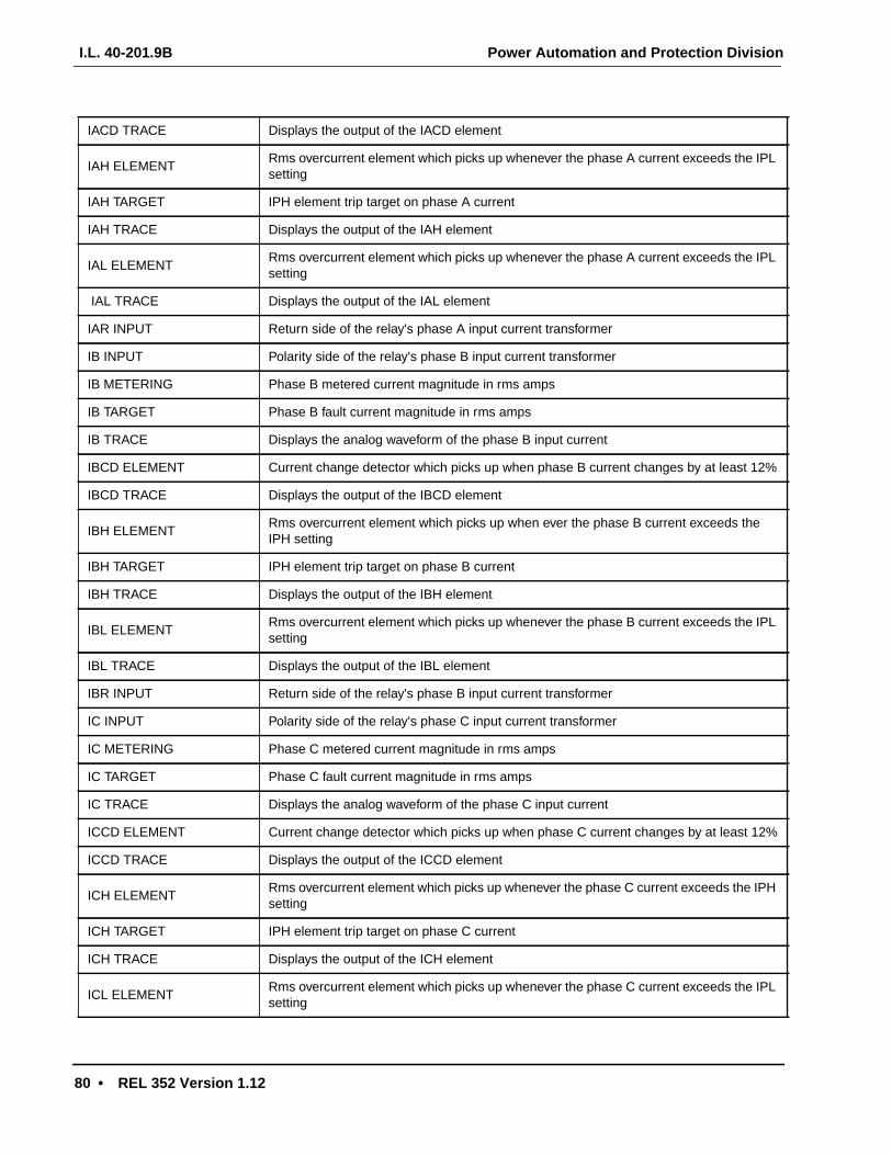
I.L. 40-201.9B Power Automation and Protection Division
80 • REL 352 Version 1.12
IACD TRACE Displays the output of the IACD element
IAH ELEMENTRms overcurrent element which picks up whenever the phase A current exceeds the IPLsetting
IAH TARGET IPH element trip target on phase A current
IAH TRACE Displays the output of the IAH element
IAL ELEMENTRms overcurrent element which picks up whenever the phase A current exceeds the IPLsetting
IAL TRACE Displays the output of the IAL element
IAR INPUT Return side of the relay's phase A input current transformer
IB INPUT Polarity side of the relay's phase B input current transformer
IB METERING Phase B metered current magnitude in rms amps
IB TARGET Phase B fault current magnitude in rms amps
IB TRACE Displays the analog waveform of the phase B input current
IBCD ELEMENT Current change detector which picks up when phase B current changes by at least 12%
IBCD TRACE Displays the output of the IBCD element
IBH ELEMENTRms overcurrent element which picks up when ever the phase B current exceeds theIPH setting
IBH TARGET IPH element trip target on phase B current
IBH TRACE Displays the output of the IBH element
IBL ELEMENTRms overcurrent element which picks up whenever the phase B current exceeds the IPLsetting
IBL TRACE Displays the output of the IBL element
IBR INPUT Return side of the relay's phase B input current transformer
IC INPUT Polarity side of the relay's phase C input current transformer
IC METERING Phase C metered current magnitude in rms amps
IC TARGET Phase C fault current magnitude in rms amps
IC TRACE Displays the analog waveform of the phase C input current
ICCD ELEMENT Current change detector which picks up when phase C current changes by at least 12%
ICCD TRACE Displays the output of the ICCD element
ICH ELEMENTRms overcurrent element which picks up whenever the phase C current exceeds the IPHsetting
ICH TARGET IPH element trip target on phase C current
ICH TRACE Displays the output of the ICH element
ICL ELEMENTRms overcurrent element which picks up whenever the phase C current exceeds the IPLsetting

Power Automation and Protection Division
REL 352 Version 1.12 • 81
GLOSSARY
ICL TRACE Displays The output of the ICL element
ICR INPUT Return side of the relay's phase C input current transformer
IGCD ELEMENT Current change detector which picks up when 3IO current changes by at least 12%
IGCD TRACE Displays the output of the IGCD element
IGH ELEMENTOperates whenever the 3IO of the input phase current exceeds the IGL setting in rmsamps
IGH TARGET IGH element trip target on 3IO current
IGH TRACE Displays the output of the IGH element
IGL ELEMENTOperates whenever the 3IO of the input phase current exceeds the IGL setting in rmsamps
IGL SETTING The IGL threshold setting in rms amps used by the IGL element
IGL TRACE Displays the output of the IGL element
IH ELEMENT The logical or of the IAH, IBH, ICH and IGH elements
IH TRACE Displays the output of the IH element
IKEY ELEMENT Operates whenever the instantaneous IT current is greater than the IKEY setting
IKEY SETTING Positive instantaneous threshold for use by the IKEY element
IKEY SIGNAL The output of the IKEY element
IKEY TRACE Displays the IKEY signal
IKO SIGNALA 75ms positive pulse which is triggered by the PT signal. Used for trip squelch keyinglogic
IKO TRACE Displays the IKO pulse
IOM ELEMENT Operates whenever the 3IO current exceeds the IOM setting in rms amps (optional)
IOM SETTING The IOM threshold setting in rms amps used by the IOM element (optional)
IOM TRACE Displays the output of the IOM element (optional)
IPH ELEMENT Picks up whenever any of the input phase currents exceeds the IPH setting in rms amps
IPH SETTING The IPH threshold setting in rms amps used by the IPH element
IPL ELEMENT Picks up whenever any of the input phase currents exceeds the IPL setting in rms amps
IPL SETTING The threshold setting in rms amps used by the IAL, IBL, and ICL elements
IT CURRENT Sequence network filter output current
IT2T SETTINGDetermines whether the 0/150 millisecond pulse stretcher will be used or not on the A2signal
ITA1 ELEMENTIt rms level detector which picks up when IT level in rms is greater than ITA1 thresholdsetting
ITA1 SETTING Threshold setting for the ITA1 element set as a percentage of the ITA2 threshold setting
ITA1 TRACE Displays the output of the ITA1 element

I.L. 40-201.9B Power Automation and Protection Division
82 • REL 352 Version 1.12
ITA2 ELEMENTIT rms level detector which picks up when IT level in rms amps is greater than ITA2setting. It’s output signal is A2
ITA2 SETTING Threshold setting in rms amps of IT current for the ITA2 element
ITA2 SIGNAL The output of the IT2T timer with A2 at it's input
ITA2 TRACE Displays the ITA2 signal
KEY OUT SIGNAL Output of the polarity logic with the IKEY signal at it's input
KEY OUT TRACE Displays the key out signal
KEY STATUS Channel transmit status = channel keyed
LDT1 ELEMENTA dual digital delay line with LP and LN as inputs and LP1 and LN1 as outputs. Timedelay determined by LDT1 setting
LDT1 SETTING Time setting in milliseconds for use by the LDT1 element
LDT1 TARGET LDT1 setting used at time of trip
LDT2 ELEMENTA dual digital delay line with LP and LN as inputs and LP2 and LN2 as outputs. Timedelay determined by LDT2 setting
LDT2 SETTING Time setting in milliseconds for use by the LDT2 element
LDT2 TARGET LDT2 setting used at time of trip
LN ELEMENT Operates whenever the instantaneous IT current is less than the (LP setting * (-1)
LN SIGNAL The output of the LN element
LN1 SIGNAL The LN signal after being delayed by the LDT1 timer
LN1 TRACE Displays the LN1 signal
LN2 SIGNAL The LN signal after being delayed by the LDT2 timer
LN2 TRACE Displays the LN2 signal
LOI ELEMENT Senses loss of current conditions (optional)
LOI STATUS Displays as YES or NO in metering mode if the backup system is activated (optional)
LOP ELEMENT Senses loss of potential conditions (optional)
LOP STATUS Displays as YES or NO in metering mode if the backup system is activated (optional)
LOP TRACE Displays status of the lop condition (optional)
LOPB SETTING Loss of potential block setting (optional)
LP ELEMENT Operates whenever the instantaneous IT current is greater than the LP setting
LP SETTINGPositive instantaneous threshold for use by the LP element, also determines negativethreshold for use by the LN element
LP SIGNAL The output of the LP element
LP TARGET Pre-fault load angle
LP1 SIGNAL The LP signal after being delayed by the LDT1 timer

Power Automation and Protection Division
REL 352 Version 1.12 • 83
GLOSSARY
LP1 TRACE Displays the LP1 signal
LP2 SIGNAL The LP signal after being delayed by the LDT2 timer
LP2 TRACE Displays the LP2 signal
M1 SIGNAL The output of the polarity circuit driven by the MARK 1 input (jumper 4)
M1 TRACE Displays the M1 signal
M2 SIGNAL The output of the polarity circuit driven by the MARK 2 input (jumper 2)
M2 TRACE Displays the M2 signal
MARK 1 INPUT The MARK 1 dc voltage input from receiver 1
MARK 2 INPUT The MARK 2 dc voltage input from receiver 2 (when used)
MIN SETTING Internal real time clock setting for minute
MNTH SETTING Internal real time clock setting for month
MPF TRACEMultiphase fault. Operates whenever the phase selector element determines fault type tomultiphase
MSEC TARGET Time of fault (milliseconds)
NPT SIGNAL Non-pilot trip generated during all trip outputs except for pilot trips
OSB TRACE Displays out-of-step blocking occurrence (optional)
OSC SETTING Oscillographic recording trigger setting
OSOT Out-of-step trip override timer setting in cycles (optional)
OST SETTING Out-of-step trip logic enable setting (optional)
OST TARGET Out-of-step trip target (optional)
OST TRACE Displays out-of-step trip occurrence (optional)
OST1 SETTING Out-of-step block timer setting in cycles (optional)
OST2 SETTING Out-of-step trip on the way in timer setting in cycles (optional)
OST3 SETTING Out-of-step trip on the way out timer setting in cycles (optional)
PANG SETTING Positive sequence line impedance angle setting in degrees
PFLC TARGET Pre-fault load current target in rms amps
PFLV TARGET Pre-fault load voltage target in rms volts
PHASE SELECTORELEMENT
A logical element which analyzes the fault currents to determine fault type
PLC Abbreviation for power line carrier equipment
PLT TARGET Pilot tripped (phase comparison trip)
PLT TRACE Displays the PLT signal
PSE SIGNALTHE power supply enable signal which is a logical 1 whenever either of the power sup-plies is energized and in good working order
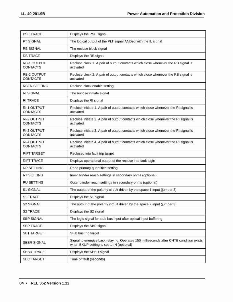
I.L. 40-201.9B Power Automation and Protection Division
84 • REL 352 Version 1.12
PSE TRACE Displays the PSE signal
PT SIGNAL The logical output of the PLT signal ANDed with the IL signal
RB SIGNAL The reclose block signal
RB TRACE Displays the RB signal
RB-1 OUTPUTCONTACTS
Reclose block 1. A pair of output contacts which close whenever the RB signal isactivated
RB-2 OUTPUTCONTACTS
Reclose block 2. A pair of output contacts which close whenever the RB signal isactivated
RBEN SETTING Reclose block enable setting
RI SIGNAL The reclose initiate signal
RI TRACE Displays the RI signal
RI-1 OUTPUTCONTACTS
Reclose initiate 1. A pair of output contacts which close whenever the RI signal isactivated
RI-2 OUTPUTCONTACTS
Reclose initiate 2. A pair of output contacts which close whenever the RI signal isactivated
RI-3 OUTPUTCONTACTS
Reclose initiate 3. A pair of output contacts which close whenever the RI signal isactivated
RI-4 OUTPUTCONTACTS
Reclose initiate 4. A pair of output contacts which close whenever the RI signal isactivated
RIFT TARGET Reclosed into fault trip target
RIFT TRACE Displays operational output of the reclose into fault logic
RP SETTING Read primary quantities setting
RT SETTING Inner blinder reach settings in secondary ohms (optional)
RU SETTING Outer blinder reach settings in secondary ohms (optional)
S1 SIGNAL The output of the polarity circuit driven by the space 1 input (jumper 5)
S1 TRACE Displays the S1 signal
S2 SIGNAL The output of the polarity circuit driven by the space 2 input (jumper 3)
S2 TRACE Displays the S2 signal
SBP SIGNAL The logic signal for stub bus input after optical input buffering
SBP TRACE Displays the SBP signal
SBT TARGET Stub bus trip target
SEBR SIGNALSignal to energize back relaying. Operates 150 milliseconds after CHTB condition existswhen BKUP setting is set to IN (optional)
SEBR TRACE Displays the SEBR signal
SEC TARGET Time of fault (seconds)

Power Automation and Protection Division
REL 352 Version 1.12 • 85
GLOSSARY
SEQUENCE NETWORKFILTER ELEMENT
Outputs a combined sequence filter current, IT. Function is determined by input currentsand coefficient settings
SET STATUS Settings access status. Can be local, remote, or both
SETR SETTING Permit setting changes to be made (remote) through communications port
SFD1 SETTING Select fault detector 1 setting. Determines carrier starter for ON/OFF applications
SFD2 SETTING Select fault detector 2 setting. Enables coincidence timing, thus trip supervision
SPACE 1 INPUT The space 1 dc voltage input from receiver 1
SPACE 2 INPUT The space 2 dc voltage input from receiver 2 (when used)
STUB BUS INPUT The dc voltage input into the relay which enables the stub bus protection when energized
T2G SETTING Trip timer setting in seconds for Z2G element (optional)
T2P SETTING Trip timer setting in seconds for the Z2P element (optional)
T3G SETTING Trip timer setting in seconds for Z3G element (optional)
T3P SETTING Trip timer setting in seconds for the Z3P element (optional)
TARGET RESET INPUT The dc voltage input into the relay which when energized causes reset of all target data
TARGET RESET SIGNAL The logic signal for target reset input after optical input buffering
TARGET RESET TRACE Displays the target reset signal
TERM SETTINGSet per 2 terminal or 3 terminal applicationsNote: For 2 or 3 terminal ON/OFF PLC applications, set TERM = 2
TEST SIGNALEnables continuous keying on a COMM = 2 scheme when relay is put into test screen oftest mode
TG TARGET Time overcurrent ground trip from optional backup distance system (optional)
TIME SETTING Enable setting of the internal real time clock
TIME STATUS Current time (hours/minutes)
TIME TARGET Time of fault (hours.minutes)
TOG ELEMENTTime ground overcurrent element which operates if the IOM element remains picked upfor a time longer than the TOG setting (optional)
TOG SETTING The time settings in seconds used by the tog element (optional)
TOG TRACE Displays the output of the TOG (TG) element (optional)
TRGG SETTING Ground current threshold setting for FDAT and OSC use
TRGP SETTING Phase current threshold setting for FDAT and OSC use
TRIP ALARM 1 OUTPUTCONTACTS
A pair of output contact which close once any trip output occurs and remains on for 5seconds after the trip contacts have opened
TRIP ALARM 2 OUTPUTCONTACTS
A pair of output contact which close once any trip output occurs and remains on for 5seconds after the trip contacts have opened
TRIP BKR-1 OUTPUTCONTACTS
Trip breaker 1 output contacts. Close whenever a trip signal is activated

I.L. 40-201.9B Power Automation and Protection Division
86 • REL 352 Version 1.12
TRIP BKR-2 OUTPUTCONTACTS
Trip breaker 2 output contacts. Close whenever a trip signal is activated
TRIP BKR-3 OUTPUTCONTACTS
Trip breaker 3 output contacts. Close whenever a trip signal is activated (optional)
TRIP BKR-4 OUTPUTCONTACTS
Trip breaker 4 output contacts. Close whenever a trip signal is activated (optional)
TRIP BKR-5 OUTPUTCONTACTS
Trip breaker 5 output contacts. Close whenever a trip signal is activated (optional)
TRIP BKR-6 OUTPUTCONTACTS
Trip breaker 6 output contacts. Close whenever a trip signal is activated (optional)
TRSL TRACE Displays operation of the trip seal-in function
UNBK SETTING Unblock trip logic enable setting
UNBK TARGET Unblock trip target
UNBK TRACE Displays operational output of the unblock trip logic
VA INPUT Polarity side of the relay's phase A input potential transformer
VA METERING phase A metered voltage magnitude in rms volts
VA TRACE Displays the analog waveform of the phase A input voltage
VACD ELEMENT Voltage change detector which picks up when phase A voltage changes by 12%
VACD TRACE Displays the output of the VACD element
VAG TARGET phase A fault voltage magnitude in rms volts
VB INPUT Polarity side of the relay's phase B input potential transformer
VB METERING Phase B metered voltage magnitude in rms volts
VB TRACE Displays the analog waveform of the phase B input voltage
VBCD ELEMENT Voltage change detector which picks up when phase B voltage changes by at least 12%
VBCD TRACE Displays the output of the VBCD element
VBG TARGET Phase B fault voltage magnitude in rms volts
VC INPUT Polarity side of the relay's phase C input potential transformer
VC METERING Phase C metered voltage magnitude in rms volts
VC TRACE Displays the analog waveform of the phase C input voltage
VCCD ELEMENT Voltage change detector which picks up when phase C voltage changes by at least 12%
VCCD TRACE Displays the output of the VCCD element
VCG TARGET Phase C fault voltage magnitude in rms volts
VERS SETTING System software version as displayed in the settings mode. Not actually a setting
VN INPUT Return for the relay's A,B, and C phase potential transformer inputs (wye connection)
VTR SETTING Potential transformer ratio setting

Power Automation and Protection Division
REL 352 Version 1.12 • 87
GLOSSARY
WDAY SETTING Internal real time clock setting for day of week
XMTR BATTERY (+) INPUT Positive (+) dc voltage input to power the isolated output transmitter circuitry
XMTR KEY (+) OUTPUTPositive key output signal to drive the transmitter key/start on the externalcommunications equipment
XMTR KEY OUT The optoisolated transmitter keying output signal with connects to the PLC keying input
XMTR RETURN (-) Negative (-) dc voltage return for both the XMTR key output and the XMTR battery input
XPUD SETTING Ohms per unit of distance multiplier used by the fault locator element
YEAR SETTING Internal real time clock setting for year
YEAR TARGET Year of fault
Z TARGET Fault impedance magnitude in ohms
Z2G ELEMENT Zone 2 ground distance (under-impedance) element (optional)
Z2G TARGET Zone 2 ground element trip target (optional)
Z2G TRACE Displays the output of the Z2G element (optional)
Z2GF SETTING Zone 2 ground forward reach setting in secondary ohms (optional)
Z2GR SETTING Zone 2 ground reverse reach setting in secondary ohms (optional)
Z2P ELEMENT Zone 2 phase distance (under-impedance) element (optional)
Z2P SETTING Zone 2 phase forward reach setting in secondary ohms (optional)
Z2P TARGET Zone 2 phase element trip target (optional)
Z2P TRACE Displays the output of the Z2P element (optional)
Z2T TRACE Zone 2 trip trace. Displays pickup of either of the Z2P or Z2G elements (optional)
Z3G ELEMENT Zone 3 ground distance (under-impedance) element (optional)
Z3G TARGET Zone 3 ground element trip target (optional)
Z3G TRACE Displays the output of the Z3G element (optional)
Z3GF SETTING Zone 3 ground forward reach setting in secondary ohms (optional)
Z3GR SETTING Zone 3 ground reverse reach setting in secondary ohms (optional)
Z3P ELEMENT Zone 3 phase distance (under-impedance) element (optional)
Z3P SETTING Zone 3 phase forward reach setting in secondary ohms (optional)
Z3P TARGET Zone 3 phase element trip target (optional)
Z3P TRACE Displays the output of the Z3P element (optional)
Z3T TRACE Zone 3 trip trace. Displays pickup of either of the Z3P or Z3G elements (optional)
ZR SETTING Line impedance ratio setting (Z0 line / Z1 line). Used by the ground distance algorithms

I.L. 40-201.9B Power Automation and Protection Division
88 • REL 352 Version 1.12
THIS PAGE RESERVED FOR NOTES
Power Automation and Protection Division
REL 352 Version 1.12 • 89
A
BACKPLANE MODULE
Schematic - - - - - - - - - - - - - - - - - - - - - 1612C22
Component Location Diagrams - - - - - - 1611C26, 1502B38
All external electrical connections pass thru the Backplane module (see figure 4-1, page 50) of the outer chas-sis. Seven DIN connectors (J11, J12, J13, JA1, JA2, JA3 and JA4) allow for the removal of the outer chassis(Backplane module) from the inner chassis (Interconnect module, Contact Input and Relay Output modules).
Electrical inputs to the Backplane module, which are routed through the FT-14 switch to the Backplate, include:
• VA, VB, VC, and VN
• IA/IAR, IB/IBR, IC/ICR
• BP(48, 125 or 250 Vdc) and BN (common) for primary and backup power inputs.
The Backplane module, (see figure A-1 and Schematic, page 90) contains three voltage-type transformers, forVA/VN (VAN), VB/VN (VBN), VC/VN (VCN) inputs.
A Transformer module (see figure A-2 and Schematic, page 91) is piggybacked onto the Backplane module,consisting of three current-type transformers (IA, IB, IC) with three 0.1% resistors. The primary windings of allsix transformers are directly-connected to the input terminal (TB6/1 thru 10); the secondary windings are con-nected thru the Interconnect module to the Analog Input module. The current transformers (IA, IB, IC) are notgapped; dc offset attenuation is done with a digital filtering algorithm. Surge suppression is included where thesignals enter the module.
The Backplane module also includes:
• 4 chokes (L1 thru L4) for dc power supply filter
• surge-suppressor capacitors
INCOM/PONI is supplied in two versions:
• INCOM/PONI to RS232 computer interface (supplied as standard).
• INCOM/PONI to INCOM network interface (supplied as option).
I.L. 40-201.9BP
ower A
utomation and P
rotection Division
90•
RE
L 352 Version 1.12
* Denotes Change
1611C26* Sub 11
Figure A-1 REL 352 Backplane Module Component Location Diagram
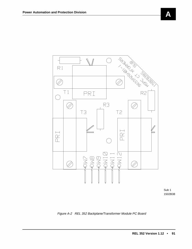
Power Automation and Protection Division
REL 352 Version 1.12 • 91
A
1502B38Sub 1
Figure A-2 REL 352 Backplane/Transformer Module PC Board
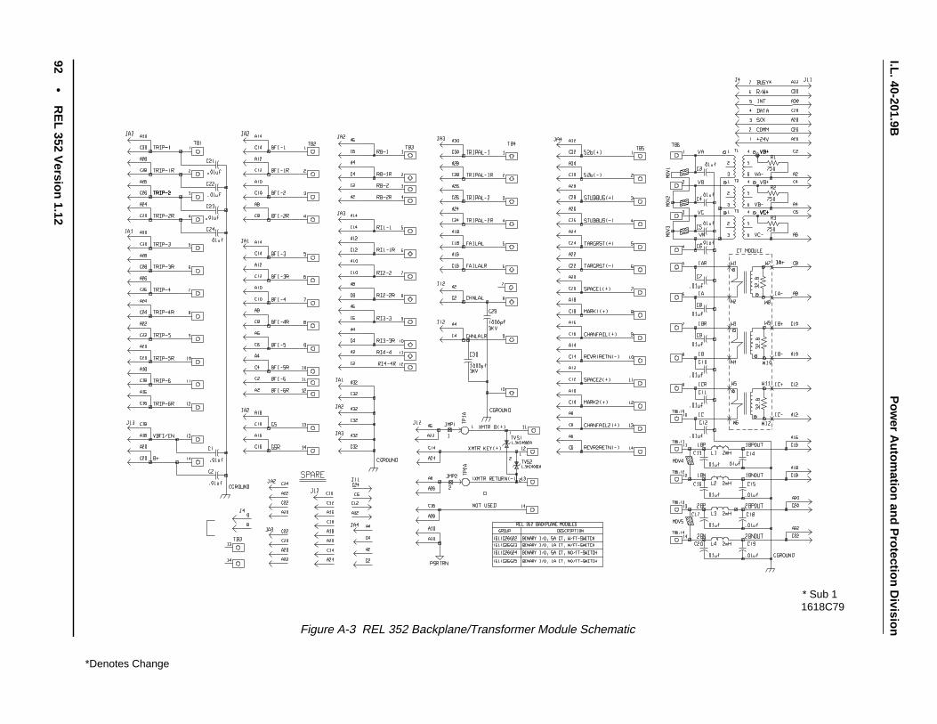
I.L. 40-201.9BP
ower A
utomation and P
rotection Division
92•
RE
L 352 Version 1.12
1618C79* Sub 1
*Denotes Change
Figure A-3 REL 352 Backplane/Transformer Module Schematic
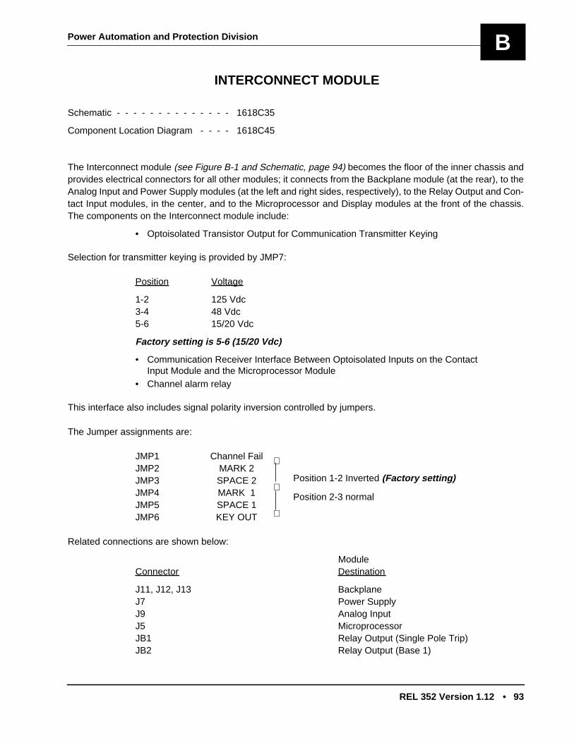
Power Automation and Protection Division
REL 352 Version 1.12 • 93
B
INTERCONNECT MODULE
Schematic - - - - - - - - - - - - - - 1618C35
Component Location Diagram - - - - 1618C45
The Interconnect module (see Figure B-1 and Schematic, page 94) becomes the floor of the inner chassis andprovides electrical connectors for all other modules; it connects from the Backplane module (at the rear), to theAnalog Input and Power Supply modules (at the left and right sides, respectively), to the Relay Output and Con-tact Input modules, in the center, and to the Microprocessor and Display modules at the front of the chassis.The components on the Interconnect module include:
• Optoisolated Transistor Output for Communication Transmitter Keying
Selection for transmitter keying is provided by JMP7:
Position Voltage
1-2 125 Vdc3-4 48 Vdc5-6 15/20 Vdc
Factory setting is 5-6 (15/20 Vdc)
• Communication Receiver Interface Between Optoisolated Inputs on the ContactInput Module and the Microprocessor Module
• Channel alarm relay
This interface also includes signal polarity inversion controlled by jumpers.
The Jumper assignments are:
JMP1 Channel FailJMP2 MARK 2JMP3 SPACE 2JMP4 MARK 1JMP5 SPACE 1JMP6 KEY OUT
Related connections are shown below:
ModuleConnector Destination
J11, J12, J13 BackplaneJ7 Power SupplyJ9 Analog InputJ5 MicroprocessorJB1 Relay Output (Single Pole Trip)JB2 Relay Output (Base 1)
Position 1-2 Inverted (Factory setting)
Position 2-3 normal

I.L. 40-201.9BP
ower A
utomation and P
rotection Division
94•
RE
L 352 Version 1.12
1618C45Sub 1
Figure B-1: REL 352 Interconnect Module Component Location Diagram
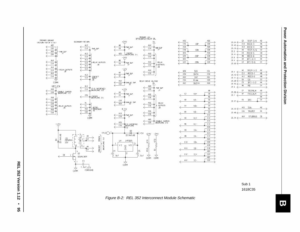
Pow
er Autom
ation and Protection D
ivision
RE
L 352 Version 1.12
•95
B
1618C35
Sub 1
Figure B-2: REL 352 Interconnect Module Schematic
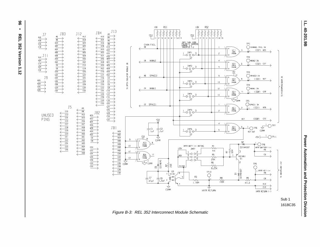
I.L. 40-201.9BP
ower A
utomation and P
rotection Division
96•
RE
L 352 Version 1.12
1618C35
Sub 1
Figure B-3: REL 352 Interconnect Module Schematic
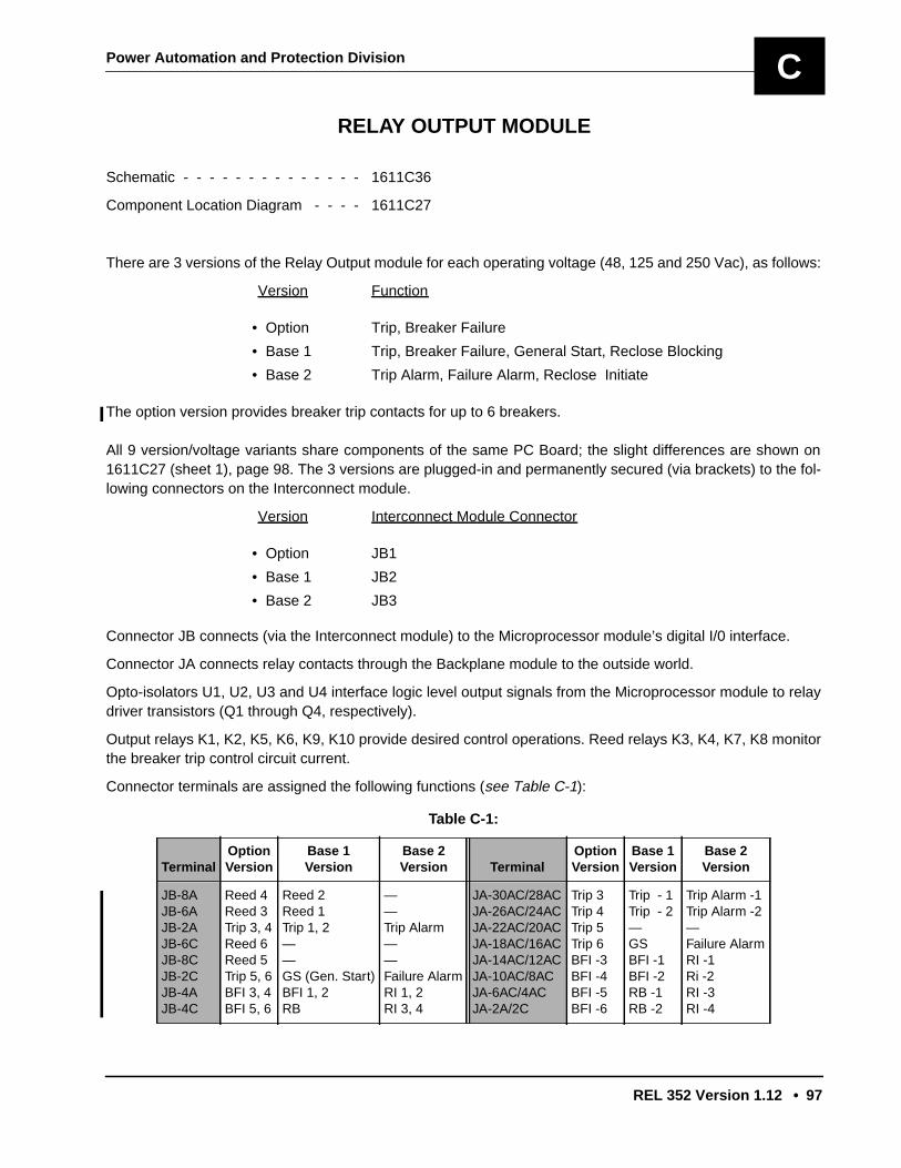
Power Automation and Protection Division
REL 352 Version 1.12 • 97
C
RELAY OUTPUT MODULE
Schematic - - - - - - - - - - - - - - 1611C36
Component Location Diagram - - - - 1611C27
There are 3 versions of the Relay Output module for each operating voltage (48, 125 and 250 Vac), as follows:
Version Function
• Option Trip, Breaker Failure
• Base 1 Trip, Breaker Failure, General Start, Reclose Blocking
• Base 2 Trip Alarm, Failure Alarm, Reclose Initiate
The option version provides breaker trip contacts for up to 6 breakers.
All 9 version/voltage variants share components of the same PC Board; the slight differences are shown on1611C27 (sheet 1), page 98. The 3 versions are plugged-in and permanently secured (via brackets) to the fol-lowing connectors on the Interconnect module.
Version Interconnect Module Connector
• Option JB1
• Base 1 JB2
• Base 2 JB3
Connector JB connects (via the Interconnect module) to the Microprocessor module’s digital I/0 interface.
Connector JA connects relay contacts through the Backplane module to the outside world.
Opto-isolators U1, U2, U3 and U4 interface logic level output signals from the Microprocessor module to relaydriver transistors (Q1 through Q4, respectively).
Output relays K1, K2, K5, K6, K9, K10 provide desired control operations. Reed relays K3, K4, K7, K8 monitorthe breaker trip control circuit current.
Connector terminals are assigned the following functions (see Table C-1):
Table C-1:
TerminalOptionVersion
Base 1Version
Base 2Version Terminal
OptionVersion
Base 1Version
Base 2Version
JB-8AJB-6AJB-2AJB-6CJB-8CJB-2CJB-4AJB-4C
Reed 4Reed 3Trip 3, 4Reed 6Reed 5Trip 5, 6BFI 3, 4BFI 5, 6
Reed 2Reed 1Trip 1, 2——GS (Gen. Start)BFI 1, 2RB
——Trip Alarm——Failure AlarmRI 1, 2RI 3, 4
JA-30AC/28ACJA-26AC/24ACJA-22AC/20ACJA-18AC/16ACJA-14AC/12ACJA-10AC/8ACJA-6AC/4ACJA-2A/2C
Trip 3Trip 4Trip 5Trip 6BFI -3BFI -4BFI -5BFI -6
Trip - 1Trip - 2—GSBFI -1BFI -2RB -1RB -2
Trip Alarm -1Trip Alarm -2—Failure AlarmRI -1Ri -2RI -3RI -4
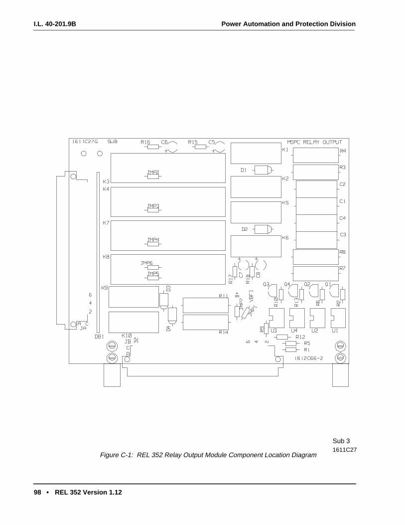
I.L. 40-201.9B Power Automation and Protection Division
98 • REL 352 Version 1.12
1611C27Sub 3
Figure C-1: REL 352 Relay Output Module Component Location Diagram
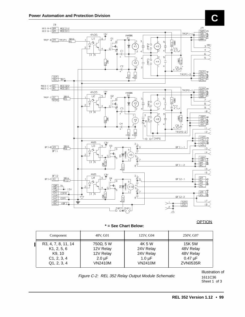
Power Automation and Protection Division
REL 352 Version 1.12 • 99
C
* = See Chart Below:
Component 48V, G01 125V, G04 250V, G07
R3, 4, 7, 8, 11, 14K1, 2, 5, 6
K9, 10C1, 2, 3, 4Q1, 2, 3, 4
750Ω, 5 W12V Relay12V Relay
2.0 µFVN2410M
4K 5 W24V Relay24V Relay
1.0 µFVN2410M
15K 5W48V Relay48V Relay
0.47 µFZVN0535R
BF
I-6
BF
I-5
BF
I-4
BF
I-3
TR
IP 6
TR
IP 5
TR
IP 4
TR
IP 3
OPTION
1611C36Illustration of
Sheet 1 of 3
Figure C-2: REL 352 Relay Output Module Schematic
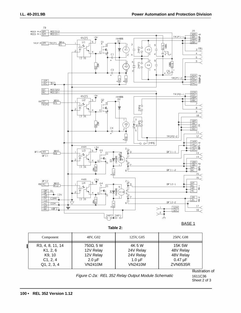
I.L. 40-201.9B Power Automation and Protection Division
100 • REL 352 Version 1.12
TR
IP-1
TR
IP-2
TR
IP-1
BF
I -1
BF
I -2
BASE 1
1611C36Illustration of
Sheet 2 of 3
Table 2:
Component 48V, G02 125V, G05 250V, G08
R3, 4, 8, 11, 14K1, 2, 6K9, 10
C1, 2, 4Q1, 2, 3, 4
750Ω, 5 W12V Relay12V Relay
2.0 µFVN2410M
4K 5 W24V Relay24V Relay
1.0 µFVN2410M
15K 5W48V Relay48V Relay
0.47 µFZVN0535R
Figure C-2a: REL 352 Relay Output Module Schematic
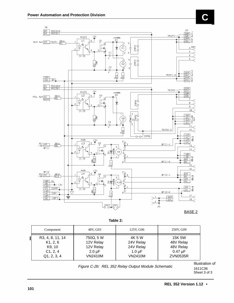
Power Automation and Protection Division
REL 352 Version 1.12 •101
C
BASE 2
RI-
1R
I-2
RI-
3R
I-4
Table 2:
Component 48V, G03 125V, G06 250V, G09
R3, 4, 8, 11, 14K1, 2, 6K9, 10
C1, 2, 4Q1, 2, 3, 4
750Ω, 5 W12V Relay12V Relay
2.0 µFVN2410M
4K 5 W24V Relay24V Relay
1.0 µFVN2410M
15K 5W48V Relay48V Relay
0.47 µFZVN0535R
1611C36Illustration of
Sheet 3 of 3
Figure C-2b: REL 352 Relay Output Module Schematic

I.L. 40-201.9B Power Automation and Protection Division
102 • REL 352 Version 1.12
THIS PAGE RESERVED FOR NOTES

Power Automation and Protection Division
REL 352 Version 1.12 • 103
D
OPTOISOLATED INPUT MODULE
Schematic - - - - - - - - - - - - - - - - - - - - - 1618C36 (2 sheets)
Component Location Diagram - - - - - - - 1618C38
1. THE OPTOISOLATED INPUT MODULE PROVIDES OPTO-ISOLATED INPUT INTERFACES FROM:
Optoisolated Inputs
Optoisolated Inputs 52b, STUB Bus, Target Reset to logic level inputs on the Microprocessor module. This partcontains 3 identical circuits, jumper positions JMP7 to JMP9.
(1-2) are for 15/20 Vdc(3-4) are for 48/125 Vdc(5-6) are for 220/250 Vdc
Note: Position 3-4 is the factory setting.
Receiver Inputs
These inputs (SPACE 1, MARK 1, CHAN FAIL 1, SPACE 2, MARK 2, CHAN FAIL 2) interface to an externalcommunication receiver such as Power Line Carrier, Audio Tone, etc.
Jumper Positions JMP1 to JMP6:1-2 are for 15/20 Vdc7-8 are for 48 Vdc9-10 are for 125 Vdc
Note: Position 1-2 is the factory setting.
• Connector JA connects to the Backplane module and, via terminal block TB-5, to the exter-nal contacts.
• Connector JB interfaces to the Microprocessor module via connector JB-4 (on the intercon-nect module).
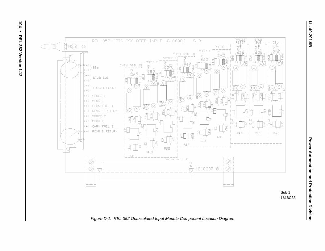
I.L. 40-201.9BP
ower A
utomation and P
rotection Division
104•
RE
L 352 Version 1.12
1618C38Sub 1
Figure D-1: REL 352 Optoisolated Input Module Component Location Diagram
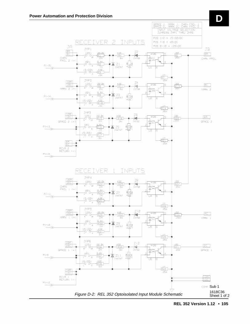
Power Automation and Protection Division
REL 352 Version 1.12 • 105
D
1618C36Sub 1
Sheet 1 of 2Figure D-2: REL 352 Optoisolated Input Module Schematic
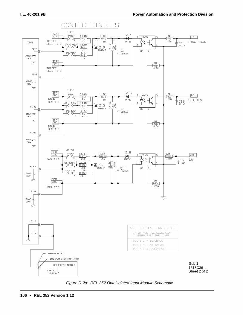
I.L. 40-201.9B Power Automation and Protection Division
106 • REL 352 Version 1.12
1618C36Sub 1
Sheet 2 of 2
Figure D-2a: REL 352 Optoisolated Input Module Schematic
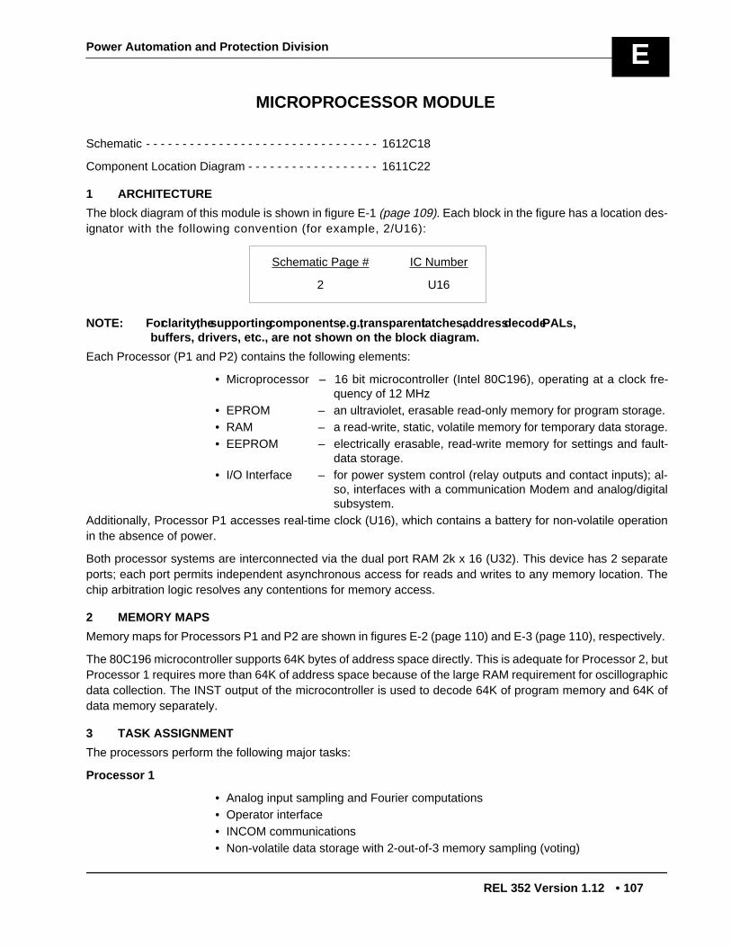
Power Automation and Protection Division
REL 352 Version 1.12 • 107
E
MICROPROCESSOR MODULE
Schematic - - - - - - - - - - - - - - - - - - - - - - - - - - - - - - - - 1612C18
Component Location Diagram - - - - - - - - - - - - - - - - - - 1611C22
1 ARCHITECTURE
The block diagram of this module is shown in figure E-1
(page 109)
. Each block in the figure has a location des-ignator with the following convention (for example, 2/U16):
NOTE: For clarity, the supporting components, e.g., transparent latches, address decode PALs,buffers, drivers, etc., are not shown on the block diagram.
Each Processor (P1 and P2) contains the following elements:
• Microprocessor – 16 bit microcontroller (Intel 80C196), operating at a clock fre-quency of 12 MHz
• EPROM – an ultraviolet, erasable read-only memory for program storage.• RAM – a read-write, static, volatile memory for temporary data storage.• EEPROM – electrically erasable, read-write memory for settings and fault-
data storage.• I/O Interface – for power system control (relay outputs and contact inputs); al-
so, interfaces with a communication Modem and analog/digitalsubsystem.
Additionally, Processor P1 accesses real-time clock (U16), which contains a battery for non-volatile operationin the absence of power.
Both processor systems are interconnected via the dual port RAM 2k x 16 (U32). This device has 2 separateports; each port permits independent asynchronous access for reads and writes to any memory location. Thechip arbitration logic resolves any contentions for memory access.
2 MEMORY MAPS
Memory maps for Processors P1 and P2 are shown in figures E-2 (page 110) and E-3 (page 110), respectively.
The 80C196 microcontroller supports 64K bytes of address space directly. This is adequate for Processor 2, butProcessor 1 requires more than 64K of address space because of the large RAM requirement for oscillographicdata collection. The INST output of the microcontroller is used to decode 64K of program memory and 64K ofdata memory separately.
3 TASK ASSIGNMENT
The processors perform the following major tasks:
Processor 1
• Analog input sampling and Fourier computations• Operator interface• INCOM communications• Non-volatile data storage with 2-out-of-3 memory sampling (voting)
Schematic Page # IC Number
2 U16
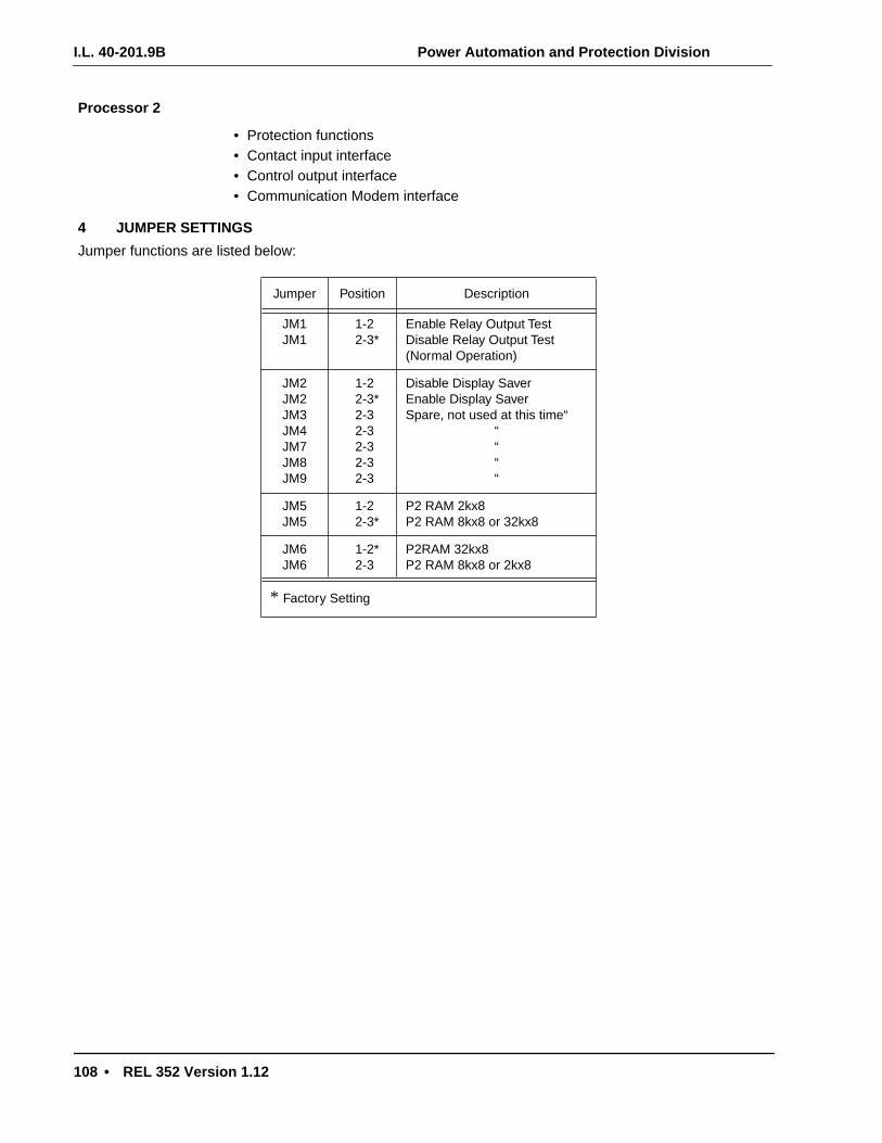
I.L. 40-201.9B Power Automation and Protection Division
108 • REL 352 Version 1.12
Processor 2
• Protection functions• Contact input interface• Control output interface• Communication Modem interface
4 JUMPER SETTINGS
Jumper functions are listed below:
Jumper Position Description
JM1JM1
1-22-3*
Enable Relay Output TestDisable Relay Output Test(Normal Operation)
JM2JM2JM3JM4JM7JM8JM9
1-2 2-3*2-3 2-3 2-3 2-3 2-3
Disable Display SaverEnable Display SaverSpare, not used at this time“
““““
JM5JM5
1-22-3*
P2 RAM 2kx8P2 RAM 8kx8 or 32kx8
JM6JM6
1-2*2-3
P2RAM 32kx8P2 RAM 8kx8 or 2kx8
*
Factory Setting
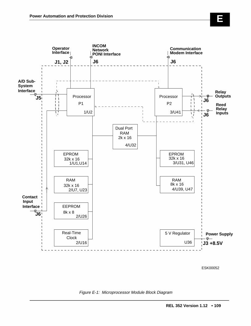
Power Automation and Protection Division
REL 352 Version 1.12 • 109
E
Processor Processor
P1 P2
1/U2 3/U41
Dual Port RAM
2k x 16
4/U32
EPROM
RAM
EEPROM
Real-TimeClock
5 V Regulator
RAM
EPROM32k x 16
32k x 16
8k x 8
2/U16
2/U26
2/U7, U23
1/U1,U14 3/U31, U46
4/U39, U47
U36
φ
φ
φ
φ
φ
φ
φ φ φ
Relay
Reed
J6
J6
J3 +8.5V
Power Supply
CommunicationModem Interface
J6
INCOM NetworkPONI Interface
OperatorInterface
J6J1, J2
A/D Sub-
Interface
J5
Contact
Interface
J6
System
Input
32k x 16
8k x 16
ESK00052
Outputs
RelayInputs
Figure E-1: Microprocessor Module Block Diagram

I.L. 40-201.9B Power Automation and Protection Division
110 • REL 352 Version 1.12
4k Memory Mapped I/0
4k Dual Port RAM (2k x 16)
8k DB2 8k DB5(4k x 16) (4k x 16)
8k DB1 8k DB4(4k x 16) (4k x 16)
8k DB0 8k DB3(4k x 16) (4k x 16)
8k Permanent RAM (4k x 16)
8k EEPROM (8k x 8)
64k EPROM Program Memory(32k x 16)
80C196 special Function Registers
FFFFH
F000H
E000H
C000H
A000H
8000H
6000H
4000H
100H
0H
DA
TA
ME
MO
RY
ESK00053
Memory Mapped I/0
Dual Port RAM(2k x 16)
RAM
(4k x 16)
Program Memory (EPROM)
80C196 InternalRegister File
FFFFH
F000H
E000H
C000H
100H
0H
4k
4k
8k
48k
ESK00054
Figure E-2: REL 352 Processor 1 Memory Map
Figure E-3: REL 352 Processor 2 Memory Map
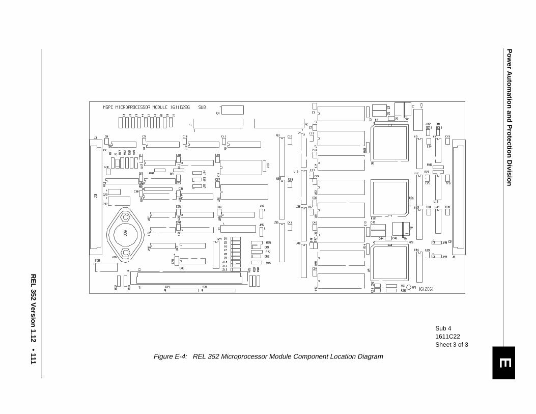
P
ower A
utomation and P
rotection Division
RE
L 352 Version 1.12
•111
E
Figure E-4: REL 352 Microprocessor Module Component Location Diagram
Sub 41611C22Sheet 3 of 3

I.L. 40-201.9B Power Automation and Protection Division
112 • REL 352 Version 1.12
Figure E-5: REL 352 Microprocessor Module Schematic (sheet 1 of 7)
Sub 11612C18-352
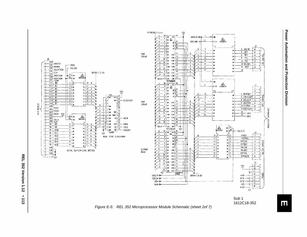
Po
wer A
uto
matio
n an
d P
rotectio
n D
ivision
RE
L 352 V
ersion
1.12•
113 E
Figure E-5: REL 352 Microprocessor Module Schematic (sheet 2of 7)
Sub 11612C18-352
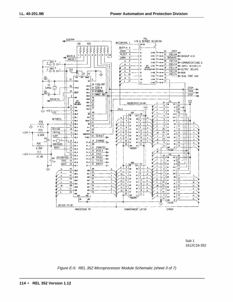
I.L. 40-201.9B Power Automation and Protection Division
114 • REL 352 Version 1.12
Figure E-5: REL 352 Microprocessor Module Schematic (sheet 3 of 7)
Sub 11612C18-352
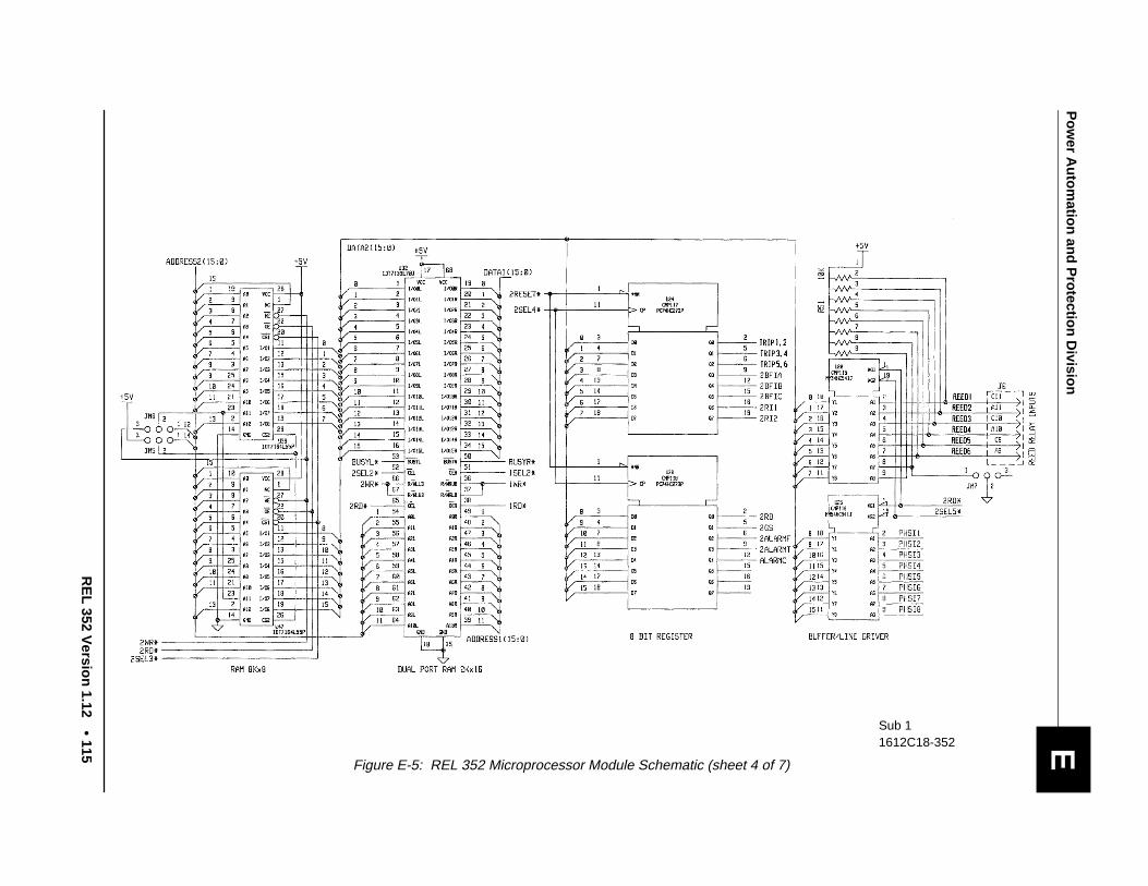
Po
wer A
uto
matio
n an
d P
rotectio
n D
ivision
RE
L 352 V
ersion
1.12•
115 E
Figure E-5: REL 352 Microprocessor Module Schematic (sheet 4 of 7)
Sub 11612C18-352

I.L. 40-201.9B
Po
wer A
uto
matio
n an
d P
rotectio
n D
ivision
116•
RE
L 352 V
ersion
1.12
Figure E-5: REL 352 Microprocessor Module Schematic (sheet 5 of 7)
Sub 11612C18-352

Po
wer A
uto
matio
n an
d P
rotectio
n D
ivision
RE
L 352 V
ersion
1.12•
117 E
Figure E-5: REL 352 Microprocessor Module Schematc (sheet 6 of 7)
Sub 11612C18-352
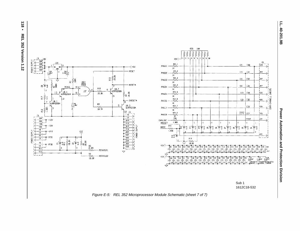
I.L. 40-201.9B
Po
wer A
uto
matio
n an
d P
rotectio
n D
ivision
118•
RE
L 352 V
ersion
1.12
Figure E-5: REL 352 Microprocessor Module Schematic (sheet 7 of 7)
Sub 11612C18-532

Power Automation and Protection Division
REL 352 Version 1.12 • 119
E
Table E-1. Communication Interface Inputs to Microprocessor Board
J6 Pin Signal Name Destination Function
28c ID0 U25-2 MARK 1
28a ID1 U25-3 SPACE 1
27c ID2 U25-4 MARK 2
27a ID3 U25-5 SPACE 2
26c ID4 U25-6 Not used
26a ID5 U25-7 Not used
25c ID6 U25-8 Not used
25a ID7 U25-9 ECF *
24c PINT U41-24 (HSI0) Not used
24a MRESET U41-15 (EXTINT) Not used
18a RECCHL U41-10 (P0.5) Not used
18c TXMCHL U41-8 (P0.6) Not used
NOTE: * Low True Signal
Table E-2. O
utputs From Microprocessor To Communication Interface
J6 Pin Signal Name Destination Function
23c OD0 U38-2 XMTR KEY
23a OD1 U38-5 Not used
22c OD2 U38-6 Not used
22a OD3 U38-9 Not used
21c OD4 U38-12 Not used
21a OD5 U38-15 Not used
20c OD6 U38-16 Not used
20a OD7 U38-19 Not used
19c OC0 U29-12 Not used
17c OC1 U29-15 Not used
19a DATAVAL U35-21 Not used

I.L. 40-201.9B Power Automation and Protection Division
120 • REL 352 Version 1.12
THIS PAGE RESERVED FOR NOTES
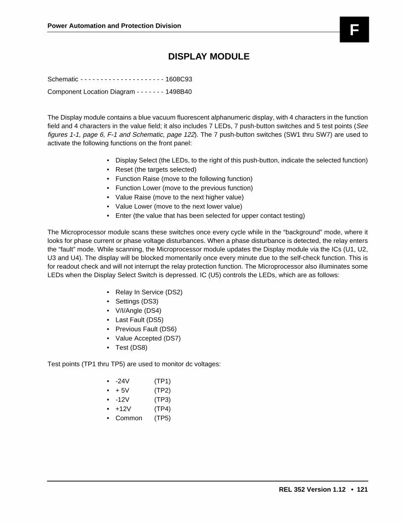
Power Automation and Protection Division
REL 352 Version 1.12 • 121
F
DISPLAY MODULE
Schematic - - - - - - - - - - - - - - - - - - - - - 1608C93
Component Location Diagram - - - - - - - 1498B40
The Display module contains a blue vacuum fluorescent alphanumeric display, with 4 characters in the functionfield and 4 characters in the value field; it also includes 7 LEDs, 7 push-button switches and 5 test points (Seefigures 1-1, page 6, F-1 and Schematic, page 122). The 7 push-button switches (SW1 thru SW7) are used toactivate the following functions on the front panel:
• Display Select (the LEDs, to the right of this push-button, indicate the selected function)• Reset (the targets selected)• Function Raise (move to the following function)• Function Lower (move to the previous function)• Value Raise (move to the next higher value)• Value Lower (move to the next lower value)• Enter (the value that has been selected for upper contact testing)
The Microprocessor module scans these switches once every cycle while in the “background” mode, where itlooks for phase current or phase voltage disturbances. When a phase disturbance is detected, the relay entersthe “fault” mode. While scanning, the Microprocessor module updates the Display module via the ICs (U1, U2,U3 and U4). The display will be blocked momentarily once every minute due to the self-check function. This isfor readout check and will not interrupt the relay protection function. The Microprocessor also illuminates someLEDs when the Display Select Switch is depressed. IC (U5) controls the LEDs, which are as follows:
• Relay In Service (DS2)• Settings (DS3)• V/I/Angle (DS4)• Last Fault (DS5)• Previous Fault (DS6)• Value Accepted (DS7)• Test (DS8)
Test points (TP1 thru TP5) are used to monitor dc voltages:
• -24V (TP1)• + 5V (TP2)• -12V (TP3)• +12V (TP4)• Common (TP5)

I.L. 40-201.9BP
ower A
utomation and P
rotection Division
122•
RE
L 352 Version 1.12
1498B40Sub 4
Sheet 7 of 7
Figure F-1: REL 352 Display Module Component Location Diagram
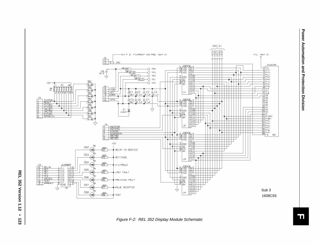
Pow
er Autom
ation and Protection D
ivision
RE
L 352 Version 1.12
•123
F
1608C93
Sub 3
Figure F-2: REL 352 Display Module Schematic

I.L. 40-201.9B Power Automation and Protection Division
124 • REL 352 Version 1.12
THIS PAGE RESERVED FOR NOTES

Power Automation and Protection Division
REL 352 Version 1.12 • 125
G
POWER SUPPLY MODULE
Schematic - - - - - - - - - - - - - - - - - - - - - 1356D56
Component Location Diagram - - - - - - - 1611C24
The Power Supply Module consists of two identical power supplies whose outputs are auctioneered throughdiodes to provide an uninterrupted power source, in the event one of the supplies fails. The following descriptionis provided for one supply (both supplies are identical).
The input power from terminals J7/26AC and 28AC is applied to fuses F1 and F2, rectifier bridge BR1 and filternetwork R1, C1. Therefore, both dc and ac operation are possible.
Switching transistor Q2 is turned on and off to provide current for the flywheel inductors L1 and L2 which feed
the charge capacitor C11. When transistor Q2 is turned off, the flywheel current continues through diode D5.
The dc voltage, developed across C11, is applied through resistor divider R7, R17 and R14 to the pulse widthmodulator U1, pin 1. In U1, this voltage is compared with the voltage on pin 2, which is derived from an internalZener reference voltage on pin 16. The voltage difference between pins 1 and 2 controls the high or low dutycycle (or pulse width) of the ac waveform on pins 12 and 13. The frequency of this ac signal is determined byR13 and C7. This ac signal is amplified by transistor Q4 which controls the gate of switching transistor Q2 thrudriver Q3; thus completing the feedback loop which controls the voltage on capacitor C11.
Chip U1 is powered from internal element VC1 (12 volt). On powerup, VC1, is initially generated from voltageacross Zener diode Z2, driving the emitter follower Q1. VC1 also initially powers transistors Q3 and Q4 thru di-ode D1. When the voltage across C11 gradually builds up, and overtakes VC1, transistors Q3 and Q4 will bepowered through R16 and D2. When the voltage across C11 reaches about 75% of its final value, the currentthrough R3 will back bias Q1 through diode D4, turning off Q1 and supplying VC1 through R3 from the voltageacross C11. This arrangement minimizes the power dissipation on Q1. For the same reason, it is extremely im-portant to limit the current from P12V (Terminal J7 14AC) to 10mA. Otherwise, the turn off of Q1 may be ham-pered, and serious overheating will result. The gradual buildup of voltage across C11 is controlled by capacitorC3.
Overload protection is provided by sense resistors R18, R19 and R20 through filter R5 and C6 to control input(pin 5) of chip, U1.
The primary dc voltage (PRDC 1) across C11 is converted to a regulated ac voltage, with the aid of U2 and U3devices that alternately control switching transistors Q5 and Q6, thereby providing power to the primary windingof transformer T1. Protection against accidental shorts is provided by sensing resistors R28, R29 and R30,through filter R27 and C12, to control pin 4 of U2.
The secondary winding of transformer T1, on terminals 6, 7 and 10 provides:
• +12 Vdc thru full wave rectifier D17 and D18 and auctioneering diode D21 (to termi-nal J2/28A, 28C)
• -12 Vdc thru full wave rectifier D15 and D11 and auctioneering diode D14 (to terminalJ2/30A, 30C)
• +24 Vdc thru voltage doubler circuit C16, C19, D23, C18 and auctioneering diodeD24 (to terminal J7/8A, 8C)
• -24 Vdc thru voltage doubler circuit C17, D20, D25, C19 and auctioneering diodeD22 (to terminal J7/6A, 6C)

I.L. 40-201.9B Power Automation and Protection Division
126 • REL 352 Version 1.12
The secondary winding of transformer T1, on terminals 8 and 9 provides:
• +8.5 Vdc thru full wave bridge rectifier D10, D11, D12, D13 and auctioneering diodeD9 (to terminal J2/20A, 20C, 22A and 22C) (also to terminal J7/10A, 10C)
The secondary winding of transformer T1, on terminals 4 and 5 provides:
• 6.5 Vac for the electroluminescent display (to terminals J2/4A, 4C and 6A, 6C)
The 6.5 Vac is switched by relay K1, since it is impossible to auctioneer two nonsynchronized ac voltages. RelayK1 is controlled by status monitor U7. The 6.5 Vac output is biased at -20 Vdc to satisfy the requirements of theelectroluminescent display.
The status monitor U7 checks the health of each power supply by monitoring the +8.5 Vdc outputs of each sup-ply. The status outputs are normally low, thus, a high output means a failed power supply (Terminal J2/12A,12C).
Each power supply is capable of delivering a total output of 35 W power, distributed among its six load outputs.
Due to the maximum diode rating of 1A, no individual load should exceed a current drain of 1A.
ADJUSTMENTS
To achieve optimum performance, the following adjustments are required:
Adjust Power Supply To Achieve On Comments
R17 1 26.00Vdc PRDC1 (Term. J7/16AC) G01R17 1 70.00Vdc PRDC1 (Term. J7/16AC) G02 and G03R50 2 26.00Vdc PRDC2 (Term. J7/18AC) G01R50 2 70.00Vdc PRDC2 (Term. J7/18AC) G02 and G03
NOTE: For proper operation of the auctioneered outputs, PRDC1 and PRDC2 shouldhave identical values.
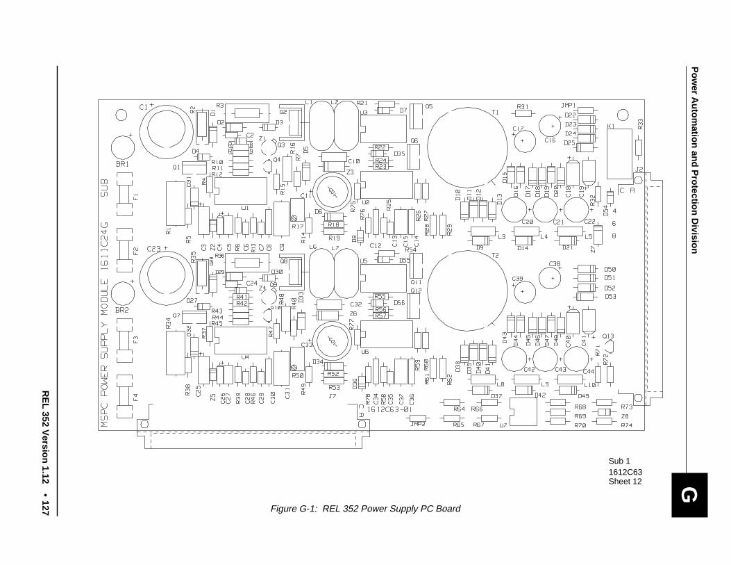
Pow
er Autom
ation and Protection D
ivision
RE
L 352 Version 1.12
•127
G
Figure G-1: REL 352 Power Supply PC Board
Sub 11612C63Sheet 12

I.L. 40-201.9B Power Automation and Protection Division
128 • REL 352 Version 1.12
*Sub 61356D56
SEE INSIDE
FOR FOLD OUT BACK COVER
DRAWING
Figure G-2: REL 352 Power Supply Schematic
*Denotes Change

Power Automation and Protection Division
REL 352 Version 1.12 129
H
ANALOG INPUT MODULE
Schematic - - - - - - - - - - - - - - - - - - - - - - - - - - - - - - - - 1612C20
Component Location diagram - - - - - - - - - - - - - - - - - - 1611C23
The block diagram of this module is shown in figure H-1 (page 130). The module interfaces with the voltage andcurrent transformers that are mounted on the Backplane module. These transformers provide the following acvalues: VA, VB, VC, IA, IB, IC. The values are applied to active third-order Butterworth antialiasing filters (U8 thru
U13), with a cut-off frequency determined by the Nyquist criterion and the system sampling rate. Values IA, IB,
IC are summed to produce 3I0 in U5. All seven values (VA, VB, VC, IA, IB, IC, 3I0) are applied to the multiplexer
(U5), whose output connects to the A/D converter (U15) via autoranging circuitry.
The A/D converter is a 12 bit plus sign with an internal sample-and-hold amplifier. Additionally, on request, theA/D converter executes a self-calibrating routine that corrects zero errors and, also, full-scale and linearity er-rors. Device U16 provides stable, precision 5.000 V reference to the A/D converter. The autoranging circuitryprovides 16 bits of dynamic range needed to measure high current values during power system faults.
The 13 bit output is available from the A/D converter (12 bit plus sign). To achieve a 16-bit range requires amultiplication of the A/D converter output (or gain) by eight.
If the input value satisfies the expression:
+ 0.5 V < VIN < - 0.5 V
then the comparators (U3.1 and U3.2) select the Y0 - Y) switch of U4, and multiplication by 8 takes place in the
Microprocessor software.
For the range:
- 0.5 V < IIN < + 0.5 V
the (Y1 - Y) path of U4 is selected (by U3.1 and U3.2), connecting the output of U2 (analog input with a gain of
8) to the A/D converter, performing a multiplication by 8 in the analog domain.
NOTE: Adjust potentiometer (R59) for 5.000V at the test point (TP2) to ground.
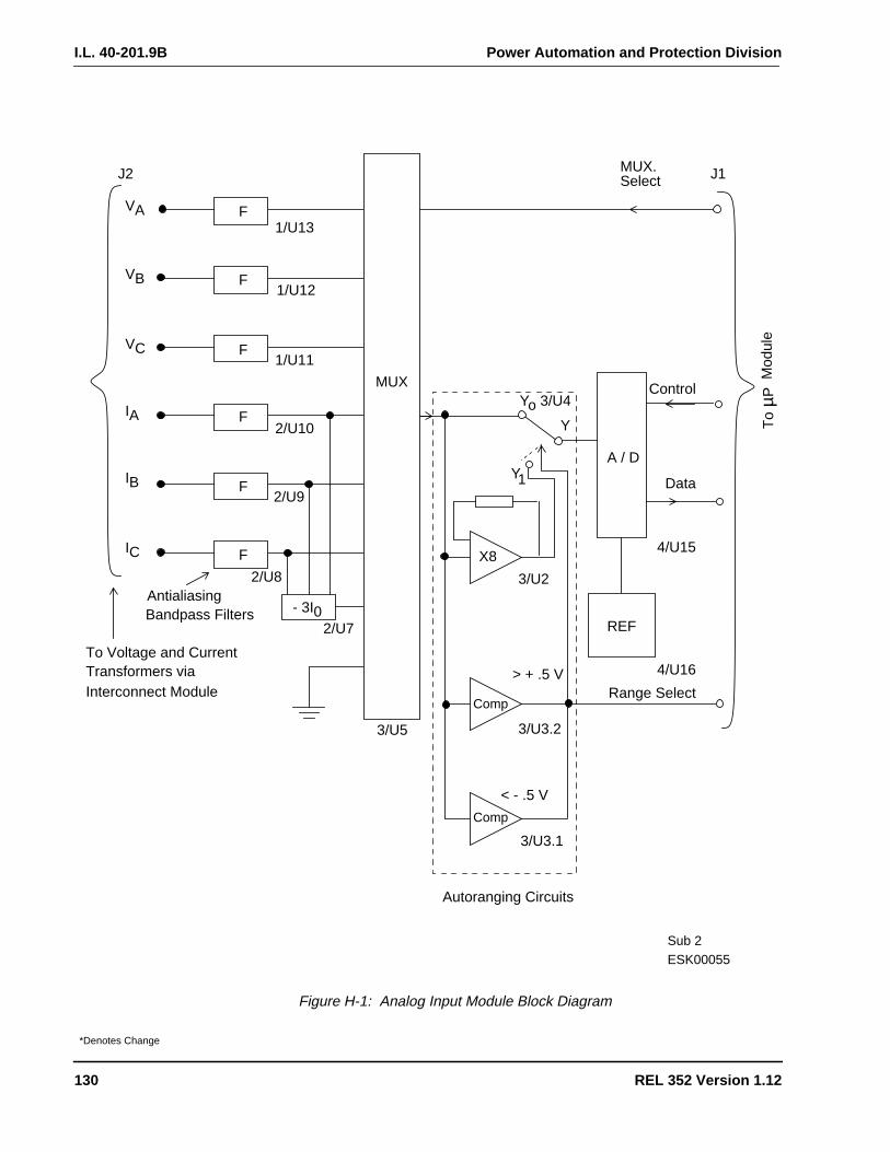
I.L. 40-201.9B Power Automation and Protection Division
130 REL 352 Version 1.12
VA
VB
VC
IA
IB
IC
F
F
F
F
F
F
MUX
1/U13
1/U12
1/U11
2/U10
2/U9
2/U8AntialiasingBandpass Filters
To Voltage and CurrentTransformers viaInterconnect Module
- 3I02/U7
3/U5
MUX.Select J1
Yo 3/U4
Y
Y1
X8
3/U2
> + .5 V
3/U3.2
< - .5 V
3/U3.1
Autoranging Circuits
A / D
REF
Control
Data
4/U15
Range Select
4/U16
To
µPM
odul
e
J2
Comp
Comp
ESK00055Sub 2
*Denotes Change
Figure H-1: Analog Input Module Block Diagram
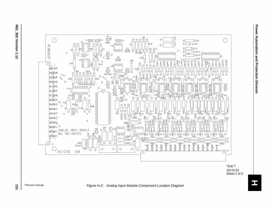
Pow
er Autom
ation and Protection D
ivision
RE
L 352 Version 1.12
131
H
*Denotes Change
*Sub 71611C23Sheet 2 of 3
Figure H-2: Analog Input Module Component Location Diagram

I.L. 40-201.9B Power Automation and Protection Division
132 REL 352 Version 1.12
*Sub 41612C20
* Denotes Change
Figure H-3: Analog Input Module Schematic (sheet 1 of 4)

Power Automation and Protection Division
REL 352 Version 1.12 133
H
Sub 41612C20
Figure H-3: Analog Input Module Schematic (Sheet 2 of 4)
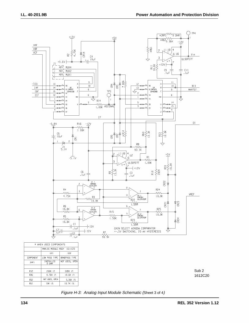
I.L. 40-201.9B Power Automation and Protection Division
134 REL 352 Version 1.12
Sub 21612C20
Figure H-3: Analog Input Module Schematic (Sheet 3 of 4)
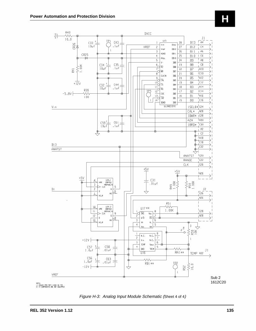
Power Automation and Protection Division
REL 352 Version 1.12 135
H
Sub 21612C20
Figure H-3: Analog Input Module Schematic (Sheet 4 of 4)

I.L. 40-201.9B Power Automation and Protection Division
136 REL 352 Version 1.12
THIS PAGE RESERVED FOR NOTES

Power Automation and Protection Division
REL 352 Version 1.12 • 137
I
1 INTRODUCTION
The acceptance test of the relay verifies the operation of four subsystems.
• Analog Input• Contact Input• Relay Output• Communication Interface
Additionally, Phase Comparison functional tests (simulating internal faults) are performed.
1.1 EQUIPMENT NEEDED
Qty. Description
1 REL 352 Relay1 Doble, AVO or equivalent 3-Phase Test System
1.2 TEST SETUP
1.2.1 Current and voltage Inputs
Connect the Relay Test System to REL 352 Relay, per application diagram 1618C33 (see SYSTEMDIAGRAMS section, Appendilx L, page 179 ). Please note that the Relay Test System SimulatesPower System shown on 1618C33.
! CAUTION
Do not leave the REL 352 with trip relays energized for long periods of time. Due tohigh power heat buildup, they are rated for intermittant duty only.
1.2.2 Power
Connect the primary and secondary dc power as shown on 1618C33. Consult the relay nameplatefor rated voltage.
NOTE: Before turning on dc power check jumper positions on the Optoisolated Input andMicroprocessor modules. (See pages page 103 and page 107)
1.3 ANALOG INPUT AND FRONT PANEL METERING TEST
STEP 1
Turn on the primary and optional secondary dc input power if used. Make sure that the FREQ set-ting matches the line frequency, and the RP setting is set to “NO” (Readout in secondary values).The “Relay in Service” LED on the front panel should be lit.
ACCEPTANCE TESTS

I.L. 40-201.9B Power Automation and Protection Division
138 • REL 352 Version 1.12
STEP 2
NOTE: All ac voltage & current phase angles in this document are referenced to VA-Gvoltage (0 degrees). Positive angles LEAD VA-G, negative angles LAG VA-G.
Fault impedance angles (FANG) are displayed as positive for inductive faults andnegative for capacitive.
Apply the following ac quantities to the relay:
Using the procedure described in Section 4, 4.2 , on page 40, read the following parameters:
Verify all metered values to be ± 5% on magnitude and ± 2 degrees on phase angle.
1.4 CONTACT INPUT SUBSYSTEM TEST
Make sure that the input voltage selection jumpers JMP7, JMP8, JMP9 on the optoisolated inputmodule 161838 (see figure 1-2, page 6) in Section 1 for module placement and figure D-1 (page104) in Appendix D for jumper location, correspond to the desired contacat "wetting" voltage.
Apply the rated voltage across the terminals shown in the table below:
Using procedure described in Section 4.4.1, (Section 4, page 41) verify proper response of thefront panel display to optoisolated status changes.
V (volts) / Angle I (amps) / Angle
Va = 70 ∠0°Vb = 70 ∠-120°Vc = 70 ∠+120°
Ia = 10 ∠-45°Ib = 10 ∠-165°Ic = 10 ∠+75°
VAG = 70∠VAG = 0VBG = 70∠VBG = -120VCG = 70∠VCG = +120IA = 10.0∠IA = -45IB = 10.0∠IB = -165IC = 10.0∠IC = +75
(VOLTS)(DEG.)(VOLTS)(DEG.)(VOLTS)(DEG.)(AMPS)(DEG.)(AMPS)(DEG.)(AMPS)(DEG.)
DescriptionTerminal
BlockTerminal+ -
HEXDigit
52bSTUB BUSTarget
TB5TB5TB5
1 23 45 6
102040
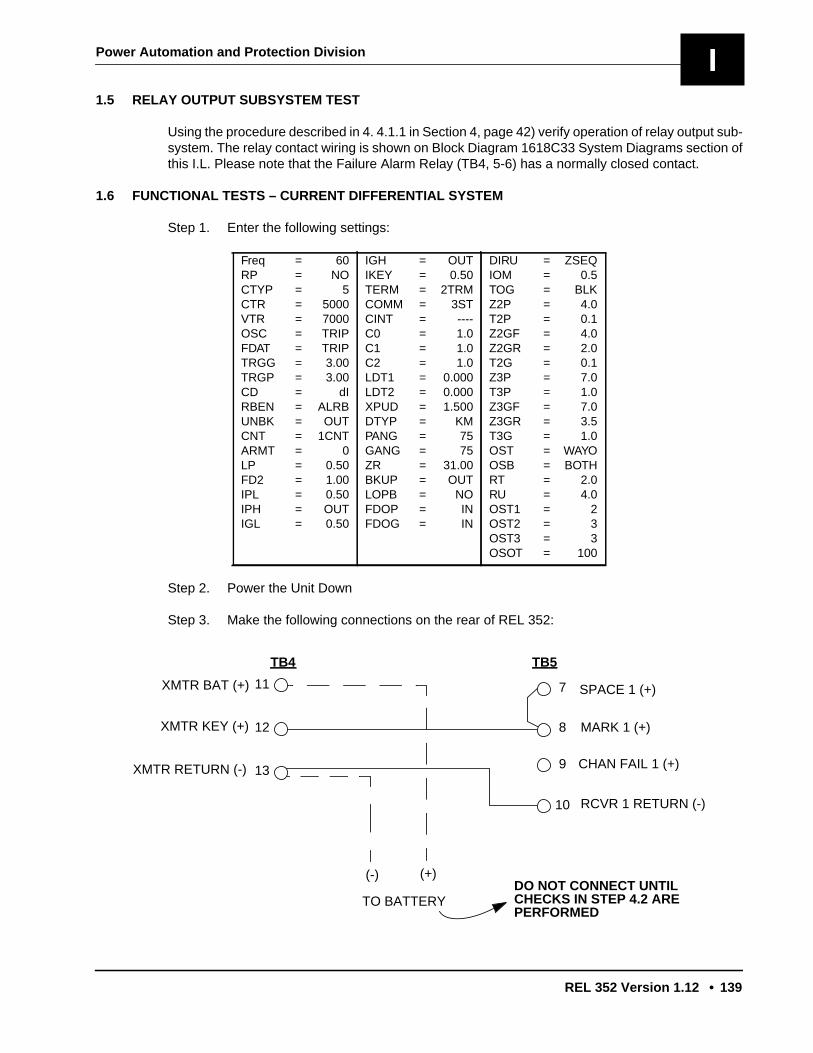
Power Automation and Protection Division
REL 352 Version 1.12 • 139
I1.5 RELAY OUTPUT SUBSYSTEM TEST
Using the procedure described in 4. 4.1.1 in Section 4, page 42) verify operation of relay output sub-system. The relay contact wiring is shown on Block Diagram 1618C33 System Diagrams section ofthis I.L. Please note that the Failure Alarm Relay (TB4, 5-6) has a normally closed contact.
1.6 FUNCTIONAL TESTS – CURRENT DIFFERENTIAL SYSTEM
Step 1. Enter the following settings:
Step 2. Power the Unit Down
Step 3. Make the following connections on the rear of REL 352:
Freq = 60RP = NOCTYP = 5CTR = 5000VTR = 7000OSC = TRIPFDAT = TRIPTRGG = 3.00TRGP = 3.00CD = dIRBEN = ALRBUNBK = OUTCNT = 1CNTARMT = 0LP = 0.50FD2 = 1.00IPL = 0.50IPH = OUTIGL = 0.50
IGH = OUTIKEY = 0.50TERM = 2TRMCOMM = 3STCINT = ----C0 = 1.0C1 = 1.0C2 = 1.0LDT1 = 0.000LDT2 = 0.000XPUD = 1.500DTYP = KMPANG = 75GANG = 75ZR = 31.00BKUP = OUTLOPB = NOFDOP = INFDOG = IN
DIRU = ZSEQIOM = 0.5TOG = BLKZ2P = 4.0T2P = 0.1Z2GF = 4.0Z2GR = 2.0T2G = 0.1Z3P = 7.0T3P = 1.0Z3GF = 7.0Z3GR = 3.5T3G = 1.0OST = WAYOOSB = BOTHRT = 2.0RU = 4.0OST1 = 2OST2 = 3OST3 = 3OSOT = 100
11
12
13
7
8
9
10
XMTR BAT (+)
XMTR KEY (+)
XMTR RETURN (-)
SPACE 1 (+)
MARK 1 (+)
CHAN FAIL 1 (+)
RCVR 1 RETURN (-)
(-) (+)
TO BATTERYDO NOT CONNECT UNTILCHECKS IN STEP 4.2 AREPERFORMED
TB4 TB5

I.L. 40-201.9B Power Automation and Protection Division
140 • REL 352 Version 1.12
Step 4. Remove inner chassis
a) Note factory settings of jumpers on Interconnect and Contact Input modules
b) Make sure that the jumpers; JMP4, JMP5 and JMP6 on Contact Input module and JMP7on Interconnect module are set for the desired battery voltage.
c) Set the following jumpers on Interconnect module:
JMP6 Normal (Key out)JMP5 Normal (SPACE 1)JMP 4 Inverted (MARK 1)JMP 1 Normal (Chann Fail)
Step 5. Insert and secure Inner chassis.
a) Power the unit up
b) Connect the battery as shown in diagram in step 3 above.
Step 6. Apply all types of faults greater than 3.0 A and verify relay’s response
For Example:
To simulate AG fault (zero sequence) apply: Ia = 3.0 AIb = 0 AIc = 0 A
For Example:
To simulate 3-phase fault (positive sequence) apply: Ia = 3.0 A at 0˚Ib = 3.0 A at -120˚Ic = 3.0 A at +120˚
1.7 FUNCTIONAL TESTS - Optional Backup System
For units that include the stepped distance backup system the following tests will functionalyy testall the distance units provided.
Conntect terminal TB5-9 (Channel Failure) to battery (+). This generates channel failure state, dis-ables phase comparison and activates distance backup system.
Verify that a metering mode CHRX display reads CHTB.
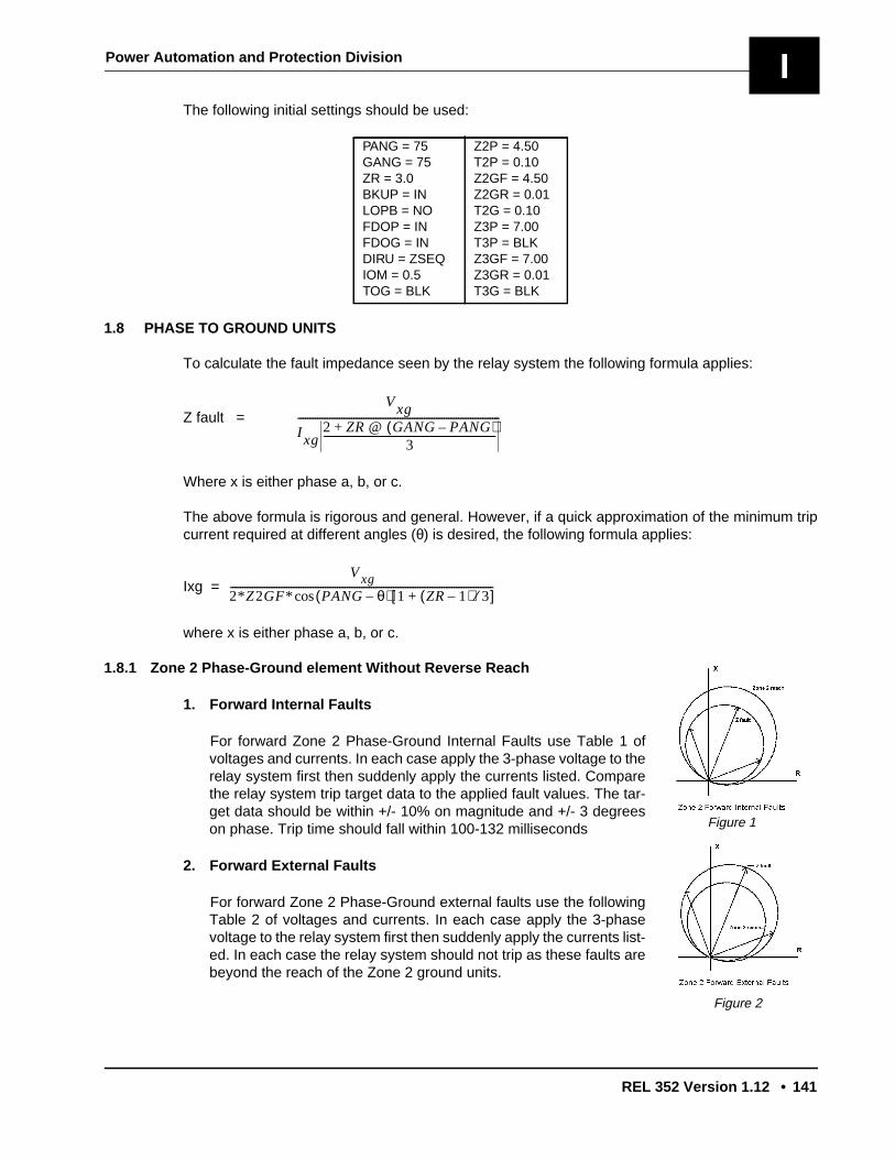
Power Automation and Protection Division
REL 352 Version 1.12 • 141
IThe following initial settings should be used:
1.8 PHASE TO GROUND UNITS
To calculate the fault impedance seen by the relay system the following formula applies:
Z fault =
Where x is either phase a, b, or c.
The above formula is rigorous and general. However, if a quick approximation of the minimum tripcurrent required at different angles (θ) is desired, the following formula applies:
Ixg =
where x is either phase a, b, or c.
1.8.1 Zone 2 Phase-Ground element Without Reverse Reach
1. Forward Internal Faults
For forward Zone 2 Phase-Ground Internal Faults use Table 1 ofvoltages and currents. In each case apply the 3-phase voltage to therelay system first then suddenly apply the currents listed. Comparethe relay system trip target data to the applied fault values. The tar-get data should be within +/- 10% on magnitude and +/- 3 degreeson phase. Trip time should fall within 100-132 milliseconds
2. Forward External Faults
For forward Zone 2 Phase-Ground external faults use the followingTable 2 of voltages and currents. In each case apply the 3-phasevoltage to the relay system first then suddenly apply the currents list-ed. In each case the relay system should not trip as these faults arebeyond the reach of the Zone 2 ground units.
PANG = 75GANG = 75ZR = 3.0BKUP = INLOPB = NOFDOP = INFDOG = INDIRU = ZSEQIOM = 0.5TOG = BLK
Z2P = 4.50T2P = 0.10Z2GF = 4.50Z2GR = 0.01T2G = 0.10Z3P = 7.00T3P = BLKZ3GF = 7.00Z3GR = 0.01T3G = BLK
Vxg
I xg2 ZR @ GANG PANG–( )+
3-----------------------------------------------------------------------
-----------------------------------------------------------------------------------
Vxg2*Z2GF* PANG θ–( ) 1 ZR 1–( ) 3⁄+[ ]cos------------------------------------------------------------------------------------------------------------
Figure 1
Figure 2

I.L. 40-201.9B Power Automation and Protection Division
142 • REL 352 Version 1.12
Table 1:Zone 2 Phase-Ground Forward Internal Faults:
Z2GF = 4.5 Ohms Z2GR = 0.01 Ohms
VVolts ∠ Angle
IAmps ∠ Angle
Fault ZOhms ∠ Ang
Relay SystemOperation
AG at MTA 90% of reach fault
Va = 30 ∠ 0Vb = 69 ∠ -120 (240)Vc = 69 ∠ -240 (120)
Ia = 4.4 ∠ -75 (285)Ib = 0Ic = 0
4.05 ∠ 75 Z2T TripFault type AGZ2G UnitTrip time 100-132 mS
AG at MTA -45˚ 90% of reach fault
Va = 30 ∠ 0Vb = 69 ∠ -120 (240)Vc = 69 ∠ -240 (120)
Ia = 6.23 ∠ -30 (330)Ib = 0Ic = 0
2.86 ∠ 30 Z2T TripFault type AGZ2G UnitTrip time 100-132 mS
AG at MTA +45˚ 90% of reach fault
Va = 30 ∠ 0Vb = 69 ∠ -120 (240)Vc = 69 ∠ -240 (120)
Ia = 6.23 ∠ -120 (240)Ib = 0Ic = 0
2.86 ∠ 120 Z2T TripFault type AGZ2G UnitTrip time 100-132 mS
BG at MTA 90% of reach fault
Va = 69 ∠ 0Vb = 30 ∠ -120 (240)Vc = 69 ∠ -240 (120)
Ia = 0Ib = 4.4 ∠ -195 (165)Ic = 0
4.05 ∠ 75 Z2T TripFault type BGZ2G UnitTrip time 100-132 mS
BG at MTA -45˚ 90% of reach fault
Va = 69 ∠ 0Vb = 30 ∠ -120 (240)Vc = 69 ∠ -240 (120)
Ia = 0Ib = 6.23 ∠ -150 (210)Ic = 0
2.86 ∠ 30 Z2T TripFault type BGZ2G UnitTrip time 100-132 mS
BG at MTA +45˚ 90% of reach fault
Va = 69 ∠ 0Vb = 30 ∠ -120 (240)Vc = 69 ∠ -240 (120)
Ia = 0Ib = 6.23 ∠ -240 120)Ic = 0
2.86 ∠ 120 Z2T TripFault type BGZ2G UnitTrip time 100-132 mS
CG at MTA 90% of reach fault
Va = 69 ∠ 0Vb = 69 ∠ -120 (240)Vc = 30 ∠ -240 (120)
Ia = 0Ib = 0Ic = 4.4 ∠ -315 (45)
4.05 ∠ 75 Z2T TripFault type CGZ2G UnitTrip time 100-132 mS
CG at MTA -45˚ 90% of reach fault
Va = 69 ∠ 0Vb = 69 ∠ -120 (240)Vc = 30 ∠ -240 (120)
Ia = 0Ib = 0Ic = 6.23 ∠ -270 (90)
2.86 ∠ 30 Z2T TripFault type CGZ2G UnitTrip time 100-132 mS
CG at MTA +45˚ 90% of reach fault
Va = 69 ∠ 0Vb = 69 ∠ -120 (240)Vc = 30 ∠ -240 (120)
Ia = 0Ib = 0Ic = 6.23 ∠ 0
2.86 ∠ 120 Z2T TripFault type CGZ2G UnitTrip time 100-132 mS

Power Automation and Protection Division
REL 352 Version 1.12 • 143
ITable 2:
Zone 2 Forward Phase-Ground External Faults:Z2GF = 4.5 Ohms Z2RG = 0.01 Ohms
VVolts ∠ Angle
IAmps ∠ Angle
Fault ZOhms ∠ Ang
Relay SystemOperation
AG at MTA 110% of reach fault
Va = 30 ∠ 0Vb = 69 ∠ -120 (240)Vc = 69 ∠ -240 (120)
Ia = 3.6 ∠ -75 (285)Ib = 0Ic = 0
4.95 ∠ 75 No Trips
AG at MTA -45˚ 110% of reach fault
Va = 30 ∠ 0Vb = 69 ∠ -120 (240)Vc = 69 ∠ -240 (120)
Ia = 5.09 ∠ -30 (330)Ib = 0Ic = 0
3.5 ∠ 30 No Trips
AG at MTA +45˚ 110% of reach fault
Va = 30 ∠ 0Vb = 69 ∠ -120 (240)Vc = 69 ∠ -240 (120)
Ia = 5.09 ∠ -120 (240)Ib = 0Ic = 0
3.5 ∠ 120 No Trips
BG at MTA 110% of reach fault
Va = 69 ∠ 0Vb = 30 ∠ -120 (240)Vc = 69 ∠ -240 (120)
Ia = 0Ib = 3.6 ∠ -195 (165)Ic = 0
4.95 ∠ 75 No Trips
BG at MTA -45˚ 110% of reach fault
Va = 69 ∠ 0Vb = 30 ∠ -120 (240)Vc = 69 ∠ -240 (120)
Ia = 0Ib = 5.09 ∠ -150 (210)Ic = 0
3.5 ∠ 30 No Trips
BG at MTA +45˚ 110% of reach fault
Va = 69 ∠ 0Vb = 30 ∠ -120 (240)Vc = 69 ∠ -240 (120)
Ia = 0Ib = 5.09 ∠ -240 120)Ic = 0
3.5 ∠ 120 No Trips
CG at MTA 110% of reach fault
Va = 69 ∠ 0Vb = 69 ∠ -120 (240)Vc = 30 ∠ -240 (120)
Ia = 0Ib = 0Ic = 3.6 ∠ -315 (45)
4.95 ∠ 75 No Trips
CG at MTA -45˚ 110% of reach fault
Va = 69 ∠ 0Vb = 69 ∠ -120 (240)Vc = 30 ∠ -240 (120)
Ia = 0Ib = 0Ic =5.09 ∠ -270 (90)
3.5 ∠ 30 No Trips
CG at MTA +45˚ 110% of reach fault
Va = 69 ∠ 0Vb = 69 ∠ -120 (240)Vc = 30 ∠ -240 (120)
Ia = 0Ib = 0Ic = 5.09 ∠ 0
3.5 ∠ 120 No Trips

I.L. 40-201.9B Power Automation and Protection Division
144 • REL 352 Version 1.12
3. Reverse External Faults
For reverse Zone 2 Phase-Ground external faults see Table 3of voltages and currents. In each case apply the 3-phase volt-age to the relay system first then suddenly apply the currentslisted. In each case the relay system should not trip as thesefaults are reverse direction from the GANG setting.
Figure 3
1.8.2 Zone 2 Phase-Ground element with Reverse Reach
NOTE: Change the “Z2GR” distance setting to 4.5 ohms before applying the followingfaults in Tables 4, 5, and 6 to the relay system.
4. Forward Internal Faults
For forward Zone 2 Phase-Ground internal faults use thefollowing Table 4 of voltages and currents. In each case ap-ply the 3-phase voltage to the relay system first then sud-denly apply the currents listed. Compare the relay systemtrip target data to the applied fault values. The target datashould be within +/- 10% on magnitude and +/- 3 degreeson phase. Trip time should fall within 100-132 milliseconds.
Table 3:Zone 2 Phase-Ground Reverse External Faults:
Z2GF = 4.5 Ohms Z2GR = 0.01 Ohms
VVolts ∠ Angle
IAmps ∠ Angle
Fault ZOhms ∠ Ang
Relay SystemOperation
AG at MTA -180˚ 50% of reach fault
Va = 30 ∠ 0Vb = 69 ∠ -120 (240)Vc = 69 ∠ -240 (120)
Ia = 8 ∠ -255 (105)Ib = 0Ic = 0 2.25 ∠ -105 No Trips
BG at MTA -180˚ 50% of reach fault
Va = 69 ∠ 0Vb = 30 ∠ -120 (240)Vc = 69 ∠ -240 (120)
Ia = 0Ib = 8 ∠ -15 (345)Ic = 0 2.25 ∠ -105 No Trips
CG at MTA -180˚ 50% of reach fault
Va = 69 ∠ 0Vb = 69 ∠ -120 (240)Vc = 30 ∠ -240 (120)
Ia = 0Ib = 0Ic = 8 ∠ -135 (225) 2.25 ∠ -105 No Trips
Figure 4
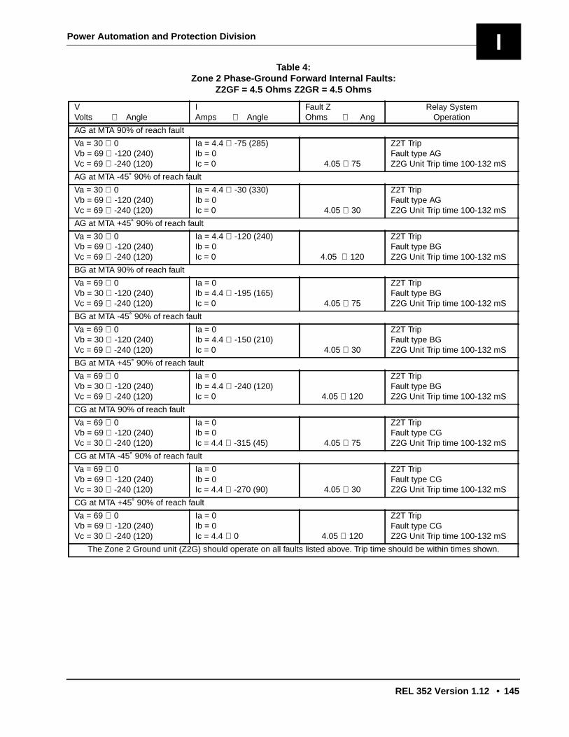
Power Automation and Protection Division
REL 352 Version 1.12 • 145
ITable 4:
Zone 2 Phase-Ground Forward Internal Faults:Z2GF = 4.5 Ohms Z2GR = 4.5 Ohms
VVolts ∠ Angle
IAmps ∠ Angle
Fault ZOhms ∠ Ang
Relay SystemOperation
AG at MTA 90% of reach fault
Va = 30 ∠ 0Vb = 69 ∠ -120 (240)Vc = 69 ∠ -240 (120)
Ia = 4.4 ∠ -75 (285)Ib = 0Ic = 0 4.05 ∠ 75
Z2T TripFault type AGZ2G Unit Trip time 100-132 mS
AG at MTA -45˚ 90% of reach fault
Va = 30 ∠ 0Vb = 69 ∠ -120 (240)Vc = 69 ∠ -240 (120)
Ia = 4.4 ∠ -30 (330)Ib = 0Ic = 0 4.05 ∠ 30
Z2T TripFault type AGZ2G Unit Trip time 100-132 mS
AG at MTA +45˚ 90% of reach fault
Va = 30 ∠ 0Vb = 69 ∠ -120 (240)Vc = 69 ∠ -240 (120)
Ia = 4.4 ∠ -120 (240)Ib = 0Ic = 0 4.05 ∠ 120
Z2T TripFault type BGZ2G Unit Trip time 100-132 mS
BG at MTA 90% of reach fault
Va = 69 ∠ 0Vb = 30 ∠ -120 (240)Vc = 69 ∠ -240 (120)
Ia = 0Ib = 4.4 ∠ -195 (165)Ic = 0 4.05 ∠ 75
Z2T TripFault type BGZ2G Unit Trip time 100-132 mS
BG at MTA -45˚ 90% of reach fault
Va = 69 ∠ 0Vb = 30 ∠ -120 (240)Vc = 69 ∠ -240 (120)
Ia = 0Ib = 4.4 ∠ -150 (210)Ic = 0 4.05 ∠ 30
Z2T TripFault type BGZ2G Unit Trip time 100-132 mS
BG at MTA +45˚ 90% of reach fault
Va = 69 ∠ 0Vb = 30 ∠ -120 (240)Vc = 69 ∠ -240 (120)
Ia = 0Ib = 4.4 ∠ -240 (120)Ic = 0 4.05 ∠ 120
Z2T TripFault type BGZ2G Unit Trip time 100-132 mS
CG at MTA 90% of reach fault
Va = 69 ∠ 0Vb = 69 ∠ -120 (240)Vc = 30 ∠ -240 (120)
Ia = 0Ib = 0Ic = 4.4 ∠ -315 (45) 4.05 ∠ 75
Z2T TripFault type CGZ2G Unit Trip time 100-132 mS
CG at MTA -45˚ 90% of reach fault
Va = 69 ∠ 0Vb = 69 ∠ -120 (240)Vc = 30 ∠ -240 (120)
Ia = 0Ib = 0Ic = 4.4 ∠ -270 (90) 4.05 ∠ 30
Z2T TripFault type CGZ2G Unit Trip time 100-132 mS
CG at MTA +45˚ 90% of reach fault
Va = 69 ∠ 0Vb = 69 ∠ -120 (240)Vc = 30 ∠ -240 (120)
Ia = 0Ib = 0Ic = 4.4 ∠ 0 4.05 ∠ 120
Z2T TripFault type CGZ2G Unit Trip time 100-132 mS
The Zone 2 Ground unit (Z2G) should operate on all faults listed above. Trip time should be within times shown.
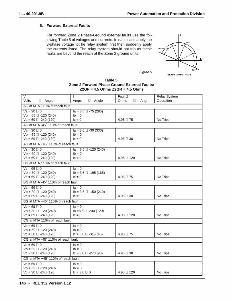
I.L. 40-201.9B Power Automation and Protection Division
146 • REL 352 Version 1.12
5. Forward External Faults
For forward Zone 2 Phase-Ground external faults use the fol-lowing Table 5 of voltages and currents. In each case apply the3-phase voltage tot he relay system first then suddenly applythe currents listed. The relay system should not trip as thesefaults are beyond the reach of the Zone 2 ground units.
Figure 5
Table 5:Zone 2 Forward Phase-Ground External Faults:
Z2GF = 4.5 Ohms Z2GR = 4.5 Ohms
VVolts ∠ Angle
IAmps ∠ Angle
Fault ZOhms ∠ Ang
Relay SystemOperation
AG at MTA 110% of reach fault
Va = 30 ∠ 0Vb = 69 ∠ -120 (240)Vc = 69 ∠ -240 (120)
Ia = 3.6 ∠ -75 (285)Ib = 0Ic = 0 4.95 ∠ 75 No Trips
AG at MTA -45˚ 110% of reach fault
Va = 30 ∠ 0Vb = 69 ∠ -120 (240)Vc = 69 ∠ -240 (120)
Ia = 3.6 ∠ -30 (330)Ib = 0Ic = 0 4.95 ∠ 30 No Trips
AG at MTA +45˚ 110% of reach fault
Va = 30 ∠ 0Vb = 69 ∠ -120 (240)Vc = 69 ∠ -240 (120)
Ia = 3.6 ∠ -120 (240)Ib = 0Ic = 0 4.95 ∠ 120 No Trips
BG at MTA 110% of reach fault
Va = 69 ∠ 0Vb = 30 ∠ -120 (240)Vc = 69 ∠ -240 (120)
Ia = 0Ib = 3.6 ∠ -195 (165)Ic = 0 4.95 ∠ 75 No Trips
BG at MTA -45˚ 110% of reach fault
Va = 69 ∠ 0Vb = 30 ∠ -120 (240)Vc = 69 ∠ -240 (120)
Ia = 0Ib = 3.6 ∠ -150 (210)Ic = 0 4.95 ∠ 30 No Trips
BG at MTA +45˚ 110% of reach fault
Va = 69 ∠ 0Vb = 30 ∠ -120 (240)Vc = 69 ∠ -240 (120)
Ia = 0Ib =3.6 ∠ -240 (120)Ic = 0 4.95 ∠ 120 No Trips
CG at MTA 110% of reach fault
Va = 69 ∠ 0Vb = 69 ∠ -120 (240)Vc = 30 ∠ -240 (120)
Ia = 0Ib = 0Ic = 3.6 ∠ -315 (45) 4.95 ∠ 75 No Trips
CG at MTA -45˚ 110% of reach fault
Va = 69 ∠ 0Vb = 69 ∠ -120 (240)Vc = 30 ∠ -240 (120)
Ia = 0Ib = 0Ic = 3.6 ∠ -270 (90) 4.95 ∠ 30 No Trips
CG at MTA +45˚ 110% of reach fault
Va = 69 ∠ 0Vb = 69 ∠ -120 (240)Vc = 30 ∠ -240 (120)
Ia = 0Ib = 0Ic = 3.6 ∠ 0 4.95 ∠ 120 No Trips
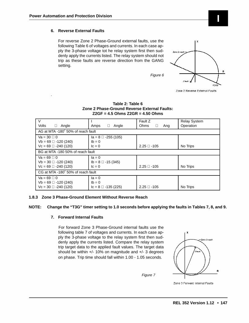
Power Automation and Protection Division
REL 352 Version 1.12 • 147
I6. Reverse External Faults
For reverse Zone 2 Phase-Ground external faults, use thefollowing Table 6 of voltages and currents. In each case ap-ply the 3-phase voltage tot he relay system first then sud-denly apply the currents listed. The relay system should nottrip as these faults are reverse direction from the GANGsetting.
Figure 6
.
1.8.3 Zone 3 Phase-Ground Element Without Reverse Reach
NOTE: Change the “T3G” timer setting to 1.0 seconds before applying the faults in Tables 7, 8, and 9.
7. Forward Internal Faults
For forward Zone 3 Phase-Ground internal faults use thefollowing table 7 of voltages and currents. In each case ap-ply the 3-phase voltage to the relay system first then sud-denly apply the currents listed. Compare the relay systemtrip target data to the applied fault values. The target datashould be within +/- 10% on magnitude and +/- 3 degreeson phase. Trip time should fall within 1.00 - 1.05 seconds.
Table 2: Table 6Zone 2 Phase-Ground Reverse External Faults:
Z2GF = 4.5 Ohms Z2GR = 4.50 Ohms
VVolts ∠ Angle
IAmps ∠ Angle
Fault ZOhms ∠ Ang
Relay SystemOperation
AG at MTA -180˚ 50% of reach fault
Va = 30 ∠ 0Vb = 69 ∠ -120 (240)Vc = 69 ∠ -240 (120)
Ia = 8 ∠ -255 (105)Ib = 0Ic = 0 2.25 ∠ -105 No Trips
BG at MTA -180 50% of reach fault
Va = 69 ∠ 0Vb = 30 ∠ -120 (240)Vc = 69 ∠ -240 (120)
Ia = 0Ib = 8 ∠ -15 (345)Ic = 0 2.25 ∠ -105 No Trips
CG at MTA -180˚ 50% of reach fault
Va = 69 ∠ 0Vb = 69 ∠ -120 (240)Vc = 30 ∠ -240 (120)
Ia = 0Ib = 0Ic = 8 ∠ -135 (225) 2.25 ∠ -105 No Trips
Figure 7
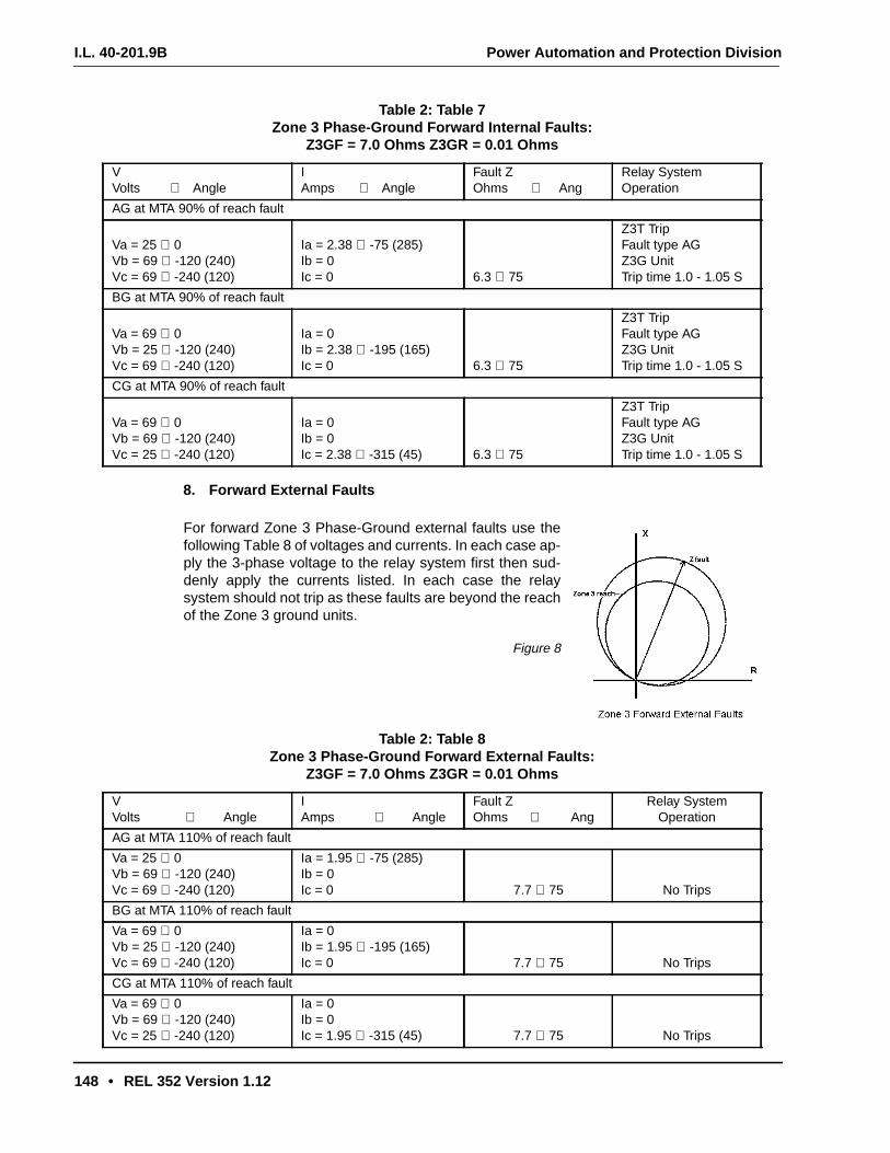
I.L. 40-201.9B Power Automation and Protection Division
148 • REL 352 Version 1.12
8. Forward External Faults
For forward Zone 3 Phase-Ground external faults use thefollowing Table 8 of voltages and currents. In each case ap-ply the 3-phase voltage to the relay system first then sud-denly apply the currents listed. In each case the relaysystem should not trip as these faults are beyond the reachof the Zone 3 ground units.
Figure 8
Table 2: Table 7Zone 3 Phase-Ground Forward Internal Faults:
Z3GF = 7.0 Ohms Z3GR = 0.01 Ohms
VVolts ∠ Angle
IAmps ∠ Angle
Fault ZOhms ∠ Ang
Relay SystemOperation
AG at MTA 90% of reach fault
Va = 25 ∠ 0Vb = 69 ∠ -120 (240)Vc = 69 ∠ -240 (120)
Ia = 2.38 ∠ -75 (285)Ib = 0Ic = 0 6.3 ∠ 75
Z3T TripFault type AGZ3G UnitTrip time 1.0 - 1.05 S
BG at MTA 90% of reach fault
Va = 69 ∠ 0Vb = 25 ∠ -120 (240)Vc = 69 ∠ -240 (120)
Ia = 0Ib = 2.38 ∠ -195 (165)Ic = 0 6.3 ∠ 75
Z3T TripFault type AGZ3G UnitTrip time 1.0 - 1.05 S
CG at MTA 90% of reach fault
Va = 69 ∠ 0Vb = 69 ∠ -120 (240)Vc = 25 ∠ -240 (120)
Ia = 0Ib = 0Ic = 2.38 ∠ -315 (45) 6.3 ∠ 75
Z3T TripFault type AGZ3G UnitTrip time 1.0 - 1.05 S
Table 2: Table 8Zone 3 Phase-Ground Forward External Faults:
Z3GF = 7.0 Ohms Z3GR = 0.01 Ohms
VVolts ∠ Angle
IAmps ∠ Angle
Fault ZOhms ∠ Ang
Relay SystemOperation
AG at MTA 110% of reach fault
Va = 25 ∠ 0Vb = 69 ∠ -120 (240)Vc = 69 ∠ -240 (120)
Ia = 1.95 ∠ -75 (285)Ib = 0Ic = 0 7.7 ∠ 75 No Trips
BG at MTA 110% of reach fault
Va = 69 ∠ 0Vb = 25 ∠ -120 (240)Vc = 69 ∠ -240 (120)
Ia = 0Ib = 1.95 ∠ -195 (165)Ic = 0 7.7 ∠ 75 No Trips
CG at MTA 110% of reach fault
Va = 69 ∠ 0Vb = 69 ∠ -120 (240)Vc = 25 ∠ -240 (120)
Ia = 0Ib = 0Ic = 1.95 ∠ -315 (45) 7.7 ∠ 75 No Trips

Power Automation and Protection Division
REL 352 Version 1.12 • 149
I9. Reverse External Faults
For reverse Zone 3 Phase-Ground external faults use thefollowing Table 9 of voltages and currents. In each case ap-ply the 3-phase voltage to the relay system first then sud-denly apply the currents listed. In each case the relaysystem should not trip as these faults are reverse directionfrom the GANG setting.
Figure 9
1.8.4 Phase to Phase Units
To calculate the fault impedance seen by the relay system the following formula applies:
Z fault =
where x is either phase a, b, or c and y is the next lagging phase.
The above formula is rigorous and general. However, if a quick approximation of the minimum tripcurrent required at different angles (θ) is desired, the following formula applies:
lxy =
where x is either phase a, b, or c and y is the next lagging phase.
Table 2: Table 9Zone 3 Phase-Ground Reverse External Faults:
Z3GF = 7.0 Ohms Z3GR = 0.01 Ohms
VVolts ∠ Angle
IAmps ∠ Angle
Fault ZOhms ∠ Ang
Relay SystemOperation
AG at MTA -180˚ 50% of reach fault
Va = 25 ∠ 0Vb = 69 ∠ -120 (240)Vc = 69 ∠ -240 (120)
Ia = 4.29 ∠ -255 (105)Ib = 0Ic = 0 3.5 ∠ -105 No Trips
BG at MTA-180˚ 50% of reach fault
Va = 69 ∠ 0Vb = 25 ∠ -120 (240)Vc = 69 ∠ -240 (120)
Ia = 0Ib = 4.29 ∠ -15 (345)Ic = 0 3.5 ∠ -105 No Trips
CG at MTA -180˚ 50% of reach fault
Va = 69 ∠ 0Vb = 69 ∠ -120 (240)Vc = 25 ∠ -240 (120)
Ia = 0Ib = 0Ic = 4.29 ∠ -135 (225) 3.5 ∠ -105 No Trips
VxyIx ly–---------------
VxyZ2P PANG θ–( )cos( )-----------------------------------------------------
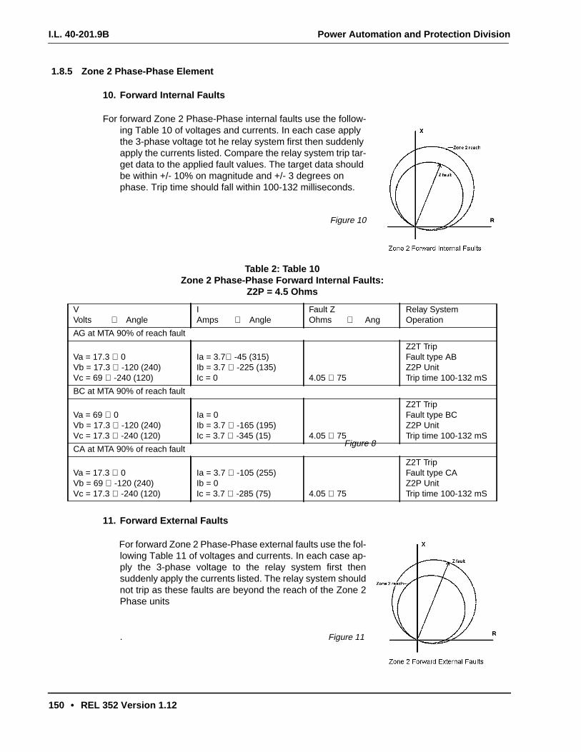
I.L. 40-201.9B Power Automation and Protection Division
150 • REL 352 Version 1.12
1.8.5 Zone 2 Phase-Phase Element
10. Forward Internal Faults
For forward Zone 2 Phase-Phase internal faults use the follow-ing Table 10 of voltages and currents. In each case applythe 3-phase voltage tot he relay system first then suddenlyapply the currents listed. Compare the relay system trip tar-get data to the applied fault values. The target data shouldbe within +/- 10% on magnitude and +/- 3 degrees onphase. Trip time should fall within 100-132 milliseconds.
Figure 10
11. Forward External Faults
For forward Zone 2 Phase-Phase external faults use the fol-lowing Table 11 of voltages and currents. In each case ap-ply the 3-phase voltage to the relay system first thensuddenly apply the currents listed. The relay system shouldnot trip as these faults are beyond the reach of the Zone 2Phase units
. Figure 11
Table 2: Table 10Zone 2 Phase-Phase Forward Internal Faults:
Z2P = 4.5 Ohms
VVolts ∠ Angle
IAmps ∠ Angle
Fault ZOhms ∠ Ang
Relay SystemOperation
AG at MTA 90% of reach fault
Va = 17.3 ∠ 0Vb = 17.3 ∠ -120 (240)Vc = 69 ∠ -240 (120)
Ia = 3.7∠ -45 (315)Ib = 3.7 ∠ -225 (135)Ic = 0 4.05 ∠ 75
Z2T TripFault type ABZ2P UnitTrip time 100-132 mS
BC at MTA 90% of reach fault
Va = 69 ∠ 0Vb = 17.3 ∠ -120 (240)Vc = 17.3 ∠ -240 (120)
Ia = 0Ib = 3.7 ∠ -165 (195)Ic = 3.7 ∠ -345 (15) 4.05 ∠ 75
Z2T TripFault type BCZ2P UnitTrip time 100-132 mS
CA at MTA 90% of reach fault
Va = 17.3 ∠ 0Vb = 69 ∠ -120 (240)Vc = 17.3 ∠ -240 (120)
Ia = 3.7 ∠ -105 (255)Ib = 0Ic = 3.7 ∠ -285 (75) 4.05 ∠ 75
Z2T TripFault type CAZ2P UnitTrip time 100-132 mS
Figure 8
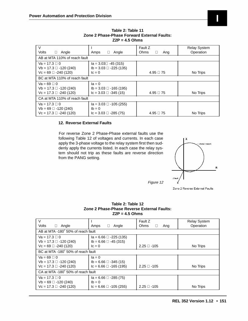
Power Automation and Protection Division
REL 352 Version 1.12 • 151
I
12. Reverse External Faults
For reverse Zone 2 Phase-Phase external faults use thefollowing Table 12 of voltages and currents. In each caseapply the 3-phase voltage to the relay system first then sud-denly apply the currents listed. In each case the relay sys-tem should not trip as these faults are reverse directionfrom the PANG setting.
Figure 12
Table 2: Table 11Zone 2 Phase-Phase Forward External Faults:
Z2P = 4.5 Ohms
VVolts ∠ Angle
IAmps ∠ Angle
Fault ZOhms ∠ Ang
Relay SystemOperation
AB at MTA 110% of reach fault
Va = 17.3 ∠ 0Vb = 17.3 ∠ -120 (240)Vc = 69 ∠ -240 (120)
Ia = 3.03∠ -45 (315)Ib = 3.03 ∠ -225 (135)Ic = 0 4.95 ∠ 75 No Trips
BC at MTA 110% of reach fault
Va = 69 ∠ 0Vb = 17.3 ∠ -120 (240)Vc = 17.3 ∠ -240 (120)
Ia = 0Ib = 3.03 ∠ -165 (195)Ic = 3.03 ∠ -345 (15) 4.95 ∠ 75 No Trips
CA at MTA 110% of reach fault
Va = 17.3 ∠ 0Vb = 69 ∠ -120 (240)Vc = 17.3 ∠ -240 (120)
Ia = 3.03 ∠ -105 (255)Ib = 0Ic = 3.03 ∠ -285 (75) 4.95 ∠ 75 No Trips
Table 2: Table 12Zone 2 Phase-Phase Reverse External Faults:
Z2P = 4.5 Ohms
VVolts ∠ Angle
IAmps ∠ Angle
Fault ZOhms ∠ Ang
Relay SystemOperation
AB at MTA -180˚ 50% of reach fault
Va = 17.3 ∠ 0Vb = 17.3 ∠ -120 (240)Vc = 69 ∠ -240 (120)
Ia = 6.66 ∠ -225 (135)Ib = 6.66 ∠ -45 (315)Ic = 0 2.25 ∠ -105 No Trips
BC at MTA -180˚ 50% of reach fault
Va = 69 ∠ 0Vb = 17.3 ∠ -120 (240)Vc = 17.3 ∠ -240 (120)
Ia = 0Ib = 6.66 ∠ -345 (15)Ic = 6.66 ∠ -165 (195) 2.25 ∠ -105 No Trips
CA at MTA -180˚ 50% of reach fault
Va = 17.3 ∠ 0Vb = 69 ∠ -120 (240)Vc = 17.3 ∠ -240 (120)
Ia = 6.66 ∠ -285 (75)Ib = 0Ic = 6.66 ∠ -105 (255) 2.25 ∠ -105 No Trips
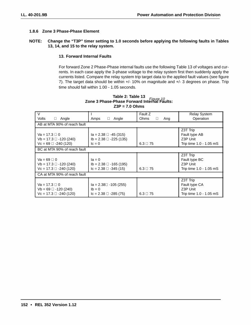
I.L. 40-201.9B Power Automation and Protection Division
152 • REL 352 Version 1.12
1.8.6 Zone 3 Phase-Phase Element
NOTE: Change the “T3P” timer setting to 1.0 seconds before applying the following faults in Tables13, 14, and 15 to the relay system.
13. Forward Internal Faults
For forward Zone 2 Phase-Phase internal faults use the following Table 13 of voltages and cur-rents. In each case apply the 3-phase voltage to the relay system first then suddenly apply thecurrents listed. Compare the relay system trip target data to the applied fault values (see figure7). The target data should be within +/- 10% on magnitude and +/- 3 degrees on phase. Triptime should fall within 1.00 - 1.05 seconds.
Table 2: Table 13Zone 3 Phase-Phase Forward Internal Faults:
Z3P = 7.0 Ohms
VVolts ∠ Angle
IAmps ∠ Angle
Fault ZOhms ∠ Ang
Relay SystemOperation
AB at MTA 90% of reach fault
Va = 17.3 ∠ 0Vb = 17.3 ∠ -120 (240)Vc = 69 ∠ -240 (120)
Ia = 2.38 ∠ -45 (315)Ib = 2.38 ∠ -225 (135)Ic = 0 6.3 ∠ 75
Z3T TripFault type ABZ3P UnitTrip time 1.0 - 1.05 mS
BC at MTA 90% of reach fault
Va = 69 ∠ 0Vb = 17.3 ∠ -120 (240)Vc = 17.3 ∠ -240 (120)
Ia = 0Ib = 2.38 ∠ -165 (195)Ic = 2.38 ∠ -345 (15) 6.3 ∠ 75
Z3T TripFault type BCZ3P UnitTrip time 1.0 - 1.05 mS
CA at MTA 90% of reach fault
Va = 17.3 ∠ 0Vb = 69 ∠ -120 (240)Vc = 17.3 ∠ -240 (120)
Ia = 2.38∠ -105 (255)Ib = 0Ic = 2.38 ∠ -285 (75) 6.3 ∠ 75
Z3T TripFault type CAZ3P UnitTrip time 1.0 - 1.05 mS
Figure 10
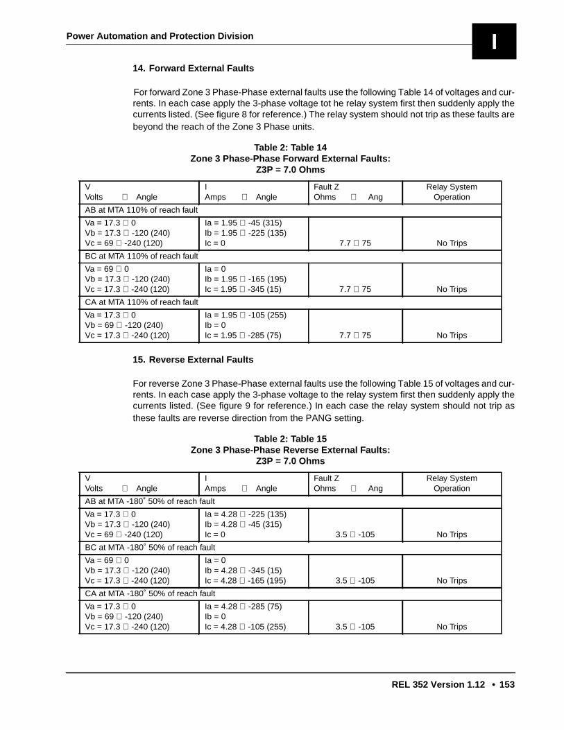
Power Automation and Protection Division
REL 352 Version 1.12 • 153
I14. Forward External Faults
For forward Zone 3 Phase-Phase external faults use the following Table 14 of voltages and cur-rents. In each case apply the 3-phase voltage tot he relay system first then suddenly apply thecurrents listed. (See figure 8 for reference.) The relay system should not trip as these faults arebeyond the reach of the Zone 3 Phase units.
15. Reverse External Faults
For reverse Zone 3 Phase-Phase external faults use the following Table 15 of voltages and cur-rents. In each case apply the 3-phase voltage to the relay system first then suddenly apply thecurrents listed. (See figure 9 for reference.) In each case the relay system should not trip asthese faults are reverse direction from the PANG setting.
Table 2: Table 14Zone 3 Phase-Phase Forward External Faults:
Z3P = 7.0 Ohms
VVolts ∠ Angle
IAmps ∠ Angle
Fault ZOhms ∠ Ang
Relay SystemOperation
AB at MTA 110% of reach fault
Va = 17.3 ∠ 0Vb = 17.3 ∠ -120 (240)Vc = 69 ∠ -240 (120)
Ia = 1.95 ∠ -45 (315)Ib = 1.95 ∠ -225 (135)Ic = 0 7.7 ∠ 75 No Trips
BC at MTA 110% of reach fault
Va = 69 ∠ 0Vb = 17.3 ∠ -120 (240)Vc = 17.3 ∠ -240 (120)
Ia = 0Ib = 1.95 ∠ -165 (195)Ic = 1.95 ∠ -345 (15) 7.7 ∠ 75 No Trips
CA at MTA 110% of reach fault
Va = 17.3 ∠ 0Vb = 69 ∠ -120 (240)Vc = 17.3 ∠ -240 (120)
Ia = 1.95 ∠ -105 (255)Ib = 0Ic = 1.95 ∠ -285 (75) 7.7 ∠ 75 No Trips
Table 2: Table 15Zone 3 Phase-Phase Reverse External Faults:
Z3P = 7.0 Ohms
VVolts ∠ Angle
IAmps ∠ Angle
Fault ZOhms ∠ Ang
Relay SystemOperation
AB at MTA -180˚ 50% of reach fault
Va = 17.3 ∠ 0Vb = 17.3 ∠ -120 (240)Vc = 69 ∠ -240 (120)
Ia = 4.28 ∠ -225 (135)Ib = 4.28 ∠ -45 (315)Ic = 0 3.5 ∠ -105 No Trips
BC at MTA -180˚ 50% of reach fault
Va = 69 ∠ 0Vb = 17.3 ∠ -120 (240)Vc = 17.3 ∠ -240 (120)
Ia = 0Ib = 4.28 ∠ -345 (15)Ic = 4.28 ∠ -165 (195) 3.5 ∠ -105 No Trips
CA at MTA -180˚ 50% of reach fault
Va = 17.3 ∠ 0Vb = 69 ∠ -120 (240)Vc = 17.3 ∠ -240 (120)
Ia = 4.28 ∠ -285 (75)Ib = 0Ic = 4.28 ∠ -105 (255) 3.5 ∠ -105 No Trips

I.L. 40-201.9B Power Automation and Protection Division
154 • REL 352 Version 1.12
1.8.7 3-Phase Units
To calculate the fault impedance seen by the relay system the following formula applies:
Z fault =
where x is all three of the a, b, and c phases.
The above formula is rigorous and general. However, if a quick approximation of the minimum tripcurrent required at different angles (θ) is desired, the following formula applies:
lxg =
where x is all three of the a, b, and c phases.
1.8.8 Zone 2 3-Phase Element
NOTE: Set the “T3P” timer setting to “BLK” before applying the faults in tables 16, 17 and 18 to therelay system.
16. Forward Internal Faults
For forward Zone 2 3-phase internal faults use the following Table 16 of voltages and currents.In each case apply the 3-phase voltage to the relay system first then suddenly apply the cur-rents listed. Compare the relay system trip target data to the applied fault values. The targetdata should be within +/- 10% on magnitude and +/- 3 degrees on phase. Trip time should fallwithin 100-132 milliseconds (Refer to figure 10 for reference).
Table 2: Table 16Zone 2 Three-Phase Forward Internal Faults:
Z2P = 4.5 Ohms
VVolts ∠ Angle
IAmps ∠ Angle
Fault ZOhms ∠ Ang
Relay SystemOperation
ABC at MTA 90% of reach fault
Va = 20 ∠ 0Vb = 20 ∠ -120 (240)Vc = 20 ∠ -240 (120)
Ia = 4.93 ∠ -75 (285)Ib = 4.93 ∠ -195 (165)Ic = 4.93 ∠ -315 (45) 4.05 ∠ 75
Z2T TripFault type ABCZ2P UnitTrip time 100-132 mS
VxgIxg----------
VxgZ2P PANG θ–( )cos( )-------------------------------------------------------
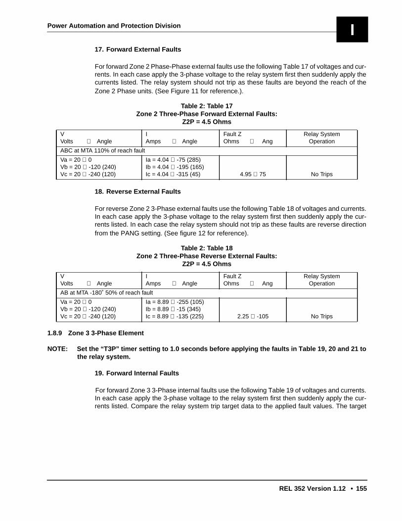
Power Automation and Protection Division
REL 352 Version 1.12 • 155
I17. Forward External Faults
For forward Zone 2 Phase-Phase external faults use the following Table 17 of voltages and cur-rents. In each case apply the 3-phase voltage to the relay system first then suddenly apply thecurrents listed. The relay system should not trip as these faults are beyond the reach of theZone 2 Phase units. (See Figure 11 for reference.).
18. Reverse External Faults
For reverse Zone 2 3-Phase external faults use the following Table 18 of voltages and currents.In each case apply the 3-phase voltage to the relay system first then suddenly apply the cur-rents listed. In each case the relay system should not trip as these faults are reverse directionfrom the PANG setting. (See figure 12 for reference).
1.8.9 Zone 3 3-Phase Element
NOTE: Set the “T3P” timer setting to 1.0 seconds before applying the faults in Table 19, 20 and 21 tothe relay system.
19. Forward Internal Faults
For forward Zone 3 3-Phase internal faults use the following Table 19 of voltages and currents.In each case apply the 3-phase voltage to the relay system first then suddenly apply the cur-rents listed. Compare the relay system trip target data to the applied fault values. The target
Table 2: Table 17Zone 2 Three-Phase Forward External Faults:
Z2P = 4.5 Ohms
VVolts ∠ Angle
IAmps ∠ Angle
Fault ZOhms ∠ Ang
Relay SystemOperation
ABC at MTA 110% of reach fault
Va = 20 ∠ 0Vb = 20 ∠ -120 (240)Vc = 20 ∠ -240 (120)
Ia = 4.04 ∠ -75 (285)Ib = 4.04 ∠ -195 (165)Ic = 4.04 ∠ -315 (45) 4.95 ∠ 75 No Trips
Table 2: Table 18Zone 2 Three-Phase Reverse External Faults:
Z2P = 4.5 Ohms
VVolts ∠ Angle
IAmps ∠ Angle
Fault ZOhms ∠ Ang
Relay SystemOperation
AB at MTA -180˚ 50% of reach fault
Va = 20 ∠ 0Vb = 20 ∠ -120 (240)Vc = 20 ∠ -240 (120)
Ia = 8.89 ∠ -255 (105)Ib = 8.89 ∠ -15 (345)Ic = 8.89 ∠ -135 (225) 2.25 ∠ -105 No Trips

I.L. 40-201.9B Power Automation and Protection Division
156 • REL 352 Version 1.12
data should be within +/- 10% on magnitude and +/- 3 degrees on phase. Trip time should fallwithin 1.00 - 1.05 seconds (Refer to figure 7 for reference).
20. Forward External Faults
For forward Zone 3 3-Phase external faults use the following Table 20 of voltages and currents.In each case apply the 3-phase voltage to the relay system first then suddenly apply the cur-rents listed. The relay system should not trip as these faults are beyond the reach of the Zone3 3-phase unit. (Refer to figure 8 for reference).
21. Reverse External Faults
For reverse Zone 3 3-Phase external faults use the following Table 21 of voltages and currents.In each case apply the 3-phase voltage to the relay system first then suddenly apply the cur-
Table 2: Table 19Zone 3 Three-Phase Forward Internal Faults:
Z3P = 7.0 Ohms
VVolts ∠ Angle
IAmps ∠ Angle
Fault ZOhms ∠ Ang
Relay SystemOperation
ABC at MTA 90% of reach fault
Va = 20 ∠ 0Vb = 20 ∠ -120 (240)Vc = 20 ∠ -240 (120)
Ia = 3.17 ∠ -75 (285)Ib = 3.17 ∠ -195 (165)Ic = 3.17 ∠ -315 (45) 6.3 ∠ 75
Z3T TripFault type ABCZ3P UnitTrip time 1.0 - 1.05 mS
Table 2: Table 20Zone 3 Three-Phase Forward External Faults:
Z3P = 7.0 Ohms
VVolts ∠ Angle
IAmps ∠ Angle
Fault ZOhms ∠ Ang
Relay SystemOperation
ABC at MTA 110% of reach fault
Va = 20 ∠ 0Vb = 20 ∠ -120 (240)Vc = 20 ∠ -240 (120)
Ia = 2.6 ∠ -75 (285)Ib = 2.6 ∠ -195 (165)Ic = 2.6 ∠ -315 (45) 7.7 ∠ 75 No Trips

Power Automation and Protection Division
REL 352 Version 1.12 • 157
Irents listed. In each case the relay system should not trip as these faults are reverse directionfrom the PANG setting (refer to figure 9).
WARNING
The user should verify that Standing Relay Trip SRT = NO in the Test Mode Function (SeeSection 4.4.5, on page 45) prior to putting the REL 350 in service.
1.9 Out of Step System Functional Tests
For systems equipped with OST logic the following settings may be used to check the OST logic inREL 350:
The situation is described more accurately in the sketch of Figure 3-14, on page 34.
NOTE: These tests are optional and require programing Computer Aided, Multi-amp or Doble testequipment.
Table 2: Table 21Zone 3 Three-Phase Reverse External Faults:
Z3P = 7.0 Ohms
VVolts ∠ Angle
IAmps ∠ Angle
Fault ZOhms ∠ Ang
Relay SystemOperation
ABC at MTA -180˚ 50% of reach fault
Va = 20 ∠ 0Vb = 20 ∠ -120 (240)Vc = 20 ∠ -240 (120)
Ia = 5.71 ∠ -255 (105)Ib = 5.71 ∠ -15 (345)Ic = 5.71 ∠ -135 (225)) 3.5 ∠ -105 No Trips
PANG = 65GANG = 65ZR = 3.0BKUP = OUTLOPB = NOFDOP = INFDOG = INDIRU = ZSEQIOM = 0.5TOG = BLKZ2P = 8.5T2P = 0.1Z2GF = 6.5Z2GR = 0.01
T2G = 0.1Z3P = 11.0T3P = .2Z3GF = 11.0Z3GR = 0.01T3G = .2OST = WAYOOSB = BOTHRT = 2.0RU = 4.0OST1 = 2OST2 = 3OST3 = 3OSOT = 100
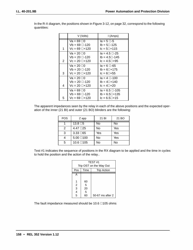
I.L. 40-201.9B Power Automation and Protection Division
158 • REL 352 Version 1.12
In the R-X diagram, the positions shown in Figure 3-12, on page 32, correspond to the followingquantities:
The apparent impedances seen by the relay in each of the above positions and the expected oper-ation of the inner (21 BI) and outer (21 BO) blinders are the following:
Test #1 indicates the sequence of positions in the RX diagram to be applied and the time in cyclesto hold the position and the action of the relay..
The fault impedance measured should be 10.6 ∠105 ohms
V (Volts) I (Amps)
1
Va = 69 ∠0Vb = 69 ∠-120Vc = 69 ∠+120
Ia = 5 ∠-5Ib = 5∠-125Ic = 5∠+115
2
Va = 20 ∠0Vb = 20 ∠-120Vc = 20 ∠+120
Ia = 4.5 ∠-25Ib = 4.5∠-145Ic = 4.5∠+95
3
Va = 20 ∠0Vb = 20 ∠-120Vc = 20 ∠+120
Ia = 6 ∠-65Ib = 6∠+175Ic = 6∠+55
4
Va = 20 ∠0Vb = 20 ∠-120Vc = 20 ∠+120
Ia = 4 ∠-100Ib = 4∠+140Ic = 4∠+20
5
Va = 69 ∠0Vb = 69 ∠-120Vc = 69 ∠+120
Ia = 6.5 ∠-105Ib = 6.5∠+135Ic = 6.5∠+15
POS Z app 21 BI 21 BO
1 13.8 ∠5 No No
2 4.47 ∠25 No Yes
3 3.33 ∠65 Yes Yes
4 5.00 ∠100 No Yes
5 10.6 ∠105 No No
TEST #1Trip OST on the Way Out
Pos Time Trip Action
A
12345
60520560 50-67 ms after 2

Power Automation and Protection Division
REL 352 Version 1.12 • 159
I
WARNING
The user should verity that Standing Relay Trip SRT = NO in the Test Mode Function (seeSection 4.4.5, on page 45) prior to putting the REL 352 in service.

I.L. 40-201.9B Power Automation and Protection Division
160 • REL 352 Version 1.12
THIS PAGE RESERVED FOR NOTES
Power Automation and Protection Division
REL 352 Version 1.12 • 161
J
COMPUTER COMMUNICATIONS
1. COMMUNICATION PORT(S) USE
1.1. Introduction
REL 352 can be communicated with for target data, settings, etc., through the man-machine interface (MMI),The relay can also be communicated with via the communication (comm.) ports. Comm port communications,provides the user with more information than is available with the MMI. For example, all 16 targets are availableand a more friendly user interface for settings can be accessed (all settings are displayed on a single screenon the user’s PC). This section will provide the details of the comm port options, personal computer require-ments, connecting cables and all information necessary to communicate with and extract data from the relay.Additional communications details are contained in IL 40-603, (RCP) Remote Communication Program.
1.2. Communication Port Options
REL 352 is supplied with a rear communications port. If the network interface is not specified, a RS-232C (hard-ware standard) communications port is supplied. Network interface comm. port option allows the connection ofthe relay with many other devices to a 2-wire network. A detailed discussion of networking capabilities can befound in AD 40-600, Substation Control and Communications Application Guide.
RS-232C, rear comm. port is of the removable, Product Operated Network Interface (PONI) type and is avail-able in two styles. One is identified by a 25 pin (DB-25S) female connector, it is usually black and has a singledata comm. rate of 1200 bps. The second style is identified by a 9 pin (DB-9P) male connector and externallyaccessible dip switches (next to the connector) for setting the communication data rate. This port option is al-ways black in color, can be set for speeds of 300, 1200, 2400, 4800, or 9600 bps (see Table J-2) and offers anoption for IRIG-B time clock, synchronization input. The input to the IRIG-B port (on BNC Connector) can beeither RF (Radio Frequency) or Demodulated Format.
1.3. Personal Computer Requirements
Communication with the relay requires the use of Remote Communication Program (RCP) regardless of thecomm. port option. RCP is supplied by ABB Relay Division and is run on a personal computer (PC).
To run the program requires an IBM AT, PC/2 PC or true compatible with a minimum of 640 kilobytes of RAM,1 hard disk drive, a RS-232C comm. port and a video graphics adapter card. The PC must be running Version3.3, or higher, MS-DOS.
1.4. Connecting Cables
With each comm. port option the connecting cable requirement can be different. Also, connecting directly to aPC or connecting to a modem, for remote communication, affects the connecting cable requirements. Table J-1 provides a summary of a plug pin assignments, pins required and cable connectors.
Some terminology will be defined to aid the user in understanding cable requirements in Table J-1. Reference,is often made to the “RS-232C” standard, for data communication. The RS-232C standard describes mechan-ical, electrical, and functional characteristics. This standard is published by the Electronics Industry Association(EIA) and use of the standard is voluntary but widely accepted for electronic data transfer. ABB relay commu-nications follows the RS-232C standard for non-network data communication.

I.L. 40-201.9B Power Automation and Protection Division
162 • REL 352 Version 1.12
Although the RS-232C standard does not specify a connector shape, the most commonly used is the “D” shapeconnector. As stated in Section J.1.2 above, all ABB relay communication connectors are of the “D” shape (suchas DB-25S).
Data communication devices are categorized as either Data Terminal Equipment (DTE) or Data CommunicationEquipment (DCE). A DTE is any digital device that transmits and/or receives data and uses communicationsequipment for the data transfer. DCE’s are connected to a communication line (usually a telephone line) for thepurpose of transferring data from one point to another. In addition to transferring the data, DCE devices are de-signed to establish, maintain, and terminate the connection. As examples, a computer is a DTE device and amodem is a DCE device.
By definition the connector of a DCE is always female (usually DB-9S or 25S). Similarly, DTEs are always male(usually DB-9P or 25P). These definitions apply to the equipment being connected and to the connectors on theinterconnecting cables.
One additional piece of hardware that is required, in some applications, is a “null” modem. Null modem’s func-tion is to connect the transmit line (TXD), pin 2 by RS-232C standard, to the receive line (RXD), pin 3. A nullmodem is required when connecting like devices. That is DTE to DTE or DCE to DCE. A DCE to DCE, example,where a null modem is required, is the connection of a 25 pin, PONI to a modem.
A null modem function can be accomplished in the connecting cable or by separate null modem package. Thatis, by using a conventional RS-232C cable plus a null modem. One type of null modem, available from electron-ics suppliers, is B & B Electronics Type 232MFNM.
1.5. Setting Change Permission and Relay Password
To gain access to certain communication port functions, the REL 352 must have the remote setting capabilitypermission SETR set to YES and knowledge of the relay password is required. All communications port func-tions listed below require SETR set to YES before the actions can be performed:
Update/Change SettingsEnable Local Settings (capability)Disable Local Settings (capability)Activate Output Relays (contact testing function)
Access control, both setting permission and password knowledge is required for all communication port options.
Before attempting any of the above functions, the setting of SETR must be verified via the front panel MMI. Us-ing the setting change procedure in Section 4, subsection 4.1 (page 39), verify or change SETR such that it isset to YES.
Using comm. port communications, the ability to change settings from the MMI can be disabled.The RCP, Pass-word Menu Choice “Disable Local Settings” when selected, will block setting changes via the MMI. Blocking thefront panel setting changes, may be useful for situations in which the access to the relay cannot be secured fromtampering by unauthorized persons.
Password:
When the REL 352 is received from the factory or if the user loses the relay password, a new password can beassigned with the following procedure:
Turn off the relay dc supply voltage for a few seconds,Restore the dc supply voltage and wait for the relay to complete the self check/start-up routine,Using RCP, perform the Password Menu choice “Set Relay Password”,Use the word “password” when prompted for the “current relay password” andThen enter a new password.

Power Automation and Protection Division
REL 352 Version 1.12 • 163
JPassword setting change procedure must be completed within 15 minutes of energizing relay or “pass-word” will not be accepted as the “current” password.
1.6. Troubleshooting
In the event the communication remains unsuccessful, first make sure that the relay is powered, proper com-munication cable is used (Table J-1, below), and the connection is good.
For further testing, check that the bit rate (Baud) on the RS-PONI (Table J-2, page 164) is set to correspond tothe one displayed at the bottom right of the RCP display.
If after these verifications the problem remains, try to remove the power from the relay and apply it again. If thecommunication still fails (several attempts), the communication equipment needs to be serviced.
1.7. SIXTEEN FAULT TARGET DATA
The REL 352 saves the latest 16 fault records, but only the latest two fault records can be accessed from thefront panel. For complete 16 fault data, the computer communication is necessary..
* NOTE: A communications cable kit item identification number 1504B78G01) that will accommodatemost connection combinations is available through your local ABB representative.
Table J-1 Communications Cable Requirements
Connection TypeCable
(Straight = nonull modem)
Pins Req’d.(All pins
not required)Cable Connectors Data Rate
DB-25S, RS-232C connected to PC* Straight 2, 3, 7To port: 25 pin DTETo PC: 9 or 25 pin DCE
1200 bps only
DB-25S, RS-232C connected to modem Null Modem 2, 3, 7To port: 25 pin DTEto Modem: 25 pin DTE
1200 bps only
DB-9P, RS-232C connected to PC* Null Modem 2, 3, 5To port: 9 pin DCETo PC: 9 or 25 pin DCE
See Table J-2For settings
DB-9P, RS-232C connected to modem*Straight
2, 3, 5To port: 9 pin DCETo Modem: 25 pin DTE
See Table J-2For settings
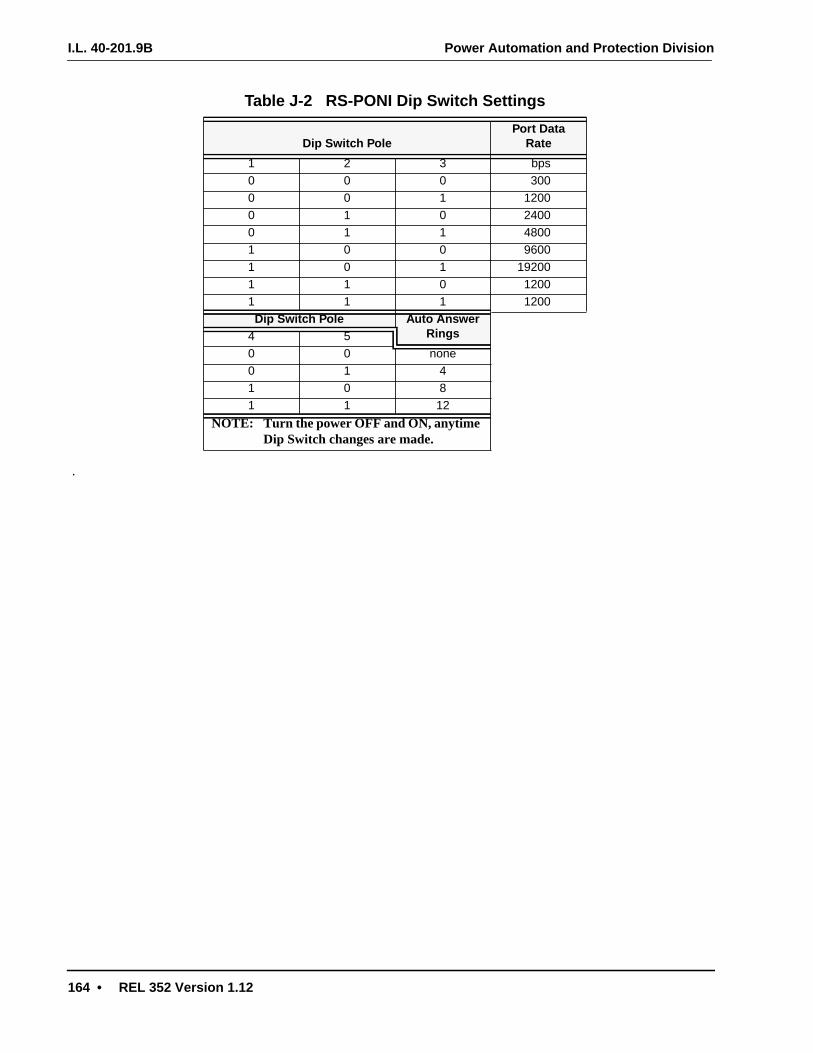
I.L. 40-201.9B Power Automation and Protection Division
164 • REL 352 Version 1.12
.
Table J-2 RS-PONI Dip Switch Settings
Dip Switch PolePort Data
Rate
1 2 3 bps0 0 0 3000 0 1 12000 1 0 24000 1 1 48001 0 0 96001 0 1 192001 1 0 12001 1 1 1200Dip Switch Pole Auto Answer
Rings4 50 0 none0 1 41 0 81 1 12
NOTE: Turn the power OFF and ON, anytimeDip Switch changes are made.

Power Automation and Protection Division
REL 352 Version 1.12 • 165
K
APPLICATION NOTES
1. COMMUNICATION EQUIPMENT INTERFACE
1.1 “Quiescent” Mode of Operation of FSK Data Communication Equipment.
Frequency shift (FSK) DCE (Data Communication Equipment) shifts carrier frequency in re-sponse to the modulating signal IKEY.
Under certain conditions (i.e. to prevent PLC from interfering with other communication equip-ment) it is necessary to prevent continuous frequency shift under normal load condition. Theconstant frequency, present on the line will be that corresponding to SPACE (IKEY=0).
The frequency shift must be, of course, resumed during system faults.
As explained in sections 3 and 5 there are two ways of achieving this goal:
• Setting IKEY above line load
• Setting C1 - (positive sequence coefficient) low enough to reduce the contribution ofload to combined-sequence output IT
Please remember that:
IT = -C1I1 + C2I2 + C0I0
The user must be aware that this approach, while eliminating the line load, also makesthe protection system less sensitive to balanced three-phase faults .
2. PHASE COMPARISON SIGNAL POLARITY CONSIDERATIONS
The REL 352 relay system phase comparison logic requires proper polarity of the comparisonsignals to be maintained. Since many different types of communications equipment can beused with this relay system, careful consideration of overall signal throughput polarity is of ut-most importance. The REL 352 interconnect module provides six polarity jumpers to allowproper interface with any type of communication equipment by allowing for polarity adjustmentson signals MARK1, SPACE1,MARK2, SPACE2, KEY OUT, and CHAN FAIL if needed. Theoverall polarity conventions must be maintained from end to end between two line terminals forproper phase comparison as described below.
2.1 REL 352 Signal Polarity Convention with 2-State “ON / OFF” PLC applications(COMM setting = 2ST)
When the REMOTE REL 352 microprocessor logic outputs a logic “0” on the IKEY output(interconnect module connector J5 pin C23), the LOCAL received SPACE1 input andSPACE2 input if used (interconnect module J5 pin A28 /TP5 and pin A27/TP3 respective-ly) MUST be a logic “1” state.
Conversely, When the REMOTE REL 352 microprocessor logic outputs a logic “1” onthe IKEY output (interconnect module connector J5 pin C23), the LOCAL receivedSPACE1 input and Space 2 input if used (interconnect module J5 pin A28 /TP5 and pinA27/TP3 respectively) MUST be a logic “0” state.

I.L. 40-201.9B Power Automation and Protection Division
166 • REL 352 Version 1.12
Typically with a “ON / OFF” PLC, the receiver output is a logic “1” when the remote transmitteris keyed with a logic “1”. The following procedure will achieve the above throughput polarityconvention with this type of communications equipment:
1. Connect the relay system's XMTR KEY output (REL 352 Rear Panel, TB4 Terminals 12 &13) to the “CARRIER START”, “CARRIER KEY”, or “KEY” input on the “ON / OFF” PLC set.
This is the standard method of keying the PLC.
2. Set the REL 352's KEY OUT polarity jumper (interconnect module - JMP6) to “Normal” (po-sition 2-3).
This will cause the transmitter to be keyed “ON” whenever the IKEY signal generated bythe relay system is a logic “1” state.
3. Connect the “ON / OFF” PLC's “Receiver Output” to the SPACE1 (and SPACE2 for 3-Ter-minal applications) inputs to the rear panel of the relay system (TB5 Terminals 7 & 10, TB5Terminal 11 & 14 respectively).
Only the SPACE input(s) are used since phase comparison only occurs during negativehalf-cycles of the system power waveform for “ON / OFF” PLC applications. The relay sys-tem's MARK inputs are deactivated in this case.
4. Set the REL 352's SPACE1 (and SPACE2 for 3-Terminal applications) polarity jumpers (in-terconnect module - JMP5 and JMP3 respectively) to “Normal” (position 2-3).
Even though the “ON / OFF” PLC's receiver output presents a logic “1” to the rear panelSPACE inputs of the REL 352 when the remote transmitter is keyed “ON”, there is an inter-nal signal inversion in the opto-isolated input circuitry (optoisolated input module U3 andU6) which inverts the logic “1” to a logic “0” before inputting into the microprocessor's logic.Thus, the local REL 352's SPACE1 (and SPACE2) inputs, as seen by the microprocessor,(interconnect module TP5 and TP3) receive a logic “0” state whenever the remote transmit-ter is keyed per the prescribed polarity convention.
NOTE: If the communications equipment to be employed has an unusual receiver out-put stage which is logic “0” when the remote transmitter is keyed, disregardthe polarity jumper settings mentioned in step 4 above and instead set bothJMP 5 and JMP3 to “Inverted” (position 1-2) instead.
5. If the EXT. CHAN FAILURE function is not used, and therefore nothing is connected to ei-ther of the CHAN FAIL1 or CHAN FAIL2 inputs on the rear of the REL 352, then make sureto set the CHAN FAIL polarity jumper (interconnect module JMP1) to “Normal” (position 2-3). Otherwise, the relay system will permanently have the EXT CHANNEL FAILURE func-tion activated which effectively disables the primary phase comparison protection function.
If an external channel failure device (i.e. Checkback) is to be used be aware that the EXT.CHAN FAIL function is active whenever a logic “1” voltage is input the to EITHER of theCHAN FAIL1 or CHAN FAIL2 inputs at the rear of the REL 352 (TB5 terminals 9&10 and13&14 respectively) WHEN the CHAN FAIL polarity jumper on the relay (interconnect mod-ule JMP1) is set to “Normal” (2-3) position.
If the CHAN FAIL (interconnect module JMP1) jumper is set to “Inverted” (position 1-2),then BOTH of the CHAN FAIL inputs on the rear of the REL352 must have no voltage ap-plied (Logic “0”) to activate the EXT. CHAN FAIL function.
2.2 REL 352 Signal Polarity Convention with 3-State “FSK” PLC applications (COMM setting = 3ST)
When the REMOTE REL 352 microprocessor logic outputs a logic “0” on the IKEY out-put (interconnect module connector J5 pin C23), the LOCAL received SPACE1 input and
Power Automation and Protection Division
REL 352 Version 1.12 • 167
KSPACE2 input when used (interconnect module J5 pin A28 /TP5 and pin A27/TP3 respec-tively) MUST be a logic “1” state. Simultaneously, the LOCAL received MARK1 input andMARK2 input when used (interconnect module J5 pin C28/TP4 and pin C27/TP2 respec-tively) MUST be a logic “0” state.
Conversely, when the REMOTE REL 352 microprocessor logic outputs a logic “1” on theIKEY output (interconnect module connector J5 pin C23), the LOCAL received SPACE1input and SPACE2 input when used (interconnect module J5 pin A28 /TP5 and pin A27/TP3 respectively) MUST be a logic “0” state. Simultaneously, the LOCAL receivedMARK1 input and MARK2 input when used (interconnect module J5 pin C28/TP4 and pinC27/TP2 respectively) MUST be a logic “1” state.
Typically with a “FSK” PLC, the receiver's MARK/(TRIP POS.) output is a logic “1” and theSPACE/(TRIP NEG.) output is a logic “0” when the remote transmitter is keyed with a logic “1”.The following procedure will achieve the above throughput polarity convention with this type ofcommunications equipment:
1. Connect the relay system's XMTR KEY output (REL 352 Rear Panel, TB4 Terminals 12 &13) to the “PC KEY”, or “KEY” input on the “FSK” PLC set.
This is the standard method of keying the PLC.
2. Set the REL 352's KEY OUT polarity jumper (interconnect module - JMP6) to “Normal” (po-sition 2-3). This will cause the transmitter to be keyed (frequency shifted, typically “SHIFTLO”) whenever the IKEY signal generated by the relay system is a logic “1” state.
3. Connect the “FSK” PLC's receiver's SPACE/(TRIP NEG) output to the REL 352's SPACE1(and SPACE2 for 3- Terminal applications) inputs on the rear panel of the relay system(TB5 Terminals 7 & 10, TB5 Terminal 11 & 14 respectively).
4. Connect the “FSK” PLC's receiver's MARK/(TRIP POS) output to the REL 352's MARK1(and MARK2 for 3- Terminal applications) inputs on the rear panel of the relay system (TB5Terminals 8 & 10, TB5 Terminal 12 & 14 respectively).
This is the standard method of connecting the SPACE/(TRIP NEG) and MARK/(TRIP POS)signals.
5. Set the REL 352's SPACE1, SPACE2 (when used), MARK 1, MARK2 (when used) polarityjumpers (interconnect module - JMP5, JMP3, JMP4, JMP2 respectively) to “Inverted” (po-sition 1-2).
Even though the “FSK” PLC's receiver output presents a logic “0” to the rear panel SPACEinputs and a logic “1” to the rear panel MARK inputs of the REL 352 when the remote trans-mitter is keyed “ON”, there is an internal signal inversion in the opto-isolated input circuitry(optoisolated input module I.Cs U2,U3,U5 and U6) which inverts the signals before input-ting into the microprocessor's logic. Thus, the local REL 352's SPACE and MARK inputs,as seen by the microprocessor, are receiving the signals in reverse polarity. By setting allfour of the SPACE & MARK polarity jumpers to the “inverted” position, the correct polaritiesare restored.
NOTE: If the communications equipment to be employed has an unusual receiver out-put stage which has a logic “1” on the SPACE/(TRIP NEG.) output and a logic“0” on the MARK/(TRIP POS.) when the remote transmitter is keyed with a logic“1”, disregard the polarity jumper settings mentioned in step 4 above and in-stead set jumpers JMP5, JMP3, JMP4, and JMP2 to the “Normal” (position 2-3)instead.
I.L. 40-201.9B Power Automation and Protection Division
168 • REL 352 Version 1.12
6. If the EXT. CHAN FAILURE function is not used, and therefore nothing is connected to ei-ther of the CHAN FAIL1 or CHAN FAIL2 inputs on the rear of the REL 352, then make sureto set the CHAN FAIL polarity jumper (interconnect module JMP1) to “Normal” (position 2-3). Otherwise, the relay system will permanently have the EXT CHANNEL FAILURE func-tion activated which effectively disables the primary phase comparison protection function.
7. If an external channel failure device (i.e. Checkback) is to be used be aware that the EXT.CHAN FAIL function is active whenever a logic “1” voltage is input the to EITHER of theCHAN FAIL1 or CHAN FAIL2 inputs at the rear of the REL 352 (TB5 terminals 9&10 and13&14 respectively) WHEN the CHAN FAIL polarity jumper on the relay (interconnect mod-ule JMP1) is set to “Normal” (2-3) position.
8. If the CHAN FAIL (interconnect module JMP1) jumper is set to “Inverted” (position 1-2),then BOTH of the CHAN FAIL inputs on the rear of the REL352 must have no voltage ap-plied (Logic “0”) to activate the EXT. CHAN FAIL function.
3. SQUARE WAVE DURATION
The duration of square waves used for phase comparison depends on the magnitude of IT andthe levels of KEY, LP and LN settings. The following two figures (figure K-1 (page 169), 60 Hz,figure K-2 (page 170), 50 Hz) provide duration of square wave as the function of ratio of IKEYsetting and IT [rms].
Please note that the information applies to LP and LN as well.
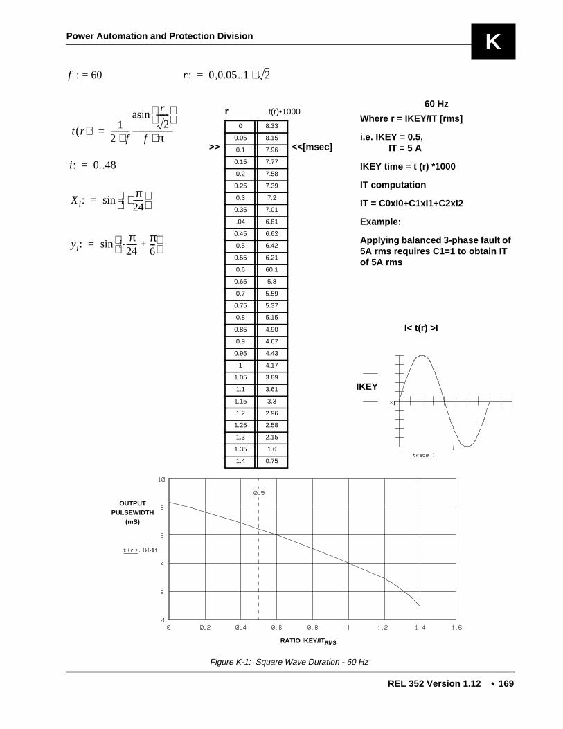
Power Automation and Protection Division
REL 352 Version 1.12 • 169
K
IKEY
i
i
60 Hz
Where r = IKEY/IT [rms]
i.e. IKEY = 0.5,IT = 5 A
IKEY time = t (r) *1000
IT computation
IT = C0xI0+C1xI1+C2xI2
Example:
Applying balanced 3-phase fault of5A rms requires C1=1 to obtain ITof 5A rms
I< t(r) >I
f : = 60 r : 0 0.05..1 2⋅,=
t r( ): 12 f⋅----------
r
2-------
asin
f π⋅----------------------=
i : 0..48=
Xi : iπ24------⋅
sin=
yi : i .π24------ π
6---+
sin=
r t(r)•1000
0 8.33
0.05 8.15
0.1 7.96
0.15 7.77
0.2 7.58
0.25 7.39
0.3 7.2
0.35 7.01
.04 6.81
0.45 6.62
0.5 6.42
0.55 6.21
0.6 60.1
0.65 5.8
0.7 5.59
0.75 5.37
0.8 5.15
0.85 4.90
0.9 4.67
0.95 4.43
1 4.17
1.05 3.89
1.1 3.61
1.15 3.3
1.2 2.96
1.25 2.58
1.3 2.15
1.35 1.6
1.4 0.75
>> <<[msec]
OUTPUTPULSEWIDTH
(mS)
Figure K-1: Square Wave Duration - 60 Hz
RATIO IKEY/ITRMS
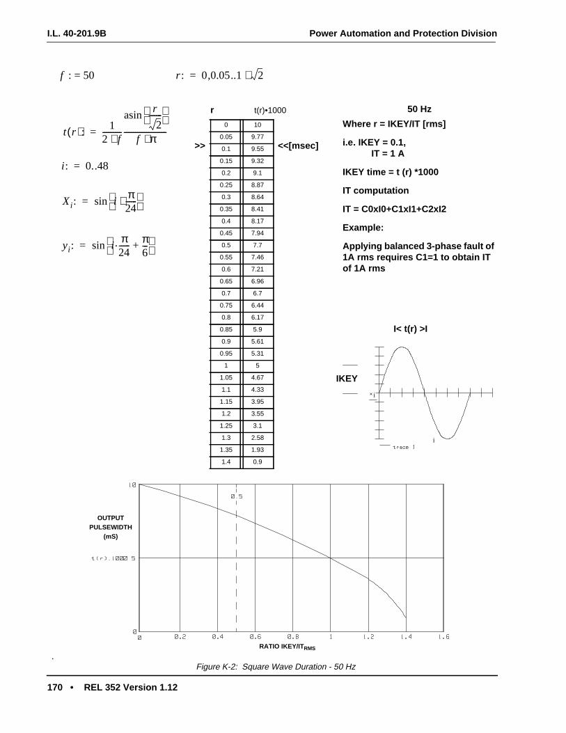
I.L. 40-201.9B Power Automation and Protection Division
170 • REL 352 Version 1.12
.
IKEY
i
i
50 Hz
Where r = IKEY/IT [rms]
i.e. IKEY = 0.1,IT = 1 A
IKEY time = t (r) *1000
IT computation
IT = C0xI0+C1xI1+C2xI2
Example:
Applying balanced 3-phase fault of1A rms requires C1=1 to obtain ITof 1A rms
I< t(r) >I
f : = 50 r : 0 0.05..1 2⋅,=
t r( ): 12 f⋅----------
r
2-------
asin
f π⋅-----------------------=
i : 0..48=
Xi : iπ24------⋅
sin=
yi : i .π24------ π
6---+
sin=
r t(r)•1000
0 10
0.05 9.77
0.1 9.55
0.15 9.32
0.2 9.1
0.25 8.87
0.3 8.64
0.35 8.41
0.4 8.17
0.45 7.94
0.5 7.7
0.55 7.46
0.6 7.21
0.65 6.96
0.7 6.7
0.75 6.44
0.8 6.17
0.85 5.9
0.9 5.61
0.95 5.31
1 5
1.05 4.67
1.1 4.33
1.15 3.95
1.2 3.55
1.25 3.1
1.3 2.58
1.35 1.93
1.4 0.9
>> <<[msec]
OUTPUTPULSEWIDTH
(mS)
RATIO IKEY/ITRMS
Figure K-2: Square Wave Duration - 50 Hz
Power Automation and Protection Division
REL 352 Version 1.12 • 171
LSYSTEM DIAGRAMS
Figure No. Description Page No.
L-1 REL 352 Block Diagram, 1618C33 172
L-2 REL 352 Power Supply Internal Schematic 1356D56 173
L-3 REL 352 System Logic Diagram 1358D80 Sh 1 174
L-4 REL 352 System Logic Diagram 1358D80 Sh 2 175

I.L. 40-201.9BP
ower A
utomation and P
rotection Division
172•
RE
L 352 Version 1.12
Figure L-1: REL 352 Block Diagram
Sub 11618C33

I.L. 40-201.9B Power Automation and Protection Division
REL 352 Version 1.12
1356D56
Native CAD
In CAD40 Directory File Available
Figure L-2: REL 352 Power Supply Internal Schematic

I.L. 40-201.9B Power Automation and Protection Division
REL 352 Version 1.12
1358D801 of 2
Native CAD
In CAD40 Directory File Available
Figure L-3: REL System Logic Diagram

I.L. 40-201.9B Power Automation and Protection Division
REL 352 Version 1.12
1358D802 of 2
Native CAD
In CAD40 Directory File Available
Figure L-4: REL System Logic Diagram


![Acceptance Test Plan[10]](https://img.pdfslide.us/doc/110x75/577cde5b1a28ab9e78aef9b8/acceptance-test-plan10.jpg)