Embed Size (px)
Citation preview
Third Generation Solar cells
Hiwa Modarresi
17th June 2009
"Energy & Nano" - Top Master Symposium in Nanoscience 20091
Outline Sunlight spectrum How a classical solar cell works First generation solar cells Second generation solar cells The main losses in solar cells Third generation solar cells
Band gap engineering Multiple exciton generation Hot carrier solar cells Up conversion Down conversion Tandem cells
Summary
"Energy & Nano" - Top Master Symposium in Nanoscience 20092
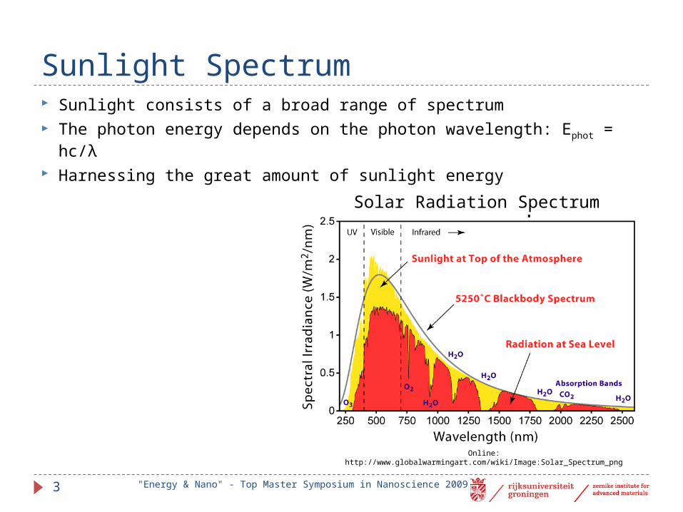
Sunlight Spectrum Sunlight consists of a broad range of spectrum The photon energy depends on the photon wavelength: Ephot = hc/λ
Harnessing the great amount of sunlight energy
"Energy & Nano" - Top Master Symposium in Nanoscience 20093
Solar Radiation Spectrum
Online: http://www.globalwarmingart.com/wiki/Image:Solar_Spectrum_png
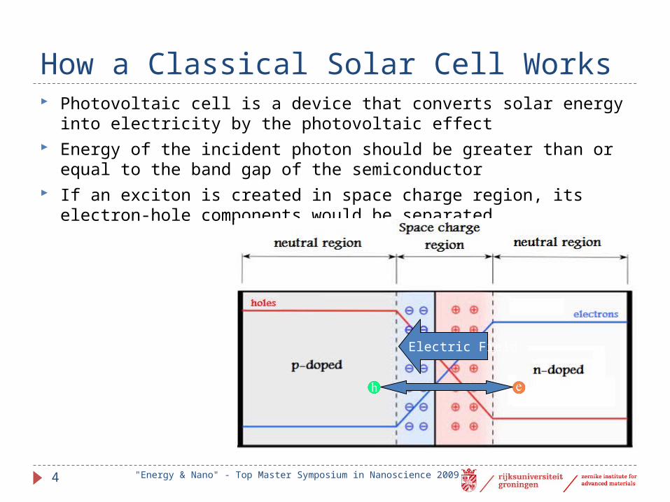
How a Classical Solar Cell Works Photovoltaic cell is a device that converts solar energy into electricity by the
photovoltaic effect Energy of the incident photon should be greater than or equal to the band
gap of the semiconductor If an exciton is created in space charge region, its electron-hole components
would be separated
Electric Field
"Energy & Nano" - Top Master Symposium in Nanoscience 20094
First Generation Solar Cells Single crystal silicon wafers Dominant in the commercial production of solar cells Consist of a large-area, single layer p-n junction Best crystalline Si solar cell efficiency: ~ 25%
Advantages Broad spectral absorption range High carrier mobility
Disadvantages Most of photon energy is wasted as heat Require expensive manufacturing technologies
"Energy & Nano" - Top Master Symposium in Nanoscience 20095
Second Generation Solar Cells Thin-film Technologies
Amorphous silicon Polycrystalline silicon Cadmium Telluride (CdTe)
Best large area Si-based solar cell efficiency: ~ 22%
Advantages Low material cost Reduced mass
Disadvantages Toxic material (Cd), Scarce material (Te)
"Energy & Nano" - Top Master Symposium in Nanoscience 20096
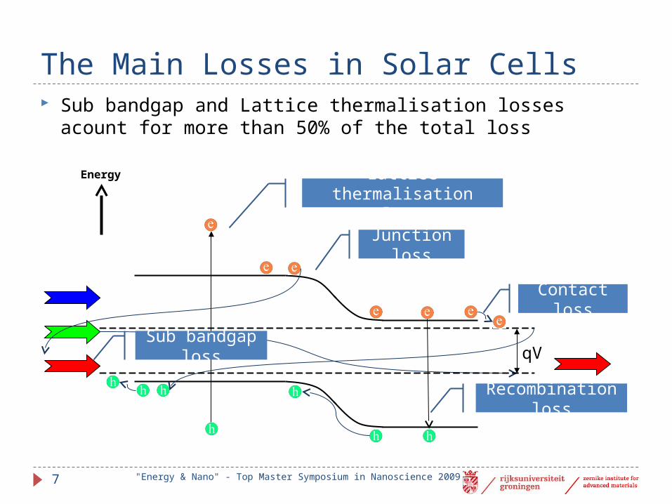
The Main Losses in Solar Cells
"Energy & Nano" - Top Master Symposium in Nanoscience 20097
qV
Lattice thermalisation loss
Junction loss
Recombination loss
Contact loss
Sub bandgap loss
Energy
Sub bandgap and Lattice thermalisation losses acount for more than 50% of the total loss
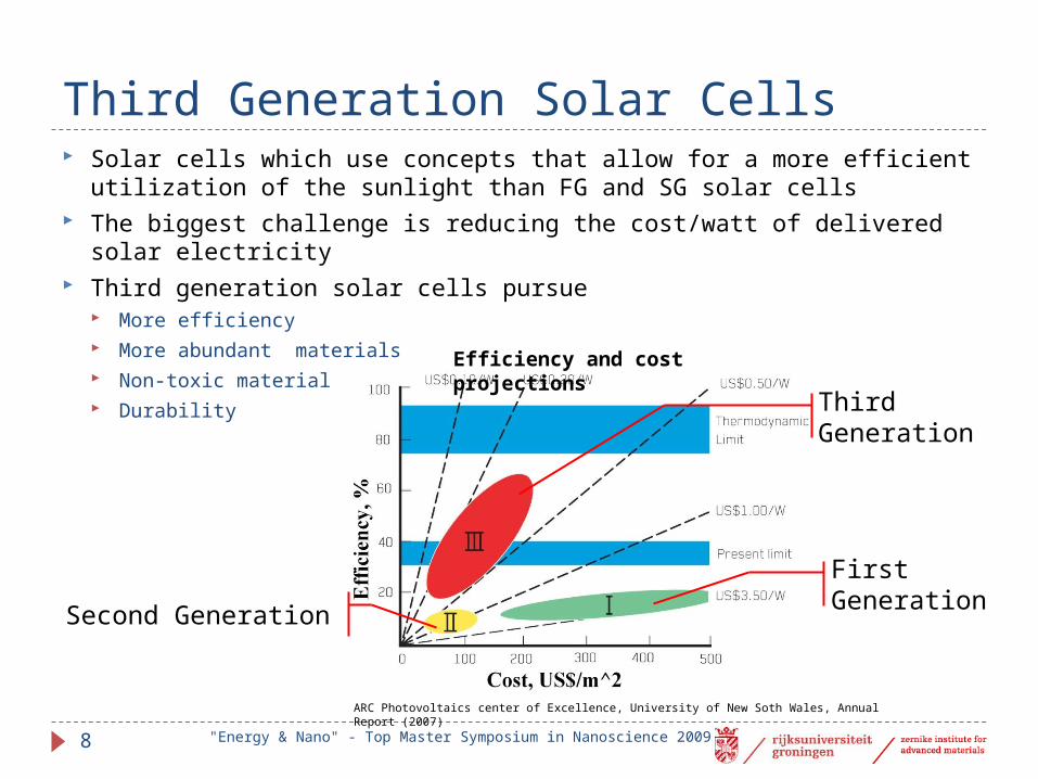
Third Generation Solar Cells Solar cells which use concepts that allow for a more efficient utilization of the
sunlight than FG and SG solar cells The biggest challenge is reducing the cost/watt of delivered solar electricity Third generation solar cells pursue
More efficiency More abundant materials Non-toxic material Durability
First Generation Second Generation
Third Generation
ARC Photovoltaics center of Excellence, University of New Soth Wales, Annual Report (2007)
Efficiency and cost projections
"Energy & Nano" - Top Master Symposium in Nanoscience 20098
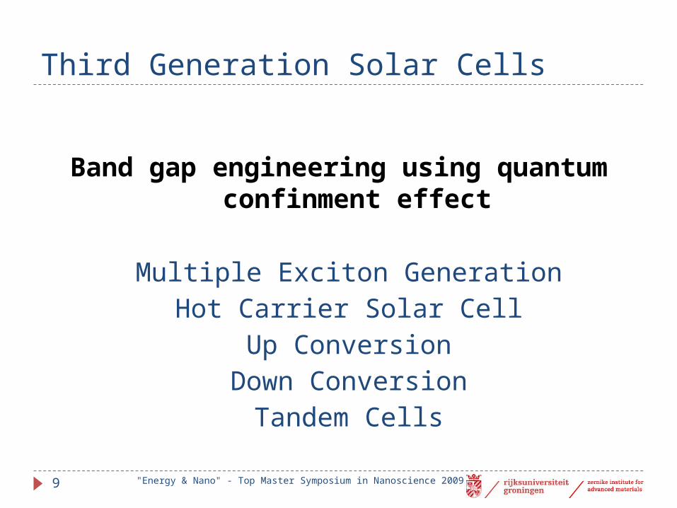
Band gap engineering using quantum confinment effect
Multiple Exciton GenerationHot Carrier Solar Cell
Up ConversionDown Conversion
Tandem Cells
Third Generation Solar Cells
"Energy & Nano" - Top Master Symposium in Nanoscience 20099
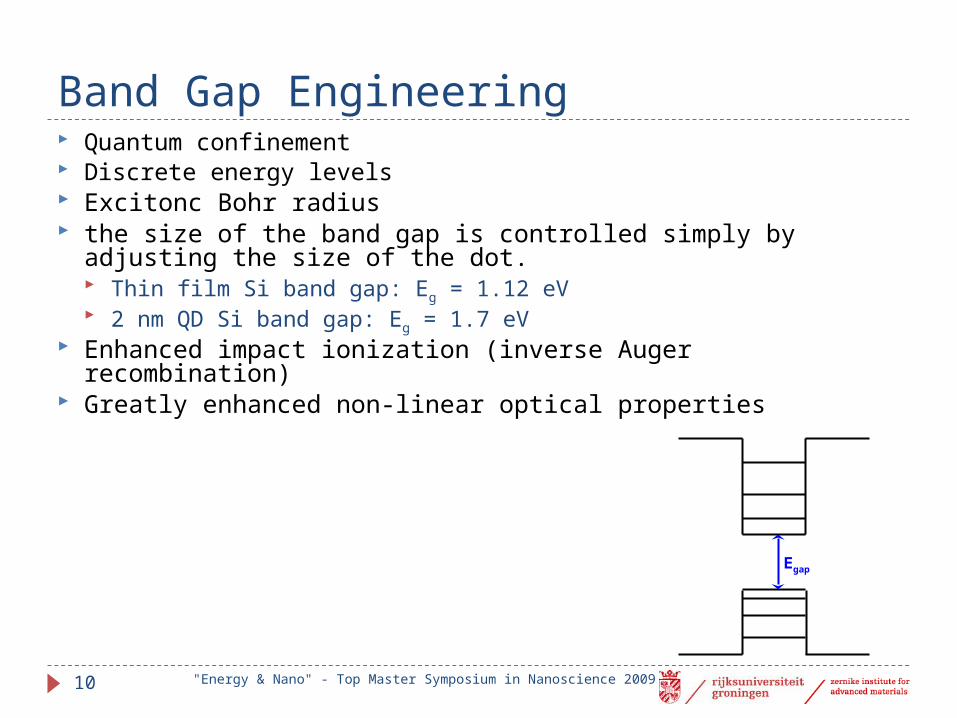
Band Gap Engineering Quantum confinement Discrete energy levels Excitonc Bohr radius the size of the band gap is controlled simply by adjusting the size of
the dot. Thin film Si band gap: Eg = 1.12 eV 2 nm QD Si band gap: Eg = 1.7 eV
Enhanced impact ionization (inverse Auger recombination) Greatly enhanced non-linear optical properties
"Energy & Nano" - Top Master Symposium in Nanoscience 200910
Egap
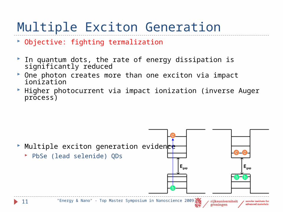
Multiple Exciton Generation Objective: fighting termalization
In quantum dots, the rate of energy dissipation is significantly reduced
One photon creates more than one exciton via impact ionization Higher photocurrent via impact ionization (inverse Auger process)
Multiple exciton generation evidence PbSe (lead selenide) QDs
"Energy & Nano" - Top Master Symposium in Nanoscience 200911
Egap Egap
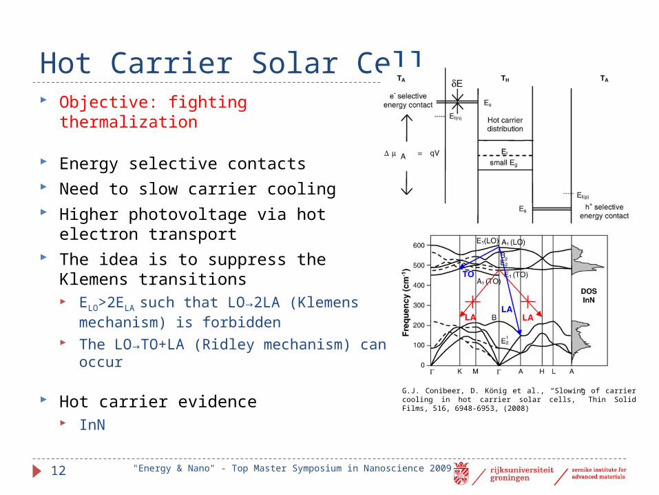
Hot Carrier Solar Cell Objective: fighting thermalization
Energy selective contacts Need to slow carrier cooling Higher photovoltage via hot electron
transport The idea is to suppress the Klemens
transitions ELO>2ELA such that LO→2LA (Klemens
mechanism) is forbidden The LO→TO+LA (Ridley mechanism) can
occur
Hot carrier evidence InN
G.J. Conibeer, D. König et al., “Slowing of carrier cooling in hot carrier solar cells,” Thin Solid Films, 516, 6948-6953, (2008)
"Energy & Nano" - Top Master Symposium in Nanoscience 200912
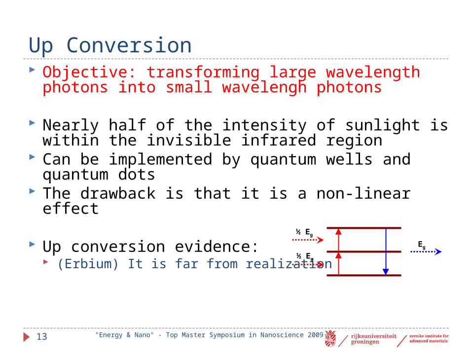
Up Conversion Objective: transforming large wavelength photons into
small wavelengh photons
Nearly half of the intensity of sunlight is within the invisible infrared region
Can be implemented by quantum wells and quantum dots The drawback is that it is a non-linear effect
Up conversion evidence: (Erbium) It is far from realization
½ Eg
½ Eg
Eg
"Energy & Nano" - Top Master Symposium in Nanoscience 200913
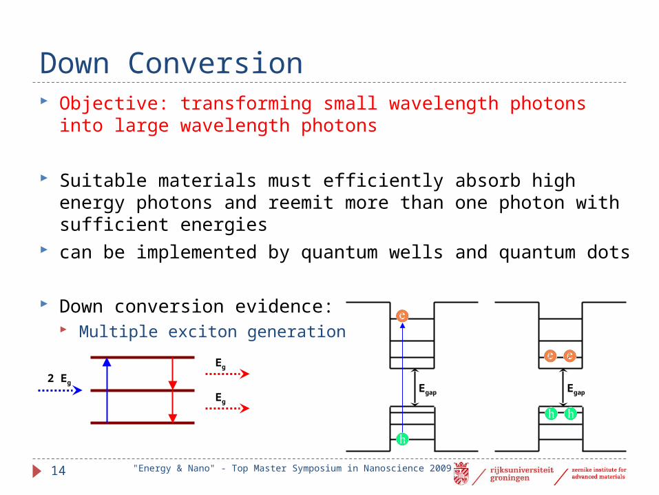
Down Conversion Objective: transforming small wavelength photons into large
wavelength photons
Suitable materials must efficiently absorb high energy photons and reemit more than one photon with sufficient energies
can be implemented by quantum wells and quantum dots
Down conversion evidence: Multiple exciton generation
Eg
Eg
2 Eg
"Energy & Nano" - Top Master Symposium in Nanoscience 200914
Egap Egap
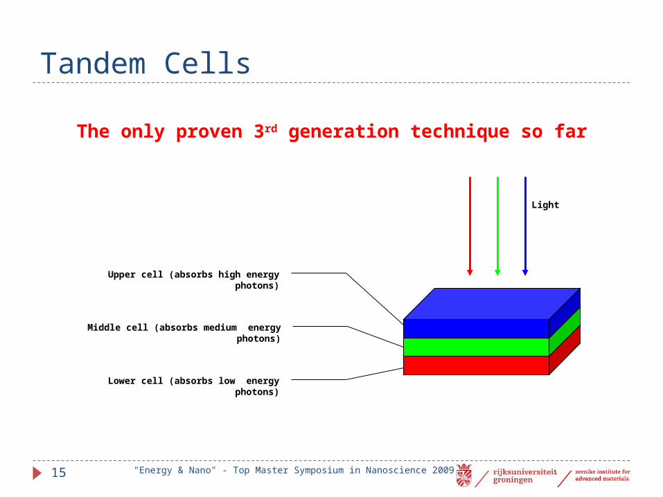
Tandem Cells
The only proven 3rd generation technique so far
Light
Upper cell (absorbs high energy photons)
Middle cell (absorbs medium energy photons)
Lower cell (absorbs low energy photons)
"Energy & Nano" - Top Master Symposium in Nanoscience 200915
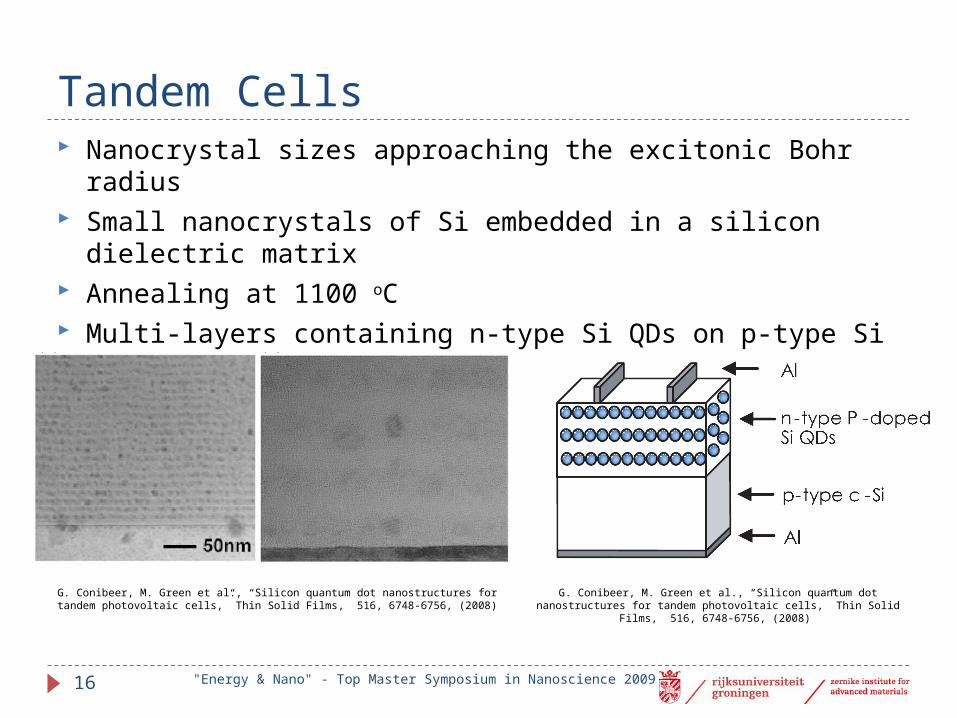
Nanocrystal sizes approaching the excitonic Bohr radius Small nanocrystals of Si embedded in a silicon dielectric matrix Annealing at 1100 oC Multi-layers containing n-type Si QDs on p-type Si wafers
Tandem Cells
"Energy & Nano" - Top Master Symposium in Nanoscience 200916
G. Conibeer, M. Green et al., “Silicon quantum dot nanostructures for tandem photovoltaic cells,” Thin Solid Films, 516, 6748-6756, (2008)
G. Conibeer, M. Green et al., “Silicon quantum dot nanostructures for tandem photovoltaic cells,” Thin Solid Films, 516, 6748-6756, (2008)
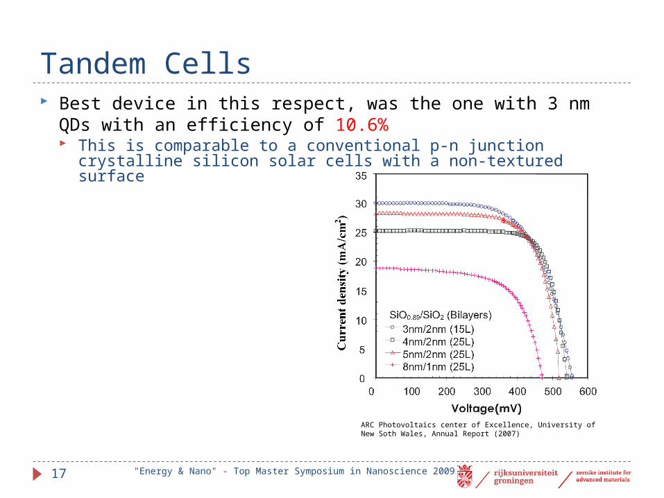
Best device in this respect, was the one with 3 nm QDs with an efficiency of 10.6% This is comparable to a conventional p-n junction crystalline silicon solar
cells with a non-textured surface
"Energy & Nano" - Top Master Symposium in Nanoscience 200917
Tandem Cells
ARC Photovoltaics center of Excellence, University of New Soth Wales, Annual Report (2007)
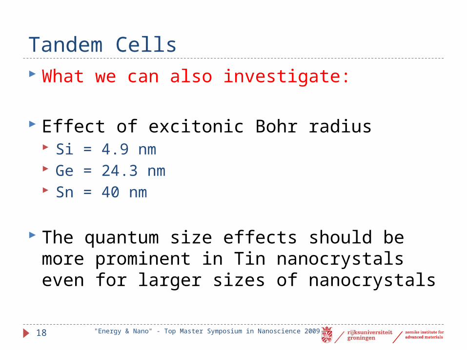
What we can also investigate:
Effect of excitonic Bohr radius Si = 4.9 nm Ge = 24.3 nm Sn = 40 nm
The quantum size effects should be more prominent in Tin nanocrystals even for larger sizes of nanocrystals
"Energy & Nano" - Top Master Symposium in Nanoscience 200918
Tandem Cells
Summary
"Energy & Nano" - Top Master Symposium in Nanoscience 200919
Objectives in third generation solar cells More efficient Less expensive Readily available Non-toxic
Quantum confinment Band gap engineering
Multiple exciton generation Already seen in QDs but with very low efficiencies
Hot carriers Far from utilization
Up conversion So far has not been realized
Down conversion Can be utilized through the concept of multiple exciton generation
Tandem cells The only proven technique in 3rd generation solar cells
Acknowledgment
I want to sincerely thank my supervisor, professor
G. Palasantzas whose kind attentions led me through the difficulties.
"Energy & Nano" - Top Master Symposium in Nanoscience 200920
THANK YOU FOR YOUR ATTENTION