Embed Size (px)
Citation preview
TFEApril 2006
1
Thin Film NewCo ASA
Presentation at
DNB NORApril 2006
TFEApril 2006
2
Talk outline
Thin Film Electronics (TFE) – Acheivements
The fundamentals of the technology
From silicon to printed electronics
Printed memory applications
Recent results
Printed memories roadmap
The market
Summary
TFEApril 2006
3
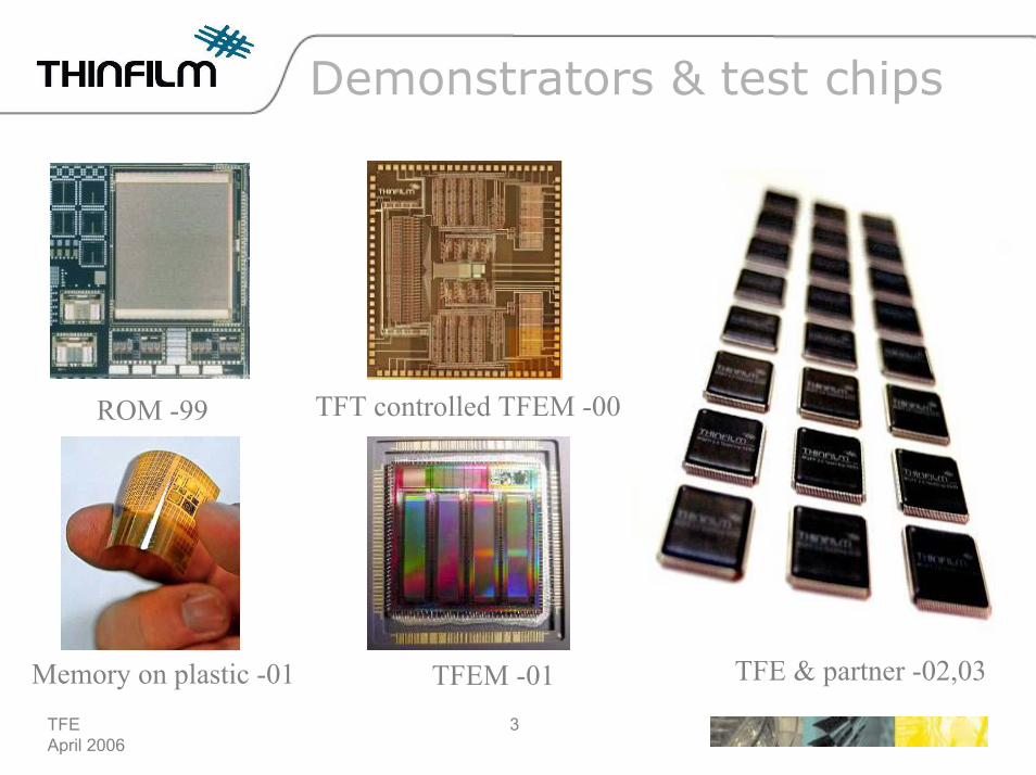
Demonstrators & test chips
TFT controlled TFEM -00ROM -99
TFE & partner -02,03Memory on plastic -01 TFEM -01
TFEApril 2006
4
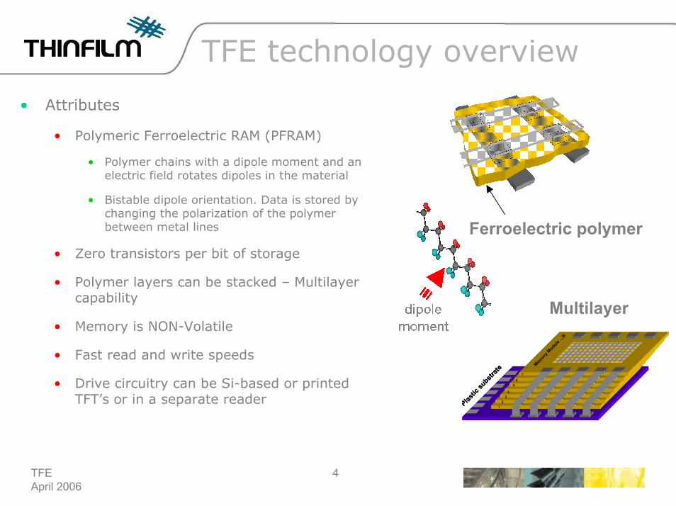
TFE technology overview
• Attributes
• Polymeric Ferroelectric RAM (PFRAM)
• Polymer chains with a dipole moment and an electric field rotates dipoles in the material
• Bistable dipole orientation. Data is stored by changing the polarization of the polymer between metal lines
• Zero transistors per bit of storage
• Polymer layers can be stacked – Multilayer capability
• Memory is NON-Volatile
• Fast read and write speeds
• Drive circuitry can be Si-based or printed TFT’s or in a separate reader
Ferroelectric polymer
Multilayer
Memory
Module ...N
12
34
56
7
Plastic
substr
ate
Memory
Module ...N
12
34
56
7
Plastic
substr
ate
TFEApril 2006
5
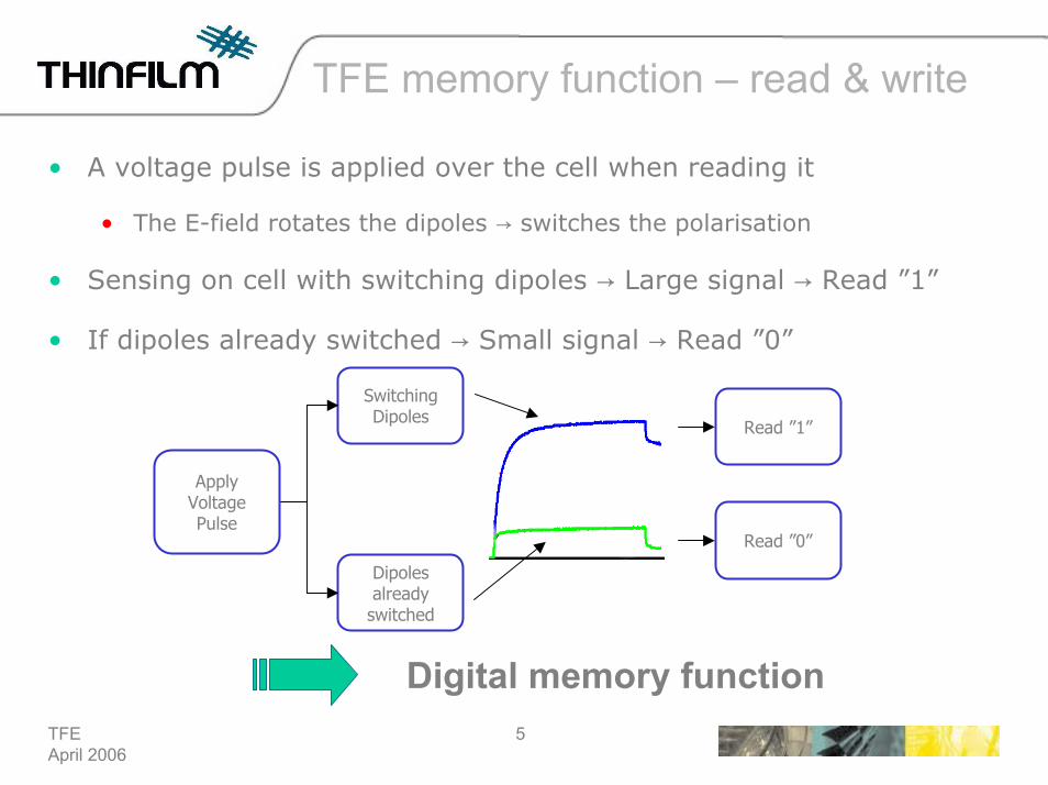
TFE memory function – read & write
• A voltage pulse is applied over the cell when reading it
• The E-field rotates the dipoles → switches the polarisation
• Sensing on cell with switching dipoles → Large signal → Read ”1”
• If dipoles already switched → Small signal → Read ”0”
SwitchingDipoles
Dipolesalready
switched
Read ”1”
Read ”0”
ApplyVoltagePulse
Digital memory function
TFEApril 2006
6
TFE technology key features
• Key Features
• Low temp solution processable - Printable (Offset, Flexo, Ink-Jet etc.)
• All included materials and substrates are based on high-volume commercial products with no or little modification
• Easy to integrate with other functionality
• Environmentally stable
• Non-toxic
• TFE Patent portfolio today, April 2006
• Patent families: 74
• Granted patents: 459 (all countries)
• Pending applications: 245
TFEApril 2006
7
From silicon to printed electronics
• Clean room environment
• Feature size: 65 – 250 nm
• Speed: 33 – 133 MHz
• Surface roughness: <10nm
• Production speed: 3.9*10-3 m2/min = 39 cm2/min = 1pc 8’’ wafer/18min
TFEApril 2006
8
From silicon to printed electronics
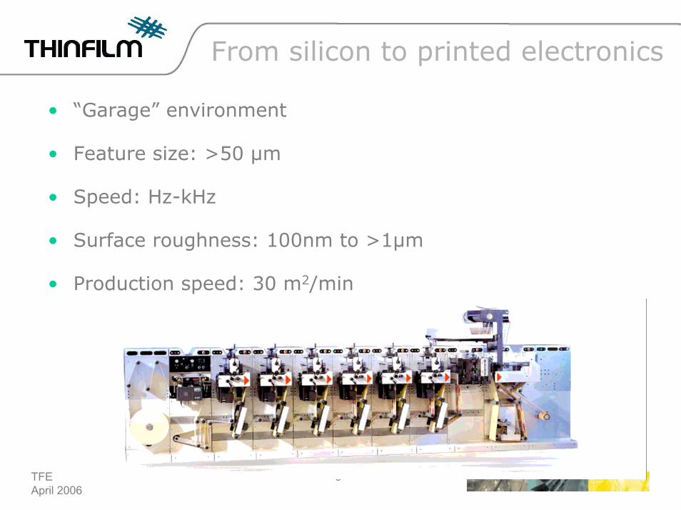
• “Garage” environment
• Feature size: >50 µm
• Speed: Hz-kHz
• Surface roughness: 100nm to >1µm
• Production speed: 30 m2/min
TFEApril 2006
9
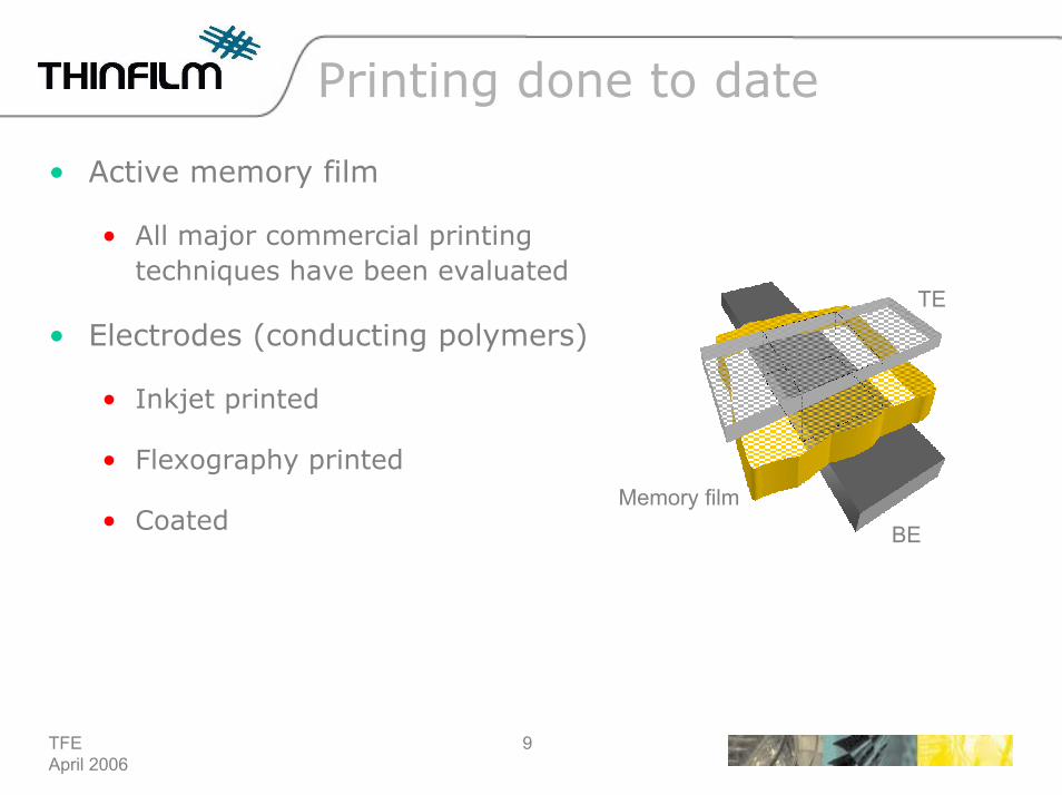
Printing done to date
• Active memory film
• All major commercial printing techniques have been evaluated
• Electrodes (conducting polymers)
• Inkjet printed
• Flexography printed
• Coated
TE
Memory filmBE
TFEApril 2006
10
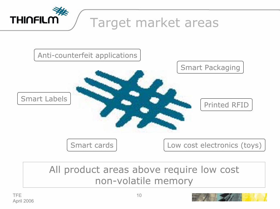
Target market areas
Smart Packaging
Smart Labels
Anti-counterfeit applications
Printed RFID
Smart cards Low cost electronics (toys)
All product areas above require low cost non-volatile memory
TFEApril 2006
11
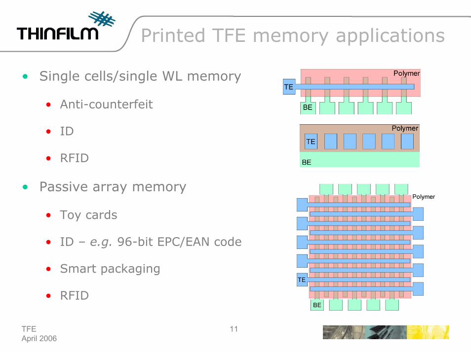
Printed TFE memory applications
• Single cells/single WL memory
• Anti-counterfeit
• ID
• RFID
• Passive array memory
• Toy cards
• ID – e.g. 96-bit EPC/EAN code
• Smart packaging
• RFID
TFEApril 2006
12
Anti-counterfeit system & method
• Unique ID – Serial number
• Static, Writeable once or Rewritable
• Added functionality to exciting anti-counterfeit techniques
• E.g. enhance holograms with added electronic functionality
• One time readable codes
• Encryption keys
• Cyclic code generation
• Unauthorised access detection
TFEApril 2006
13
Unique ID
• Unique ID on each package or even blister pack possible
• Digital ID number
• ROM – Read Only Memory
• Static number not changeable after printed on box – like EPC/EAN code
• WORM – Write Once Read Many
• Produce big batches of e.g. boxes with no ID and write the unique ID when the box has passed e.g. quality control.
• NVRAM – Non Volatile RAM – Rewriteable memory
• Update the information on the box when it goes through critical point in the production or delivery chain
TFEApril 2006
14
Unique ID - continued
• Electronic signature/pattern recognition ID
• Unique electrical properties and/or pattern on each package
• An electronic equivalent to a hologram
• Can be made extremely complicated and thereby hard to forge
• Secure ticket/entry systems
• More secure and cost less then magnetic stripes
TFEApril 2006
15
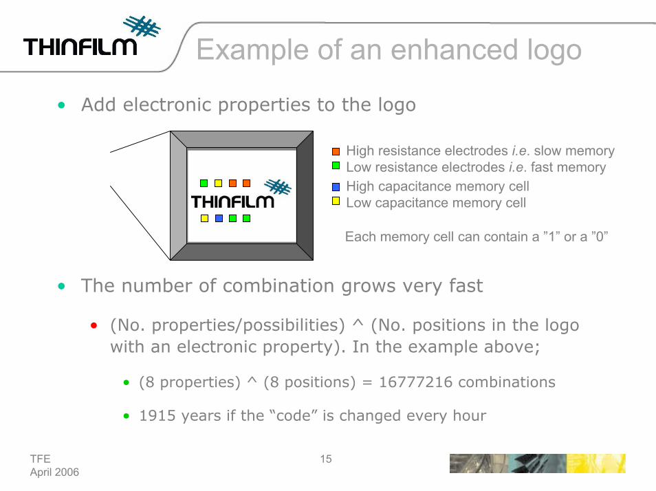
Example of an enhanced logo
• Add electronic properties to the logo
High resistance electrodes i.e. slow memory Low resistance electrodes i.e. fast memory High capacitance memory cellLow capacitance memory cell
Each memory cell can contain a ”1” or a ”0”
• The number of combination grows very fast
• (No. properties/possibilities) ^ (No. positions in the logo with an electronic property). In the example above;
• (8 properties) ^ (8 positions) = 16777216 combinations
• 1915 years if the “code” is changed every hour
TFEApril 2006
16
Usage of rewriteable memory
• One time readable codes – Destructive read
• Digital ID number that can only be read once
• Cyclic code generation
• History tracking – Shows how many times this code has been read.
• Can be used for e.g. encryption key generation
• Unwanted access detection
• Can detect if someone has tried to access the memory
TFEApril 2006
17
Printed memory in smart packages
• Information storage memory for displays, audio or other type of communication with user and/or potential customer
• Machine to package information storage in the production or the supply chain
• Now – contact interface
• Future – radio interface, RFID
TFEApril 2006
18
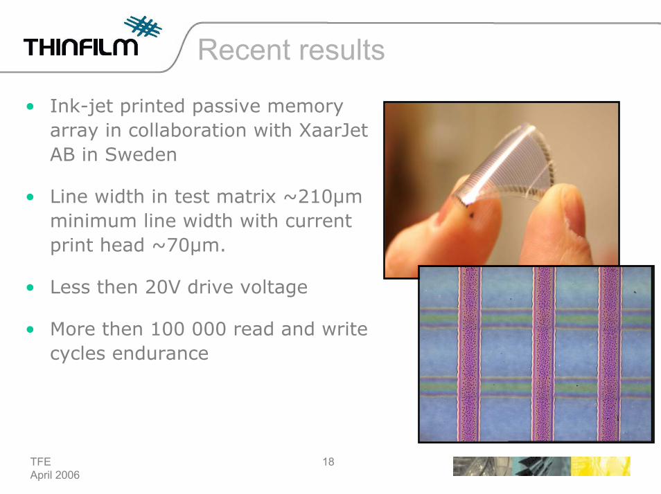
Recent results
• Ink-jet printed passive memory array in collaboration with XaarJetAB in Sweden
• Line width in test matrix ~210µm minimum line width with current print head ~70µm.
• Less then 20V drive voltage
• More then 100 000 read and write cycles endurance
TFEApril 2006
19
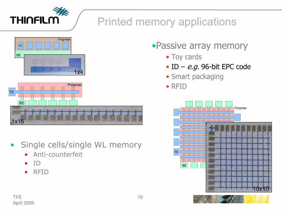
Printed memory applications
1x16
1x4
10x10
•Passive array memory• Toy cards• ID – e.g. 96-bit EPC code• Smart packaging• RFID
• Single cells/single WL memory• Anti-counterfeit• ID• RFID
TFEApril 2006
20
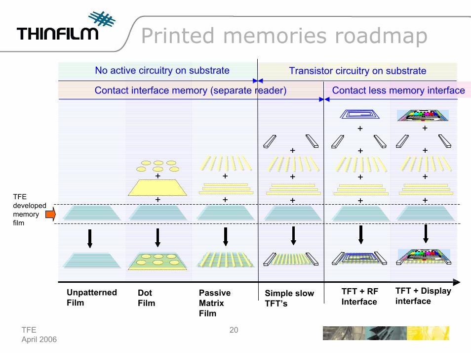
Printed memories roadmap
PassiveMatrixFilm
Simple slow TFT’s
+
+
+
+
+
+
+
+
+
+
+
+
+
+
+
TFE developed memory film
Contact less memory interface
No active circuitry on substrate Transistor circuitry on substrate
Contact interface memory (separate reader)
TFT + Display interface
TFT + RF Interface
UnpatternedFilm
Dot Film
TFEApril 2006
21
Shortage of memory technologies“The biggest opportunities for printed electronics include displays,
printed transistor circuits, RFID and sensor networks. Of course, these overlap. Some RFID tags include sensors and some have displays, many displays need transistor circuits to drive them. So this forms a tight pack of technologies all marching in step, with investment and invention nicely coordinated to tackle the fabulous market opportunities ahead? Not so. One thing is missing as we seek to print all of them and it is non volatile, preferably large memory. There may be hundred companies developing OLEDs and thirty developing thin film transistor circuits yet compatible printed memory - needed for almost everything we have mentioned - is being tackled only by a handful of organisations, most of them at the university - write a scientific paper -stage and with no chance of being ready on time. The result is that the first printed RFID tags will appear within the next two years with only a few bits of memory,making them virtually unsaleable.”
Source: IDTechEx Apr 18, 2005
TFEApril 2006
22
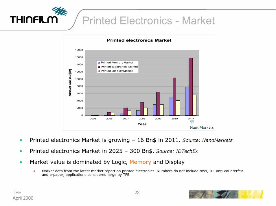
Printed Electronics - MarketPrinted electronics Market
0
2000
4000
6000
8000
10000
12000
14000
16000
18000
2005 2006 2007 2008 2009 2010 2011
Year
Mar
ket v
alue
($M
)
Printed Memory MarketPrinted Electronics MarketPrinted Display Market
NanoMarkets
• Printed electronics Market is growing – 16 Bn$ in 2011. Source: NanoMarkets
• Printed electronics Market in 2025 – 300 Bn$. Source: IDTechEx
• Market value is dominated by Logic, Memory and Display
• Market data from the latest market report on printed electronics. Numbers do not include toys, ID, anti-counterfeit and e-paper, applications considered large by TFE.
TFEApril 2006
23
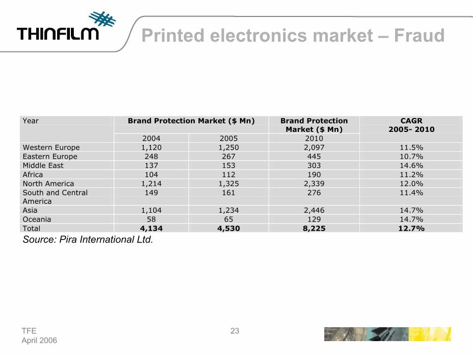
Printed electronics market – Fraud
Brand Protection Market ($ Mn) Brand Protection Market ($ Mn)
Year
2004 2005 2010
CAGR 2005- 2010
Western Europe 1,120 1,250 2,097 11.5% Eastern Europe 248 267 445 10.7% Middle East 137 153 303 14.6% Africa 104 112 190 11.2% North America 1,214 1,325 2,339 12.0% South and Central America
149 161 276 11.4%
Asia 1,104 1,234 2,446 14.7% Oceania 58 65 129 14.7% Total 4,134 4,530 8,225 12.7%
Source: Pira International Ltd.
TFEApril 2006
24
Board of Directors and new Managing Director
Proposed new Board of Directors
Jon Wiggen, (proposed Chairman). Mr. Wiggen is a state authorised public accountant, and has been a partner at Kjelstrup & Wiggen AS since 1993. He has strong experience on advising and auditing on valuations, as well as on mergers and acquisitions.
Ole J. Fredriksen, (proposed board member). Mr. Fredriksen holds a Bachelor of Science degree in Economics from the University of Bergen. He has 20 years experience in the computer hardware and software industry. Mr. Fredriksen was one of the co-founders of ASK (later Proxima, later InFocus). InFocus is listed on NASDAQ and previously on Oslo Børs, and is a global leading projector company in multimedia presentation and large display solutions. Mr. Fredriksen held the position as President & CEO of ASK (Proxima) for 15 years, and Chairman of Proxima Corp from 1998-2000. In 2000 Mr. Fredriksen became President of InFocus Corporation and Vice Chairman of the Board.
Hans Gude Gudesen, (proposed board member). Mr. Gudesen was co-founder of FAST and has served as a Non-Executive Director in FAST from July 1997 until 15 February 2006. He has previously (until 5 January 2006) served as a director of Opticom, a company he founded. Mr. Gudesen has coordinated a broad range of research and development projects in the fields of retrieval and data compression, which have resulted in the formation of a number of research and development companies, such as OPTICOM in Norway and Smart Materials S.A., a Belgian corporation.
Managing Director
Per Bröms. Mr. Bröms holds a Master of Science degree in Applied Physics and Electrical Engineering, and a PhD in Surface Physics and Chemistry from Linköping University. Mr. Bröms joined Thin Film Electronics in January 1999, and has extensive experience within Thin Films business areas and technology.
TFEApril 2006
25
Summary
• Thin Film Electronics memory technology is highly suitable for printed non volatile random access memory applications
• Fully printed small non volatile random access memories has been printed with ink-jet
• Applications requiring small memories (<1kbit) using external contact reader can be done today
• Future memory size and performance is limited by the printed transistor performance in a foreseeable future