Embed Size (px)
Citation preview

1
– Evaporation• Thermal evaporation• E-beam evaporation
– Sputtering• DC sputtering• RF sputtering• Reactive sputtering
– Chemical Vapor Deposition– Laser ablation– Spin-on/liquid deposition
• Spin-on glass and dopants• Sol-gel deposition
Thin film deposition
Vacuum requirement
• Long mean free path – Larger than 1m– pressure less than 5 x 10⁻⁶ Torr
• Free of reactive components– Oxygen
• Free of outgassing during evaporation

2
• Physical Vapor Deposition (PVD)– Film is formed by atoms directly
transported from source to the substrate.• Evaporation• Sputtering
• Chemical Vapor Deposition (CVD)– Film is formed by chemical reaction on
the surface of substrate.• SiO2, Si3N4, SiC, W CVD deposition• Atomic layer deposition• Crystal growth
• Evaporation– Thermal evaporation– E-beam evaporation
3
E-beam evaporationMaterial contained in a crucibleEvaporation of almost any material including refractory metalsNo control of volatile components/stoichiometric composition
Thermal E-beam
Temperature range
~ 1800°C ~ 3000°C
Deposition rate
0.1 ~ 2 nm/s 1 ~ 10 nm/s
Typical evaporant
Au, Ag, Al, Cr, Sn, Ga, Ti, NaCl, KCl, MgF2
AlsoPt, W, Ta, Zr, Al2O3, SiO2, TiO2, SnO2
4
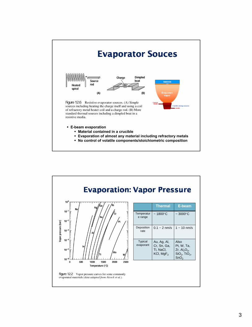
Shadowing effectsIncomplete step coverage
Mitigated by rotation & angled evaporation

5
3-Boat Evaporator• 3 separate evaporation
boats• Alloyed layers
– SnAu, AuGe
• Adhesion layers– Cr, Ti
• Protection layer– Au, Pt
Amorphous
Crystalline
6
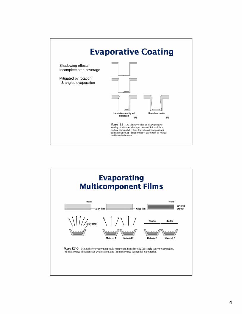
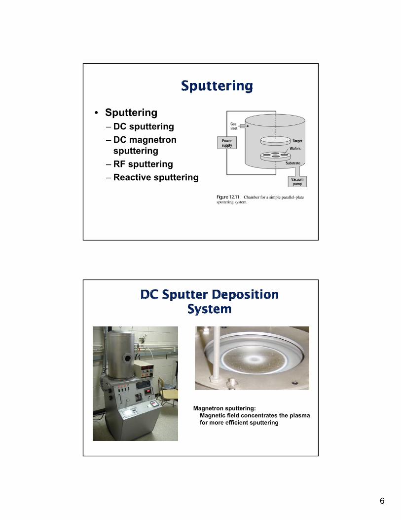
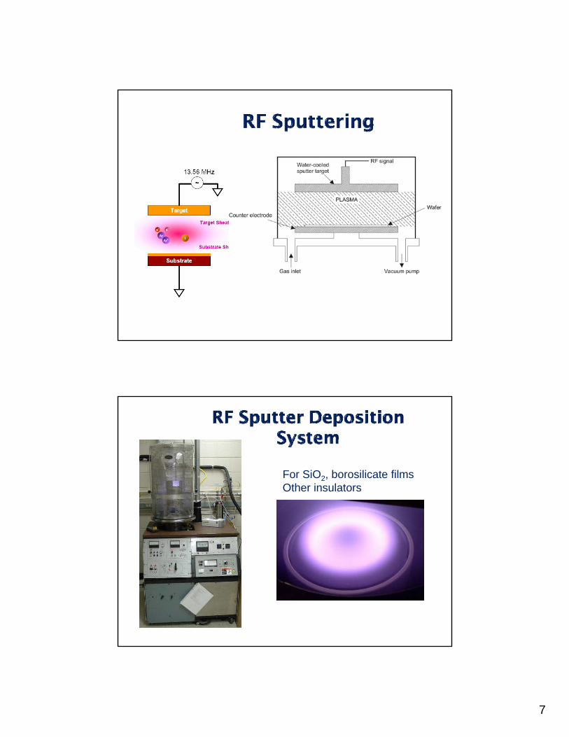
• Sputtering– DC sputtering– DC magnetron
sputtering– RF sputtering– Reactive sputtering
Magnetron sputtering:Magnetic field concentrates the plasma for more efficient sputtering
7
For SiO2, borosilicate filmsOther insulators
8
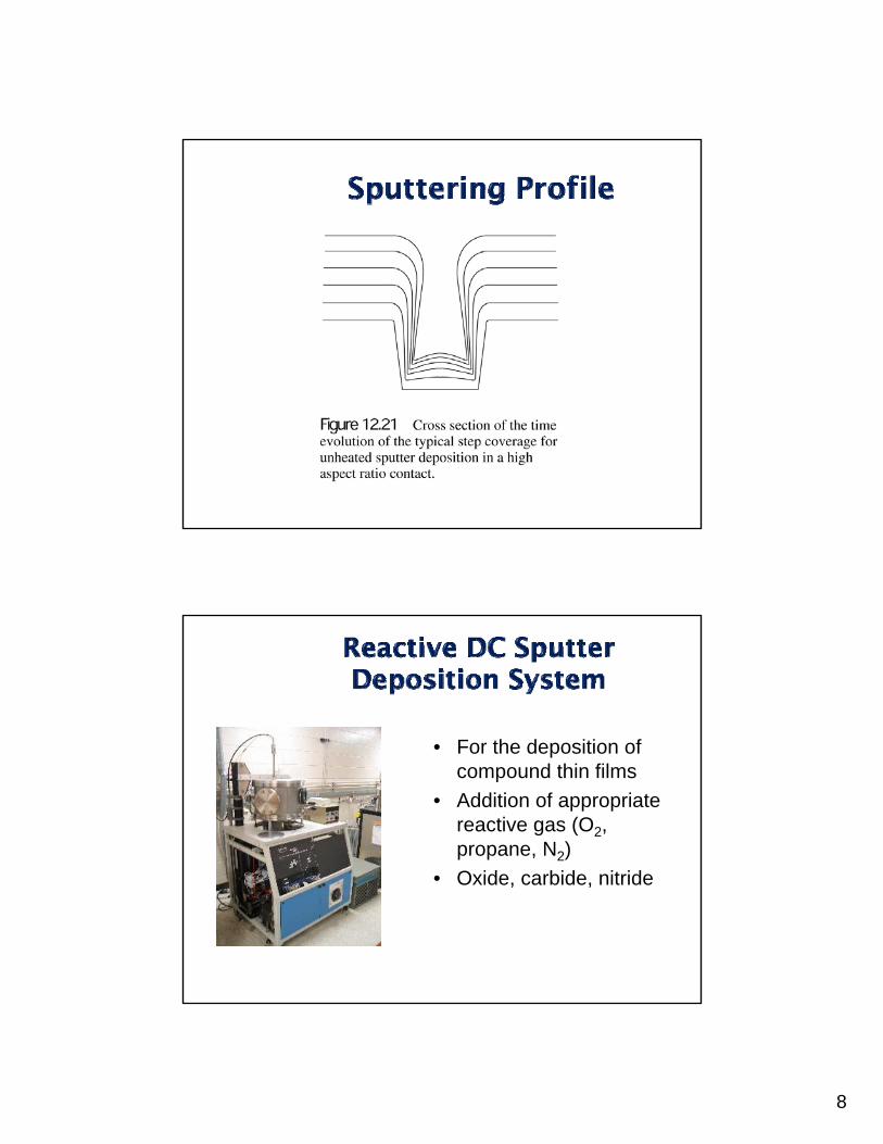
• For the deposition of compound thin films
• Addition of appropriate reactive gas (O2, propane, N2)
• Oxide, carbide, nitride
9
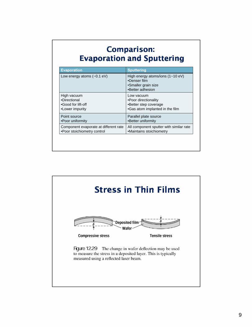
Evaporation SputteringLow energy atoms (~0.1 eV) High energy atoms/ions (1~10 eV)
•Denser film•Smaller grain size•Better adhesion
High vacuum•Directional•Good for lift-off•Lower impurity
Low vacuum•Poor directionality•Better step coverage•Gas atom implanted in the film
Point source•Poor uniformity
Parallel plate source•Better uniformity
Component evaporate at different rate•Poor stoichiometry control
All component sputter with similar rate•Maintains stoichiometry
10
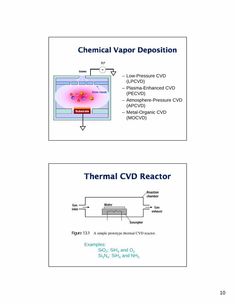
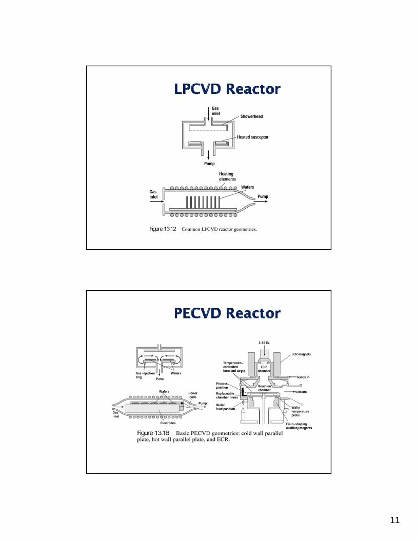
– Low-Pressure CVD (LPCVD)
– Plasma-Enhanced CVD (PECVD)
– Atmosphere-Pressure CVD (APCVD)
– Metal-Organic CVD (MOCVD)
Examples: SiO2: SiH4 and O2Si3N4: SiH4 and NH3
11
12
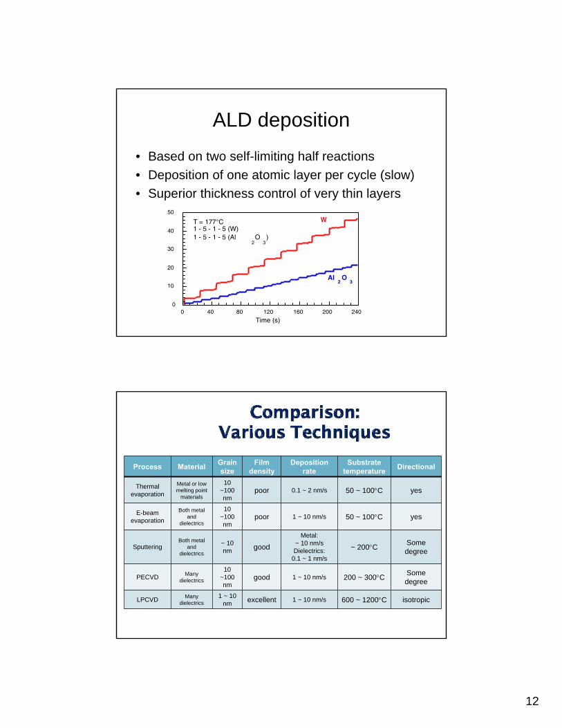
ALD deposition
• Based on two self-limiting half reactions• Deposition of one atomic layer per cycle (slow)• Superior thickness control of very thin layers
0
10 20 30 40 50
0 40 80 120 160 200 240
Time (s)
W
Al2
O3
T = 177°C 1 - 5 - 1 - 5 (W)1 - 5 - 1 - 5 (Al
2O
3)
Process Material Grain size
Film density
Deposition rate
Substrate temperature Directional
Thermal evaporation
Metal or low melting point
materials
10 ~100 nm
poor 0.1 ~ 2 nm/s 50 ~ 100°C yes
E-beam evaporation
Both metal and
dielectrics
10 ~100 nm
poor 1 ~ 10 nm/s 50 ~ 100°C yes
SputteringBoth metal
and dielectrics
~ 10 nm good
Metal: ~ 10 nm/sDielectrics:
0.1 ~ 1 nm/s
~ 200°C Some degree
PECVD Many dielectrics
10 ~100 nm
good 1 ~ 10 nm/s 200 ~ 300°C Some degree
LPCVD Many dielectrics
1 ~ 10 nm excellent 1 ~ 10 nm/s 600 ~ 1200°C isotropic
13
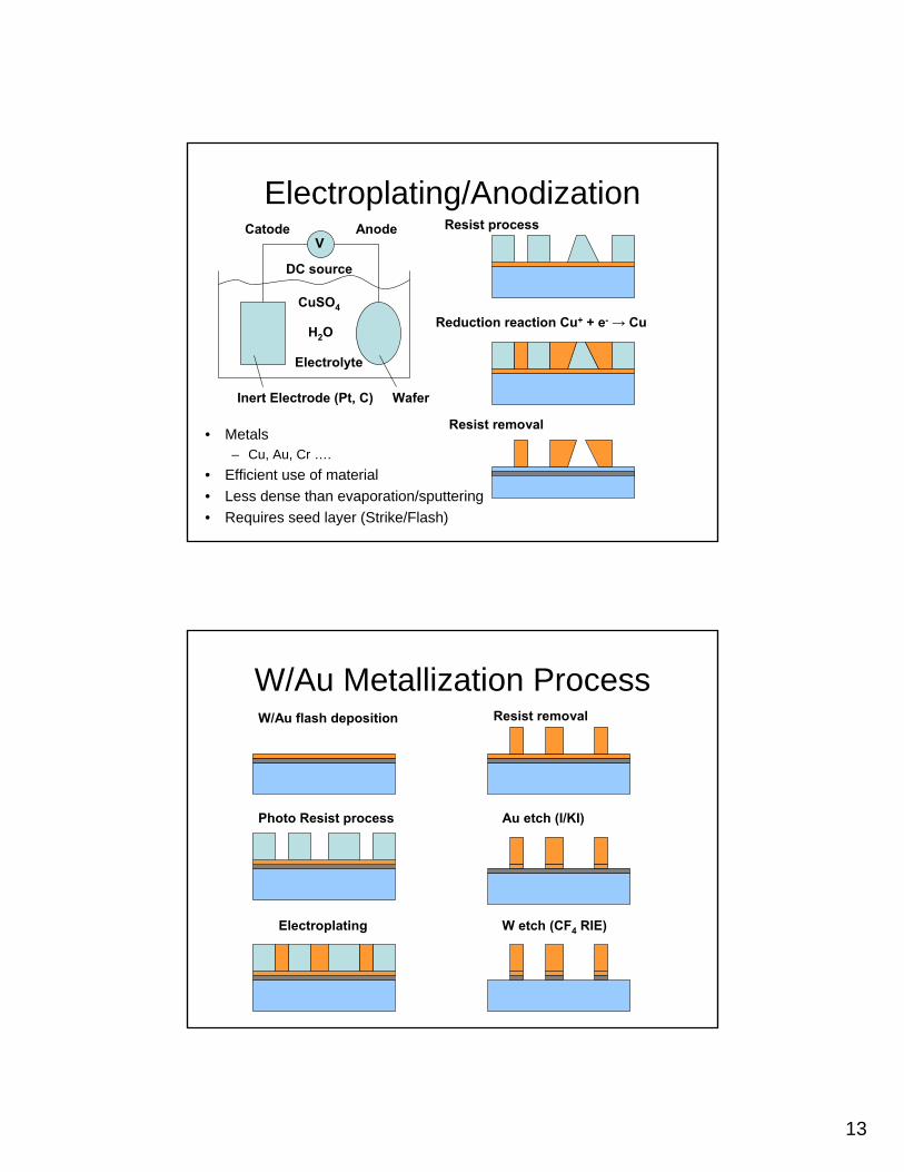
Electroplating/Anodization
Inert Electrode (Pt, C)
CuSO4
H2O
Electrolyte
Wafer
DC source
V
• Metals– Cu, Au, Cr ….
• Efficient use of material• Less dense than evaporation/sputtering• Requires seed layer (Strike/Flash)
Reduction reaction Cu+ + e- → Cu
AnodeCatode Resist process
Resist removal
W/Au Metallization ProcessW/Au flash deposition
Photo Resist process
Electroplating
Resist removal
Au etch (I/KI)
W etch (CF4 RIE)

14
– Laser ablation• Maintains composition• Used for perovskites
– Ferro-electric materials– High-temperature superconductors
– Spin-on/liquid deposition• Spin-on glass and dopants• Sol-gel deposition• Spray-on deposition
Alternate thin film deposition