Embed Size (px)
Citation preview
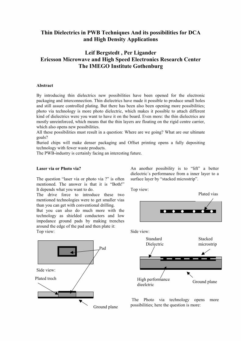
Thin Dielectrics in PWB Techniques And its possibilities for DCAand High Density Applications
Leif Bergstedt , Per LiganderEricsson Microwave and High Speed Electronics Research Center
The IMEGO Institute Gothenburg
Abstract
By introducing thin dielectrics new possibilities have been opened for the electronicpackaging and interconnection. Thin dielectrics have made it possible to produce small holesand still assure controlled plating. But there has been also been opening more possibilities;photo via technology is more photo dielectric, which makes it possible to attach differentkind of dielectrics were you want to have it on the board. Even more: the thin dielectrics aremostly unreinforced, which means that the thin layers are floating on the rigid centre carrier,which also opens new possibilities.All these possibilities must result in a question: Where are we going? What are our ultimategoals?Buried chips will make denser packaging and Offset printing opens a fully depositingtechnology with fewer waste products.The PWB-industry is certainly facing an interesting future.
Laser via or Photo via?
The question “laser via or photo via ?” is oftenmentioned. The answer is that it is “Both!”It depends what you want to do.The drive force to introduce these twomentioned technologies were to get smaller viasthan you can get with conventional drilling.But you can also do much more with thetechnology as shielded conductors and lowimpedance ground pads by making trenchesaround the edge of the pad and then plate it:Top view:
Side view:
An another possibility is to “lift” a betterdielectric´s performance from a inner layer to asurface layer by “stacked microstrip”.
Top view:
Side view:
The Photo via technology opens morepossibilities; here the question is more:
Pad
Plated trech
Ground plane
Ground plane
Stackedmicrostrip
StandardDielectric
High performancedieelctric
Plated vias
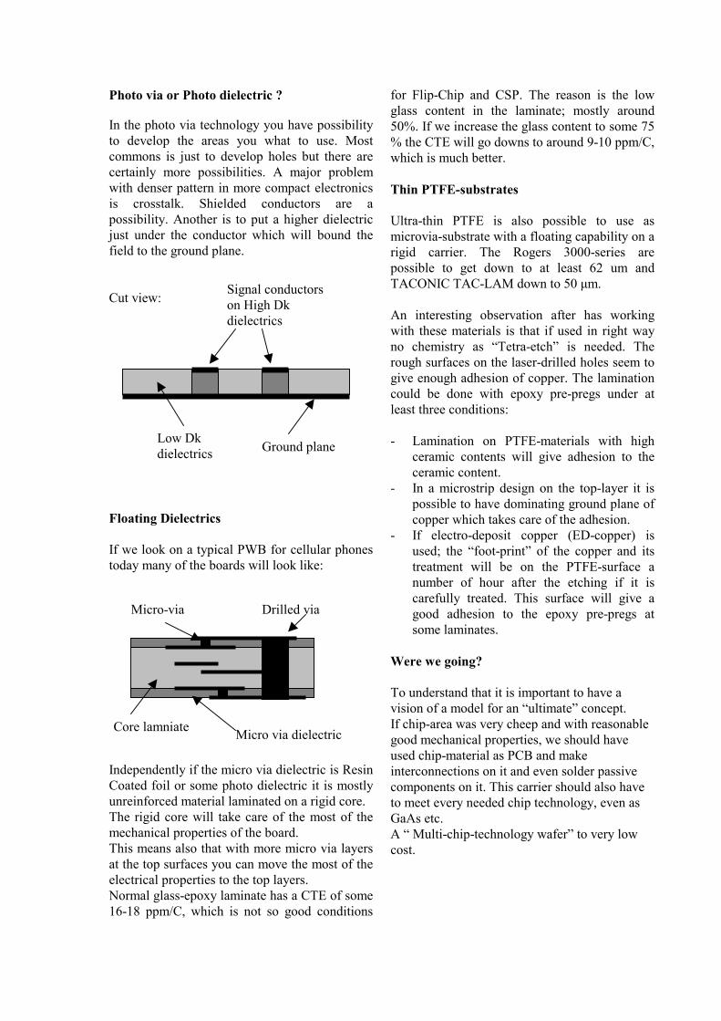
Photo via or Photo dielectric ?
In the photo via technology you have possibilityto develop the areas you what to use. Mostcommons is just to develop holes but there arecertainly more possibilities. A major problemwith denser pattern in more compact electronicsis crosstalk. Shielded conductors are apossibility. Another is to put a higher dielectricjust under the conductor which will bound thefield to the ground plane.
Cut view:
Floating Dielectrics
If we look on a typical PWB for cellular phonestoday many of the boards will look like:
Independently if the micro via dielectric is ResinCoated foil or some photo dielectric it is mostlyunreinforced material laminated on a rigid core.The rigid core will take care of the most of themechanical properties of the board.This means also that with more micro via layersat the top surfaces you can move the most of theelectrical properties to the top layers.Normal glass-epoxy laminate has a CTE of some16-18 ppm/C, which is not so good conditions
for Flip-Chip and CSP. The reason is the lowglass content in the laminate; mostly around50%. If we increase the glass content to some 75% the CTE will go downs to around 9-10 ppm/C,which is much better.
Thin PTFE-substrates
Ultra-thin PTFE is also possible to use asmicrovia-substrate with a floating capability on arigid carrier. The Rogers 3000-series arepossible to get down to at least 62 um andTACONIC TAC-LAM down to 50 μm.
An interesting observation after has workingwith these materials is that if used in right wayno chemistry as “Tetra-etch” is needed. Therough surfaces on the laser-drilled holes seem togive enough adhesion of copper. The laminationcould be done with epoxy pre-pregs under atleast three conditions:
- Lamination on PTFE-materials with highceramic contents will give adhesion to theceramic content.
- In a microstrip design on the top-layer it ispossible to have dominating ground plane ofcopper which takes care of the adhesion.
- If electro-deposit copper (ED-copper) isused; the “foot-print” of the copper and itstreatment will be on the PTFE-surface anumber of hour after the etching if it iscarefully treated. This surface will give agood adhesion to the epoxy pre-pregs atsome laminates.
Were we going?
To understand that it is important to have avision of a model for an “ultimate” concept. If chip-area was very cheep and with reasonablegood mechanical properties, we should haveused chip-material as PCB and makeinterconnections on it and even solder passivecomponents on it. This carrier should also haveto meet every needed chip technology, even asGaAs etc. A “ Multi-chip-technology wafer” to very lowcost.
Signal conductorson High Dkdielectrics
Low Dkdielectrics Ground plane
Micro-via Drilled via
Core lamniate Micro via dielectric

If this was possible we could forget all:- Problems with electrical connections
between chip and carrier, because they aremade on the same media.
- Problems with mechanical miss-matchbetween chip and carrier.
At the same time we have got a chip-thin carrierwith integrated chip. This is quite ultimate. Now chip-area is not very low-cost, and we needdifferent types of chip technology on the samecarrier, and after all chip-area is not so god aschip-carrier. But now we have a vision. Let’s try to get it. Chip-Thick Carrier As it is hard to have a total chip-area over thetotal carrier. Let’s implement a chip-thick chip-compatible carrier. This materiel should haveCTE corresponding to the actual used chip-technology, good mechanical properties andgood thermal conductivity. With this material it is possible to make holesfor the chip which are in close tolerances to theactual chip-sizes. Examples for this type ofmaterials are AlSi and AlSiC. Others arepossible as LTCC-based materials. The carrier could be copper-plated to get aproper ground-plane.
Chip-thick carrier from side:
From top:
The attachment of chips could either be done ona thin flexible metal-foil, which covers thebottom of the chip-cavities and the total bottom-side of the carrier. Or the chips could betemporary attached during this step and finallyattached during the operation “Buried bump”. Buried Bump The connection-areas on the chips; “bond-pads”can be prepared with “bumps” as final operationat the chip supplier before they are cut out fromthe wafer.
Chips with bumps with carrier; side view:
In our tests we have used “ball-bumps”, howeverplated bumps in the wafer-process is to prefer.By using bumped chips, which pass thedielectric, it is possible to meet the bumps withquite big connection-pads. The most oftendescribed method to connect the chip with laser-vias will give bigger problem to find and hit thesmall bondpads on the chip
Photo of ball-bumps of wire:
Active chipareas
Conductors Passivecomponents
Chips Carrier
”bumps”
Tail

Next step is to cover the carrier with liquiddielectric. Ball-bumps covered of lacquer:
After wet grinding (to much in this case) andplating:
This will give direct-connected conductorswithout soldering or conductive adhesions. Atleast one more SBU-layer with conductors couldbe applied. As the core carrier will have a chip-compatible CTE it is possible to attach a Flip-Chip anywhere on surface.
The possibilities with Offset printing.
The most ideal component carrier will have tomeet the same performance of patterndimensions as the chips they have tointerconnect. This to reduce the problems with“fan-out” from the chips.This will result of conductors down to some 5um or smaller.
Matching thickness of dielectrics for theseconductors will be some 5 - 15 um and via-connections between layers down to some 10 -30 um.
There is a need to bury or integrate more passiveelectrical components in the pattern of the PWB.This to lift out passive functions from the chips.
We have earlier mentioned the problems withcross-talk between different conductors and tohave different electrical performances atdifferent parts of the PWB.The present PWB technology has hard to meetthe demands mentioned above.Added to that the present PWB-technology is notan environmental friendly concept. We areetching away nearly more copper than is on thefinal board. A multilayerboard has a numberlessdevelopment and stripping operations of photo-resist and solder-resists.
Offset printing is a fully depositing method, allmaterial used will be on the final product. Theaccuracy is in the range we need.
Fig. A complete bible printed on one poster.Standard offset printing with distinct lettersmade of ”track-width” 25 um.
The limitation to introduce offset printing as apattern-transfer method has been the lowconductive inks based on silver or carbon.Reports of conductive polymers are coming butstill not commercial. During the time is possibleto use offset printed polymer activators as a preoperation for chemical copper.
Tail
”Bump”
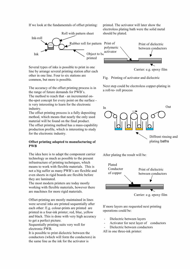
If we look at the fundamentals of offset printing:
Several types of inks is possible to print in oneline by arrange several printing station after eachother in one line. Four to six stations arecommon, but more is possible.
The accuracy of the offset printing process is inthe range of future demands for PWB’s.The method to reach that - an incremental on-the-spot concept for every point on the surface -is very interesting to learn for the electronicindustry.The offset printing process is a fully depositingmethod, which means that nearly the only usedmaterial will be found on the final product.The offset printing method has a mass-capabilityproduction profile, which is interesting to studyfor the electronic industry.
Offset printing adapted to manufacturing ofPWB
The idea here is to adapt the component carriertechnology as much as possible to the presentinfrastructure of printing techniques, whichmeans to work with flexible materials. This isnot a big suffer as many PWB’s are flexible andeven sheets in rigid boards are flexible beforethey are laminated.The most modern printers are today mostlyworking with flexible materials, however thereare machines for more rigid materials.
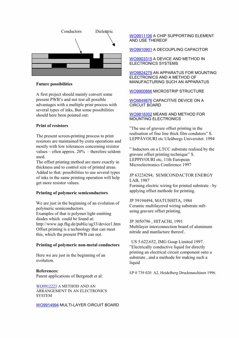
Offset-printing are mostly maintained in lineswere several inks are printed sequentially aftereach other: E.g. colour-prints are printed areprinted in a four-ink printer; red, blue, yellowand black. This is done with very high accuracyto get a perfect picture.Sequentially printing suits very well forelectronic PWB.It is possible to print dielectric between theconductors (which will form the conductors) inthe same line as the ink for the activator is
printed. The activator will later show theelectroless plating bath were the solid metalshould be plated.
Ink-roll
Ink
Roll with pattern sheet
Rubber roll for pattern
Object to bprinted
Print of dielectricbetween conductors
Print ofpolymericactivator
Fig. Printing of activator and dielectric
Next step could be electroless copper-plating ina roll-to- roll process
After plating the result will be:
If more layers are requested next printingoperations could be:
- Dielectric between layers- Activator for next layer of conductors- Dielectric between conductors
All in one three-ink printer:
e
Carrier: e.g. epoxy film
Diffrent rinsing andplating baths
In Out
Print of dielectricbetween conductors
Carrier: e.g. epoxy film
PlatedConductorof copper
Future possibilities
A first project should mainly convert somepresent PWB’s and not test all possibleadvantages with a multiple print process withseveral types of inks, But some possibilitiesshould here been pointed out:
Print of resistors
The present screen-printing process to printresistors are maintained by extra operations andmostly with low tolerances concerning resistorvalues – often approx. 20% – therefore seldomused.The offset printing method are more exactly inthickness and to control size of printed areas.Added to that: possibilities to use several typesof inks in the same printing operation will helpget more resistor values.
Printing of polymeric semiconductors
We are just in the beginning of an evolution ofpolymeric semiconductors.Examples of that is polymer light emittingdiodes which could be found at:http://www.iap.fhg.de/public/ag33/device1.htmOffset printing is a technology that can meetthis, which the present PWB can not.
Printing of polymeric non-metal conductors
Here we are just in the beginning of anevolution.
References:Patent applications of Bergstedt et al:
WO9912223 A METHOD AND ANARRANGEMENT IN AN ELECTRONICSSYSTEM
WO9914994 MULTI-LAYER CIRCUIT BOARD
WO9911106 A CHIP SUPPORTING ELEMENTAND USE THEREOF
WO9910901 A DECOUPLING CAPACITOR
WO9903315 A DEVICE AND METHOD INELECTRONICS SYSTEMS
WO9824279 AN APPARATUS FOR MOUNTINGELECTRONICS AND A METHOD OFMANUFACTURING SUCH AN APPARATUS
WO9900866 MICROSTRIP STRUCTURE
WO9849876 CAPACITIVE DEVICE ON ACIRCUIT BOARD
WO9818302 MEANS AND METHOD FORMOUNTING ELECTRONICS
”The use of gravure offset printing in therealisation of fine line thick film condutors” S.LEPPÅVOURI etc Uleåborgs Universitet. 1994
” Inductors on a LTCC substrate realised by thegravure offset printing technique” S.LEPPIVOURI etc, 11th EuropeanMicroelectronics Conference 1997
JP 63224294, SEMICONDACTOR ENERGYLAB, 1987Forming electric wiring for printed substrate - byapplying offset methode for printing.
JP 59194494, MATUSHITA, 1984Ceramic multilayered wiring substrate mfr-using gravure offset printing.
JP 3050796 , HITACHI, 1991Multilayer interconnection board of aluminumnitride and manfacture thereof..
US 5.622.652, IMG Goup Limited 1997.”Electrically conductive liquid for directlyprinting an electrical circuit component onto asubstrate , and a methode for making such aliquid
EP 0 739 020 A2, Heidelberg Druckmaschinen 1996.
DielectricConductors


![PWB Handbook[1]](https://img.pdfslide.us/doc/110x75/577d25b71a28ab4e1e9f734a/pwb-handbook1.jpg)