Embed Size (px)
Citation preview
Thin autofocus camera module by a large-stroke micromachined deformable mirror
Hsin-Ta Hsieh,1 Hsiang-Chun Wei,
1 Meng-Hsuan Lin,
1 Wei-Yao Hsu,
2
Yuan-Chieh Cheng,2 and Guo-Dung John Su,
1,*
1Graduate Institute of Photonics and Optoelectronics, National Taiwan University, No. 1, Sec. 4, Roosevelt Road, Taipei, 10617 Taiwan
2Instrument Technology Research Center, National Applied Research Laboratories, 20, R&D Rd. VI, Hsinchu Science Park, Hsinchu 300, Taiwan
Abstract: The conventional auto-focus and zoom image systems were made by a set of motor-moved lenses. Because of mechanical moving parts, it is not easy to miniaturize their sizes. In this paper, we propose a thin autofocus system using a large stroke MEMS (micro-electro-mechanical systems) deformable mirror which has the potential to downscale the size and to minimize chromatic aberration. The large stroke MEMS deformable mirror is made by a polyimide membrane that has a maximum 12 µm displacement over a 3 mm aperture. The module size is 5.4 mm thick in optical design layout and 6.7 mm after packaging. This autofocus system is designed with the f-number = 4.13, on-axis MTF = 0.28 at full frequency of 230 cycles/mm, and incident light within ± 26 degree. The position of clear image can vary from 4 cm to 50 cm achieved by controlling the surface curvature of the MEMS deformable mirror.
©2010 Optical Society of America
OCIS codes: (220.0220) Optical design and fabrication; (220.4610) Optical fabrication.
References and links
1. R. C. Gutierrez, T. K. Tang, R. Calvet, and E. R. Fossum, “MEMS digital camera,” Proc. SPIE 6502, paper36, 1–8 (2007).
2. S. Kuiper, and B. H. W. Hendriks, “Variable-focus liquid lens for miniature cameras,” Appl. Phys. Lett. 85(7), 1128–1130 (2004).
3. H. Ren, Y. Fan, S. Gauza, and S. Wu, “Tunable-Focus Cylindrical Liquid Crystal Lens,” Jpn. J. Appl. Phys. 43(2), 652–653 (2004).
4. J. L. Wang, T. Y. Chen, Y. H. Chien, and G. D. Su, “Miniature optical autofocus camera by micromachined fluoropolymer deformable mirror,” Opt. Express 17(8), 6268–6274 (2009).
5. D. Wick, “Active Optical Zoom System,” US patent 6,977,777 (2005). 6. W. Smith, Modern Optical Engineering: the design of optical systems, 2nd, (McGraw-Hill, 1990), pp.436. 7. E. Hecht, Optics, 4nd (Addison Wesley, 2001). 8. Boston Micromachines Corporation, http://www.bostonmicromachines.com/. 9. V. T. Srikar, and S. M. Spearing, “Materials selection for microfabricated electrostatic actuators,” Sens.
Actuators A Phys. 102(3), 279–285 (2003). 10. K. Seidl, J. Knobbe, and H. Grüger, “Design of an all-reflective unobscured optical-power zoom objective,”
Appl. Opt. 48(21), 4097–4107 (2009). 11. J. Wang, T. Chen, C. Liu, C. Chiu, and G. Su, “Polymer Deformable Mirror for Optical Auto Focusing,” ETRI
Journal 29(6), 817–819 (2007).
1. Introduction
Conventional autofocus or zoom systems require a set of lenses and need large space because of mechanical motors. Recently, a MEMS-based motion control stage is used to minimize the space of mechanical motors [1]. However, manipulation of the space between lenses is not the only way to change the effective optical power. It also could be done by either varying the surface curvature or changing the refractive index distribution. These methods can be generally divided into refractive type and reflective type. Liquid lens [2] and liquid crystal lens (LC lens) [3] belong to refractive type. Liquid lens adopts bi-liquid lenses that can deform the shape of the interface between two immiscible liquids by electro-wetting method.
#126512 - $15.00 USD Received 5 Apr 2010; revised 4 May 2010; accepted 4 May 2010; published 11 May 2010(C) 2010 OSA 24 May 2010 / Vol. 18, No. 11 / OPTICS EXPRESS 11097

Liquid crystals (LCs) are excellent electro-optic materials with electrical and optical anisotropies. The optical properties can be controlled easily by external electric field. According to the change of refractive indices, the light can be converged and diverged. However, both liquid lens and liquid crystal lens need to utilize refractive design forms that require straight optical path. This fundamentally limits packaging thickness.
Another solution is reflective type, which adopts MEMS deformable mirrors (MEMS DM) to vary the optical power by deforming reflecting surfaces [4,5]. The advantage of reflective type is chromatic aberration free [6]. Besides, the straight optical path can be folded to reduce packaging thickness. DMs could be embedded with wave front sensors to correct the wavefront aberration for astronomical observation [7]. The system is commercialized for years [8]. Traditionally, MEMS DMs are made by inorganic materials, such as silicon or silicon nitride. These materials have high mechanical stiffness, which limits their deformation range [9]. The deformation of MEMS DM presented in this paper is about one order of magnitude higher than commercial products. In this paper we propose an optical system using a polymer MEMS DM in a reflective design form. The polymer MEMS DM could achieve 12-µm displacement over a 3-mm aperture that corresponds to about 20 diopter focusing power. The optical layout design is 5.4 mm thick and 6.7 mm after packaging. The optical system design, performance analysis, experimental results are discussed in following sections.
2. Optical System Design with Autofocus Function
The autofocus module in this paper was designed in a Z-shape configuration, which consists of two solid lenses, a free-form shape mirror, a polymer MEMS DM, an aperture stop, and a 1/4” 2M pixels (2.2 µm × 2.2 µm per pixel) image sensor. The lens 1 is a diverging lens with negative power and the lens 2 is a converging lens with positive power. The function of lens 1 and lens 2 is to focus objects on to an image plane. There is a free-form shape mirror at the last surface to eliminate the residual on-axis aberrations because of large incident angle on lens surfaces. The total effective focal length is about 5.7 mm, f-number is 4.13, and the incident light is within ± 26 degree as show in Fig. 1(a). However, the vignetting exists for light at large field angle and the off-axis aberrations degrade the MTF. The system can be optimized by carefully optimize other solid lenses and reflecting surfaces as in [10]. The total thickness is about 5.4 mm due to folded light beams. The best performance is on-axis, and the MTF drops to 30 cycles/mm at 26-degree field angle. Figure 1(b) shows the on-axis MTF of the system when the object is placed at 500 mm and the MEMS deformable mirror is flat. At this distance, the object is considered far compared with the effective focal length of the system. The modulation is above 20% at the full frequency of 230 cycles/mm. The full frequency is determined by the size of the imaging pixel, which is 2.2 µm in this case. One can see that the total optical path is about 18 mm, but the thickness can be reduced to about 5 mm by folding its optical path. This means that we could adopt longer optical path designs to release high power lenses requirement. In other words, we could use solid lenses with lower power that are easier to be fabricated and cause less aberration. This reflective design also gives us flexibility of accommodating larger image sensors without increasing packaging thickness too much.
#126512 - $15.00 USD Received 5 Apr 2010; revised 4 May 2010; accepted 4 May 2010; published 11 May 2010(C) 2010 OSA 24 May 2010 / Vol. 18, No. 11 / OPTICS EXPRESS 11098

Deformable
Mirror
FreeForm
Mirror
Lens 1
Lens 2Stop
Image
Sensor
(a) (b)
Fig. 1. (a) Optical system design in reflective form, and (b) its modulation transfer function (MTF) when a MEMS deformable mirror is flat for far objects
When an object is placed closer to the autofocus module, the image position is expected to move away from the original position. To amend the image position change, the focusing power of a MEMS deformable mirror must be changed accordingly. When the object position is changed from 500 to 44 mm, the focusing power of a MEMS DM must be adjusted from 0 to 20 m−1 (i.e. flat to curve) in the optical system of Fig. 1(a). The image of lady Lenna was simulated by ZEMAX® to illustrate this change. Figure 2(a) shows the image analysis simulation calculated by ray tracing method. We can observe that it will focus on 500 mm object with a flat MEMS DM. If the object is brought to 44 mm from the lens 1, we need to actuate MEMS DM to 20 diopter focusing power, which is approximately corresponding to 100 mm radius of curvature. Figure 2(b) shows the MTF of the optical system when the deformable is actuated to 20-diopter and the object is placed at 44 mm. One can see the MTF dropped slightly compared to a flat mirror, but still above 20% at the full frequency.
Object = 44 mm Object = 500 mm
Ac
tua
ted
F
lat
(a) (b)
Fig. 2. (a) Image simulation results of Lady Lenna, and (b) its modulation transfer function (MTF) when a MEMS deformable mirror is actuated for near objects.
3. Device Fabrication and Experimental Results
The key component of the autofocus module is MEMS DM. The MEMS DM in this paper consists of two parts. One is a deformable membrane and the other is a bottom electrode. A deformable membrane is a mirror made of a thin polyimide layer coated with aluminum reflecting layers and is actuated by electrostatic force. The deformable mirror was fabricated by MEMS technology. In deformable mirror part, we started from a (100) silicon wafer that is double side polished. A 6000 Å thermal oxide was grown for masking layer in wet etching process. Then, we patterned a square opening window on one side of oxide. We etched the non-PR covered region of oxide by BHF and remove PR after etching finished, as shown in Fig. 3(b). The wafer was dipped into a 90 °C TMAH solution for about 8 hours wet etching
#126512 - $15.00 USD Received 5 Apr 2010; revised 4 May 2010; accepted 4 May 2010; published 11 May 2010(C) 2010 OSA 24 May 2010 / Vol. 18, No. 11 / OPTICS EXPRESS 11099

tank and this resulted in a 25-µm residual silicon layer as Fig. 3(c). The Al/Cr (1200 Å / 200 Å) layer were evaporate on the flatten side. Aluminum layer will become reflection layer and chromium layer can solve the adhesion problem. The polyimide PI-2610 from Dupont® was spun at 4000 rpm for 60 seconds and was cured at 300 °C for 30 minutes in furnace to form a polymer layer on aluminum. We evaporated another Al (1200 Å) layer for electrode and this formed a sandwich structure with polymer and previous Al layer as Fig. 3(e). We choose the polyimide because similar coefficient of thermal expansion to Si substrate results in low thermal strain and low residual stress. The sandwich configuration balances the residual stress on double side of polymer layer. A PR (photoresist) layer was spun and an elliptical opening was defined on it to form an elliptical outside frame of a DM as Fig. 3(f). The opening of the photoresist can be changed accordingly to fit into optical system design. In our design, the silicon opening is a 3.5 mm square and the PR opening is a 3 mm ellipse. The thickness of the PR opening is 20 µm and is used to define the deflection shape of the polyimide membrane. Finally, we removed the residual Si layer by XeF2 and etched the oxide and Cr layer on reflection Al layer as shown in Fig. 3(f). The remaining oxide on the membrane was then removed by Pad Etchant S (from AUECC, Taiwan.), which minimizes damage to metal layers unlike traditional buffered hydrogen fluoride (HF).
Regarding the bottom electrode part, a conducting Al/Cr layer was evaporated on a flatten wafer with an isolation oxide layer. In Fig. 3(g), PR pillars were patterned to form air channels and short-circuit protection stoppers, which prevent DM from damage at snap down voltage. These air channels are important to improve the response time of the membrane because a sealed cavity underneath the membrane will slow down the moving speed of a membrane due to air damping effect. The thickness of the pillar is 12 µm so that the total gap between the polyimide membrane and the bottom Al electrode is 32 µm. This provides enough spacing for the membrane to deform to 20-diopter before snapping down caused by electrostatic force. Finally, top membrane and bottom electrode were bonded together by 100N force at 120C for 60 minutes. In order to connect the wires from the back side of DM, two small cavities were opened in TMAH etching step. Two conducting wires were attached on a DM by conductive epoxy. Due to the tensile residual stress of the polyimide membrane, the reflecting surface is very flat [4].
(c) TMAH etching
(d) 1st metal layer evaporation
(f) PR frame & Release Si and SiO2
(100)
(a) Thermal oxidation
(b) Oxide etching
Si wafer
(h) Al evaporation
(100)
(g) Thermal oxidation
Si wafer
(i) PR pillar
(e) Polymer layer & 2nd metal layer
PR
V
SiO2
MetalPolymerPR
Top membraneBottom membrane
Fig. 3. Device fabrication processes for a top polymer membrane and a bottom electrode.
A cross-section schematic drawing in Fig. 4(a) shows a flat membrane surface without applied voltage. One can see the polyimide membrane is supported by a silicon frame. The PR
#126512 - $15.00 USD Received 5 Apr 2010; revised 4 May 2010; accepted 4 May 2010; published 11 May 2010(C) 2010 OSA 24 May 2010 / Vol. 18, No. 11 / OPTICS EXPRESS 11100

defines the circular opening of the reflecting mirror surface. When a voltage is applied between the deformable membrane and the bottom electrode, the membrane is pulled down by electrostatic force and forms a curved surface to focus light, as in Fig. 4(b). The PR pillars allow the air to flow out the gap without damping the motion of the polyimide membrane. Besides, they also prevent short circuit damages when the membrane is in touch with the bottom Al electrode. We also purposely sandwiched the polyimide layer with two aluminum layers so that the residual stress of metal layers are balanced out by this symmetric configuration. In addition, the polyimide is all covered with metal layers, preventing it from in contact with oxygen and moisture in air. We found this increases the membrane reliability compared with only one side aluminum coating. A fabricated device is shown in Fig. 0.4(c) where the bottom electrode is underneath the membrane and cannot be seen from this angle of view. The diced chip is 6.5 mm in width with a 3.5 mm square opening. The lower part of the diced chip is designed to be mounted on a package base later. The optical aperture of this MEMS DM is 3 mm because the photoresist define its deflection area as illustrated in Fig. 3(f).
Fig. 4. Schematic drawings and photos of a fabricated MEMS deformable mirror device
We measured the center displacement versus applied voltage of the polymer MEMS DM. A DC-DC voltage amplifier circuit (From Matsusada Precision Inc.) is used to increase the input voltage from 15V to maximum 600V output. Although the applied voltage is high, the power consuming is very low due to capacitor structure with negligible current (~nA statically). The optical power of the polymer DM is about reciprocal of half of the radius of curvature of the mirror surface. The diopter is calculated according to the first-order paraxial rays approximation [11], the radius of the curvature is calculated by the expression
2
16,
xP
D= (1)
where P is the focusing power in unit of diopter (m−1), D is diameter of the polymer membrane, and x is the deformation of the mirror from the center to the edge. The clear aperture is 3 mm in diameter and maximum center displacement is around 12 µm so the diopter is approximately 20 m−1 at 150V applied voltage. The experimental results are shown in Fig. 5.
#126512 - $15.00 USD Received 5 Apr 2010; revised 4 May 2010; accepted 4 May 2010; published 11 May 2010(C) 2010 OSA 24 May 2010 / Vol. 18, No. 11 / OPTICS EXPRESS 11101
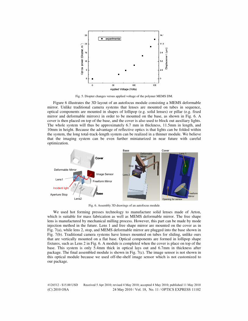
Fig. 5. Diopter changes versus applied voltage of the polymer MEMS DM.
Figure 6 illustrates the 3D layout of an autofocus module consisting a MEMS deformable mirror. Unlike traditional camera systems that lenses are mounted on tubes in sequence, optical components are mounted in shapes of lollipop (e.g. solid lenses) or pillar (e.g. fixed mirror and deformable mirrors) in order to be mounted on the base, as shown in Fig. 6. A cover is then placed on top of the base, and the cover is also used to block out auxiliary lights. The whole system will thus be approximately 6.7 mm in thickness, 11.5mm in length, and 10mm in height. Because the advantage of reflective optics is that lights can be folded within the system, the long total-track-length system can be realized in a thinner module. We believe that the imaging system can be even further miniaturized in near future with careful optimization.
Image SensorDeformable Mirror
BaseBaseBaseBase
CoverCoverCoverCover
Lens1
Lens2Aperture Stop
Freeform Mirror
Incident light
Lens 1
Lens 2
Stop
Deformable Mirror
Freeform Mirror
BaseBaseBaseBase CoverCoverCoverCover
Opening for sensor
Fig. 6. Assembly 3D drawings of an autofocus module
We used hot forming presses technology to manufacture solid lenses made of Arton, which is suitable for mass fabrication as well as MEMS deformable mirror. The free shape lens is manufactured by mechanical milling process. However, this part can be made by mode injection method in the future. Lens 1 and free shape mirror are mounted on the cover as in Fig. 7(a), while lens 2, stop, and MEMS deformable mirror are plugged into the base shown in Fig. 7(b). Traditional camera systems have lenses mounted on tubes for sliding, unlike ours that are vertically mounted on a flat base. Optical components are formed in lollipop shape fixtures, such as Lens 2 in Fig. 6. A module is completed when the cover is place on top of the base. This system is only 5.4mm thick in optical lays out and 6.7mm in thickness after package. The final assembled module is shown in Fig. 7(c). The image sensor is not shown in this optical module because we used off-the-shelf image sensor which is not customized to our package.
#126512 - $15.00 USD Received 5 Apr 2010; revised 4 May 2010; accepted 4 May 2010; published 11 May 2010(C) 2010 OSA 24 May 2010 / Vol. 18, No. 11 / OPTICS EXPRESS 11102

Freeform
mirror
Lens 1
Cover
Deformable
Mirror
Stop Lens 2
Base Autofocus
Module
(a) (b) (c)
Fig. 7. (a) Cover with a freeform mirror, (b) base with polymer MEMS DM and (c)final Assembly module
Figure 8 shows the experimental results of optical auto-focusing function in this module. The incident light is within ± 26 degree, and focus is on a 6-mm-diameter-circle in the image plane. However, the size of 2M pixel sensors is 3.52 mm x 2.64 mm, which is covered within a 4.4-mm-diameter-circular. In other words, the edge of image circular is chopped due to the size of sensor. When object was placed in the far distance, the clear image happened without actuating the MEMS DM. The far object (~160 mm in distance, 80 mm in height) shows few Chinese characters and English words written as “made from natura”.On the other hand, when object was at the near distance (~78 mm in distance, 40 mm in height), the clear image happened when the polymer MEMS DM was actuated. Numbers, 6 and 3 can be seen clearly. In principle, the autofocus function is achieved in this module. The images, however, were not as sharp as we originally predicted. This may be due to no anti-reflection coating on the lenses surfaces, misalignment of each component and/or partially imperfect solid lenses. We believe that all of these can be improved for a commercial product. Nevertheless, the concept of using MEMS deformable mirrors in a folded optical design can be realized in a thin package and demonstrated in the work. A video of autofocusing is also provided with this paper.
Fig. 8. Pictures of near and far objects (Media 1).
4. Conclusion
In this paper, we have presented a innovative auto-focusing system featuring a reflective design form and an organic polymer membrane deformable mirror. As the simulation results shown above, it can peform the optical autofocus function without stepping motors and moving lenses. The over size of the packaged module is 6.7 mm in thickness, 11.5 mm in length, and 10 mm in height. The power consumption is low becuase the polymer MEMS DM is actuated by elecctrotstatic force. We will also work on system improvement and add zooming function in the future. The MEMS deformable mirror indeed has focus-varying
#126512 - $15.00 USD Received 5 Apr 2010; revised 4 May 2010; accepted 4 May 2010; published 11 May 2010(C) 2010 OSA 24 May 2010 / Vol. 18, No. 11 / OPTICS EXPRESS 11103

function, and the optical image system we designed also provide the ability to focus on object in different distances. This paper demonstrates that a MEMS deformable mirror and folded optical system design can form a thin optical module for imaging applications and mobile electronic devices.
Acknowledgments
The authors would gratefully like to acknowledge National Science Council of Taiwan for their funding support under NSC 98-2622-E-002-012-CC3.
#126512 - $15.00 USD Received 5 Apr 2010; revised 4 May 2010; accepted 4 May 2010; published 11 May 2010(C) 2010 OSA 24 May 2010 / Vol. 18, No. 11 / OPTICS EXPRESS 11104