Embed Size (px)
Citation preview
General Features
Applications
Part Numbering
General
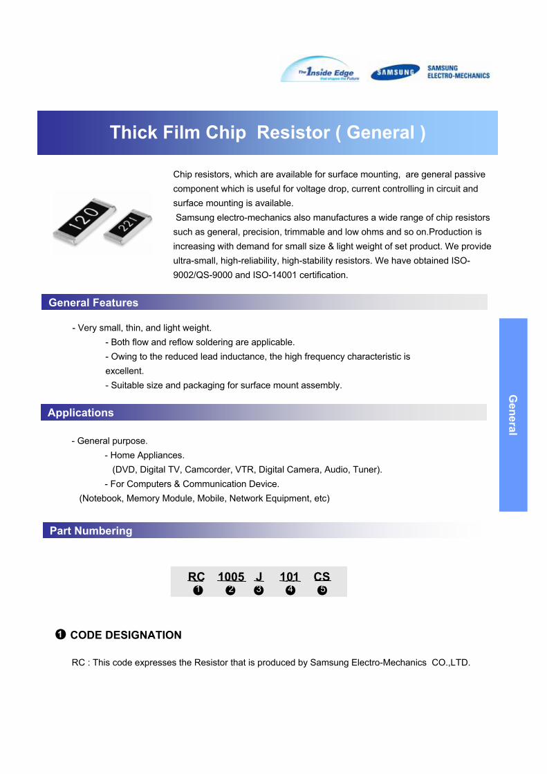
RC 1005 J 101 CS1 2 3 4 5
Thick Film Chip Resistor ( General )
CODE DESIGNATION1
RC : This code expresses the Resistor that is produced by Samsung Electro-Mechanics CO.,LTD.
Chip resistors, which are available for surface mounting, are general passive component which is useful for voltage drop, current controlling in circuit and surface mounting is available.Samsung electro-mechanics also manufactures a wide range of chip resistors such as general, precision, trimmable and low ohms and so on.Production is increasing with demand for small size & light weight of set product. We provide ultra-small, high-reliability, high-stability resistors. We have obtained ISO-9002/QS-9000 and ISO-14001 certification.
- Very small, thin, and light weight.- Both flow and reflow soldering are applicable.- Owing to the reduced lead inductance, the high frequency characteristic is excellent.- Suitable size and packaging for surface mount assembly.
- General purpose.- Home Appliances.
(DVD, Digital TV, Camcorder, VTR, Digital Camera, Audio, Tuner).- For Computers & Communication Device.
(Notebook, Memory Module, Mobile, Network Equipment, etc)
General
RESISTANCE TOLERANCE3
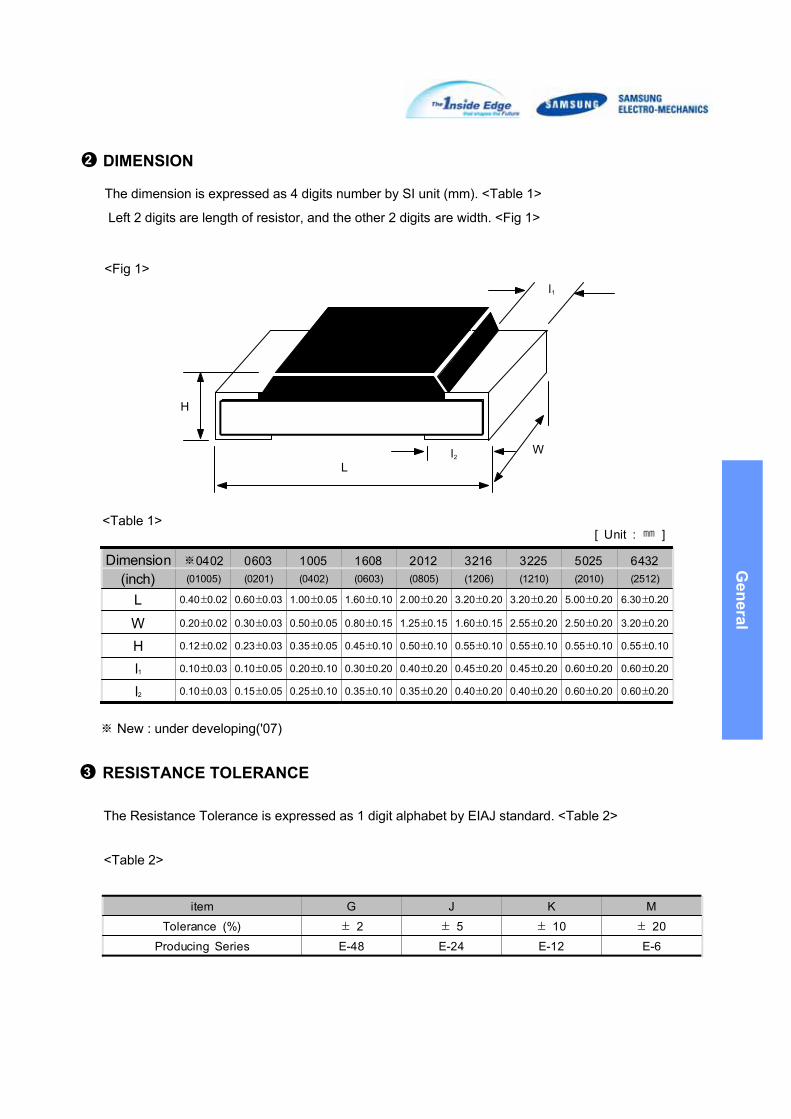
<Fig 1>
The Resistance Tolerance is expressed as 1 digit alphabet by EIAJ standard. <Table 2>
<Table 2>
The dimension is expressed as 4 digits number by SI unit (mm). <Table 1>
Left 2 digits are length of resistor, and the other 2 digits are width. <Fig 1>
Ll2
l1
W
H
item G J K M
Tolerance (%) ± 2 ± 5 ± 10 ± 20
Producing Series E-48 E-24 E-12 E-6
Dimension ※0402 0603 1005 1608 2012 3216 3225 5025 6432(inch) (01005) (0201) (0402) (0603) (0805) (1206) (1210) (2010) (2512)
L 0.40±0.02 0.60±0.03 1.00±0.05 1.60±0.10 2.00±0.20 3.20±0.20 3.20±0.20 5.00±0.20 6.30±0.20
W 0.20±0.02 0.30±0.03 0.50±0.05 0.80±0.15 1.25±0.15 1.60±0.15 2.55±0.20 2.50±0.20 3.20±0.20
H 0.12±0.02 0.23±0.03 0.35±0.05 0.45±0.10 0.50±0.10 0.55±0.10 0.55±0.10 0.55±0.10 0.55±0.10
l1 0.10±0.03 0.10±0.05 0.20±0.10 0.30±0.20 0.40±0.20 0.45±0.20 0.45±0.20 0.60±0.20 0.60±0.20
l2 0.10±0.03 0.15±0.05 0.25±0.10 0.35±0.10 0.35±0.20 0.40±0.20 0.40±0.20 0.60±0.20 0.60±0.20
[ Unit : ]<Table 1>
※ New : under developing('07)
DIMENSION2
General
The Nominal Resistance Value is expressed as 3 or 4 digits based on EIAJ standard. <Table 3>
<Table 3>
The Packaging Code is expressed as 2 digits alphabet. <Table 4>
<Table 4>
PackagingCode Description Dimension Packaging Q'ty
C S 7" REEL PACKAGING
0603 15,000 PCS
1005 10,000 PCS
1608, 2012, 3216, 3225 5,000 PCS
5025, 6432 4,000 PCS
E S 10" REEL PACKAGING 1608, 2012, 3216 10,000 PCS
A S 13" REEL PACKAGING
1005 40,000 PCS
1608, 2012, 3216, 3225 20,000 PCS
5025, 6432 15,000 PCS
G S BULK CASE PACKAGING
1608 25,000 PCS
2012 10,000 PCS
3216 5,000 PCS
item 3 digits mark(E-24) 4 digits mark(E-48)
Resistance
ToleranceG, J, K, M G
Only numberFirst 2 digits : Resistance valueLast 1 digit : Exponential number of 10.
First 3 digits : Resistance valueLast 1 digit : Exponential number of 10.
Number &alphabet "R"
Read alphabet "R" as decimal point. Read alphabet "R" as decimal point.
Example1) 101 : 10 × 101 = 10 × 10 = 100Ω2) 7R5 : 7 . 5 = 7.5Ω3) R75 : 0.75Ω
1) 1001 : 100 × 101 = 100 × 10 = 1 2) 9R09 : 9.09 = 9.09Ω
If resistance value in E-96 is same resistance value in E-24, we mark 3 or 4 digits.. In case of JUMPER(0 ohm), '000' is marked on that resistor.
※ 0603, 1005, 1608 (4 digits mark) : No Marking on the resistor.
NOMINAL RESISTANCE VALUE4
PACKAGING CODE5
General
CHARACTERISTIC LINE UP
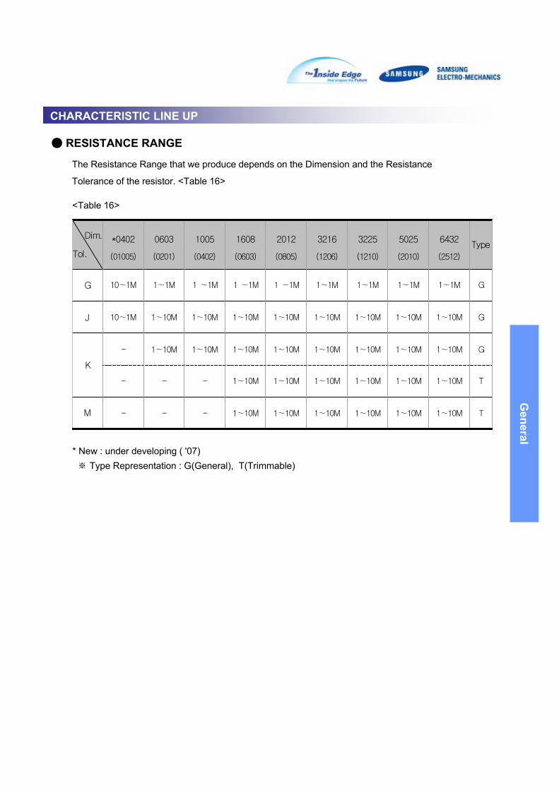
RESISTANCE RANGE
The Resistance Range that we produce depends on the Dimension and the Resistance
Tolerance of the resistor. <Table 16>
<Table 16>
Dim.
Tol.
*0402 0603 1005 1608 2012 3216 3225 5025 6432Type
(01005) (0201) (0402) (0603) (0805) (1206) (1210) (2010) (2512)
G 10∼1M 1∼1M 1 ∼1M 1 ∼1M 1 ∼1M 1∼1M 1∼1M 1∼1M 1∼1M G
J 10∼1M 1∼10M 1∼10M 1∼10M 1∼10M 1∼10M 1∼10M 1∼10M 1∼10M G
K
- 1∼10M 1∼10M 1∼10M 1∼10M 1∼10M 1∼10M 1∼10M 1∼10M G
- - - 1∼10M 1∼10M 1∼10M 1∼10M 1∼10M 1∼10M T
M - - - 1∼10M 1∼10M 1∼10M 1∼10M 1∼10M 1∼10M T
* New : under developing ( '07)※ Type Representation : G(General), T(Trimmable)
General
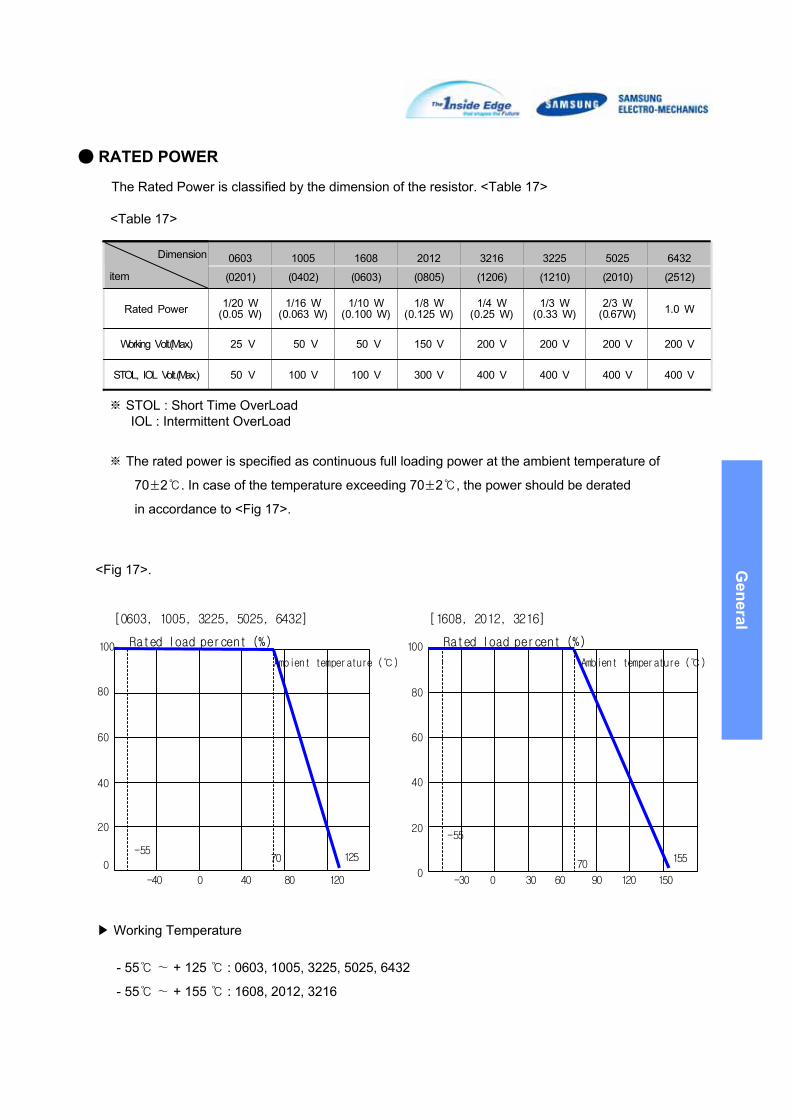
<Fig 17>.
Working Temperature
Ambient temperature ()
100
80
40
60
20
0
-55
0 30 60 90 150120
15570
-30
100
80
40
60
20
0
-55
0 40 80 120
125
Ambient temperature ()
-40
70
Rated load percent (%) Rated load percent (%)
[1608, 2012, 3216][0603, 1005, 3225, 5025, 6432]
- 55∼ + 125 : 0603, 1005, 3225, 5025, 6432
- 55∼ + 155 : 1608, 2012, 3216
RATED POWER
The Rated Power is classified by the dimension of the resistor. <Table 17>
<Table 17>
Dimension
item0603 1005 1608 2012 3216 3225 5025 6432
(0201) (0402) (0603) (0805) (1206) (1210) (2010) (2512)
Rated Power 1/20 W(0.05 W)
1/16 W(0.063 W)
1/10 W(0.100 W)
1/8 W(0.125 W)
1/4 W(0.25 W)
1/3 W(0.33 W)
2/3 W(0.67W) 1.0 W
Working Volt.(Max.) 25 V 50 V 50 V 150 V 200 V 200 V 200 V 200 V
STOL, IOL Volt.(Max.) 50 V 100 V 100 V 300 V 400 V 400 V 400 V 400 V
※ STOL : Short Time OverLoadIOL : Intermittent OverLoad
※ The rated power is specified as continuous full loading power at the ambient temperature of
70±2. In case of the temperature exceeding 70±2, the power should be derated
in accordance to <Fig 17>.
General
RELIABILITY TEST CONDITIONJumper's reliability test data are only applied to General type resistor.
ELECTRICAL CHARACTERISTICThe electrical characteristic test should satisfy the test method, procedure, and standard.
If there is no special comment, Each test performs in standard state.
(temperature 20, humidity 65%RH, pressure 1023mbar)
itemPermissible deviation
Test methodResistor Jumper
DC resistance
DC resistance value
should be within the
specified resistance
tolerance.
50mΩ
Maximum
묤 Standard : JIS C 5201-1 4.5묤 Test voltage : <Table 8>묤 Applying time : within 5 seconds.묤 Test board : <Fig 11>
Temperature
Coefficient
of
Resistance
-
묤 Standard : JIS C 5201-1 4.8묤 Temp. : 20 → -55 → 20 → 125 →
20
묤 Test board : <Fig 13>묤 Calculation :
TCR(ppm/) =
T0 : 20 ± 2
R0 : Resistance at T0 (Ω)
T : Test temperature ( -55, 125)
R : Resistance at T (Ω)
Short time
overload
(STOL)
1. No mechanical
damage
2. ΔR should be
within ±(1%+0.1Ω)
50mΩ
Maximum
묤 Standard : JIS C 5201-1 4.13묤 Test voltage : 2.5 times of rated voltage Max.
surge current at the Jumper.묤 Applying time : 5 seconds묤 Test board : <Fig 12>
Intermittent
overload(IOL)
1. No mechanical
damage
2. ΔR should bewithin ±(3%+0.1Ω)
50mΩ
Maximum
묤 Standard : JIS C 5201-1 4.13묤 Test voltage : 2.5 times of rated voltage Max.
surge current at the Jumper.묤 Test method : 1 sec ON, 25 sec OFF
10,000+40 0cycles묤 Test board : <Fig 12>
<Table 8>
Range (Ω) Voltage (V)1≤ R < 10 0.1
10 ≤ R < 100 0.3100 ≤ R < 1K 1.01K ≤ R < 10K 3.0
10K ≤ R < 100K 10.0100K ≤ R < 1M 25.0
1M ≤ R < 10M 30.0
Range(Ω) ppm/1 ≤ R < 10 ±500
10 ≤ R < 1M ±2000603:±250
1M ≤ R < 10M ±300
R RR T T−
×−
×0
0 0
6110
<Table 9>
General
MECHANICAL CHARACTERISTIC
itemPermissible deviation
Test methodResistor Jumper
Withstanding
voltage
묤 No mechanical
damage, short circuit,
or disconnection.
Same as
left
묤 Standard : JIS C 5201-1 4.7묤 Test voltage : 0603,1005,1608 AC 100V,
others AC 500V묤 Applying time : 60 +10/-0 seconds묤 Test board : <Fig 13>
Insulation
resistance
묤 Should have more
than 1,000MΩ
Same as
left
묤 Standard : JIS C 5201- 4.7묤 Test voltage : 0603,1005,1608 DC 100V,
others DC 500V묤 Applying time : 60 seconds묤 Test pressure : 1.0±0.2 N묤 Test board : <Fig 13>
Noise
묤 Noise standard
<Table 10>
-
묤 Measure equipment : QUAN-TECH NOISE
METER
(MODEL 315C)
Range (Ω) dB Max.1 ≤ R < 100 -10
100 ≤ R < 1K 01K ≤ R < 100K 15
100K ≤ R < 1M 201M ≤ R < 10M 30
The mechanical characteristic test should satisfy the test method, procedure, and standard.If there is no special comment, each test is performed at standard conditions. (temperature 20, humidity 65%RH, pressure 1023mbar)
itemPermissible deviation
Test methodResistor Jumper
Solderability
묤 New solder
coated more than
95% of termination
Same as
left
묤 Standard : JIS C 5201-1 4.17묤 Test temperature : 245 ± 5
묤 Test time : 3 ± 0.5 sec (dipping both side)
Bendingstrength
1. No mechanical
damage2. ΔR should be
within ±(0.5%+0.05Ω)
Same asleft
묤 Standard : JIS C 5201-1 4.33묤 Test board : <Fig 12>묤 Test speed : 100mm/min묤 Test procedure : press until 3mm,
then keep 5 seconds <Fig 14>
20R205
3
<Fig 14>
0603:±(1.0%+0.1%)
General
ENVIRONMENTAL CHARACTERISTICThe Environmental characteristic test should satisfy the test method, procedure, and standard.
If there is no special comment, Each test performs in standard state.
(temperature 20, humidity 65%RH, pressure 1023mbar)
itemPermissible deviation
Test methodResistor Jumper
Termination
strength
묤 No mechanicaldamage, or sign of
disconnection
Same as
left
묤 Standard : JIS C 5201-1 4.16묤 Test time : applying pressure for 10 seconds묤 Test tension : 0603,1005,1608 - 3N (300g묤f)
Others (500g묤f)
Withstandingsoldering heat
1. No mechanical
damage2. ΔR should be
within ±(1%+0.05Ω)
50mΩ
Maximum
묤 Standard : JIS C 5201-1 4.18묤 Temperature : 260 ± 5묤 Test time : 10 ± 1second (both side dipping)묤 Test procedure : measures after 24 hours
Vibration
1. No mechanical
damage2. ΔR should be
within ±(1%+0.05Ω)
50mΩ
Maximum
묤 Standard : JIS C 5201-1 4.22묤 Test amplitude : 1.5mm묤 Test procedure : frequency 10Hz - 55Hz -
10Hz each 2 hours in x, y, z direction.
itemPermissible deviation
Test methodResistor Jumper
Temperature
cycle
1. No mechanicaldamage
2. ΔR should bewithin ±(1%+0.1Ω)
50mΩ
Maximum
묤 Standard : JIS C 5201-1 4.19묤 Test procedure : <Table 11>묤 Measure : after 100 cycles of procedure묤 Test board : <Fig 11>
Moisture
resistance life
1. No mechanicaldamage
2. ΔR should bewithin <Table 12> 50mΩ
Maximum
묤 Standard : JIS C 5201-1 4.14묤 Test condition : temp 40 ± 3, humid 90 ~
95%RH묤 Test voltage : rated voltage묤 Test time : repeat 90min ON, 30min OFF
during 1000+4 8 hours묤 Test board : <Fig 11>
item 1 2 3 4temp() -55±2 5~35 125±2 5~35time(min) 30 15 30 15
<Table 11>
<Table 12>Range(Ω) ΔR MAX
1 ≤ R < 10 ±5%10 ≤ R < 1M ±(3%+0.1Ω)
1M ≤ R < 10M ±5%
General
TEST BOARD AND SPECIFICATION
Soldering (for lead free type)
▷ The resistor should be fixed on PCB(printed circuit board) for testing.
- Soldering specification : JIS C 5201-1 4.18
* Soldering method : Flow type (Dipping type)
* Solder : Sn -3.0 Ag -0.5 Cu
* FLUX : ROSIN 25WT% (JIS K 5902), IPA 75WT% (JIS K 5901)
- Flow soldering condition
* FLUX dipping time : 5∼10 sec
* Pre-treatment : None
* Soldering temp : 260±5
* Soldering time : 10±1 sec
itemPermissible deviation
Test methodResistor Jumper
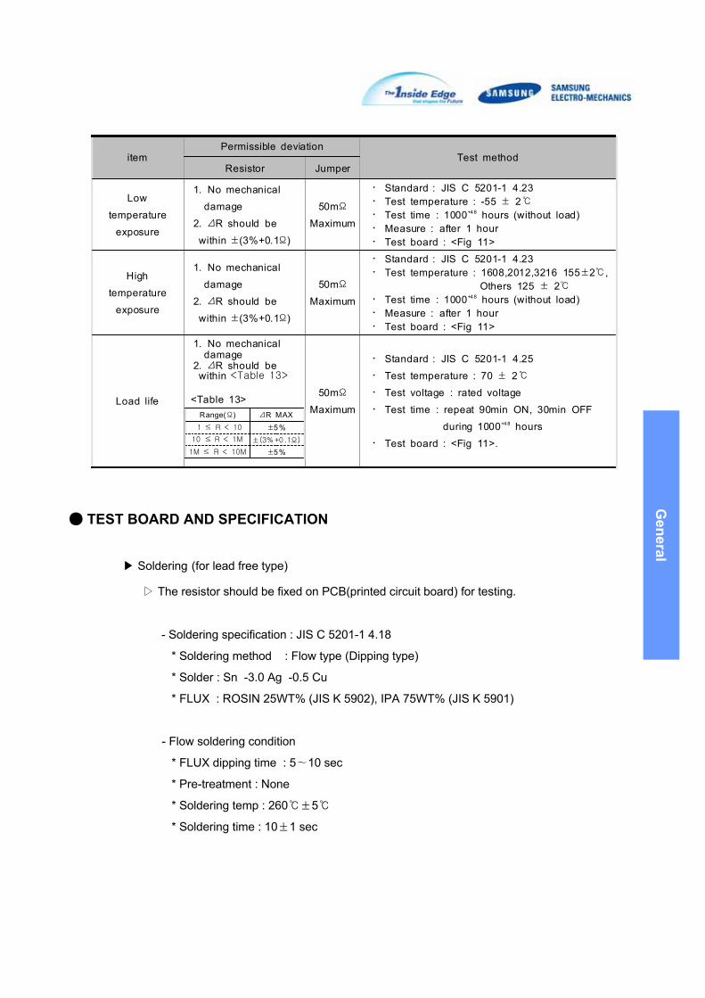
Low
temperature
exposure
1. No mechanicaldamage
2. ΔR should be
within ±(3%+0.1Ω)
50mΩ
Maximum
묤 Standard : JIS C 5201-1 4.23묤 Test temperature : -55 ± 2묤 Test time : 1000+48 hours (without load)묤 Measure : after 1 hour묤 Test board : <Fig 11>
High
temperature
exposure
1. No mechanical
damage
2. ΔR should be
within ±(3%+0.1Ω)
50mΩ
Maximum
묤 Standard : JIS C 5201-1 4.23묤 Test temperature : 1608,2012,3216 155±2,
Others 125 ± 2묤 Test time : 1000+48 hours (without load)묤 Measure : after 1 hour묤 Test board : <Fig 11>
Load life
1. No mechanicaldamage
2. ΔR should bewithin <Table 13>
50mΩ
Maximum
묤 Standard : JIS C 5201-1 4.25묤 Test temperature : 70 ± 2
묤 Test voltage : rated voltage묤 Test time : repeat 90min ON, 30min OFF
during 1000+4 8 hours묤 Test board : <Fig 11>.
<Table 13>Range(Ω) ΔR MAX
1 ≤ R < 10 ±5%10 ≤ R < 1M ±(3%+0.1Ω)
1M ≤ R < 10M ±5%
General
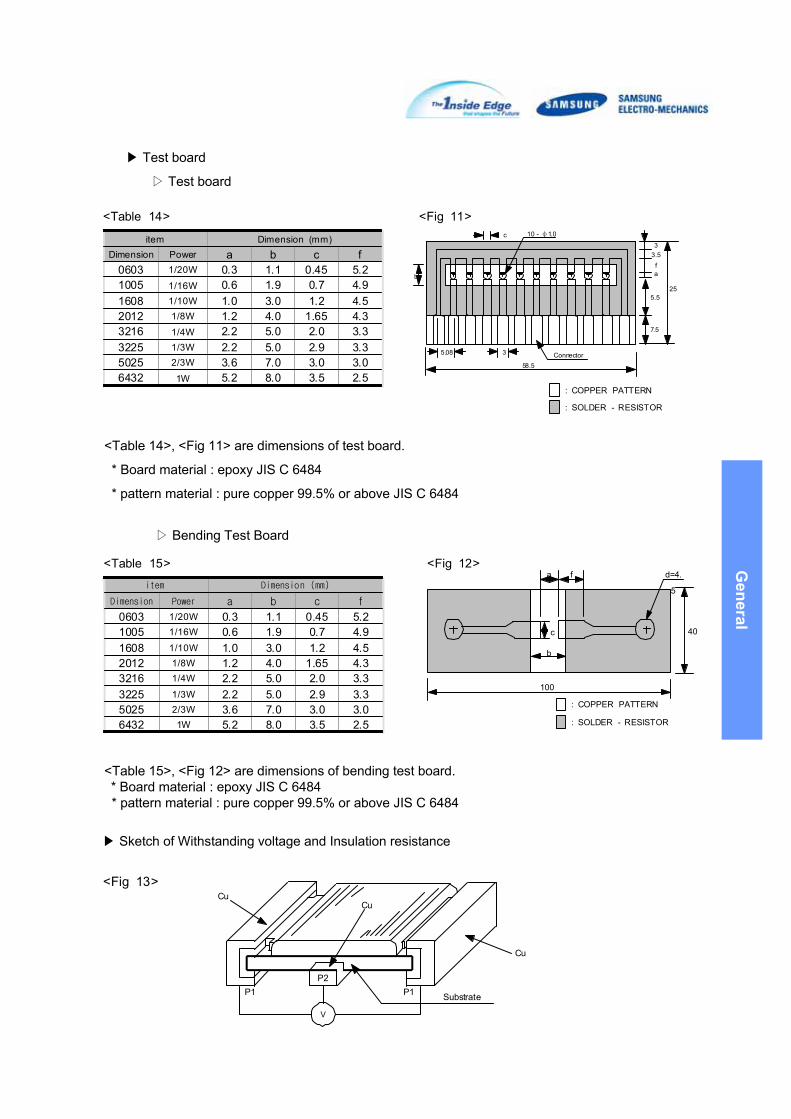
▷ Bending Test Board
Sketch of Withstanding voltage and Insulation resistance
Test board
▷ Test board
<Table 14>, <Fig 11> are dimensions of test board.
* Board material : epoxy JIS C 6484
* pattern material : pure copper 99.5% or above JIS C 6484
<Table 15>, <Fig 12> are dimensions of bending test board.* Board material : epoxy JIS C 6484* pattern material : pure copper 99.5% or above JIS C 6484
P2P1P1
V
Substrate
Cu
CuCu
<Fig 13>
<Fig 11>
item Dimension (mm)Dimension Power a b c f
0603 1/20W 0.3 1.1 0.45 5.21005 1/16W 0.6 1.9 0.7 4.91608 1/10W 1.0 3.0 1.2 4.52012 1/8W 1.2 4.0 1.65 4.33216 1/4W 2.2 5.0 2.0 3.33225 1/3W 2.2 5.0 2.9 3.35025 2/3W 3.6 7.0 3.0 3.06432 1W 5.2 8.0 3.5 2.5
<Table 14>
58.5Connector35.08
b
c 10 - φ1.0
7.5
5.5
af
3.53
25
: COPPER PATTERN
: SOLDER - RESISTOR
<Fig 12>
b
a f d=4.
5
40c
100
<Table 15>
item Dimension (mm)
Dimension Power a b c f
0603 1/20W 0.3 1.1 0.45 5.21005 1/16W 0.6 1.9 0.7 4.91608 1/10W 1.0 3.0 1.2 4.52012 1/8W 1.2 4.0 1.65 4.33216 1/4W 2.2 5.0 2.0 3.33225 1/3W 2.2 5.0 2.9 3.35025 2/3W 3.6 7.0 3.0 3.06432 1W 5.2 8.0 3.5 2.5
: COPPER PATTERN
: SOLDER - RESISTOR
General
RELIABILITY TEST CONDITION
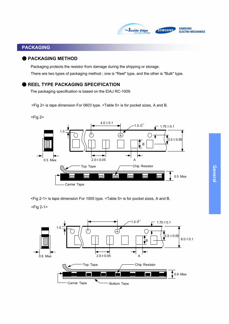
PACKAGING METHOD
RELIABILITY TEST CONDITIONPACKAGING
REEL TYPE PACKAGING SPECIFICATION
<Fig 2-1>
PACKAGING
<Fig 2>
Packaging protects the resistor from damage during the shipping or storage.
There are two types of packaging method ; one is "Reel" type, and the other is "Bulk" type.
The packaging specification is based on the EIAJ RC-1009.
<Fig 2> is tape dimension For 0603 type. <Table 5> is for pocket sizes, A and B.
0.5 Max
1.0
2.0±0.05
4.0±0.1
A
B
1.5±0.10 1.75±0.1
3.5±0.05
0.5 Max
Chip ResistorTop Tape
Carrier Tape
<Fig 2-1> is tape dimension For 1005 type. <Table 5> is for pocket sizes, A and B.
0.6 Max
1.0
2.0±0.05 A
B
1.5±0.10 1.75±0.1
3.5±0.058.0±0.1
0.6 Max
Chip Resistor
Bottom Tape
Top Tape
Carrier Tape
General
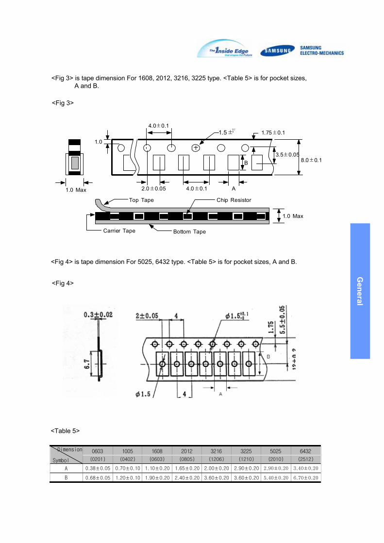
<Fig 3>
<Fig 3> is tape dimension For 1608, 2012, 3216, 3225 type. <Table 5> is for pocket sizes, A and B.
1.0 Max
1.0
2.0±0.05
4.0±0.1
4.0±0.1 A
B
1.5±0.10 1.75±0.1
3.5±0.058.0±0.1
1.0 Max
Chip Resistor
Bottom Tape
Top Tape
Carrier Tape
<Fig 4> is tape dimension For 5025, 6432 type. <Table 5> is for pocket sizes, A and B.
<Fig 4>
Dimension
Symbol
0603 1005 1608 2012 3216 3225 5025 6432
(0201) (0402) (0603) (0805) (1206) (1210) (2010) (2512)
A 0.38±0.05 0.70±0.10 1.10±0.20 1.65±0.20 2.00±0.20 2.90±0.20 2.90±0.20 3.40±0.20
B 0.68±0.05 1.20±0.10 1.90±0.20 2.40±0.20 3.60±0.20 3.60±0.20 5.40±0.20 6.70±0.20
<Table 5>
General
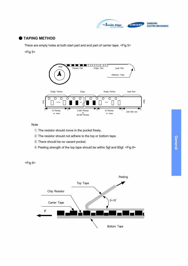
TAPING METHOD
There are empty holes at both start part and end part of carrier tape. <Fig 5>
<Fig 5>
ReelPacked Part Empty Part Lead Part
Adhesion Tape
*********
Start
Empty Portion Chips Empty Portion Lead Part
10 Pitchesor more
End
5,000 Pitchesor
20,000 Pitches
10 Pitchesor more
200~250 mm
Note
① The resistor should move in the pocket freely.
② The resistor should not adhere to the top or bottom tape.
③ There should be no vacant pocket.
④ Peeling strength of the top tape should be within 5gf and 80gf. <Fig 6>
<Fig 6>
0~10°
Top Tape
Chip Resistor
Carrier Tape
Bottom Tape
F
Peeling
General
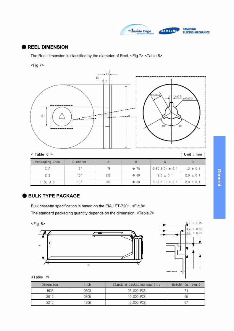
REEL DIMENSION REEL DIMENSION
The Reel dimension is classified by the diameter of Reel. <Fig 7> <Table 6>
<Fig 7>
BULK TYPE PACKAGE
Bulk cassette specification is based on the EIAJ ET-7201. <Fig 8>
The standard packaging quantity depends on the dimension. <Table 7>
12
36
110
<Fig 8> 6.0 ± 0.05
4.4 ± 0.05
3.4 ± 0.05
<Table 7>
Dimension Inch Standard packaging quantity Weight (g, avg.)
1608 0603 25,000 PCS 71
2012 0805 10,000 PCS 65
3216 1206 5,000 PCS 67
Packaging Code Diameter A B C D
C S 7" 178 Φ 70 9.5(13.0) ± 0.1 1.2 ± 0.1
E S 10" 258 Φ 80 9.5 ± 0.1 2.0 ± 0.1
F S, A S 13" 330 Φ 80 9.5(13.0) ± 0.1 2.0 ± 0.1
[ Unit : mm ]< Table 6 >
General
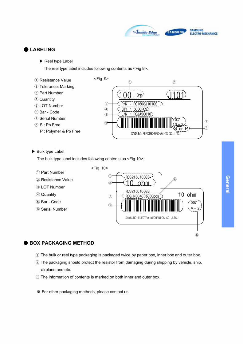
LABELING
BOX PACKAGING METHOD
Reel type Label
The reel type label includes following contents as <Fig 9>.
Bulk type Label
The bulk type label includes following contents as <Fig 10>.
① Part Number
② Resistance Value
③ LOT Number
④ Quantity
⑤ Bar - Code
⑥ Serial Number
<Fig 10>
RC3216J100GSROGHN0040 5000pcs 10 ohm
007
SAMSUNG ELECTRO-MECHANICS CO.,LTD.
RC3216J100GS
10 ohm
V - 2
①
②
③
④
⑤
⑥
① The bulk or reel type packaging is packaged twice by paper box, inner box and outer box.
② The packaging should protect the resistor from damaging during shipping by vehicle, ship,
airplane and etc.
③ The information of contents is marked on both inner and outer box.
※ For other packaging methods, please contact us.
① Resistance Value② Tolerance, Marking③ Part Number④ Quantity⑤ LOT Number⑥ Bar - Code⑦ Serial Number⑧ S : Pb Free
P : Polymer & Pb Free
②①<Fig 9>
100 J101Ohm
P/N : RC1608J101CS
QTY : 5000PCSL/N : ROJA50010
007
SAMSUNG ELECTRO-MECHANICS CO.,LTD.
Q - 2
④
③
⑤
⑥ ⑦
S or P ⑧
General
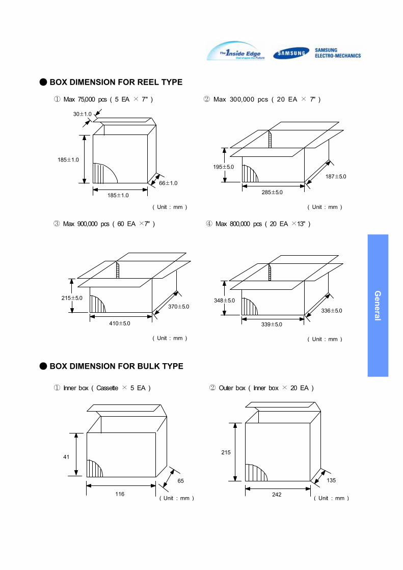
BOX DIMENSION FOR REEL TYPE
① Max 75,000 pcs ( 5 EA × 7" ) ② Max 300,000 pcs ( 20 EA × 7" )
( Unit : mm ) ( Unit : mm )
③ Max 900,000 pcs ( 60 EA ×7" ) ④ Max 800,000 pcs ( 20 EA ×13" )
( Unit : mm ) ( Unit : mm )
30±1.0
185±1.0
185±1.0
66±1.0
195±5.0
285±5.0
187±5.0
215±5.0
410±5.0
370±5.0348±5.0
339±5.0
336±5.0
BOX DIMENSION FOR BULK TYPE
① Inner box ( Cassette × 5 EA ) ② Outer box ( Inner box × 20 EA )
41
116
65
( Unit : mm ) 242
135
215
( Unit : mm )
Chip R
esistor
APPLICATION MANUAL
APPLICATIONS
Chip resistors are designed for general electronic devices such as home appliances, computer,
mobile communications, digital circuit, etc.
If you require our products with high reliability-performing at more than 125C or below -55C
for medical equipments, aircraft, high speed machines, military usage, and items that can
affect human life or if you need to use in specific conditions (corrosive gas atmosphere),
please contact us beforehand.
Normal Operation temperature ranges() as follows.
- 1608, 2012, 3216(general, precision) : -55 ~ + 155
- Others (rectangular, array, trimmable) : -55 ~ + 125
Although resistor body is coated, sharp excessive impact should be avoided to prevent
damages and adverse effects on characteristics(resistor value, open circuited, T.C.R.).
STORAGE
To maintain proper quality of chip components, the following precautions are required for storage environment, method and period.
Storage Environment
- Chip components may be deformed, if the temperature of packaged components exceeds
40.
- Do not store where the soldering properties can be deteriorated by harmful gas such as
sulphurous gas, chlorine gas, etc.
- Bulk packed chip components should be used as soon as the seal is opened, thus
preventing the solderability from deteriorating.
- The remaining unused chips should be put in the original bag and sealed again or store in
a desiccator containing a desiccating agent.
Storage Time Period
- Stored chip components should be used within 6 months after receiving the components.
If 6 months or more have elapsed, please check the solderability before actually using.
Chip R
esistor
MOUNTING
Our products have Ag electrodes protected by double layer.
1st Ni Coating
- This prevents Ag electrode from leaching and enhance the bonding with Sn
2nd Sn Coating
- This is made of Sn 100% with melting point 232 to prevent it from melting when solder
cream melts, and to enhance the bonding.
- Commercial solder creams are made of Sn-3.0Ag-0.5Cu with melting point 217.
CLEANING
CAUTION FOR CHIP RESISTOR SEPERATION FROM PCB
OTHERS
Proper nozzle height must be given attention so as not to give excessive pressure on the
chip during mounting on the PCB.
(Excessive pressure may cause exterior damage, change in resistance, circuit open, etc.)
If rosin flux is used, cleaning usually is unnecessary. When strongly activated flux is used, chlorine in the
flux may dissolve into some types of cleaning fluids, thereby affecting the chip capacitors.
This means that the cleaning fluid must be carefully selected, and should always be new.
PCB can be prevented from a shock because it has flexibility, but Chip resistor cannot : it is made of
ceramic, solder and metal.
Therefore, when separating Chip resistor from PCB, it is important for a chip not to be cracked.
Manual work
Manual soldering can pose a great risk of creating thermal cracks in chip resistors.
The hot soldering iron tip comes into direct contact with the end terminations, an operator's
carelessness may cause the tip of the soldering iron to come into direct contact with the
ceramic body of the resistor.
Therefore the soldering iron must be handled carefully, and close attention must be paid
to the selection of the soldering iron tip and to temperature control of the tip.
Do not use more than rated voltage.(check the contents on the file)
SOLDERING
Chip R
esistor
NOTICE
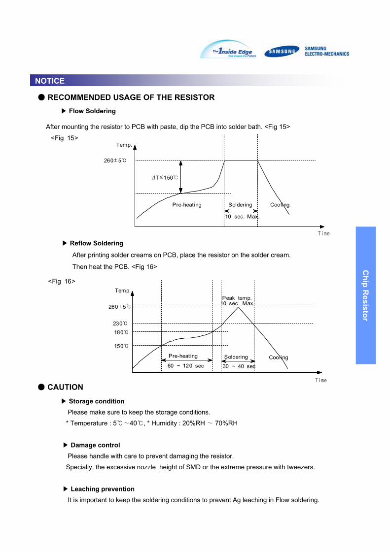
RECOMMENDED USAGE OF THE RESISTOR
Reflow Soldering
After printing solder creams on PCB, place the resistor on the solder cream.
Then heat the PCB. <Fig 16>
CAUTION
Flow Soldering
After mounting the resistor to PCB with paste, dip the PCB into solder bath. <Fig 15>
Storage conditionPlease make sure to keep the storage conditions.
* Temperature : 5∼40, * Humidity : 20%RH ∼ 70%RH
Damage controlPlease handle with care to prevent damaging the resistor.
Specially, the excessive nozzle height of SMD or the extreme pressure with tweezers.
Leaching preventionIt is important to keep the soldering conditions to prevent Ag leaching in Flow soldering.
<Fig 16>Temp.
Pre-heating Soldering Cooling60 ~ 120 sec
260±5
180
30 ~ 40 sec
230
150
Peak temp.10 sec. Max.
Time
<Fig 15>Temp.
Soldering Cooling
260±5
10 sec. Max.
Pre-heating
ΔT≤150
Time