Embed Size (px)
Citation preview
I
THE PENNSYLVANIA STATE UNIVERSITY
DEPARTMENT OF ENGINEERING SCIENCE AND MECHANICS
DETECTING DEFECTS IN CdTe SOLAR CELLS
USING EPR SPECTROSCOPY
LIAM A. YOUNG
Spring 2013
A thesis
submitted in partial fulfillment
of the requirements
for a baccalaureate degree
in Engineering Science
Reviewed and approved* by the following:
Patrick M. Lenahan
Distinguished Professor of Engineering Science
Thesis Supervisor
Bernhard R. Tittmann
Schell Professor of Engineering Science
Honors Adviser
Judith A. Todd
P. B. Breneman Deparment Head Chair
Professor, Department of Engineering Science and
Mechanics
* Signatures are on file in the Engineering Science and Mechanics office.
II
We approve the thesis of Liam A. Young:
Date of Signature
Patrick M. Lenahan
Distinguished Professor of Engineering Science
Thesis Supervisor
Bernhard R. Tittmann
Schell Professor of Engineering Science
Honors Adviser
Judith A. Todd
P. B. Breneman Department Head Chair
Professor, Department of Engineering Science
and Mechanics
Student ID# 911695783
III
Abstract
Cadmium telluride is a II-VI direct bandgap semiconductor with properties
conducive to becoming a photovoltaic cell. Recently, these compounds have been
researched as possible replacements for silicon based solar cells. With current
efficiencies much lower than anticipated, we assume that a defect in the compound is
causing electron mobility to decrease. In this study we will examine the CdTe samples
with Electron Paramagnetic Resonance spectroscopy at 300, 80, and 5 K.
IV
Table of Contents
List of Figures………………………………............................................................. V
Literature Review…………………………………………………………………... 1
Photovoltaics……………………………………………………………….... 1
EPR Spectroscopy…………………………………………………………... 4
Lab Configuration…………………………………………………………………... 7
Results………………………………………………………………………………... 11
Conclusions………………………………………………………………………….. 16
Future Work…………………………………………………………………………. 17
Appendix I…………………………………………………………………………… 19
Acknowledgments…………………………………………………………………… 20
Work Cited…………………………………………………………………………... 21
V
List of Figures
Figure 1: Shockley-Quisser Curve…………………………………………………..... 1
Figure 2: Direct and Indirect Band Gaps……………………………………………... 2
Figure 3: Superstrate CdTe Slar Cell………………………………………………..... 2
Figure 4: As-Deposited CdTe Device………………………………………………… 3
Figure 5: Post Pyrrole Treatment CdTe Device……………………………………..... 3
Figure 6: Magnetic Field Vs Energy………………………………………………….. 4
Figure 7: Simple EPR Signal………………………………………………………….. 5
Figure 8: Basic EPR Spectrometer……………………………………………………. 7
Figure 9: Insulated Dewars……………………………………………………………. 8
Figure 10: Liquid Helium System…………………………………………………...... 9
Figure 11: Cryostat Schematic………………………………………………………… 10
Figure 12: First CdTe Signal. 50K…………………………………………………..... 12
Figure 13: Spectral Comparison. 5K………………………………………………….. 13
Figure 14: CdTe + Cu. Calculating g………………………………………………….. 14
1
Literature Review
Photovoltaics
Photovoltaic (PV) cells are slowly becoming a large percentage of our nation’s
power supply. With the increasing needs of electricity, it is a high priority to find cleaner
sources of energy without creating too much cost. For solar cells to be more cost
effective, we must increase their efficiencies and lower their production expenses.
A solar panel is essentially little more than a p-n junction that absorbs light. Light
of a specific wavelength enters the cell and excites an electron. This electron is moved to
the conduction band where it escapes into a biased n-doped region. These escaped
electrons then become a current [18].
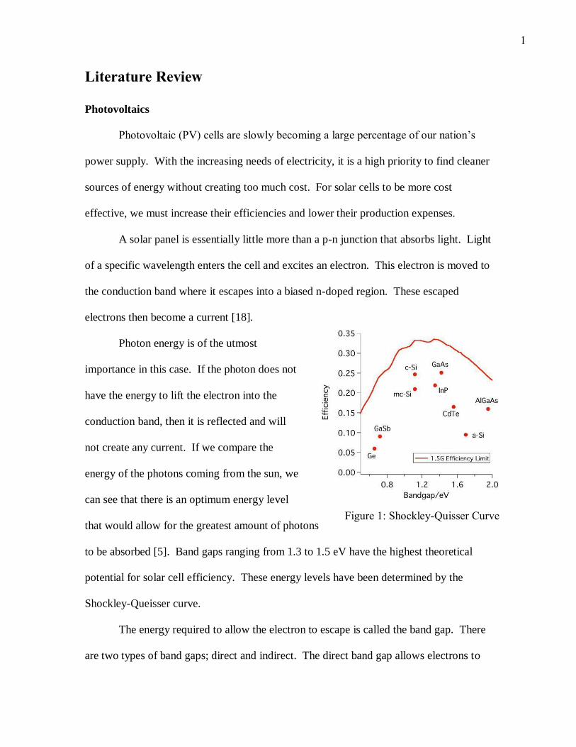
Photon energy is of the utmost
importance in this case. If the photon does not
have the energy to lift the electron into the
conduction band, then it is reflected and will
not create any current. If we compare the
energy of the photons coming from the sun, we
can see that there is an optimum energy level
that would allow for the greatest amount of photons
to be absorbed [5]. Band gaps ranging from 1.3 to 1.5 eV have the highest theoretical
potential for solar cell efficiency. These energy levels have been determined by the
Shockley-Queisser curve.
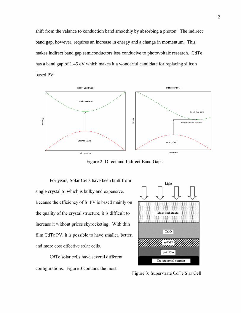
The energy required to allow the electron to escape is called the band gap. There
are two types of band gaps; direct and indirect. The direct band gap allows electrons to
Figure 1: Shockley-Quisser Curve
2
shift from the valance to conduction band smoothly by absorbing a photon. The indirect
band gap, however, requires an increase in energy and a change in momentum. This
makes indirect band gap semiconductors less conducive to photovoltaic research. CdTe
has a band gap of 1.45 eV which makes it a wonderful candidate for replacing silicon
based PV.
For years, Solar Cells have been built from
single crystal Si which is bulky and expensive.
Because the efficiency of Si PV is based mainly on
the quality of the crystal structure, it is difficult to
increase it without prices skyrocketing. With thin
film CdTe PV, it is possible to have smaller, better,
and more cost effective solar cells.
CdTe solar cells have several different
configurations. Figure 3 contains the most
Figure 2: Direct and Indirect Band Gaps
Figure 3: Superstrate CdTe Slar Cell
3
common form in which the cell is constructed on top of a glass substrate and then flipped
for actual function [2]. The fist layer is built from a transparent conducting oxide (TCO)
which allows light through to the junction and acts as the front contact. The CdS and
CdTe act as the n and p doped junction and are loaded with electrons and holes
respectively. Pure CdTe single crystals have a carrier concentration of about
[8]. These middle sections are built with chemical bath deposition (CBD)
which has creates efficiencies upwards of 16% [9]. The final layer is the back contact
that allows for current to flow.
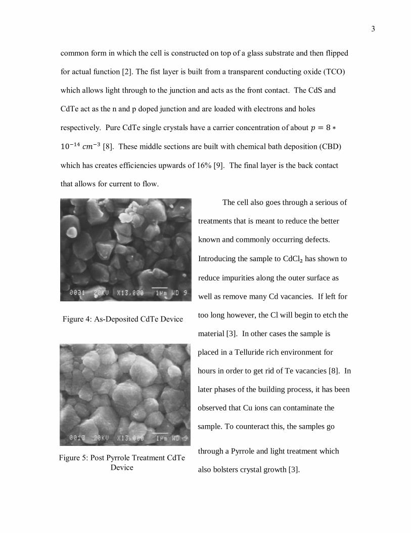
The cell also goes through a serious of
treatments that is meant to reduce the better
known and commonly occurring defects.
Introducing the sample to CdCl₂ has shown to
reduce impurities along the outer surface as
well as remove many Cd vacancies. If left for
too long however, the Cl will begin to etch the
material [3]. In other cases the sample is
placed in a Telluride rich environment for
hours in order to get rid of Te vacancies [8]. In
later phases of the building process, it has been
observed that Cu ions can contaminate the
sample. To counteract this, the samples go
through a Pyrrole and light treatment which
also bolsters crystal growth [3].
Figure 4: As-Deposited CdTe Device
Figure 5: Post Pyrrole Treatment CdTe
Device
4
EPR Spectroscopy
Electron Paramagnetic Resonance (EPR) Spectroscopy is a sensitive and accurate
tool for viewing structural defects in semiconductors and other materials. This technique
functions by creating a large magnetic field through the sample. This overpowering field
lines up electrons which will spin either with the field (low energy) or against the field
(high energy). By creating this new energy difference, we can examine patterns through
the electrons’ behavior. While inducing the magnetic field, we exposed the sample to
high energy microwaves. The photons will react with electrons which will then flip their
spins. By measuring the number of flips from low to high energy levels, we get what is
called an absorption spectrum.
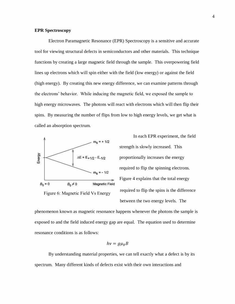
In each EPR experiment, the field
strength is slowly increased. This
proportionally increases the energy
required to flip the spinning electrons.
Figure 4 explains that the total energy
required to flip the spins is the difference
between the two energy levels. The
phenomenon known as magnetic resonance happens whenever the photons the sample is
exposed to and the field induced energy gap are equal. The equation used to determine
resonance conditions is as follows:
By understanding material properties, we can tell exactly what a defect is by its
spectrum. Many different kinds of defects exist with their own interactions and
Figure 6: Magnetic Field Vs Energy
5
idiosyncrasies. Due to EPR’s relatively extensive use, hundreds of these unique spectra
have already been analyzed and cataloged. The trouble lies mostly in being able to
identify the acquired spectrum and matching it to known samples.
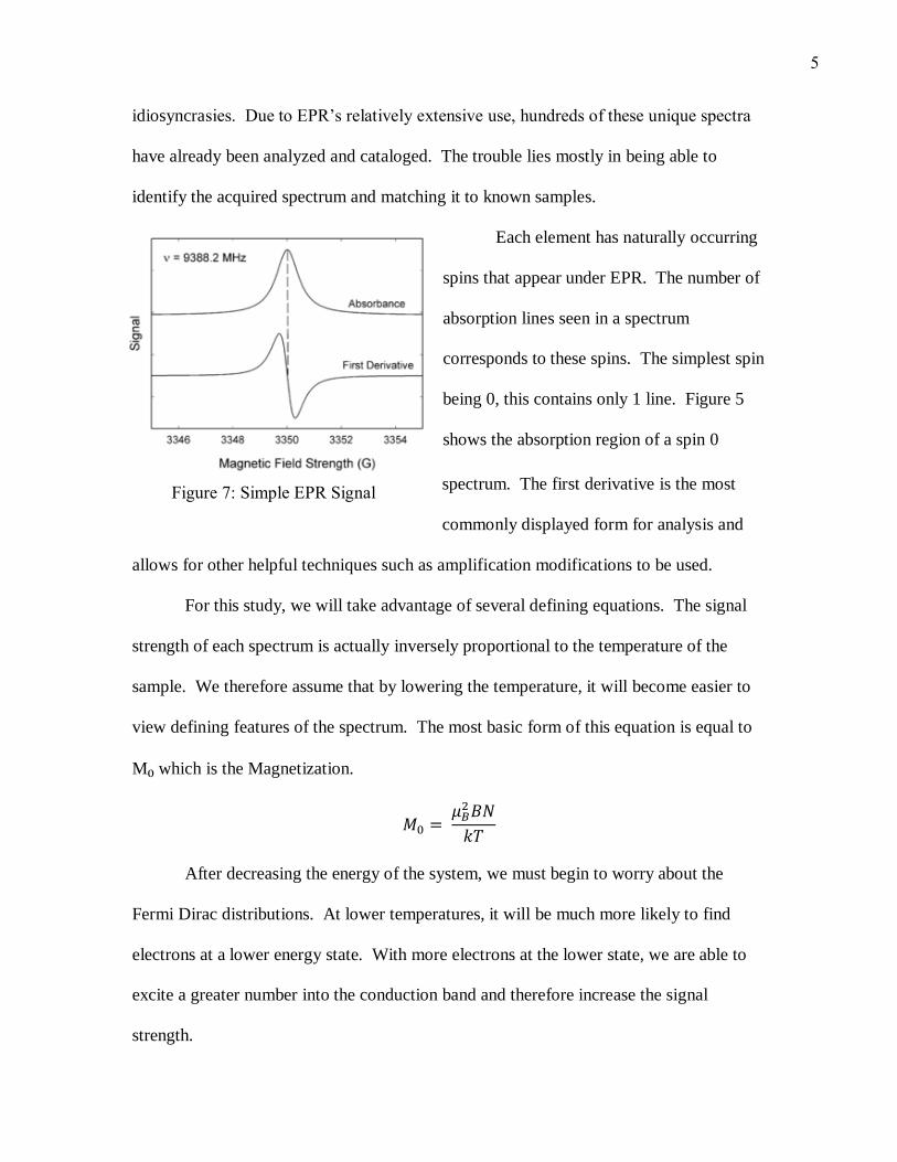
Each element has naturally occurring
spins that appear under EPR. The number of
absorption lines seen in a spectrum
corresponds to these spins. The simplest spin
being 0, this contains only 1 line. Figure 5
shows the absorption region of a spin 0
spectrum. The first derivative is the most
commonly displayed form for analysis and
allows for other helpful techniques such as amplification modifications to be used.
For this study, we will take advantage of several defining equations. The signal
strength of each spectrum is actually inversely proportional to the temperature of the
sample. We therefore assume that by lowering the temperature, it will become easier to
view defining features of the spectrum. The most basic form of this equation is equal to
M₀ which is the Magnetization.
After decreasing the energy of the system, we must begin to worry about the
Fermi Dirac distributions. At lower temperatures, it will be much more likely to find
electrons at a lower energy state. With more electrons at the lower state, we are able to
excite a greater number into the conduction band and therefore increase the signal
strength.
Figure 7: Simple EPR Signal
6
The tests will be run at 300 K, 80 K, 50 K, and 5 K. By decreasing the
temperature from 300 K to 5 K, we can theoretically increase the signal strength by a
factor of 60. 300K is the approximate room temperature of the lab in which the tests are
run. 80 K is the approximate temperature of the sample after being inserted into a liquid
nitrogen Dewar. 50 K and 5 K will be achieved through the use of a Janis Cryostat
system.
The spectrometer consists mainly of two large electromagnets, a microwave
bridge, and a microwave cavity. The magnets control the large field that forces the
electrons into order. These experiments are run at a magnetic field strength of 3400
Gauss (340 mT). The microwave bridge contains a Gunn oscillator which emits
microwaves between 9 and 10 GHz. These travel down to the cavity which is where the
sample is located. The cavity contains a standing wave and must be tuned by the
operator before every use. Improper tuning can lead to damage as seen during later
experimentation. Any photons not absorbed by the sample are reflected back and
counted.
7
Lab Configuration
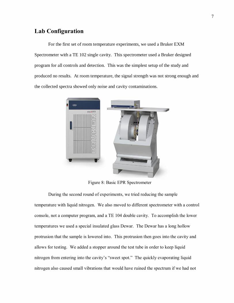
For the first set of room temperature experiments, we used a Bruker EXM
Spectrometer with a TE 102 single cavity. This spectrometer used a Bruker designed
program for all controls and detection. This was the simplest setup of the study and
produced no results. At room temperature, the signal strength was not strong enough and
the collected spectra showed only noise and cavity contaminations.
During the second round of experiments, we tried reducing the sample
temperature with liquid nitrogen. We also moved to different spectrometer with a control
console, not a computer program, and a TE 104 double cavity. To accomplish the lower
temperatures we used a special insulated glass Dewar. The Dewar has a long hollow
protrusion that the sample is lowered into. This protrusion then goes into the cavity and
allows for testing. We added a stopper around the test tube in order to keep liquid
nitrogen from entering into the cavity’s “sweet spot.” The quickly evaporating liquid
nitrogen also caused small vibrations that would have ruined the spectrum if we had not
Figure 8: Basic EPR Spectrometer
8
stabilized the sample with the stopper. We took the following steps to ensure that the
sample was and stayed cold for the entire experiment:
Fill the Dewar with liquid nitrogen and wait for the boiling to slow
Fill a cup with liquid nitrogen and place the sample inside to chill for 30 seconds
Empty out the Dewar making sure all the nitrogen has evaporated
Place the sample down into the Dewar and secure the stopper
Refill the Dewar with liquid nitrogen around the sample
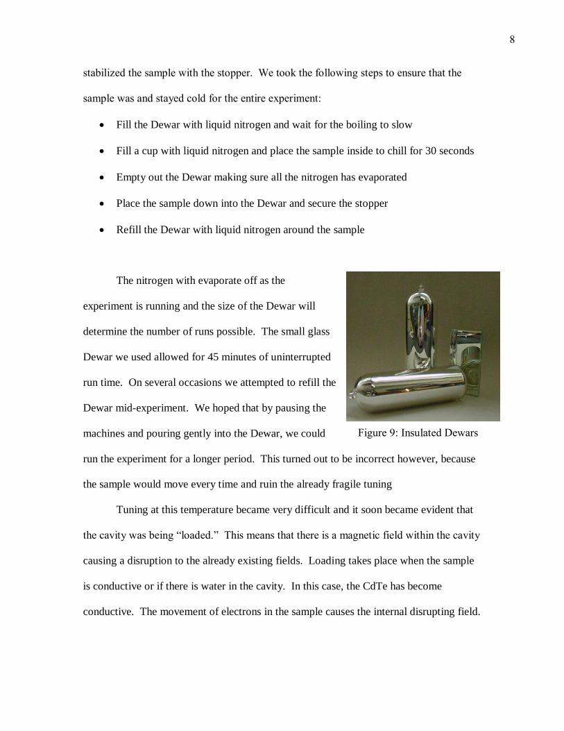
The nitrogen with evaporate off as the
experiment is running and the size of the Dewar will
determine the number of runs possible. The small glass
Dewar we used allowed for 45 minutes of uninterrupted
run time. On several occasions we attempted to refill the
Dewar mid-experiment. We hoped that by pausing the
machines and pouring gently into the Dewar, we could
run the experiment for a longer period. This turned out to be incorrect however, because
the sample would move every time and ruin the already fragile tuning
Tuning at this temperature became very difficult and it soon became evident that
the cavity was being “loaded.” This means that there is a magnetic field within the cavity
causing a disruption to the already existing fields. Loading takes place when the sample
is conductive or if there is water in the cavity. In this case, the CdTe has become
conductive. The movement of electrons in the sample causes the internal disrupting field.
Figure 9: Insulated Dewars
9
In an attempt to properly tune the cavity, we turned the attenuation to 15 db. The
unstable loaded tuning at such a high power strained the microwave bridge. This
eventually became too much for the bridge and it broke down. After realizing our
mistake, we replaced the bridge and moved to liquid helium temperatures.
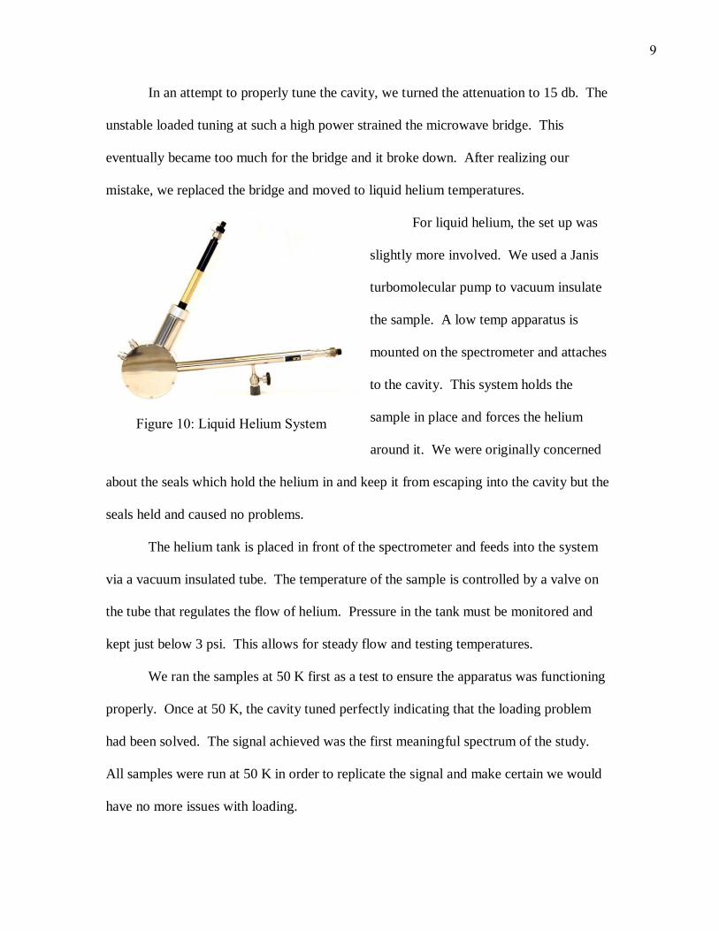
For liquid helium, the set up was
slightly more involved. We used a Janis
turbomolecular pump to vacuum insulate
the sample. A low temp apparatus is
mounted on the spectrometer and attaches
to the cavity. This system holds the
sample in place and forces the helium
around it. We were originally concerned
about the seals which hold the helium in and keep it from escaping into the cavity but the
seals held and caused no problems.
The helium tank is placed in front of the spectrometer and feeds into the system
via a vacuum insulated tube. The temperature of the sample is controlled by a valve on
the tube that regulates the flow of helium. Pressure in the tank must be monitored and
kept just below 3 psi. This allows for steady flow and testing temperatures.
We ran the samples at 50 K first as a test to ensure the apparatus was functioning
properly. Once at 50 K, the cavity tuned perfectly indicating that the loading problem
had been solved. The signal achieved was the first meaningful spectrum of the study.
All samples were run at 50 K in order to replicate the signal and make certain we would
have no more issues with loading.
Figure 10: Liquid Helium System
10
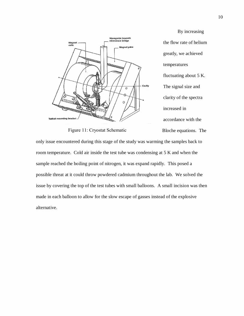
By increasing
the flow rate of helium
greatly, we achieved
temperatures
fluctuating about 5 K.
The signal size and
clarity of the spectra
increased in
accordance with the
Bloche equations. The
only issue encountered during this stage of the study was warming the samples back to
room temperature. Cold air inside the test tube was condensing at 5 K and when the
sample reached the boiling point of nitrogen, it was expand rapidly. This posed a
possible threat at it could throw powdered cadmium throughout the lab. We solved the
issue by covering the top of the test tubes with small balloons. A small incision was then
made in each balloon to allow for the slow escape of gasses instead of the explosive
alternative.
Figure 11: Cryostat Schematic
11
Results
The first round of texting took place at room temperature. Due to the relative size
of the defect, however, the spectra collected were meaningless. The background signal
was so large compared to the defect that even after several hundred runs and hours of
averaging there was no discernible data. Spectra for each sample varied due to noise
which caused random fluctuations in the signal.
Liquid nitrogen temperatures caused several unexpected problems. The reduction
in temperature should have produced a proportional increase in signal strength, but it
made the sample temporarily conductive. At 80 K, all the samples showed signs of
cavity loading caused by magnetic fields within the cavity. This in turn made tuning the
sample properly impossible. In our attempts to tune the cavity, the microwave bridge
was strained and began to malfunction. The AFC Lock-in had broken and the bridge was
unable to attain a signal even for weak pitch. Any and all data collected at this
temperature is meaningless due to the lack of control and damage done to the system.
Using liquid helium would increase the signal strength further by decreasing
temperature. The samples were chilled to 50 K as a test. It became immediately apparent
that the conductivity issue had been solved. The samples were able to tune perfectly
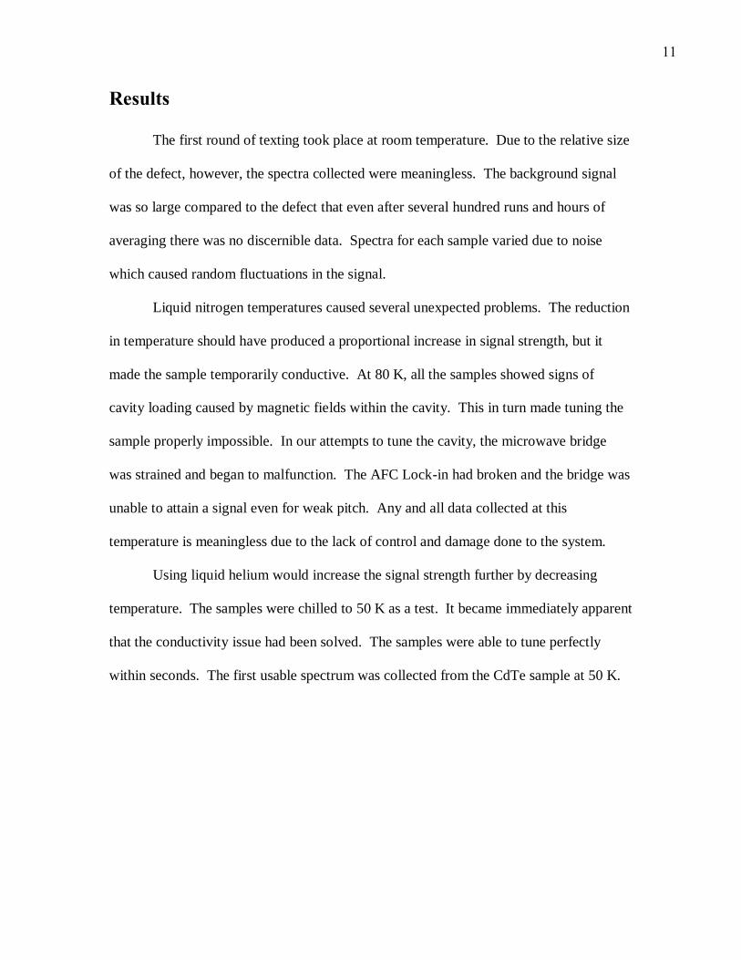
within seconds. The first usable spectrum was collected from the CdTe sample at 50 K.
12
We can see right away that the spectrum is dominated by a strong six line signal.
We interpret the six lines an element with a spin 5/2. This means that each line
corresponds to a directionality of spin for an electron on the defect. The other samples
showed similar signals with varying strengths. These variations are likely caused by
volume differences of each sample instead of a reduction in spins. By reducing the
temperature further, we can increase the defect signal again which will also raise the
single-to-noise ratio.
-0.80
-0.60
-0.40
-0.20
0.00
0.20
0.40
0.60
0.80
1.00
CdTe 50K
Figure 12: First CdTe Signal. 50K
13
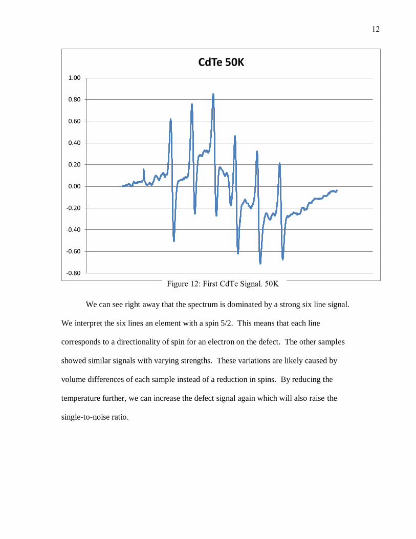
The spectrums collected at 5 K share the six line signal found at 50 K. By using a
table of spin constants, we can narrow down the element responsible for this defect. Due
to the strength of the six lines, we assume that the element is approximately 100% spin
5/2, meaning all of the natural isotopes match that spin. There are only four elements that
correspond to this spin ratio; aluminum, manganese, iodine, and praseodymium
We can rule out praseodymium immediately being that it is a lanthanide. To
narrow the possibilities down further, we examine the g values. The free electron g is
2.0023 and large atoms have larger g values. In this case, we have a center field of 3400
Gauss and the middle of the six lines is very well aligned with the center field. Al and
2650.00 2850.00 3050.00 3250.00 3450.00 3650.00 3850.00 4050.00
EPR
Am
plit
ud
e (
AU
)
Magnetic Field (Gauss)
CdTe
CdTe+CdCl2
CdTe+CdCl2
+Cu
CdTe+Cu
Figure 13: Spectral Comparison. 5K
14
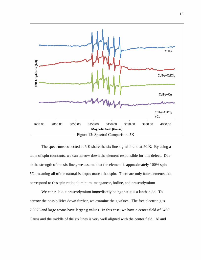
Mn are small enough to leave the spectrum close to the central field. We can calculate
the experimental g from the following graph.
To find g, we use the following equation that employs the range of the signal. By
taking B1 and B2, we calculate the center of the signal. We then find the percentage of
change from the original center field.
The g calculated comes out to be 2.011. According to another paper, Mn in CdTe
has a g value of 2.005. This difference however does not immediately exclude Mn as a
possibility. There is very little information on Al in CdTe and it is therefore hard to use g
to concretely determine if the impurity is Al or Mn. Mn however, is still much more
-0.20
-0.15
-0.10
-0.05
0.00
0.05
0.10
0.15
0.20
0.25
2,600.00 2,800.00 3,000.00 3,200.00 3,400.00 3,600.00 3,800.00 4,000.00 4,200.00
CdTe + Cu
B1
B2
Figure 14: CdTe + Cu. Calculating g
15
likely due to its use in other research areas it being seen in CdTe as an impurity before.
Al isn’t used in any treatments nor does it come in contact with the CdTe at any point
during construction of the Solar Cell. Because the CdTe of these samples was created
sterilely for this experiment, we can assume that it should not come in contact with any
Al. We deduce from this that Mn is the most likely impurity
16
Conclusions
After three round of experimentation, two of which were wildly unsuccessful, we
can see that the defect creates a six line signal with a g close to that of the free electron.
The functioning experiment being helium cooled samples at 50 K and below. At this
temperature we have increased the signal size enough to be detected and gotten rid of the
conductivity that caused loading.
By examining contemporary articles, we have determined that an interstitial
defect of Mn is the most likely culprit. There are several papers on Mn as an impurity of
CdTe and almost no information about Al. Our sponsor, GE, was very surprised by our
findings and was unsure of the defect’s origin. Other companies we work with, however,
have considered Mn as a possibility which only further supports our initial conclusion.
17
Future Work
To continue the work done during this study, we will examine the samples under
different conditions and using different techniques. To truly gauge the defect’s
interactions, we need to study a complete solar cell. This would allow for several tests
that could explain other aspects of the defect.
Cavity loading was an immense issue for this study and caused damage to one of
the systems. We will test the samples starting at room temperature and slowly lowering
them to 80 K. At some point the sample will become conductive and no longer function
in its intended manner. This will determine if CdTe based solar cells can be used in some
of the colder parts of the world.
Between 80 and 50 K, the sample became nonconductive and the charge carriers
would no longer move. Although this has no current use to us, this temperature and
phenomenon may apply to similar devices and may therefore be useful in the future. For
both the cavity loading and carrier freezeout experiments, we would use the Janis
temperature control system. This would allow for a steady drop in temperature while still
being capable of reaching carrier freezeout.
If the sample is a complete photovoltaic cell then we can test its functionality
while under observation. By applying light to a cell that is already undergoing EPR
spectroscopy, we might see how the hanging bond changes and interacts with other
electrons. We would run the sample at varying temperatures again however it is unlikely
to work at 50 K or below due to carrier freezout.
Under the six line signal is a very sizable amount of background and other
signals. They are much more difficult to see being that there is such a strong other signal.
18
If we could subtract the six lines away and leave everything else, we could see everything
in the sample. We have attempted to create an artificial six line signal from the original
signal but other factors came into play such as hyperfine interactions. These slightly
alter the signal and made the initial subtraction attempts useless. The program EasySpin,
which works through MATLAB, can simulate a much better signal. We should be able
to use EasySpin to build better spectral subtractions.
19
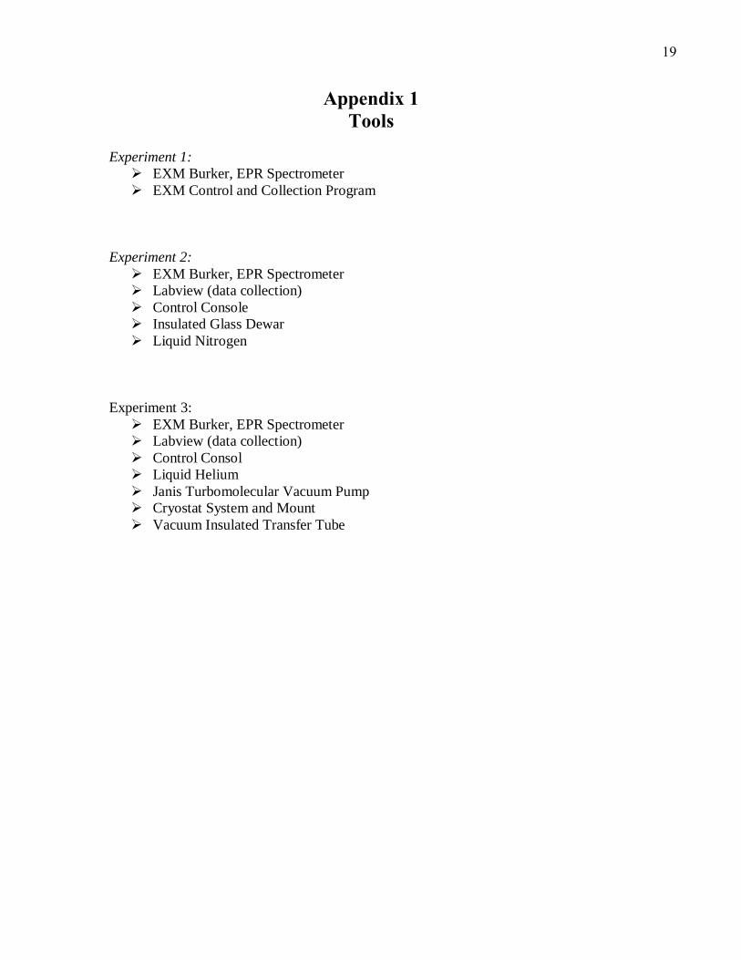
Appendix 1
Tools
Experiment 1:
EXM Burker, EPR Spectrometer
EXM Control and Collection Program
Experiment 2:
EXM Burker, EPR Spectrometer
Labview (data collection)
Control Console
Insulated Glass Dewar
Liquid Nitrogen
Experiment 3:
EXM Burker, EPR Spectrometer
Labview (data collection)
Control Consol
Liquid Helium
Janis Turbomolecular Vacuum Pump
Cryostat System and Mount
Vacuum Insulated Transfer Tube
20
Acknowledgements
I would first and foremost like to thank Dr. Lenahan who provided me with this
opportunity and showed the utmost patience during this project. Michael Pigott was the
best lab partner I could have asked for and I’m well aware that this project would not
have gone as smoothly without him. Corey Cochran, Tom Pomorski, Mike Mutch, Mark
Anders, and Jake Fulman who worked alongside us in the lab and were never too busy to
give a helping hand.
I would also like to thank my brothers who listened to hours of brain storming and
never once complained.
21
Work Cited
[1] Galazka, R. R. and Wojtowicz, T. (2010). CdTe and Related Compounds; Physics,
Defects, Hetero- and Nano-structures, Crystal Growth, Surfaces and Applications
[2] Compaan, A. and Bohn, R. (1992). Thin Film Cadmium Telluride Photovoltaic Cells,
Annual Subcontract Report. 23 July 1990 – 31 October 1991
[3] Koll, D. K., Taha, A. H., Giolando, D. M. (2011). Photochemical “Self-Healing”
Pyrrole Based Treatment of CdS/CdTe Photovoltaics. Solar Energy Materials and
Solar Cells, 95(7).
[4] Gessert, T. A. (2012). Cadmium Telluride Photovoltaic Thin Film: CdTe.
Comprehensive Renewable Energy, 423-438.
[5] Al-Dhafiri, A. M. (1998). Photovoltaic Properties of CdTe – Cu2Te. Renewable
Energy, 14(1-4).
[6] Chin, K. K. (2012). U.S. Cl. 136/260; 438/95; 257/E31.015. Washington, DC: U.S.
[7] Smith, L. C., Bingham, S. J., Davies, J. J., and Wolverson, D. (2005). Electron
Paramagnetic Resonance of Manganese Ions in CdTe Detected by Coherent
Raman Spectroscopy. Department of Physics, University of Bath, U.K.
[8] Emanuelsson, P., Omling, P., Meyer, B. K., Wienecke. M., and Schenk. M. (1993).
Identification of Cadmium Vacancy in CdTe by Electron Paramagnetic
Resonance. Physical Review, 47(13).
[9] Morales-Acevedo, A. (2006). Thin Film CdS/CdTe Solar Cells: Research
Perspectives. Solar Energy, 80(6).
[10] Lane, D. W., Rogers, K. D., Painter, J. D., Wood, D. A., and Ozsan, M. E. (2000).
Structural Dynamics in CdS-CdTe Thin Films. Thin Solid Films, 361-362.
22
[11] Schwartz, R. N., Wang, C., Trivedi, S., Jagannathan, G. V., Davidson, F. M., Boyd,
P. R., and Lee, U. (1997). Spectroscopic and Photorefractive Characteristics of
Cadmium Telluride Crystals Codoped with Vanadium and Manganese. Physical
Review, 55(23).
[12] Stefaniuk, I., Bester, M., Virt, I. S., and Kuzma, M. (2005). EPR Spectra of Cr in
CdTe Crystals. ACTA Physica Polonica A, 108(2).
[13] Pires, R. G., Dickstein, R. M., Titcomb, L. S., and Anderson, R. L. (1990). Carrier
Freezeout in Silicon. Cryogenics, 30(12).
[14] First Solar. (2011). First Solar Sets World Record for CdTe Solar PV Efficiency.
Available: http://investor.firstsolar.com/releasedetail.cfm?ReleaseID=593994.
[15] Eaton, G. R., Eaton, S. S., Barr, D. P., and Weber, R. T. (2010). Quantitative EPR.
Germany: Springer-Verlag/Wien.
[16] Dhere, R. G., Joel, N. D., DeHart, C. M., Li, J. V., Kuciauskas, D., and Gessert, T.
A. (2012). Development of Substrate Structure CdTe Photovoltaic Devices with
Performance Exceeding 10%. NREL. Golden CO, U.S.
[17] Lenahan, P. M. and Cochrane, C. J., (2013). A Brief Introduction to Electron Spin
Resonance. Unpublished Manuscript.
[18] Gessert, T. A. (2010). Junction Evolution During Fabrication of CdS/CdTe Thin-
film PV Solar Cells. NREL. Presented: 9-2010. China New Energy International
Forum and Fair.


![THESIS TITLE A THESIS SUBMITTED TO THE MIDDLE EAST ...ii.metu.edu.tr/system/files/documents/thesis... · [SAMPLE 1] Approval of the thesis: THESIS TITLE Submitted by STUDENT NAME](https://img.pdfslide.us/doc/110x75/6019035f39977162fc4f0b03/thesis-title-a-thesis-submitted-to-the-middle-east-iimetuedutrsystemfilesdocumentsthesis.jpg)