Embed Size (px)
Citation preview

Thermoelectric Figure of Merit of Degenerate and Nondegenerate Semiconductors
A Dissertation Presented
by
MICHAEL CONSTANTINE NICOLAOU
to
The Department of Mechanical and Industrial Engineering
In partial fulfillment of the requirements for the degree of
Doctor of Philosophy
In Mechanical Engineering
In the field of
Direct Thermoelectric Energy Conversion
Northeastern University Boston, Massachusetts
December 2008

Abstract When the electronic component of the thermal conductivity is much greater than the lattice or phonon component thereof, the dimensionless thermoelectric figure of merit, ZT, may be expressed as ZT=S2/L, where S is the Seebeck coefficient or thermoelectric power, L is the Lorenz number, T is the absolute temperature, and Z = S2σ/κ. σ is the electrical conductivity and κ is the thermal conductivity. The starting point of this dissertation was to pick values of ZT and find corresponding values of S, using the foregoing equation. On this basis, a major investigation was carried out to find the upper limit that would be reasonably expected on ZT. We were able to show that such a limit does exist and amounts to 23.9 for degenerate semiconductors and 24.5 for nondegenerate semiconductors. Before reaching this conclusion, several intermediate paths were pursued. We investigated Mott’s equation for the Seebeck coefficient and found it to be inappropriate for nondegenerate semiconductors and partly correct for degenerate ones, although the S values it yields for the latter still need to multiplied by a correction factor of 2. This should come as no surprise, since we already know that Mott’s equation was derived for metals. Combining the Wiedemann-Franz and Eucken laws, we were able to derive a number of theoretical correlations for the ratio of the electronic to the lattice thermal conductivity. These were used to help verify the validity of the equation ZT=S2/L under particular or extreme conditions. We ended up deriving equations expressing ZT as a function of the free charge carrier concentration, n, and the absolute temperature, T, for both degenerate and nondegenerate semiconductors. Numerical results obtained on the basis of these equations are presented in tables. These were eventually used to specify the conditions under which the limit on ZT would be achieved for degenerate and nondegenerate semiconductors.
i

Acknowledgement I wish hereby to express my gratitude to Professor Welville B. Nowak for his willingness to act as my academic advisor as well as for his numerous and invaluable suggestions during the execution of this dissertation.
ii
Contents Abstract i Acknowledgement ii Table of Contents iii List of Figures vi List of Tables vii Special Note ix 1 Theoretical Fundamentals of Thermoelectric Energy Conversion 1 1.1 Introduction 1 1.2 The Kelvin Relations 1 1.3 Theory of Thermoelectric Devices 6 1.4 Coefficient of Performance of a Thermoelectric Refrigerator 6 1.5 The Figure of Merit Z 11 1.6 Efficiency of a Thermoelectric Generator 12 1.7 Alternative Analysis of a Thermoelectric Power Generator 14
iii

1.8 Early Developments 21 1.9 Materials for Semiconductor Thermoelements 24 2 Minimizing Thermal Conductivity 29 2.1 Atomic Weight and Melting Point 29 2.2 Semiconductor Solid Solutions 32 3 Electron Transport in a Zero Magnetic Field 36 3.1 Single Bands 36 3.2 Degenerate and Nondegenerate Conductors 40 4 The Role of Solid-State Chemistry in the Discovery of New Thermoelectric Materials 45 4.1 Introduction 45 4.2 Necessary Criteria for Thermoelectric Materials 49 4.3 Solid-State Chemistry as a Tool for Targeted Materials Discovery 51 4.4 Thermoelectric Materials Discovery 53 4.5 Conclusions and Outlook 57 5 General Review of the Thermoelectric Figure of Merit 61 6 Critical Analysis of the Thermoelectric Figure of Merit as Related to the Wiedemann-Franz and Eucken Laws 81 7 Correlations of the Reduced Fermi Energy and the Thermoelectric Figure of Merit as Functions of the Free Charge Carrier Concentration and the Absolute Temperature 93 8 Comparison of the Results and Findings of this Dissertation with Those of Other Investigators 125
iv

9 Conclusions 143 Appendix A1 General Review of the Brillouin Zone Concept 148 Appendix A2 Transport of Heat and Electricity in Solids 163 A2.1 Crystalline Solids 163 A2.2 Heat Conduction by the Lattice 165 A2.3 Scattering of Phonons by Defects 171 Appendix A3 Band Theory of Solids 177 A3.1 Energy Bands in Metals, Insulators and Semiconductors 177 A3.2 Electron-Scattering Processes 182 References 184 Appendix References 186
v
List of Figures Figure (1) The Thermoelectric Effects 2 Figure (2) A simple Thermoelectric Circuit 3 Figure (3) Thermocouple used as a refrigerator 7 Figure (4) Thermocouple used as Power Generator 14 Figure (5) Thermoelectric Power Generator 14 Figure (6) One possibility of a generic yet simplistic band structure of a “nearly ideal” thermoelectric material. The high number of valleys in the conduction band or peaks in the valence band, coupled with a high band degeneracy parameter, γ (deriving from high crystal symmetry), could produce enormous power factors. 59 Figure (A1.1) Perturbed and Unperturbed Wave Frequency 151 Figure (A1.2) Bragg’s Reflection 151 Figure (A1.3) Ewald’s Construction 160 Figure (A1.4) Waves in a Discontinuous Lattice 160 Figure (A2.2.1) Two-dimensional representation of: (a) N-process and (b) U-process 170
vi

List of Tables Table (1) Values of the thermoelectric power, S, μVK-1 68
Table (2) Values of the reduced Fermi energy, η (Goldsmid) 74 Table (3) Values of the reduced Fermi energy, η (Mott) 74 Table (4) Modified Values of the reduced Fermi energy, η (Mott) 80 Table (5) Values of the exponential term, eη, in Eq. (6.8) for nondegenerate semiconductors 85 Table (6) Reduced Fermi energy, η, according to Eqs. (6.8)-(6.10), as well as Table (5), for nondegenerate semiconductors 85 Table (7) Values of the free charge carrier concentration, n, carriers cm-3, as a function of the temperature, T, K, and the reduced Fermi energy, η, along with the corresponding values of the dimensionless thermoelectric figure of merit, ZT, and the Seebeck coefficient, S, μVK-1, for nondegenerate semiconductors for which r = -1/2 122 Table (8) Values of the free charge carrier concentration, n, carriers cm-3, as a function of the temperature, T, K, and the reduced Fermi energy, η, along with the corresponding values of the dimensionless thermoelectric figure of merit, ZT, and the Seebeck coefficient, S, μVK-1, for nondegenerate semiconductors for which r = 1/2 122 Table (9) Values of the free charge carrier concentration, n, carriers cm-3, as a function of the temperature, T, K, and the reduced Fermi energy, η, along with the corresponding values of the dimensionless thermoelectric figure of merit, ZT, and the Seebeck coefficient, S, μVK-1, for nondegenerate semiconductors for whichr = 3/2 123 Table (10) Values of the free charge carrier concentration, n, carriers cm-3, as a function of the dimensionless thermoelectric figure of merit, ZT, and the temperature, T, K, for degenerate semiconductors. 123 Table (11) Values of the minimum reduced Fermi energy, ηmin, as a function of the temperature, T, K, along with the corresponding
vii

values of the dimensionless thermoelectric figure of merit, ZT, the Seebeck coefficient, S, μVK-1, and the concentration of the free charge carriers, n, carriers cm-3, for nondegenerate semiconductors, for which r = -1/2 and the forbidden energy band gap, Eg = 0.78eV 124 Table (12) Values of the Seebeck coefficient, S, μVK-1, as a function of the dimensionless thermoelectric figure of merit, ZT, and the scattering parameter, r, for degenerate and nondegenerate semiconductors 124 Table (13) Limits of the variation of the reduced Fermi energy, η, for nondegenerate semiconductors 124
viii
Special Note The three appendices: A1, A2 and A3, related to the Brillouin Zone Concept, Transport of Heat and Electricity in Solids and Band Theory of Solids, respectively, have been included as a tutorial aid to any prospective reader of this dissertation whose background might be deficient in those areas. Chapters 1, 2, and 3 are introductory, and the concepts and formulae are not original in this dissertation. The contents of Chapters 1 and 2 may be found in many texts on thermoelectricity. Examples for Chapter 1 are: (a) H. J. Goldsmid, “Applications of Thermoelectricity,” Methuen & Co. Ltd., London, John Wiley & Sons Inc. New York (1960), (b) A. F. Ioffe, “Semiconductor Thermoelements and Thermoelectric Cooling,” Infosearch Ltd. London (1957). Examples for Chapter 2 are: (a) H. J. Goldsmid, “Thermoelectric Refrigeration,” Plenum Press, New York (1964), (b) G. S. Nolas, J. Sharp and H. J. Goldsmid, “Thermoelectrics: Basic Principles and New Materials Developments,” Springer-Verlag, Berlin Heidelberg New York (2001). Chapter 3 is taken largely from the book “Thermoelectrics: Basic Principles and New Materials Developments,” Springer-Verlag, Berlin Heidelberg New York (2001).
ix

Chapter 1
Theoretical Fundamentals of Thermoelectric Energy
Conversion
1.1 Introduction
In 1821, Seebeck submitted a report on his experiments to the Prussian Academy of
Sciences, which showed that he had observed the first of the three thermoelectric effects. He had
produced potential differences by heating the junctions between dissimilar conductors. Thirteen
years later, Peltier published some results which showed that he had discovered a second
thermoelectric effect. When a current is passed through a junction between two different
conductors, there is absorption or generation of heat, depending on the direction of the current.
This effect is superimposed upon, but quite distinct from, the Joule resistance-heating effect,
usually associated with the passage of an electric current. Thomson, later Lord Kelvin, realized
that a relation should exist between the Seebeck and Peltier effects, and proceeded to derive this
relation from thermodynamical arguments. This led him to the conclusion that there must be a
third thermoelectric effect, now called the Thomson effect; this is a heating or cooling effect in a
homogeneous conductor when an electric current passes in the direction of a temperature
gradient.
1.2 The Kelvin Relations
The first Kelvin relation is that between the Seebeck and Peltier effects, and is
particularly important since, whereas it is the Seebeck coefficient which is most easily measured,
it is the Peltier coefficient which determines the cooling capacity of a thermoelectric refrigerator.
1

IΔT
ΔQ
a b
I
Q
ΔV TT
a
bb
ΔT
(a) Seebeck Effect (b) Peltier Effect (c) Thomson Effect
IΔT
ΔQ
IΔT
ΔQ
a b
I
Q
a b
I
Q
ΔV TT
a
bb
ΔT
ΔV TT
a
bb
ΔT
(a) Seebeck Effect (b) Peltier Effect (c) Thomson Effect
FIG. 1. The Thermoelectric Effects.
In order to define the thermoelectric coefficients, let us consider the circuits shown in
Fig. (1). In Fig. 1(a), an open circuit potential difference, ΔV, is developed as a result of the
temperature difference, ΔT, between the junctions of conductor a to conductor b. The
differential Seebeck coefficient, Sab, is defined by
ΔTΔVlimS
0ΔTab
→= (1.2.1)
In Fig. 1(b), there is a rate of reversible heat generation or absorption, Q, as a result of a
current, I, passing through a junction between the conductors, a and b. The Peltier coefficient,
πab, is given by
IQπab = (1.2.2)
Finally, Fig. 1(c) shows that the passage of a current, I, along a portion of a single
homogeneous conductor, over which there is a temperature difference, ΔT, leads to a rate of
reversible heat generation, ΔQ. The Thomson coefficient, γ, is defined by
TI
ΔQlimγ0ΔT Δ
=→
(1.2.3)
2

a
b
I
T2T1
a
b
I
T2T1
FIG. 2. A simple Thermoelectric Circuit.
The Kelvin relations may be derived by applying the laws of thermodynamics to the
simple circuit shown in Fig. (2). A current, I, passes around this circuit, which consists of
conductors, a and b, with junctions at temperatures, T1 and T2. From the principle of
conservation of energy, the heat generated must be equal to the consumption of electrical energy.
If the current is small enough, Joule heating may be neglected. Thus,
(1.2.4) ( ) ( ){ } ( ) ∫∫ =−+−2
1ab
2
1βα1ab2ab IdTSδΤΙγγIππ
Differentiating, one finds that
abbaab Sγγ
dTdπ
=−+ (1.2.5)
A second relation between the coefficients may be obtained by applying the second law
of thermodynamics. In order that this step should be valid, it is essential that the process should
be reversible. It is reasonable to suppose that the thermoelectric effects are reversible, but they
are inevitably accompanied by the irreversible processes of Joule heating and heat conduction.
Thus, the application of reversible thermodynamics is not strictly justified. However, the use of
Onsager’s reciprocal relations, which are based on irreversible thermodynamics, leads to the
same conclusions1, so we shall assume that there is no overall change of entropy around the
3
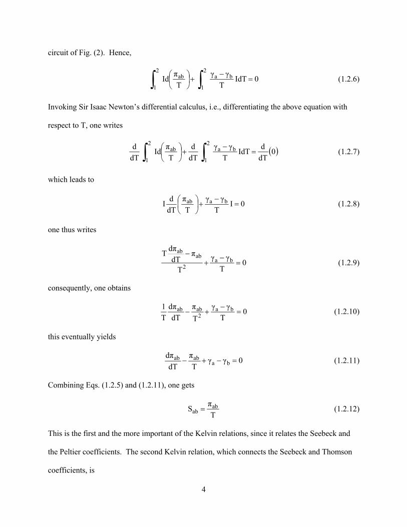
circuit of Fig. (2). Hence,
∫∫ =−
+⎟⎠⎞
⎜⎝⎛ 2
1
ba2
1
ab 0IdTTγγ
TπId (1.2.6)
Invoking Sir Isaac Newton’s differential calculus, i.e., differentiating the above equation with
respect to T, one writes
( )∫∫ =−
+⎟⎠⎞
⎜⎝⎛ 2
1
ba2
1
ab 0dTdIdT
Tγγ
dTd
TπId
dTd (1.2.7)
which leads to
0ITγγ
Tπ
dTdI baab =
−+⎟⎠⎞
⎜⎝⎛ (1.2.8)
one thus writes
0Tγγ
T
πdT
dπTba
2
abab
=−
+−
(1.2.9)
consequently, one obtains
0Tγγ
Tπ
dTdπ
T1 ba
2abab =
−+− (1.2.10)
this eventually yields
0γγTπ
dTdπ
baabab =−+− (1.2.11)
Combining Eqs. (1.2.5) and (1.2.11), one gets
TπS ab
ab = (1.2.12)
This is the first and the more important of the Kelvin relations, since it relates the Seebeck and
the Peltier coefficients. The second Kelvin relation, which connects the Seebeck and Thomson
coefficients, is
4

Tγγ
dTdS baab −
= (1.2.13)
Both of Kelvin’s laws have been confirmed, within experimental error, for a number of
thermocouple materials2. However, it has been reported that Eq. (1.2.12) is not strictly obeyed
for a germanium-copper couple3. In this case, it appears that the value of the Peltier coefficient,
π, is less than the product, ST. In spite of this fact, it seems that the Kelvin relations are
applicable to the materials used in thermoelectric applications, and their validity will be assumed
here.
The Seebeck and Peltier coefficients are both defined for junctions between two
conductors, but the Thomson coefficient is a property of a single conductor. Eq. (1.2.13)
suggests a way of defining the absolute Seebeck coefficient for a single material, namely by
putting
TdT
dS γ= (1.2.14)
It is established from the third law of thermodynamics that the Seebeck coefficient is zero, for all
junctions, at the absolute zero of temperature; the absolute Seebeck coefficient of any material is,
therefore, taken to be zero at this temperature. Thus,
∫ γ=
T
0dT
TS (1.2.15)
The absolute Seebeck coefficient of a material at very low temperatures may be
determined by joining it to a superconductor, the latter possessing zero thermoelectric
coefficients. This procedure has been carried out for pure lead up to 18K,4 and the Thomson
coefficient for lead has been measured between 20K and room temperature5. Its value in the
range between 18K and 20K can be accurately extrapolated. Thus, by use of Eq. (1.2.15), the
5

absolute Seebeck coefficient of lead has been established. The absolute Seebeck coefficient of
any other conductor may be determined by joining it to lead.
1.3 Theory of Thermoelectric Devices
In spite of the fact that thermoelectric effects have been known for a long time,
practically the only devices based upon them, which have been employed until recently, are
thermocouples for the measurement of temperature, and thermopiles for the detection of radiant
energy. Both applications utilize the Seebeck effect; in fact, they involve the thermoelectric
generation of electricity from heat. In the past this process has been extremely inefficient, but
the high sensitivity of the associated instruments has enabled such devices to be employed
satisfactorily. However, even inefficient thermoelectric refrigeration has been impossible up to
the last several years.
The basic theory of thermoelectric generators and refrigerators was first derived
satisfactorily by Altenkirch in 19096 and 19117. He showed that, for both applications, materials
were required with high thermoelectric coefficients, high electrical conductivities to minimize
Joule heating, and low thermal conductivities, to reduce heat transfer losses. However, it was
quite a different matter, knowing the favorable properties, and obtaining materials embodying
them, and so long as metallic thermocouples were employed, no real progress was made. It is
only since semiconductor thermocouples have been prepared that reasonably efficient
thermoelectric generators and refrigerators have become possible.
1.4 Coefficient of Performance of a Thermoelectric Refrigerator
One of the virtues of thermoelectric generation and refrigeration is the fact that the
efficiency is independent of the capacity of the unit. The coefficient of performance of a
thermoelectric refrigerator can, therefore, be derived on the basis of the single couple shown in
6
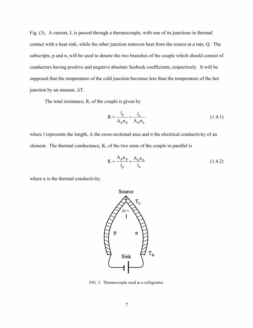
Fig. (3). A current, I, is passed through a thermocouple, with one of its junctions in thermal
contact with a heat sink, while the other junction removes heat from the source at a rate, Q. The
subscripts, p and n, will be used to denote the two branches of the couple which should consist of
conductors having positive and negative absolute Seebeck coefficients, respectively. It will be
supposed that the temperature of the cold junction becomes less than the temperature of the hot
junction by an amount, ΔT.
The total resistance, R, of the couple is given by
nn
n
pp
p
σAσAR ll
+= (1.4.1)
where l represents the length, A the cross-sectional area and σ the electrical conductivity of an
element. The thermal conductance, K, of the two arms of the couple in parallel is
n
nn
p
pp κAκAK
ll+= (1.4.2)
where κ is the thermal conductivity.
TH
TC
Source
I
np
Sink TH
TC
Source
I
np
Sink
FIG. 3. Thermocouple used as a refrigerator.
7

As a result of the Peltier effect, there is a rate of cooling Q=πpnI at the cold junction.
From Kelvin’s first relation, this becomes
TISIQ pnpn =π=
where T is the absolute temperature at which the cooling, or the heat transfer, rate Q, from the
source to the cold junction, occurs. Let us investigate this a little further by doing the following
transformation
CCHCH
M T2
TT2
TT2TTT =
−−
+=
Δ−= (1.4.3)
The above proves that the cooling rate, Q, may be calculated from the temperature TC, which is
that of the cold junction. One may thus write
I2TTSITSITSIQ MpnCpnpnpn ⎟⎠⎞
⎜⎝⎛ Δ
−===π= (1.4.4)
where TM is the mean absolute temperature of the hot and cold junctions. The cooling effect is
opposed by Joule heating in the branches, and by heat conducted from the hot junctions. It may
be shown that half of the overall Joule heating finds its way to each junction. Thus the rate of
absorption of heat from the source is
TKRI21I
2TTSQ 2
Mpna Δ−−⎟⎠⎞
⎜⎝⎛ Δ
−= (1.4.5)
While writing the above equation, the Thomson effect has been neglected.
Part of the potential difference applied to the couple is employed in overcoming the
resistance of the branches, and part is used to balance the Seebeck voltage, resulting from the
temperature difference between the junctions. One thus writes
IRTSV pn +Δ=Δ (1.4.6)
Thus, the power, W, supplied to the couple is given by
8
(1.4.7) RITISVIW 2pn +Δ=Δ=
The coefficient of performance for refrigeration, Φ, is defined as the ratio, Qa/W. Hence,
( )
RITIS
TKRI21I2/TTS
WQ
2pn
2Mpn
a
+Δ
Δ−−Δ−==Φ (1.4.8)
For a given pair of thermoelectric materials, and for given hot and cold junction
temperatures, the coefficient of performance is a function of the current, I, and also of the
resistance, R, and the thermal conductance, K. However, the latter two quantities are not
independent, and only a single relation between the dimensions of the elements is really
involved. For a specified cooling capacity, the ratio of length to cross-sectional area for an
element should rise with the electrical and thermal conductivities. A balance is then struck
between the effects of resistance heating and thermal conductance. It may be shown7 that Φ
reaches a maximum value when the dimensions of the elements obey the rule
2/1
nn
pp
pn
np
AA
⎟⎟⎠
⎞⎜⎜⎝
⎛κσ
κσ=
ll
(1.4.9)
Consequently,
22/1
n
n2/1
p
pKR⎪⎭
⎪⎬⎫
⎪⎩
⎪⎨⎧
⎟⎟⎠
⎞⎜⎜⎝
⎛σκ
+⎟⎟⎠
⎞⎜⎜⎝
⎛
σ
κ= (1.4.10)
and
( )( ) ( ) ( ) ( ){ }
( ) ( )2pn
22/1nn
2/1pp
2Mpn
IRIRTS
//TIR21IR2/TTS
+Δ
σκ+σκΔ−−Δ−=Φ (1.4.11)
By differentiation of Φ with respect to the product IR, the optimum current for a specific
temperature difference may be found. It is given by
9

( )1ZT1
TSIR
M
pnopt −+
Δ= (1.4.12)
where
22/1
n
n2/1
p
p
2npS
Z
⎪⎭
⎪⎬⎫
⎪⎩
⎪⎨⎧
⎟⎟⎠
⎞⎜⎜⎝
⎛σκ
+⎟⎟⎠
⎞⎜⎜⎝
⎛
σ
κ= (1.4.13)
Substituting the optimum value of IR in Eq. (1.4.11), it is found that the maximum
coefficient of performance is given by
( )( ) 2
11ZT1T1ZT1T
M
MMmax −
++Δ
−+=Φ (1.4.14)
Clearly, when the values of TM and ΔT are given, the coefficient of performance rises with
increase of Z. Z is, therefore, a figure of merit for the thermocouple.
It may be noted that as Z tends towards infinity, the value of Φ, given by Eq. (1.4.14),
approaches the value
T
TT
2/TT21
TT
lim CMMmax
Z Δ=
ΔΔ−
=−Δ
=Φ=Φ∞→
(1.4.15)
As expected, this is the coefficient of performance of an ideal thermodynamic refrigerating
machine or an inverted Carnot engine.
A thermoelectric heat pump operates exactly the same way as a thermoelectric
refrigerator, with the only difference that the desired effect, or result, is the heating rate that is
produced at the hot junction, and transferred to the sink, which could be a certain environment,
or enclosure. Thus, for a thermoelectric heat pump, the coefficient of performance is
Φ+=+=+
=Ψ 1WQ1
WQW (1.4.16)
10

where Φ is the coefficient of performance for refrigeration.
1.5 The Figure of Merit Z
The question arises as to the values of the parameters which should be used in calculating
the figure of merit, Z, if ΔT is large, since S, σ and κ are all temperature dependent. Since the
Joule heating and thermal conduction effects involve the whole of the couple, it is apparent that
mean values of σ and κ are required. However, since the Peltier effect is localized, it might be
thought that the value of S at the cold junction should be employed. This conclusion is found to
be false, when the Thomson effect is taken into account8.
The Thomson cooling in the whole of an element amounts to ∫ γdTI which, from
Kelvin’s second relation, is equal to ∫TdSI . Half of this cooling appears at each junction.
Thus, instead of the Peltier cooling SCTCI, we should use an overall rate of cooling
∫+H
CCC TdSI
21ITS , where the subscripts, C and H, refer to the cold and hot junctions,
respectively. Now, the Thomson term, in the expression for the overall cooling, is only a small
faction of the Peltier term. It is, therefore, a reasonable approximation to put
(1.5.1) ( CCH
H
CC
H
CTSSdSTTdS −== ∫∫ )
It is then found that
IT2
SSTdSI
21ITS C
CHH
CCC ⎟
⎠⎞
⎜⎝⎛ +
=+ ∫ (1.5.2)
Thus, the Thomson effect can be taken into account, if the mean value of the Seebeck
coefficient, S, rather than the value at the cold junction, is used. The figure of merit, Z, thus
11
involves the mean values of all the parameters.
In comparing different thermoelectric materials, it is rather inconvenient to deal with the
figure of merit, Z, as defined by Eq. (1.4.13). We, therefore, define a figure of merit, Z, for a
single material as
κσ
= 2SZ (1.5.3)
The figure of merit, Z, of a thermoelectric device is strictly equal to the mean of the values of Z
for the two elements, Zp and Zn, respectively, only in exceptional circumstances. In general, Z
must be regarded as a rather complicated average of Zp and Zn. The use of an individual figure
of merit, as defined by Eq. (1.5.3), is justified by the fact that nowadays the values of Zp and Zn
are never very much different in the thermocouples which are most suitable for thermoelectric
applications.
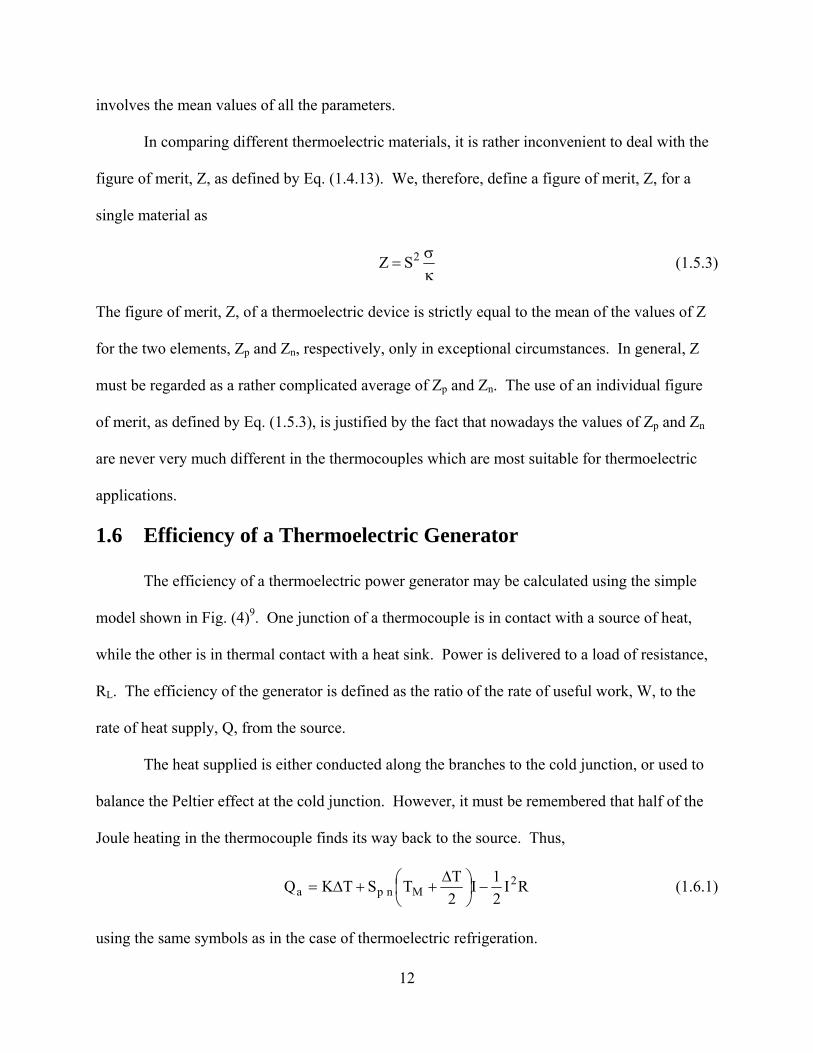
1.6 Efficiency of a Thermoelectric Generator
The efficiency of a thermoelectric power generator may be calculated using the simple
model shown in Fig. (4)9. One junction of a thermocouple is in contact with a source of heat,
while the other is in thermal contact with a heat sink. Power is delivered to a load of resistance,
RL. The efficiency of the generator is defined as the ratio of the rate of useful work, W, to the
rate of heat supply, Q, from the source.
The heat supplied is either conducted along the branches to the cold junction, or used to
balance the Peltier effect at the cold junction. However, it must be remembered that half of the
Joule heating in the thermocouple finds its way back to the source. Thus,
RI21I
2TTSTKQ 2
Mnpa −⎟⎠⎞
⎜⎝⎛ Δ
++Δ= (1.6.1)
using the same symbols as in the case of thermoelectric refrigeration.
12
For maximum power output from a given couple, the load resistance, RL, should be made
equal to the generator resistance, R. The useful work is then
( )R4
TSW
22np Δ
= (1.6.2)
since half of the thermoelectric voltage, SpnΔT, appears across the load.
The efficiency, η, is given by
2np
MSRK4
2TT2
T
+Δ
+
Δ=η (1.6.3)
The dimensions of the thermoelements or branches should obey Eq. (1.4.9), therefore
Z4
2TT2
T
M +Δ
+
Δ=η (1.6.4)
Since the efficiency rises with Z, this quantity is a figure of merit for thermoelectric generation
as well as for refrigeration.
If Z tends to infinity, η, as given by Eq. (1.6.4), approaches the value
2TT2
T
MΔ
+
Δ=η (1.6.5)
which is only about half the efficiency of an ideal thermodynamic machine, or heat engine. The
reason is that, when the maximum efficiency is required, RL should not be made equal to R. It
may be shown that the maximum efficiency is obtained when
( 2/1M
L ZT1 )R
Rr +== (1.6.6)
Therefore,
13
( )( ) 2
TT1r1r
T
M
max Δ+
−+
Δ=η (1.6.7)
Source
np
Sink
RL
Source
np
Sink
RL
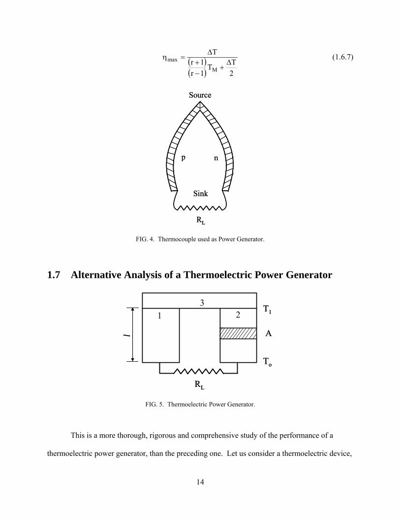
FIG. 4. Thermocouple used as Power Generator.
1.7 Alternative Analysis of a Thermoelectric Power Generator
RL
321
A
T1
To
l
RL
321
A
T1
To
l
FIG. 5. Thermoelectric Power Generator.
This is a more thorough, rigorous and comprehensive study of the performance of a
thermoelectric power generator, than the preceding one. Let us consider a thermoelectric device,
14

Fig. (5), consisting of a p-type thermoelement or branch, (1), and an n-type thermoelement or
branch, (2); joined by a metallic bridge, (3), which constitutes the hot junction. An external
resistance, RL, is connected in circuit across the cold ends of the thermoelements. This
resistance acts as a load for the electrical energy generated; it thus constitutes the cold junction of
the device. When the potential difference across the cold ends of the circuit, without the load, is
denoted by U volts, the power delivered by the thermoelements, or device, will be
L
2
RUW = (1.7.1)
whilst the current
LR
UI = (1.7.2)
Obviously, both thermoelements, (1) and (2), normally comprise either the same, or different,
semiconducting materials. This is deliberately done in order to maximize the figure of merit and
the performance of thermoelectric devices.
We shall denote the thermal emf, which is, in this case, equal to the sum of the thermal
emf’s of the two branches, by SVK-1. Thus,
21np21np12pn SSSSSSSSSSS +=+=−=−=== (1.7.3)
The hot ends, joined by the bridge, are maintained at a temperature, T1, receiving heat
energy from a source with a slightly higher temperature. The cold ends are at a temperature, To,
slightly above the temperature of the surroundings, or of the heat exchange medium.
We shall denote the internal resistances of the two branches by R1 and R2, and their
thermal conductances by K1 and K2. Denoting the electrical resistivities by ρ, the thermal
conductivities by κ, and assuming that the lengths of both thermoelements, or rods, are equal to l,
and their cross-sectional areas are A1 and A2, we have
15

l⎟⎟⎠
⎞⎜⎜⎝
⎛ ρ+
ρ=+=
2
2
1
121 AA
RRR (1.7.4)
( )l1AAKKK 221121 κ+κ=+= (1.7.5)
On the basis of the general laws of thermoelectric phenomena, we can calculate the
Peltier heat generated and absorbed by the thermoelements, considered together as one entity
constituting the device, at its two ends or junctions, the Thomson heat generated or absorbed
inside the thermoelements or rods, the heat transferred by conduction from the hot to the cold
ends, the Joule heat generated by the current in the rods or thermoelements, and the useful
electrical energy delivered by the thermoelements.
The amount of heat energy, QT1, received by the hot junctions of both thermoelements,
due to the Peltier effect, is
11T1T TISQ = (1.7.6)
The power, QTo, delivered at the cold junction is
oTT TISQOO
−= (1.7.7)
The Thomson heat, QTh, generated in each rod or thermoelement is, according to Eq.
(1.2.13),
IdTdTdSTQ
1T
OTTh ∫±= (1.7.8)
In the special case, when S at both ends has the same value, QTh = 0.
The heat flux, Qh, transferred from the hot junction to the cold junction through the two
thermoelements is
( )o1h TTKQ −= (1.7.9)
16

The Joule heat generated in the two thermoelements, branches or rods is
(1.7.10) RIQ 2J =
The useful power, W, delivered by the two thermoelements, or device, is
(1.7.11) L2RIW =
The current is
( )
RRTTS
IL
o1+−
= (1.7.12)
Setting
mR
R L = (1.7.13)
we have
( ) ( )1mR1TTTSQ o11
2
1TT1 +−= (1.7.14)
( )( )2
2o1
2
1mRmTTSW+
−= (1.7.15)
For the time being, we shall neglect the Thomson heat, regarding it as small in
comparison with the other terms, and shall assume SSSOTT ==
1. When , the Thomson
heat is accounted for, in the determination of the efficiency, by substituting for S the mean value
for the two ends
OTT SS ≠1
2
SSS
OT1T += (1.7.16)
Of the total Joule heat, I2R, generated in the thermoelements, half passes to the hot
junction, returning the power
17

RI21Q
21 2
J = (1.7.17)
and the rest is transferred to the cold junction.
The efficiency, η, will be defined as the ratio of the useful electrical energy, I2RL,
delivered to the external circuit, to the energy consumed, or received, from the heat source. The
latter consists of the Peltier heat, , and the heat, Qh, transferred by conduction to the cold
junction, from which it is necessary to deduct the electrical energy,
1TQ
21 I2R, returned to the heat
source.
( )
( )
( ) ( ) ( ) ( )( )
=
+
−−−+
+−
+−
=−+
=η
2
2o1
2
o1o112
22
o12
2h1T
1mRTTS
21TTK
1m1
R1TTTS
1mm
R1TTS
RI21QQ
W
( )1m
1T
TT21
T1m
SKR1
1mm
TTT
1
o1
12
1
o1
+−
−+
+
+−= (1.7.18)
Thus, the efficiency of the thermoelements, or thermoelectric device, is fully determined
by: a) The hot and cold junction temperatures. b) The quantity, 2SKR , which depends on the
properties of the materials, used in the manufacture of the thermoelements, and which will be
denoted by, Z-1, so that
KRSZ
2= (1.7.19)
and, finally,
c) The selected ratio, R
Rm L= (1.7.20)
18

In order to achieve an efficiency as high as possible in thermoelements, or devices, at
given values of S, κ and ρ, and an arbitrary ratio, m, as given by Eq. (1.61), it is necessary to find
the optimum cross-sectional areas, A1 and A2, so that at given values of κ and ρ, the product, KR,
is minimum. To find the condition for a minimum of KR, we shall differentiate
( )1
212
2
1212211
2
2
1
12211 A
AAA
AAAAKR ρκ+ρκ+ρκ+ρκ=⎟
⎟⎠
⎞⎜⎜⎝
⎛ ρ+
ρκ+κ=
with respect to A1/A2 and equate the derivative to zero. This gives
2
2
1
2
2
1
1
AA
⎟⎟⎠
⎞⎜⎜⎝
⎛=
ρκ
κ
ρ (1.7.21)
At this value of A1/A2
( )22211KR ρκ+ρκ= (1.7.22)
( )22211
22 SKRSZ
ρκ+ρκ== (1.7.23)
This expression contains only the properties of the materials constituting the two
branches or thermoelements of the device, but not their dimensions.
We now need to find the ratio, m = RL / R, which gives the highest efficiency. The
condition for delivering the maximum power to the load leads, in the case of a thermoelectric
device, as with other current sources, to the requirement: m = 1, which when substituted into Eq.
(1.7.18) yields
( )o11
o1
TT41
Z2T
TT21
−−+
−=η (1.7.24)
We shall find the condition for the maximum efficiency by differentiating Eq. (1.7.18) with
respect to m, and setting
19

0m
=∂η∂ (1.7.25)
which yields
( )o1opt
L TTZ211M
RR
++==⎟⎠⎞
⎜⎝⎛ (1.7.26)
where M is a dimensionless number.
Substituting this optimum value of m, denoted here by M, into Eq. (1.7.18), we get
1
o1
o1
TT
M
1MT
TT
+
−−=η (1.7.27)
Henceforth, η will only refer to this maximum efficiency. The first factor in Eq. (1.7.27)
represents the thermodynamic efficiency of a reversible heat, or Carnot, engine, and the second
describes the reduction in the efficiency due to losses, brought about by irreversibility, resulting
from heat conduction (κ) and Joule heat (ρ), entering into the expression for Z.
The greater is M, in comparison with unity, i.e., the larger the values of Z and T1+To, the
smaller is the reduction in the efficiency due to losses brought about by irreversibility.
Therefore, an increase in the hot junction temperature, T1, increases η not only by increasing the
value of the efficiency of a reversible engine, 1
o1T
TT −, but also because of the simultaneous
increase in M, at a given Z.
This equation also clearly shows that, in order to achieve maximum efficiency, a material
has to satisfy only one condition, namely the maximum value of Z compatible with the
maximum temperature, T1, of the heat source, or, more precisely, the maximum product,
2TT
Z o1 + , attainable for the given material.
20

1.8 Early Developments
At the beginning of the past century, the theory of metals was based on the concept of the
presence in each metal of a certain concentration of free electrons, n, different for differing
metals, moving at random within the metal, in a manner similar to gas molecules. According to
these theories, as developed by Rieke, Drude, Lorentz and Debye, electrons were governed by
the same Boltzmann statistics as gaseous molecules. As in a gas, their average translational
energies were regarded as equal to kT23 , where k is the Boltzmann constant and T is the
absolute temperature. The thermal emf, V, in an open circuit, consisting of two metals,
calculated according to this theory, is
∫=2T
1T 1
2 dTnn
lnekV (1.8.1)
It can be readily calculated that S=86μVK-1 for 7.2/ 12 =nn , which is much higher than the
experimentally observed value of S, for cases where , since for the majority of
metals S does not exceed a few μVK-1. According to the quantum theory of metals developed by
Sommerfeld, who applied Fermi-Dirac statistics to electrons in metals, the thermal emf between
two metals is, to a first approximation, equal to zero. Only the next approximation leads to a
certain finite, although very small, value of S. All this is not surprising. Let us consider a
metallic rod, the ends of which are at different temperatures. Since the temperature does not
change the concentration of electrons, n, in the metal, but brings about only a slight redistribution
in their thermal agitation velocities, it is obvious that a large thermal emf cannot arise in such a
metal. The state of semiconductors in the quantum theory is similar to that of the classical metal,
considered at the beginning of the 20th century. Some of the current-carrying particles in
7.2/ 12 >nn
21

semiconductors may be considered to be “free.” The concentration of free electrons in
semiconductors varies, but is usually so much smaller than in metals, that the Boltzmann
classical statistics are often applicable. A rise in temperature in certain regions leads to a change
in both the concentration of free electrons and their kinetic energy, which, as in the case of gas
molecules, may be equated to kT23 . Let us consider a rod of semiconductor in which there is a
temperature gradient, dT/dx. At the hot end of the rod, both the concentration and the velocities
of the electrons are higher than at the cold end. Therefore, more electrons will start to diffuse in
the direction of the temperature gradient, than in the opposite direction. The diffusion flux,
carrying the negative charge away from the hot end, and transferring it to the cold end, sets up a
potential difference between the ends. The diffusion process is increasingly retarded by the
electrical field in the interior of the semiconductor, until the flux of electrons, caused by
diffusion, is equal to the reverse flux, caused by the potential difference which has arisen. Under
these conditions, a dynamic electron equilibrium in the semiconductor will be established, under
which the temperature difference between the ends of the rods will maintain a corresponding
potential difference.
The number of electrons passing through any cross-section of the conductor, in unit time,
in both directions, are equal. However, the velocities of electrons proceeding from the hot end
are higher than the velocities of electrons passing through the given cross-section from the cold
end. This difference ensures that there is a continuous transfer of heat energy in the direction of
the temperature gradient, without any actual charge transfer.
The heat transfer mechanism is substantially different when negative and positive charge
carriers participate simultaneously in the current. Simultaneous transfer of equal numbers of
holes and electrons does now lead to an accumulation of the charge and an increase in the
22

potential. Simultaneous diffusion of electrons and holes, from the hot end to the cold end, is
caused not only by the difference in the carrier velocities, but also by their concentration
gradient.
In the case of such a bipolar diffusion a thermal emf can also arise due to the following
two factors: 1) When the concentration of one type of carrier exceeds the concentration of the
opposite type of carrier, the flux of the first type of carrier will carry, towards the cold end,
predominantly a charge which will retard their motion and, conversely, accelerate the carriers of
the opposite sign, until the fluxes of both carriers are equal. An electric field, governed by the
temperature gradient, will thus be established. 2) The difference of charge carrier mobilities
forms the second source of thermal emfs. The mobility, μ, is related to the diffusion coefficient,
D, by the universal relationship, established by Einstein:
kTe
D=
μ (1.8.2)
Under the effect of the concentration gradient, set up by the temperature gradient, the
carriers, characterized by higher values of μ and D, would have moved forward, had they not
created a space charge on becoming separated from the carriers of opposite sign. The
corresponding electric field, E, retards their motion, and accelerates the slower carriers of the
opposite sign. The electric field, E, equalizes the velocities of both types of carrier, enabling
them to diffuse as a single body.
Therefore, even when thermal agitation creates an equal number of current carriers of
each sign, their diffusion produces an electric field in the conductor, depending on the difference
in carrier mobilities. The expression for this electric field, E, will be similar to that for the
diffusion of ions in an electrolyte, namely
23

21
21oEE
μ+μ
μ−μ= (1.8.3)
where Eo is the electric field which would have existed in the presence of current carriers of one
sign only, and μ1 and μ2 are the mobilities of positive and negative charges.
The advantage of semiconductors, when used as materials for thermoelements, is due to
their higher values of thermal emf. In metals, the concentration of free charge carriers is high, of
the order of 1022 carriers cm-3, and does not depend much on temperature. The kinetic energy of
the highly degenerate electrons is virtually independent of temperature, and the same applies to
the contact potential of the metal at its boundaries. Under such conditions, thermal emfs, as a
rule, do not exceed a few μVK-1. In semiconductors, however, temperature may have a
pronounced effect on the concentration, n, and kinetic energy, E, of free charge carriers, while
the absolute value of the concentration is smaller by a few orders of magnitude, namely 1014 to
1020 carriers cm-3. The contact potential, Φ, of semiconductors with respect to metals, and the
corresponding chemical potential, μ, are also functions of temperature. Thermal emfs amount in
this case to hundreds μVK-1.
The thermal emf per degree Kelvin, S, may be regarded as an entropy flux of 1 Coulomb
of electrical charge. The value of S depends not only on the entropy difference between two
substances, but also on the conditions of the motion of the electrons. These conditions may, in
turn, depend on the nature of the semiconductor, and on the mechanism of electron scattering in
the transfer of electrons from one portion of the semiconductor to another. Therefore, the value
of S is closely related to the mobility, μ, which is governed by the same scattering mechanism.
1.9 Materials for Semiconductor Thermoelements
Let us now consider the selection of the most suitable materials for thermoelements.
24

First of all, it should be noted that semiconductors, owing to their much higher values of S, are
definitely preferable to metals. The higher the value of Z = S2/κρ, for the individual branches of
the thermoelement, the higher is the value of ( ) ( )222112
21 /SSZ ρκ+ρκ+= , which
determines the efficiency of the entire thermoelement or device. The ratio of thermal
conductivity to electrical conductivity, for all metals, is close to the theoretical value predicted
by quantum mechanics: κ/σ = (π2/3) (k/e)2 T = 2.44 x10⁻⁸ T. The thermal conductivity of a
semiconductor, κ, is composed of the electronic thermal conductivity, κel, and the thermal
conductivity due to thermal vibrations and the propagation of heat waves, usually denoted as
phonon, or lattice, thermal conductivity: κ = κel + κph. The former is related to the electrical
conductivity by the Wiedemann-Franz law. However, the coefficient of proportionality has a
value equal to that for metals, κel / σ = (π2/3) (k/e)2 T, only at very high concentrations of free
electrons, namely more than 2.5x10¹⁹ carriers cm-3, when the latter must be regarded as
degenerate. At lower concentrations, usually prevailing in semiconductors, κel / σ = 2 (k/e)2 T =
1.48 x10⁻⁸ TV2K-1. In general, the Wiedemann-Franz law for semiconductors has the following
form: κel / σ = (r+2) (k/e)2 T, which for atomic lattices with r = 0, reduces to the preceding
equation, where r is the electronic scattering parameter or constant that appears in the formula
giving the electron mean free path length, l , as a function of the kinetic energy, namely . rE∝l
By analogy with diffusion and thermal conduction in gases, the phonon part of thermal
conductivity, κph, can be expressed as λ=κ vc31 , where c is the specific heat, v is the sound
velocity and λ is the phonon mean free path length. The value of the thermal conductivity, κph,
of a semiconductor is also related to electron mobility, μ, and therefore also to electrical
conductivity. Both phonons and electrons are scattered by the same inhomogeneities of the
25

crystalline lattice, but the degree of scattering is different, owing to their different wavelengths:
7x10⁻⁷cm for electrons and approximately 5x10⁻⁸cm for phonons, and their different physical
nature.
There should exist some correlation between λ and the mean free path length of
electrons, l . As pointed out by H.J. Goldsmid, the ratio, μ / κph, governing the value of Z of
thermocouples, increases with increasing atomic weight. The factors affecting the value of the
phonon thermal conductivity, κph, are as follows: κph decreases not only with increasing average
atomic weight, but also in going over from purely valence type to ionic compounds, i.e., from
elements in group IV of the periodic system towards compounds of groups III with V, II with IV
and I with VII.
In order to obtain the highest values of (S2σ)max, it is desirable to select semiconductors
with maximum mobility, μ, and minimum effective mass, m*. The phonon thermal conductivity
is strongly affected by scattering. It decreases with increase of the atomic mass and with the
reduction of the hardness of the material. For ionic compounds, κph has a lower value than for
covalent compounds. When excess, or impurity, atoms become ionized in the lattice, giving up
their electrons to be free, they produce electronic conductivity; on the other hand, when impurity
atoms pick up electrons from the band filled with valence electrons, hole conductivity is
produced.
The following are A. F. Ioffe’s qualitative criteria for minimizing the lattice thermal
conductivity: 1) The thermal conductivity would be expected to be minimum in crystals,
consisting of heavy atoms or ions, with a low Young’s modulus. 2) The minimum thermal
conductivity can be expected to occur in crystals with a large thermal expansion coefficient. 3)
In nondegenerate semiconductors, the wavelength of electronic waves, at room temperature, λel,
26

is tens of times larger than the interatomic distance ( ), whereas most of the normal
lattice vibrations occur at a wavelength, λph, which is of the order of the lattice constant
( ). This difference between λel and λph makes it possible to create
inhomogeneities in the crystal lattice, which are effective in scattering phonons, but which
virtually do not scatter electron waves, i.e., do not reduce the carrier mobility. Such
inhomogeneities can, in particular, be produced by the introduction into the lattice of neutral
impurity atoms, or by the formation of solid solutions, based on chemical compounds
crystallizing in similar lattices.
cm10 6el
−≈λ
cm10 8ph
−≈λ
The lattice thermal conductivity, κph, depends on the phonon scattering mechanism. At
temperatures above the Debye temperature: 1) in ideal crystals, i.e., for the scattering
of phonons by phonons. 2) κph is independent of temperature for the scattering of phonons by
lattice defects. Intermediate cases may, of course, also occur, with both scattering mechanisms
participating; in this case, the numbers of collisions of phonons with phonons, and with defects,
i.e., the reciprocals of the mean free path lengths, are additive. The temperature dependence of
the numerator, S2σ, in the expression for Z, is governed by the temperature dependence of the
carrier concentration and the mobility. It has been mentioned earlier that, for S2σ to preserve its
maximum value over a wide temperature range, the carrier concentration should rise gradually
with temperature: namely . However, there are no substances in nature which follow
such a law and, therefore, the materials for thermocouple arms consist, as a rule, of semimetals,
in which the carrier concentration is constant. Depending on the working temperature range, a
suitable number of donors or acceptors is introduced into the semimetal, so as to fulfill the
condition
1ph T−∝κ
2/3Tn ∝
27

( ) r
3
2/3
eh
kT*m22n
π= (1.9.1)
approximately, within this particular temperature range. Therefore, the temperature dependence
of S2σ in semimetals is entirely governed by the temperature dependence of the mobility.
28

Chapter 2
Minimizing Thermal Conductivity
2.1 Atomic Weight and Melting Point
First, one considers pure elements and compounds, and one directs attention to the so-
called high-temperature region, over which lattice thermal conductivity varies as T-1. This
region usually extends below room temperature and, for most materials of interest, even below
liquid nitrogen temperature. It may be assumed that phonon-phonon scattering is dominant
under the conditions stated.
Some success in predicting high-temperature lattice thermal conductivity was achieved
by Leibfried and Schlömann 8. By using a variational method, they found that
T
MVh
k5.3 2
3D
31
3B
Lγ
θ⎟⎠⎞
⎜⎝⎛=κ (2.1.1)
where M is the average mass per atom, V is the average atomic volume and γ is the Grüneisen
parameter, which enters into the equation of state for solids and, together with the expansion
coefficient, is a measure of the anharmonicity of lattice vibrations.
One can obtain Leibfried and Schlömann’s formula, or rather one that differs from it only
in the value of the numerical constant, by the following simple means: One starts by using
Dugdale and MacDonald’s argument that there should be a relationship between κL and the
thermal expansion coefficient, αT, because both depend on the anharmonicity of interatomic
forces. Dugdale and MacDonald 19 showed that anharmonicity can be represented by the
dimensionless quantity, αTγT, and they suggested that the phonon free path length, lt, should be
29

approximately equal to the lattice constant, a, divided by this quantity. Thus, by substitution in
Eq. (A2.2.6)
T3
ac
T
VL γα=κ
v (2.1.2)
One may eliminate αT from this equation by using the Debye equation of state
3
cVT
γχ=α (2.1.3)
where χ is the compressibility. The speed of sound, v, and χ are also related to the Debye
temperature, θD, through the equation
( )h
ak2 DB21
dθ
=χρ= −v (2.1.4)
where ρd is the density. Then, if a is set equal to the cube root of the atomic volume,
T
VMh
k8 2
3D
31
3B
Lγ
θ⎟⎠⎞
⎜⎝⎛=κ (2.1.5)
which may be compared with Eq. (2.1.1). Because one is not concerned with the value of the
numerical constant here, one may use either Eq. (2.1.1) or (2.1.5), and we opt for the latter.
Neither Eq. (2.1.2) nor (2.1.5) is as useful as one might hope in predicting the value of κL.
One of the relationships requires a knowledge of the expansion coefficient and the speed of
sound, whereas the other involves θD. Keyes20 showed that a more useful formula could be
obtained by using further approximations. His starting point was Lawson’s21 equation for
thermal conductivity,
2/1d
2/32LT3
aρχγ
=κ (2.1.6)
which is easily obtained from Eq. (2.1.2) or (2.1.5) by substitution of Eq. (2.1.4). Keyes then
30

eliminated the compressibility by use of the Lindemann melting rule,
m
mRT
Vε=χ (2.1.7)
where R is the gas constant and Tm is the melting temperature. This rule is based on the
assumption that a solid melts when the amplitude of the lattice vibrations reaches a fraction, εm,
of the lattice constant, εm being approximately the same for all substances. Keyes found that
67
32
d23
mL
A
TBT
ρ≅κ (2.1.8)
where
31
A3m
2
23
N3
RBεγ
= (2.1.9)
with NA being Avogadro’s number and A being the mean atomic weight. The factor, B, involves
only the universal constants, R and NA, and two quantities, γ and εm, that are unlikely to change
by much from one material to another. The variables, Tm, ρd and A, that appear in Eq. (2.1.8) for
thermal conductivity are, of course, known as soon as a material is first synthesized, so that, if
the equation is valid, it is a most useful aid for predicting κL.
By collecting data for a wide variety of dielectric crystals, Keyes was able to show that
Eq. (2.1.8) is always satisfied to within an order of magnitude, if B is set equal to 3x10⁻⁴ SI units.
If one selects different values of B for covalent and ionic crystals, much better agreement is
obtained. Thus, one may use B equal to 1.3x10⁻³ SI units for covalent materials, and 1.5x10⁻⁴ SI
units for ionic materials. Goldsmid72 has found good agreement between the predictions of the
Keyes rule, Eq. (2.1.8), and the experimental data for a variety of semiconductors, using a value
of 6x10⁻⁴ SI units for B.
31

It should be noted that elements or compounds of high mean atomic weight tend to have
low melting temperatures. Their densities are also usually high, but one expects that ρd2/3A-7/6
should decrease as the atomic weight rises. Thus, the Keyes rule supports the prediction of
Goldsmid and Douglas22 that materials of high mean atomic weight should have a low thermal
conductivity and should be chosen for thermoelectric applications.
Ioffe and Ioffe23 also drew attention to the dependence of thermal conductivity on atomic
weight, and demonstrated a difference between covalent and ionic crystals that is consistent with
the different values of B that are preferred for the respective types of material. One should avoid
inferring that ionic materials are likely to be better than covalent semiconductors in
thermoelectric energy conversion, on account of their lower range of thermal conductivity. Ionic
compounds invariably have very much smaller carrier mobilities, and the factor, μ(m*)3/2/κL,
appears to be highest for semiconductors in which covalent bonding is predominant.
2.2 Semiconductor Solid Solutions
Ioffe et al24 first made the interesting and useful suggestion that solid solutions or alloys might be
superior to elements or compounds in their thermoelectric properties. It was argued that, in
forming a solid solution between isomorphous crystals, the long-range order would be preserved,
so that the charge carriers, with their comparatively long wavelengths, would not suffer a
reduction in their mobility. On the other hand, phonons that contribute most to the transport of
heat have a much shorter wavelength and would be effectively scattered by the short-range
disorder, thus reducing the thermal conductivity.
Shortly afterwards, Airapetyants et al25 proposed a refinement of the above principle.
They considered that electrons would be more strongly scattered by disturbances in the
electropositive sublattice of a compound, whereas holes would be more strongly scattered by
32

disturbances in the electronegative sublattice. On this basis, positive and negative thermoelectric
materials should be produced from solid solutions in which there is disorder only in the
electronegative and electropositive sublattices, respectively.
Although there is some experimental evidence to support these views, they cannot be
regarded as firmly established. Indeed, they would seem to imply that there should be strong
scattering of both electrons and holes in solid solutions between elemental semiconductors,
whereas, in fact, silicon-germanium alloys have proved most useful as high-temperature
thermoelectric materials26.
Whether or not account should be taken of the principle of Airapetyants et al, it is clear
that the reduction of the lattice thermal conductivity, in certain solid solutions of both elements
and compounds, outweighs any fall in the mobility of the appropriate charge carriers. Therefore,
it is important to consider the mechanism by which phonon scattering occurs in such materials.
According to the Rayleigh theory, the scattering cross-section, σ, for point defects can be
expressed as
2
d
d4L
6
9qc4
⎟⎟⎠
⎞⎜⎜⎝
⎛ρρΔ
+χχΔπ
=σ (2.2.1)
where c is the linear dimension of the defect, qL is the magnitude of the phonon wave vector, Δχ
is the local change of compressibility and Δρd is the local density change. The applicability of
Rayleigh scattering has been discussed by Klemens27. Strictly speaking, the dimensions of the
defect should be much smaller than the wavelength of the radiation. For higher frequency
phonons, however, this is not true, even if c is no larger than the interatomic spacing.
Nevertheless, the use of the Rayleigh formula can be justified, because the short-wavelength
phonons are so strongly scattered by point defects, that they contribute very little to thermal
conductivity. Most of the heat transport then arises from phonons for which the Rayleigh theory
33
is applicable. The same argument allows us to use the Debye model for lattice vibrations of
alloys with more confidence than would be the case for simple elements or compounds.
Although we might expect normal processes to have some influence on thermal
conductivity, even at high temperatures (see Appendix A2), we can obtain a good idea o
effect of alloy scattering by assuming that the umklapp processes are predominant, ko→0. Eq
(A2.3.16), therefore, becomes
f the
.
⎟⎟⎠
⎞⎜⎜⎝
⎛ωω
ωω
≡⎟⎟⎠
⎞⎜⎜⎝
⎛ωω
ωω
=κκL −
o
D
D
o
o
D1
D
o
oarctantan (2.2.2)
where ωo/ ωD is defined by Eq. (A2.3.18). Here, κL is the thermal conductivity of the solid
tivity
ade.
ts
nons are scattered by variations of both elasticity and
solution and κo is that of the so-called virtual or pure crystal; κo is the lattice thermal conduc
that the solid solution would possess if it were perfectly ordered, that is, if point-defect scattering
were absent. The value of κo can be obtained by linear interpolation between the observed
thermal conductivities of the components of the solid solution, if no better estimate can be m
Note that, for group IV elements, elastic constants vary inversely with the fourth power of the
lattice spacing; this enables estimating θD accurately for any particular alloy, and certainly assis
in predicting κo and the speed of sound, v.
Now, Eq. (2.2.1) shows that the pho
density. The density, or mass-fluctuation, effect is easier to determine theoretically and might, in
fact, predominate in the type of alloy in which we are interested. In this case, the parameter, A,
in Eq. (A2.3.18) is given by
( )∑ −π=
i2
2ii
3MM
MMxN2
Av
(2.2.3)
where xi is the concentration of unit cells of mass Mi, M is the average mass per unit cell and N
34

is the number of unit cells per unit volume.
The additional effect of scattering due to elasticity fluctuations, or strain scattering, is
l more difficult to predict. However, we can outline the approach. A foreign atom changes loca
compressibility, because it has bonds different from those of the host atoms, and also because it
does not fit properly into a lattice site, thus straining the crystal. Based on the elastic continuum
model, an impurity atom of width, Iδ ′ (in its own lattice) will distort the space it occupies from
one having a width, δ, in the host lattice to one of width, δI, where
( ) δδ−δ′
δδΔ
≡μ+
μ=
δδ−δ IiI
1(2.2.4)
and
( )( )Gv212
Gv1
P
IP++
=μ (2.2.5)
G and υP are the bulk modulus and Poisson’s ratio for the host crystal, respectively, and GI is the
bulk modulus of the impurity crystal. Klemens has shown that the value of A in Eq. (A2.3.18),
for strain scattering, is given by
∑ ⎟⎠⎞
⎜⎝⎛
δδΔ
γ−Δπ
=i
2iI
iS 4.6GGx
NA (2.2.6)
where ΔGI ≡ GI – G and γ is the Grüneisen parameter.
ttering and strain scattering can be judged
om ex
The relative importance of mass-fluctuation sca
fr perimental data compared to a solid curve, calculated from Eq. (2.2.2), where ωD/ ωo is
determined using only the mass-fluctuation parameter, AM, given by Eq. (2.2.3). It is seen that,
for several of the solid solution systems, the experimental data lie close to the theoretical curve.
However, there is considerable disagreement in other systems. It is noteworthy that, where such
disagreement occurs, the observed thermal conductivity is less than predicted theoretically on the
35

basis of mass-fluctuation scattering alone. Then, it is reasonable to suggest that the discrepancies
can be attributed to a significant strain scattering effect.28
Chapter 3
Electron Transport in a Zero Magnetic Field
3.1 Single Bands
on to derive general expressions for the thermogalvanomagenetic
oeffic
etween the
We are now in a positi
c ients. We shall restrict ourselves, however, to the case of zero magnetic field. It will also
be supposed that we are dealing with one type of carrier, electrons or holes, residing in a single
energy band of the parabolic form described by Eq. (A3.1.7). It is also assumed that although
the charge carriers interact with the phonons, they have no significant effect on the distribution
of the latter. In other words, phonons are regarded merely as scattering centers.
The Boltzmann equation for the steady state, which represents a balance b
effects of the fields and the scattering processes, yields
( ) ( ) ( ) ( )
rEfr
ker&rEfk
EfEf o r&r
∂∂
−∂τ
(3.1.1)
where f and fo are the perturbed and unperturbed distribution functions, respectively, and
∂−=
−
kr
and
rr are the wave vector and the position vector of the charge carriers. We must solve this
uation to obtain f-fo, in terms of the electric field and the temperature gradient. It will b
assumed that the conductor is isotropic and that the fields and flows are all in the direction o
x-axis.
I
eq e
f the
f |f-fo| << fo, one can replace f by fo on the right-hand side of Eq. (3.1.1). Then, bearing
in mind that the Fermi distribution will be dependent on displacement through both the electric
36

field and the temperature gradient, we may show that
( ) ( ) ( )
⎟⎠⎞
⎝ ∂∂ζ−
+∂ζ
∂τ xT
TE
xEe (3.1.2)
where u is the velocity of the carriers in the x-direction. It may be noted that this equation will
s,
nge of energy from E to E+dE is
the x-
0dE (3.1.3)
where henceforth the upper sign in such an equation refers to electrons and the lower sign to
ζ−=0
dEEgEfEuw (3.1.4)
since E-ζ represents the total energy transported by a carrier. It will be noted that the upper limit
e to replace f by f-
in the
⎜⎛ ∂∂
=− Ef
uEfEf oo
apply equally well for holes and electrons, provided that the carrier energy, E, and the Fermi
energy, ζ, are measured from the appropriate band edge and in the appropriate direction. Thu
electron energies are measured upwards from the bottom of the conduction band, and hole
energies downwards from the top of the valence band.
The number of carriers per unit volume in the ra
f(E)g(E)dE, with g(E) given by Eq. (A3.1.7). Since the carriers, with charge m e, move in
direction with a velocity, u, the electric current density is
( ) ( )∞
= EgEeufi m∫
holes. Similarly, the rate of flow of heat per unit cross-sectional area, w, is
( ) ( ) ( )∞
∫
to the integrals in Eqs. (3.1.3) and (3.1.4) suggests that the bands are infinitely wide, but, in
practice, the function, f(E), always falls to zero before E becomes very large.
Since there can be no flow of charge or heat when f=fo, it is appropriat
fo above two equations. Also, in any case of interest to us, the thermal velocity of the
carriers will always be very much greater than any drift velocity. Thence, we may set
37

*m3
E2u 2 = (3.1.5)
since u2 will be one third of the mean square velocity corresponding to the energy, E. By
inserting Eq. (3.1.5) into Eqs. (3.1.3) and (3.1.4), we find
( ) ( )dE
xT
TE
xEEf
EEg*m3
e2i o
0e ⎟
⎠⎞
⎜⎝⎛
∂∂ζ−
+∂ζ∂
∂∂
τ= ∫∞
m (3.1.6)
and
( ) ( )∫∞
⎟⎠⎞
⎜⎝⎛
∂∂ζ−
+∂ζ∂
∂∂
τ+ζ
±=0
o2e dE
xT
TE
xEEf
EEg*m3
2ie
w (3.1.7)
To find an expression for the electrical resistivity or conductivity, σ, we set the
temperature gradient, , equal to zero. Also the electric field is given by .
Thence
xT ∂∂ / ( ) 1/ −∂∂± exζ
( ) ( )∫∞
∂∂
τ−
==σ0
oe
2dE
EEf
EEg*m3
e2iE
(3.1.8)
Alternatively, if the electric current is zero, Eq. (3.1.6) shows that
( ) ( ) ( ) ( ) ( )0dE
EEf
EEEgxT
T1dE
EEf
EEgx 0
oe
0
oe =
∂∂
ζ−τ∂∂
+∂
∂τ
∂ζ∂ ∫∫
∞∞ (3.1.9)
This is the specified condition for the definition of both the Seebeck coefficient and the thermal
conductivity. The Seebeck coefficient is defined by
Te
1Tx
xe1
xTe
xxTe
xxTS
111
1
∂ζ∂
±=∂∂
∂ζ∂
±=⎟⎠⎞
⎜⎝⎛
∂∂
∂ζ∂
±=⎟⎠⎞
⎜⎝⎛∂∂
⎟⎠⎞
⎜⎝⎛∂ζ∂
±=⎟⎠⎞
⎜⎝⎛∂∂
=−−
−−
E (3.1.10)
Now, substituting Eq. (3.1.10) into Eq. (3.1.9), we arrive at the following, more specific,
definition of the thermoelectric power:
38

( ) ( )
( ) ( )⎥⎥⎥⎥⎥
⎦
⎤
⎢⎢⎢⎢⎢
⎣
⎡
∂∂
τ
∂∂
τ
−ζ±=
∫∫
∞
∞
0
oe
0
o2e
dEEEf
EEg
dEEEf
EEg
eT1S (3.1.11)
It turns out that the Seebeck coefficient is always negative if the carriers are electrons, and
positive if the carriers are holes.
The electronic thermal conductivity is given by ( ) 1/ −∂∂− xTw and is found from Eqs.
(3.1.7) and (3.1.9). Thence
( ) ( )
( ) ( )( ) ( )
⎥⎥⎥⎥⎥
⎦
⎤
⎢⎢⎢⎢⎢
⎣
⎡
∂∂
τ−
∂∂
τ
∂∂
τ
=κ ∫∫∫ ∞
∞
∞
0
o3e
0
oe
0
o2e
e dEEEf
EEgdE
EEf
EEg
dEEEf
EEg
T*m32 (3.1.12)
The Peltier coefficient, П, can be found either from the Kelvin relation: , in terms
of the Seebeck coefficient, S, or as the ratio, w/i, when
ST=Π
0/ =∂∂ xT . The same value, of course,
results from each derivation.
The integrals that are found in Eqs. (3.1.8), (3.1.11) and (3.1.12) have the same general
form. They may be expressed conveniently as
( ) ( ) ( ) ( )∫∫∞ ++∞
+
∂∂
τ⎟⎠⎞
⎜⎝⎛π−=
∂∂
τ−=0
o23rs
o212
3
20
o1seS dE
EEf
ET*mh2
38dE
EEf
EEg*m3
T2K
(3.1.13)
where g and τe have been eliminated in terms of m*, r and τo, using Eqs. (A3.1.7) and (A3.2.2).
On integrating by parts, one finds that
( ) ( )∫∫
∞ ++∞ ++⎟⎠⎞
⎜⎝⎛ ++−=
∂∂
0o
21rs
0
o23rs
dEEfE23rsdE
EEf
E (3.1.14)
39

Thence we may write
( ) ( )21rs
23rs
Bo212
3
2S FTk23rsT*m
h2
38K
++
⎟⎠⎞
⎜⎝⎛ ++⎟
⎠⎞
⎜⎝⎛ ++τ⎟
⎠⎞
⎜⎝⎛π= (3.1.15)
where
(3.1.16) ( ) ( )∫∞
ξξξ=ξ0
on
n dfF
and use is made of the reduced energy, ξ, equal to , as a variable. Tk/E B
The expressions for the transport coefficients in terms of the integrals, KS, are
o
2K
Te
=σ (3.1.17)
⎟⎟⎠
⎞⎜⎜⎝
⎛−ζ±=
o
1KK
eT1S (3.1.18)
and
⎟⎟⎠
⎞⎜⎜⎝
⎛−=κ
o
21
22e KK
KT1 (3.1.19)
It is these equations that allow expressing the figure of merit, Z, in terms of ζ, m*, the relaxation
time parameters, τo and r, and κL. The lattice conductivity is involved because the total thermal
conductivity, κ, is given by
eL κ+κ=κ (3.1.20)
3.2 Degenerate and Nondegenerate Conductors
In general, it is necessary to use numerical methods to determine the transport properties
from Eqs. (3.1.17) to (3.1.20). However, if the Fermi energy is either much greater than or much
less than zero, it is possible to use simple approximations to the Fermi distribution function.
40

First, we shall consider the nondegenerate approximation that is applicable when
0Tk/ B <<ζ , that is, the Fermi level lies within the forbidden gap, well away from the
appropriate band edge. The approximation is very good when Tk4 B−<ζ , and is acceptable for
many purposes when Tk2 B−<ζ . It is necessary that the Fermi level should be much further
from the opposite band edge, if minority carriers are to be neglected. From a practical point of
view, the independent variable is the carrier concentration, because this can usually be controlled
directly in a semiconducting material. Here, it will be more convenient to regard the Fermi
energy as the variable quantity.
When 0Tk/ B <<ζ , the Fermi-Dirac integrals become
(3.2.1) ( ) ( ) ( ) ( ) ( )1nexpdexpexpF0
nn +Γη=ξξ−ξη=η ∫
∞
where the gamma function has the property
( ) ( )nnn Γ=+Γ 1 (3.2.2)
When n is an integer, , and the gamma function can be calculated for half-integral
values of n from the fact that
( ) !n1n =+Γ
21
21 π=⎟⎠⎞
⎜⎝⎛Γ .
In terms of the gamma function, the transport integrals take the form
( ) ( ) ( )η⎟⎠⎞
⎜⎝⎛ ++Γτ⎟
⎠⎞
⎜⎝⎛π= ⎟
⎠⎞
⎜⎝⎛ ++ exp
25rsTkT*m
h2
38K 2
3rsBo2
123
2S (3.2.3)
Thus, the electrical conductivity of a nondegenerate semiconductor is
( ) ( ) ( )η⎟⎠⎞
⎜⎝⎛ +Γτ⎟
⎠⎞
⎜⎝⎛π=σ ⎟
⎠⎞
⎜⎝⎛ + exp
25rTk*me
h2
38
23r
Bo21
223
2 (3.2.4)
It is convenient to express electrical conductivity as
41
μ=σ ne (3.2.5)
where n is the carrier concentration and μ is the mobility, which is the average drift speed of the
carriers in a unit electric field. The concentration of the carriers is given by
( ) ( ) ( )∫∞
η⎟⎟⎠
⎞⎜⎜⎝
⎛ π==
0
23
2B exp
h
Tk*m22dEEgEfn (3.2.6)
so that the mobility is
( )
*mTke
25r
3
4 rBo
21
τ⎟⎠⎞
⎜⎝⎛ +Γ
π
=μ (3.2.7)
One of the consequences of the nondegenerate approximation is that the mobility in Eq. (3.2.7)
does not directly depend on the Fermi energy. It must be remembered that τo and r may well
depend on the carrier concentration, unless lattice scattering predominates.
It is seen from Eq. (3.2.6) that the carrier concentration has the value that one would
expect if there were just ( )23
2/*22 hTkm Bπ states located at the band edge. Thus, this quantity
is known as the effective density of states. It has different values for different bands because it
depends on m*.
The Seebeck coefficient of a nondegenerate semiconductor from Eqs. (3.1.18) and (3.2.3)
is
⎥⎦
⎤⎢⎣
⎡⎟⎠⎞
⎜⎝⎛ +−η±=
25r
ekS B (3.2.8)
One may regard –η as the reduced potential energy of the carriers, and ( )2/5+r as the reduced
kinetic energy that is transported by the current. Thus, the Peltier coefficient, equal to ST,
represents the total energy transport per unit charge.
42

It is conventional to describe κe in terms of the Lorenz number, L, defined as T/e σκ .
Then, from Eqs. (3.1.17) and (3.1.19),
⎟⎟⎠
⎞⎜⎜⎝
⎛−= 2
o
21
o
222 K
KKK
Te1L (3.2.9)
When the nondegenerate approximation is applicable
⎟⎠⎞
⎜⎝⎛ +⎟
⎠⎞
⎜⎝⎛=
25r
ekL
2 (3.2.10)
We see that L is independent of the Fermi energy, provided that the exponent, r, in the energy
dependence of the relaxation time is constant.
Now we turn to the degenerate condition when 0Tk/ B >>ζ . This means that the Fermi
level is well above the conduction-band edge for electrons or well below the valence-band edge
for holes. In other words, the conductor is metallic. The Fermi-Dirac integrals are expressed in
the form of a rapidly converging series
( ) ( )( ) ....36072n1nn
6n
1nF
43n
21n
1n
n +π
η−−+π
η++
η=η −−
+ (3.2.11)
In the degenerate approximation, one uses only as many of the terms in the series as needed to
yield a finite, or nonzero, value for the appropriate parameter.
The electrical conductivity of a degenerate conductor is found by employing only the first
term in the series,
( ) 23r
o21
223
2 *meh2
38 +
ζτ⎟⎠⎞
⎜⎝⎛π=σ (3.2.12)
On the other hand, if only the first term in Eq. (3.2.11) were employed the Seebeck coefficient
would be zero, which is consistent with the fact that most metals have exceedingly small values
of S. To obtain a nonzero value for the Seebeck coefficient, the first two terms are used. Thus,
43
η
⎟⎠⎞
⎜⎝⎛ +
π= 2
3r
ek
3S B
2m (3.2.13)
The first two terms are also needed to obtain the Lorenz number, which is given by
2
B2
ek
3L ⎟
⎠⎞
⎜⎝⎛π
= (3.2.14)
This shows that the Lorenz number should be the same for all metals and, in particular, it should
not depend on the scattering law for the charge carriers. These features agree fully with the well-
established Wiedemann-Franz-Lorenz law which states that all metals have the same ratio of
thermal to electrical conductivity and that this ratio is proportional to the absolute temperature.
The only significant exceptions are for some pure metals at very low temperatures and for certain
alloys in which the small value of κe means that the lattice contribution cannot be neglected.
44

Chapter 4
The Role of Solid-State Chemistry in the Discovery of
New Thermoelectric Materials
4.1 Introduction
The challenge in any effort to discover new thermoelectric materials lies in achieving
simultaneously high electronic conductivity, high thermoelectric power and low thermal
conductivity in the same solid. These properties define the dimensionless thermoelectric figure
of merit, ( )T/SZT 2 κσ= , where S is the thermoelectric power, σ the electronic conductivity, κ
the thermal conductivity and T the temperature. The first three quantities are determined by the
details of the electronic structure and scattering of charge carriers (electrons or holes), and thus
are not independently controllable parameters. The thermal conductivity, κ, has a contribution
from lattice vibrations, κL, which is called the lattice thermal conductivity. Thus, Le κ+κ=κ ,
where is the carrier thermal conductivity. eκ
There seem to be several possible ways one may go about increasing ZT. One is to
minimize while retaining good electronic and thermoelectric power properties. Although
there are several approaches to minimizing
Lκ
Lκ , the most intriguing is that associated with the
concept of a “phonon glass electron crystal” (PGEC) that was suggested by Slack30, 31 as the
limiting characteristic for a superior thermoelectric material. A material that is a PGEC features
cages (or tunnels) in its crystal structure inside which reside atoms small enough to “rattle.” This
situation produces a phonon damping effect that results in drastic reduction of the solid’s lattice
45
thermal conductivity. In this picture, a loosely bound atom with a large thermal parameter
scatters phonons much more strongly than electrons, thus permitting a glasslike thermal
conductivity to coexist with the high electron mobilities found in crystals. The thermal
conductivity can also be decreased by introducing large nonperiodic mass fluctuations in the
crystal lattice, through solid solutions (i.e., alloy scattering), or by increasing the lattice period
(i.e., large unit cell parameters), thus providing short mean path lengths for the heat-carrying
phonons.
Another way to maximize ZT would be to increase the thermoelectric power and
electronic conductivity without drastically increasing the total thermal conductivity. This is a
difficult problem, because if the electronic conductivity is greatly increased, according to the
Wiedeman-Franz (WF) law, κ also increases. Based on WF law, the electronic conductivity
scales linearly with the carrier thermal conductivity, eκ , and thus very high electronic
conductivities (i.e., >2000 (ohm cm)-1) are ineffectual, even undesirable, in a good
thermoelectric material. What is the maximum conductivity that can be tolerated for a room
temperature thermoelectric material, without causing the electronic thermal conductivity, eκ , to
be overly high? Let us first consider the total thermal conductivity at room temperature of the
best currently known thermoelectric materials, that is, Bi2Te3-xSex and Bi2-xSbxTe3 alloys, which
is . About 0.7 Wm-1K-1 of this value is due to the electronic thermal conductivity, 11KWm5.1 −−
eκ , that arises from an electronic, or electrical, conductivity of ~1000(ohm cm)-1. Therefore for
every 1000(ohm cm)-1 increase in electrical conductivity, the total thermal conductivity is
burdened with an additional 0.7Wm-1K-1 (at room temperature). This places severe constraints
on the magnitude of the lattice thermal conductivity, if the total amount is to remain in the
neighborhood of 1.0-2.0Wm-1K-1. Based on these considerations, we estimate that an optimum
46

electronic conductivity between ~1000 and ~1400(ohm cm)-1 is required. For a room
temperature ZT~2, and a κ value of ~1.5Wm-1K-1, we obtain a target range for the thermoelectric
power values: 1VK440S260 −μ≤≤ . Currently, bulk materials with these physical
characteristics remain elusive. The sought-after materials almost certainly have to be novel with
new compositions or structures and, therefore, they have to be discovered through exploratory
chemical synthesis. By every assessment, the solution to this problem seems to be essentially a
chemical one.
The least understood problem is how to increase the thermoelectric power of a material
without depressing the electrical, or electronic, conductivity and how to predict precisely which
materials will have very large thermoelectric power. Boltzmann transport theory describes both
electronic and thermal transport in the vast majority of solids. This theory provides a general
understanding of the thermoelectric power that is expressed in the Mott32 equation:
( )ζ=
σπ=
EdEElnd
eTk
3S
22 (4.1)
σ(E) is the electronic, or electrical, conductivity determined as a function of band filling or Fermi
energy, ζ== FEE . If the electronic scattering is independent of energy, then σ(E) is just
proportional to the density of states (DOS) at E. In the general case, S is a measure of the
variation in σ(E) above and below the Fermi surface, specifically through the logarithmic
derivative of σ with respect to E. Since the thermoelectric power of a material is a measure of
the asymmetry in electronic structure and scattering rates near the Fermi level, we should aim to
produce complexities in either or both in a small energy interval (a few kBT) near ζ. What
insights can be gleaned from considering the implications of the Mott equation? How can the
logarithmic derivative of σ(E) (essentially DOS) be maximized in a real chemical compound?
47

Although there is no straightforward answer, crude insights include the search for compounds
with complex structures and compositions, so that they have a good chance of possessing
complex electronic structure. Another class of materials with a good probability of possessing a
high is mixed-valent compounds, particularly those of f elements.33-37 dE/lnd σ
Additional guidance to the experimenter comes from electronic band structure
considerations. For example, the following parameters are critical: actual bandgap, the shape
and width of the bands near the Fermi level, and the carrier effective masses and mobilities as
well as the degeneracy of band extrema (i.e., the number of valleys in the conduction, or peaks in
the valence, band) 38. It is often emphasized that the presence of a large number of valleys in the
bands tends to significantly increase the dimensionless thermoelectric figure of merit, ZT
(mainly through increasing the thermoelectric power). This is true if the carrier scattering
between valleys is minimized or absent. Compounds with a large number of valleys are typically
those with high symmetry crystal structures. Systems with many degenerate extrema,
characterized by a degeneracy parameter γ, have higher thermoelectric power than those with a
single extremum. This is because, for the same total carrier concentration, the concentration in
each pocket is smaller for a larger γ. This increases the value of S associated with each pocket
compared to the value obtained for the single band case, because S increases with decreasing
pocket carrier concentration. The amount of increase, however, depends on γ, the temperature,
bandgap and other band parameters. If the carrier mobilities associated with each pocket are the
same, then the total conductivity is independent of γ, but the conductivitiy-weighted
thermoelectric power for the multiband case is larger than for the single-band case 39-40.
For an anisotropic three-dimensional single-band case and band degeneracy of γ, when
the thermal and electrical currents travel in the same direction, x, Hicks and Dresselhaus39 have
48

shown that the figure of merit, ZT, increases with a parameter, B, defined as
xL
2B
zyx
2/3
2B
2 ek
mmmh
Tk2
31B μ
κ⎟⎟⎠
⎞⎜⎜⎝
⎛
πγ= (4.2)
where mi is the effective mass of the carriers (electrons or holes) in the ith direction, μx is the
carrier mobility along the transport direction, and κL is the lattice contribution to the thermal
conductivity. Thus, in order to increase the value of Z, large effective masses, high carrier
mobility and low lattice thermal conductivity are necessary. It has been shown41 that
semiconductors with a bandgap of approximately 10kBT best satisfy this criterion, a property that
can be easily determined from appropriate band-structure calculations. A detailed analysis of the
electronic structure of a semiconducting compound (obtained through appropriate quantum-
mechanical calculations) can give information about the gap, the degeneracies of the conduction
and valence band extrema (i.e. γ), and the effective mass parameters. Equation (4.2) also
suggests that while high mobility along the current flow direction is needed, high effective
masses need not occur along the same crystallographic directions. Therefore, highly anisotropic
structures may be very suitable for high ZT, by combining high μ along the “good” direction
with very large effective masses associated with other directions.
The challenge in thermoelectrics research is to incorporate all the desirable features
associated with the charge and thermal transport in a single solid-state material. The following is
a review of the criteria and the types of compounds that might be suitable.
4.2 Necessary Criteria for Thermoelectric Materials
Based on the preceding discussion, materials suitable for thermoelectric applications fall
mainly into two categories: semiconductors and mixed-valent compounds, although some
semimetals may also be viable. Many research groups are also investigating whether multiple
49

quantum wells in semiconductors will improve thermoelectric behavior 39, 42-44. The
improvements for the electronic properties so far seem small, but quantum wells may have
potentially a much smaller thermal conductivity than bulk counterparts, which may eventually
make them useful for devices.
Metals generally have small Seebeck coefficients, but S has a large contribution from
spin fluctuations near the Kondo temperature. Several intermetallic mixed valent compounds,
such as CePd3 and YbAl3, have the largest value of the power factor, S2σ, among all known
materials 45, 46. Their large thermal conductivity prevents them from having a large ZT, yet
mixed-valent materials have the ideal shape of the density of states for producing large values of
S, according to the Mott equation given earlier.
For semiconductors, the best materials have the following properties:
1. Electronic bands near the Fermi level, with many valleys, preferably away from the
Brillouin zone boundaries. This requires high symmetry.
2. Elements with large atomic number and large spin-orbit coupling 40.
3. Compositions with more than two elements (i.e., ternary, quaternary compounds).
4. Low average electronegativity differences between elements 47, 48.
5. Large unit cell sizes.
6. Energy gaps equal to 10kBT, where T is the operating temperature of the
thermoelectric material. For room temperature operation, this should be
. eV30.0E0 g <<
These basic criteria, if satisfied, should give rise to high carrier mobility (criteria 1 and
4), low thermal conductivity (criteria 2, 3 and 5) and large thermoelectric power (criteria 1 and
6). The last criterion, 6, suggests that low temperature thermoelectric materials (T<300K) have
50
very small bandgaps. For operation at higher temperatures (e.g. power generation applications),
higher band gaps must be used. A more extensive discussion of criteria for thermoelectric
compounds has been elaborated in the past by Slack 30, 31.
4.3 Solid-State Chemistry as a Tool for Targeted Materials
Discovery
The critical role of solid-state chemistry and physics in modern technology is firmly
established. Solid-state compounds have been the foundation of the chemical industry and
metallurgy, as well as the entire electronics industry for many years, and many emerging
technologies, such as thermoelectrics, will hinge on developments in the discovery of new
materials with new or enhanced properties. In this context, the importance of exploratory solid-
state synthesis cannot be overemphasized.
Traditionally, the use of high temperatures to directly combine elements or simpler
compounds into more complex ones has been quite successful in providing new materials,
however, they often give rise to important synthetic limitations. For example, the reactions
almost always proceed to the most thermodynamically stable products and the high energies
involved often leave little room for kinetic control. These thermodynamically stable products are
typically the simplest of binary or ternary compounds, and because of their high lattice stability,
they become synthetic obstacles. Second, the high reaction temperatures also dictate that only
the simplest chemical building blocks can be used, that is, elements on the atomic level.
Attempts to synthesize using molecules of known structure are doomed because the high
temperatures used sunder all bonds and reduce the system to atoms rushing to a thermodynamic
minimum. Hence, multinary compounds can be more difficult to form, the preference lying with
the more stable binary and ternary compounds. Being almost totally at the mercy of
51

thermodynamics, the solid-state chemist has traditionally relied on experience and intuition,
rather than a set of predictable rules.
Over the past decade, work has been underway on many fronts to move away from the
high temperatures of classical solid-state synthesis toward techniques that take advantage of
lower reaction temperatures. The expectation here is that moderate temperature will favor the
stabilization of more complex compounds that otherwise may be unstable with respect to
disproportionation to simpler compounds. One technique is chemical vapor deposition (CVD) or
molecular beam epitaxy. Here the synthesis of solid-state compounds in various technologically
useful forms or shapes proceeds by the intimate gas-phase mixing of volatile precursors leading
to deposition of solid-state materials on various substrates 49. This technique is intended for the
synthesis of known solid-state compounds rather than the discovery of new ones, although there
is no real reason why new ones (including metastable compounds) could not be discovered in
this way 50. Also noteworthy is the low-temperature solid state metathesis technique, which
achieves rapid synthesis of pure binary and ternary chalcogenides 51, 52. The hydro(solvo)thermal
technique has proven advantageous in that polyatomic building blocks have been used in the
synthesis of solid-state frameworks. This method uses solvents heated in closed containers
above their boiling point (but below their critical point) as reaction media 53. Solubility of
reactants is increased by virtue of the unusually high temperature and pressure within the
container. Diffusion and crystal growth are further enhanced by the inclusion of mineralizers,
species that can aid in the solvation and reprecipitation of solid state reactants and products,
analogous to the function of the transport agent in chemical vapor transport crystal growth.
Solvothermal synthesis has been the method of choice for the synthesis of a large variety of
solid-state materials and eventually may find uses in thermoelectric materials discovery.
52
A highly successful and most relevant approach has been performing reactions using
molten salts as solvents. Such media have been employed for well over 100 years for high-
temperature single crystal growth 54-57. Although many salts are high-melting species, eutectic
combinations of binary salts and salts of polyatomic species often have melting points well
below the temperatures of classical solid-state synthesis, making possible their use in the
exploration of new chemistry at intermediate temperatures. In many cases, such salts act not
only as solvents, but also as reactants, providing species and building blocks that can be
incorporated into the final product. In the search for new thermoelectric materials, this molten
salt method has been found to be most suitable for exploratory synthesis involving heavy
elements, such as Ba, Sr, Bi, Pb, Sn, Se and Te, and alkali atoms. Since the known materials that
are used in thermoelectric devices are mainly chalcogenide compounds, investigators are
searching for more complex semiconducting compounds of this type, particularly for low
temperature applications.
We are not merely interested in new compounds that are substitutions and variations of
known structures, but in entirely new structure types. If significantly enhanced thermoelectric
properties are to be found, new materials must become available. Therefore, novel types of
syntheses must be explored that allow for higher ZTs. Since the electrical properties of solids
are directly dependent on their crystal structure, we are motivated to look for new materials with
new lattice structures.
4.4 Thermoelectric Materials Discovery
Structural and compositional complexity can result in corresponding complexities in the
electronic structure that may produce the required large asymmetry in the density of states, DOS,
(see Equation (4.1)) to bring about large thermoelectric power. The phonon contribution to the
53

thermal conductivity can also be lowered by such structural complexity, by choosing heavy
elements as components of the material and by choosing combinations of elements that normally
make moderate to weak chemical bonds.
The concept that certain materials can conduct electricity like a crystalline solid, but heat
like a glass, is very useful. In these materials, a weakly bound atom or molecule, called a
“rattler,” is used to lower the thermal conductivity of the solid without severely affecting
electronic conduction. This can lead to improved thermoelectric efficiency 58-61.
The class of chalcogenide materials described here tends to satisfy this description
because, as will become apparent later, they are made of three-dimensional or two-dimensional
bismuth-chalcogenide frameworks, stabilized by weakly bonded alkali atoms that reside in
cavities, tunnels, or galleries of the framework. These electropositive atoms almost always
possess the highest thermal displacement parameters in the structure, which is evidence that a
certain degree of “rattling” is present 62. This feature is very important in substantially
suppressing the thermal conductivities of these materials. These materials also incorporate other
beneficial features, such as large unit cells and complex compositions.
For chalcogenide materials discovery, the use of molten alkali metal polychalcogenides,
of the type A2Qx (A = alkali metal, Q = S, Se, Te), as solvents, is very appropriate as has been
demonstrated already 63. As solvents for intermediate temperature reactions, A2Qx salts are
especially well suited because the melting points range between 200ºC and 600ºC. Most alkali
polytelluride salts melt between 300ºC and 500ºC. Low-melting A2Qx fluxes remain nonvolatile
over a wide temperature range, and so, once above the melting point, reaction temperatures can
be varied considerably without concern for solvent loss. Polychalcogenide fluxes are highly
reactive toward metals because they are strong oxidants. Reactions between metals and molten
54
A2Qx are performed in situ. The powdered reagents (polychalcogenide and metal or metal
chalcogenide) are mixed under inert atmosphere and loaded into reaction vessels of either Pyrex
or silica. Once evacuated, the tubes are sealed under vacuum and subjected to the desired
heating program in a computer-controlled furnace. In a given A-M-Q system, large composition
ranges are explored simultaneously (many synthesis runs at a given time), so that all possible
phases can be found or identified. At the end of the experiment, and before product isolation, the
tubes can be inspected with an optical microscope to assess the existence of promising reactions.
In this sense, this is a “poor man’s” combinatorial method. Because this is a flux technique, it
means that only the part of the phase space that is rich in flux can be explored. Metal-rich
compositions will have to be investigated in other ways.
To synthesize new compounds, one or more metals are added directly to the molten
A2Q/Q reaction mixture and heated in a sealed pyrex or silica container. Crystalline productes
either precipitate from the melt or form on slow cooling of the melt, depending on the specific
stoichiometric and processing conditions. Presumably, the nucleated species are in equilibrium
with the soluble intermediates, especially if the flux is present in excess, and hence a
solvation/reprecipitation effect (often referred to as the mineralizer effect) occurs. This aids in
the growth of single crystals, because the flux can redissolve small or poorly formed crystallites
and then reprecipitate the species onto large, well-formed, crystals. The advantage of the flux
method is that one allows the system to end up “where it wants,” in the kinetic or thermodynamic
sense, without attempting to force upon it a certain stoichiometry or structure. Provided the
temperature and time are appropriate, the reaction systems have all the ingredients and freedom
to form a new phase. The benefit of this becomes apparent from the unusual compositions often
found in the new materials that, most certainly, could not have been predicted “a priori.”
55

The molten flux approach is suitable for quick and wide explorations of phase space but
is most practical when carried out in small (<2g) quantities. In this sense, it is a “discovery”
method not a production method. Of course, once a new material has been discovered by such
techniques, the net step is to attempt to prepare it on a large scale. Therefore, once the
composition of a new material has been established, other synthesis methods amenable to scale-
up must then be employed.
What are the empirical guidelines with which we have to design thermoelectric materials,
and how do we go about choosing a particular system for exploration? We know that heavy
atoms are desirable because they tend to vibrate slowly, giving rise to low-frequency lattice
phonons that help slow down heat transfer through a material, leading to low thermal
conductivity. The fact that Bi2Te3 is the best material known to date suggests that it combines
many of the features necessary for a high figure of merit, which is true for refrigeration
applications only. We note here that even Bi/Sb alloys show some promise for thermoelectric
applications. Therefore, we reason that if there is anything particular, or special, about bismuth
that simultaneously gives rise to high electronic conductivity and thermoelectric power, it could
be manifested in other compounds of bismuth as well. Because of this, we think a sensible
approach is a research direction exploring other multinary chalcogenides of bismuth and, by
extension, antimony, in the hope that these elements will impart some, or all, of the key
properties needed for superior thermoelectric performance. Furthermore, structurally and
compositionally more complex bismuth chalcogenides would, most likely, have a low lattice
thermal conductivity for the reasons outlined earlier. Based on these considerations, exploratory
chemical syntheses were performed involving Bi as one of the elements, as reported in an
extensive literature. The results have shown that promising new materials can be found. The
56
other elements employed in the synthesis are chalcogens, such as S, Se and Te, as well as alkali
metals.
The presence of alkali metals in the structures of ternary and quaternary bismuth
chalcogenides induce the stabilization of covalently bonded Bi-chalcogen frameworks with cages
or tunnels that accommodate the charge-balancing alkali atoms. The interactions of alkali metals
and the Bi-chalcogen frameworks are considered to be mainly electrostatic in nature. Alkaline
earth metals, such as Sr and Ba and, by extension, Eu with a +2 charge are also desirable as
substitutes for alkali metals. They tend to have similar properties to alkali metals, but their
greater charge tends to stabilize different structures.
4.5 Conclusions and Outlook
In conclusion, the future of thermoelectrics relies heavily on new materials and,
consequently, solid-state chemistry has an important role to play in the field of thermoelectrics.
The flux method is an excellent discovery technique that has produced a large number of
interesting and promising new materials. This is why one of the most important long-term
projects in the thermoelectrics community should be the exploratory synthesis and study of a
large range of heavy element multinary compounds. We note that maximum ZT will probably
not be discovered in as-made, unintentionally doped, material (barring a stroke of luck). It will
come from finding a new material with promising enough thermoelectric properties to begin
with, so that optimization from those levels would result in great values of ZT. These new
materials have not been optimized, whereas the best samples of Bi2Te3-xSex and Bi2-xSbxTe3 have
undergone decades of development. It is believed that some of the materials discussed here may
indeed emerge as competitive ones in the future, if their development is seriously pursued. The
approach to performance improvement needs to be twofold: alloying and doping. To optimize a
57

new material, such as CsBi4Te6, it must be kept in mind that one is dealing with a
“multidimensional parameter space.” This is because not only must solid solutions be made, but
also different dopants have to be tried, and different concentrations for each dopant. If, for
example, there are 5 different solid solution members to be made and 5 different dopants to be
investigated in 5 concentrations each, then in the CsBi4Te6 system alone, we need to test at least
125 samples. At this stage, measuring these samples seems to be the slowest step in the process
of evaluation. Therefore, new high-throughput thermoelectric screening methods need to be
devised that are capable of handling the number of samples available.
From the chalcogenide materials described here, we know most about CsBi4Te6 and β-
K2Bi8Se13. The rest need further investigation, and we hope that some of them will emerge as
promising thermoelectric candidates. Since it is almost certain that the “as prepared” materials
are not in their optimum doping state, we can expect substantial enhancements in the power
factor with doping.
Where do we go from here? What other types of compounds can be targeted for high
ZT? Based on the arguments presented earlier, systems with high γ or high B parameters are
needed. While high effective masses could come from carriers residing in the flat, low
dispersion, regions of bands, as well as in heavy relativistic atoms, large degeneracy in the band
extrema, i.e., large γ parameters, can come from compounds with highly symmetric crystal
structures, ideally cubic or rhombohedral. The maximum degeneracy arises when the extrema,
in the valence or conduction bands, are found in the middle of the Brillouin zone rather than at
the edges. One needs not only large degeneracy in the band extrema, but also a large number of
extrema of similar energy in the same band near the Fermi level. Fig. (6) shows a hypothetical
band structure for such an ideal complex cubic material with the needed characteristics. None of
58

the materials presented earlier have a high crystal symmetry. Therefore, the γ parameter is low.
Their promising thermoelectric properties presumably come from high carrier effective masses
and inherently low thermal conductivity. One direction to pursue in the future is the
development of cubic compounds in the A/Pb/Bi/Q (A = alkali metal; Q = S, Se, Te) system.
Inroads have already been made and the results therefrom reported on in the literature 64.
K - space
Ene
rgy
Conduction band
Valence band
Narrow indirect gap < 0.4 eV
K - space
Ene
rgy
Conduction band
Valence band
Narrow indirect gap < 0.4 eV
FIG. 6. One possibility of a generic yet simplistic band structure of a “nearly ideal” thermoelectric material. The
high number of valleys in the conduction band or peaks in the valence band, coupled with a high band degeneracy
parameter, γ (deriving from high crystal symmetry), could produce enormous power factors.
As the number of atoms increases, the structural complexity increases and makes it
difficult to achieve highly symmetric, e.g., cubic, structures. Nevertheless, large cubic cells of
complex compounds have been observed, and their existence suggests that many more may be
59

stable. One salutary example is RE117Fe52Ge112 (RE = Sm, Gd, Tb, Dy, Ho, Er, Tm), which has
a primitive cubic unit cell with a=29Å and space group Fm3m 65. Other examples include phases
that are single crystal approximants of quasicrystals 66-68. If the elemental composition is such
that a narrow-gap semiconductor is obtained, the very complex compositions and heavy,
electron-rich, elements involved may well give rise to multiple band extrema and, we may hope,
high ZT. Future investigations in the discovery and selection of candidate thermoelectric
materials should take such considerations into account.
Interest in thermoelectric materials is not new, but the need for new materials is
increasing and the next few years will prove critical in the development of this field. Taking into
account the difficulty of identifying the “right” compound and optimizing to , long-term
sustainable planning is necessary, and close collaboration among chemists, physicists and
engineers is key to success. Such collaborative approaches constitute the model in which all
present and future efforts should be based.
1ZT >
60

Chapter 5
General Review of the Thermoelectric Figure of Merit
The figure of merit for direct thermoelectric, or solid state, energy conversion is given by
Altenkirch’s equation
κσ
=2SZ (5.1)
The dimensionless figure of merit is expressed as
κσ
=TSZT
2 (5.2)
where S is the Seebeck coefficient, or thermoelectric power, σ is the electrical conductivity, κ is
the thermal conductivity and T is the absolute temperature. The quantity, Z, the thermoelectric
figure of merit, has the dimension, K-1, so when it gets multiplied by the absolute temperature, T,
then it becomes dimensionless. When we want to increase, or maximize, Z or ZT, we must
either increase the product S2σ, also known as the power factor, or decrease κ, or better still, do
both. If we look at the above equations more carefully, we notice that the quantity in the
denominator, κ, the thermal conductivity, comprises two components, the lattice thermal
conductivity, κL, and the electronic thermal conductivity, κe. We may thus write
eL
2 TSZTκ+κ
σ= (5.3)
Now, according to the Wiedemann-Franz law, we know that
LTe =σκ or LTe σ=κ (5.4)
Therefore,
61
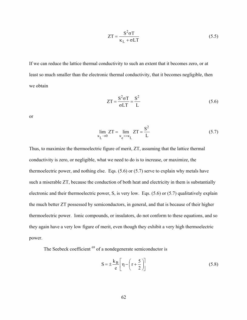
LT
TSZTL
2
σ+κσ
= (5.5)
If we can reduce the lattice thermal conductivity to such an extent that it becomes zero, or at
least so much smaller than the electronic thermal conductivity, that it becomes negligible, then
we obtain
L
SLT
TSZT22
=σσ
= (5.6)
or
L
SZTlimZTlim2
Le0L==
κ>>κ→κ (5.7)
Thus, to maximize the thermoelectric figure of merit, ZT, assuming that the lattice thermal
conductivity is zero, or negligible, what we need to do is to increase, or maximize, the
thermoelectric power, and nothing else. Eqs. (5.6) or (5.7) serve to explain why metals have
such a miserable ZT, because the conduction of both heat and electricity in them is substantially
electronic and their thermoelectric power, S, is very low. Eqs. (5.6) or (5.7) qualitatively explain
the much better ZT possessed by semiconductors, in general, and that is because of their higher
thermoelectric power. Ionic compounds, or insulators, do not conform to these equations, and so
they again have a very low figure of merit, even though they exhibit a very high thermoelectric
power.
The Seebeck coefficient 69 of a nondegenerate semiconductor is
⎥⎦
⎤⎢⎣
⎡⎟⎠⎞
⎜⎝⎛ +−η±=
25r
ekS B (5.8)
62

where η is the reduced Fermi energy, defined by TkTk
E
BB
F ζ==η where EF is the Fermi energy,
kB is the Boltzmann constant and T is the absolute temperature, and r is the scattering parameter
or index that appears in the equation that gives the relaxation time as a function of the energy,
namely , where the reduced Fermi energy is defined as negative when measured
downwards from the edge of the conduction band or upwards from the edge of the valence band,
and where the Fermi energy is positive when measured upwards from the edge of the conduction
band and downwards from the edge of the valence band. Thus both EF and η acquire a zero
value at both edges.
roe Eτ=τ
The Lorenz number 69 of a nondegenerate semiconductor is
⎟⎠⎞
⎜⎝⎛ +⎟
⎠⎞
⎜⎝⎛=
25r
ekL
2B (5.9)
In Eq. (5.8), one may regard –η as the reduced potential energy of the charge carriers and
as the reduced kinetic energy that is transported by the current. Thus, the Peltier
coefficient, equal to ST, represents the total energy transport per unit charge. From Eq. (5.9), we
also see that L is independent of the Fermi energy, provided that the exponent, r, in the energy
dependence of the relaxation time is constant. All of the foregoing statements refer to
nondegenerate semiconductors.
)2/5r( +
Substituting Eqs. (5.8) and (5.9) into Eq. (5.6) we obtain
⎟⎠⎞
⎜⎝⎛ +⎟
⎠⎞
⎜⎝⎛
⎥⎦
⎤⎢⎣
⎡⎟⎠⎞
⎜⎝⎛ +−η⎟
⎠⎞
⎜⎝⎛
=
25r
ek
25r
ek
ZT 2B
22B
(5.10)
thus,
63

25r2
25r
25r
25r
25r2
25r
25r
ZT2
22
2
++η−+
η=
+
⎟⎠⎞
⎜⎝⎛ ++⎟
⎠⎞
⎜⎝⎛ +η−η
=+
⎥⎦
⎤⎢⎣
⎡⎟⎠⎞
⎜⎝⎛ +−η
= (5.11)
Assuming either acoustic-mode lattice scattering or alloy scattering, we may set 21r −= . We
thus have,
222
22
2222
5212
25
21
ZT ⎟⎠
⎞⎜⎝
⎛−
η=+η−
η=+−η−
+−
η= (5.12)
Setting 21r = , which is valid when the bonds are primarily ionic, when scattering is due to the
optical modes, when the interaction between the electrons or holes and the optical modes is not
very strong and when the temperature is well above the Debye temperature ( , we have )DT θ>>
222
33
3232
5212
25
21
ZT ⎟⎟⎠
⎞⎜⎜⎝
⎛−
η=+η−
η=++η−
+
η= (5.13)
Setting 23
=r , which is valid for ionized-impurity scattering, we have
222
22
4242
5232
25
23 ⎟
⎠⎞
⎜⎝⎛ −=+−=++−
+=
ηηηηηZT (5.14)
Eqs. (5.12), (5.13) and (5.14) are algebraic quadratic equations in η. Their roots or eigenvalues
have formed the basis for the construction of the right hand side of Table (2) for nondegenerate
semiconductors.
Now we turn to the degenerate condition when . This means that the Fermi
level is well above the conduction-band edge for electrons or well below the valence-band edge
0k/E BF >>
64

for holes. In other words, the conductor is metallic.
The Seebeck coefficient 69 of a degenerate semiconductor is given by
η
⎟⎠⎞
⎜⎝⎛ +
π= 2
3r
ek
3S B
2m (5.15)
Eq. (5.15) correctly predicts that when 0>>η , S becomes very small which is typical of
metallic conductors. Degenerate semiconductors also behave almost the same way. In order for
a degenerate semiconductor to be able to generate a reasonably high Seebeck coefficient, the
doping level or the free charge carrier concentration must be kept as close as possible to 2.5x10¹⁹
carriers cm-3, which is the maximum value or limit allowed for nondegenerate semiconductors.
The Lorenz number of a degenerate semiconductor is
2
B2
ek
3L ⎟
⎠⎞
⎜⎝⎛π
= (5.16)
Now, substituting Eqs. (5.15) and (5.16) into Eq. (5.6) yields
2
2
2B
2
2
B2
23r
3
ek
3
23r
ek
3
ZT⎟⎟⎟⎟
⎠
⎞
⎜⎜⎜⎜
⎝
⎛
η
+π=
⎟⎠⎞
⎜⎝⎛π
⎥⎥⎥⎥
⎦
⎤
⎢⎢⎢⎢
⎣
⎡
⎟⎟⎟⎟
⎠
⎞
⎜⎜⎜⎜
⎝
⎛
η
+π
=
m
(5.17)
Setting yields 2/1r −=
2
2 13
ZTη
π= (5.18)
Setting yields 2/1r =
2
2 13
4ZTη
π= (5.19)
65

Setting yields 2/3r =
2
23ZTη
π= (5.20)
Now, we know that the Fermi energy has well established values for many materials,
especially elements. Its value for metals and heavily doped degenerate semiconductors can be
obtained from the equation
32
e2
F VN
83
m2hE ⎟
⎠
⎞⎜⎝
⎛π
= (5.21)
where h is Planck’s constant, m is the electronic mass, Ne is the number of electrons up to an
energy, E, and V is the molar volume. The choice of the units of h determines the units of EF.
For heavily doped semiconductors, Eq. (5.21) is still approximately valid. It should be modified,
however, in order to include the linear dependency of η, or EF, on ⎟⎠⎞
⎜⎝⎛ +
23r for degenerate
semiconductors. We thus write
⎟⎠⎞
⎜⎝⎛ +⎟
⎠
⎞⎜⎝
⎛π
=23r
VN
83
m2hE 3
2
e2
F (5.22)
For semiconductors, of course, this assumes that 0=FE at EC, i.e., at the bottom or edge of the
conduction band. It also assumes that 0=FE at EV, i.e., at the top or edge of the valence band.
Let us now investigate the Seebeck coefficient, or thermoelectric power, as given by the
Mott 32 equation
( )
FEEdEElnd
eTk
3S
2B
2
=
σπ= (5.23)
where σ(E) is the electronic conductivity determined as a function of band filling, or Fermi
66
energy, EF. If the electronic scattering is independent of Energy, then σ(E) is just proportional to
the density of states at E. In the general case, S is a measure of the variation in σ(E) above and
below the Fermi surface, specifically through the logarithmic derivative of σ with respect to E.
There is no straightforward or simple way to calculate the logarithmic derivative of σ(E).
Therefore, we will follow a different path in our analysis.
Let us calculate the value of S for certain predetermined values of the dimensionless
thermoelectric figure of merit, ZT, for both degenerate and nondegenerate semiconductors,
assuming that the electronic scattering is not independent of energy, i.e., . We will
thus perform the calculations for
roe Eτ=τ
2/1r −= , 1/2 and 3/2 as usual. We will also assume the
validity of Eq. (5.6). Thus,
( )LZTS2 = (5.24)
or
( ) 2/1ZTLS = (5.25)
We may thus proceed to determine the thermoelectric power required to achieve certain
predetermined values of the dimensionless thermoelectric figure of merit for degenerate and
nondegenerate semiconductors. In order to do that, we need to calculate the Lorenz number,
bearing in mind that its value is constant for degenerate conductors, whereas for nondegenerate
ones, it does depend on r.
The results of these calculations are set forth in Table (1), which gives the Seebeck
coefficient for various values of the dimensionless thermoelectric figure of merit ranging from 1
to 100 for both degenerate and nondegenerate semiconductors.
The basis for performing the calculations of the thermoelectric power set forth in Table
(1) is as follows:
67

(1) For degenerate semiconductors, namely having a free charge carrier concentration more than
2.5x10¹⁹ carriers cm-3, i.e., heavily doped semiconductors, we have used a Lorenz number,
L=2.45x10⁻⁸V2K-2, which is equal to that for metals, and substituted that value into Eq. (5.25).
(2) For nondegenerate semiconductors, namely having a free charge carrier concentration less
than 2.5x10¹⁹ carriers cm-3, i.e., moderately doped and lightly doped semiconductors, we have
used Lorenz number values of 2
Be
k2L ⎟
⎠⎞
⎜⎝⎛= ,
2Be
k3 ⎟
⎠
⎞⎜⎝
⎛ and 2
Be
k4 ⎟
⎠
⎞⎜⎝
⎛ , equal to 1.48x10⁻⁸,
2.22x10⁻⁸ and 2.96x10⁻⁸ V2K-2, corresponding to 2/1r −= , 1/2 and 3/2, respectively. These
values were once more substituted into Eq. (5.25). Furthermore, the basis for calculating those
Lorenz numbers has been Eq. (5.9).
TABLE 1. Values of the thermoelectric power, S, μVK-1.
DegenerateSemiconductors
ZT -1/2 1/2 3/2157 122 149 172221 172 211 243271 211 258 298313 243 298 344350 272 333 385495 385 471 544700 544 666 769857 666 816 942990 769 942 10881107 860 1054 12171212 942 1154 13331310 1018 1247 14391400 1088 1333 15391485 1154 1414 16321565 1217 1490 1720
90100
S
50607080
10203040
2345
NondegenerateSemiconductors
r
1
Carrying on with this analysis, we now consider the following equations:
68

1
FxTe
xTE
e1
Te1S
−
⎥⎦⎤
⎢⎣⎡∂∂
∂ζ∂
=∂∂
±=∂ζ∂
±= (5.26)
( ) ( ) ( )η⎟⎠⎞
⎜⎝⎛ +Γτ⎟
⎠⎞
⎜⎝⎛π=σ + exp
25rTk*me
h2
38
23r
Bo21
223
2 (5.27)
where Г is the gamma function.
E8
kh*m 2
22
π= (5.28)
which is the same expression as for a free-electron gas, except that the electronic mass, m, has
been replaced by m*, the effective mass.
( ) 2/12/1
E22hk*mπ
= (5.29)
FEEdEd1
eTk
3FEEdE
lndeTk
3S
2B
22B
2
=
σσ
π=
=
σπ= (5.30)
( )T
ZTLke3
TS
ke3
FEEdEd 2/1
2B
22B
2σ
π=
σ
π=
=
σ (5.31)
Therefore,
( ) ( )Tk
125rZT3
25r
ek
TZT
ke3
FEEdElnd
B
21
21
221
B2/1
2B
2 ⎟⎠⎞
⎜⎝⎛ +
π=⎟
⎠⎞
⎜⎝⎛ +
π=
=
σ (5.32)
The above result applies to degenerate semiconductors and assumes the validity of Eq. (5.6).
Thus, Eq. (5.32) gives the logarithmic derivative of σ with respect to E at the Fermi surface in
terms of a constant multiplied by the reciprocal of the product of the Boltzmann constant and the
temperature. Substitution of Eq. (5.32) into Eq. (5.30) yields
69
( )e
k25rZTS B2
121
⎟⎠⎞
⎜⎝⎛ += (5.33)
The Seebeck coefficient is given by a constant multiplied by the Boltzmann constant, divided by
the electronic charge. Eq. (5.33) is thus dimensionally correct, since it gives S as VK-1, the way
it should be. The constants involved in both Eqs. (5.32) and (5.33), actually depend on ZT. The
higher S is, the higher ZT will be.
One can now use Eq. (5.26) to determine the Fermi energy as a function of the
temperature. One thus obtains
eSdTd ±=ζ (5.34)
( )∫∫∫ ⎟⎠⎞
⎜⎝⎛ +±=±=ζ dTk
25rZTeSdTd B
21
21
or
( ) +⎟⎠⎞
⎜⎝⎛ +±==ζ Tk
25rZTE B
21
21
F constant (5.35)
Now we will take an alternative and different approach in order to obtain S, using Eqs.
(5.27), (5.28), (5.29) and (5.30). We will thus proceed as follows
( ) ( )
( ) ( )
⎟⎠⎞
⎜⎝⎛−
η⎟⎠⎞
⎜⎝⎛ +Γτ
π⎟⎠⎞
⎜⎝⎛π
η⎟⎠⎞
⎜⎝⎛ +Γτ
π⎟⎠⎞
⎜⎝⎛π
=σ −
+
+
1
23r
Bo22
3
2
23r
Bo22
3
2E
21
exp25rTk
22hke
h2
38
exp25rTk
22hke
h2
38
dElnd (5.36)
consequently,
FE2
1
FEEdElnd
−==
σ (5.37)
70

and finally
F
2B
2
F
2B
2
E1
eTk
6E21
eTk
3S π
−=⎟⎟⎠
⎞⎜⎜⎝
⎛−
π= (5.38)
or
η
π−=
1e
k6
S B2
(5.39)
where is the reduced Fermi energy. Tk/E BF=η
It should be pointed out that Eq. (5.27) gives the electrical conductivity for a
nondegenerate semiconductor. Eqs. (5.38) or (5.39) thus give the thermoelectric power of a
nondegenerate semiconductor, according to Eq. (5.23), established by Mott 32.
Proceeding now to investigate the degenerate condition, we know that the electrical
conductivity of a degenerate conductor is given by
( ) 2/3ro
2/1223
2 *meh2
38 +ζτ⎟
⎠⎞
⎜⎝⎛π=σ (5.40)
which, along with Eqs. (5.28) and (5.29), yields
⎟⎠⎞
⎜⎝⎛−
ζτπ
⎟⎠⎞
⎜⎝⎛π
ζτπ
⎟⎠⎞
⎜⎝⎛π
=σ −
+
+
1
2/3ro
223
2
2/3ro
223
2E
21
22hke
h2
38
22hke
h2
38
dElnd (5.41)
thus
FF
E21
EEdElnd
−==
σ (5.42)
therefore, substituting the above result into Eq. (5.30), yields
71
F
2B
2
E1
eTk
6S π
−= (5.43)
or
η
π−=
1e
k6
S B2
(5.44)
where Tk/Tk/E BBF ζ==η is the reduced Fermi energy. This is the same result as that
obtained from Eqs. (5.38) and (5.39). We thus conclude that Eq. (5.30), also known as the
Mott32 equation, gives the same thermoelectric power for any semiconductor condition,
regardless of whether it is degenerate or nondegenerate.
We may now use Eq. (5.6) to obtain the dimensionless thermoelectric figure of merit, ZT,
substituting the thermoelectric power, S, as given by the Mott equation, i.e., either Eq. (5.43) or
(5.44). The Lorenz number, L, has to be carefully evaluated, however, since we no longer have a
unique expression for it, as was the case for S. The only way to obtain the Lorenz number must
be based on the Goldsmid analysis, which distinguishes between degenerate and nondegenerate
semiconductors. Furthermore, in the case of a nondegenerate semiconductor, the value of L will
also vary, depending on the scattering parameter, r. Thus, for the broad-spectrum of
semiconductors in general, we are going to have different values for the Mott ZT, bearing the
aforementioned variables in mind.
For degenerate semiconductors, we thus have
2
2
2
2B
2
22
2B
4
112
ek
3
1ek
36ZT
η
π=
π
η
π
= (5.45)
The above result is the Mott dimensionless thermoelectric figure of merit for degenerate
72

conductors.
For nondegenerate semiconductors, we obtain the following equations, depending on the
respective values of r. Thus, for 2/1r −=
2
4
2
2B
22
2B
4
172
ek2
1ek
36ZT
η
π=η
π
= (5.46)
for 2/1r =
2
4
2
2B
22
2B
4
1108
ek3
1ek
36ZT
η
π=η
π
= (5.47)
for 2/3r =
2
4
2
2B
22
2B
4
1144
ek4
1ek
36ZT
η
π=η
π
= (5.48)
We will now use Eqs. (5.12), (5.13) and (5.14), to calculate the reduced Fermi energy, η,
of nondegenerate semiconductors, for appropriate values of the scattering parameter, r, and
values of the dimensionless thermoelectric figure of merit, ZT, ranging from 1 to 100. We will
also use Eqs. (5.18), (5.19) and (5.20) to calculate η for degenerate semiconductors for the same
values of r and ZT. All of the aforementioned equations are based on the original formulation by
Goldsmid for the Seebeck coefficient and the Lorenz number. The results of these calculations
are presented in Table (2). Table (3) contains the corresponding values of η based on the Mott
formulation.
73
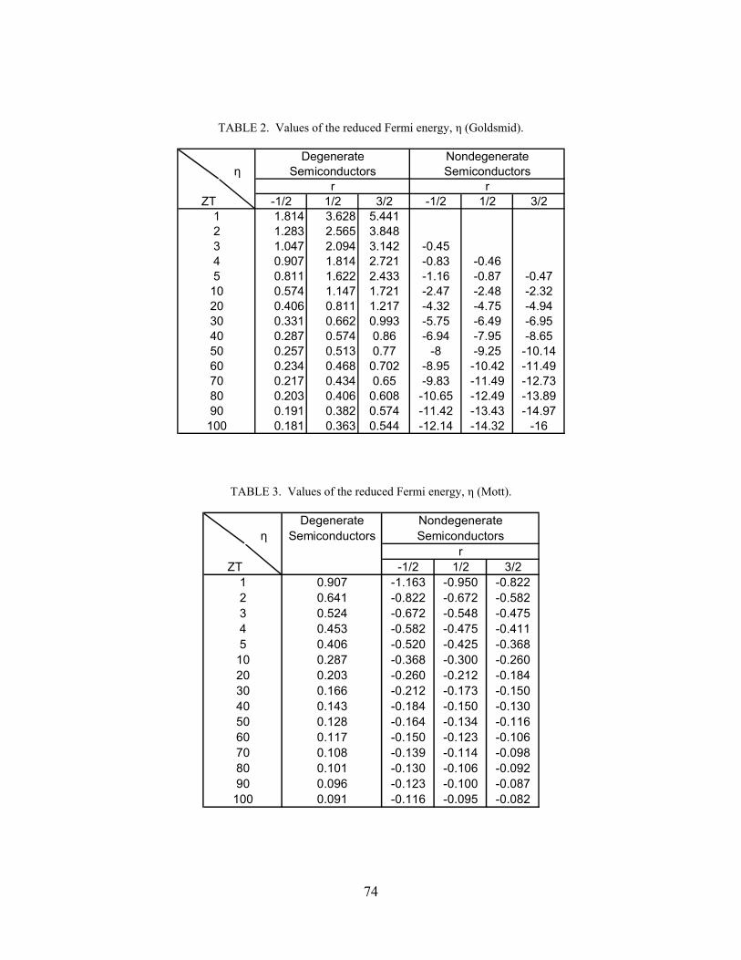
TABLE 2. Values of the reduced Fermi energy, η (Goldsmid).
ZT -1/2 1/2 3/2 -1/2 1/2 3/21.814 3.628 5.4411.283 2.565 3.8481.047 2.094 3.142 -0.450.907 1.814 2.721 -0.83 -0.460.811 1.622 2.433 -1.16 -0.87 -0.470.574 1.147 1.721 -2.47 -2.48 -2.320.406 0.811 1.217 -4.32 -4.75 -4.940.331 0.662 0.993 -5.75 -6.49 -6.950.287 0.574 0.86 -6.94 -7.95 -8.650.257 0.513 0.77 -8 -9.25 -10.140.234 0.468 0.702 -8.95 -10.42 -11.490.217 0.434 0.65 -9.83 -11.49 -12.730.203 0.406 0.608 -10.65 -12.49 -13.890.191 0.382 0.574 -11.42 -13.43 -14.970.181 0.363 0.544 -12.14 -14.32 -16
90100
η
50607080
10203040
2345
NondegenerateSemiconductors
r
1
DegenerateSemiconductors
r
TABLE 3. Values of the reduced Fermi energy, η (Mott).
DegenerateSemiconductors
ZT -1/2 1/2 3/20.907 -1.163 -0.950 -0.8220.641 -0.822 -0.672 -0.5820.524 -0.672 -0.548 -0.4750.453 -0.582 -0.475 -0.4110.406 -0.520 -0.425 -0.3680.287 -0.368 -0.300 -0.2600.203 -0.260 -0.212 -0.1840.166 -0.212 -0.173 -0.1500.143 -0.184 -0.150 -0.1300.128 -0.164 -0.134 -0.1160.117 -0.150 -0.123 -0.1060.108 -0.139 -0.114 -0.0980.101 -0.130 -0.106 -0.0920.096 -0.123 -0.100 -0.0870.091 -0.116 -0.095 -0.082
NondegenerateSemiconductors
r
1
203040
2345
90100
η
50607080
10
74
Now, the following comments are noteworthy regarding Tables (2) and (3). With reference to
Table (2), we observe that the values of the reduced Fermi energy, η, for degenerate
semiconductors are related to one another in the ratio of 1:2:3, corresponding to ,
and , respectively, and that is, of course, for the same ZT value. These η values are all
positive and they start either pointing upwards from the edge of the conduction band, or pointing
downwards from the edge of the valence band. The zero values of the Fermi energy coincide
with either of these two edges, with the forbidden energy band gap being enclosed between
them. We thus also observe that as the value of the dimensionless thermoelectric figure of merit,
ZT, gets higher and higher, the reduced Fermi energy gets lower and lower. This, obviously,
agrees with the fact that metals, which have a negligible ZT, also possess a Fermi energy that is
much higher than that of semiconductors. Thus, the only way to get an infinite ZT is to reduce
the reduced Fermi energy to zero. Thus, when performing the calculations for the reduced Fermi
energy, η, only the positive answers were accepted, while the negative ones were rejected.
Obviously, therefore, all Fermi energy levels for degenerate semiconductors must lie either
within the conduction band or the valence band, they cannot be in the forbidden band gap. In
contrast, the reduced Fermi energy levels for nondegenerate semiconductors are all located
within the forbidden energy band gap, outside both the conduction and valence bands. These η
values, or levels, are all negative and they either start pointing downwards from the edge of the
conduction band, or pointing upwards from the edge of the valence band. Thus the zero values
of the Fermi energy for nondegenerate semiconductors must coincide with either the edge of the
conduction band or the edge of the valence band. For a semiconductor to be considered
nondegenerate, it is necessary that
2/1r −= 2/1
2/3
0Tk/E BF << , i.e., the Fermi level lies within the forbidden
gap well away from the appropriate band edge. The nondegenerate approximation is very good
75
when and is still acceptable for many purposes when Tk4E BF −< Tk2E BF −< . It is
necessary that the Fermi level should be much further from the opposite band edge, if minority
carriers are to be neglected. In order to assure this, it is, therefore, necessary that we choose or
design materials having a sufficiently wide forbidden energy band gap. This fact is crucially
important, if we want to develop materials with superior thermoelectric properties and
performance.
Table (2) contains values of the reduced Fermi energy, η, for different values of r and ZT,
for both degenerate and nondegenerate semiconductors. The calculations of the η values for
degenerate semiconductors were rather straightforward, whereas those for nondegenerate
semiconductors involved solving and obtaining the roots or eigenvalues of forty five algebraic
quadratic equations. Only the negative eigenvalues were selected, since that agrees with the
original assumption that the semiconductor is nondegenerate and, as such, its Fermi energy can
only acquire a negative value.
Table (3) contains the values of η, obtained according to the Mott formulation. For
degenerate semiconductors, there is a single η value for each ZT one, regardless of that of r.
Looking at the Mott data, we clearly see that they can be reconciled with the corresponding ones
given in Table (2), for , if we multiply the former by a factor of 2. And that is because
the thermoelectric power, S, obtained according to the Mott formulation, namely Eq. (5.39), is
one half that given by the Goldsmid formulation, namely Eq. (5.15), for . That would
justify multiplying the original Mott equation for S by a correction factor of 2. As for
nondegenerate semiconductors, the Mott data leave a lot to be desired. All the η values are in
flagrant violation of the simple, but very basic, rule that η be at least <-2, so that the Fermi level
within the forbidden band gap be well away from the appropriate band edge. For both of the
2/1r −=
2/1r −=
76
aforementioned reasons, Mott’s data and formulation are by no means considered credible or
useful. This, of course, leaves Table (2) as the only viable basis for any further research on this
subject.
Regardless of the above criticism of Mott’s formulation and data, as expressed by Eq.
(5.39) and Table (3), it is probably more constructive to look more closely into the reasons for
the discrepancy in the data pertaining to Tables (2) and (3). We are specifically referring to the
disagreement between the η values as presented in these two tables, for degenerate
semiconductors.
As stated earlier, if the data presented in the left column of Table (3), for degenerate
semiconductors, get multiplied by a factor of 2, the discrepancy between them and the
corresponding ones given in Table (2), again for degenerate semiconductors, for , is
entirely removed. The two sets of data become identical. This means that the original Mott
equation for the Seebeck coefficient must be multiplied by a correction factor of 2. Doing this,
Eq. (5.30) then becomes
2/1−=r
η
π=
π=
=
σπ=
1e
k3E
1eTk
3EEdElnd
eTk
32S B
2
F
2B
2
F
2B
2 (5.49)
Having introduced the above correction factor, yields
η
π==
1e
k3
SS B2
GM (5.50)
or
( ) 2/1
B2
B2
GMZTL
1e
k3S
1e
k3
π=
π=η=η (5.51)
where M and G denote Mott and Goldsmid, respectively. Applying the aforementioned
correction factor implies that the earlier Eqs. (5.45), (5.46), (5.47) and (5.48) must also be
77

modified and rewritten. The new equations are thus expressed as follows:
For degenerate semiconductors
2
2
2
2B
2
22
2B
4
13
e
k3
1e
k9
ZTη
π=
π
η
π
= (5.52)
For nondegenerate semiconductors, with 2/1r −=
2
4
2
2B
22
2B
4
118
e
k2
1e
k9
ZTη
π=η
π
= (5.53)
For nondegenerate semiconductors, with 2/1r =
2
4
2
2B
22
2B
4
127
e
k3
1e
k9
ZTη
π=η
π
= (5.54)
For nondegenerate semiconductors, with 2/3r =
2
4
2
2B
22
2B
4
136
e
k4
1e
k9
ZTη
π=η
π
= (5.55)
The above four equations can be further worked out to give the reduced Fermi energy, η,
directly according to the Mott formulation. We thus have
For degenerate semiconductors
ZT3Mπ
=η (5.56)
For nondegenerate semiconductors, with 2/1r −=
78

ZT23
2
Mπ−
=η (5.57)
For nondegenerate semiconductors, with 2/1r =
ZT33
2
Mπ−
=η (5.58)
For nondegenerate semiconductors, with 2/3r =
ZT6
2
Mπ−
=η (5.59)
We may now proceed to introduce all of the above modifications and reconstruct Table
(3), which will become Table (4), and which will be included at the end of this discussion.
Considering now Mott’s formula in its modified form, namely Eq. (5.49), we notice from Table
(4) that it now gives reliable values for the reduced Fermi energy for degenerate semiconductors
for which . For other values of r, namely 1/2 and 3/2, it does not yield any answers,
because it is not related to the scattering parameter, r, in any way whatsoever. Furthermore,
despite the modification already made, it still does not give reliable and acceptable values for the
reduced Fermi energy of nondegenerate semiconductors, no matter what the value of r is. It is
thus quite evident that Mott’s equation generally does not apply to nondegenerate
semiconductors.
2/1r −=
We therefore finally conclude that the Mott equation does not yield any quantitatively
correct values for the Seebeck coefficient or for the reduced Fermi energy, resulting therefrom,
regardless of whether the semiconductor is degenerate or nondegenerate, and regardless of what
the value of the scattering parameter or index is, since Mott’s formulation does not take account
of the scattering parameter. It is, nevertheless, worthwhile or useful qualitatively, since it
provides a good physical picture of the nature of the Seebeck coefficient, presenting it as
79

fundamentally proportional to the derivative of the electrical conductivity with respect to the
energy evaluated at the Fermi surface in the Brillouin space.
TABLE 4. Modified Values of the reduced Fermi energy, η (Mott).
DegenerateSemiconductors
ZT -1/2 1/2 3/21.814 -2.326 -1.900 -1.6441.283 -1.644 -1.344 -1.1641.047 -1.344 -1.096 -0.9500.907 -1.164 -0.950 -0.8220.811 -1.040 -0.850 -0.7360.574 -0.736 -0.600 -0.5200.406 -0.520 -0.424 -0.3680.331 -0.424 -0.346 -0.3000.287 -0.368 -0.300 -0.2600.257 -0.328 -0.268 -0.2320.234 -0.300 -0.246 -0.2120.217 -0.278 -0.228 -0.1960.203 -0.260 -0.212 -0.1840.191 -0.246 -0.200 -0.1740.181 -0.232 -0.190 -0.164
90100
ηM
50607080
10203040
2345
NondegenerateSemiconductors
r
1
80

Chapter 6
Critical Analysis of the Thermoelectric Figure of
Merit as Related to the Wiedemann-Franz and
Eucken Laws
It is now appropriate to carry out a critical review of Eq. (5.6) with the objective of
determining the conditions under which the equation may or may not be valid. Writing this
equation once more, we have
ZTlimZTlimL
S
Le0L
2
κ>>κ→κ== (6.1)
Although κL can always be reduced through mass-and volume-fluctuation scattering, or alloy
scattering, also known as lattice point-defect scattering, the use of rattlers, quantum wells,
superlattices and clathrates, or the use of Glen Slack’s concept of the phonon glass, which is
essentially an amorphous material in which crystallinity is completely destroyed through the
creation of a generalized disorder in the lattice, yet κL no matter how small it is, or how great the
disorder is, never becomes exactly equal to zero. Rewriting Eq. (6.1), we have
L
SLT
TSTSTSlimTSlim22
e
2
eL
2
LeeL
2
0L=
σσ
=κσ
=κ+κ
σ=
κ+κσ
κ>>κ→κ (6.2)
Now considering only the denominator in the above equation, yields
⎟⎟⎠
⎞⎜⎜⎝
⎛κκ
+κ=κ+κL
eLeL 1 (6.3)
In order for , then Le κ>>κ
81

1L
e >>κκ
(6.4)
If , then the limiting value of Eq. (6.3) becomes ( ) 1/ Le >>κκ
( ) ( ) ( ) ( ) eL
eL
L
e1L/e
LL
eL
1L/eeL
1L/e1lim1limlim κ=
κκ
κ=⎟⎟⎠
⎞⎜⎜⎝
⎛κκ
+κ=⎟⎟⎠
⎞⎜⎜⎝
⎛κκ
+κ=κ+κ>>κκ>>κκ>>κκ
(6.5)
Thus, in order to ensure the validity of Eqs. (5.6) or (6.2), we have to assure that inequality (6.4)
is satisfied, i.e.,
1L
e >>κκ
The above inequality, although apparently simplistic, yet provides a powerful means or criterion
that enables us to investigate the domain of validity of Eq. (5.6) on a rather rigorous basis.
We will now proceed to derive a theoretical expression giving the value of the ratio
between the electronic and lattice components of the thermal conductivity. In doing so, we will
invoke the following two laws, which are well known in physics:
(1) The Wiedemann-Franz law, already referred to several times in this dissertation.
(2) The Eucken law 12, which states that for pure dielectric crystals the thermal conductivity
varies inversely with the absolute temperature. Debye found that by taking account of the
anharmonic nature of forces in real crystals, thermal conductivity takes on finite values. In
effect, the elastic constants of a substance vary from point to point according to the local
displacements of the atoms. Variation in either the density or the elastic properties are
responsible for scattering the vibrational waves and, thus, for limiting the value of the thermal
conductivity. Peierls showed how the anharmonicity of the lattice vibrations could be taken into
account by introducing the concept of phonon wave packets that arise from the quantization of
82

vibrational waves. These wave packets are now simply referred to as phonons, and they may be
regarded as the energy carriers that are responsible for heat conduction by the lattice. A limit on
thermal conductivity is set by phonon collisions that do not conserve momentum. The thermal
conductivity that we are referring to is actually the phonon or lattice component of the total
thermal conductivity. Thus, if κL is used to denote the lattice thermal conductivity, then it may
be expressed as
(6.6) 1L AT−=κ
where A is a constant. The above equation is Eucken’s law for the lattice thermal conductivity,
and holds when . It is known to be particularly true for semiconductors in which the
chemical bonding is of the covalent-ionic type, specifically alloys or solid solutions of
intermetallic compounds in which mass and volume fluctuation scattering, also known as alloy
scattering, prevails, and is normally used to reduce the lattice thermal conductivity.
DT θ>
Let us now take a look at the electronic component of the thermal conductivity.
According to the Wiedemann-Franz law, it is expressed as
LTe σ=κ (6.7)
The electrical conductivity, σ, for nondegenerate semiconductors is given by Eq. (5.27), which
comprises a number of parameters, or quantities, that are outright constants, as well as other
parameters which are not exactly constants, yet may be regarded as such, according to the way
we are carrying out this analysis. We are explicitly trying to find out the degree of dependency
of the electrical conductivity on the two variables that are crucially important in controlling the
thermoelectric performance of semiconducting materials. These are the absolute temperature, T,
and the free charge carrier concentration, n. To enable us to do so, we invoke Eq. (5.21) and use
it to express the reduced Fermi energy in terms of the concentration of the free charge carriers
83
and the temperature even though we know that it is only valid for metals and approximately valid
for heavily doped degenerate semiconductors. This will be our preliminary, or first, attempt to
establish a theoretical correlation of the electronic to lattice thermal conductivity ratio as a
function of free charge carrier concentration and temperature.
Thus, the electrical conductivity for nondegenerate semiconductors can be expressed as
follows
( ) ( )⎥⎥⎦
⎤
⎢⎢⎣
⎡⎟⎠⎞
⎜⎝⎛π
⎟⎠⎞
⎜⎝⎛ +Γτ⎟
⎠⎞
⎜⎝⎛π=σ +
Tkn
83
m2hexp
25rTk*me
h2
38
B
3/23/222/3r
Bo2/12
2/3
2 (6.8)
( ) ( )⎥⎥⎦
⎤
⎢⎢⎣
⎡⎟⎠⎞
⎜⎝⎛π
⎟⎠⎞
⎜⎝⎛ +Γτ⎟
⎠⎞
⎜⎝⎛π= +
Tn3
mk8hexp
25rTk*me
h2
38 3/23/2
B
22/3r
Bo2/12
2/3
2 (6.9)
( ) ( )⎥⎥⎦
⎤
⎢⎢⎣
⎡⎟⎠⎞
⎜⎝⎛ +Γτ⎟
⎠⎞
⎜⎝⎛π= +
TnAexp
25rTk*me
h2
38 3/2
2/3rBo
2/122/3
2 (6.10)
where
( ) Km1023156822.4338066.110953.98
1010101062618.63mk8hA 211
3/2423316823/2
B
2−
−×=⎟
⎠⎞
⎜⎝⎛π××
××××=⎟
⎠⎞
⎜⎝⎛π
=
(6.11)
The exponential term in the above Eqs. (6.8), (6.9) or (6.10) actually stands for eη. Its
magnitude has been calculated for various values of the free charge carrier concentration, n, and
the temperature, T, and the results are given in Table (5). The corresponding values of the
reduced Fermi energy, , have also been calculated and presented in Table (6) Tk/E BF=η
84

TABLE 5. Values of the exponential term, eη, in Eq. (6.8) for nondegenerate semiconductors.
1018 1019
carriers cm-3 carriers cm-3
1.151485 1.9246751.088316 1.4812021.043224 1.217047
n
300 KT
500 K1000 K
TABLE 6. Reduced Fermi energy, η, according to Eqs. (6.8)-(6.10), as well as Table (5), for nondegenerate
semiconductors.
1018 1019
carriers cm-3 carriers cm-3
0.1411 0.65480.0846 0.39290.0423 0.1964
n
300 KT
500 K1000 K
Now, a critical study of the above Eqs., (6.8)-(6.11), reveals the following:
(1) There is a direct proportionality between the electrical conductivity, σ, and the free charge
carrier concentration, n. This dependentcy, however, is somewhat weakened due to the fact that
n is raised to the power 2/3.
(2) The quantity, n, aside from being so reduced in value, is also included as part of the index of
an exponential function, along with a constant, A, whose value is enormously small, of the order
of 10-11, which further reduces its effect on the magnitude of the electrical conductivity.
(3) Most importantly, the Fermi energy is given by Eq. (5.21) as a positive quantity. This
cannot be tolerated or accepted, because we already know that for nondegenerate semiconductors
the Fermi energy lies within the forbidden energy band gap, and is always measured downwards
from the edge of the conduction band or upwards from the edge of the valence band, and as such
it can only have negative values. If we attempt to introduce a negative sign into the argument of
the exponential term in Eq. (6.8), then eη will have to move to the denominator of that equation.
85
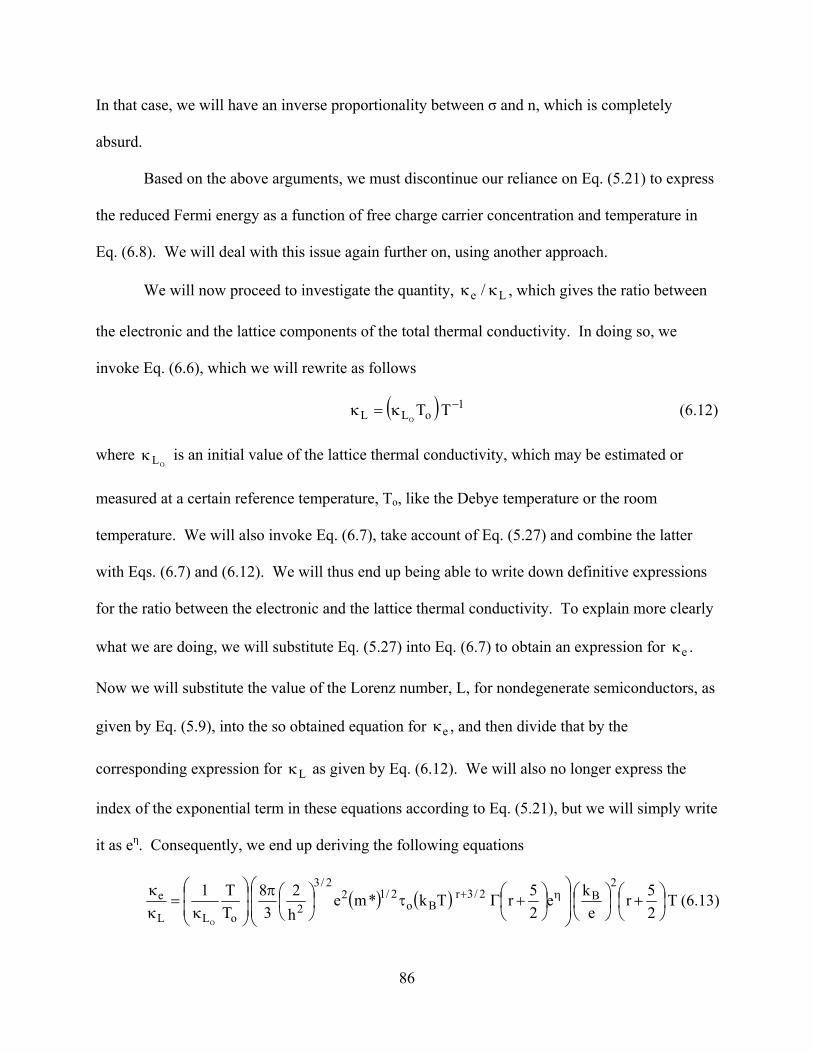
In that case, we will have an inverse proportionality between σ and n, which is completely
absurd.
Based on the above arguments, we must discontinue our reliance on Eq. (5.21) to express
the reduced Fermi energy as a function of free charge carrier concentration and temperature in
Eq. (6.8). We will deal with this issue again further on, using another approach.
We will now proceed to investigate the quantity, Le / κκ , which gives the ratio between
the electronic and the lattice components of the total thermal conductivity. In doing so, we
invoke Eq. (6.6), which we will rewrite as follows
( ) 1oLL TT
O
−κ=κ (6.12)
where is an initial value of the lattice thermal conductivity, which may be estimated or
measured at a certain reference temperature, To, like the Debye temperature or the room
temperature. We will also invoke Eq. (6.7), take account of Eq. (5.27) and combine the latter
with Eqs. (6.7) and (6.12). We will thus end up being able to write down definitive expressions
for the ratio between the electronic and the lattice thermal conductivity. To explain more clearly
what we are doing, we will substitute Eq. (5.27) into Eq. (6.7) to obtain an expression for
OLκ
eκ .
Now we will substitute the value of the Lorenz number, L, for nondegenerate semiconductors, as
given by Eq. (5.9), into the so obtained equation for eκ , and then divide that by the
corresponding expression for as given by Eq. (6.12). We will also no longer express the
index of the exponential term in these equations according to Eq. (5.21), but we will simply write
it as eη. Consequently, we end up deriving the following equations
Lκ
( ) ( ) T25r
eke
25rTk*me
h2
38
TT1 2
B2/3rBo
2/122/3
2oLL
e
O
⎟⎠⎞
⎜⎝⎛ +⎟
⎠⎞
⎜⎝⎛
⎟⎟
⎠
⎞
⎜⎜
⎝
⎛⎟⎠⎞
⎜⎝⎛ +Γτ⎟
⎠⎞
⎜⎝⎛π
⎟⎟⎠
⎞⎜⎜⎝
⎛
κ=
κκ η+ (6.13)
86

or
( ) ( ) ⎟⎠⎞
⎜⎝⎛ +
⎟⎟
⎠
⎞
⎜⎜
⎝
⎛⎟⎠⎞
⎜⎝⎛ +Γτ⎟
⎠⎞
⎜⎝⎛π
⎟⎟⎠
⎞⎜⎜⎝
⎛
κ=
κκ η+
25re
25rTk*m
h2
38
T1 2/7r
Bo2/1
2/3
2oLL
e
O
(6.14)
For 2/1r −=
( ) ( )⎟⎟
⎠
⎞
⎜⎜
⎝
⎛τ⎟
⎠
⎞⎜⎝
⎛π⎟⎟⎠
⎞⎜⎜⎝
⎛
κ=
κκ ηeTk*m
h2
316
T1 3
Bo2/1
2/3
2oLL
e
O
(6.15)
For 2/1r =
( ) ( )⎟⎟
⎠
⎞
⎜⎜
⎝
⎛τ⎟
⎠
⎞⎜⎝
⎛π⎟⎟⎠
⎞⎜⎜⎝
⎛
κ=
κκ ηeTk*m
h216
T1 4
Bo2/1
2/3
2oLL
e
O
(6.16)
For 2/3r =
( ) ( )⎟⎟
⎠
⎞
⎜⎜
⎝
⎛τ⎟
⎠
⎞⎜⎝
⎛π⎟⎟⎠
⎞⎜⎜⎝
⎛
κ=
κκ ηeTk*m
h264
T1 5
Bo2/1
2/3
2oLL
e
O
(6.17)
In the foregoing equations for nondegenerate semiconductors, it is worthwhile to
introduce the free charge carrier concentration, n, instead of exp(η). We thus make use of the
relationship
( ) ( ) ( )η⎟⎠⎞
⎜⎝⎛ π
== ∫∞
exph
Tk*m22dEEgEfn 2
3
2B
0 (6.18)
which yields
( ) 23
2B
hTk*m2
2neexp
−η ⎟
⎠
⎞⎜⎝
⎛ π==η (6.19)
This is preferable from the practical point of view, since the free charge carrier concentration is
the independent variable that can be directly controlled, at least for semiconducting materials.
We thus rewrite both Eqs. (5.27) and (6.8), as follows
87
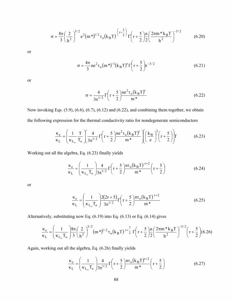
( ) ( )2/3
2B2
3r
Bo2/12
2/3
2 hTk*m2
2n
25rTk*me
h2
38 −⎟
⎠⎞
⎜⎝⎛ +
⎟⎠⎞
⎜⎝⎛ π
⎟⎠⎞
⎜⎝⎛ +Γτ⎟
⎠⎞
⎜⎝⎛π=σ (6.20)
or
( ) ( ) 2/3rB
1o
2
25rTk*mne
34 −− π⎟
⎠⎞
⎜⎝⎛ +Γτ
π=σ (6.21)
or
( )*m
Tkne25r
34 r
Bo2
2/1τ
⎟⎠⎞
⎜⎝⎛ +Γ
π=σ (6.22)
Now invoking Eqs. (5.9), (6.6), (6.7), (6.12) and (6.22), and combining them together, we obtain
the following expression for the thermal conductivity ratio for nondegenerate semiconductors
( )
T25r
ek
*mTkne
25r
34
TT1 2
Br
Bo2
2/1oLL
e
O⎟⎟
⎠
⎞
⎜⎜
⎝
⎛⎟⎠⎞
⎜⎝⎛ +⎟
⎠⎞
⎜⎝⎛
⎟⎟⎠
⎞⎜⎜⎝
⎛ τ⎟⎠⎞
⎜⎝⎛ +Γ
π⎟⎟⎠
⎞⎜⎜⎝
⎛
κ=
κκ
(6.23)
Working out all the algebra, Eq. (6.23) finally yields
( )
⎟⎠⎞
⎜⎝⎛ +
τ⎟⎠⎞
⎜⎝⎛ +Γ
π⎟⎟⎠
⎞⎜⎜⎝
⎛
κ=
κκ +
25r
*mTkn
25r
34
T1 2r
Bo2/1
oLL
e
O
(6.24)
or
( ) ( )*mTkn
25r
35r22
T1 2r
Bo2/1
oLL
e
O
+τ⎟⎠⎞
⎜⎝⎛ +Γ
π
+⎟⎟⎠
⎞⎜⎜⎝
⎛
κ=
κκ
(6.25)
Alternatively, substituting now Eq. (6.19) into Eq. (6.13) or Eq. (6.14) gives
( ) ( ) ⎟⎠⎞
⎜⎝⎛ +⎟
⎠
⎞⎜⎝
⎛ π⎟⎠⎞
⎜⎝⎛ +Γτ⎟
⎠
⎞⎜⎝
⎛π⎟⎟⎠
⎞⎜⎜⎝
⎛
κ=
κκ −
+
25r
hTk*m2
2n
25rTk*m
h2
38
T1 2/3
2B
27r
Bo2/1
2/3
2oLL
e
O
(6.26)
Again, working out all the algebra, Eq. (6.26) finally yields
( )
⎟⎠⎞
⎜⎝⎛ +
τ⎟⎠⎞
⎜⎝⎛ +Γ
π⎟⎟⎠
⎞⎜⎜⎝
⎛
κ=
κκ +
25r
*mTkn
25r
34
T1 2r
Bo2/1
oLL
e
O
(6.27)
88
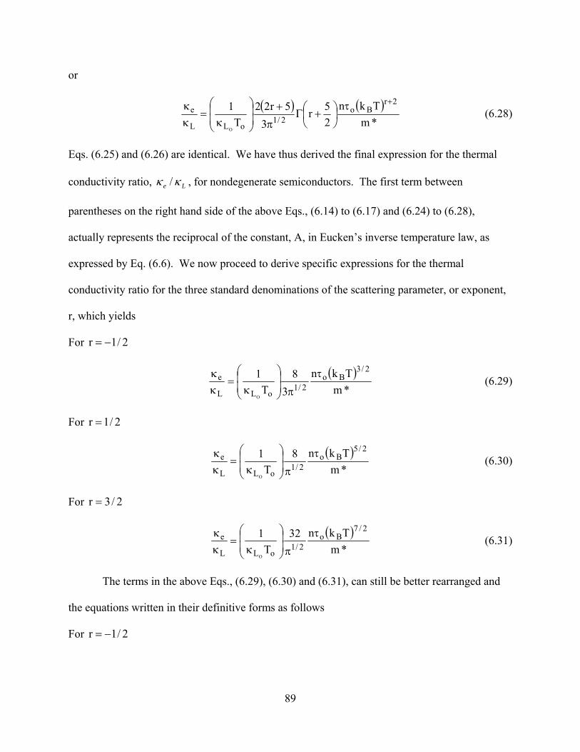
or
( ) ( )*mTkn
25r
35r22
T1 2r
Bo2/1
oLL
e
O
+τ⎟⎠⎞
⎜⎝⎛ +Γ
π
+⎟⎟⎠
⎞⎜⎜⎝
⎛
κ=
κκ
(6.28)
Eqs. (6.25) and (6.26) are identical. We have thus derived the final expression for the thermal
conductivity ratio, Le κκ / , for nondegenerate semiconductors. The first term between
parentheses on the right hand side of the above Eqs., (6.14) to (6.17) and (6.24) to (6.28),
actually represents the reciprocal of the constant, A, in Eucken’s inverse temperature law, as
expressed by Eq. (6.6). We now proceed to derive specific expressions for the thermal
conductivity ratio for the three standard denominations of the scattering parameter, or exponent,
r, which yields
For 2/1r −=
( )
*mTkn
38
T1 2/3
Bo2/1
oLL
e
O
τ
π⎟⎟⎠
⎞⎜⎜⎝
⎛
κ=
κκ
(6.29)
For 2/1r =
( )
*mTkn8
T1 2/5
Bo2/1
oLL
e
O
τ
π⎟⎟⎠
⎞⎜⎜⎝
⎛
κ=
κκ
(6.30)
For 2/3r =
( )
*mTkn32
T1 2/7
Bo2/1
oLL
e
O
τ
π⎟⎟⎠
⎞⎜⎜⎝
⎛
κ=
κκ
(6.31)
The terms in the above Eqs., (6.29), (6.30) and (6.31), can still be better rearranged and
the equations written in their definitive forms as follows
For 2/1r −=
89

2/32/3
Bo2/1
oLL
e nT*m
k3
8T
1
O
τ
π⎟⎟⎠
⎞⎜⎜⎝
⎛
κ=
κκ
(6.32)
For 2/1r =
2/52/5
Bo2/1
oLL
e nT*m
k8T
1
O
τ
π⎟⎟⎠
⎞⎜⎜⎝
⎛
κ=
κκ
(6.33)
For 2/3r =
2/72/7
Bo2/1
oLL
e nT*m
k32T
1
O
τ
π⎟⎟⎠
⎞⎜⎜⎝
⎛
κ=
κκ
(6.34)
The electrical conductivity of degenerate semiconductors is given by Eq. (5.40).
Invoking now Eq. (5.22) and using it to express the Fermi energy in terms of the concentration of
the free charge carriers, we can rewrite Eq. (5.40) as follows
( ) 23r2
3r
32
2
o2/122
3
2 23rn
83
m2h*me
h2
38 +
+
⎟⎠⎞
⎜⎝⎛ +
⎟⎟⎟
⎠
⎞
⎜⎜⎜
⎝
⎛⎟⎠⎞
⎜⎝⎛π
τ⎟⎠⎞
⎜⎝⎛π=σ (6.35)
The thermal conductivity ratio can thus be expressed according to the following equation
( ) 23r2
3r
32
2
o2/12
2/3
2oLL
e23rLTn
83
m2h*me
h2
38
TT1
O
++
⎟⎠⎞
⎜⎝⎛ +
⎟⎟⎟⎟⎟
⎠
⎞
⎜⎜⎜⎜⎜
⎝
⎛
⎟⎟⎟
⎠
⎞
⎜⎜⎜
⎝
⎛⎟⎠⎞
⎜⎝⎛π
τ⎟⎠⎞
⎜⎝⎛π
⎟⎟⎠
⎞⎜⎜⎝
⎛
κ=
κκ
(6.36)
Now taking account of Eq. (5.16), which gives the Lorenz number for degenerate
semiconductors, and substituting it into the above equation, and working out all the algebra, we
finally obtain
90
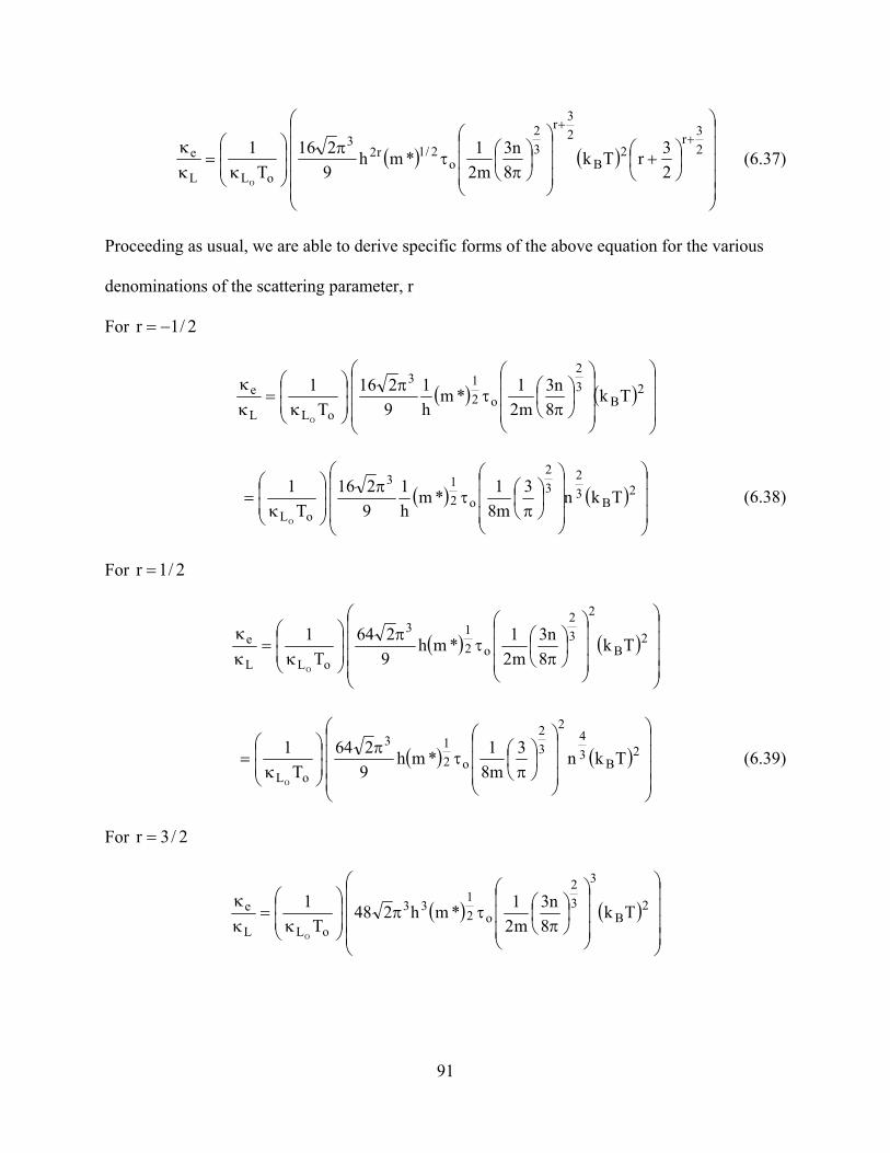
( ) ( )⎟⎟⎟⎟⎟
⎠
⎞
⎜⎜⎜⎜⎜
⎝
⎛
⎟⎠⎞
⎜⎝⎛ +
⎟⎟⎟
⎠
⎞
⎜⎜⎜
⎝
⎛⎟⎠⎞
⎜⎝⎛π
τπ
⎟⎟⎠
⎞⎜⎜⎝
⎛
κ=
κκ +
+
23r
2B
23r
32
o2/1r2
3
oLL
e23rTk
8n3
m21*mh
9216
T1
O
(6.37)
Proceeding as usual, we are able to derive specific forms of the above equation for the various
denominations of the scattering parameter, r
For 2/1r −=
( ) ( )⎟⎟⎟
⎠
⎞
⎜⎜⎜
⎝
⎛
⎟⎟⎟
⎠
⎞
⎜⎜⎜
⎝
⎛⎟⎠⎞
⎜⎝⎛π
τπ
⎟⎟⎠
⎞⎜⎜⎝
⎛
κ=
κκ 2
B32
o213
oLL
e Tk8
n3m21*m
h1
9216
T1
O
( ) ( )⎟⎟⎟
⎠
⎞
⎜⎜⎜
⎝
⎛
⎟⎟⎟
⎠
⎞
⎜⎜⎜
⎝
⎛⎟⎠⎞
⎜⎝⎛π
τπ
⎟⎟⎠
⎞⎜⎜⎝
⎛
κ= 2
B32
32
o213
oLTkn3
m81*m
h1
9216
T1
O
(6.38)
For 2/1r =
( ) ( )⎟⎟⎟⎟
⎠
⎞
⎜⎜⎜⎜
⎝
⎛
⎟⎟⎟
⎠
⎞
⎜⎜⎜
⎝
⎛⎟⎠⎞
⎜⎝⎛π
τπ
⎟⎟⎠
⎞⎜⎜⎝
⎛
κ=
κκ 2
B
2
32
o213
oLL
e Tk8
n3m21*mh
9264
T1
O
( ) ( )⎟⎟⎟⎟
⎠
⎞
⎜⎜⎜⎜
⎝
⎛
⎟⎟⎟
⎠
⎞
⎜⎜⎜
⎝
⎛⎟⎠⎞
⎜⎝⎛π
τπ
⎟⎟⎠
⎞⎜⎜⎝
⎛
κ= 2
B34
2
32
o213
oLTkn3
m81*mh
9264
T1
O
(6.39)
For 2/3r =
( ) ( )⎟⎟⎟⎟
⎠
⎞
⎜⎜⎜⎜
⎝
⎛
⎟⎟⎟
⎠
⎞
⎜⎜⎜
⎝
⎛⎟⎠⎞
⎜⎝⎛π
τπ⎟⎟⎠
⎞⎜⎜⎝
⎛
κ=
κκ 2
B
3
32
o21
33
oLL
e Tk8
n3m21*mh248
T1
O
91

( ) ( )⎟⎟⎟⎟
⎠
⎞
⎜⎜⎜⎜
⎝
⎛
⎟⎟⎟
⎠
⎞
⎜⎜⎜
⎝
⎛⎟⎠⎞
⎜⎝⎛π
τπ⎟⎟⎠
⎞⎜⎜⎝
⎛
κ= 2
B2
3
32
o21
33
oLTkn3
m81*mh248
T1
O
(6.40)
Now the algebra in the above Eqs., (6.37), (6.38), (6.39) and (6.40), can still be worked
out further and the terms better rearranged, and thus the equations are finally written as follows
( ) 2
3r23
3r2
23r2
2Bo
2/1r23
r26
3r23
r3
oLL
e23rTn
m
k*mh
3
2T
1
O
++
+
−
−
−
⎟⎠⎞
⎜⎝⎛ +
τπ⎟
⎟⎠
⎞⎜⎜⎝
⎛
κ=
κκ
(6.41)
For 2/1r −=
( ) 2322
Bo2/13
1
4
723
oLL
e Tnhm
k*m3
2T
1
O
τ⎟⎟⎠
⎞⎜⎜⎝
⎛ π⎟⎟⎠
⎞⎜⎜⎝
⎛
κ=
κκ (6.42)
For 2/1r =
( ) 23
4
2
2Bo
2/131
2
521
oLL
e Tnm
k*mh3
2T
1
O
τ⎟⎟⎠
⎞⎜⎜⎝
⎛ π⎟⎟⎠
⎞⎜⎜⎝
⎛
κ=
κκ
(6.43)
For 2/3r =
( ) 22
3
2Bo
2/13
29
3
oLL
e Tnm
k*mh
2
3T
1
O
τπ⎟⎟⎠
⎞⎜⎜⎝
⎛
κ=
κκ
(6.44)
92

Chapter 7
Correlations of the Reduced Fermi Energy and the
Thermoelectric Figure of Merit as Functions of the
Free Charge Carrier Concentration and the Absolute
Temperature
At this point, it is naturally appropriate to derive theoretical relationships expressing the
dimensionless thermoelectric figure of merit, ZT, as a function of the concentration of free
charge carriers, n, and the absolute temperature, T. We will carry out this new investigation, as
usual, first for nondegenerate, and then for degenerate, semiconductors.
For nondegenerate semiconductors, ZT is given by Eq. (5.11), which we will rewrite as
follows
25r2
25r
ZT2
++η−+
η= (7.1)
From Eq. (6.19), we can derive the following equation for the reduced Fermi energy, η, for a
nondegenerate semiconductor
⎟⎟⎟
⎠
⎞
⎜⎜⎜
⎝
⎛⎟⎠⎞
⎜⎝⎛ π
=η−
23
2B
hTk*m2
2nln (7.2)
or
93

⎟⎟⎟⎟
⎠
⎞
⎜⎜⎜⎜
⎝
⎛
⎟⎟⎠
⎞⎜⎜⎝
⎛
π=η
23
B
2
Tk*m2h
2nln (7.3)
or
( ) ⎟
⎟⎟
⎠
⎞
⎜⎜⎜
⎝
⎛
π=η
23
B
3
23
k*m2
h21
T
nln (7.4)
or
( ) ⎟
⎟⎟
⎠
⎞
⎜⎜⎜
⎝
⎛
π+
⎟⎟⎟
⎠
⎞
⎜⎜⎜
⎝
⎛=η
23
B
3
23
k*m22
hln
T
nln (7.5)
The second term between parentheses on the right-hand side of Eq. (7.5) can be considered
another constant of nature, since its value depends on Planck’s constant, Boltzmann’s constant
and the effective mass of the electron.. The latter can be approximately estimated on the basis of
the mass of the free electron, m, multiplied by a factor which may be provisionally considered
somewhat greater than 1. In carrying out our calculation of the aforementioned term, we have
roughly assumed that factor to be 1.5. That is, undoubtedly, not a bad assumption, since we are
merely trying to find out the order of magnitude value of that term. Our calculations run as
follows
( )
( )
( )23
322
23
54
1023
23
B
3Km10127.1
1038066.110953.95.122
1062618.6
k*m22
hA −
−
−×=
××××π
×=
π=
(7.6)
With reference to Eq. (7.6) above, we have assumed that m5.1*m = , where m is the
electronic free mass. If the effective mass, m*, of the nondegenerate semiconducting material,
94

under investigation, happens to be known and to conform to the relation, fm*m = , where
, then Eq. (7.6) should be modified as follows 5.1f ≠
2223
23
m5.1fm 10f5.1127.1
f5.1AA −×⎟
⎠⎞
⎜⎝⎛=⎟
⎠⎞
⎜⎝⎛= (7.7)
Eq. (7.7) should then be used instead of Eq. (7.6) for all calculations of n as a function of T and
η, and eventually also ZT and S, whenever 5.1f ≠ .
Since Eqs. (7.2) to (7.5) are logarithmic, and since η is dimensionless, therefore, the
argument of the logarithm must also be dimensionless. Thus, Eq. (7.5) should better be written
as follows
⎟⎟⎟
⎠
⎞
⎜⎜⎜
⎝
⎛=η
23
T
nAln (7.8)
Trying to express ZT as a function of n and T, through the substitution of Eq. (7.8) into Eq. (7.1),
will eventually prove not practical or successful. We will end up obtaining a quadratic, or
second degree, polynomial, where the main variable is the logarithm of n, T and a constant. The
best bet would then be to try to optimize the dimensionless thermoelectric figure of merit with
respect to either of the two variables, n or T, while maintaining the other constant. Doing so, we
proceed as follows, operating on Eq. (7.1)
( ) 0n
2n
25r
2n
ZT=
∂η∂
−∂η∂
+
η=
∂∂ (7.9)
or
1
25r=
+
η (7.10)
which yields
95
25r +=η (7.11)
For 2/1r −=
225r =+=η (7.12)
For 2/1r =
325r =+=η (7.13)
For 2/3r =
425r =+=η (7.14)
The correlation between ZT and both n and T could generally be as follows, according to Eq.
(7.1)
25r
TnAln(2
25r
TnAln
ZT 2/3
2/3++⎟
⎠⎞
⎜⎝⎛−
+
⎟⎠⎞
⎜⎝⎛
= (7.15)
Looking now more carefully into Eqs. (7.9) to (7.11), and the values of η that resulted
therefrom, namely, Eqs. (7.12) to (7.14), we immediately realize that these results are
misleading. The values of the reduced Fermi energy, η, for nondegenerate semiconductors, must
always be negative, whereas for degenerate semiconductors, these values are always positive.
These are the rules established by H.J. Goldsmid73, and we are not going to violate or disregard
them in this dissertation. The veracity of these rules can be immediately established by means of
the following example: We need to find the reduced Fermi energy for a nondegenerate
semiconductor for which carriers cm-3 and 18101×=n KT 1000= . Substituting the value of A
given by Eq. (7.6) into Eq. (7.8) yields
96

( )
637.51000
1010110127.1ln 2/3
61822 −=⎟
⎟⎠
⎞⎜⎜⎝
⎛ ××××=η −
We thus must now move in a different direction in this analysis. Instead of attempting to
maximize or optimize ZT, we will take the initiative to find out what happens to ZT when η
acquires the maximum or the minimum acceptable values, respectively. Invoking Eq. (7.1), we
thus obtain
For 2−=η
( ) ( )25r22
25r
2ZT2
++−−+
−= (7.16)
or
25r4
25r
4ZT ++++
= (7.17)
For 2/1r −=
8242ZT =++= (7.18)
For 2/1r =
333.83434ZT =++= (7.19)
For 2/3r =
9441ZT =++= (7.20)
For 4−=η
( ) ( )25r42
25r
4ZT2
++−−+
−= (7.21)
or
97

25r8
25r
16ZT ++++
= (7.22)
For 2/1r −=
18288ZT =++= (7.23)
For 2/1r =
333.16383
16ZT =++= (7.24)
For 2/3r =
16484ZT =++= (7.25)
The above results, as given by Eqs. (7.18) to (7.20), indicate that ZT values of from 8 to 9
are achievable for nondegenerate semiconductors for which the reduced Fermi energy equals -2.
Subsequent results, yielded by Eqs. (7.23) to (7.25), likewise show that ZT values ranging from
16 to 18 are attainable for nondegenerate semiconductors, for which the reduced Fermi energy
equals -4. These new results, developments or conclusions should have come as a totally
unexpected surprise to us. However, there is actually no big mystery about them. They came
about as a natural consequence of substituting the minimum or maximum values of the reduced
Fermi energy, that a nondegenerate semiconductor is allowed to have in order to perform
satisfactorily, into Eq. (7.1). Nevertheless, something very important has already happened, at
least theoretically and motivationally. The above new developments show that a dimensionless
thermoelectric figure of merit, ZT, of much greater value than the current experimental one of
about 1.5, should be achieved in practice. Nonetheless, believing that ZT values as high as 8 to
18 are achievable or possible does not necessarily assure or guarantee that such a spectacular
development will come about in real life. That will depend, more than anything else, on one
issue only, and that is whether a semiconducting material can be found whose thermoelectric
98

power, or Seebeck coefficient, conforms to the data given in Table (1). This is where the real
issue or challenge in thermoelectrics lies. When we constructed that Table, we started by
selecting certain values for ZT, from 1 to 100, and then calculated the corresponding Seebeck
coefficients through multiplying ZT by the Lorenz number and then getting the square root of the
product. What happens in real life is exactly the opposite. It is the value of the measured
Seebeck coefficient of the material we select that determines how much ZT will be, and here is
where the crux in thermoelectrics lies. We can now use Table (1) to find, either directly or by
interpolation, the values of the Seebeck coefficient that a nondegenerate semiconducting material
must have in order to produce ZT values in the range from 8 to 18, as indicated above. We are
going to address this issue once more very soon. For the time being, however, let us pause here
and proceed to investigate the degenerate case.
For degenerate semiconductors, ZT is given by Eq. (5.17), which we will rewrite as
follows
2
22 123r
3ZT
η⎟⎠⎞
⎜⎝⎛ +
π= (7.26)
Now, by definition, Tk/E BF=η , and invoking Eq. (5.22), gives
⎟⎠⎞
⎜⎝⎛ +⎟
⎠⎞
⎜⎝⎛π
=η23r
Tk1
8n3
m2h
B
32
2 (7.27)
where
VN
n e= (7.28)
which is the number of free charge carriers, per unit volume, also known as the free charge
carrier concentration. Eq. (7.27) can be worked further, which yields
99

⎟⎠⎞
⎜⎝⎛ +⎟
⎠⎞
⎜⎝⎛π
=η23r
Tn3
mk8h 3
2
32
B
2 (7.29)
From the very beginning of this investigation, when we constructed Table (1), we were
able to infer, or conclude, that the Seebeck coefficient, S, for degenerate semiconductors, is not a
function of the electronic scattering parameter or index, r. That has happened, because the
Lorenz number, L, for degenerate semiconductors is not a function of r. Consequently, the
dimensionless thermoelectric figure of merit, ZT, also is not a function of r. These results or
conclusions can be inferred from either Eq. (5.6) or Eq. (5.25).
When we constructed Table (2), earlier in this dissertation, we found that the values of
the reduced Fermi energy, η, for degenerate semiconductors were related to one another in the
ratio of 1:2:3 corresponding to , and , respectively. This evidently
demonstrates a linear dependency of η on
2/1−=r 2/1 2/3
⎟⎠⎞
⎜⎝⎛ +
23r . This is also proven, if we factor η out of Eq.
(5.17)
⎟⎠⎞
⎜⎝⎛ +
π=η
23r
ZT3
This means that both S and ZT are not functions of r for degenerate semiconductors.
Substituting now Eq. (7.29) into Eq. (7.26), gives rise to
34
2342
2B
2
n
T3h
mk83
ZT ⎟⎠⎞
⎜⎝⎛ π⎟
⎠⎞
⎜⎝⎛π
= (7.30)
or
34
2
n
TBZT = (7.31)
100

where
2422223
42
2B
2Km1018372819.0
A1
33hmk8
3B −−×=⎟
⎠⎞
⎜⎝⎛π
=⎟⎠⎞
⎜⎝⎛ π⎟
⎠⎞
⎜⎝⎛π
= (7.32)
where the constant , and the constant, A, has been defined and calculated according
to Eq. (6.11).
22 A3/B π=
For degenerate semiconductors, regardless of r
34
2
n
TBZT = (7.33)
Looking now into the above Eqs., (7.30) to (7.33), we realize that we have already
succeeded in establishing a general relationship between ZT and both n and T, which is Eq.
(7.31). We may thus consider this part of our investigation concluded.
At this point in our research, it is probably appropriate to focus our attention and efforts
on the dimensionless thermoelectric figure of merit, ZT, for both nondegenerate and degenerate
semiconductors, in order to find out the ZT values that can possibly be achieved, at least
theoretically. We will try to determine the limits that could eventually be set or placed on those
possible ZT values. The aforementioned limits could originate from the values of the free charge
carrier concentration or temperature, or a combination of both, required to create certain allowed,
predetermined or preferred reduced Fermi energy values which are fundamentally conducive to
attaining those possible ZT values. Although less likely, additional constraints could still be
placed on the possible ZT values, if we set our goal, for example, at a ZT value equal, or close,
to 100. The Seebeck coefficient required in that case could be too demanding, or difficult to
achieve, with any material whatsoever.
Part of the research work referred to above has already been carried out earlier in relation
101

to nondegenerate semiconductors. We have been able to verify, for example, that when the
scattering parameter , the magnitude of ZT becomes 8 and 18, for 2/1r −= 2−=η and 4− ,
respectively. Looking now into Table (2), we notice that we could still push η down to a value
which is slightly below the minimum allowed value, or limit, of 4− , i.e., , and thus get
. This ZT value is the maximum we can achieve with any nondegenerate
semiconducting material. If we still choose to ignore this result and look instead into Table (1),
as an alternative, we could argue as follows: We could base our criterion on the Seebeck
coefficient and assume that is attainable. This could be true for a few
semiconductors, not at room temperature of course, but at higher temperatures. Looking into
Table (1) for nondegenerate semiconductors, for which
32.4−
20=ZT
1VK1000S −μ=
2/1r −= and , we
interpolate a corresponding value of
1VK1000S −μ=
6.67ZT = . Looking back into Table (2), we see that such a
ZT value corresponds to 62.9−=η , which is far below the minimum allowed value, or limit, of
, as established by Goldsmid. Thus, 4− 6.67ZT = cannot be achieved for nondegenerate
semiconductors, regardless of the value of r. Therefore, we end up reconfirming our original
conclusion which runs as follows:
For nondegenerate semiconductors
( ) 20ZT MAX = (7.34)
and is most appropriate for . The above result is an important finding of this
dissertation.
2/1r −=
Let us continue our analysis of nondegenerate semiconductors in order to help us
construct new tables that give the free charge carrier concentration, or doping level, necessary to
achieve certain predetermined values of ZT for certain constant temperature values. Those
constant temperatures will be 300, 500, 750 and 1000K. We will do all the numerical
102

calculations with the help of Eqs. (7.1) to (7.8).
We will thus proceed as follows: From Eq. (7.8), we deduce
( ) 2/3TnAlneln =η (7.35)
therefore
2/3TnAe =η
or (7.36)
2/3TAenη
=
Considering, for example, the case in which 2−=η , we thus proceed as follows
For : K300T = ( ) 18622
2/321024.610
10127.1300en ×=××
= −−
− carriers cm-3
For : K500T = ( ) 19622
2/321034.110
10127.1500en ×=××
= −−
− carriers cm-3
For : K750T = ( ) 19622
2/321047.210
10127.1750en ×=××
= −−
− carriers cm-3
For : K1000T =( ) 196
22
2/321080.310
10127.11000
×=××
= −−
−en carriers cm-3
The free charge carrier concentration, n, has thus generally been calculated for 2−=η ,
, , , , , and 32.2− 47.2− 48.2− 3− 4− 32.4− 5− . All of these results are summarized and
presented in Tables (7), (8) and (9), and are related to nondegenerate semiconductors for which
, and , respectively. In order to render the aforementioned tables still more
practical and useful, the corresponding ZT and S values have also been included at the bottom of
each one of them.
2/1r −= 2/1 2/3
103
All the calculated data referred to above, as summarized in Tables (7), (8) and (9),
conclude our investigation in relation to nondegenerate semiconductors, and serve to
demonstrate the following:
(1) When using nondegenerate semiconductors for thermoelectric energy conversion, operating
in the temperature range of 300K to 1000K, and maintaining the reduced Fermi energy
approximately in the range from to 2− 4− and the free charge carrier concentration within the
limits of to carriers cm-3, a dimensionless thermoelectric figure of merit,
ZT, of from 8 to 20 can be achieved, depending on the value of the scattering index, r.
171013.6 × 191047.2 ×
(2) In order for the above results, specifically ZT, to be realized, a minimum Seebeck coefficient
must be generated or maintained by the semiconductors, as indicated in these tables.
(3) If the operating temperature can be maintained in the range from 500K to 1000K the above
requirement for the Seebeck coefficient, S, should prove less difficult (although still not
guaranteed).
(4) The material that places the least demand on S is that for which 2/1r −= , which is the
material in which acoustic-mode lattice scattering or alloy scattering predominates. Therefore,
such a material should be preferred or selected for that purpose.
(5) The values of n for and K1000T = 2−=η and 32.2− are and
carriers cm-3, respectively. These n values are untenable and represent cases of reductio ad
absurdum, since the uppermost value, or limit, of n for nondegenerate semiconductors is
carriers cm-3. Therefore, these cases are unacceptable and must be disregarded, since
they relate to degenerate semiconductors.
191080.3 × 191076.2 ×
19105.2 ×
We now must go back and carry out a more thorough and detailed analysis of degenerate
semiconductors. We will specifically concentrate our effort on Eq. (7.33) in order to find out the
104

ZT values that can possibly be achieved for certain values of the free charge carrier
concentration, n, and the temperature, T. Or better still, we can calculate the values of n, for
certain predetermined values of T, required to attain specific predetermined integral values of
ZT. The latter could be taken directly from Tables (1) or (2). Those predetermined values of T
could be set at 300K, 500K, 750K and 1000K. We thus select beforehand the values of both ZT
and T, and end up obtaining the value of n, using Eq. (7.33). Of course, there are constraints
placed on n. Its value must be higher than carriers cm-3 and must not exceed
carriers cm-3. The latter is inconsequential, since we are more concerned or interested in keeping
n as low as possible, i.e., only slightly above carriers cm-3, in order to ensure that we
will get the maximum ZT possible for a certain constant, or predetermined, temperature T, while
assuring that the material still remains degenerate.
19105.2 × 20105×
19105.2 ×
Investigating degenerate semiconductors, we look into Table (1) or Table (2) and use
those ZT values, set forth in the left hand column thereof, as the input to our analysis. We will
use the same standard set of 300K, 500K, 750K and 1000K as our preselected temperatures, as
we did with the nondegenerate semiconductors. We will now invoke Eq. (7.33) and substitute
the aforementioned two inputs, i.e., the dimensionless thermoelectric figure of merit, ZT, and the
temperature, T, into that equation. We will thus finally obtain the free charge carrier
concentration, n. The so-obtained value of n should then be examined as to whether it falls
within the range: carriers cm-3. If it doesn’t, then the ZT value that we
used as an input must be rejected, since that means that that ZT value cannot be realized in
practice at the preselected temperature, T.
2019 105n105.2 ×<<×
We will thus have to rewrite Eq. (7.33) as follows, in order to put it into a more
appropriate form
105
ZT
BTn2
34
= (7.37)
or
43
2
ZTBTn ⎟
⎟⎠
⎞⎜⎜⎝
⎛= (7.38)
We may now proceed to investigate degenerate semiconductors regardless of the value of
r, since their ZT does not depend on r.
Using, therefore, Eq. (7.38) enables us to construct Table (10), which gives values of the
free charge carrier concentration, n, as a function of the dimensionless thermoelectric figure of
merit, ZT, and the temperature, T, for degenerate semiconductors.
Examining now Tables (7), (8) and (9) as well as Table (10) enables us to draw some
very important conclusions concerning the magnitude of ZT that is to be expected from
nondegenerate and degenerate semiconductors that constitute the p-type and n-type
thermoelements or branches of devices for direct thermoelectric energy conversion.
Let us concentrate first on Tables (7), (8) and (9), related to nondegenerate
semiconductors, for which , and , respectively. For 2/1r −= 2/1 2/3 2/1r −= , which refers to
Table (7), we notice that when 2−=η and K1000T = , the concentration of free charge carriers
carriers cm-3, which is much higher than the well known limit for nondegenerate
semiconductors, carriers cm-3. Referring to Table (7), this means that in order for
that semiconductor to bring about ZT and S values of 8 and 344μVK-1, respectively, the material
must actually be a degenerate semiconductor. This violates the original assumption of this
analysis that the material is a nondegenerate semiconductor. This kind of contradiction is called:
“reductio ad absurdum,” that is, “reduction to the absurd.” All that leads to the conclusion that
191080.3n ×=
19105.2n ×=
106

the ZT and S values of 8 and 344μVK-1, respectively, cannot be realized in practice when
T=1000K and 2−=η . The aforementioned ZT and S values are, however, possible for lower
temperatures. In the latter case, that means that as long as the n and T values match, or
correspond to each other, as given in the table, and as long as the material is capable of
generating an S value as indicated, then the ZT value given in the table is guaranteed, or
automatically achieved. The foregoing analysis applies to all three tables. That means that the
only ZT value that is not achievable is that for which 2−=η and T=1000K, regardless of the
value of r. Comparing the three Tables, (7), (8) and (9), we notice that the highest ZT value for a
nondegenerate semiconductor, i.e., 24.5, is achieved through a material for which ,
which again refers to Table (7). In that case,
2/1r −=
5−=η and the material must be capable of
generating a thermoelectric power or Seebeck coefficient, S=602μVK-1. If the material fails to
generate or bring about a Seebeck coefficient of the aforementioned magnitude, then the
foregoing highest magnitude of ZT will not be achieved. And that is because both quantities, ZT
and S, are tied-up together through Eq. (5.6).
Looking now into Table (2), and referring once more to a nondegenerate semiconductor
for which , we infer that by reducing the value of the reduced Fermi energy, η, from
to , , , ,
2/1r −=
5− 75.5− 94.6− 00.8− 95.8− 83.9− , 65.10− , 42.11− and 14.12− , we could get ZT
values of 30, 40, 50, 60, 70, 80, 90 and 100, respectively, as well as S values of 666, 769, 860,
942, 1018, 1088, 1154 and 1217 μVK-1, respectively. So we may initially fall under the
influence of unbridled enthusiasm and think that the sky is only the limit as to how far we can go
in thermoelectrics. Unfortunately, this is not so. While dealing with nondegenerate
semiconductors, we should not lose sight of the fact that the reduced Fermi energy, η, values are
all negative and start pointing downwards from the edge of the conduction band or upwards from
107
the edge of the valence band. Furthermore, it is necessary that 0<<η , i.e., that the Fermi level
lies within the forbidden band gap well away from the appropriate band edge and also that the
Fermi level should be much further from the opposite band edge, if minority carriers are to be
neglected or avoided. The foregoing imposes a powerful constraint upon how much can we
lower the reduced Fermi energy, η. The following rule is thus established: We should lower η
as much as we can so that 4−<η , but we cannot go below the middle of the forbidden energy
band gap, because the minority carriers from the opposite band edge will start adversely
affecting the Seebeck coefficient, S, which will lead to a deterioration of the thermoelectric
performance of the semiconductor.
A simple rule or relationship that could be used to calculate the minimum value of the
reduced Fermi energy, η, for a nondegenerate semiconductor, for which the forbidden energy
band gap, Eg, is known, is therefore the following: A certain confusion that may ensue due to the
fact that Eg is a positive, while η is a negative, quantity, can be removed by neglecting the
negative sign of η. In this case, we will actually be calculating the maximum absolute value of
the reduced Fermi energy, and then we will simply apply the negative sign to it, and thus
everything will be restored back to normal. Thus the relationship is expressed as follows
2
ETkE g
BF =η= (7.39)
or
Tk2
E
B
g=η (7.40)
or
Tk2
E
B
g−=η (7.41)
108

In order to avoid any possible confusion related to their future use, Eqs. (7.40) and (7.41)
should be designated as referring to the maximum absolute value, and minimum value, of the
reduced Fermi energy, respectively. We thus rewrite them as follows
Tk2
E
B
gMAX =η (7.42)
or
Tk2
E
B
gMIN −=η (7.43)
In order to be able to use Eqs. (7.42) and (7.43), both the energy band-structure diagram
and the forbidden energy band gap, Eg, for the specific material under investigation, must be
known or available. If that is not so, then it will be impossible for us to know how far we can go
in lowering the reduced Fermi energy, η, in order to get the best possible values of S and ZT. In
that case then, the only alternative we would have would be to carry out experimental research
work on the material in question. Let us now work out some numerical calculations using Eqs.
(7.42) and (7.43), so that we may get the feel of what kind of results can be expected from them.
For a semiconductor having, for example, a forbidden energy band gap, eV, and
operating at a temperature, T=1000K, we obtain
78.0Eg =
53.410001038066.12
1060219.178.0Tk2
E23
19
B
gMAX =
×××
××==η
−
−
or
53.4MIN −=η
The above result for ηmin seems reasonable, and for a semiconductor for which yields a
dimensionless thermoelectric figure of merit, ZT=21.32. Continuing the above calculation for
the operating temperatures of 750K, 500K and 300K, we obtain additional results which, along
2/1r −=
109

with the foregoing one for T=1000K, are presented as shown in Table (11).
A study of the foregoing results indicates that the values of the minimum reduced Fermi
energy, ηmin, of and, to a lesser extent, 53.4− 03.6− corresponding to 1000K and 750K,
respectively, can be considered tentatively approved or acceptable, whereas those corresponding
to 500K and 300K, respectively, i.e., 05.9− and 9.15− , should be regarded as unreliable and
suspicious. The reason they acquired such huge magnitudes is purely mathematical and
emanates from Eq. (7.43), but there is no physical evidence to support it or back it up.
Therefore, the latter two values are rejected. It is extremely unlikely to be able to manufacture,
or come across, a semiconducting or thermoelectric material that would generate or bring about
Seebeck coefficients, S, of 951 and 1470 μVK-1, and figures of merit, ZT, of 61 and 146 at such
relatively low temperatures as 500K and 300K, respectively. Since, in this dissertation, we are
essentially more interested in thermoelectric power generation than in thermoelectric
refrigeration and/or thermoelectric heat pumping, we are naturally more focused on investigating
the higher temperature range up to 1000K, since that would lead to the highest possible Carnot
engine energy conversion efficiency, according to the second law of thermodynamics. Operating
our power generating thermoelectric device at such low temperatures as 500K or 300K,
considered hot junction, or hot end, temperatures, doesn’t make sense and could eventually be
conducive to a very low or even zero Carnot engine efficiency, and we don’t want that.
In the above investigation or analysis, we have used Eq. (5.11) to calculate ZT from
values of η determined on the basis of the width of the forbidden energy band gap, Eg, i.e., Eqs.
(7.42) and (7.43). We then used Eq. (5.6) to obtain the corresponding values of the Seebeck
coefficient, S. When doing that, we should always make sure that Eq. (5.6) is valid. As long as
the lattice thermal conductivity has been reduced to its absolute minimum value, through mass
110
and volume fluctuation scattering, also known as alloy scattering, or through any other means,
and even if the alloy or material is lightly doped, or even undoped, and even if the temperature is
at least not below room temperature, then Eq. (5.6) should still be considered reliable and
standing on a firm foundation. For that purpose, Eqs. (6.32), (6.33) and (6.34) as well as Eqs.
(6.42), (6.43) and (6.44) for nondegenerate and degenerate semiconductors, respectively, should
be used whenever the validity of Eq. (5.6) needs to be verified or checked. In this context, a
rather suspicious situation has come about in Table (11), where we have the T and n combination
of 300K and carriers cm-3, which certainly is untenable. Another situation, which is
still similar but less serious, is given by T=500K and carriers cm-3.
131029.1 ×
161016.1 ×=n
Comparing now Tables (7), (8) and (9) with each other, we notice that, e.g., for 5−=η ,
the highest ZT value is given by Table (7) and the lowest is given by Table (9), i.e., 24.5 and
20.25, respectively. We also notice that the lowest value for the Seebeck coefficient, S, is given
by Table (7) and the highest is given by Table (9), i.e., 602 and 774 μVK-1, respectively. Thus,
of all three tables, Table (7) is the one that yields the highest ZT value possible and it also is the
one that requires the lowest value for the Seebeck coefficient, S. This leads to the conclusion
that, when dealing with nondegenerate semiconductors in general, we should select one for
which , that is, one in which either acoustic-mode lattice scattering or alloy scattering is
predominant. The lower the demand on the Seebeck coefficient, the more likely it is that such a
demand will be realized, or met, in practice. That is why, should we decide to use a
nondegenerate semiconductor for direct thermoelectric energy conversion, we should always
choose one for which .
2/1r −=
2/1r −=
We examine now Table (10) related to degenerate semiconductors. We notice that for
T=300K, only the ZT values of 1 and 2 are possible. The rest of the ZT values, from 3 to 100,
111

represent cases of “reductio ad absurdum,” since the free charge carrier concentration, n, has to
remain below carriers cm-3, i.e., the material must actually be nondegenerate. This
violates the original assumption that the material is a degenerate semiconductor. Thus those ZT
values from 3 to 100 cannot be achieved or realized in practice. For T=500K, only the ZT values
from 1 to 5 are possible, the remaining ZT values, from 10 to 100, are cases of reductio ad
absurdum, and thus they cannot be realized in practice. For T=750K, only the ZT values from 1
to 10 are possible, the remaining ones, from 20 to 100, are impossible to realize in practice. For
T=1000K, only the ZT values from 1 to 20 are possible, the remaining ones, from 30 to 100, are
impossible to realize in practice. For a degenerate semiconductor, again maintaining T=1000K,
if we lower n down to carriers cm-3 and use Eq. (7.37), we obtain ZT=23.85 which is
almost identical with, or equal to, the highest ZT value obtained with a nondegenerate
semiconductor for which and
19105.2 ×
19106.2 ×
2/1r −= 5−=η (Table (7)).
The foregoing observations, which can be easily inferred from Eq. (7.33), serve to bring
into sharp focus two of the most important characteristics of degenerate semiconductors:
(1) The higher the temperature, the better is the thermoelectric performance.
(2) The higher the level of doping, the lower is the thermoelectric performance.
It is now time to proceed with the construction of Table (12), which is the same as Table
(1) except that the Seebeck coefficient, S, for degenerate semiconductors, appears to depend on
the scattering parameter, r, as can be seen from Eq. (5.15). Table (12) will thus contain three
different values, for degenerate semiconductors, and three different values, for nondegenerate
semiconductors, of the Seebeck coefficient, or thermoelectric power, S, for each predetermined
ZT value. We will thus start calculating the values of the Seebeck coefficient, S, from the values
of the reduced Fermi energy, η, corresponding to predetermined values of the dimensionless
112

thermoelectric figure of merit, ZT, and appropriate values of the scattering parameter, r, for both
degenerate and nondegenerate semiconductors, as presented in Table (2). To do that, we will
have to rely on Eqs. (5.8) and (5.15) for nondegenerate and degenerate semiconductors,
respectively. Three sample calculations for each of degenerate and nondegenerate
semiconductors are shown below.
Degenerate Semiconductors:
2/1r −=
16
19
232B
2VK156
814.110
1060219.11038066.1
31
ek
3S,814.1,1ZT −
−
−μ=
×
×π=
ηπ
==η=
2/1r =
16
19
232B
2VK156
628.310
1060219.11038066.1
321
ek
32S,628.3,1ZT −
−
−μ=
×
×π=
ηπ
==η=
2/3r =
16
19
232B
2VK156
441.510
1060219.11038066.11
ek
33S,441.5,1ZT −
−
−μ=
×
×π=
ηπ
==η=
Nondegenerate Semiconductors:
2/1r −=
119
623B VK385
1060219.1101038066.147.4
25r
ekS,47.2,10ZT −
−
−μ=
×
×××−=⎥
⎦
⎤⎢⎣
⎡⎟⎠⎞
⎜⎝⎛ +−η=−=η=
2/1r =
( ) 119
623B VK472
1060219.1101038066.148.5348.2
ek
S,48.2,10ZT −−
−μ=
×
×××−=−−=−=η=
2/3r =
( ) 119
623B VK545
1060219.1101038066.132.6432.2
ek
S,32.2,10ZT −−
−μ=
×
×××−=−−=−=η=
113
In the foregoing six sample calculations for degenerate and nondegenerate
semiconductors, as well as in this entire dissertation, we have ignored any negative sign that S
might have, or acquire, i.e., we have reported only the absolute values of the Seebeck coefficient.
The plus-or-minus signs associated with Eqs. (5.8) and (5.15) are meant to ensure that the sign of
the Seebeck coefficient, S, is negative if the free charge carriers are predominantly electrons and
positive if the free charge carriers are predominantly holes.
Checking first the values of the thermoelectric power, S, as obtained according to the
three sample calculations, given above, for degenerate semiconductors, for , and
, respectively, and ZT=1, we notice that they are all the same, i.e., . Looking
now into the data given in Table (12) for the Seebeck coefficient of degenerate semiconductors
for the entire range of ZT values, from 1 to 100, we perceive that S is independent of r for any
ZT value. This is contrary to what we had thought earlier, that the Seebeck coefficient, S,
depends on r. We were led to that conclusion, initially, because Eq. (5.15) shows a dependency
of S on r. We failed to realize, however, that the reduced Fermi energy, η, also depends on the
scattering parameter, r. So, when the two dependencies, i.e., of S and η on r, are included, or
come to act, together, they cancel out, and S, therefore, becomes independent of r. Furthermore,
Table (1), which gives one single value of S, which is independent of r, for every predetermined
value of ZT, turns out to be correct. The data given in Table (1) are based on Eq. (5.6), through
the use of Eq. (5.25). Calculation of the data given in Table (2) for the reduced Fermi energy, η,
for degenerate semiconductors, has been fundamentally carried out by means of Eq. (5.17), while
substituting , and for the different denominations of the scattering parameter,
which has led to the eventual use of Eqs. (5.18), (5.19) and (5.20). A thorough scrutiny of the η
values for , and reveals that indeed those η values are related to one another
2/1r −= 2/1
2/3 1VK156S −μ=
2/1r −= 2/1 2/3
2/1r −= 2/1 2/3
114

in the ratio of 1:2:3, respectively. This, therefore, proves that the dependency of η on r is the
same as that of S on r, when looking at Eq. (5.15). So we end up having the factor, ( ) , in
the numerator and the factor, ( , in the denominator, of that equation. These two factors
then cancel out and S eventually becomes independent of r for degenerate semiconductors. For
each predetermined ZT value, the S values are substantially identical, with insignificant
numerical differences existing among them. Also there exist some minor and virtually negligible
differences between the data presented in Table (12) and the corresponding ones of Table (1).
2/3r +
)2/3r +
For nondegenerate semiconductors, we had to rely on Eq. (5.8) in order to convert the η
values given in Table (2) into the S values that are presented in Table (12). Once more, the S
data given in Table (12) are almost the same as those shown in Table (1), the differences being
insignificant. The reduced Fermi energy, η, data given in Table (2) were obtained, for each
predetermined ZT value, and the relevant r values, through the use of Eq. (5.11), by solving forty
five algebraic quadratic equations and then obtaining the roots or eigenvalues thereof. Those
eigenvalues that did not have a negative sign were ignored or cancelled, since they represented
cases of reductio ad absurdum, i.e., they stood in violation of the original assumption, that the
semiconductor is nondegenerate and, as such, the reduced Fermi energy must be negative. Those
empty spaces in Table (2) are all due to this kind of situation. There is also another restriction
concerning nondegenerate semiconductors, which we chose not to implement. For
nondegenerate semiconductors, the rule, as given in Table (13), is that 2−<η and preferably
that 4−<η . We did not apply that rule at all, and presented all the η values, that we calculated,
in the table, as long as they were negative. The thermoelectric power or Seebeck coefficient, S,
of nondegenerate semiconductors, as we already know, and as proven through the data set forth
in Tables (1) and (12), is indeed a function of r, for any predetermined ZT value. Having created
115
Tables (1), (2) and (12), has had the effect that all three of them are now standing on a much
firmer foundation. And that applies to both degenerate and nondegenerate semiconductors.
Focusing our attention on all the foregoing data presented in Tables (7)-(11), inclusive, as
well as the lengthy statements and comments made with reference thereto, we are in a position
now to draw several very significant conclusions with respect to how to select semiconducting
materials, both degenerate and nondegenerate, their range of operation and the maximum
performance that can be expected therefrom. Nondegenerate semiconductors are more
appropriate for operation at lower temperatures, whereas degenerate ones are more suited to
operate at higher temperatures. When we refer to lower and higher temperatures, what we have
in mind, of course, is the entire temperature range we are dealing with, from 300K to 1000K.
Generally, semiconductors, whether degenerate or nondegenerate, can still be operated at any
temperature whatsoever, as long as they do not become cases of reductio ad absurdum. As far as
the concentration of free charge carriers, or doping level, n, carriers cm-3, of degenerate
semiconductors is concerned, the lower the doping level, the higher the thermoelectric figure of
merit, ZT, will be. So, for degenerate semiconductors, in general, in order to maximize the
thermoelectric performance, or ZT, we have to do two things simultaneously:
(1) Increase the temperature as much as possible.
(2) Decrease the doping level, or free charge carrier concentration, as much as possible.
We could increase the temperature, T, up to about 1000K, while trying to avoid overdoing it, for
two very important reasons:
(a) The melting point of the material, Tm, may be reached or approached.
(b) The state of the material may change from extrinsic to intrinsic, which normally leads to a
drop in the Seebeck coefficient and a consequent deterioration or decrease of ZT. We should
116
thus increase the temperature way up as much as we can, while avoiding reaching both the
melting and intrinsic temperatures, Tm and Tint. There is no fixed upper temperature limit for
degenerate semiconductors, because that may individually vary from one material to another.
Lowering the doping level, n, of degenerate semiconductors is not going to be an easy task,
because we are already hampered by the fact that their free charge carrier concentration must
always remain higher than carriers cm-3, since otherwise a case of reductio ad
absurdum will be created. The best we can do is maintain n at about 2.6, 2.7 or
carriers cm-3. That is the minimum free charge carrier concentration that a semiconductor can
have while still being classified as degenerate. So, maximizing the temperature, T, along with
minimizing the free charge carrier concentration, n, creates an unbeatable combination that leads
to a vastly superior degenerate semiconducting material with extraordinary thermoelectric figure
of merit, ZT. That, coupled with an enhanced Carnot engine efficiency, due to the higher
operating temperature, leads to maximum overall energy conversion efficiency from heat into
electricity.
19105.2 ×
19108.2 ×
For nondegenerate semiconductors, the situation is entirely different. Eqs. (5.8), (5.9)
and (5.11) do give the Seebeck coefficient, S, the Lorenz number, L, and the figure of merit ZT,
and they are all functions of r. Tables (1) and (12) also reflect this fact. Examining Tables (7),
(8) and (9), and comparing them with each other, we observe that the highest value of the
thermoelectric figure of merit, ZT, for a nondegenerate semiconductor, is 24.5 and is achieved
through a material for which , according to Table (7). Other r denominations, namely
and , yield ZT values of 21.333 and 20.25, respectively. That fact establishes the
superiority of the nondegenerate semiconductor, having
2/1r −=
2/1 2/3
2/1r −= , over the other two, namely
those with and . That fact is further corroborated when we look into Table (1). 2/1r = 2/3r =
117

We then notice that the Seebeck coefficient for any ZT value is lowest when . That
means that for the same ZT value, the Seebeck coefficient is lesser for
2/1r −=
2/1r −= than for 2/1r =
or . That makes the nondegenerate semiconductor for which 2/3r = 2/1r −= our material of
preference among all three nondegenerate semiconductors. The lower the demand or
requirement on the Seebeck coefficient, the more likely it is that such a demand will be met in
practice.
Now we come to study the dimensionless thermoelectric figure of merit, ZT, for
semiconducting materials, in order to draw some final conclusions about it. For nondegenerate
semiconductors, we have already found out that the maximum possible value of the
thermoelectric figure of merit is 5.24ZT = achieved through a material with , 2/1r −= 5−=η
and . Can the foregoing ZT figure be improved or exceeded? Yes, but only if we
could reduce η to a lower value, or, in other words, increase the absolute value of η, i.e.,
1VK602S −μ=
5>η .
We are not so sure that we could do that. Actually, there is a set of 6 criteria in the recent
literature41 on thermoelectrics, the last one of which runs as follows: “For semiconductors, the
best materials should have energy band gaps equal to 10kBT, where T is the operating
temperature of the thermoelectric material.” So, if we combine this criterion with Eq. (7.41), we
have
5Tk2Tk10
Tk2E
B
B
B
gMIN −=−=−=η (7.44)
The above minimum value of η coincides with the lowest η values given in Tables (7), (8) and
(9). In those tables, the decision to make 5−=η was based on pure intuition. The agreement
between these values, actually a single value, and that obtained through Eq. (7.44), above, is a
mere coincidence. Consequently, we are now in a position to finally wrap it up as far as
118
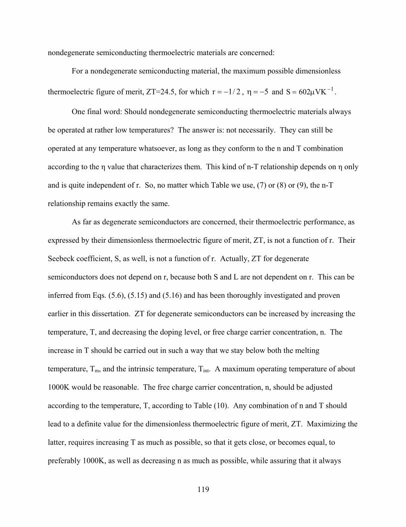
nondegenerate semiconducting thermoelectric materials are concerned:
For a nondegenerate semiconducting material, the maximum possible dimensionless
thermoelectric figure of merit, ZT=24.5, for which 2/1r −= , 5−=η and . 1VK602S −μ=
One final word: Should nondegenerate semiconducting thermoelectric materials always
be operated at rather low temperatures? The answer is: not necessarily. They can still be
operated at any temperature whatsoever, as long as they conform to the n and T combination
according to the η value that characterizes them. This kind of n-T relationship depends on η only
and is quite independent of r. So, no matter which Table we use, (7) or (8) or (9), the n-T
relationship remains exactly the same.
As far as degenerate semiconductors are concerned, their thermoelectric performance, as
expressed by their dimensionless thermoelectric figure of merit, ZT, is not a function of r. Their
Seebeck coefficient, S, as well, is not a function of r. Actually, ZT for degenerate
semiconductors does not depend on r, because both S and L are not dependent on r. This can be
inferred from Eqs. (5.6), (5.15) and (5.16) and has been thoroughly investigated and proven
earlier in this dissertation. ZT for degenerate semiconductors can be increased by increasing the
temperature, T, and decreasing the doping level, or free charge carrier concentration, n. The
increase in T should be carried out in such a way that we stay below both the melting
temperature, Tm, and the intrinsic temperature, Tint. A maximum operating temperature of about
1000K would be reasonable. The free charge carrier concentration, n, should be adjusted
according to the temperature, T, according to Table (10). Any combination of n and T should
lead to a definite value for the dimensionless thermoelectric figure of merit, ZT. Maximizing the
latter, requires increasing T as much as possible, so that it gets close, or becomes equal, to
preferably 1000K, as well as decreasing n as much as possible, while assuring that it always
119

stays above carriers cm-3, and while conforming to Eq. (7.38). That would be our
ideal temperature and doping levels for maximizing the dimensionless thermoelectric figure of
merit, ZT, for degenerate semiconductors.
19105.2 ×
Degenerate semiconductors, therefore, can bring about a maximum thermoelectric figure
of merit, ( ) at 1000K, which is virtually the same as the maximum
thermoelectric figure of merit ( )
85.23ZT MAX =
5.24ZT MAX = , achieved through a nondegenerate
semiconducting material for which the electronic scattering parameter, 2/1r −= , the reduced
Fermi energy, 5−=η and the Seebeck coefficient, . 1VK602S −μ=
Studying now Tables (7), (8) or (9), we notice that for nondegenerate semiconductors,
decreasing the concentration of the free charge carriers, n, i.e., lowering the doping level, while
maintaining the temperature, T, constant, actually increases the Sebeeck coefficient, S. Also,
maintaining the concentration of the free charge carriers, n, constant, while increasing the
temperature, T, for nondegenerate semiconductors, normally increases the Seebeck coefficient,
S. This is corroborated by substituting Eq. (7.2) into Eq. (5.8), and inferring that this will
actually happen. It would then be safe to assume that doing both, i.e., decreasing n, while
increasing T, would tend to increase S much more. This fact, related to nondegenerate
semiconductors, is further supported by Ioffe’s71 formula (21), which is
( )
⎟⎟⎠
⎞⎜⎜⎝
⎛ π+=
nhTk*m22
lnAe
kS 3
2/3BB (7.45)
where the constant according to Goldsmid72. The aforementioned fact has also been
proven experimentally for semiconducting intermetallic compounds, which were substantially in
the undoped state, i.e., having an extremely small free charge carrier concentration, n. The fact
that a nondegenerate semiconducting material will actually experience a large increase in its
2/5rA +=
120

Seebeck coefficient, S, if its temperature is substantially increased, especially when it is also
undoped, i.e., n becomes very small, which has also been corroborated experimentally, is of
paramount significance and should be taken full advantage of. This fact should still not be
considered good enough. The material, furthermore, must already possess a reasonably high
Seebeck coefficient of its own at temperatures equal, or close, to room temperature. Only then,
could we be sure that we are dealing with a really promising and worthwhile thermoelectric
material.
Referring again to nondegenerate semiconductors, we have already mentioned and
applied, quite frequently, the following rules: that the reduced Fermi energy, η, should be at least
less than , and better still that it be less than 2− 4− , i.e., 2−<η or 4−<η , the former rule is
considered acceptable, while the latter is regarded as highly recommended or preferable. Credit
for establishing these rules undoubtedly belongs to Professor H. J. Goldsmid73. In the course of
our work on this dissertation, we have pushed those rules one step further by stipulating that
54 −≥η>− . This is the new rule for nondegenerate semiconductors, which is simultaneously
conducive to achieving the maximum possible ZT value of 24.5. The aforementioned statements
are also presented in a new table, namely, Table (13), for easy reference.
121

TABLE 7. Values of the free charge carrier concentration, n, carriers cm-3, as a function of the temperature, T, K,
and the reduced Fermi energy, η, along with the corresponding values of the dimensionless thermoelectric figure of
merit, ZT, and the Seebeck coefficient, S, μVK-1, for nondegenerate semiconductors for which . 2/1r −=
-2 -2.47 -4 -4.32 -56.24x10¹⁸ 3.90x10¹⁸ 8.44x10¹⁷ 6.13x10¹⁷ 3.11x10¹⁷
1.34x10¹⁹ 8.39x10¹⁸ 1.82x10¹⁸ 1.32x10¹⁸ 6.68x10¹⁷
2.47x10¹⁹ 1.54x10¹⁹ 3.34x10¹⁸ 2.42x10¹⁸ 1.23x10¹⁸
3.80x10¹⁹ 2.37x10¹⁹ 5.14x10¹⁸ 3.73x10¹⁸ 1.89x10¹⁸
8 10 18 20 24.5
344 385 516 544 602
750 K1000 K
ZT
S
n η
300 KT
500 K
TABLE 8. Values of the free charge carrier concentration, n, carriers cm-3, as a function of the temperature, T, K,
and the reduced Fermi energy, η, along with the corresponding values of the dimensionless thermoelectric figure of
merit, ZT, and the Seebeck coefficient, S, μVK-1, for nondegenerate semiconductors for which . 2/1r =
-2 -2.48 -3 -4 -56.24x10¹⁸ 3.86x10¹⁸ 2.30x10¹⁸ 8.44x10¹⁷ 3.11x10¹⁷
1.34x10¹⁹ 8.31x10¹⁸ 4.94x10¹⁸ 1.82x10¹⁸ 6.68x10¹⁷
2.47x10¹⁹ 1.53x10¹⁹ 9.07x10¹⁸ 3.34x10¹⁸ 1.23x10¹⁸
3.80x10¹⁹ 2.35x10¹⁹ 1.40x10¹⁹ 5.14x10¹⁸ 1.89x10¹⁸
8.333 10 12 16.333 21.333
430 471 516 602 688
750 K1000 K
ZT
S
n η
300 KT
500 K
122
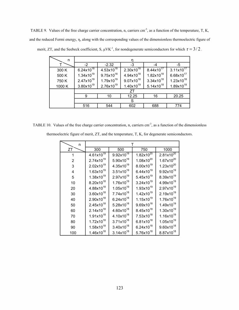
TABLE 9. Values of the free charge carrier concentration, n, carriers cm-3, as a function of the temperature, T, K,
and the reduced Fermi energy, η, along with the corresponding values of the dimensionless thermoelectric figure of
merit, ZT, and the Seebeck coefficient, S, μVK-1, for nondegenerate semiconductors for which . 2/3r =
-2 -2.32 -3 -4 -56.24x10¹⁸ 4.53x10¹⁸ 2.30x10¹⁸ 8.44x10¹⁷ 3.11x10¹⁷
1.34x10¹⁹ 9.75x10¹⁸ 4.94x10¹⁸ 1.82x10¹⁸ 6.68x10¹⁷
2.47x10¹⁹ 1.79x10¹⁹ 9.07x10¹⁸ 3.34x10¹⁸ 1.23x10¹⁸
3.80x10¹⁹ 2.76x10¹⁹ 1.40x10¹⁹ 5.14x10¹⁸ 1.89x10¹⁸
9 10 12.25 16 20.25
516 544 602 688 774
750 K1000 K
ZT
S
n η
300 KT
500 K
TABLE 10. Values of the free charge carrier concentration, n, carriers cm-3, as a function of the dimensionless
thermoelectric figure of merit, ZT, and the temperature, T, K, for degenerate semiconductors.
300 500 750 10004.61x1019 9.92x10¹⁹ 1.82x10²⁰ 2.81x10²⁰
2.74x10¹⁹ 5.90x10¹⁹ 1.08x10²⁰ 1.67x10²⁰
2.02x10¹⁹ 4.35x10¹⁹ 8.00x10¹⁹ 1.23x10²⁰
1.63x10¹⁹ 3.51x10¹⁹ 6.44x10¹⁹ 9.92x10¹⁹
1.38x10¹⁹ 2.97x10¹⁹ 5.45x10¹⁹ 8.39x10¹⁹
8.20x10¹⁸ 1.76x10¹⁹ 3.24x10¹⁹ 4.99x10¹⁹
4.88x10¹⁸ 1.05x10¹⁹ 1.93x10¹⁹ 2.97x10¹⁹
3.60x10¹⁸ 7.74x10¹⁸ 1.42x10¹⁹ 2.19x10¹⁹
2.90x10¹⁸ 6.24x10¹⁸ 1.15x10¹⁹ 1.76x10¹⁹
2.45x10¹⁸ 5.28x10¹⁸ 9.69x10¹⁸ 1.49x10¹⁹
2.14x10¹⁸ 4.60x10¹⁸ 8.45x10¹⁸ 1.30x10¹⁹
1.91x10¹⁸ 4.10x10¹⁸ 7.53x10¹⁸ 1.16x10¹⁹
1.72x10¹⁸ 3.71x10¹⁸ 6.81x10¹⁸ 1.05x10¹⁹
1.58x10¹⁸ 3.40x10¹⁸ 6.24x10¹⁸ 9.60x10¹⁸
1.46x10¹⁸ 3.14x10¹⁸ 5.76x10¹⁸ 8.87x10¹⁸
4
405060
5102030
100
n
8090
70
3
T
1ZT
2
123
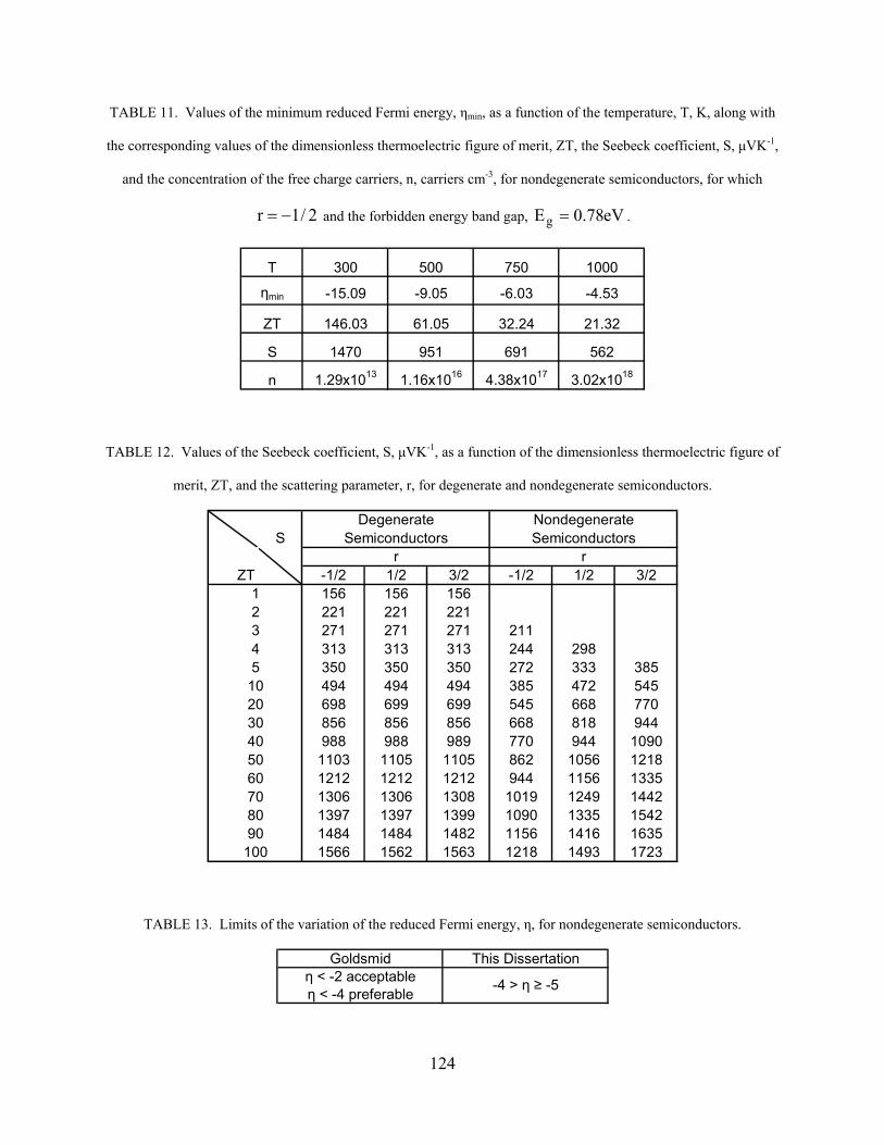
TABLE 11. Values of the minimum reduced Fermi energy, ηmin, as a function of the temperature, T, K, along with
the corresponding values of the dimensionless thermoelectric figure of merit, ZT, the Seebeck coefficient, S, μVK-1,
and the concentration of the free charge carriers, n, carriers cm-3, for nondegenerate semiconductors, for which
and the forbidden energy band gap, 2/1r −= eV78.0Eg = .
T 300 500 750 1000
ηmin -15.09 -9.05 -6.03 -4.53
ZT 146.03 61.05 32.24 21.32
S 1470 951 691 562
n 1.29x10¹³ 1.16x10¹⁶ 4.38x10¹⁷ 3.02x10¹⁸
TABLE 12. Values of the Seebeck coefficient, S, μVK-1, as a function of the dimensionless thermoelectric figure of
merit, ZT, and the scattering parameter, r, for degenerate and nondegenerate semiconductors.
ZT -1/2 1/2 3/2 -1/2 1/2 3/2156 156 156221 221 221271 271 271 211313 313 313 244 298350 350 350 272 333 385494 494 494 385 472 545698 699 699 545 668 770856 856 856 668 818 944988 988 989 770 944 1090
1103 1105 1105 862 1056 12181212 1212 1212 944 1156 13351306 1306 1308 1019 1249 14421397 1397 1399 1090 1335 15421484 1484 1482 1156 1416 16351566 1562 1563 1218 1493 1723
90100
S
50607080
10203040
2345
NondegenerateSemiconductors
r
1
DegenerateSemiconductors
r
TABLE 13. Limits of the variation of the reduced Fermi energy, η, for nondegenerate semiconductors.
Goldsmid This Dissertationη < -2 acceptableη < -4 preferable -4 > η ≥ -5
124

Chapter 8
Comparison of the Results and Findings of this
Dissertation with Those of Other Investigators
Dwelling on the topic of the upper limit or bound on the Seebeck coefficient, S, and the
thermoelectric figure of merit, ZT, Professor H.J.Goldsmid74 made the following comments in
his pioneering book on thermoelectric refrigeration:
“It is unreasonable to suppose that a single semiconductor could have the highest known
values of both carrier mobility and effective mass, since these two parameters are inter-related.
However, in estimating an upper limit of ZT, it will be supposed that a single semiconductor
does combine the very low lattice thermal conductivity derived above, which is about
, with the best known value of 11KWcm002.0 −− ( ) 2/3m/*mμ , i.e., that for bismuth at 300K,
which is about 750cm2V-1sec-2. It is also assumed that the energy gap is large enough for the
conduction to be extrinsic, when the Seebeck coefficient is optimized ( )Tk10E Bg > .
The theory of Section 3.2.1 shows that the optimum Seebeck coefficient for the
hypothetical material would be and the corresponding value of ZT is 4.1. Since a
most unlikely combination of parameters has been assumed in this estimation of the upper limit
of ZT, the situation may be summarized:
1VK350 −μ±
(i) Present trends indicate that ZT cannot be much more than unity.
(ii) It seems unlikely that ZT will exceed two.
(iii) Values of ZT greater than four seem out of the question.”
Furthermore, we now refer to earlier research work done by Rittner75 and Rittner and
125
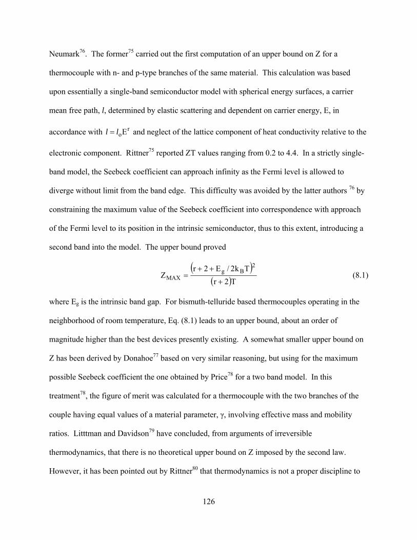
Neumark76. The former75 carried out the first computation of an upper bound on Z for a
thermocouple with n- and p-type branches of the same material. This calculation was based
upon essentially a single-band semiconductor model with spherical energy surfaces, a carrier
mean free path, l, determined by elastic scattering and dependent on carrier energy, E, in
accordance with and neglect of the lattice component of heat conductivity relative to the
electronic component. Rittner75 reported ZT values ranging from 0.2 to 4.4. In a strictly single-
band model, the Seebeck coefficient can approach infinity as the Fermi level is allowed to
diverge without limit from the band edge. This difficulty was avoided by the latter authors 76 by
constraining the maximum value of the Seebeck coefficient into correspondence with approach
of the Fermi level to its position in the intrinsic semiconductor, thus to this extent, introducing a
second band into the model. The upper bound proved
roEll =
( )
( )T2rTk2/E2r
Z2
BgMAX +
++= (8.1)
where Eg is the intrinsic band gap. For bismuth-telluride based thermocouples operating in the
neighborhood of room temperature, Eq. (8.1) leads to an upper bound, about an order of
magnitude higher than the best devices presently existing. A somewhat smaller upper bound on
Z has been derived by Donahoe77 based on very similar reasoning, but using for the maximum
possible Seebeck coefficient the one obtained by Price78 for a two band model. In this
treatment78, the figure of merit was calculated for a thermocouple with the two branches of the
couple having equal values of a material parameter, γ, involving effective mass and mobility
ratios. Litttman and Davidson79 have concluded, from arguments of irreversible
thermodynamics, that there is no theoretical upper bound on Z imposed by the second law.
However, it has been pointed out by Rittner80 that thermodynamics is not a proper discipline to
126
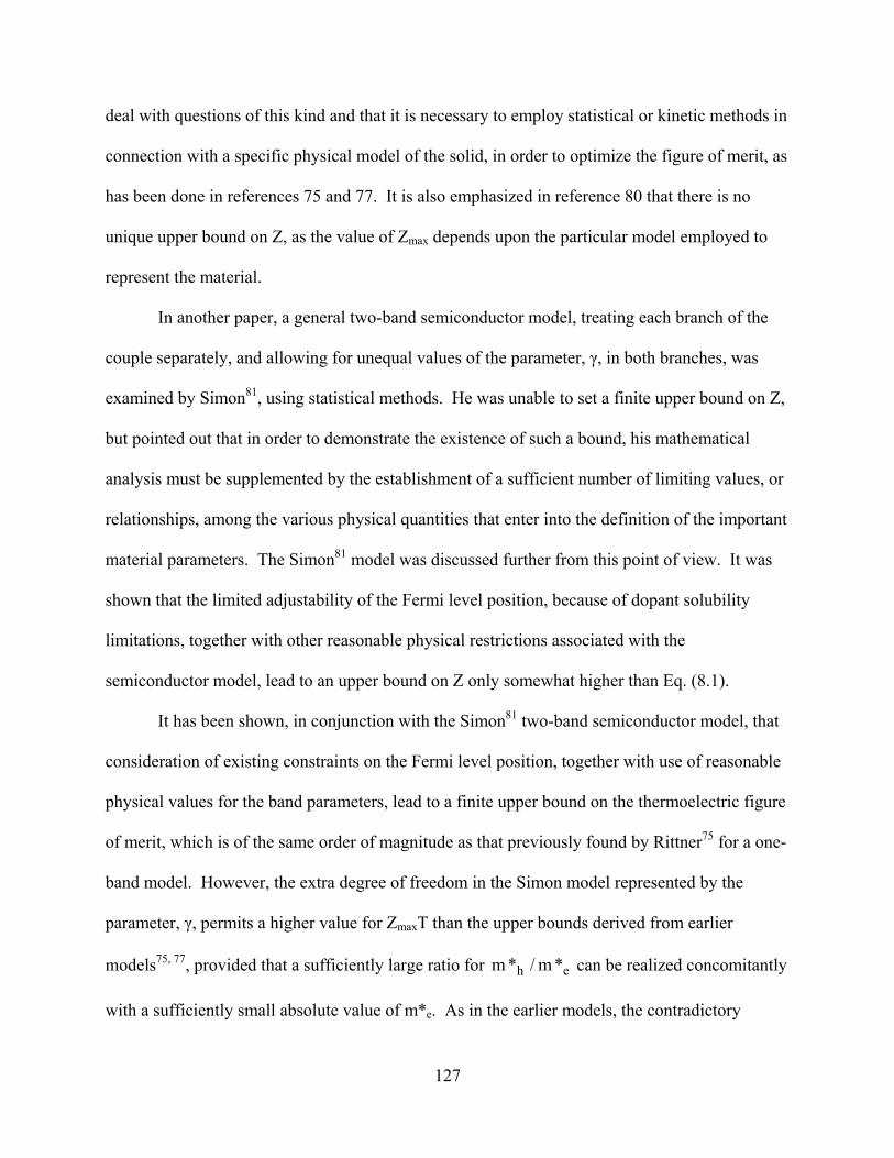
deal with questions of this kind and that it is necessary to employ statistical or kinetic methods in
connection with a specific physical model of the solid, in order to optimize the figure of merit, as
has been done in references 75 and 77. It is also emphasized in reference 80 that there is no
unique upper bound on Z, as the value of Zmax depends upon the particular model employed to
represent the material.
In another paper, a general two-band semiconductor model, treating each branch of the
couple separately, and allowing for unequal values of the parameter, γ, in both branches, was
examined by Simon81, using statistical methods. He was unable to set a finite upper bound on Z,
but pointed out that in order to demonstrate the existence of such a bound, his mathematical
analysis must be supplemented by the establishment of a sufficient number of limiting values, or
relationships, among the various physical quantities that enter into the definition of the important
material parameters. The Simon81 model was discussed further from this point of view. It was
shown that the limited adjustability of the Fermi level position, because of dopant solubility
limitations, together with other reasonable physical restrictions associated with the
semiconductor model, lead to an upper bound on Z only somewhat higher than Eq. (8.1).
It has been shown, in conjunction with the Simon81 two-band semiconductor model, that
consideration of existing constraints on the Fermi level position, together with use of reasonable
physical values for the band parameters, lead to a finite upper bound on the thermoelectric figure
of merit, which is of the same order of magnitude as that previously found by Rittner75 for a one-
band model. However, the extra degree of freedom in the Simon model represented by the
parameter, γ, permits a higher value for ZmaxT than the upper bounds derived from earlier
models75, 77, provided that a sufficiently large ratio for can be realized concomitantly
with a sufficiently small absolute value of m*e. As in the earlier models, the contradictory
eh *m/*m
127

conditions persist that the lattice component of the heat conduction be as small as possible and
the band gap as large as possible. Peculiar to the Simon two-band model is the requirement that
acoustic lattice scattering be the predominant process determining the mobility in the negative
branch of the couple and that impurity scattering be the dominant one in the positive branch of
the couple. Also, in the negative branch, it is desirable that there be a large number of equivalent
extrema in the conduction band and a small number in the valence band, that there be a large
mass anisotropy for the electrons but not for the holes, and that the deformation potential for the
valence band edge be much larger than that for the conduction band edge. The first two of these
three factors (with conduction and valence band reversing roles) are also somewhat useful in the
positive branch.
It is abundantly evident that most, if not all, of the assumptions and arguments made by
the aforementioned authors75-81, particularly those indicated by Simon81, have a very remote
chance of eventually being realized in practice. Not surprisingly, they ended up being attacked
and challenged by Wood82. The latter’s main argument runs as follows: Rittner and Neumark83
and Donahoe77 have argued that the maximum S, and hence maximum Z, will occur when the
Fermi level is at the middle of the band gap, Eg. They assumed extrinsic n-type material, with
and , since contributions from charge carriers of the opposite sign (holes)
will otherwise reduce the value of S in the expression for the total Seebeck coefficient, which is
np *m*m > np μ<<μ
pn
ppnn SSS
σ+σ
σ+σ= (8.2)
Hence they obtain
( )
ATTk2/EA
Z2
Bg+= (8.3)
Since there is no theoretical limit to the band gap, obviously there is no theoretical limit to the
128

magnitude of Z. Similar, but more refined, arguments, by other investigators, considering
bipolar conduction, have essentially concluded that the upper limit on Z is governed by the value
of the energy gap and the mobility ratio, i.e., in every case, it was found that no theoretical upper
bound could be placed on Z. This conclusion is supported by the work of Littman and
Davidson79 who derived Z using irreversible thermodynamics and found a theoretical upper
bound of infinity. In lieu of a theoretical limit, likely values of the relevant parameters have
been substituted in the equations of Rittner and Neumark83 and Donahoe77 to obtain typical Zmax
values 82 of about . These Z values are far in excess of those found
experimentally todate.
13 K104517 −−×−
Now, before closing this section on the comparison of our results with those of other
investigators, we thought it worthwhile to try to derive, or prove the validity of, Eq. (8.1), which
corresponds to, or is identical with, Eq. (21) in Rittner’s75 paper, Eq. (1) in Rittner and
Neumark’s76 paper and Eq. (3.29) in Dr. C. Wood’s82 research report. We will rewrite the latter
equation below in order to make our discussion easier and more clearly understood
( )( )
ATk2/EA
ZT2
BgMAX
+= (8.4)
Now there should be no doubt whatsoever that this whole analysis deals exclusively with
nondegenerate semiconductors. Also, earlier in this dissertation, when we decided to lower the
reduced Fermi energy, η, until the middle of the forbidden energy band gap, also known as the
intrinsic Fermi energy level, in order to maximize the value of ZT, we ended up deriving Eqs.
(7.39-7.41). Now invoking Eqs. (5.8) and (5.9), substituting the value of η, according to Eq.
(7.41), into Eq. (5.8) and then substituting both Eqs., (5.8) and (5.9), into Eq. (5.6), we finally
obtain
129
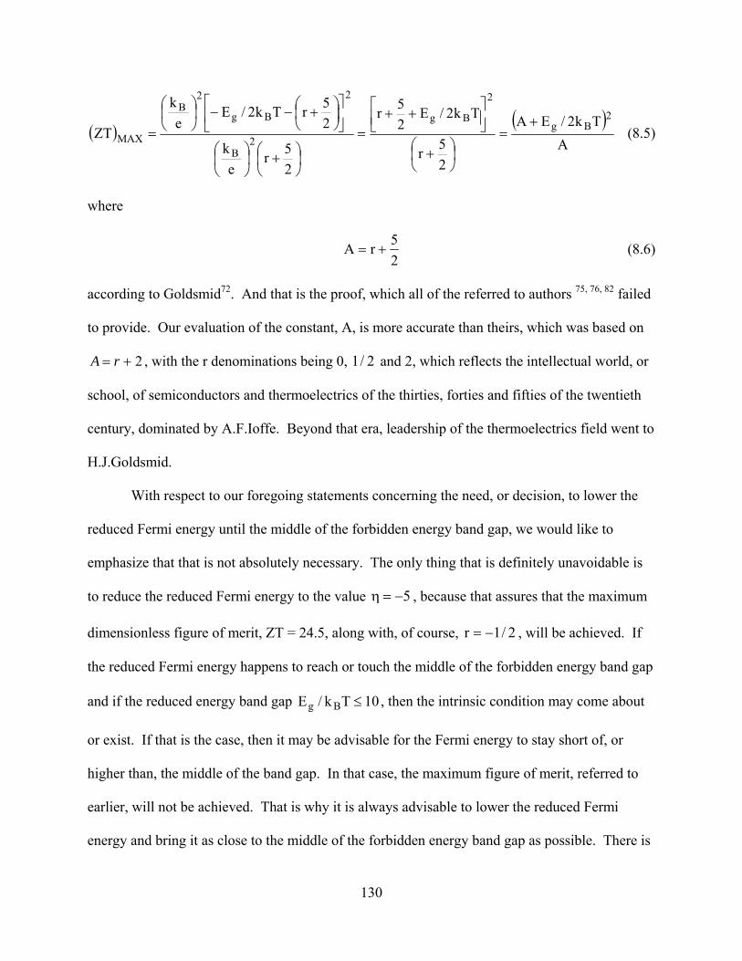
( )( )
ATk2/EA
25r
Tk2/E25r
25r
ek
25rTk2/E
ek
ZT2
Bg
2
Bg
2B
2
Bg
2B
MAX+
=⎟⎠⎞
⎜⎝⎛ +
⎥⎦⎤
⎢⎣⎡ ++
=
⎟⎠⎞
⎜⎝⎛ +⎟
⎠⎞
⎜⎝⎛
⎥⎦
⎤⎢⎣
⎡⎟⎠⎞
⎜⎝⎛ +−−⎟
⎠⎞
⎜⎝⎛
= (8.5)
where
25rA += (8.6)
according to Goldsmid72. And that is the proof, which all of the referred to authors 75, 76, 82 failed
to provide. Our evaluation of the constant, A, is more accurate than theirs, which was based on
2+= rA , with the r denominations being 0, and 2, which reflects the intellectual world, or
school, of semiconductors and thermoelectrics of the thirties, forties and fifties of the twentieth
century, dominated by A.F.Ioffe. Beyond that era, leadership of the thermoelectrics field went to
H.J.Goldsmid.
2/1
With respect to our foregoing statements concerning the need, or decision, to lower the
reduced Fermi energy until the middle of the forbidden energy band gap, we would like to
emphasize that that is not absolutely necessary. The only thing that is definitely unavoidable is
to reduce the reduced Fermi energy to the value 5−=η , because that assures that the maximum
dimensionless figure of merit, ZT = 24.5, along with, of course, 2/1r −= , will be achieved. If
the reduced Fermi energy happens to reach or touch the middle of the forbidden energy band gap
and if the reduced energy band gap 10Tk/E Bg ≤ , then the intrinsic condition may come about
or exist. If that is the case, then it may be advisable for the Fermi energy to stay short of, or
higher than, the middle of the band gap. In that case, the maximum figure of merit, referred to
earlier, will not be achieved. That is why it is always advisable to lower the reduced Fermi
energy and bring it as close to the middle of the forbidden energy band gap as possible. There is
130

no other alternative.
In our foregoing analysis and review of the research reports of a number of other
investigators 74-83, we have been exposed to a large number of arguments and counterarguments
as to whether there exists an upper bound or limit on Eg, S and, more importantly, on Z and/or
ZT. Both the opponents and proponents of the upper bound on ZT are making wonderful
expositions in support of their respective points of view. Some of them are going as far as to
suggest
Tk16E Bg = (8.7)
as their preferred or recommended value for the forbidden energy band gap, which, obviously,
applies only to nondegenerate semiconductors and, therefore, has nothing to do with degenerate
ones. Of course, the higher the value of Eg, the higher will ZT be according to any of Eqs. (8.1)
and (8.3-8.5). Such high values as 16 for the reduced energy band gap, nevertheless, are no
longer acceptable nowadays. The maximum η value recommended at present for good
thermoelectric materials is 10, so that Eq. (8.7) becomes
Tk10E Bg = (8.8)
In thermoelectrics, as in many other fields, more is not necessarily always better. A very large
energy band gap should be regarded always with suspicion, because that implies a greater
difficulty for free electrons to be generated and move around, which ends up lowering the
electrical conductivity until it becomes zero. For best results, energy band gaps must be neither
too narrow nor too wide. That is why semiconductors, with their moderately-sized energy band
gaps, are the materials most indicated and recommended for thermoelectric energy conversion.
According to Pierre Aigrain84, a reasonable energy band gap for power generation purposes
should be about 0.6eV. For refrigeration, that value goes down to about 0.3eV.
131

Let us now try to see and analyze what happens if we move away from semiconductors to
either metals or dielectric and ionic materials:
For metals, 0 and S is very small, thus L ≅κ
L
SLT
TSTSZT22
e
2=
σσ
=κσ
= (8.9)
and because S is very small, metals are not appropriate for thermoelectric energy conversion, but
they can still be used as thermocouples for temperature measurement.
For dielectric and ionic materials, 0≅σ and S is very high, or enormous, therefore
0TSZTL
2=
κσ
= (8.10)
because , as a consequence to the fact that there are no free electrons available to carry the
electric charge and thus conduct electricity. Thus, despite their very high S, dielectric and ionic
materials are not suitable for thermoelectric energy conversion.
0≅σ
Thus, only semiconductors with their moderately wide energy band gaps are the materials
most suited for direct thermoelectric energy conversion.
Referring now to the possible upper bounds or limits on ZT that we discussed earlier,
what we must say here is that yes, these limits or bounds do exist. We actually did impose those
limits on the maximum possible ZT values for degenerate and nondegenerate semiconductors,
while at the same time, we were totally unaware that we were doing so. These bounds or limits
actually came about as a natural consequence to, or outcome of, our entire research work on this
dissertation, not because we were looking for ways to impose them in order to satisfy, or be
responsive to, any preconceived concepts or notions we might have had in relation thereto.
These bounds or limits became known to us only after most of the research work on this
dissertation had already been carried out. The limits or bounds that we have found out were that
132

for nondegenerate semiconductors, the maximum possible figure of merit ZT=24.5, or about 25,
and that for degenerate semiconductors, the maximum possible ZT=23.85, or about 24. So, we
many end up writing a generic equation for both types of semiconductors
( ) 25ZT MAX ≤degenerate
atenondegener (8.11)
For degenerate semiconductors, the limit was imposed quite naturally by the fact that in
order to achieve a ZT value greater than 23.85, the material would have had to behave as a
nondegenerate semiconductor, i.e., the rules and equations of degenerate semiconductors were
not applicable any more beyond that ZT value of 23.85. We thus had a case of reductio ad
absurdum. For nondegenerate semiconductors, the situation was completely different, since the
limit was imposed when we tried to lower the Fermi energy down to the middle of the forbidden
energy band gap, which is also known as the intrinsic Fermi level. And since we knew that we
couldn’t lower or push the Fermi level any further below the intrinsic level, therefore, that
imposed the upper bound or limit on ZT for nondegenerate semiconductors which, as we already
know, is . ( ) 5.24ZT MAX =
When we began our research work on this dissertation, we reviewed the theoretical
fundamentals of thermoelectric energy conversion and the transport of heat and electricity in
solids. We then quickly derived Eq. (5.6) and a number of other relationships, up to Eq. (5.25),
and ended up constructing Table (1). As soon as we had done that, we remained with the secret
inner notion and hope that the maximum ZT value that would possibly be achieved would lie
somewhere in the middle of the entire spectrum of ZT values presented, maybe 40 and probably
even 50. Unfortunately, however, our initial inner secret hope or belief concerning the
maximum ZT value achievable with either nondegenerate, or degenerate, semiconductors will
133
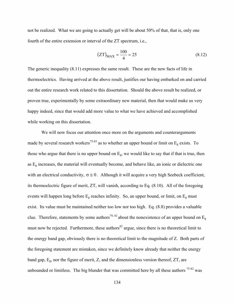
not be realized. What we are going to actually get will be about 50% of that, that is, only one
fourth of the entire extension or interval of the ZT spectrum, i.e.,
( ) 254
100ZT MAX == (8.12)
The generic inequality (8.11) expresses the same result. These are the new facts of life in
thermoelectrics. Having arrived at the above result, justifies our having embarked on and carried
out the entire research work related to this dissertation. Should the above result be realized, or
proven true, experimentally by some extraordinary new material, then that would make us very
happy indeed, since that would add more value to what we have achieved and accomplished
while working on this dissertation.
We will now focus our attention once more on the arguments and counterarguments
made by several research workers75-83 as to whether an upper bound or limit on Eg exists. To
those who argue that there is no upper bound on Eg, we would like to say that if that is true, then
as Eg increases, the material will eventually become, and behave like, an ionic or dielectric one
with an electrical conductivity, . Although it will acquire a very high Seebeck coefficient,
its thermoelectric figure of merit, ZT, will vanish, according to Eq. (8.10). All of the foregoing
events will happen long before Eg reaches infinity. So, an upper bound, or limit, on Eg must
exist. Its value must be maintained neither too low nor too high. Eq. (8.8) provides a valuable
clue. Therefore, statements by some authors79, 82 about the nonexistence of an upper bound on Eg
must now be rejected. Furthermore, these authors82 argue, since there is no theoretical limit to
the energy band gap, obviously there is no theoretical limit to the magnitude of Z. Both parts of
the foregoing statement are mistaken, since we definitely know already that neither the energy
band gap, Eg, nor the figure of merit, Z, and the dimensionless version thereof, ZT, are
unbounded or limitless. The big blunder that was committed here by all these authors 75-82 was
0≅σ
134

their introduction of Eg into the equations for Z or ZT. Therefore, if Eg were considered, or
assumed to be, unbounded, then also ZT would consequently become unbounded or limitless.
That again is another case of reductio ad absurdum. These authors have considered only the
mathematics of the problem and ignored the physics thereof. That is where they went wrong. In
this dissertation, we have established that the thermoelectric figure of merit, ZT, is indeed
bounded for both nondegenerate and degenerate semiconductors, with the maximum value or
limit being 24.5 and 23.85, respectively. These two limits were not obtained as a result of any
superficial assumption or quick and careless evaluation, but were the outcome of a thorough,
persistent and prolonged research effort that lasted more than two years. Consequently, we reject
the range of values for ( ) of 17-45 (T = 1000K), reported by C. Wood82, and mentioned
earlier in this section, as unreliable.
MAXZT
Lin, Sun and Dresselhaus85 have recently developed a theoretical model for the transport
properties of cylindrical Bi nanowires. Based on the band structure of Bi nanowires and the
semiclassical transport model, the thermoelectric figure of merit, ZT, was calculated for Bi
nanowires, with various wire diameters and wire orientations. Their results show that the
trigonal axis is the most favorable wire orientation for thermoelectric applications, and is
predicted for n-type trigonal wires with diameters
1ZT >
nm10dW < . The effect of T-point holes on
the thermoelectric performance has also been discussed, and it was found that ZT can be
significantly enhanced, especially for p-type nanowires, if T-point holes are removed or
suppressed, which can possibly be achieved by Sb doping. The entire investigation was carried
out at only one temperature, namely 77K. ZT values of about 2 and 6 were obtained or
calculated for n-type Bi nanowires having diameters of 10 and 5 nm, respectively. It was found
that the thermoelectric performance substantially decreases as the diameter of the Bi nanowires
135

increases. A similar thermoelectric performance was obtained, or calculated, for p-type Bi
nanowires.
Lin et al.’s results are encouraging and appear to be useful for temperatures well below
room temperature, i.e., for refrigeration. It is unlikely that they can be extrapolated or extended
to temperatures above room temperature. It is therefore, highly unlikely that they can be used for
power generation applications. At temperatures well above room temperature, the Seebeck
coefficient tends to increase substantially above its room temperature value, and since
at temperatures higher than room temperature, there is no way for Lin’s results to be
applicable or competitive here.
L/SZT 2=
In a recent report or article, Professor H. J. Goldsmid86, who in 196474 had stated that ZT
cannot be much more than 1, that it seems unlikely that ZT will exceed 2 and that values of ZT
greater than 4 seem out of the question, now comes and tries to convince us that the figure of
merit of new bulk thermoelectric materials cannot exceed the limit of ZT = 4. In establishing
this new limit, Professor Goldsmid is basing his argument on the assumption that any promising
figure of merit of new bulk thermoelectric materials is due entirely to their very low thermal
conductivity, which already has its minimum value. We strongly disagree with Professor
Goldsmid on this issue and we believe that the limit on the figure of merit of these materials
, that is, 6 times greater than the limit established by him. In reaching that
conclusion, we have removed the lattice thermal conductivity entirely from any equations we
might have used to calculate ZT for semiconductors. To this effect, we used the very simple,
elegant and very powerful equation that represents the cornerstone of this investigation, which is
( ) 25ZT MAX =
L
SZT2
=
136

Professor Goldsmid, obviously encouraged by Lin et al.’s85 results on Bi-based
nanowires, or quantum wires, has suggested that a minimum lattice conductivity Lκ of 0.1Wm-
1K-1, coupled with a power factor, S2σT, of 103.9Wm-1K-1 at 77K and a Seebeck coefficient, S,
of 630μVK-1, would yield a ZT value of about 20. Professor Goldsmid suggested, furthermore,
that the aforementioned value, ZT=20, will remain the same, even if the temperature is increased
from 77K to 300K. Professor Goldsmid pushed his ideas and concepts much further, saying:
“We might go further and propose that ZT might have a limiting value of about 20 at all
temperatures of practical interest.” Professor Goldsmid finally concluded his report making the
following statements: “It has been shown that there is no reason to raise the upper bound for the
dimensionless figure of merit above four for bulk thermoelectric devices but there are good
grounds for supposing that a value as high as 20 might be reached using low-dimensional
structures. It is possible that a still greater value might be reached if one can realize the situation
in which the electron and phonon flows are independent of one another. If, indeed, ZT were to
reach a value of about 20, then the performance at ordinary temperatures would be similar to that
of a vacuum diode with a cathode having a work function of 0.3 eV.”
We strongly disagree with many of the statements of Professor Goldsmid. His reference
to the value of the minimum lattice thermal conductivity as being no more than about 0.1 to 0.2
Wm-1K-1 is not true. The research reports on that matter that came to our attention, thus far, say
otherwise. They indicate that the minimum lattice thermal conductivity for bulk materials is
about 0.3Wm-1K-1. Also the value of the lattice thermal conductivity Lκ remains important as
long as which is true for low temperatures and for applications where doping is
moderate, i.e., refrigeration. But when we go to temperatures substantially higher than room
temperature, coupled with mass and volume fluctuation scattering of phonons, along with
eL κ>>κ
137

moderate to heavy doping, what we get is eL κ<<κ , so Lκ becomes negligible or unimportant.
We don’t care how much its value is, we just neglect it. That is the main difference between the
low temperature and the high temperature domains, or ranges, in thermoelectrics. They are
governed by different laws. So the fact that the highest observed value for is 0.075
m2V-1sec-1 for electrons in Bi is of no interest to us in the temperature range above room
temperature. Also the Seebeck coefficient value, S=630μVK-1, as well as the lattice thermal
conductivity value, =0.1 Wm-1K-1, are only assumed values. They have not been
corroborated experimentally.
( ) 2/3m/*mμ
Lκ
In response to Professor Goldsmid’s assertions, setting a limit, or bound, of four on the
dimensionless thermoelectric figure of merit of new bulk thermoelectric materials, i.e.,
( ) 4ZTbulk
max=
we would like to carry out an experimental research program aiming at producing and evaluating
the thermoelectric performance of the following four component material:
Mg-Si-Pb-Ba
Production of the aforementioned material through any appropriate process or method,
such as melting or by using the powder metallurgy technique, or any other method, will end up
bringing about a quaternary alloy or solid solution of intermetallic compounds containing
magnesium silicide, magnesium plumbide, barium silicide and barium plumbide, wherein the
alloy or solid solution is defined by the following chemical constitutional formula:
( ) ( ) xx1r12r2 PbSiMgBa −−
wherein r, , and x represent the atomic or molecular proportion of each of barium,
magnesium, silicon and lead in the alloy, respectively, and wherein r varies from 0.1 to 0.4 and x
( )r−1 ( x−1 )
138

varies from 0.1 to 0.3.
The objective would be to prepare doped and undoped samples of this material by any
appropriate method and then measure the following three properties:
(1) Seebeck Coefficient
(2) Electrical Conductivity
(3) Thermal Conductivity
We would then calculate the dimensionless figure of merit as follows
κσ
=TSZT
2
All the measurements should be carried out at various temperatures ranging from 300K to
1000K. In the above expression for ZT, σ and κ will tend to cancel out, because is very
small or negligible. So S becomes the crucial parameter that determines how good the material
is thermoelectrically. This fact can be expressed by the following equation
Lκ
L
SZT2
=
where L is the Lorenz number, whose value depends on the concentration of the free charge
carriers, whether it is equal to or less than carriers cm-3, in which case we have a
nondegenerate semiconductor, which implies that L depends on the value of the scattering
parameter or index, r, whether it is , or . If the concentration of the free charge
carriers is greater than carriers cm-3, we then have a degenerate semiconductor and the
value of L in that case will be the same as that for metals, as well as independent of r.
19105.2 ×
2/1− 2/1 2/3
19105.2 ×
In 1995, Slack30 wrote that there has long been an interest in the question of the ultimate
performance limits for thermoelectric materials, both for generators and for coolers. Since Z
depends inversely on the thermal conductivity of the material from which the device is made, it
139
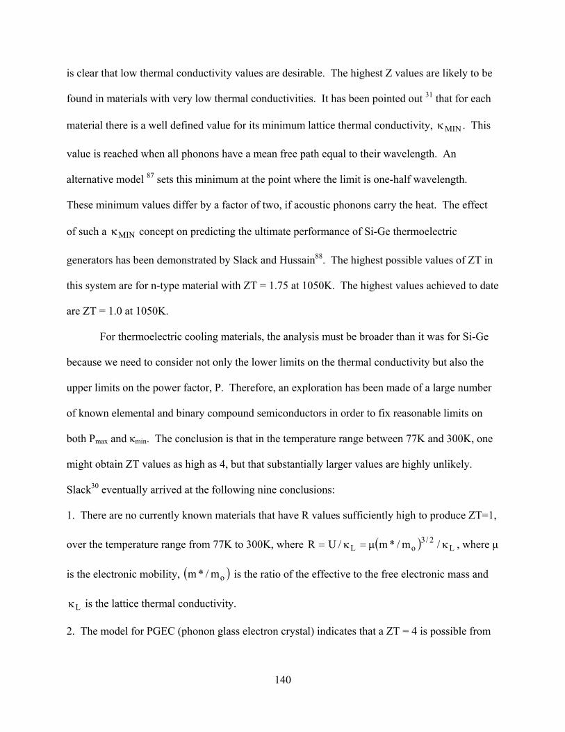
is clear that low thermal conductivity values are desirable. The highest Z values are likely to be
found in materials with very low thermal conductivities. It has been pointed out 31 that for each
material there is a well defined value for its minimum lattice thermal conductivity, . This
value is reached when all phonons have a mean free path equal to their wavelength. An
alternative model 87 sets this minimum at the point where the limit is one-half wavelength.
These minimum values differ by a factor of two, if acoustic phonons carry the heat. The effect
of such a concept on predicting the ultimate performance of Si-Ge thermoelectric
generators has been demonstrated by Slack and Hussain88. The highest possible values of ZT in
this system are for n-type material with ZT = 1.75 at 1050K. The highest values achieved to date
are ZT = 1.0 at 1050K.
MINκ
MINκ
For thermoelectric cooling materials, the analysis must be broader than it was for Si-Ge
because we need to consider not only the lower limits on the thermal conductivity but also the
upper limits on the power factor, P. Therefore, an exploration has been made of a large number
of known elemental and binary compound semiconductors in order to fix reasonable limits on
both Pmax and κmin. The conclusion is that in the temperature range between 77K and 300K, one
might obtain ZT values as high as 4, but that substantially larger values are highly unlikely.
Slack30 eventually arrived at the following nine conclusions:
1. There are no currently known materials that have R values sufficiently high to produce ZT=1,
over the temperature range from 77K to 300K, where ( ) L2/3
oL /m/*m/UR κμ=κ= , where μ
is the electronic mobility, is the ratio of the effective to the free electronic mass and
is the lattice thermal conductivity.
( om/*m )
Lκ
2. The model for PGEC (phonon glass electron crystal) indicates that a ZT = 4 is possible from
140

77K to 300K if a mat 0 cm2V-1s-1 anderial with U = 180 5.2L =κ mWcm-1K-1 can be found.
-1V-1.
e found.
d-gap, hea y element compound
The decisive ratio is 20.7/UR L =κ= cm2s2Kg
3. It seems unlikely that cooling materials with 4ZT > will ever b
4. The goal of ZT=1 can be obtained with R=0.60 cm2s2Kg-1V-1.
5. The place to look for such materials is in small-ban v
semiconductors, with electronegativity differences of 5.0X ≤Δ .
6. For doping levels less than 1019cm-3 charged impurity scattering that might lower the mobility
on to
rs increases as
will be screened out by the high dielectric constants.
7. For ZT = 4 materials, the traditional use of mixed crystal formati enhance the ZT values
will fail because alloy scattering of the charge carrie [ ]2XΔ . There are very few
pairs of elements with small XΔ values available.
8. For ZT = 1 materials, mixed crystals might help in a few special cases.
9. Minimum thermal conductivity values can sometimes be found in crystals that contain
temperature. He also stated that the figure of merit, Z, for a thermoelectric material is given
“rattling” atoms or molecular groups.
In his research report, Slack30 wrote that a model thermoelectric material is “a phonon
glass and an electron crystal.” Its ZT values are calculated as a function of carrier concentration
and
by
TOT
2SZκ
σ= (8.13)
where
TLLTOT σ+κ=κ (8.14)
141

where S = Seebeck coefficient, σ = electrical conductivity, κL = lattice thermal conductivity, L =
Lorenz number and T = absolute temperature. This can be rewritten as:
( )⎥⎦⎤
⎢⎣⎡ κ
=L/SZT
σ+
TL1 L
2
(8.15)
If , then Eq. (8.15) becomes eL TL κ=σ<<κ
L
ZT2
= (8.16)
which is identical with Eqs. (5.6) or (5.7), and which is mainly applicable in the high temp
range, above room temperature, that is, for thermoelectric power generation. For temperatures
well below room temperature, namely refrigeration, and especially if κL has not also been
substantially reduced through mass and volume fluctuation scattering of the phonons, or throu
any other means, then Eq. (8.15) will have to be used rather than Eq. (8.16). And in
the value of ZT will be lower than that calculated according to Eq. (8.16). That is the major
difference between low temperature and high temperature a
S
erature
gh
that case,
pplications, as far as the
dimensionless thermoelectric figure of merit, ZT, is concerned. Slack30 correctly stated that his
results were mainly related to thermoelectric refrigeration.
142
Chapter 9
General Summary and Conclusions
In this dissertation, we have started our research by deriving an equation for calculating
an equation for calculating an effective dimensionless thermoelectric figure of merit, ZT, which
constitutes a departure from the earlier equation established by Altenkirch. The traditional
Altenkirch equation has been used by almost all research workers in thermoelectrics since the
beginning of the twentieth century. In order to enable the derivation of the new equation for the
effective ZT, and make it stand on a firm foundation with little or negligible error, the phonon or
lattice component of the thermal conductivity, of the material used in the manufacture of the
thermoelectric energy conversion device, must be reduced to a negligible value compared to the
electronic component thereof. One way of achieving this, for temperatures higher than room
temperature, is to use alloys or solid solutions, comprising at least three or four different
elements, where mass and volume fluctuation scattering, or alloy scattering, of phonons is
predominant. The foregoing is obviously related to thermoelectric power generation. For low
temperature applications of thermoelectrics, notably refrigeration, rattlers, quantum wells,
superlattices, clathrates, etc., are currently often used to reduce the lattice thermal conductivity.
Values from 0.001 to 0.002 Wcm-1K-1 for the minimum phonon thermal conductivity have been
reported in the literature. In the opinion of most experts in the field, the minimum phonon
thermal conductivity should be no greater than 0.003 Wcm-1K-1 at room temperature. For
thermoelectric energy conversion devices operating in the temperature range of 300-1000K, the
phonon thermal conductivity should be further lowered to 0.0009 Wcm-1K-1 at the higher
temperature limit of 1000K, according to the Eucken inverse temperature law for semiconductor
143

alloys and solid solutions. This already should give us an enormous headway in the design of
future thermoelectric devices for power generation. Since the phonon thermal conductivity of
the semiconducting materials that we use for thermoelectric energy conversion does not go to
zero, we have to make sure that the ratio of the electronic thermal conductivity to the phonon
thermal conductivity is much greater than unity, in order to assure the validity of the equation,
ZT=S2/L, that we derived for the effective dimensionless thermoelectric figure of merit, where S
is the Seebeck coefficient and L is the Lorenz number. For that purpose, several equations have
been derived expressing the ratio of the electronic to the phonon, or lattice, thermal conductivity
for the various values of the electron scattering parameter, r, namely: -1/2, 1/2 and 3/2, for both
nondegenerate and degenerate semiconductors.
When one compares the effective ZT equation with the earlier equation due to
Altenkirch, one notices that out of the three properties involved in the latter equation for ZT, two
are missing in the effective ZT equation, which are the electrical conductivity and the thermal
conductivity. We have thus ended up retaining only one property, namely the Seebeck
coefficient, in the newer equation. Over the years, the best way to improve or optimize the
performance of thermoelectric devices has been to maximize the product, S2σ, known as the
power factor, in the numerator of the Altenkirch equation, by taking its derivative and equating it
to zero, i.e., ∂(S2σ)/∂σ = 0. This has led, or contributed, to the idea or concept of optimum
doping, which leads to drastically increased σ with virtually little variation in S, and thus (S2σ) is
maximized. However, thanks to the Wiedemann-Franz law, the electronic component of the
overall thermal conductivity, which is in the denominator of the Altenkirch equation, also
increases in proportion to the σ increase. This leads to an increase in the total thermal
conductivity, which is always undesirable, because it tends to reduce or eliminate the effect of
144
increasing the power factor, (S2σ). This kind of situation is called: “Conservation of nastiness.”
We indeed do have conservation of nastiness in thermoelectrics, because, while on the one hand
we increase the numerator through maximizing the power factor, yet on the other hand, the
denominator of the Altenkirch equation also increases, owing to the Wiedemann-Franz law. In
this dissertation, through our derivation and use of the effective ZT, we have put an end to this
conservation of nastiness and eliminated that vicious circle, once and for all, particularly in the
temperature range above room temperature, notably for power generation applications.
Next, we moved forward to the most important part of this investigation. New
relationships have been worked out for the effective ZT as a function of the reduced Fermi
energy, η, and the scattering parameter, r, for nondegenerate semiconductors. We elaborated
correlations of the reduced Fermi energy, η, and the effective ZT as functions of the free charge
carrier concentration, n, and the absolute temperature, T. This elaboration was done for values
of the scattering parameter of -1/2, 1/2 and 3/2. For nondegenerate semiconductors, we
calculated the values of ZT for certain values of η randing from -2 to -5, and we also calculated
the corresponding values of S. We also developed an independent correlation for η as a function
of n and T, which we converted into another relationship giving n as a function of η and T. We
then used all of the foregoing to construct three tables giving the values of n, ZT and S for the
aforementioned values of η and values of T from 300K to 1000K. We carried out these
calculations for r = -1/2, 1/2 and 3/2. For degenerate semiconductors, we developed an
independent relationship for ZT as a function of T and n. This relationship was then converted
into a new one giving n as a function of T and ZT. We then used this new equation to construct
one additional table giving values of n for certain values of ZT ranging from 1 to 100, and the
predetermined values of T of 300K, 500K, 750K and 1000K.
145
On the basis of the numerical data presented in the aforementioned four tables, we
were able to draw the following conclusions:
1. The highest ZT value possible for a nondegenerate semiconductor is 24.5 and is achieved
through a material for which r = -1/2, η = -5 and S = 602 μVK-1.
2. The highest ZT value possible for a degenerate semiconductor is 23.9 and is achieved through
a material for which T = 1000K, n = 2.6x1019 cm-3 and S = 764μVK-1.
3. Comparing the foregoing value for S, namely, S = 764μVK-1, with the earlier one for the
nondegenerate semiconductor having the highest ZT value of 24.5 and S = 602μVK-1, it may be
noticed that the nondegenerate material places a substantially lesser requirement on S than the
degenerate one. The higher the demand on the Seebeck coefficient, the less likely it is that such
a demand will be realized in practice. For that reason, and bearing in mind that the two ZT
values are almost identical, we end up adopting the nondegenerate semiconductor, as the
material of preference.
More generally, we should select nondegenerate in preference to degenerate
semiconductors for thermoelectric energy conversion applications. Nondegenerate
semiconductors require far lesser doping than degenerate ones. As mentioned earlier, they also
require a lower Seebeck coefficient than the degenerate semiconductors for the same ZT value,
especially those for which r = -1/2. Therefore, nondegenerate semiconductors for which r = -1/2
and, if at all possible, η = -5, that is, with relatively little doping, should be our materials of
preference for thermoelectric energy conversion, particularly for power generation applications.
That is perhaps the most important conclusion of this dissertation.
The key to success in this research program, and the results and conclusions originating
therefrom is to assure the validity of the equation, ZT = S2/L. This definitely comes about
146

through the near elimination of the lattice thermal conductivity. The latter has been the main
culprit hindering the progress of thermoelectricity throughout the twentieth century.
147

Appendix 1
General Review of the Brillouin Zone Concept
The face-centered and body-centered cubic lattices have been proven to be mutually
reciprocal. A face-centered cubic lattice has a body-centered cubic lattice as its reciprocal.
Wave propagation in a periodic medium for three dimensions has a general solution given by the
equation where A(r) is the amplitude, υ is the frequency, a is the
reciprocal of the wavelength (1/λ) and r is the distance, from some point in a cell (n1,n2,n3) to the
origin of the first cell r = ro+r΄+n1d1+ n2d2+ n3d3. This is the basis of the Wigner-Seitz method of
the theory of solids. Thus the wave motion of particles in a discontinuous lattice is given by
( )[{ r.atυi2exp)r(A −π=Ψ ]}
)]
)]
([ 332211jj knknkntiexpA −−−ω=Ψ where kj = 2πaj = 2π/λ is the wave vector. This is the
wave function inside the cell (n1,n2,n3), or
([ 332211 knknkntiexp)'r(''A −−−ω=Ψ . Wigner and Seitz choose their elementary cell in
a manner similar to that in which zones are constructed for the reciprocal lattice, i.e. by
constructing a polyhedron about a lattice point. The faces of the polyhedron are planes that are
perpendicular bisectors of the lines joining the points taken as the origin with neighboring lattice
points. The motion of electrons in a potential field (x,y,z), e.g. free electrons in a metal, is
obtained from the solution of the Schrödinger equation ( ) 0VEk 22 =Ψ−+Ψ∇ where
22
2 m2h
m8kh
=π
= . This theory applies directly to the motion of free electrons in a metal and
yields the usual rules about zone structure. In fact, zone structure is completely independent of
the special meaning of the waves considered and must be the same for elastic, electromagnetic
and Schrödinger electronic waves.
148

In the analysis of wave propagation in a one-dimensional lattice, it is found that the
frequency is a periodic function of the wave number, a = 1/λ, or the wave vector, k = 2π/λ.
Hence, for a given frequency there is ambiguity in the wave length and the direction of
propagation. So an interval containing one period of the frequency is chosen and taken
symmetrically about the origin, and then the wave number is restricted to values in this interval.
This interval is called the first Brillouin zone. The second Brillouin zone, in one dimension,
would consist of two intervals, containing half a period each, one on each side of the first zone,
and similarly for higher order zones. Analogues of these zones can be carried over and extended
to the two- and three-dimensional lattices. These new zones will be regions in the reciprocal
lattice, since this is the lattice describing the periodicity of frequency, as a function of wave
number. It can be shown that the frequency υ of the wave in a two-dimensional lattice is a
periodic function of the wave number a=1/λ, in the reciprocal lattice, with basis vectors b1 and
b2. We must now establish a rule for choosing the area to which the wave number a is to be
confined. We may start at the origin of the basis system, and confine all vectors a = 1/λ to the
first elementary cell of the reciprocal lattice. To overcome a number of objections, we try to
construct a zone that will be analogous to the first zone in the one-dimensional case. This
means, first, that we must place the origin in the center of the zone. The remainder of the
construction is accomplished by drawing perpendicular bisectors of the lines joining the origin to
each of the other points in the reciprocal lattice. The smallest closed polygon formed by these
perpendicular bisectors is taken as the first zone. It is independent of the basis system chosen,
and allows propagation in all directions. Furthermore, it requires the longest wave length,
describing a given disturbance, to be used, since a complete period for each direction of
propagation is included in the zone. The first zone has the same area as the first elementary cell
149

of the reciprocal lattice.
The construction of the second zone, and higher order zones, is more complicated. They
must all be bounded by perpendicular bisectors of lines joining the origin with other lattice
points, and there can be no perpendicular bisectors passing through the interior of a zone. If a
wave propagates through a continuous medium, with small periodic variations, in such a manner
that its wave number, a=1/λ, measured from the origin, terminates on a perpendicular bisector of
a line, joining the origin with a lattice point, a discontinuity occurs in the υ vs. |a| curve. The
object of introducing zones is to eliminate discontinuities in the υ vs. |a| curve, except at the
boundaries. This is exactly analogous to the one-dimensional case.
To construct the second zone, we draw the second smallest closed figure about the origin,
bounded by perpendicular bisectors. The second zone is the area enclosed between the boundary
of the first zone and the boundary of this second figure. Similarly, one may construct a third
zone, that is the area enclosed between the boundary of the second zone, and the third smallest
closed figure, bounded by perpendicular bisectors. Higher order zones are constructed in just the
same manner. It should be noted that the (n+1)st zone consists of figures having at least one side
in common with one side of the nth zone and all vertices in common with the (n-1)st zone.
Each zone has the same area as the elementary cell in the reciprocal lattice. This is
shown by taking sections of the zone under consideration, and noting their position relative to
some lattice point. Now the wave vectors, terminating in the corresponding section of any other
cell, will give the same value for Ψ, since the only change in Ψ is the addition of 2mπ in the
exponent of the exponential. Therefore, we may consider the two sections equivalent.
Furthermore, the area of each of the zones is equal to the area of the elementary cell in the
reciprocal lattice, and this is true for all cases that have been worked out.
150

An analysis of the propagation of waves in a continuous two-dimensional medium with
periodic perturbation leads to a first-order correction in the frequency
(A1.1) 12o
2 kε+ω=ω
and a wave whose general shape is still represented by
(A1.2) ⎟⎠⎞⎜
⎝⎛ ⋅′π−Σ= )rmma(i2expmmBu
21211
In general, the perturbation is small when ar is not too close to any 21nna′
r. When it is, however,
the perturbation becomes larger and when ar =21nna′
r, the frequency has two possible values, one
for each of the two possible values of k1. Thus, for the unperturbed wave, the frequency is a
linear function of ar , as shown by the solid line in Fig. (A1.1). The dotted line shows ω as a
function of for the perturbed wave. For a certain value of ar ar , the curve splits up, and the
perturbation becomes less as gets farther away from ar21nna′
r.
0
Passing Band
Stopping Band, Δω
Passing Band
ω
21nnaa ′=rr ar
ω o
0
Passing Band
Stopping Band, Δω
Passing Band
ω
21nnaa ′=rr ar
ω o
0λδ nAOB =Φ= cos2λθδ nAOB == sin2
oar oa ′r
θ ′
Ф Ф'
N
θ
Incident Reflected
BA δ
01
0λδ nAOB =Φ= cos2λθδ nAOB == sin2
oar oa ′r
θ ′
Ф Ф'
N
θ
Incident Reflected
BA δ
01
FIG. A1.1. Perturbed and Unperturbed Wave Frequency. FIG. A1.2. Bragg’s Reflection.
The forgoing discussion shows that discontinuities in the function υ(a) appear only when the ar
151
vector has its extremity on the perpendicular bisector of the vectors in the reciprocal lattice. This
justifies the rule given earlier for the construction of successive zones.
The analysis just developed contains the principle of X-ray reflection from crystal
lattices. X-rays propagate through the crystal with the velocity of light in vacuum, and atoms or
molecules may just slightly perturb the propagation. The perturbation is practically proportional
to the electronic density and the following equation of propagation is obtained
⎥⎥⎦
⎤
⎢⎢⎣
⎡⎟⎟⎠
⎞⎜⎜⎝
⎛ω++
ω+∇ε+
ω+∇==
ω+∇ o
2o2
o
112
o
2o
12
o2o
2o
o2
2
22 uf
Vk
uV
uuV
u0uV
u (A1.3)
with a perturbation term, f, proportional to the electronic density. In a crystal lattice, atoms are
regularly distributed along a direct lattice, each atomic nucleus being surrounded by a cloud of
electrons that may partly overlap that of its neighbors. The electronic density is a periodic
function, with the periodicity of the lattice, and can be expanded in a multiple Fourier series, like
e.g.
( ) ( )[ ]( )rbmrbmi2expmmCf 221121⋅+⋅πΣ= (A1.4)
In the final results, given by either of the following equations
21
2o
2o
2o1
2o
2nnCVk εω±ω=ε+ω=ω (A1.5)
or
( )[ ]2o2
2
2n1n4o2
o
1 Bah8CVk rr
⋅π+ω±= (A1.6)
only the absolute value 21mmC of the coefficients of the Fourier terms appear. Hence, any
experiment on wave propagation, through the crystal lattice, will give only the absolute value,
and not the phase angle. This latter may often be obtained from symmetry considerations and
152

some general knowledge of the lattice structure, and then the whole Fourier expansion of the
electronic space charge is found, from which the distribution of the space charge, at any point
can be computed.
The relation between the conditions yielding discontinuities in the υ(a) curve and Bragg’s
reflection condition can be explained in the same way as for the relation between the passing
bands and stopping bands in the one-dimensional lattices. Let a certain direction of propagation
be given (direction of ), and the frequency υ of the wave be varied. If the frequency
corresponds to a passing band, then the wave falling upon the lattice, with this direction of
propagation and frequency, may be propagated through the crystal. Surface conditions at the
boundary of the crystal will give only partial reflection from the surface. If, however, the
frequency, υ, falls inside one of the stopping bands, like the intervals obtained in Fig. (A1.1),
then the corresponding wave cannot be propagated through the crystal, and must be totally
reflected from the surface.
ar
The elementary Bragg theory, as sketched in Fig. (A1.2), predicts reflection for just one
frequency, while a more comprehensive treatment yields reflection for the whole stopping Δυ.
For X-rays, the perturbation of the wave by the crystal lattice is extremely small and the Δυ
bands for ideal crystals are very narrow. The elementary theory of Bragg reflection is as
follows:
1. Φ=Φ΄ and thus θ=θ΄. This ensures a uniform reflection from each lattice row.
2. Waves reflected from two successive lattice rows must be in phase; hence
λ=θδ=Φδ= msin2cos2AOB (A1.7)
This is Bragg’s formula, which is conducive to
θδ=Φδ=λ sin2cos2 (A1.8)
153
when m=1. The latter equation has been derived by L. Brillouin from the following intermediate
result
( ) ( )Ba2Ba2B oo2 rrrrr
⋅′−=⋅= (A1.9)
or
( ) B21)B,acos(aB,acosa oooorrrrrrr
=′′−= (A1.10)
and since and differ only in direction, but have the same length oar
oa′r
( ) )B,acos(B,acos oorrrr ′−= (A1.11)
or makes the same angle with that oar Br
oa′r makes with Br
− . From the second equation above,
it now follows at once that terminates on the perpendicular bisector of , while
terminates on the perpendicular bisector of
oar Br
oa′r
Br
− . This means that the projection of ar on Br
has
magnitude 2Br
, or
δλ 21
2cos1cos ==Φ=Φ
Ba
rr
or (A1.12)
θδδλ sin2cos2 =Φ=
where Φ is the angle between and ar Br
, and δ is the distance between successive rows passing
through the lattice points in the direct lattice, and perpendicular to the basis vector conjugate to
, i.e. Br
h1
h
crr ==δ (A1.13)
since |c|=1. Thus, we have the following statement: A point (h1,h2) in the reciprocal lattice
154

defines a set of lattice rows in the direct lattice. These straight rows are perpendicular to the
vector h and are spaced at a distance of r
h1r
from one another. This is known as the Bravais
notation for crystal lattices. According to the physical properties to be analyzed or investigated,
sometimes the direct, and at other times the reciprocal, lattice will yield the better description of
the periodic structure. Now, referring again to Fig. (A1.2), we note that it shows a set of parallel
rows in the direct lattice, with a distance of separation δ, with the incident beam , and with the
reflected beam .
oar
oa′r
All of the previous discussion can be used without any change for three-dimensional
problems. The areas are replaced by volumes, and atomic planes in the direct lattice replace the
atomic rows occurring in two dimensions. Triply periodic functions are expanded in triple
Fourier series.
A point in the direct lattice is given by
332211 dddRrrrr
lll ++= (A1.14)
where , and are integers and 1l 2l 3l 1dr
, 2dr
and 3dr
are the lattice vectors. An arbitrary vector in
the direct lattice is given by
332211 dddrrrrr
ξ+ξ+ξ= (A1.15)
where ξ1, ξ2 and ξ3 are the components of rr in the directions 1dr
, 2dr
and 3dr
, respectively. If a
wave is propagating through the lattice, and is observed only at the lattice points Rr
, we may
express the disturbance Ψ by
( )[ ]{ }Rati2expArr
⋅−υπ=Ψ (A1.16)
where is the wave vector (actually wave number), and is regarded as a vector of the reciprocal ar
155

lattice. The function Ψ is, evidently, periodic in ar and Rr
. The vector
332211h bhbhbhaarrrrr
+++= (A1.17)
where h1, h2 and h3 are integers, will describe the motion at the lattice points just as well as ar ;
for
( ) ( ) ( ) ( ) ( )RbhRbhRbhRaRa 332211hrrrrrrrrrr
⋅+⋅+⋅+⋅=⋅′
( ) ( )RahhhRa 332211rrrr⋅=+++⋅= lll +integer (A1.18)
Since the same motion can be represented by ar or any arbitrary ha′r
, the frequency must be a
periodic function of a also, with the periodicity r
1br
, 2br
and 3br
of the reciprocal lattice.
We wish to set up conventions for eliminating all but one of the values for , i.e., define
zones to which a is to be restricted, as was done for the two-dimensional case. The method is
exactly the same. We take the first zone to be a volume centered upon the origin 0 of the
reciprocal lattice, and limited by plane perpendicular bisectors of vectors in the reciprocal lattice.
The first zone has a volume Vb equal to the volume of the elementary cell in the reciprocal
lattice, and any point in space can be brought back into the first zone by
ar
r
Hr
translations in the
reciprocal lattice.
332211 bhbhbhHrrrr
++= (A1.19)
Higher zones surrounding the first one are built in a similar way.
The choice of these particular planes, bisecting and perpendicular to the vectors of the
reciprocal lattice, is based on the earlier analysis for two dimensions. The theory of waves,
propagating through a continuous medium, with a small periodic perturbation, is identical with
the two-dimensional theory, and one must distinguish between
156

Case 1, where all aa hrr
≠′
Case 2, where one certain , say ha′r
na′r
, is aa nrr
≈′ where ha′r
is a vector given by
332211h bhbhbhaarrrrr
+++=′ (A1.20)
where h1, h2 and h3 are integers. Case 2 arises when two vectors na′r
and ar , having almost the
same length, can be found, such that their difference is a vector of the reciprocal lattice
332211n bhbhbhHaarrrrrr
++==−′ (A1.21)
A geometrical interpretation of this condition was presented earlier in Fig. (A1.2), where it was
proven that the circumstances leading to case 2 were identical with those yielding Bragg’s
reflections in the crystal. This is always true if atomic rows are replaced by atomic planes in the
direct lattice.
Another geometrical interpretation was given by P.P.Ewald. From point 0 of the
reciprocal lattice, he draws a vector ar to point P. A sphere is drawn with radius ar , about the
point P, at the end of the vector . If it happens that this sphere passes through, or near to, a
second point B of the reciprocal lattice, we obtain a discontinuity in the frequency as a function
of . The reason for this is that there is some
ar
ar na′r that just fulfills the above equation. There is
no way of telling, from the motion of the lattice points, which of vectors ar and should be
preferred. Since the two vectors have different directions, we must assume that the motion is
given by a superposition of the two waves. One of these is an incident wave, and the other is a
reflected wave (Bragg wave). There will be two values for the frequency, for this single value of
na′r
ar , and hence a discontinuity in the υ vs. ar curve; see Fig. (A1.3).
We note that when Bragg reflection occurs, the vector terminates on a plane, that is a
perpendicular bisector of the line , joining two lattice points of the reciprocal lattice. This Hr
157
justifies the rule for constructing zones. We construct planes that are perpendicular bisectors
lines joining lattice points with the origin. The smallest polyhedron bounded by such planes is
the first zone. The area bounded by the first zone and the second smallest polyhedron is the
second zone, and similarly for higher order zones.
The results obtained from investigating the
of
problem of wave propagation in a two-
imens
m of
d ional continuous medium, with a small periodic perturbation, can be immediately
extended to three dimensions without any difficulty. In order to discuss the general proble
wave propagation in a periodic medium, without restricting the discussion to the case of a small
periodic perturbation, we now consider the three-dimensional wave equation
0V2
22 =Ψ
ω+Ψ∇ (A1.22)
We confine ourselves to waves in a periodic e medium and, therefore, we may assum
( ) ( )332211 dndndnrFrF12V
rrrrr+++== (A1.23)
where n1, n2 and n3 are integers, and , 2dr
1dr
and 3dr
are lattice vectors, which represent the three
directions of the periodic function ( )rFr . The basis vectors of the reciprocal lattice are 1b
r, 2br
and 3br
, where
( ) ijji db δ=⋅rr
(A1.24)
panded in a triple Fourier sum
( )rFr may be ex
{ ( ) ( ) ( ) }]rbmrbmrb 332211321m[i2expmmmCF
r r rr r r⋅+⋅+⋅ (A1.25)
the three-dimensional wave equation may also be expressed as
πΣ=
The solution of a Fourier sum
( ) ( ){ }]rat[i2exprArrr⋅−υπ=Ψ (A1.26)
158
where A is to be periodic in rr , and may be written
({ ) ( ) ( ) }]rbmrbmr 332211bm[i2expmmmA)r(A 132
rr r rr r r⋅+⋅+⋅ (A1.27)
for the Ψ solution above is generally known as F. Bloch’s theore
πΣ=
The form taken m.
A lattice with basis for three dimensions is based on three vectors 1dr
, 2dr
3dr
and , as
osbefore, and inside each dr
cell, there is a certain number N of particles, wh e positions with
respect to the origin of the cell are
N21 r,...,r,r rrr
and whose masses are taken as M1,M2,…,MN, respectively. If N = 1, we obtain the monatomic
lattice, with one particle per cell, and it is convenient to take r1 = 0, and have this particle at the
origin of the cell. In the general case, an arbitrary particle k anywhere in the lattice is located at
332211j dndndnrrrrrrr
+++= (A1.28)
is the jth particle in cell (n1,n2,n3). A general s
e
where particle k cheme for propagation of waves
through such a lattice could be developed as follows: For each j type of particle in the lattice, w
could write a wave equation
( ){ }]rat[i2expA jjrr⋅−υπ′=Ψ (A1.29)
nvenient to include the exponential but it is more co
( )]rai2exp[ jrr⋅π−
amplitude Aj and to keep the same imaginary exponential in all the j waves in the complex
( )332211 knknkntiexp[ −−−ω
where
( )11 2 dakrr
⋅= π , ( )22 da2krr⋅π= , ( )33 2 dak
rr⋅= π (A1.30)
The wave motion of particles j is then described by
159
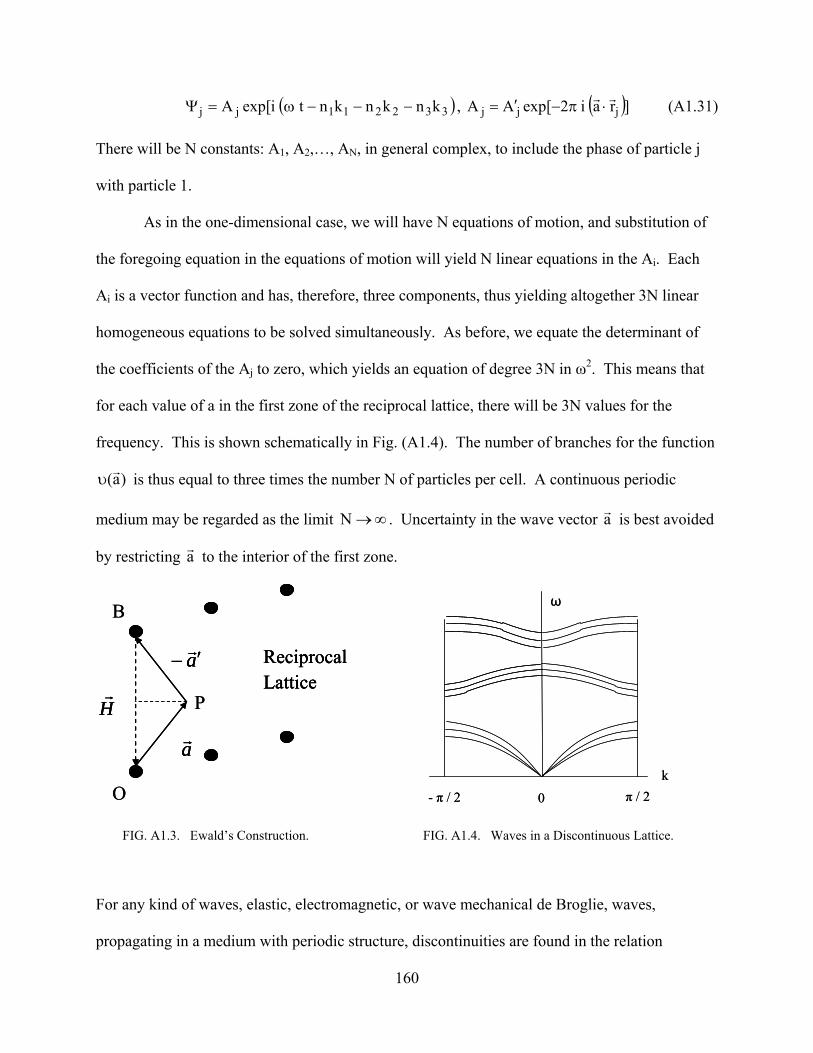
( ) 332211jj knknkntiexp[A −−−ω=Ψ , ( )]rai2 jexp[AA jjrr⋅π′ −= (A1.31)
There will be N constants: A1, A2,…, AN, in general complex, to include the phase of particle j
.
uation in the equations of motion will yield N linear equations in the Ai. Each
i is a
with particle 1
As in the one-dimensional case, we will have N equations of motion, and substitution of
the foregoing eq
A vector function and has, therefore, three components, thus yielding altogether 3N linear
homogeneous equations to be solved simultaneously. As before, we equate the determinant of
the coefficients of the Aj to zero, which yields an equation of degree 3N in ω2. This means that
for each value of a in the first zone of the reciprocal lattice, there will be 3N values for the
frequency. This is shown schematically in Fig. (A1.4). The number of branches for the function
)a(υ is thus equal to three times the number N of particles per cell. A continuous periodic
medium may be regarded as the limit
r
∞→N . Uncertainty in the wave vector a is best avoided
stricting a to the interior of the first zone.
r
by rer
a′−r
Hr
ar
ReciprocalLattice
O
P
B
a′−r
Hr
ar
ReciprocalLattice
a′−r
Hr
ar
ω
π / 2- π / 2 0
k
ωB
ReciprocalLattice
O
P
π / 2- π / 2 0
k
FIG. A1.3. Ewald’s Construction. FIG. A1.4. Waves in a Discontinuous Lattice.
For any kind of waves, elastic, electromagnetic, or wave mechanical de Broglie, waves,
propagating in a medium with periodic structure, discontinuities are found in the relation
160
ar (a vector of length λ= /1arbetween the frequency υ and the wave vector and pointing in the
inates
hese
ure may
direction of propagation). These discontinuities are obtained whenever the vector ar term
on a plane that is a perpendicular bisector of one of the vectors of the reciprocal lattice. T
planes play the same role for all waves, whatever their particular nat be. For instance, in
electromagnetic waves, the discontinuities in )a(rυ are directly responsible for the selective
reflection of X-rays (Bragg-Laue spots). This general property is the reason for choosing these
special planes as limits of the zones defined earlier, and the zone structure, in a given crystal
lattice, is the same for all waves. These zones generally known in the literature as Brillo
zones.
Elastic vibrations, for instance, are propagated through a crystal lattice as elastic wave
Their properties result from the earlier analyses and their generalizations in three dimensions.
Assumi
are uin
s.
ng N atoms per lattice cell (lattice with basis), the best representation of the waves is
obtained by restricting the ar vector to the first zone. Each ar vector yields 3N different wave
motions, of which three are of the acoustic type and 3(N-1) of the optical type, as Fig. (A1.4)
shows schematically for the case N=3. The three acoustic waves correspond to the well-know
waves in an isotropic solid: se vibrations. In an ideal
continuous anisotropic medium, three vibrations at right angles to each other are obtained, non
of which is exactly longitudinal, or transverse. In the crystal lattice with discontinuous structure,
there are still three different acoustic waves for each a
n
one longitudinal and two transver
e
r vector, but their properties are m
complicated than for a continuous medium. We may, for the sake of visualization, call the
waves longitudinal, l, and transverse, t1, t2, but these names do not correspond exactly to the
properties of waves in a lattice structure.
The hexagonal lattice, although it contains only one type of atom, yet it is a lattice w
uch more
ith
161
basis, and yields three acoustic branches, and three branches of higher frequency, which may
called optical. A real monatomic crystal l
be
attice, such as the face- or body-centered cubic
structure, is one without basis, and contains only one atom per cell. It yields only three acoustic
branches and no optical branches.
162

Appendix 2
Transport of Heat and Electricity in Solids
A2.1 Crystalline Solids
Condensed matter exists in many different forms: organic, inorganic, liquids, crystalline
solids, amorphous solids, ionic conductors, covalent conductors, etc. However, the materials
presently employed in thermoelectric devices are inorganic semiconductor crystalline solids. We
suppose, therefore, that such solid bodies consist of one or more crystals; the atoms in each of
which are regularly arranged in the form of a lattice. The crystal lattice is a framework along
which the carriers of electric charge and thermal energy move. The vibrations of the lattice
provide one of the principal mechanisms of heat transfer. There is a wide variety of crystal
structures that may be assumed by an element or compound. The particular structure that is
observed is governed, to a certain extent, by the nature of the binding between the atoms. There
are four types of atomic bonds, namely, the ionic, covalent, metallic and van der Waals bonds.
The simplest bonds arise from coulombic attraction between ionized atoms that bear charges of
opposite sign. Sodium chloride constitutes the most typical example of an ionic bond. In this
compound, each of the sodium atoms loses one electron, to become positively charged. The
chlorine atoms become negatively charged, as each takes up an electron. The arrangement in the
sodium chloride is stable when each positive or negative ion is surrounded symmetrically by six
ions of the opposite sign. If all the atoms were identical, we would have a simple cubic lattice.
Taking account of the two different types of atom, we see that the lattice is of the face centered
cubic type. We note that a repulsive force that becomes very strong as the spacing becomes
smaller opposes the coulombic attraction between oppositely charged ions. At equilibrium
163

atomic spacing, the attractive and repulsive forces balance. If one examines the periodic table,
one notices that Group IV contains the elements silicon and germanium, which, like one form of
carbon and gray tin, have a diamond structure. In this structure, each atom shares the four
electrons in its outer shell with its four nearest neighbors. Thus the binding between each pair of
atoms involves two electrons, and is termed covalent. Unlike an ionic bond, a covalent bond is
strongly directional, so that, in the diamond structure, the four nearest neighbors of each atom lie
at the corners of a tetrahedron. In covalently bonded crystals, the electrons are concentrated near
the lines that join neighboring atoms, whereas in ionic crystals, the electrons form almost
spherical clouds around the negative ions. The atoms to the left of Group IV are termed
electropositive, because they tend to donate, or give up, electrons, thereby becoming positive
ions. Likewise, the atoms to the right of Group IV are termed electronegative, because they tend
to accept, or take, electrons. The alkali halides exemplify the principle that compounds between
strongly electropositive and strongly electronegative elements contain ionic bonds, whereas
when the electronegativity difference is small, covalent bonding predominates. The nature of the
bonding has a considerable bearing on the transport properties of solids.
In a metallic bond, as in a covalent bond, atoms are bound together by shared electrons.
In this case, however, the participating electrons are less influenced by s-p hybridization, and the
electron density is more uniform. The number of nearest neighbors is no longer determined by
considerations of valence, and many metals form structures in which the atoms are as near to one
another as possible. These are face centered cubic and close packed hexagonal structures.
The fourth type of bond is much weaker than the aforementioned three ones. This bond
is particularly important in condensed inert gases. It is also of some significance in certain
thermoelectric materials, notably those that have layered structures.
164

A2.2 Heat Conduction by the Lattice
The fact that metals are good conductors of heat can be attributed to the transport of heat
by the charge carriers. Of course, heat can also be conducted through electrical insulators. The
thermal conductivity of diamond, for example, exceeds that of any metal. It is, in fact, the
transfer of vibrational energy, from one atom to the next, that constitutes this process.
The atoms in a crystal do not vibrate independently. Rather, the vibrations are such that
elastic waves continually pass backward and forward through the crystal. An increase in
temperature should lead to an increase in the amplitude of a given wave, as well as redistribution
of the relative amplitudes for different wavelengths. This concept was used by DebyeA4 to
determine the specific heat of a solid. Although Debye’s theory is now known to have
shortcomings, it is still regarded as a first step toward the complete description of the thermal
properties of solids.
Debye represented the crystal as an elastic continuum. When boundary conditions are
imposed, only certain modes of vibration are possible. For example, if the surfaces of the crystal
are to correspond to nodes, this condition can be realized only for waves in a particular direction,
if they have particular wavelengths. In a true continuum, the total number of modes of vibration
would be infinite. Debye showed that the discrete nature of atoms sets a lower limit to the
wavelength. Therefore, one should take account of only the 3N modes of lowest frequency,
where N is the number of atoms per unit volume. This restriction on the number of vibrational
modes gives a result at high temperatures that is consistent with the Dulong and Petit law, which
states that the specific heat per atom is equal to 3kB, where kB is the Boltzmann constant. The
number of modes, dw, per unit volume, that have frequencies between υ and υ+dυ, is given by
165

υπ
= dvυ2dw 3
2 (A2.2.1)
where v is an appropriate average value for the speed of sound. In a simple continuum, the speed
of sound is independent of frequency, but, even in an isotropic solid, it will be different for
longitudinal and transverse waves.
The plot of frequency, υ, against wave number, a = 1/λ, or the dispersion curve, is linear
through the origin for a continuum, but becomes nonlinear at high frequencies in real materials.
If more than one atom is associated with each lattice point, the dispersion curve also has separate
branches that have one or more optical branches to each acoustic branch. In three dimensions,
there will be three acoustic branches (one for the longitudinal vibrations and one for each
polarization of the transverse vibrations) and 3(n-1) optical branches, where n is the number of
atoms per primitive cell. The group velocity, determined by the slope of the dispersion curve, is
of particular interest, because it is related to the rate of energy transport. It clearly depends on
frequency or wave number, and also differs considerably for acoustic and optical modes.
The limit of 3N on the number of modes means that there is an upper frequency limit, or
cut off frequency, υD, which may be obtained by integrating Eq. (A2.2.1). υD is given by
∫∫υ
υ−υ
π=
D
D3
2N
0d
vυ2dw
and therefore
( )( )3D
3D3
Dυ
Dυ
33
N0 υυ
v32υ
v32w −−
π=
π=
−
thus
166
3D3 υv3
π4N = or vπ4N3υ 3
1
D ⎟⎠⎞
⎜⎝⎛= (A2.2.2)
The above equation forms the basis for the definition of the so-called Debye temperature, which
is
B
DD k
hυθ = (A2.2.3)
Debye’s success in explaining the general behavior of specific heat as a function of temperature
was due to his use of quantum theory. He showed that the average energy, W, in a mode of
frequency, υ, is
1
B1
TkhυexphυW
−
⎥⎦
⎤⎢⎣
⎡−⎟⎟⎠
⎞⎜⎜⎝
⎛= (A2.2.4)
where h is Planck’s constant. With the frequency limit set by Eq. (A2.2.2), Eqs. (A2.2.1) and
(A2.2.4) allow one to determine the internal energy of the crystal. Then, by differentiating the
internal energy with respect to temperature, the specific heat at constant volume is
( )
dx1(x)exp
(x)expxθTNk9c
/TDθ
02
43
DBv ∫ −⎟⎟
⎠
⎞⎜⎜⎝
⎛= (A2.2.5)
Debye’s theory has been so successful that it is usual to fit Eq. (A2.2.5) to the experimental data,
by regarding θD as a temperature-dependent parameter.
The relative accuracy of Eq. (A2.2.5) does not indicate that Debye’s theory gives a
particularly good description of the vibrations in a real crystal. Therefore, specific heat studies
are not a good way to determine the distribution of the vibrational modes. The vibrational
spectra can, however, be found by the neutron scattering method of BrockhouseA1 and others.
The first requirement of any theory of lattice heat transport is that it should explain the
observation of EuckenA6 that, for pure dielectric crystals, thermal conductivity varies inversely
167

with absolute temperature. Eucken’s rule has been confirmed for many materials, provided that
the temperature is not much less than θD.
DebyeA5 attempted to use his continuum model to explain Eucken’s 1/T law, but found
out that the thermal conductivity is infinite. It is only by taking account of the anharmonic
nature of the forces in real crystals that thermal conductivity takes on finite values. If an atom is
displaced from its equilibrium position by an infinitesimal amount, the restoring force is
proportional to the displacement, i.e., it is harmonic. As the displacement becomes larger, the
expression for the restoring force includes higher order terms. Then the force is partially
anharmonic. In effect, the elastic constants of the substance vary from point to point according
to the local displacements of the atoms. Variations in either the density or the elastic properties
are responsible for scattering the vibrational waves and, thus, for limiting the value of thermal
conductivity.
PeierlsA8 showed how the anharmonicity of the lattice vibrations could be taken into
account. He introduced the concept of phonon wave packets that arise from the quantization of
vibrational waves. One refers to the wave packets simply as phonons, and they may be regarded
as the energy carriers that are responsible for heat conduction by the lattice. A limit on thermal
conductivity is set by phonon collisions that do not conserve momentum. One may draw on the
kinetic theory of gases to express the lattice thermal conductivity, κL, in terms of the mean free
path of the phonons. Thus,
tvL vc31κ l= (A2.2.6)
where the specific heat, Cv, is defined for unit volume, v is the speed of sound and lt is the mean
free path length.
In pure crystals at high temperatures, phonons are scattered predominantly by other
168

phonons. The most important processes involve three phonons and can be of two kinds. In the
normal, or N-processes, both energy and momentum are conserved. In Umklapp or U-processes,
momentum, or more strictly, wave number, is not conserved. The N-processes lead to a
redistribution of phonons, but no thermal resistance to first order. Therefore, the U-processes
directly control high-temperature thermal conductivity.
The difference between the N- and U-processes is indicated in Fig. (A2.2.1). Two-
dimensional representations of wave-vector space are shown: the squares correspond to all
values of the phonon wave vector set by the frequency limit, υD. The maximum x or y
component of the wave vector is equal to half the side of the square. The region of wave-vector
space that contains the allowed values for the wave vector is called the Brillouin zone.
In the N-process, two phonons of wave vector, 1qr and 2q
r , interact to form a third
phonon of wave vector, , such that 3qr
321 qqq rrr=+ (A2.2.7)
On the other hand, in the U-process, the sum of the wave vectors, 1qr
and , would produce a
resultant outside the Brillouin zone, if Eq. (A2.2.7) were applied. Thus one subtracts the vector,
, the reciprocal lattice vector, to produce a resultant wave vector,
2qr
Gr
3qr , that lies within the
allowed zone. The rule for the conservation of a wave vector for the U-process is
Gqqq 321rrrr
+=+ (A2.2.8)
Peierls showed that the increasing probability of U-processes with a rise in temperature
explains Eucken’s 1/T law. However, at low temperatures, it becomes exceedingly difficult for
any U-processes to occur. When T << θD, there are virtually no phonons where wave vectors are
comparable to half-width of the Brillouin zone, and very few with even half that value. The only
169

real possibility for finding a U-process is when two phonons have wave vectors marginally
greater than a quarter of the Brillouin zone width, provided that they happen to have, more or
less, the same direction. The number of such phonons is proportional to exp(-θD/2T), so one
might expect that lt at low temperatures is proportional to [exp(-θD/aT)]-1, where a ≈ 2. The
exponential variation of lt should have a major influence on the dependence of thermal
conductivity on temperature.
Although there is no doubt that the inverse temperature dependence of thermal
conductivity, when T > θD, will always change to an exponential dependence for T << θD in a
sufficiently pure and perfect large crystal. In practice, it is often difficult to observe such
behavior. It is usually found that scattering by all kinds of internal defects, and by the external
crystal boundaries, masks phonon-phonon scattering at low temperatures. In fact, we can
sometimes take advantage of these other phonon-scattering processes to improve thermoelectric
materials. Therefore, it is important for one to consider lattice conductivity in less than perfect
crystals.
1qr 2qr
3qr
qx
qy
1qr 2qr
3qr
qx
qy
1qr2qr
3qr
qx
qy
Gr
1qr2qr
3qr
qx
qy
Gr
(a) (b)
FIG. A2.2.1. Two-dimensional representation of: (a) N-process and (b) U-process.
170
A2.3 Scattering of Phonons by Defects
As the temperature of a dielectric crystal is lowered, its thermal conductivity rises to a
maximum value, and then falls so as to approach zero at 0 K. At the lowest temperatures,
thermal conductivity is proportional to T3, which is the same variation with temperature as that
of specific heat. This implies that lt must have reached a limiting value. CasimirA3 showed that
this value is comparable to the dimensions of the crystal, and can be attributed to the scattering
by phonons at the crystal boundaries. In a polycrystalline sample, one expects that the maximum
free path length of the phonons is set by the grain size. It is even found that amorphous solids
behave as if heat conduction arises from phonons whose free path lengths are comparable to the
inter-atomic spacing. One might expect boundary scattering to have an effect on the lattice
conductivity of crystalline materials only when the temperature is low enough for lt of phonons
to be very large.
Now, one discusses scattering by the various point defects that are found in real crystals.
Examples of such defects are the local variations of elasticity and density, that occur in solid
solutions between isomorphous crystals, e.g., silicon-germanium alloys, or in an element or
compound that contains foreign impurities or vacancies. It is even possible to observe scattering
of phonons due to the density variations associated with the different isotopes in naturally
occurring elements.
The treatment of the scattering of phonons by point defects presents us with a difficulty.
The relaxation time, , for this form of scattering should be proportional to 1/ υ4. This means
that point defect scattering does not have a significant effect on low-frequency phonons. The
thermal conductivity at low temperatures then becomes exceedingly large because U-processes
also have little effect in this region. That this phenomenon does not occur can be explained if
Iτ
171
one takes account of the redistribution of phonons by N-processes into modes for which the
scattering is stronger.
CallawayA2 developed a satisfactory method of including N-processes. In Callaway’s
treatment, one uses the relaxation time, τ, rather than lt; the two quantities are related through
. The basic principle is that non-momentum-conserving processes cause the perturbed
phonons to relax toward equilibrium distribution, whereas N-processes cause them to relax
toward a non-equilibrium distribution. If all of the scattering processes were non-momentum-
conserving, the overall relaxation time could be obtained simply as the reciprocal of the sum of
the reciprocal relaxation times of the individual processes. Callaway successfully obtained a
multiplying factor that corrects for the momentum-conserving behavior of N-processes.
vτt =l
Suppose that there are two different relaxation times, τR, for the processes that change the
momentum, and τN for the N-processes. The rate at which the phonon distribution function, N,
changes through the various scattering effects is
N
N
R
o
scatter
NNNNdtdN
τ−
+τ−
=⎟⎠⎞
⎜⎝⎛ (A2.3.1)
where No is the equilibrium distribution function and NN is the distribution function to which N-
processes on their own would lead. At the same time, the temperature gradient, ∇T, changes the
distribution function according to
TNTv
diffusiondtdN
∂∂
∇−=⎟⎠⎞
⎜⎝⎛ rr (A2.3.2)
where is the sound velocity in the direction of the phonon wave vector, . Because the
diffusion and scattering processes must balance,
vr Lqr
0TNTv
τNN
τNN
N
N
R
o =∂∂
∇−−
+− rr (A2.3.3)
172
Now, the N-processes must lead to a distribution that carries momentum against the
temperature gradient. A suitable distribution is
1
B
LN 1
TkqωexpN
−
⎥⎥⎦
⎤
⎢⎢⎣
⎡−⎟⎟⎠
⎞⎜⎜⎝
⎛ ⋅−=
lrr
h (A2.3.4)
instead of the usual Bose-Einstein distribution function
1
Bo 1
TkexpN
−
⎥⎦
⎤⎢⎣
⎡−⎟⎟
⎠
⎞⎜⎜⎝
⎛ ω=
h (A2.3.5)
It is convenient to use the angular frequency, ω, which is equal to 2πυ, and π= 2hh .
In Eq. (A2.3.4), l is a constant vector in the direction of r
∇r
T, where lrr⋅Lq << ħω. In effect, Eq.
(A2.3.4) differs from Eq. (A2.3.5) in that the frequency, ω, is changed by hrr/qL l⋅ .
Consequently, one finds that
( )2B
LoN
1(x)exp(x)exp
TkqNN
−
⋅=−
lrr
(A2.3.6)
where x = ħω / k BT. Also
( )22
B 1)xexp()xexp(
TkTN
−
ω=
∂∂ h (A2.3.7)
so that
TN
ωTqNN L
oN ∂∂⋅
=−h
rrl (A2.3.8)
Substituting Eq. (A2.3.8) into Eq. (A2.3.3) gives
( ) 0TN
ωτTqT.v
τ1
τ1NN
N
L
NRo =
∂∂
⎥⎦
⎤⎢⎣
⎡ ⋅−∇−⎥
⎦
⎤⎢⎣
⎡+−
h
rrrr l (A2.3.9)
Because l should be proportional to the temperature gradient, one writes r
173
TβvT
2∇−=rhr
l (A2.3.10)
where β is a constant whose dimension is time. Also, using the Debye model to express v as
ω / qL, Eq. (A2.3.9) becomes
( ) 0TNT.v
τβ1
τ1
τ1NN
1
NNRo =
∂∂
∇−⎥⎦
⎤⎢⎣
⎡+⎥
⎦
⎤⎢⎣
⎡+−
− rr (A2.3.11)
This means that the behavior is exactly the same as it would be if there were an effective
relaxation time, τeff, given by
1
NC
1
NNReff111111
−−
⎥⎦
⎤⎢⎣
⎡τβ
+τ
=⎥⎦
⎤⎢⎣
⎡τβ
+⎥⎦
⎤⎢⎣
⎡τ
+τ
=τ
(A2.3.12)
Here, τC is the relaxation time that we would expect if the N-processes did not conserve wave
vector, because then we would merely add the reciprocal relaxation times for all of the scattering
processes. We thus see that τC must be multiplied by (1+β / τN) to yield τeff.
The constant, β, is found by using the fact that N-processes conserve the wave vector. In
other words,
∫ ∫ =−
=− 0dωq
τNN
v
ωπ4qdq
τNN
LN
N3
2
L3
LN
N rrr (A2.3.13)
Because NN-N = (NN-No) + (No-N) is proportional to (β-τeff)∂N/∂T, Eq. (A2.3.13) can be written
as
( )
0dx1)xexp(
)xexp(2
T/
0
42N
C
N
C
N
D
=−
ω⎥⎥⎦
⎤
⎢⎢⎣
⎡
τ
βτ−
ττ
−τβ∫
θ (A2.3.14)
Thus, we find that
174
( )
( )dx
1)xexp()xexp(x11
dx1)xexp(
)xexp(x
2
T/D
0
4
N
C
N
2
T/D
0
4
N
C
−⎥⎦
⎤⎢⎣
⎡ττ
−τ
−ττ
=β
∫∫
θ
θ
(A2.3.15)
The general determination of β is difficult, but Callaway showed that a simplification of
the expression is possible in certain cases. For example, if the scattering by the imperfections is
very strong, and the relaxation time τI << τN, it is valid to use the approximation, 1/τeff = 1/τI +
1/τN. Another approximation may be made at low temperatures for fairly pure crystals, when τI
>> τN and U-processes can be neglected. However, when we are dealing with thermoelectric
materials, the high temperature approximation used by ParrottA7 is of interest. The relaxation
times for both U- and N-processes are expected to be proportional to ω-2, whereas for point
defects, τI is proportional to ω-4. Suppose, then that the relaxation times are expressed as 1/τI =
Aω4, 1/τU = Bω2, 1/τN = Cω2, where A, B and C are constants for a given sample. Also, when T
>> θD, x << 1 for the whole phonon spectrum, so that x2exp(x) / (exp(x)-1)2 ≈ 1. Then it is
possible to obtain analytical solutions for the integrals involved in β and to express, κL, for the
crystal, with point imperfections, in terms of the value, κo, that would be found for a perfectly
pure crystal. The expression is
⎥⎥
⎦
⎤
⎢⎢
⎣
⎡
⎟⎟⎠
⎞⎜⎜⎝
⎛−−
+⎟⎟⎠
⎞⎜⎜⎝
⎛−+⎟
⎠⎞
⎜⎝⎛ +=
κκ
−−−−− 112
o
o42111
o
o
Ly
ytan3
yk5
)k1(yy
ytan1y
ytan9k5
1 (A2.3.16)
where ko, equal to C/B, is a measure of the relative strengths of the N- and U-processes. The
quantity, y, is defined by
1
o2
o
D29k5
1y−
⎟⎠⎞
⎜⎝⎛ +⎟⎟
⎠
⎞⎜⎜⎝
⎛ωω
= (A2.3.17)
where ωo is given by
175
Aωvκπ2
kωω
Do2
B2
D
o =⎟⎟⎠
⎞⎜⎜⎝
⎛ (A2.3.18)
The value of ko may be determined experimentally by measuring the thermal conductivity
of one pure crystal, and one that contains imperfections. Thereafter, the same value of ko can be
used for crystals with other concentrations of defects.
One notes that the approximations that hold strictly for T >> θD are often used with
reasonable success for the less stringent condition, T ≥ θD.
176

Appendix 3
Band Theory of Solids
A3.1 Energy Bands in Metals, Insulators and Semiconductors
In the classical free electron theory of metals, it was supposed that the atomic nuclei and
all, except the outer, electrons are in fixed positions, whereas the outer electrons form as “gas”
that can be described by the familiar kinetic theory. In particular, a mean thermal energy of
3kBT/2 was ascribed to each of the free electrons; the energy being distributed according to the
Maxwell-Boltzmann law.
Although the classical free-electron theory accounted for Ohm’s law, predicted the right
order of magnitude for the electrical resistivity and also explained the observed relationship
between the electrical and thermal conductivity in metals (the Wiedemann-Franz law), yet it
failed badly in certain other respects. A most obvious shortcoming was its prediction of a
substantial component of the specific heat from the electrons, whereas, at ordinary temperatures,
it is observed that the electronic specific heat is negligible. This and other failures of the
classical theory can be eliminated, however, if we take account of the fact that the free-electron
gas should obey Fermi-Dirac statistics rather than Maxwell-Boltzmann statistics. That is to say,
classical theory must be replaced by quantum theoryA9. The following are the rules that must be
complied with: (1) Electrons can have spin quantum numbers of +1/2 or -1/2 but are otherwise
indistinguishable from one another. (2) Electrons have discrete values for their energy and
momentum. (3) No more than one electron of a given spin can reside in one of these discrete
states (Pauli Exclusion Principle).
SommerfeldA9 showed that the number of permitted electronic states with energies in the
177

range from E to E + dE, per unit volume, is given by
( )3
2/12/3
hdEEm24dE)E(g π
= (A3.1.1)
where m is the mass of a free electron. The probability that a particular state will be filled is
given by the Fermi-Dirac distribution function
( )1
Bo 1
TkEexpEf
−
⎥⎦
⎤⎢⎣
⎡+⎟⎟
⎠
⎞⎜⎜⎝
⎛ ζ−= (A3.1.2)
where ζ is the Fermi energy, which has a value such that
(A3.1.3) ( ) ( ) ndEEgEf0
o∫∞
=
where n is the total number of free electrons per unit volume. At the absolute zero of
temperature, the Fermi energy has the value
3/22
o 8n3
m2h
⎟⎠⎞
⎜⎝⎛π
=ζ (A3.1.4)
All the states with E < ζo are filled with electrons, whereas all the states with E > ζo are empty.
This, of course, is in contrast to the result from classical theory that all electrons have zero
energy at 0 K. It should be noted that, at ordinary temperatures, ζ >> kBT for all metals, which
means that ζ ζo. ≅
Eq. (A3.1.4) shows that the value of the Fermi energy at the absolute zero of temperature
can become small if the free-electron concentration, n, is much less than is normally found in a
metal. It is then possible to achieve the condition, kBT >> ζo, at ordinary temperatures, whence
Eq. (A3.1.2) reduces to
( ) ⎟⎟⎠
⎞⎜⎜⎝
⎛ ζ−−=
TkEexpEf
Bo , kBT >> ζo (A3.1.5)
178
This is, in fact, the Maxwell-Boltzmann distribution function that is used in the classical kinetic
theory of gases. When n is small enough for Eq. (A3.1.5) to apply, the electron gas is said to be
nondegenerate. On the other hand, when n is so large that kBT << ζo, we have what is called
degenerate electron gas. It turns out that thermoelectric materials tend to lie between these two
extremes.
In a free-electron gas, the energy, E, varies as the square of the wave vector, kr
. This
clearly cannot be generally true for energy bands, although, close to the maxima and minima, the
bands are parabolic in shape. This means that, if we measure the energy and wave vector from
the band edge, then E k2, for small values of E and k. Thus, we may write ∝
*m8
khE 2
22
π= (A3.1.6)
which is the same expression as for a free-electron gas, except that the mass, m, of an electron
has been replaced by m*, known as the effective mass. It should be noted that the same effective
mass may be inserted into Eq. (A3.1.1) to yield a density of states, near the band maximum or
minimum, of
( ) ( )3
2/12/3
h
EdE*m24dEEg
π= (A3.1.7)
In these cases, the interaction between the electrons and the crystal lattice is fully taken into
account by using the effective mass.
The effective mass may be defined quite generally by the expression
2
2
2 dkEd1
*m1
h=
or (A3.1.8)
179
1
2
22
dkEd*m
−
⎟⎟⎠
⎞⎜⎜⎝
⎛= h
but it is only near band edges that Eqs. (A3.1.6) and (A3.1.7) can usefully be employed. Of
special interest is the situation near a band maximum, when d2E/dk2 becomes negative. This
means that the crystal behaves as if it contains negative carriers of negative mass, but it is
convenient to regard these as positive carriers of positive mass, known as positive holes (usually
just ‘holes’). It is this feature of band theory that explains why the values for the thermoelectric
and Hall coefficients are sometimes positive. When we are dealing with positive holes, the
energy, E, must be measured downwards from the band edge, if, for example, Eq. (A3.1.6) is to
be used. Also, the Fermi energy, ζ, must be measured downwards from the same band edge, and
the function, f(E), then represents the probability of a state being unoccupied by an electron, that
is, occupied by a hole.
Energy-band theory has been particularly successful in accounting for the difference
between metals, semiconductors and insulators. In a metal, the Fermi energy lies within one, or
more, of the allowed bands, and well away from the band edge. The density of electron states is
large in such a region, and the electrical conductivity is high in such a partly filled band. On the
other hand, in an electrical insulator, the Fermi level lies within a forbidden gap. The bands
below the gap are all completely full, so there are no free states into which electrons can move.
The bands above are completely empty, so they cannot contribute to the conduction either.
In fact, this last statement is not quite true except at the absolute zero of temperature. At
any temperature above 0 K, some electrons will be excited from the highest full band to the
lowest empty band, so that there will be a finite, albeit small, electrical conductivity. If the
energy gap, Eg, is small enough, substantial numbers of electrons in the upper band, and equal
180

numbers of holes in the lower band, will be excited in this way. The substance is then said to be
an intrinsic semiconductor.
It has been found possible to make a great many materials that are essentially insulators
in their pure state into electrical conductors, by adding impurities. Sometimes the impurities
give up electrons to the upper band and are said to be donors. Alternatively, the impurities may
take up electrons from the lower bands, so as to leave behind positive holes; such impurities are
called acceptors. In both cases, the states associated with the impurities usually lie very close to
the appropriate band edge, so that excitation is virtually complete at ordinary temperatures. The
substances in which the charge carriers originate from the addition of impurities are known as
extrinsic semiconductors.
Energy diagrams rather than band-structure diagrams are useful, when we have no
particular interest in the value of the wave vector. It will be observed that the upper and lower
allowed bands are called the conduction band and valence band, respectively.
The essential difference between an insulator and an intrinsic semiconductor is just the
width of the energy gap in terms of kBT. Thus, an insulator at ordinary temperatures may
become an intrinsic semiconductor at an elevated temperature. Likewise, as the temperature of
an extrinsic semiconductor is raised, the charge carriers excited across the energy gap will
eventually predominate over the carriers due to the impurities. When this happens, the extrinsic
semiconductor becomes intrinsic.
There are certain materials in which the valence and conduction bands just overlap one
another. They are called semimetals, and they do not differ substantially in their properties from
narrow-gap semiconductors. Their carrier concentration can, for example, be changed by adding
donor or acceptor impurities. This is in contrast with the situation in ordinary metals, in which
181

the changes of electrical resistivity, on adding impurities, are the result of a reduction in the free
path length, rather than the result of any alteration of the carrier concentration.
A3.2 Electron-Scattering Processes
The transport properties of a conductor depend not only on the concentration of the
charge carriers but also on their free path length between collisions. This would have an infinite
value if the electrons or holes were moving in a perfectly periodic potential, since they would
then never be scattered. However, in any real crystal, the free path length is limited by scattering
due to local distortions of the potential electronic function.
Transport coefficients can be derived from Boltzmann’s equation, and the scattering
processes can be described in terms of a relaxation time, τe. If the electron distribution function
is disturbed from its equilibrium value, fo, to f, where |f-fo| << fo, the system relaxes according to
the equation
( ) ( ) ( )e
o
scatter
EfEfdt
Edfτ−
−=⎟⎠⎞
⎜⎝⎛ (A3.2.1)
The relaxation time can, hopefully, be expressed in the form
(A3.2.2) roe Eτ=τ
where τo and r are constants. There may well be several scattering processes, with relaxation
times, τe1, τe2, …, that should all be taken into account, whereupon
...111
2e1ee τ+
τ=
τ (A3.2.3)
but it is usually supposed that one process predominates.
In a pure and perfect crystal, the carriers are scattered by the thermal vibrations of the
crystal lattice. Both the acoustic and the optical modes can upset the periodicity of the potential.
182

The acoustic modes perturb the lattice potential in two ways. The local changes of lattice
parameter directly influence the energy-band structure, leading to so-called deformation
potentials. Alternatively, if the atoms in the crystal are partly ionized, piezoelectric potentials
result from their displacement. It is usually assumed that the deformation-potential scattering is
much stronger than the piezoelectric scattering.
Similarly, optical vibrations can cause scattering in more or less the same two ways. In
this case, it is usual to refer to the mechanisms as nonpolar and polar. The polar process that
creates dipole moments, which vary in time and space, may completely outweigh nonpolar
processes.
When electrons and holes with a given energy are located at different points in the
Brillouin zone, as in a multivalley semiconductor, lattice scattering may involve large changes of
wave vector (intervalley scattering), as well as small changes (intravalley scattering). The two
processes have different effects at low temperatures, but at high temperatures, when there are
substantial numbers of phonons with large wave vectors, intervalley scattering becomes similar
to intravalley scattering.
A number of other scattering processes become possible in imperfect and impure crystals.
Impurity atoms act as scattering centers, particularly if they are ionized. Crystal defects, such as
dislocations, can also produce a significant effect. Often, mixed crystals or solid solutions are
used in thermoelectric materials, in which case alloy scattering can become important. Finally,
one should remember that the charge carriers can scatter one another, though it is doubtful that
carrier-carrier scattering is significant at the concentrations in which we are interested.
183

References
1. H.B. Callen, Phys. Rev. 73, 1349 (1948). 2. A.F. Ioffe, Semiconductor Thermoelements and Thermoelectric Cooling, Infosearch,
London, 136 (1957). 3. M. Shtenbeck and P.I. Baranskii, Zhur. Tekh. Fiz. 26, 683 (1956). 4. J.W. Christian, J.P. Jan, W.B. Pearson and I.M. Templeton, Canad. J. Phys. 36, 627 (1958). 5. G. Borelius, W.H. Keesom, C.H. Johansson and J.O. Linde, Proc. Acad. Sci. Amst. 35, 10
(1932). 6. E. Altenkirch, Phys. Zeits. 10, 560 (1909). 7. E. Altenkirch, Phys. Zeits. 12, 920 (1911). 8. A.F. Ioffe, Semiconductor Thermoelements and Thermoelectric Cooling, Infosearch,
London, 111 (1957). 9. A.F. Ioffe, Semiconductor Thermoelements and Thermoelectric Cooling, Infosearch,
London, 36 (1957). 10. P. Debye, Ann. Phys. 39, 789 (1912). 11. B.N. Brockhouse, Phys. Rev. Lett. 2, 256 (1959). 12. A. Eucken, Ann. Phys. 34, 185 (1911). 13. P. Debye, Vorträge über die kinetische Theorie, Teubner (1914). 14. R.E. Peierls, Ann. Phys. 3, 1055 (1929). 15. H.B.G. Casimir, Physica 5, 495 (1938). 16. J. Callaway, Phys. Rev. 113, 1046 (1959). 17. J.E. Parrott, Proc. Phys. Soc. 81, 726 (1963). 18. G. Leibfried and E. Schlömann, Nachr. Akad. Wiss., Göttingen, Kl. 2 Math-Physik 2, 71
(1954). 19. J.S. Dugdale and D.K.C. MacDonald, Phys. Rev. 98, 1751 (1955). 20. R.W. Keyes, Phys. Rev. 115, 564 (1959). 21. A.W. Lawson, J. Phys. Chem. Solids 3, 154 (1957). 22. H.J. Goldsmid and R.W. Douglas, Br. J. Appl. Phys. 5, 386, 458 (1954). 23. A.V. Ioffe and A.F. Ioffe, Dokl. Akad. Nauk. SSSR 97, 821 (1954). 24. A.F. Ioffe, S.V. Airapetyants, A.V. Ioffe, N.V. Kolomoets and L.S. Stil’bans, Dokl. Akad.
Nauk. SSSR 106, 981 (1956). 25. S.V. Airapetyants, B.A. Efimova, T.S. Stavitskaya, L.S. Stil’bans, L.M. Sysoeva, Zh. Tekh.
Fiz. 27, 2167 (1957). 26. F.D. Rosi, Solid-State Electron. 11, 833 (1968). 27. P.G. Klemens, Phys. Rev. 119, 507 (1960). 28. J.R. Drabble and H.J. Goldsmid, Thermal Conduction in Semiconductors, Pergamon,
Oxford (1961). 29. A. Sommerfeld, Z. Phys. 47, 1, 43 (1928). 30. G.A. Slack, In CRC Handbook of Thermoelectrics, D.M. Rowe, Ed., CRC Press, Boca
Raton, FL, 407-440 (1995). 31. G.A. Slack, In Solid State Physics, Vol. 34, H. Ehrenreich, F. Seitz and D. Turnbull, Eds.,
Academic Press, New York, 1 (1979). 32. N.F. Mott and H. Jones, The Theory of the Properties of Metals and Alloys, Dover
Publications, New York (1958).
184

33. D.Y. Chung, L. Kordanidis, K.S. Choi and M.G. Kanatzidis, Bull. Kor. Chem. Soc. 19, 1283-1293 (1998).
34. M.G. Kanatzidis and F.J. DiSalvo, ONR Quart. Rev. XLVII, 14-22 (1996). 35. J.F. Meng, D.A. Polvani, C.D.W. Jones, F.J. DiSalvo, Y. Fei and J.V. Badding, Chem. Mat.
12(1), 197-201 (2000). 36. K.J. Proctor, K.A. Regan, A Littman and F.J. DiSalvo, J. Alloys Compounds 292, 124-128
(1999). 37. C.D.W. Jones, K.A. Regan and F.J. DiSalvo, Phys. Rev. B60, 5282-5286 (1999). 38. C.M. Bhandari, In CRC Handbook of Thermoelectrics, D.M. Rowe, Ed., CRC Press, Boca
Raton, FL, 27-42 (1995). 39. L.D. Hicks and M.S. Dresselhaus, Phys. Rev. B47, 12727-12731 (1993). 40. P. Larson, S.D. Mahanti and M.G. Kanatzidis, Phys. Rev. B61, 8162-8171 (2000). 41. G. Mahan, B. Sales and J. Sharp, Phys. Today 50, 42 (1997). 42. M.S. Dresselhaus, G. Dresselhaus, X. Sun, Z. Zhang, S.B. Cronin, T. Koga, J.Y. Ying and
G. Chen, Thermophys. Eng. 3, 89-100 (1999). 43. G. Chen, J. Heat Transfer-Trans. ASME 119, 220-229 (1997). 44. R. Venkatasubramanian, T. Colpitts, B. O’Quinn, S. Liu, N. El-Masry and M. Lamvik,
Appl. Phys. Lett. 75, 1104-1106 (1999). 45. G.D. Mahan and J.O. Sofo, Proc. Natl. Acad. Sci. USA 93, 7436-7439 (1996). 46. K.J. Proctor, C.D.W. Jones and F.J. DiSalvo, J. Phys. Chem. Solids 60, 663-671 (1999). 47. T.M. Tritt, Science 272, 1276-1277 (1996). 48. D.M. Rowe, Renew. Energ. 16, 1-4 (1999). 49. R. Venkatasubramanian, T. Colpitts, E. Watko, M. Lamvik and N. El-Masry, J. Cryst.
Growth 170, 817-821 (1997). 50. D.C. Johnson, Curr. Opin. Solid State Mat. 3, 159-167 (1998). 51. R.E. Treece, E.G. Gillan and R.B. Kaner, Comment Inorg. Chem. 16, 313-337 (1995). 52. I.P. Parkin, Chem. Soc. Rev. 25, 199 (1996). 53. W.S. Sheldrick and M. Wachhold, Coord. Chem. Rev. 176, 211-322 (1998). 54. D. Elwell and H.J. Scheel, Crystal Growth from High-Temperature Solutions, Academic
Press, New York (1975). 55. H.J. Scheel, J. Cryst. Growth 24/25, 669 (1974). 56. R. Sanjines, H. Berger and F. Levy, Mat. Res. Bull. 23, 549 (1988). 57. R.W. Garner and W.B. White, J. Crystal Growth 7, 343 (1970). 58. B.C. Sales, Curr. Opin. Solid State Mat. 2, 284-289 (1997). 59. G.S. Nolas, G.A. Slack, D.T. Morelli, T.M. Tritt and A.C. Ehrlich, J. Appl. Phys. 79,
4002-4008 (1996). 60. G.S. Nolas, J.L. Cohn, G.A. Slack and S.B. Schujman, Appl. Phys. Lett. 73, 178-180
(1998). 61. G.S. Nolas, T.J.R. Weakley and J.L. Cohn, Chem. Mat. 11, 2470-2473 (1999). 62. B.C. Sales, B.C. Chakoumakos, D. Mandrus and J.W. Sharp, J. Solid State Chem. 146,
528-532 (1999). 63. M.G. Kanatzidis and A. Sutorik, Prog. In Inorg. Chem. 43, 151-265 (1995). 64. S. Sportouch, M. Bastea, P. Brazis, J. Ireland, C.R. Kannewurf, C. Uher and M.G.
Kanatzidis (1998). In “New Materials for Small Scale Thermoelectric Refrigeration and Power Generation Applications,” Vol. 545 (T.M. Tritt, M.G. Kanatzidis, G. Mahan and H.B. Lyon, Jr., Eds.), pp.123-130. Proceedings of the 1998 Materials Research Society.
185

65. A.V. Morozkin, Y.D. Seropegin, V.K. Portnoy, I.A. Sviridov and A.V. Leonov, Mat. Res. Bull. 33, 903-908 (1998).
66. K. Saito, K. Sugiyama and K. Hiraga, Phil. Mag. Lett. 80, 73-78 (2000). 67. H.X. Sui, X.Z. Li and K.H. Kuo, Phil. Mag. Lett. 79, 181-185 (1999). 68. X.Z. Liao, H.X. Sui and K.H. Kuo, Phil. Mag. A 78, 143-156 (1998). 69. G.S. Nolas, J. Sharp and H.J. Goldsmid, Thermoelectrics: Basic Principles and New
Materials Developments, Springer-Verlag, Berlin Heidelberg New York, 39-42 (2001). 70. G.S. Nolas, J. Sharp and H.J. Goldsmid, Thermoelectrics: Basic Principles and New
Materials Developments, Springer-Verlag, Berlin Heidelberg New York, 63 (2001). 71. A.F. Ioffe, Semiconductor Thermoelements and Thermoelectric Cooling, Infosearch Ltd.,
London, 29 (1957). 72. H.J. Goldsmid, Thermoelectric Refrigeration, Plenum Press, New York, 37, 67 (1964). 73. H.J. Goldsmid, Thermoelectric Refrigeration, Plenum Press, New York, 35 (1964). 74. H.J. Goldsmid, Thermoelectric Refrigeration, Plenum Press, New York, 132 (1964). 75. E.S. Rittner, J. Appl. Phys. 30(5), 702-707 (1959). 76. E.S. Rittner and G.F. Neumark, J. Appl. Phys. 34(7), 2071-2077 (1963). 77. F.J. Donahoe, Elec. Eng. 79, 488 (1960). 78. P.J. Price, Phys. Rev. 104, 1223 (1956). 79. H. Littman and B. Davidson, J. Appl. Phys. 32, 217 (1961). 80. E.S. Rittner, J. Appl. Phys. 33, 2654 (1962). 81. R. Simon, J. Appl. Phys. 33, 1830 (1962). 82. C. Wood, Rep. Prog. Phys. 51, American Institute Phys., New York, 459-539 (1988). 83. E.S. Rittner and G.F. Neumark, J. Appl. Phys. 34, 2071 (1959). 84. P.R. Aigrain in “Thermoelectricity,” P.H. Egli, Ed., John Wiley & Sons, Inc., New York
and London, 185 (1960). 85. Y.M. Lin, X. Sun and M.S. Dresselhaus, Phys. Rev. B62(7), 4610-4623 (2000). 86. H.J. Goldsmid, Thermoelectrics Handbook / Macro to Nano, D.M. Rowe, Ed., CRC,
Taylor & Francis, 10-1 – 10-10 (2006). 87. D.G. Cahill, S.K. Watson and R.O. Pohl, Phys. Rev. B46, 6131 (1992). 88. G.A. Slack and M.A. Hussain, J. Appl. Phys. 70, 2694 (1991).
Appendix References
A1. B.N. Brockhouse, Phys. Rev. Lett. 2, 256 (1959). A2. J. Callaway, Phys. Rev. 113, 1046 (1959). A3. H.B.G. Casimir, Physica 5, 495 (1938). A4. P. Debye, Ann. Phys. 39, 789 (1912). A5. P. Debye, Vorträge über die kinetische Theorie, Teubner (1914). A6. A. Eucken, Ann. Phys. 34, 185 (1911). A7. J.E. Parrott, Proc. Phys. Soc. 81, 726 (1963). A8. R.E. Peierls, Ann. Phys. 3, 1055 (1929). A9. A. Sommerfeld, Z. Phys. 47, 1, 43 (1928).
186