Embed Size (px)
Citation preview
THEORY AND SIMULATION OF SUBWAVELENGTH HIGH CONTRAST
GRATINGS AND THEIR APPLICATIONS IN VERTICAL-CAVITY
SURFACE-EMITTING LASER DEVICES
THESIS
Submitted in partial fulfillment of the requirements
for the degree of Master of Science in Electrical and Computer Engineering
in the Graduate College of the
University of Illinois at Urbana-Champaign, 2011
Urbana, Illinois
Adviser:
Professor Kent D. Choquette
BY
STEPHEN NICHOLAS BROWN
ii
Abstract
This work intends to fully explore the qualities and applications of subwavelength gratings.
Subwavelength gratings are diffraction gratings with physical dimensions less than the wavelength of
incident light. It has been found that by tailoring specific dimension parameters, a number of different
reflection profiles can be attained by these structures including high reflectivity or low reflectivity with
broad and narrow spectral responses. In the course of this thesis the physical basis for this phenomenon
will be presented as well as a mathematical derivation. After discussion of the mechanics of the reflection
behavior, the methods used in modeling subwavelength gratings and designing them for specific
functions will be explored. Following this, the fundamentals of vertical-cavity surface-emitting lasers
(VCSELs) will be discussed, and the applications of subwavelength gratings when used with these lasers
will follow. Several devices, both theoretical proposals and fabricated examples, will be presented in
addition to the available performance measurements. Finally, the fabrication challenges that restrict
subwavelength gratings from adoption as standard components in VCSEL design will be considered with
regard to ongoing fabrication research.

iii
Acknowledgments
I would like to take this opportunity to thank the people who have made it possible for me to
reach this point in my academic career. First I would like to thank my adviser, Professor Kent Choquette,
who has encouraged and educated me more than I would have thought possible in just over a year. I
would also like to thank the members of the Photonic Device Research Group, whose experience and
knowledge has helped me on many occasions. In particular I would like to thank Josh Sulkin and Hailee
Jeong for their help and instruction in the clean room. I would also like to give a special thanks to Meng
Peun Tan for his assistance in fabricating the VCSEL used in this work.
Finally, my thanks to my friends and family: to my parents, whose love and support through my
whole life has given me the passion to pursue my education; to my brother and sister, on whose
encouragement and support I’ve relied; and also to Tara, who is largely responsible for my seeking out
and getting to this level in higher education.
iv
Table of Contents
CHAPTER 1 INTRODUCTION ................................................................................................................ 1
1.1 Background and Motivation ..................................................................................................... 1
1.2 Thesis Scope ............................................................................................................................ 3
1.3 References ................................................................................................................................ 4
CHAPTER 2 SUBWAVELENGTH GRATINGS ...................................................................................... 6
2.1 Theory of Operation ................................................................................................................. 6
2.2 Simulation Methods ............................................................................................................... 12
2.3 Grating Design Methodology ................................................................................................. 15
2.4 References .............................................................................................................................. 18
CHAPTER 3 APPLICATIONS WITH VCSELS ..................................................................................... 20
3.1 Vertical-Cavity Surface-Emitting Lasers ............................................................................... 20
3.2 VCSEL Devices with Subwavelength Gratings ..................................................................... 23
3.2.1 VCSEL with a Subwavelength Grating Mirror ............................................................... 23
3.2.2 Tunable VCSEL .............................................................................................................. 27
3.2.3 Multiwavelength VCSEL Arrays .................................................................................... 29
3.2.4 Lateral Coupling VCSEL ................................................................................................ 30
3.3 Fabrication ............................................................................................................................. 34
3.4 References .............................................................................................................................. 35
CHAPTER 4 CONCLUSION ................................................................................................................... 37
4.1 Summary ................................................................................................................................ 37
4.2 Future Work ........................................................................................................................... 38
1
Chapter 1
Introduction
1.1 Background and Motivation
Diffraction gratings are perhaps one of the more familiar introductory optics problems. One of the
simplest examples of this structure consists of a series of rectangular bars that vary periodically in one
dimension with two different refractive indices and a finite thickness. In a general case there are four
different refractive indices: the high index bar, the low index bar, the area above the grating, and the area
below the grating. Any light incident on the grating surface is scattered into several “orders” of both
transmitted and reflected waves. The diffraction orders exist at varying angles to the grating which are
dependent primarily upon the incident wavelength, the period of the grating, as well as the difference in
the index of refraction for the bars of the grating [1]. The different diffractive orders are numbered such
that the order which is equivalent to the reflected and transmitted wave from a smooth surface is the 0th
order with each subsequent order of a smaller or larger angle being given the -1 and +1 numbers,
respectively, and incrementing appropriately for each successive angle decrease or increase. The number
of diffraction orders that exist for a given structure can be written in terms of the grating period of the
grating bars as well as the wavelength of the incident light. It can also be shown that, as the period is
reduced to approximately the wavelength of the incident light, only the 0th
order reflected and transmitted
modes are present in the far field, with all other orders becoming evanescent in the direction of the grating
period [2]. This subwavelength, 0th
order diffraction grating has been under investigation for its possible
optics applications since the 1980s, when it was primarily considered for its anti-reflection characteristics
[3]. Another reason it was a focus of research at that time was its striking polarization dependence.
Depending on the specific grating dimensions, it is possible that the electromagnetic polarizations that are
2
parallel and perpendicular to the grating bars will have drastically different reflection and transmission
coefficients. The ability to create a strongly polarization dependent filter was and is a very attractive
prospect that has encouraged continued research. In more recent works it has been found that by
manipulating the physical geometry of the subwavelength grating, a variety of effects can be engineered,
including strong reflection and anti-reflection with both narrow- and broadband spectral profiles [4], [5].
As fabrication and simulation techniques for such devices have become more sophisticated, numerous
other effects that can be achieved have been described. For example, by introducing some non-periodic
variation into the grating structure, it becomes possible to create a focusing effect for either the reflected
or transmitted beam [6].
The possible applications of subwavelength gratings to optical devices are numerous. The desire
to create gratings with specific polarization and wavelength dependent characteristics leads to the
necessity for a method to accurately and efficiently simulate their reflection properties in order to
facilitate the design of devices utilizing them. Rigorous coupled-wave analysis (RCWA) is an obvious
and useful tool in this regard as it can quickly calculate the effect of a periodic structure to a range of
wavelengths and was, in fact, originally formulated for use with diffraction gratings [3], [7]. Once a
suitable grating has been selected, it is also useful to see how the light propagates through the specific
structure at a given wavelength. To this end, it is also now common to compose finite difference time-
domain simulations for proposed subwavelength grating devices [6].
Vertical-cavity surface-emitting lasers (VCSELs) have been in existence since the late 1970s [8].
These lasers are notable for their surface-normal emission, as opposed to edge-emitting lasers. VCSELs
have a number of characteristics which make them more desirable than edge emitting lasers for
applications like optical interconnects, such as a low beam divergence, a circular output, lower threshold
currents, and generally smaller device dimensions [9]. In fact, the small device size also makes the
VCSEL inherently possess a single longitudinal mode, which is highly desirable for such applications.
However, the small size of the VCSEL also causes it to have a shorter gain length, and in order to
compensate for this it is necessary to have mirrors of extremely high reflectivity (>99%) for successful
3
laser operation. To date, the most common method to achieve these mirrors has been the distributed
Bragg reflector (DBR) mirror. DBRs are formed from paired layers of dielectrics with alternating high
and low refractive indices. The multiple constructive interferences of the reflected portion of an incident
wave at the layer boundaries result in high reflectivity. In a DBR structure an increasing number of
periods as well as a higher contrast between the index of refraction between layers both induce increased
reflectivity. In more conventional VCSEL architectures, which use semiconductor materials for the DBR
mirrors, a high number of periods is required (>20) to achieve the necessary reflectivity for laser
operation [9]. As a result, the majority of the VCSEL device size is due to the necessary thickness of the
DBR mirrors.
An early proposal combining subwavelength gratings with VCSELs was to use a narrow
transmission grating as an output filter in order to control the polarization of the emitted light [10]. Since
then, the concept of combining subwavelength gratings with VCSEL devices has expanded to include the
possibility of using a broadband, highly reflective subwavelength grating as a replacement for the DBR
structure [4]. One major advantage that is immediately apparent when using a grating in place of the DBR
is the drastic reduction in device size as well as removal of the requirement for several epitaxial
depositions in the device fabrication process. It will also be shown that the properties of subwavelength
gratings enable the creation of other unique VCSEL devices [11].
1.2 Thesis Scope
This work aims to explain both the operation and applications of subwavelength gratings,
particularly with regard to their application with VCSELs. The physics as well as the simulation
techniques for gratings will be explored, as well as several simulations of the proposed and developed
devices that can be made by combining these two technologies.
Chapter 2 will focus upon the fundamental behavior of subwavelength gratings and the physical
phenomena that create their interesting optical properties. First, an analytical treatment of subwavelength
gratings to explain their behavior will be presented and explained. Next, the RCWA method as a
4
modeling tool and some examples of its utility in grating design will be explored. Following that, the
basics and applications of FDTD simulations will be covered. Finally, modern computer algorithms for
subwavelength grating design will be presented and their implications for the future applications of these
gratings will be discussed.
Chapter 3 will focus on the various applications of subwavelength gratings when applied to
VCSEL architectures. After a detailed examination of the operation of VCSELs and their typical
operating parameters, the first device discussed will be a standard VCSEL with one DBR replaced by a
subwavelength grating. Following this, other proposed devices will be discussed which take advantage of
the optical properties of these gratings. These are: tunable VCSELs, multiwavelength VCSEL arrays, and
VCSELs with lateral coupling. In addition, several simulations of the latter device that were designed and
run utilizing FullWAVE [12], a commercially available FDTD simulator, will be shown as well. After
discussing the various devices, the techniques that have been both proposed and employed to overcome
the unique challenges for fabricating such structures will be analyzed.
Chapter 4 will include a summary of the work as well as a discussion of future work and the areas
of research most pertinent to the future of subwavelength gratings.
1.3 References
[1] S. L. Chuang, Physics of Optoelectronic Devices. New York: Wiley, 1995.
[2] D. W. Peters, S. A. Kemme, and G. R. Hadley, “Effect of finite grating, waveguide width, and
end-facet geometry on resonant subwavelength grating reflectivity,” Journal of the Optical
Society of America A, vol. 21, pp. 981-987, 2004.
[3] T. K. Gaylord, W. E. Baird, and M. G. Moharam, “Zero-reflectivity high spatial-frequency
rectangular-groove dielectric surface-relief gratings,” Applied Optics, vol. 25, pp. 4562-4567,
1986.
[4] J. M. Kontio, J. Simonen, K. Leinonen, M. Kuittinen, and T. Niemi, “Broadband infrared mirror
using guided-mode resonance in a subwavelength germanium grating,” Optics Letters, vol. 35,
pp. 2564-2566, 2010.
5
[5] C. F. R. Mateus, M. C. Y. Huang, Y. Deng, A. R. Neureuther, and C. J. Chang-Hasnain,
“Ultrabroadband mirror using low-index cladded subwavelength grating,” IEEE Photonics
Technology Letters, vol. 16, pp. 518-520, 2004.
[6] F. Lu, F. G. Sedgwick, V. Karagodsky, C. Chase, and C. J. Chang-Hasnain, “Planar high
numerical-aperture low-loss focusing reflectors and lenses using subwavelength high contrast
gratings,” Optics Express, vol. 18, pp. 12606-12614, 2010.
[7] M. G. Moharam and T. K. Gaylord, “Rigorous coupled-wave analysis of planar-grating
diffraction,” Journal of the Optical Society of America, vol. 71, pp. 811-818, 1981.
[8] H. Soda, K. Iga, C. Kitahara, and Y. Suematsu, “GaInAsP/InP surface emitting injection lasers,”
Japanese Journal of Applied Physics, vol. 18, pp. 2329-2330, 1979.
[9] W. W. Chow, K. D. Choquette, M. H. Crawford, K. L. Lear, and G. R. Hadley, “Design,
fabrication, and performance of infrared and visible vertical-cavity surface-emitting lasers,” IEEE
Journal of Quantum Electronics, vol. 33, pp. 1810-1824, 1997.
[10] L. Zhuang, S. Schablitsky, R. C. Shi, and S. Y. Chou, “Fabrication and performance of thin
amorphous Si subwavelength transmission grating for controlling vertical cavity surface emitting
laser polarization,” Journal of Vacuum Science and Technology B, vol. 14, pp. 4055-4057, 1996.
[11] C. J. Chang-Hasnain, “High-contrast gratings as a new platform for integrated optoelectronics,”
Semiconductor Science and Technology, vol. 26, pg. 014043, 2011.
[12] FullWAVE 6.0 Software, RSoft Design Group, 2007.
6
Chapter 2
Subwavelength Gratings
2.1 Theory of Operation
As briefly discussed in Chapter 1, the simplest case of a diffraction grating is a binary structure of
finite thickness which varies in one dimension. Incident light is reflected or transmitted into one of
several diffraction orders, dependent upon the characteristics of the grating as well as the incident angle
and the index of refraction of both the area above the grating as well as below it. For the purposes of this
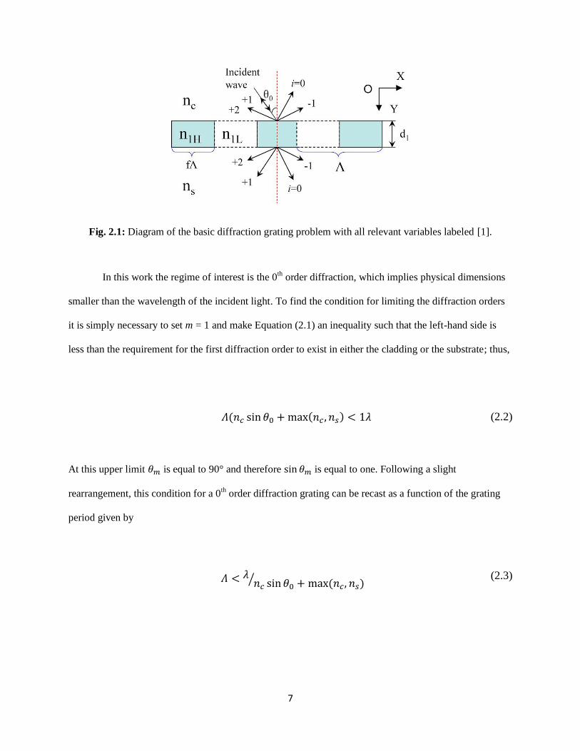
section the naming convention for the variables used in [1] will be followed and is shown in Figure 2.1.
By this convention the area above the grating is referred to as the cladding and below the grating is the
substrate. In Figure 2.1, is the index of the cladding, is the index of the substrate, is the index
of the high index bar, is the index of the low index bar, dl is the grating thickness, is the period of
the grating, and is the angle of incidence. Whether a given diffraction order will be supported is
determined by the grating equation,
(2.1)
where m = 0, ±1, ±2, …, is the diffraction order number, is the angle of the mth order, is the free-
space wavelength of the incident light, and is the index of either the cladding or the substrate
(depending on whether the reflection or transmission order is under investigation, respectively) [1].
7
Fig. 2.1: Diagram of the basic diffraction grating problem with all relevant variables labeled [1].
In this work the regime of interest is the 0th
order diffraction, which implies physical dimensions
smaller than the wavelength of the incident light. To find the condition for limiting the diffraction orders
it is simply necessary to set m = 1 and make Equation (2.1) an inequality such that the left-hand side is
less than the requirement for the first diffraction order to exist in either the cladding or the substrate; thus,
(2.2)
At this upper limit is equal to 90° and therefore is equal to one. Following a slight
rearrangement, this condition for a 0th order diffraction grating can be recast as a function of the grating
period given by
⁄ (2.3)
8
Now that the condition for limiting the number of orders is clear, it is possible to explain the causes and
conditions for extremely high and low reflectivity in these structures.
To understand the reflection characteristics of interest requires a different perspective when
viewing the grating structure. Since the period of the grating is smaller than the wavelength of the
incident light, it is possible to also consider the grating as a waveguide in the x-direction (per Figure 2.1)
with an effective refractive index defined as
(2.4)
with f being the filling factor, which is defined as the ratio of the width of the high index grating bar to the
period of the grating [1], [2]. As a waveguide (assuming that neff > nc, ns), the grating naturally possesses
modes which can propagate in the x direction. However, as these modes propagate down the grating
waveguide, there is some interaction with the alternating refractive index which causes the modes to lose
their energy into either the cladding or substrate. Such modes, known as leaky modes, are characteristic of
the binary grating structures under discussion in this work [2]. In addition to the existence of leaky modes
in the transverse direction of these structures, there is also the ability to excite these modes with a surface
normal incident wave. As mentioned previously, when a surface normal wave is incident on a diffraction
grating, there exist evanescent diffraction orders in the direction parallel to the grating period. When there
is a precise overlap of an evanescent higher order mode and the leaky mode of the grating, energy can be
transferred to the grating waveguide mode. This behavior is known as guided mode resonance (GMR) [2].
The phase matching condition between the incident wave and the transverse waveguide mode can be
written (when the wave is at normal incidence and with the assumption that nc > ns) as

9
(2.5)
It is possible to see this condition for a supported leaky mode graphically by plotting the propagation
constant in the effective waveguide as well as the light lines for the first few evanescent diffraction
orders. An example using the structure parameters nc = 1, d = 0.5 μm, Λ = 1 μm, nh = 2.05, ns = 1.5, f =
0.4, and nf = neff is shown in Figure 2.2.
Fig. 2.2: First Brillouin zone plot of the leaky mode condition in a guided mode resonance. (a) The blue
line represents the real propagation constant of the grating waveguide while the dashed red lines are the
light lines of the evanescent diffraction orders. (b) Shows the imaginary part of the propagation constant
showing the high-loss resonances. (c) Shows the different propagation directions and modes in each
regime [2].
In Figure 2.2(b) we see the various grating stopbands arising from the resonance of an evanescent
higher order mode and the leaky modes of the waveguide (also seen as the intersection of the red and blue
lines in Figure 2.2(a)). In order to achieve the reflectivity characteristics that are the focus of this work, it

10
is necessary to operate at the second stopband, where there are two counter-propagating waveguide
modes which establish a standing wave in the grating layer [3]. It is also important to note that a single
evanescent diffraction order can excite more than one leaky mode in the waveguide grating. The
convention for labeling the coupled modes is, in the TE case, TEm,n where m corresponds to the
diffraction order number and n is the leaky mode number [1], [2]. In Figure 2.3, an example of the
dispersion of the grating is shown as well as the reflectance over the wavelength. As can be seen, at the
exact value of the stopband for the first and second order leaky modes there is a strong peak in reflectance
which corresponds to the peaks in the imaginary part of the propagation constant in Figure 2.2(b).
Fig. 2.3: Diagram of the normalized propagation constant versus normalized wave vector for the first and
second leaky modes of the waveguide grating. Inset shows reflectance versus normalized wave vector
with peaks overlapping the first two stopband values described previously. Note that the normalization
value K = 2π/Λ [3].
At this point it has now been established that in the 0th
order regime of a diffraction grating it is
possible to excite the leaky modes of the grating waveguide layer with a precise overlap of evanescent
modes through the use of GMRs. If the grating structure has been tailored correctly, it is operating in the
second stopband and therefore the leaky modes will transfer their energy into either the zero order
reflected or transmitted wave [3]. With further tailoring of the waveguide characteristics, particularly the
grating thickness (although all grating parameters contribute), it is possible to cause destructive
11
interference at the far end of the grating structure, preventing any of the light in the leaky modes from
coupling into the transmitted wave. As a result, all of the energy instead goes into the reflected order,
resulting in high reflection. All these effects together account for the extremely high reflection
capabilities of the subwavelength grating [4].
Moving forward, the next task is to explain how to obtain the broadband reflection characteristics
that will be expected from these subwavelength gratings. Initially it was thought that gratings could only
have narrow transmission and reflectance peaks; however, it has since been found that in the case of very
high spatial frequency gratings it was possible to get a much broader spectral reaction [5]. This behavior
essentially arises from the fact that the stronger the overlap between the evanescent orders and the leaky
modes, the broader the bandwidth of the spectral reaction [1]. In addition, if the peaks of these high
reflectivity regions exist close enough together, the overlap creates a very broadband high reflectivity
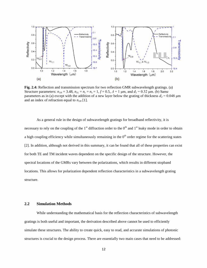
region. To demonstrate, Figure 2.4(a) shows a first attempt at a broadband mirror with the transmissivity
plotted on a logarithmic scale. This highlights the low-transmissivity stopbands each resulting from a
strongly coupled diffraction order – leaky mode pair. In Figure 2.4(b) the structure has been altered so
that two of these stopbands have merged creating a much broader and flatter reflection band with Δλ/λ >
17% with R > 99%, which is precisely the kind of broadband mirror desired for a variety of applications
in lasers.
In the case of Figure 2.4(b), the mixing of the TE1,1 and TE1,0 modes was achieved by adding a
thin high-index layer immediately below the grating structure. In this way essentially the only parameters
that are affected are the effective index and the thickness of the grating waveguide layer, both of which
see a slight increase. In [1] it is also noted that it is not necessary to cause these GMRs to mix as they did
in this example; so long as there is sufficient overlap between two peaks, then a similar broadband, high
reflectivity result can be achieved.
12
Fig. 2.4: Reflection and transmission spectrum for two reflection GMR subwavelength gratings. (a)
Structure parameters: n1H = 3.48, n1L = nc = ns = 1, f = 0.5, Λ = 1 μm, and d1 = 0.32 μm. (b) Same
parameters as in (a) except with the addition of a new layer below the grating of thickness d2 = 0.048 μm
and an index of refraction equal to n1H [1].
As a general rule in the design of subwavelength gratings for broadband reflectivity, it is
necessary to rely on the coupling of the 1st diffraction order to the 0
th and 1
st leaky mode in order to obtain
a high coupling efficiency while simultaneously remaining in the 0th
order regime for the scattering states
[2]. In addition, although not derived in this summary, it can be found that all of these properties can exist
for both TE and TM incident waves dependent on the specific design of the structure. However, the
spectral locations of the GMRs vary between the polarizations, which results in different stopband
locations. This allows for polarization dependent reflection characteristics in a subwavelength grating
structure.
2.2 Simulation Methods
While understanding the mathematical basis for the reflection characteristics of subwavelength
gratings is both useful and important, the derivation described above cannot be used to efficiently
simulate these structures. The ability to create quick, easy to read, and accurate simulations of photonic
structures is crucial to the design process. There are essentially two main cases that need to be addressed:
13
the first is how to immediately see the impact that any given grating parameter has on the spectral
reflection profile and the second is how to see specifically how a grating device structure will behave
under specific conditions. The first simulation technique that will be reviewed considers how to meet the
former criterion.
Rigorous coupled-wave analysis (RCWA), specifically its applications to gratings, was first
developed into its modern form in 1981 by Moharam and Gaylord. Until that point, rigorous and exact
calculations using similar concepts was possible, but computationally intensive [6]. Since that time
numerous variations for more specialized cases, generally aiming to achieve higher computation
efficiencies, have been developed [7 -9]. Without going into much detail, RCWA works by
approximating any arbitrary structure that is periodic in one dimension into several rectangular, binary
layers and solving for all the subsequent boundary conditions. Of course, in the case of the binary,
rectangular profile grating, the exact structure can be used in calculations. The grating structure is
represented by a Fourier series expansion of the complex permittivity for each layer used to approximate
the grating. By casting the phase matching problems into a matrix formalism it is possible to solve
quickly for the diffraction efficiency (essentially the percentage of energy transferred) into each of the
diffraction orders [8]. Of course, in the 0th
order regime the coefficients of the existing diffraction orders
are simply the reflection and transmission coefficients R and T [10]. In the course of solving this problem,
the number of modes in the grating layers is represented by a summation and frequently variations on the
standard RCWA method discuss how quickly increasing the number of modes causes the final result to
converge towards the exact solution.
RCWA is immensely important in subwavelength grating design because of its ease of
implementation in programs such as MATLAB where any two parameters can be swept over and generate
a surface plot showing the resulting reflection coefficient. In the applications that this thesis will focus on,
broad spectral reflectivity is typically one of the most important qualities of these structures and as such
one of the examined parameters is typically the wavelength range of interest. This allows for easy
identification of the parameter values which result in the desired broadband characteristics. Some
14
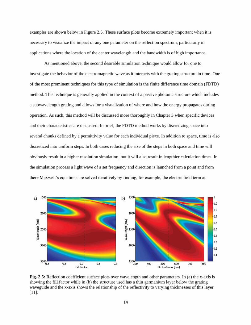
examples are shown below in Figure 2.5. These surface plots become extremely important when it is
necessary to visualize the impact of any one parameter on the reflection spectrum, particularly in
applications where the location of the center wavelength and the bandwidth is of high importance.
As mentioned above, the second desirable simulation technique would allow for one to
investigate the behavior of the electromagnetic wave as it interacts with the grating structure in time. One
of the most prominent techniques for this type of simulation is the finite difference time domain (FDTD)
method. This technique is generally applied in the context of a passive photonic structure which includes
a subwavelength grating and allows for a visualization of where and how the energy propagates during
operation. As such, this method will be discussed more thoroughly in Chapter 3 when specific devices
and their characteristics are discussed. In brief, the FDTD method works by discretizing space into
several chunks defined by a permittivity value for each individual piece. In addition to space, time is also
discretized into uniform steps. In both cases reducing the size of the steps in both space and time will
obviously result in a higher resolution simulation, but it will also result in lengthier calculation times. In
the simulation process a light wave of a set frequency and direction is launched from a point and from
there Maxwell’s equations are solved iteratively by finding, for example, the electric field term at
Fig. 2.5: Reflection coefficient surface plots over wavelength and other parameters. In (a) the x-axis is
showing the fill factor while in (b) the structure used has a thin germanium layer below the grating
waveguide and the x-axis shows the relationship of the reflectivity to varying thicknesses of this layer
[11].
15
time t0 and then using this to solve for the magnetic field at time t0 + 0.5Δt. At this point the magnetic
field is used to solve for the electric field at time t0 + Δt. Following this process it is possible to simply
propagate the electromagnetic wave through these steps in time while simultaneously matching all of the
boundary conditions given by any arbitrary structure. This modeling technique is important both to be
able to verify a given grating’s ability to reflect at the desired wavelengths and also to ensure energy flow
is acceptable in any complex device structure. It is also very important in the context of structures which
do not utilize a complete grating while still relying on broadband reflectivity, an example of which will be
shown in Chapter 3.
2.3 Grating Design Methodology
Having developed a theoretical understanding of the underlying causes of the reflection
characteristics of subwavelength gratings, as well as the methods used to simulate these structures, the
next important challenge to address is how to design the gratings. Given the ability of RCWA to
efficiently calculate the reflectivity coefficient for a span of parameter values, it is to be expected that this
tool will play a central role in most design algorithms. In most cases the material choice is predetermined
and so the only parameters to investigate are the ones determining the physical shape of the grating
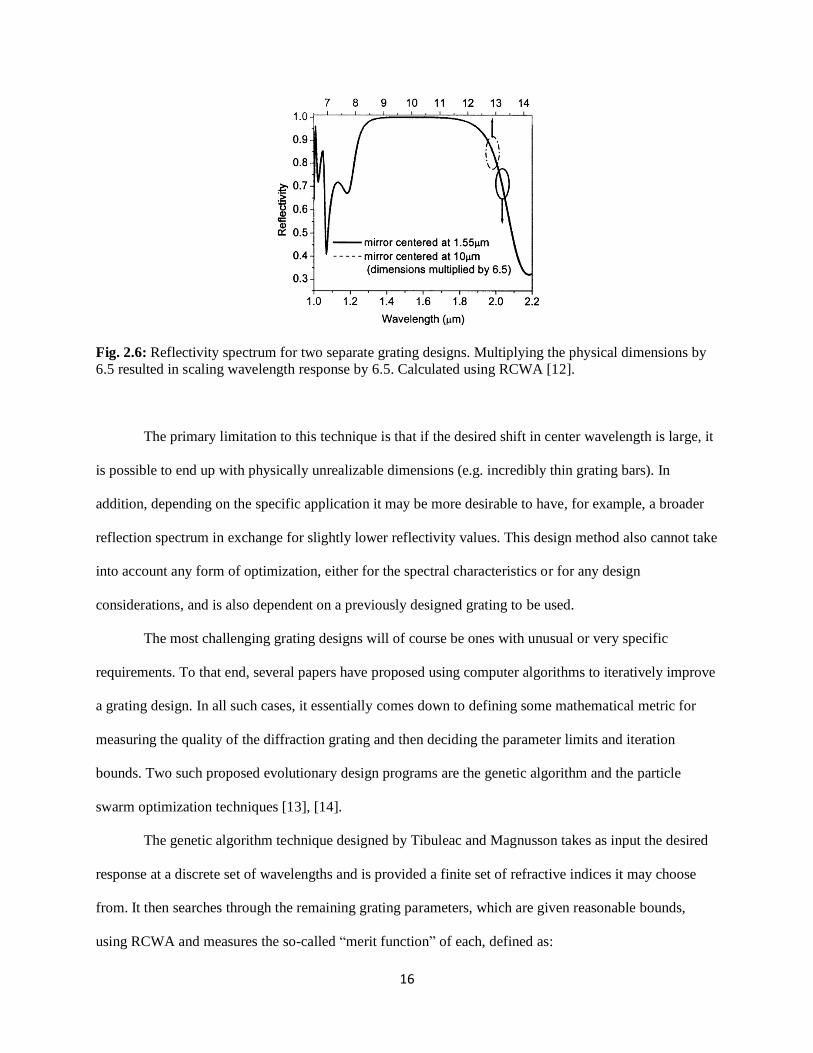
structure. Perhaps among the simplest methods proposed is to scale the physical parameters of the
subwavelength grating by a constant factor. Since the spectral range and position are dependent on the
physical dimensions of the grating, the result is that the spectral reflectivity is scaled by the same factor
[12]. The ability to do so is highlighted in Figure 2.6 where the calculated reflectivity profile is identical
except for spectral location which was altered by scaling the physical dimensions by a factor of 6.5.
16
Fig. 2.6: Reflectivity spectrum for two separate grating designs. Multiplying the physical dimensions by
6.5 resulted in scaling wavelength response by 6.5. Calculated using RCWA [12].
The primary limitation to this technique is that if the desired shift in center wavelength is large, it
is possible to end up with physically unrealizable dimensions (e.g. incredibly thin grating bars). In
addition, depending on the specific application it may be more desirable to have, for example, a broader
reflection spectrum in exchange for slightly lower reflectivity values. This design method also cannot take
into account any form of optimization, either for the spectral characteristics or for any design
considerations, and is also dependent on a previously designed grating to be used.
The most challenging grating designs will of course be ones with unusual or very specific
requirements. To that end, several papers have proposed using computer algorithms to iteratively improve
a grating design. In all such cases, it essentially comes down to defining some mathematical metric for
measuring the quality of the diffraction grating and then deciding the parameter limits and iteration
bounds. Two such proposed evolutionary design programs are the genetic algorithm and the particle
swarm optimization techniques [13], [14].
The genetic algorithm technique designed by Tibuleac and Magnusson takes as input the desired
response at a discrete set of wavelengths and is provided a finite set of refractive indices it may choose
from. It then searches through the remaining grating parameters, which are given reasonable bounds,
using RCWA and measures the so-called “merit function” of each, defined as:
17
[
∑
]
(2.6)
where DEGA,i is the diffraction efficiency in the genetic algorithm grating at wavelength index i and DEref,i
is the diffraction efficiency from the reference data points. M is the total number of reference data points
that were initially provided to the algorithm. Essentially the algorithm measures all the possible designs
within the initial parameter range and returns the minimum merit function as the most suitable design
[13].
Another, more recently developed, iterative computer algorithm that has been proposed is particle
swarm optimization. Similarly to the genetic algorithm, it defines its own value for measuring design
quality, in this case called the fitness factor (FF) which is defined as
[
∑[ ]
]
(2.7)
Again, M is the number of data points from the reference set. Unlike the genetic algorithm, particle swarm
optimization begins by first generating a set of “particles,” which are grating designs with random
parameters that fall within the specified limits. Each particle is also given a random “velocity,” which is
essentially the rate of change of the different physical parameters. After each iteration stage, the FF for
each particle is measured and its velocity is altered by the change in its FF as well as the success of other
particles’ FF changes. As one particle begins to approach optimization, the rest of the particles rapidly
take on its velocity values and so the entire set “swarms” to the optimal design [14].
In both of these iterative design algorithms, one of the most attractive characteristics is the ability
to define the merit or fitness factor to include any constraints that are important for a given application.
While simply scaling or using RCWA surface plots to make small adjustments to an existing design are
18
very useful methods for basic applications of subwavelength gratings, these iterative computer programs
are very important for the more specialized structures needed as well as for finding new designs to utilize.
2.4 References
[1] T. Sang, L. Wang, S. Ji, Y. Ji, H. Chen, and Z. Wang, “Systematic study of the mirror effect in a
Poly-Si subwavelength periodic membrane,” Journal of the Optical Society of America A, vol. 26,
pp. 559-565, 2009.
[2] Y. Ding and R. Magnusson, “Band gaps and leaky-wave effects in resonant photonic-crystal
waveguides,” Optics Express, vol. 15, pp. 680-694, 2007.
[3] R. Magnusson and M. Shokooh-Saremi, “Physical basis for wideband resonant reflectors,” Optics
Express, vol. 16, pp. 3456-3462, 2008.
[4] D. Rosenblatt, A. Sharon, and A. A. Friesem, “Resonant grating waveguide structures,” IEEE
Journal of Quantum Electronics, vol. 33, pp. 2038-2059, 1997.
[5] D. L. Brundrett, E. N. Glytsis, and T. K. Gaylord, “Normal-incidence guided-mode resonant
grating filters: Design and experimental demonstration,” Optics Letters, vol. 23, pp. 700-702,
1998.
[6] M. G. Moharam and T. K. Gaylord, “Rigorous coupled-wave analysis of planar-grating
diffraction,” Journal of the Optical Society of America, vol. 71, pp. 811-818, 1981.
[7] M. G. Moharam, D. A. Pommet, E. B. Grann, and T. K. Gaylord, “Stable implementation of the
rigorous coupled-wave analysis for surface-relief gratings: Enhanced transmittance matrix
approach,” Journal of the Optical Society of America, vol. 12, pp. 1077-1086, 1995.
[8] M. G. Moharam, E. B. Grann, D. A. Pommet, and T. K. Gaylord, “Formulation for stable and
efficient implementation of the rigorous coupled-wave analysis of binary gratings,”Journal for
the Optical Society of America, vol. 12, pp. 1068-1076, 1995.
[9] P. Lalanne and G. M. Morris, “Highly improved convergence of the coupled-wave method for
TM polarization,” Journal for the Optical Society of America, vol. 13, pp. 779-784, 1996.
[10] J.-S. Ye, Y. Kanamori, F.-R. Hu, and K. Hane, “Self-supported subwavelength gratings with a
broad band of high reflectance analysed by the rigorous coupled-wave method,” Journal of
Modern Optics, vol. 53, pp. 1995-2004, 2006.
[11] J. M. Kontio, J. Simonen, K. Leinonen, M. Kuittinen, and T. Niemi, “Broadband infrared mirror
using guided-mode resonance in a subwavelength germanium grating,” Optics Letters, vol. 35,
pp. 2564-2566, 2010.

19
[12] C. F. R. Mateus, M. C. Y. Huang, Y. Deng, A. R. Neureuther, and C. J. Chang-Hasnain,
“Ultrabroadband mirror using low-index cladded subwavelength grating,” IEEE Photonics
Technology Letters, vol. 16, pp. 518-520, 2004.
[13] S. Tibuleac and R. Magnusson, “Narrow-linewidth bandpass filters with diffractive thin-film
layers,” Optics Letters, vol. 26, pp. 584-586, 2001.
[14] M. Shokooh-Saremi and R. Magnusson, “Particle swarm optimization and its application to the
design of diffraction grating filters,” Optics Letters, vol. 32, pp. 894-896, 2007.
20
Chapter 3
Applications with VCSELs
3.1 Vertical-Cavity Surface-Emitting Lasers
The focus of this thesis is the theory and applications of subwavelength gratings, particularly
when applied to vertical-cavity surface-emitting lasers. Chapter 2 has discussed how subwavelength
gratings function, how they are modeled, and how they are designed. Before considering applications of
the gratings, it is important to review the basics of VCSELs in terms of their structure, operation, and how
they are characterized.
As mentioned in Chapter 1, the first VCSELs were proposed by Iga in the late 1970s and since
the late 1980s demonstration of continuous wave operation, they have been an area of intense research
[1], [2]. The VCSEL structure possesses several innate advantages over edge emitting lasers such as a
circular beam output, the ability to test the device without cleaving, and the potential for two-dimensional
arrays [3]. The most basic laser design is a gain medium surrounded by mirrors. With sufficient
reflectance and some method of creating a population inversion within the gain medium, spontaneous
emission is overtaken by stimulated emission and so the resulting output is coherent light. The basic idea
of a VCSEL is to epitaxially define the gain medium with surrounding mirrors parallel to the wafer
surface. This type of structure results in a much smaller gain volume than would be found in an edge
emitting laser design and therefore necessitates much higher reflectivity mirrors in order to increase the
cavity photon lifetime and thereby achieve lasing. The most effective and common solution today is to
epitaxially define distributed Bragg reflector (DBR) mirrors on each side of the gain region. As discussed
briefly in Chapter 1, monolithic DBRs consist of alternating pairs of semiconductor layers with different
refractive indices, each a quarter of a wavelength thick. The resulting multiple reflections from each
21
dielectric interface leads to constructive interference effects which result in high reflectivity. Of course
there are many different considerations that go into VCSEL design which are outside the scope of this
work, but some of the more general areas of interest include lateral current and photon confinement, the
transparency of the materials of the DBR to the wavelength of interest, and carrier recombination outside
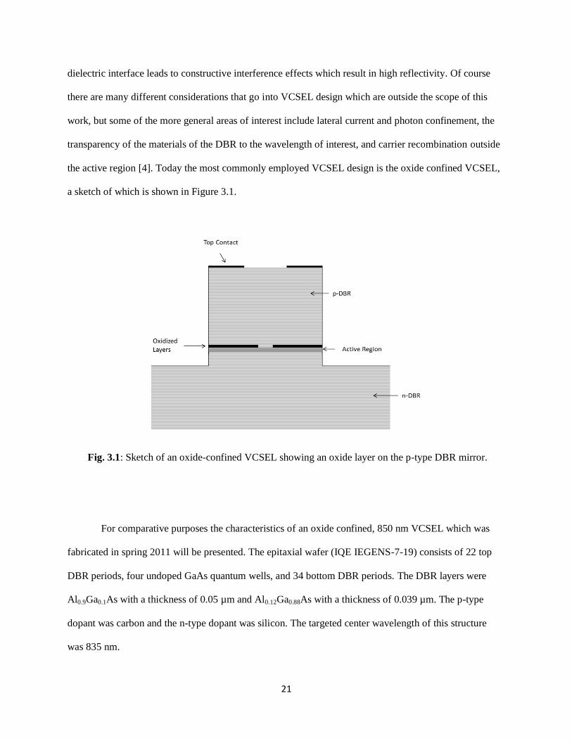
the active region [4]. Today the most commonly employed VCSEL design is the oxide confined VCSEL,
a sketch of which is shown in Figure 3.1.
Fig. 3.1: Sketch of an oxide-confined VCSEL showing an oxide layer on the p-type DBR mirror.
For comparative purposes the characteristics of an oxide confined, 850 nm VCSEL which was
fabricated in spring 2011 will be presented. The epitaxial wafer (IQE IEGENS-7-19) consists of 22 top
DBR periods, four undoped GaAs quantum wells, and 34 bottom DBR periods. The DBR layers were
Al0.9Ga0.1As with a thickness of 0.05 µm and Al0.12Ga0.88As with a thickness of 0.039 µm. The p-type
dopant was carbon and the n-type dopant was silicon. The targeted center wavelength of this structure
was 835 nm.

22
This wafer was fabricated using a bottom metal contact deposition (AuGe/Ni/Au), a patterned top
metal contact (Ti/Au), and a mesa etch. Lateral oxidation was performed to provide the current
confinement. Several different mesa diameters were fabricated on the sample and tested. In general (with
some variation across the wafer) it was found the 30 µm mesa possessed a 5 x 5 µm2 oxide aperture. An
image of the wafer following fabrication is shown in Figure 3.2.
Fig. 3.2: Top view of fabricated oxide-confined VCSELs.
For characterization purposes, the most important data for any laser design is the LIV plot, which
shows the light output (L) and applied voltage (V) as functions of injection current (I). To obtain this, the
sample was placed on a probe station with probes connected to a current source. A microscope with an
optical fiber was used to direct the light output of the VCSELs to an optical spectrum analyzer (OSA). To
perform LIV measurements, the current was controlled by a semiconductor parameter analyzer (SPA)
with all the collected data being organized by a workstation running LabVIEW 6.1 which could then be
saved to a Microsoft Excel spreadsheet. A typical LIV dataset collected from a 5 x 5 µm aperture device
is shown in Figure 3.3. Some important values that can be derived from these plots include the threshold
current and the peak output power of the VCSEL.
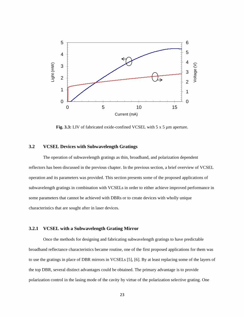
23
Fig. 3.3: LIV of fabricated oxide-confined VCSEL with 5 x 5 µm aperture.
3.2 VCSEL Devices with Subwavelength Gratings
The operation of subwavelength gratings as thin, broadband, and polarization dependent
reflectors has been discussed in the previous chapter. In the previous section, a brief overview of VCSEL
operation and its parameters was provided. This section presents some of the proposed applications of
subwavelength gratings in combination with VCSELs in order to either achieve improved performance in
some parameters that cannot be achieved with DBRs or to create devices with wholly unique
characteristics that are sought after in laser devices.
3.2.1 VCSEL with a Subwavelength Grating Mirror
Once the methods for designing and fabricating subwavelength gratings to have predictable
broadband reflectance characteristics became routine, one of the first proposed applications for them was
to use the gratings in place of DBR mirrors in VCSELs [5], [6]. By at least replacing some of the layers of
the top DBR, several distinct advantages could be obtained. The primary advantage is to provide
polarization control in the lasing mode of the cavity by virtue of the polarization selective grating. One
0
1
2
3
4
5
6
0
1
2
3
4
5
0 5 10 15
Vo
lta
ge
(V
)
Lig
ht (m
W)
Current (mA)
24
characteristic of a VCSEL is that it naturally possesses a single longitudinal mode due to the short cavity
length; however, the lasing mode tends to operate in between two polarizations due to a variety of effects
[7]. Using a subwavelength grating in one of the VCSEL mirrors, however, provides polarization
dependent reflectivity, and having even slightly higher reflectance for one polarization over the other
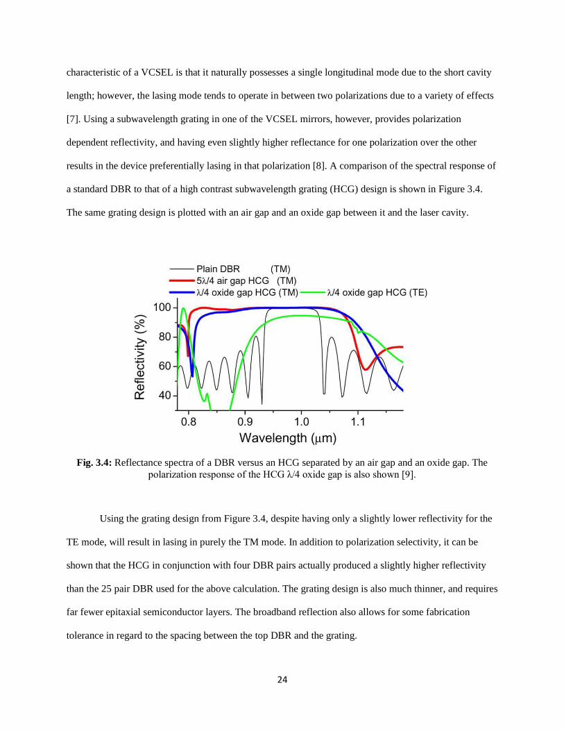
results in the device preferentially lasing in that polarization [8]. A comparison of the spectral response of
a standard DBR to that of a high contrast subwavelength grating (HCG) design is shown in Figure 3.4.
The same grating design is plotted with an air gap and an oxide gap between it and the laser cavity.
Fig. 3.4: Reflectance spectra of a DBR versus an HCG separated by an air gap and an oxide gap. The
polarization response of the HCG λ/4 oxide gap is also shown [9].
Using the grating design from Figure 3.4, despite having only a slightly lower reflectivity for the
TE mode, will result in lasing in purely the TM mode. In addition to polarization selectivity, it can be
shown that the HCG in conjunction with four DBR pairs actually produced a slightly higher reflectivity
than the 25 pair DBR used for the above calculation. The grating design is also much thinner, and requires
far fewer epitaxial semiconductor layers. The broadband reflection also allows for some fabrication
tolerance in regard to the spacing between the top DBR and the grating.
25
Another advantage to using subwavelength gratings in place of a DBR is reduced parasitic
heating. One of the primary considerations in DBR design is that as current passes through the multiple
layers, the energy band differences from layer to layer in the conduction and valence band for electrons
and holes, respectively, lead to a considerable amount of non-radiative, thermal recombination [3]. The
resulting heating can in fact lead to higher spectral mismatch between the cavity and gain spectral
alignment, reducing overall device efficiency. In order to overcome this challenge, a variety of complex
methods may be employed which generally result in lower tolerances for the doping profiles and layer
thicknesses. Using a subwavelength grating reduces the number of layers the current needs to pass
through, and since the entire upper mirror is thinner it actually reduces the complexity of creating a lateral
current injection device as well. For example, a DBR consisting of 35-40 periods on the order of 5 µm
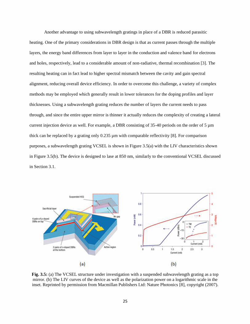
thick can be replaced by a grating only 0.235 µm with comparable reflectivity [8]. For comparison
purposes, a subwavelength grating VCSEL is shown in Figure 3.5(a) with the LIV characteristics shown
in Figure 3.5(b). The device is designed to lase at 850 nm, similarly to the conventional VCSEL discussed
in Section 3.1.
Fig. 3.5: (a) The VCSEL structure under investigation with a suspended subwavelength grating as a top
mirror. (b) The LIV curves of the device as well as the polarization power on a logarithmic scale in the
inset. Reprinted by permission from Macmillan Publishers Ltd: Nature Photonics [8], copyright (2007).

26
Despite the various advantages of using subwavelength gratings in place of DBRs, the fabrication
issues which currently exist prevent them from large scale industrial integration. However, in one specific
regime, subwavelength gratings show significant promise for VCSEL design. Of obvious interest in the
field of communication are the wavelengths of 1.3 and 1.55 µm. However, the material systems which
can lase at these wavelengths (InGaAsP/InP) do not have lattice matched alloys which can create a
reasonable (<40 period) DBR to reflect these wavelengths [10]. As a result, in order to produce a DBR
VCSEL, it becomes necessary to grow the DBR separately from a different material system and then
wafer-bond it to the active region [3]. Such techniques, while technically viable, are expensive and time-
consuming. Since the subwavelength grating generally uses air as one of its alternating layers, it is
possible to obtain the necessary index contrast that results in a high reflectivity mirror while
simultaneously providing the aforementioned polarization selectivity to the device, another feature that
would aid optical communication applications. Such a device was designed and fabricated for operation at
both 1.32 and 1.55 µm ([11] and [10], respectively) utilizing a subwavelength grating as the top mirror. In
the case of the 1.55 µm device, a 45 pair DBR was still used for the bottom mirror, which is undesirable
for mass production. However, the 1.32 µm design included a hybrid mirror for the bottom, which, in
conjunction with the top grating mirror, resulted in an incredibly compact VCSEL design that still
operated in a long wavelength regime, although the bottom dielectric mirror requires complex fabrication
techniques.
It should be noted that DBRs do have the ability to reduce the number of layers required for high
reflectivity if they utilize materials with higher index contrast. However, finding such high contrast
indices in addition to optical transparency at the lasing wavelength, not to mention lattice-matched
materials that can be grown easily on the active region, significantly reduces the number of possible
materials, and using them generally necessitates using lateral current injection [3]. Since subwavelength
27
gratings are fabricated as surface relief gratings, they are able to use an air gap as one of the alternate
refractive indices, allowing the creation of thin, high reflectivity mirrors.
3.2.2 Tunable VCSEL
While the advantages of using a subwavelength grating in place of a DBR have been presented,
currently these advantages are not significant enough to justify switching to gratings in the standard
VCSEL design due to their fabrication complexity which will be detailed further in Section 3.3. However,
in specific applications such as the long-wavelength VCSEL discussed above, gratings present an
immediate advantage and this is one of the main reasons they are under study. Another device in which
gratings can provide significant advantages is the tunable wavelength VCSEL. As already mentioned,
VCSELs are highly sought after in a variety of applications due to their high power efficiency and
advantageous output characteristics. In a number of applications, most notably the communication
technique of wavelength division multiplexing, it becomes necessary to operate the laser at a number of
different wavelengths. Rather than fabricate numerous different wavelength lasers, which can be
expensive as well as reduce system reliability, it is instead desirable to have a single laser which can
adjust to different center wavelengths [12].
One of the standard ways to achieve a tunable VCSEL is to utilize a mirror structure that can
move in order to physically alter the cavity length. The lasing wavelength is determined by the overlap of
the material gain spectrum and the cavity resonances, which, in the case of VCSELs is typically only one
longitudinal mode. By adjusting the length of the cavity it is possible to cause the laser to shift its
emission wavelength slightly. However, creating a movable structure that can adjust a DBR stack of 25 to
40 periods, which can be anywhere from 3 to 10 µm thick, can be a difficult task, resulting in the need for
high voltage bias and considerable engineering efforts to make the device reliable. However, the varied
characteristics of subwavelength gratings immediately show their utility for this type of application.
Being broadband reflectors, they are well suited for a tunable laser, and being inherently one-dimensional
they are very thin and light and therefore easy to move swiftly and accurately in comparison to the DBR

28
mirror [13]. These devices are fabricated for lateral current injection into the active region while the
grating is suspended in a cantilever structure above the VCSEL. A third contact is attached to the
cantilever and the bias between it and the current injection contact results in an electric field which can
pull the grating mirror closer to the active region. A sketch as well as an SEM of such a device is shown
in Figure 3.6.
Fig. 3.6: (a) Tunable VCSEL design showing the cantilever contact and suspended grating as well as
current injection contact. (b) SEM of the device from above [14].
The device shown in Figure 3.6 was reported to have a tunable wavelength range of 18 nm
centered at approximately 855 nm with a single mode, single polarization output and a tuning speed of
approximately 151 ns. A second device in the same report with slightly different physical dimensions
achieved a tuning speed of 63 ns. By comparison, the tuning speed achieved using a similar technique
with a DBR mirror is about 10 µs.
In a separate report, another group was able to fabricate a device which achieved a tuning range
of 100 nm over the longer wavelength regime centered at approximately 1.3 µm [15]. The ability to work
in the longer wavelength regime is, as described previously, one of the other major advantages of using a
subwavelength grating in place of the DBR, and for obvious reasons having a tunable laser source in this
regime is highly desirable for optical fiber wavelength division multiplexing applications. In addition to
the broad tuning range, the device is also reported to have a higher tuning efficiency, which is a metric for
29
the amount of power needed to adjust the center wavelength, another important characteristic for
industrial applications.
3.2.3 Multiwavelength VCSEL Arrays
While the tunable VCSEL is an elegant and effective solution to the need for multiple VCSEL
output wavelengths, in some situations it might be considered too complicated a fabrication process, too
expensive, or perhaps too fragile a structure. In such a case, a desirable alternative would be to have a
multiwavelength array of VCSELs instead. Previously, multiwavelength VCSEL arrays have been
fabricated utilizing thickness variations either in the DBR mirrors or in the active region to achieve
different lasing wavelengths. However, such techniques are difficult to accomplish with predictable
results [16]. Instead, using subwavelength gratings as the top mirror, it becomes possible to define
multiple wavelength lasers from a two-dimensional array purely lithographically, thereby achieving
cheap, easily manufacturable, and reproducible multiwavelength arrays.
Previously it was mentioned that the lasing wavelength was defined by the overlap of the material
gain spectrum and the resonant cavity wavelength. In the case of the latter, it is actually more accurate to
say the 2π phase condition, which is written as
(3.1)
where Lcavity is the physical length of the laser cavity, m is an integer representing the mode number, λlasing
is the lasing wavelength, and ϕcavity and ϕDBR are the reflected phase shift of the grating mirror and the
DBR mirror, respectively. The trick is to design a series of subwavelength gratings whose thickness and
cladding layers are identical, but by varying only the grating period and fill factor, which can be defined
lithographically as opposed to epitaxially, the phase shift is altered sufficiently to achieve different lasing

30
wavelengths while simultaneously possessing high reflectivity at those wavelengths. While this poses a
challenging design problem, given the appropriate set of tools it is in fact possible to design such
structures for a broad range of wavelength, and the reported theoretical structure showed a wavelength
range of nearly 200 nm [16].
3.2.4 Lateral Coupling VCSEL
A final application utilizing subwavelength gratings in VCSEL devices is the potential for in-
plane lateral coupling output, in a device called a vertical-cavity in-plane-emitting laser. Optical
integration into chip-scale electronics is an area of extreme interest at present, but one of the most
difficult challenges is the ability to efficiently couple light from an on-chip laser to a waveguide. This
problem is noticeable in the case of a VCSEL design, which typically emits light perpendicular to the
wafer surface. However, VCSELs are highly desirable for chip-to-chip communications due to their high
power efficiency. Through the clever use of the subwavelength gratings, it becomes possible to have the
laser emit laterally from the bottom mirror.
As discussed in Chapter 2, the subwavelength grating relies on the existence of the so called
guided mode resonances (GMRs) which are essentially the lateral modes of the grating waveguide and the
evanescent diffraction orders which are perpendicular to the incident light. As long as the grating is large
enough relative to the incident light, all of the optical power that enters the GMRs rapidly leaks into a
diffraction order. However, if the grating is abbreviated in one area and replaced with a simple
waveguide, a small percentage of the energy in the GMRs can couple to the waveguide and thus exit the
VCSEL in the transverse direction [17]. A proposed structure using InAlGaAs quantum wells designed to
emit at 1.31 µm is shown in Figure 3.7. The top DBR consists of five pairs of Si and SiN, which produces
sufficiently high reflectivity, while the bottom mirror consists solely of a SiO2 spacing layer and a Si
grating (as well as waveguide).
31
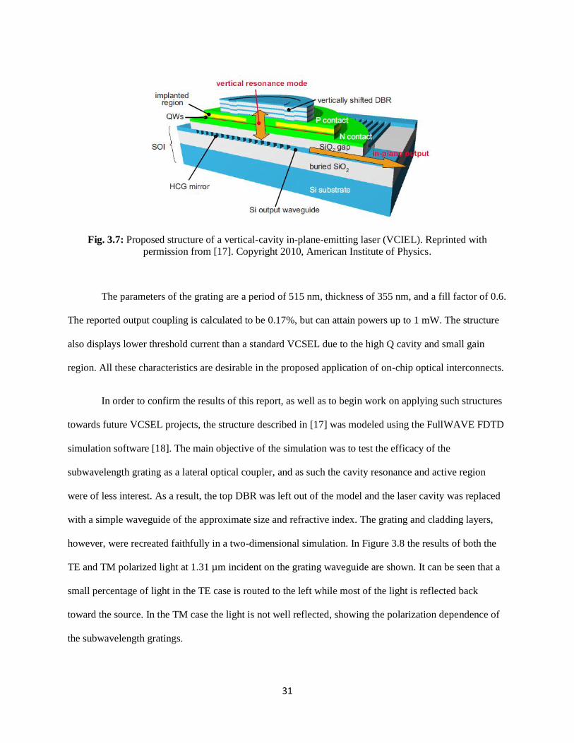
Fig. 3.7: Proposed structure of a vertical-cavity in-plane-emitting laser (VCIEL). Reprinted with
permission from [17]. Copyright 2010, American Institute of Physics.
The parameters of the grating are a period of 515 nm, thickness of 355 nm, and a fill factor of 0.6.
The reported output coupling is calculated to be 0.17%, but can attain powers up to 1 mW. The structure
also displays lower threshold current than a standard VCSEL due to the high Q cavity and small gain
region. All these characteristics are desirable in the proposed application of on-chip optical interconnects.
In order to confirm the results of this report, as well as to begin work on applying such structures
towards future VCSEL projects, the structure described in [17] was modeled using the FullWAVE FDTD
simulation software [18]. The main objective of the simulation was to test the efficacy of the
subwavelength grating as a lateral optical coupler, and as such the cavity resonance and active region
were of less interest. As a result, the top DBR was left out of the model and the laser cavity was replaced
with a simple waveguide of the approximate size and refractive index. The grating and cladding layers,
however, were recreated faithfully in a two-dimensional simulation. In Figure 3.8 the results of both the
TE and TM polarized light at 1.31 µm incident on the grating waveguide are shown. It can be seen that a
small percentage of light in the TE case is routed to the left while most of the light is reflected back
toward the source. In the TM case the light is not well reflected, showing the polarization dependence of
the subwavelength gratings.
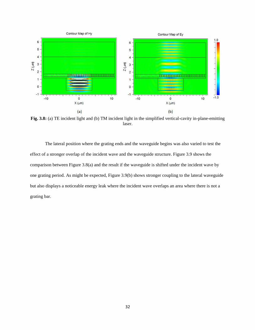
32
Fig. 3.8: (a) TE incident light and (b) TM incident light in the simplified vertical-cavity in-plane-emitting
laser.
The lateral position where the grating ends and the waveguide begins was also varied to test the
effect of a stronger overlap of the incident wave and the waveguide structure. Figure 3.9 shows the
comparison between Figure 3.8(a) and the result if the waveguide is shifted under the incident wave by
one grating period. As might be expected, Figure 3.9(b) shows stronger coupling to the lateral waveguide
but also displays a noticeable energy leak where the incident wave overlaps an area where there is not a
grating bar.

33
Fig. 3.9: (a) Vertical-cavity in-plane-emission structure under 1.31 μm TE incident light. (b) Result with
a shifted waveguide position.
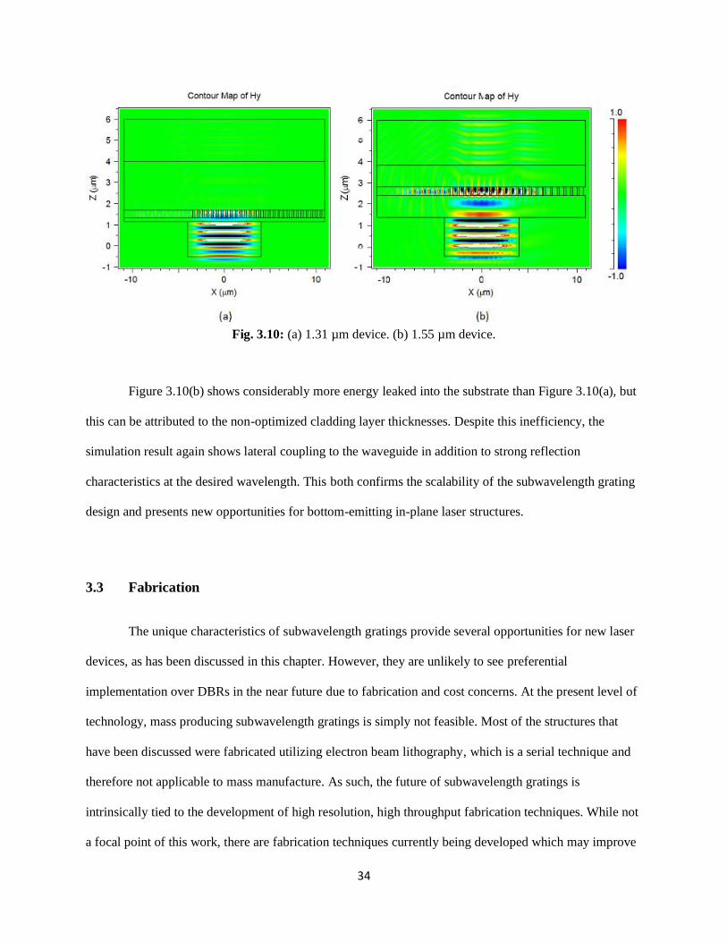
Finally, to test the scalability of the subwavelength grating design, the physical parameters of the
structure were adjusted for a center wavelength of 1.55 µm. This was done by simply multiplying the
grating period and thickness by the ratio of 1.55/1.31 and increasing the cladding layer thicknesses
arbitrarily to enable the effective waveguide. Since the cladding layers were not adjusted for optimization,
the result is predictably less effective than the 1.31 µm design but is still sufficient to show that the
structure can indeed be adjusted to varying center wavelengths. The result is shown next to Figure 3.8(a)
again for comparison.
34
Fig. 3.10: (a) 1.31 µm device. (b) 1.55 µm device.
Figure 3.10(b) shows considerably more energy leaked into the substrate than Figure 3.10(a), but
this can be attributed to the non-optimized cladding layer thicknesses. Despite this inefficiency, the
simulation result again shows lateral coupling to the waveguide in addition to strong reflection
characteristics at the desired wavelength. This both confirms the scalability of the subwavelength grating
design and presents new opportunities for bottom-emitting in-plane laser structures.
3.3 Fabrication
The unique characteristics of subwavelength gratings provide several opportunities for new laser
devices, as has been discussed in this chapter. However, they are unlikely to see preferential
implementation over DBRs in the near future due to fabrication and cost concerns. At the present level of
technology, mass producing subwavelength gratings is simply not feasible. Most of the structures that
have been discussed were fabricated utilizing electron beam lithography, which is a serial technique and
therefore not applicable to mass manufacture. As such, the future of subwavelength gratings is
intrinsically tied to the development of high resolution, high throughput fabrication techniques. While not
a focal point of this work, there are fabrication techniques currently being developed which may improve
35
the odds of manufacturing grating structures. For example, there is nano-imprint fabrication, which
utilizes a mold to form photoresist or a similar compound which can then be used for etching [19]. There
are also numerous works on improving the resolution of standard optical lithography by using, for
example, interference effects [20]. In fact, there is even work on using subwavelength gratings themselves
to create these interference effects in order to achieve higher resolution lithography [21].
3.4 References
[1] H. Soda, K. Iga, C. Kitahara, and Y. Suematsu, “GaInAsP/InP surface emitting injection lasers,”
Japanese Journal of Applied Physics, vol. 18, pp. 2329-2330, 1979.
[2] K. Iga, “Surface-emitting laser- Its birth and generation of new optoelectronics field,” IEEE
Journal on Selected Topics in Quantum Electronics, vol. 6, pp. 1201-1215, 2000.
[3] K. D. Choquette and K. M. Geib, “Fabrication and performance of vertical-cavity surface-
emitting lasers,” in Vertical-Cavity Surface-Emitting Lasers, C. Wilmsen, H. Temkin, and L.
Coldren, Eds. New York: Cambridge Univ. Press, 1999, pp. 193-232.
[4] W. W. Chow, K. D. Choquette, M. H. Crawford, K. L. Lear, and G. R. Hadley, “Design,
fabrication, and performance of infrared and visible vertical-cavity surface-emitting lasers,”
IEEE Journal of Quantum Electronics, Vol. 33, pp. 1810-1824, 1997.
[5] C. F. R. Mateus, M. C. Y. Huang, Y. Deng, A. R. Neureuther, and C. J. Chang-Hasnain,
“Ultrabroadband mirror using low-index cladded subwavelength grating,” IEEE Photonics
Technology Letters, vol. 16, pp. 518-520, 2004.
[6] C. F. R. Mateus, M. C. Y. Huang, L. Chen, and C. J. Chang-Hasnain, “Broad-band mirros (1.12-
1.62 µm) using a subwavelength grating,” IEEE Photonics Technology Letters, vol. 16, pp. 1676-
1678, 2004.
[7] A. Haglund, J. S. Gustavsson, J. bengtsson, P. Jedrasik, and A. Larsson, “Design and evaluation
of fundamental-mode and polarization-stabilized VCSELs with a subwavelength surface grating,”
IEEE Journal of Quantum Electronics, vol. 42, pp. 231-240, 2006.
[8] M. C. Y. Huang, Y. Zhou, and C. J. Chang-Hasnain, “A surface-emitting laser incorporating a
high-index-contrast subwavelength grating,” Nature Photonics, vol. 1, pp. 119-122, 2007.
[9] I-S. Chung, J. Mørk, P. Gilet, and A. Chelnokov, “Subwavelength grating-mirror VCSEL with a
thin oxide gap,” IEEE Photonics Technology Letters, vol. 20, pp. 105-107, 2008.
[10] C. Chase, Y. Rao, W. Hofmann, and C. J. Chang-Hasnain, “1550 nm high contrast grating
VCSEL,” Optics Express, vol. 18, pp. 15461-15466, 2010.
36
[11] W. Hofmann, C. Chase, M. Müller, Y. Rao, C. Grasse, G. Böhm, M.-C. Amann, and C. J. Chang-
Hasnain, “Long-wavelength high-contrast grating vertical-cavity surface-emitting laser,” IEEE
Photonics Journal, vol. 2, pp. 415-422, 2010.
[12] C. J. Chang-Hasnain, “Tunable VCSEL,” IEEE Journal of Selected Topics in Quantum
Electronics, vol. 6, pp. 978-987, 2000.
[13] M. C. Y. Huang, Y. Zhou, and C. J. Chang-Hasnain, “Nano electro-mechanical optoelectronic
tunable VCSEL,” Optics Express, vol. 15, pp. 1222-1227, 2007.
[14] C. J. Chang-Hasnain, Y. Zhou, M. C. Y. Huang, and C. Chase, “High-contrast grating VCSELs,”
IEEE Journal of Selected Topics in Quantum Electronics, vol. 15, pp. 869-878, 2009.
[15] I.-S. Chung, V. Iakovlev, A Sirbu, A. Mereuta, A. Caliman, E. Kapon, and J. Mørk, “Broadband
MEMS-tunable high-index-contrast subwavelength grating long-wavelength VCSEL,” IEEE
Journal of Quantum Electronics, vol. 46, pp. 1245-1253, 2010.
[16] V. Karagodsky, B. Pesala, C. Chase, W. Hofmann, F. Koyama, and C. J. Chang-Hasnain,
“Monolithically integrated multi-wavelength VCSEL arrays using high-contrast gratings,” Optics
Express, vol. 18, pp. 694-699, 2010.
[17] I.-S. Chung and J. Mørk, “Silicon-photonics light source realized by III-V/Si-grating-mirror
laser,” Applied Physics Letters, vol. 97, p. 151113, 2010.
[18] FullWAVE 6.0 Software, RSoft Design Group, 2007.
[19] S.-W. Ahn, K.-D. Lee, J.-S. Kim, S. H. Kim, S. H. Lee, J.-D. Park, and P.-W. Yoon, “Fabrication
of subwavelength aluminum wire grating using nanoimprint lithography and reactive ion
etching,” Microelectronic Engineering, vol. 78-79, pp. 314-318, 2005.
[20] H. Li, X. Zhang, Z. Zhang, X. Luo, and X. Chen, “Fabrication of subwavelength metallic
structures using laser interference lithography,” in 2011 Symposium on Photonics and
Optoelectronics, 2011, p. 4.
[21] E. A. Bezus, L. L. Doskolovich, and N. L. Kazanskiy, “Evanescent-wave interferometric
nanoscale photolithography using guided-mode resonant gratings,” Quantum Electronics, vol. 41,
pp. 759-764, 2011.
37
Chapter 4
Conclusion
4.1 Summary
In this work, the unique properties and potential applications of subwavelength gratings have
been explored, with a particular emphasis on vertical-cavity surface-emitting lasers. These subwavelength
gratings have been shown to be able to possess a polarization dependent response as well as
characteristics such as high reflectivity or transmissivity for narrow and broad spectral ranges. Their small
physical geometry not only makes them promising as mirrors for reduced-size lasers, but also presents
opportunities for other possible applications.
In Chapter 2 the physical basis for the reflection characteristics was defined. A mathematical
representation for these effects, including the existence of the guided mode resonances, was also
presented. In addition to explaining the nature of this phenomenon, the methods employed to model these
structures, rigorous coupled-wave analysis and the finite difference time-domain method, were also
briefly introduced. Finally, some techniques that have been developed to use computer algorithms to aid
in the design of gratings with specific reflection profiles were also explained.
Chapter 3 began with a discussion of the conventional VCSEL architecture and its design
considerations. In addition to explaining the typical parameters of the VCSEL, a sample 850 nm oxide
confined VCSEL was fabricated and presented as an example. After introducing the VCSEL, the different
possible applications using subwavelength gratings with VCSELs was then explored. Several possible
devices were presented including a standard VCSEL structure with a replaced DBR, a tunable VCSEL,
lithographically defined multi-wavelength VCSEL array, and the lateral coupling VCSEL. Using gratings
in these structures presented many inherent advantages over other possible mirrors, especially the DBR.
38
Finally, the fabrication difficulties of producing subwavelength gratings were presented as the primary
factor preventing the adoption of the gratings in any kind of industrial production. A few of the
techniques currently being researched which may help in this regard were also briefly introduced.
4.2 Future Work
Subwavelength gratings have been shown to possess unique characteristics in regard to their
physical dimensions as well as their reflection capabilities. New devices which take advantage of these
properties will continue to be developed and improved upon. Some of the devices presented in this work
are merely theoretical, and investigation into their actual physical performance will be of interest. In
addition, subwavelength lithography is also being researched and, as it develops into feasible
technologies, it may open the path for subwavelength gratings to see more widespread implementation in
VCSELs and other photonic devices.