Embed Size (px)
Citation preview
IJSRST196249 | Received : 08 March 2019 | Accepted : 20 March 2019 | March-April-2019 [ 6 (2) : 246-266]
© 2019 IJSRST | Volume 6 | Issue 2 | Print ISSN: 2395-6011 | Online ISSN: 2395-602X
Themed Section: Science and Technology
DOI : https://doi.org/10.32628/IJSRST196249
246
Modified SVPWM Algorithm for Three Level VSI With Synchronized and Symmetrical Waveforms
Jalla Sowndarya1, M. Shekar2, N. V. Vinay Kumar3 1M.Tech Scholar, Power Electronics and Drives, St.MARK Educational Institution, Soceity Group of Institutions,
Anantapur, Andhra Pradesh, India 2M.Tech, Assistant Professor, St.MARK Educational Institution Soceity Group of Institutions, Anantapur,
Andhra Pradesh, India 3M.Tech, Assistant Professor. GATES Engineering College, Gooty, Andhra Pradesh, India
ABSTRACT
To generate the required reference vector than triangle comparison based PWM techniques for three-level
inverters the space vector based PWM (SVPWM) strategies contain broader choice of switching sequences.
This space vector based PWM technique involves in various steps. These steps are computationally exhaustive.
The SVPWM has been used in three phase inverter control system. The center-aligned PWM is the most
effective way for the Microprocessor Control Unit implementation of the SVPWM, because it can easily
generate the center aligned PWM of the multilevel inverters for generation of the signal of space vector pulse
width modulation (SVPWM), this concept brings out the method. The inverter leg switching times are
generated by this algorithm and middle vector switching times are centered in a sampled interval. The
proposed algorithm does not require any sector identification. And it reduces the computational time as a result.
The adjacent voltage space vectors are forming the small triangles it is called sectors. Multilevel converters can
meet the increasing demand of power ratings and power quality associated with reduced harmonic distortion
and lower electromagnetic interference. Furthermore to optimize switching waveforms, space vector pulse-
width modulation algorithms offer great flexibility among them. Finally the results are verified through
MATLAB/SIMULINK
Keywords : SVPWM Algorithm, VSI, Symmetrical Waveforms, PWM, SVM, FFT, MCU, EMC, ACIM
I. INTRODUCTION
Design the control system for three phase induction
motor with help of modified Space vector modulation
technique. It helps to reduce the harmonic in
inverter design. The modified SVM technique is
harmonic analysis is done by using the FFT based
harmonic analysis. To generate the required
reference vector than triangle comparison based
PWM techniques for three-level inverters the Space
vector based PWM strategies contain broader choice
of switching sequences. This Space Vector based
PWM technique involves in various steps. These
steps are computationally exhaustive. (SVPWM) has
been used in three phase inverter control system. The
center-aligned PWM is the most effective way for the
MCU implementation of the SVPWM, because it can
easily generate the center aligned PWM. For the
multilevel inverters for generation of the signal of
space vector pulse width modulation (SVPWM), this
concept brings out the method. The inverter leg
switching times are generated by this algorithm and
the middle vector switching times are centered, in a
sampled interval. The proposed algorithm does not
require any sector identification. And it reduces the
computational time as a result. The adjacent voltage
International Journal of Scientific Research in Science and Technology (www.ijsrst.com)
Jalla Sowndarya et al. Int J Sci Res Sci Technol. March-April-2019; 6(2) : 246-266
247
space vectors are forming the small triangles. It is
called sectors. Multilevel converters can meet the
increasing demand of power ratings and power
quality associated with reduced harmonic distortion
and lower electromagnetic interference. To optimize
switching waveforms, space vector pulse-width
modulation algorithms offer great flexibility among
them. And they are well suited for digital
implementation.
The concept of the PWM algorithms which is
presented is extended for multilevel inverters. This
paper presents a simple generalized scalar PWM
algorithm for 2, 3 and 5-level inverters. By using
the concept of imaginary switching times the
proposed algorithm has been developed, which are
proportional to the instantaneous sampled phase
voltages only. Moreover, this proposed algorithm
does not require the calculation of angle and
sector information and hence reduces the
complexity involved in the PWM algorithm.
Inverter
A power inverter, or inverter, is an electronic device
or circuitry that changes direct current (DC) to
alternating current (AC). The input voltage, output
voltage and frequency, and overall power handling
depend on the design of the specific device or
circuitry. The inverter does not produce any power;
the power is provided by the DC source. A power
inverter can be entirely electronic or may be a
combination of mechanical effects (such as a rotary
apparatus) and electronic circuitry. Static inverters do
not use moving parts in the conversion process.
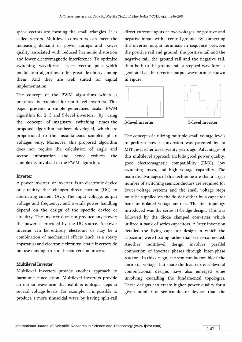
Multilevel Inverter
Multilevel inverters provide another approach to
harmonic cancellation. Multilevel inverters provide
an output waveform that exhibits multiple steps at
several voltage levels. For example, it is possible to
produce a more sinusoidal wave by having split-rail
direct current inputs at two voltages, or positive and
negative inputs with a central ground. By connecting
the inverter output terminals in sequence between
the positive rail and ground, the positive rail and the
negative rail, the ground rail and the negative rail,
then both to the ground rail, a stepped waveform is
generated at the inverter output waveform as shown
in Figure.
3-level inverter 5-level inverter
The concept of utilizing multiple small voltage levels
to perform power conversion was patented by an
MIT researcher over twenty years ago. Advantages of
this multilevel approach include good power quality,
good electromagnetic compatibility (EMC), low
switching losses, and high voltage capability. The
main disadvantages of this technique are that a larger
number of switching semiconductors are required for
lower-voltage systems and the small voltage steps
must be supplied on the dc side either by a capacitor
bank or isolated voltage sources. The first topology
introduced was the series H-bridge design. This was
followed by the diode clamped converter which
utilized a bank of series capacitors. A later invention
detailed the flying capacitor design in which the
capacitors were floating rather than series-connected.
Another multilevel design involves parallel
connection of inverter phases through inter-phase
reactors. In this design, the semiconductors block the
entire dc voltage, but share the load current. Several
combinational designs have also emerged some
involving cascading the fundamental topologies.
These designs can create higher power quality for a
given number of semiconductor devices than the
International Journal of Scientific Research in Science and Technology (www.ijsrst.com)
Jalla Sowndarya et al. Int J Sci Res Sci Technol. March-April-2019; 6(2) : 246-266
248
fundamental topologies alone due to a multiplying
effect of the number of levels.
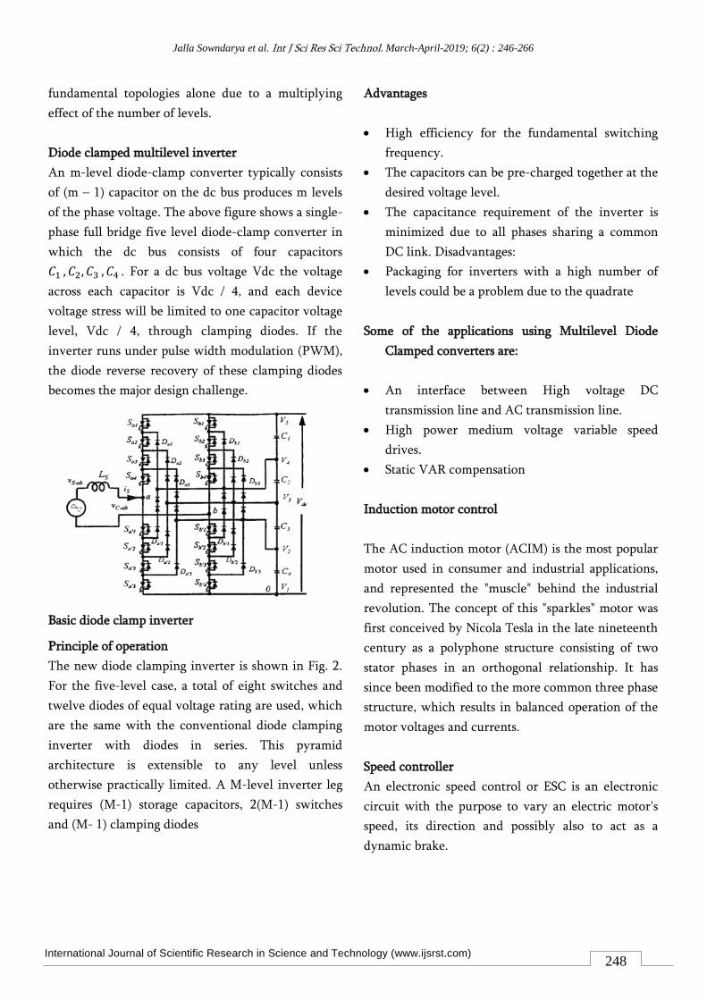
Diode clamped multilevel inverter
An m-level diode-clamp converter typically consists
of (m – 1) capacitor on the dc bus produces m levels
of the phase voltage. The above figure shows a single-
phase full bridge five level diode-clamp converter in
which the dc bus consists of four capacitors
𝐶1 , 𝐶2, 𝐶3 , 𝐶4 . For a dc bus voltage Vdc the voltage
across each capacitor is Vdc / 4, and each device
voltage stress will be limited to one capacitor voltage
level, Vdc / 4, through clamping diodes. If the
inverter runs under pulse width modulation (PWM),
the diode reverse recovery of these clamping diodes
becomes the major design challenge.
Basic diode clamp inverter
Principle of operation
The new diode clamping inverter is shown in Fig. 2.
For the five-level case, a total of eight switches and
twelve diodes of equal voltage rating are used, which
are the same with the conventional diode clamping
inverter with diodes in series. This pyramid
architecture is extensible to any level unless
otherwise practically limited. A M-level inverter leg
requires (M-1) storage capacitors, 2(M-1) switches
and (M- 1) clamping diodes
Advantages
• High efficiency for the fundamental switching
frequency.
• The capacitors can be pre-charged together at the
desired voltage level.
• The capacitance requirement of the inverter is
minimized due to all phases sharing a common
DC link. Disadvantages:
• Packaging for inverters with a high number of
levels could be a problem due to the quadrate
Some of the applications using Multilevel Diode
Clamped converters are:
• An interface between High voltage DC
transmission line and AC transmission line.
• High power medium voltage variable speed
drives.
• Static VAR compensation
Induction motor control
The AC induction motor (ACIM) is the most popular
motor used in consumer and industrial applications,
and represented the "muscle" behind the industrial
revolution. The concept of this "sparkles" motor was
first conceived by Nicola Tesla in the late nineteenth
century as a polyphone structure consisting of two
stator phases in an orthogonal relationship. It has
since been modified to the more common three phase
structure, which results in balanced operation of the
motor voltages and currents.
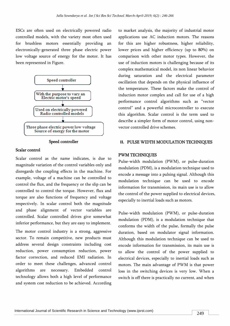
Speed controller
An electronic speed control or ESC is an electronic
circuit with the purpose to vary an electric motor's
speed, its direction and possibly also to act as a
dynamic brake.
International Journal of Scientific Research in Science and Technology (www.ijsrst.com)
Jalla Sowndarya et al. Int J Sci Res Sci Technol. March-April-2019; 6(2) : 246-266
249
ESCs are often used on electrically powered radio
controlled models, with the variety most often used
for brushless motors essentially providing an
electronically-generated three phase electric power
low voltage source of energy for the motor. It has
been represented in Figure.
Speed controller
Scalar control
Scalar control as the name indicates, is due to
magnitude variation of the control variables only and
disregards the coupling effects in the machine. For
example, voltage of a machine can be controlled to
control the flux, and the frequency or the slip can be
controlled to control the torque. However, flux and
torque are also functions of frequency and voltage
respectively. In scalar control both the magnitude
and phase alignment of vector variables are
controlled. Scalar controlled drives give somewhat
inferior performance, but they are easy to implement.
The motor control industry is a strong, aggressive
sector. To remain competitive, new products must
address several design constraints including cost
reduction, power consumption reduction, power
factor correction, and reduced EMI radiation. In
order to meet these challenges, advanced control
algorithms are necessary. Embedded control
technology allows both a high level of performance
and system cost reduction to be achieved. According
to market analysis, the majority of industrial motor
applications use AC induction motors. The reasons
for this are higher robustness, higher reliability,
lower prices and higher efficiency (up to 80%) on
comparison with other motor types. However, the
use of induction motors is challenging because of its
complex mathematical model, its non linear behavior
during saturation and the electrical parameter
oscillation that depends on the physical influence of
the temperature. These factors make the control of
induction motor complex and call for use of a high
performance control algorithms such as “vector
control” and a powerful microcontroller to execute
this algorithm. Scalar control is the term used to
describe a simpler form of motor control, using non-
vector controlled drive schemes.
II. PULSE WIDTH MODULATION TECHNIQUES
PWM TECHNIQUES
Pulse-width modulation (PWM), or pulse-duration
modulation (PDM), is a modulation technique used to
encode a message into a pulsing signal. Although this
modulation technique can be used to encode
information for transmission, its main use is to allow
the control of the power supplied to electrical devices,
especially to inertial loads such as motors.
Pulse-width modulation (PWM), or pulse-duration
modulation (PDM), is a modulation technique that
conforms the width of the pulse, formally the pulse
duration, based on modulator signal information.
Although this modulation technique can be used to
encode information for transmission, its main use is
to allow the control of the power supplied to
electrical devices, especially to inertial loads such as
motors. The main advantage of PWM is that power
loss in the switching devices is very low. When a
switch is off there is practically no current, and when
International Journal of Scientific Research in Science and Technology (www.ijsrst.com)
Jalla Sowndarya et al. Int J Sci Res Sci Technol. March-April-2019; 6(2) : 246-266
250
it is on, there is almost no voltage drop across the
switch.
Zero Voltage Switching Vs. Conventional SVPWM
Multilevel pulse width modulation (PWM) inverters
have been developed to overcome shortcomings in
solid-state switching device ratings, so that large
motors can be controlled by high-power adjustable-
frequency drives. The most popular structure
proposed as a transformer less voltage source inverter
is the diode-clamped converter based on the neutral-
point converter proposed. The two multilevel PWM
methods most discussed in the literature are
multilevel carrier-based PWM and multilevel space-
vector PWM; both are extensions of traditional two
level PWM strategies to several levels. Investigators
have proposed carrier-based multilevel sine-triangle
PWM schemes for control of a multilevel diode-
clamped inverter used as a motor drive or static
variable compensator. Others have generalized space-
vector PWM theory for use with multilevel inverters.
A third PWM method used to control a multilevel
diode-clamped converter is with selective harmonic
elimination. Medium/large motor drives,
uninterruptible power supply (UPS) systems, and
high-power inverters in flexible alternate current
transmission systems (FACTS) need switching
elements which can bear high voltages and currents.
Various PWM approach
To overcome the limitations of semiconductor
switches, several new techniques and topologies have
been developed, such as multiple switching elements
in one leg of an inverter, series-connected inverters,
parallel-connected inverters, multilevel reactive
power compensators, multiple rectifiers for unity
power factor correction, optimization of motor
performance indexes (such as harmonic current,
torque ripple, common mode voltage, and bearing
currents), and neutral-point-clamped (NPC) inverters.
This paper focuses on series-connected voltage-
source PWM inverters. In this area, present control
techniques are based on the following methods:
• Sinusoidal PWM (SPWM),
• Space-vector PWM (SVPWM)
The term multilevel starts with the three-level
inverter introduced by Novae. Nowadays, multilevel
converters are becoming increasingly popular in
power applications, owing to their ability to meet the
increasing demand of power ratings and power
quality associated with reduced harmonic distortion
and lower electromagnetic interference. Multilevel
topologies have been used as rectifiers for the
connection of renewable energy sources to the utility
grid in and as a power-conditioning system of
variable speed wind turbines. The combination of a
large number of semiconductors to achieve high
power ratings is well established. Choosing an
arrangement where all devices are individually
controlled, rather than switched together in series,
provides more control opportunities. Voltage-source
multilevel-inverter topologies, synthesize a voltage
waveform from several voltage levels typically
obtained from several capacitors or dc sources. The
commutation of the power switches permits the
addition of the voltages of these sources, which reach
high voltage at the output, whereas the power
semiconductors must withstand only reduced
voltages.
International Journal of Scientific Research in Science and Technology (www.ijsrst.com)
Jalla Sowndarya et al. Int J Sci Res Sci Technol. March-April-2019; 6(2) : 246-266
251
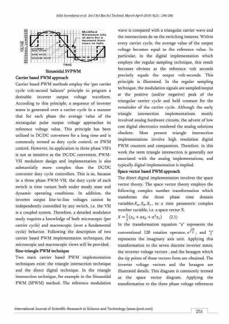
Sinusoidal SVPWM
Carrier based PWM approach
Carrier based PWM methods employ the \per carrier
cycle volt-second balance" principle to program a
desirable inverter output voltage waveform.
According to this principle, a sequence of inverter
states is generated over a carrier cycle in a manner
that for each phase the average value of the
rectangular pulse output voltage approaches its
reference voltage value. This principle has been
utilized in DC/DC converters for a long time and is
commonly termed as duty cycle control, or PWM
control. However, its application to three phase VSI's
is not as intuitive as the DC/DC converters. PWM-
VSI modulator design and implementation is also
substantially more complex than the DC/DC
converter duty cycle controllers. This is so, because
in a three phase PWM-VSI, the duty cycle of each
switch is time variant both under steady state and
dynamic operating conditions. In addition, the
inverter output line-to-line voltages cannot be
independently controlled by any switch, i.e. the VSI
is a coupled system. Therefore, a detailed modulator
study requires a knowledge of both microscopic (per
carrier cycle) and macroscopic (over a fundamental
cycle) behavior. Following the description of two
carrier based PWM implementation techniques, the
microscopic and macroscopic views will be provided.
Sine-triangle PWM technique
Two main carrier based PWM implementation
techniques exist: the triangle intersection technique
and the direct digital technique. In the triangle
intersection technique, for example in the Sinusoidal
PWM (SPWM) method. The reference modulation
wave is compared with a triangular carrier wave and
the intersections de ne the switching instants. Within
every carrier cycle, the average value of the output
voltage becomes equal to the reference value. In
particular, in the digital implementation which
employs the regular sampling technique, this result
becomes obvious as the reference volt seconds
precisely equals the output volt-seconds. This
principle is illustrated. In the regular sampling
technique, the modulation signals are sampled/output
at the positive (and/or negative) peak of the
triangular carrier cycle and held constant for the
remainder of the carrier cycle. Although the early
triangle intersection implementations mostly
involved analog hardware circuits, the advent of low
cost digital electronics rendered the analog solutions
obsolete. Most present triangle intersection
implementations involve high resolution digital
PWM counters and comparators. Therefore, in this
work the term triangle intersection is generally not
associated with the analog implementations, and
typically digital implementation is implied.
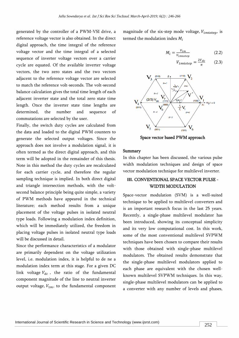
Space vector based PWM approach
The direct digital implementation involves the space
vector theory. The space vector theory employs the
following complex number transformation which
transforms the three phase time domain
variables 𝑋𝑎 , 𝑋𝑏 , 𝑋𝑐 , to a time parametric complex
number variable, i.e. a space vector X.
𝑋 =2
3(𝑥𝑎 + 𝑎𝑥𝑏 + 𝑎2𝑥𝑐) (2.1)
In the transformation equation “a" represents the
conventional 120 rotation operator, 𝑒𝑗2𝜋
3 , and “j”
represents the imaginary axis unit. Applying this
transformation to the seven discrete inverter states,
the inverter voltage vectors , and the hexagon which
the tip points of these vectors form are obtained. The
inverter voltage vectors and the hexagon are
illustrated details. This diagram is commonly termed
as the space vector diagram. Applying the
transformation to the three phase voltage references
International Journal of Scientific Research in Science and Technology (www.ijsrst.com)
Jalla Sowndarya et al. Int J Sci Res Sci Technol. March-April-2019; 6(2) : 246-266
252
generated by the controller of a PWM-VSI drive, a
reference voltage vector is also obtained. In the direct
digital approach, the time integral of the reference
voltage vector and the time integral of a selected
sequence of inverter voltage vectors over a carrier
cycle are equated. Of the available inverter voltage
vectors, the two zero states and the two vectors
adjacent to the reference voltage vector are selected
to match the reference volt-seconds. The volt-second
balance calculation gives the total time length of each
adjacent inverter state and the total zero state time
length. Once the inverter state time lengths are
determined, the number and sequence of
commutations are selected by the user.
Finally, the switch duty cycles are calculated from
the data and loaded to the digital PWM counters to
generate the selected output voltages. Since the
approach does not involve a modulation signal, it is
often termed as the direct digital approach, and this
term will be adopted in the remainder of this thesis.
Note in this method the duty cycles are recalculated
for each carrier cycle, and therefore the regular
sampling technique is implied. In both direct digital
and triangle intersection methods, with the volt-
second balance principle being quite simple, a variety
of PWM methods have appeared in the technical
literature; each method results from a unique
placement of the voltage pulses in isolated neutral
type loads. Following a modulation index definition,
which will be immediately utilized, the freedom in
placing voltage pulses in isolated neutral type loads
will be discussed in detail.
Since the performance characteristics of a modulator
are primarily dependent on the voltage utilization
level, i.e. modulation index, it is helpful to de ne a
modulation index term at this stage. For a given DC
link voltage 𝑉𝑑𝑐 , the ratio of the fundamental
component magnitude of the line to neutral inverter
output voltage, 𝑉1𝑚, to the fundamental component
magnitude of the six-step mode voltage, 𝑉1𝑚6step, is
termed the modulation index 𝑀𝑖
𝑀𝑖 =𝑉1𝑚
𝑉1𝑚6𝑠𝑡𝑒𝑝 (2.2)
𝑉1𝑚6𝑠𝑡𝑒𝑝 =2𝑉𝑑𝑐
𝜋 (2.3)
Space vector based PWM approach
Summary
In this chapter has been discussed, the various pulse
width modulation techniques and design of space
vector modulation technique for multilevel inverter.
III. CONVENTIONAL SPACE VECTOR PULSE -
WIDTH MODULATION
Space-vector modulation (SVM) is a well-suited
technique to be applied to multilevel converters and
is an important research focus in the last 25 years.
Recently, a single-phase multilevel modulator has
been introduced, showing its conceptual simplicity
and its very low computational cost. In this work,
some of the most conventional multilevel SVPWM
techniques have been chosen to compare their results
with those obtained with single-phase multilevel
modulators. The obtained results demonstrate that
the single-phase multilevel modulators applied to
each phase are equivalent with the chosen well-
known multilevel SVPWM techniques. In this way,
single-phase multilevel modulators can be applied to
a converter with any number of levels and phases,
International Journal of Scientific Research in Science and Technology (www.ijsrst.com)
Jalla Sowndarya et al. Int J Sci Res Sci Technol. March-April-2019; 6(2) : 246-266
253
avoiding the use of conceptually and mathematically
complex SVPWM strategies.
Voltage source inverters (VSI) are used to generate
three phase variable voltage and variable frequency
of AC supply. In many applications AC three phase
variable supply is required. Generally AC voltage is
defined by amplitude and frequency. This algorithm
essentially controls these two quantities. SVPWM
controls average output voltage in a sampling period
by producing switching pulses of variable duty cycles.
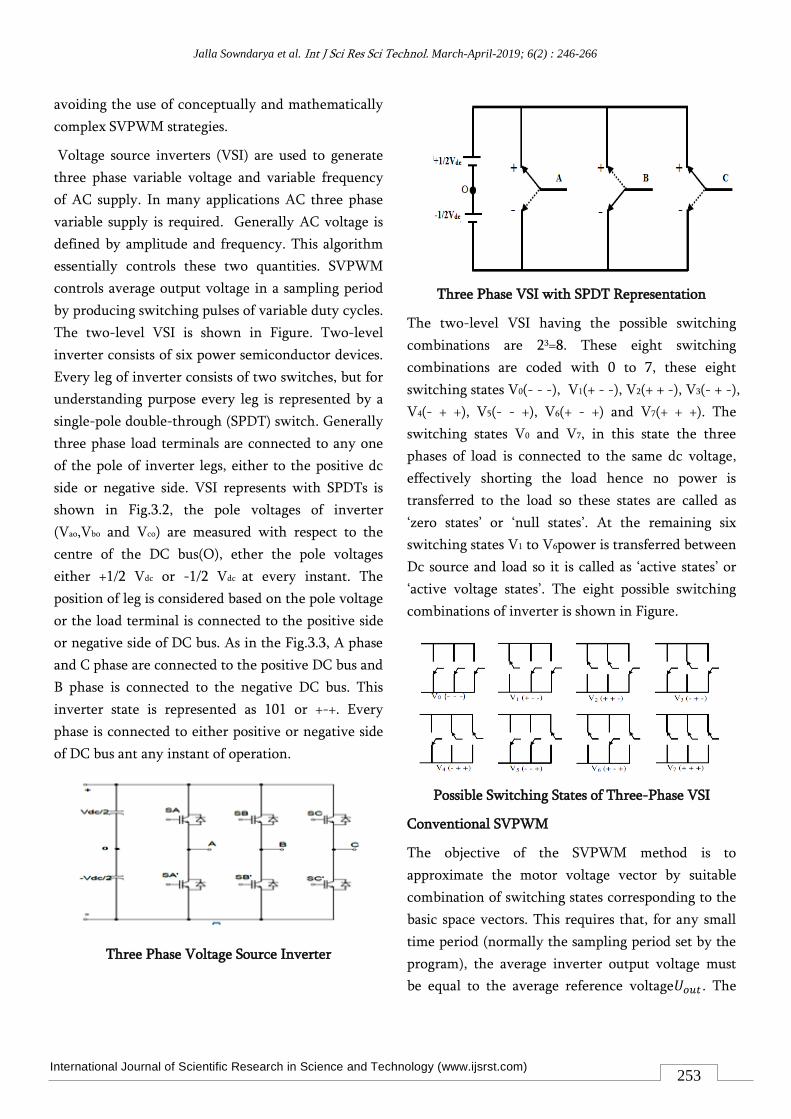
The two-level VSI is shown in Figure. Two-level
inverter consists of six power semiconductor devices.
Every leg of inverter consists of two switches, but for
understanding purpose every leg is represented by a
single-pole double-through (SPDT) switch. Generally
three phase load terminals are connected to any one
of the pole of inverter legs, either to the positive dc
side or negative side. VSI represents with SPDTs is
shown in Fig.3.2, the pole voltages of inverter
(Vao,Vbo and Vco) are measured with respect to the
centre of the DC bus(O), ether the pole voltages
either +1/2 Vdc or -1/2 Vdc at every instant. The
position of leg is considered based on the pole voltage
or the load terminal is connected to the positive side
or negative side of DC bus. As in the Fig.3.3, A phase
and C phase are connected to the positive DC bus and
B phase is connected to the negative DC bus. This
inverter state is represented as 101 or +-+. Every
phase is connected to either positive or negative side
of DC bus ant any instant of operation.
Three Phase Voltage Source Inverter
Three Phase VSI with SPDT Representation
The two-level VSI having the possible switching
combinations are 23=8. These eight switching
combinations are coded with 0 to 7, these eight
switching states V0(- - -), V1(+ - -), V2(+ + -), V3(- + -),
V4(- + +), V5(- - +), V6(+ - +) and V7(+ + +). The
switching states V0 and V7, in this state the three
phases of load is connected to the same dc voltage,
effectively shorting the load hence no power is
transferred to the load so these states are called as
‘zero states’ or ‘null states’. At the remaining six
switching states V1 to V6power is transferred between
Dc source and load so it is called as ‘active states’ or
‘active voltage states’. The eight possible switching
combinations of inverter is shown in Figure.
Possible Switching States of Three-Phase VSI
Conventional SVPWM
The objective of the SVPWM method is to
approximate the motor voltage vector by suitable
combination of switching states corresponding to the
basic space vectors. This requires that, for any small
time period (normally the sampling period set by the
program), the average inverter output voltage must
be equal to the average reference voltage𝑈𝑜𝑢𝑡 . The
International Journal of Scientific Research in Science and Technology (www.ijsrst.com)
Jalla Sowndarya et al. Int J Sci Res Sci Technol. March-April-2019; 6(2) : 246-266
254
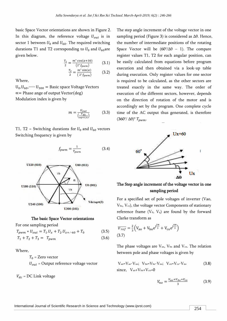
basic Space Vector orientations are shown in Figure 2.
In this diagram, the reference voltage 𝑈𝑜𝑢𝑡 is in
sector 1 between 𝑈0 and 𝑈60. The required switching
durations T1 and T2 corresponding to 𝑈0 and 𝑈60are
given below.
𝑇1
2=
𝑚∗ cos(𝛼+30)
(2∗𝑓𝑝𝑤𝑚) (3.1)
𝑇2
2=
𝑚∗ sin(𝛼)
( 2∗𝑓𝑝𝑤𝑚) (3.2)
Where,
U0,U60,∙∙∙∙∙∙ U300 = Basic space Voltage Vectors
∝= Phase ange of output Vector(deg)
Modulation index is given by
𝑚 =𝑈𝑜𝑢𝑡
(𝑉𝑑𝑐
𝑠𝑞𝑟𝑡(3)) (3.3)
T1, T2 = Switching durations for 𝑈0 and 𝑈60 vectors
Switching frequency is given by
𝑓𝑝𝑤𝑚 =1
𝑇𝑝𝑤𝑚 (3.4)
The basic Space Vector orientations
For one sampling period
𝑇𝑝𝑤𝑚 ∗ 𝑈𝑜𝑢𝑡 = 𝑇1∙𝑈𝑥 + 𝑇2∙𝑈𝑥+⋰∙60 + 𝑇0 (3.5)
𝑇1 + 𝑇2 + 𝑇3 = 𝑇𝑝𝑤𝑚 (3.6)
Where,
𝑇0 = Zero vector
𝑈𝑜𝑢𝑡 = Output reference voltage vector
𝑉𝑑𝑐 = DC Link voltage
The step angle increment of the voltage vector in one
sampling period (Figure 3) is considered as ∆θ. Hence,
the number of intermediate positions of the rotating
Space Vector will be (60°/∆θ – 1). The compare
register values T1, T2 for each angular position, can
be easily calculated from equations before program
execution and then obtained via a look-up table
during execution. Only register values for one sector
is required to be calculated, as the other sectors are
treated exactly in the same way. The order of
execution of the different sectors, however, depends
on the direction of rotation of the motor and is
accordingly set by the program. One complete cycle
time of the AC output thus generated, is therefore
(360°/ ∆θ)* 𝑇𝑝𝑤𝑚.
The Step angle increment of the voltage vector in one
sampling period
For a specified set of pole voltages of inverter (Vao,
Vbo, Vco), the voltage vector Components of stationary
reference frame (Vd, Vq) are found by the forward
Clarke transform as
𝑣 𝑟𝑒𝑓̅̅ ̅̅ ̅̅ =2
3(Vao + Vboej
2π
3 + Vcoej4π
3 )
(3.7)
The phase voltages are Van, Vbn and Vcn. The relation
between pole and phase voltages is given by
Van=Vao-Vno; Vbn=Vbo-Vno; Vcn=Vco-Vno (3.8)
since, Van+Vbn+Vcn=0
𝑉𝑛𝑜 =𝑉𝑎𝑜+𝑉𝑏𝑜+𝑉𝑐𝑜
3 (3.9)
International Journal of Scientific Research in Science and Technology (www.ijsrst.com)
Jalla Sowndarya et al. Int J Sci Res Sci Technol. March-April-2019; 6(2) : 246-266
255
From (3.1) and (3.2) it is clear that the phase voltages
Van,Vbn, Vcn also result in the same space vector Vref̅̅ ̅̅ ̅.
The space vector Vref̅̅ ̅̅ ̅ can also be determined into two
stationary frame namely Vdand Vq. The relationship
between the instantaneous phase voltages Van,Vbn, Vcn
and stationary components Vd, Vq can be given by the
conventional three-phase to two-phase
transformation as follows:
[Vq
Vd] =
2
3[1 −
1
2−
1
2
0√3
2−
√3
2
] [
Van
Vbn
Vcn
] (3.10)
The instantaneous three phase voltages can be
represented by a space vector in stationary reference
frame. The vector having constant magnitude it is
equal to the amplitude of voltages. The vector is
revolving with angular speed ω=2πf. The eight
possible switching states of VSI are indicated as
voltage space vectors in a two-level space plane as
shown in Fig.
The active states can be represented by space vectors
each of magnitude Vdc and divides the space vector
plane into six equal sectors as shown in Fig.2.1. It can
be shown that all the six active states can be
represented by space vectors given by (3.5) forming a
regular hexagon and dividing the space plane into six
sectors each of 600, denoted as 1,2,…,6 as shown in
Fig.
VS = Vdc ∗ ej(S−1)Π/3, S = 1,2, . . ,6. (3.11)
A group of switching states can be used, for
maintaining the volt-second balance to generate
during a sub cycle. This grouping of switching states,
which generate a sample, is called as a ‘switching
sequence’. There are certain limitations, which must
be imposed so as to produce a PWM waveform,
which results in minimum ripple. Group of switching
states are operating in a sample of time means to
achieve desired value of output voltage. But it
required some information regarding vector, where
the tip of reference vector is located (number of
sector), which are the nearer active and null states to
operate a group.
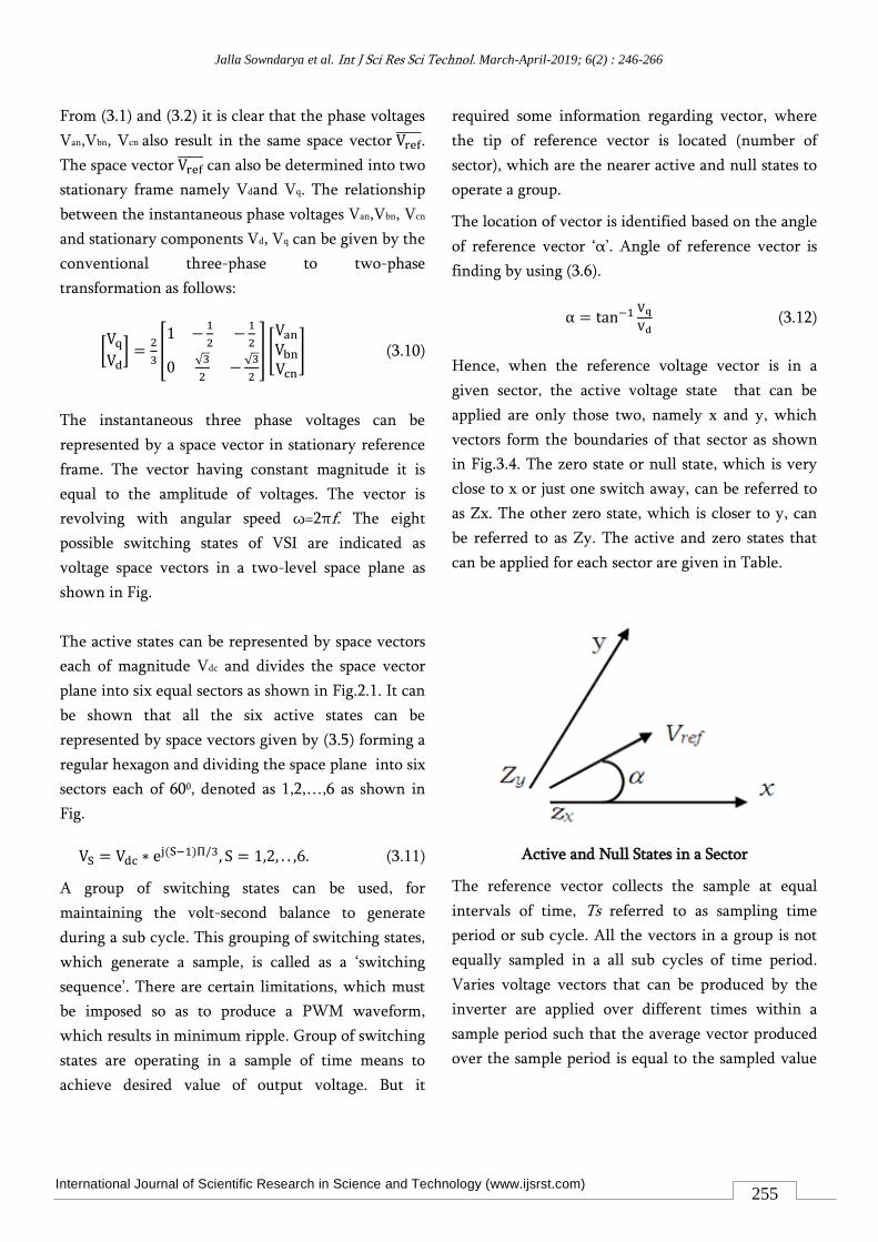
The location of vector is identified based on the angle
of reference vector ‘α’. Angle of reference vector is
finding by using (3.6).
α = tan−1 Vq
Vd (3.12)
Hence, when the reference voltage vector is in a
given sector, the active voltage state that can be
applied are only those two, namely x and y, which
vectors form the boundaries of that sector as shown
in Fig.3.4. The zero state or null state, which is very
close to x or just one switch away, can be referred to
as Zx. The other zero state, which is closer to y, can
be referred to as Zy. The active and zero states that
can be applied for each sector are given in Table.
Active and Null States in a Sector
The reference vector collects the sample at equal
intervals of time, Ts referred to as sampling time
period or sub cycle. All the vectors in a group is not
equally sampled in a all sub cycles of time period.
Varies voltage vectors that can be produced by the
inverter are applied over different times within a
sample period such that the average vector produced
over the sample period is equal to the sampled value
International Journal of Scientific Research in Science and Technology (www.ijsrst.com)
Jalla Sowndarya et al. Int J Sci Res Sci Technol. March-April-2019; 6(2) : 246-266
256
of the reference vector, in terms of angle (frequency)
and magnitude.
Table : Active and Null States for Each Sector
Angle
‘α’ Sector Zx X Y Zy
0-60 1 0 1 2 7
60-120 2 7 2 3 0
120-180 3 0 3 4 7
180-240 4 7 4 5 0
240-300 5 0 5 6 7
300-360 6 7 6 1 0
As all the six sectors are equal, here the discussion is
restricted to sector-I only. Let T1, T2 and TZ be the
duration for which the active states 1, active states 2
and zero state are to be applied respectively in a
given sampling time period From the principle of
volt-sec balance T1, T2and Tz can be calculate
𝑉𝑟𝑒𝑓∠α° = 2
3Vdc∠0° ∗ T1 +
2
3Vdc∠60° ∗ T2 + 0 ∗ Tz
(3.13)
𝑉𝑟𝑒𝑓(cos 𝛼 + 𝑗 sin 𝛼) ∗ 𝑇𝑠 =2
3𝑉𝑑𝑐 ∗ 𝑇1 +
2
3𝑉𝑑𝑐(cos 60° + 𝑗 sin 60°) ∗ 𝑇2 (3.14)
By equating imaginary and real terms
𝑉𝑟𝑒𝑓 cos 𝛼 ∗ 𝑇𝑠 =2
3𝑉𝑑𝑐 ∗ 𝑇1 +
2
3𝑉𝑑𝑐 cos 60° ∗ 𝑇2
(3.15)
𝑉𝑟𝑒𝑓 sin 𝛼 ∗ 𝑇𝑠 =2
3𝑉𝑑𝑐 sin 60° ∗ 𝑇2 (3.16)
From (3.9) and (3.10)
𝑇1 =𝑀𝑖∗𝑇𝑠∗ sin(60°−𝛼)
sin 60° (3.17)
𝑇2 =𝑀𝑖∗𝑇𝑠 ∗ sin 𝛼
sin 60° (3.18)
Here Mi is modulation index 𝑀𝑖 =3
2
𝑉𝑟𝑒𝑓
𝑉𝑑𝑐
Tz=Ts-T1-T2(3.19)
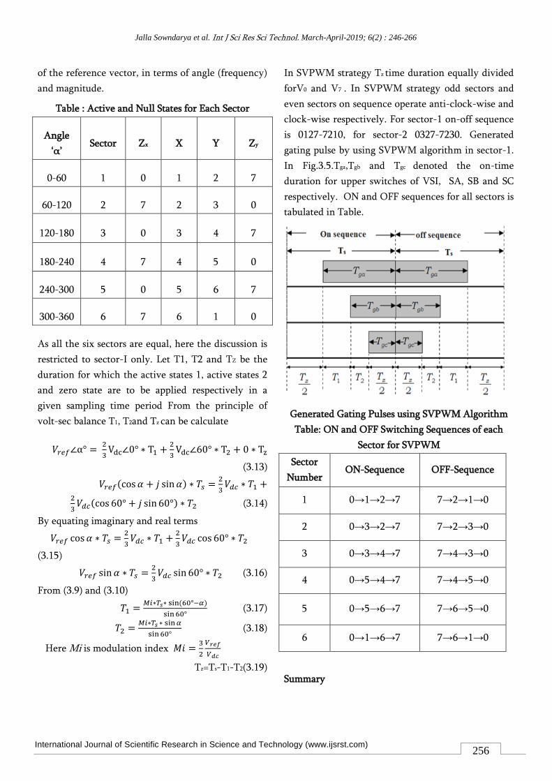
In SVPWM strategy Tz time duration equally divided
forV0 and V7 . In SVPWM strategy odd sectors and
even sectors on sequence operate anti-clock-wise and
clock-wise respectively. For sector-1 on-off sequence
is 0127-7210, for sector-2 0327-7230. Generated
gating pulse by using SVPWM algorithm in sector-1.
In Fig.3.5.Tga,Tgb and Tgc denoted the on-time
duration for upper switches of VSI, SA, SB and SC
respectively. ON and OFF sequences for all sectors is
tabulated in Table.
Generated Gating Pulses using SVPWM Algorithm
Table: ON and OFF Switching Sequences of each
Sector for SVPWM
Sector
Number ON-Sequence OFF-Sequence
1 0→1→2→7 7→2→1→0
2 0→3→2→7 7→2→3→0
3 0→3→4→7 7→4→3→0
4 0→5→4→7 7→4→5→0
5 0→5→6→7 7→6→5→0
6 0→1→6→7 7→6→1→0
Summary
International Journal of Scientific Research in Science and Technology (www.ijsrst.com)
Jalla Sowndarya et al. Int J Sci Res Sci Technol. March-April-2019; 6(2) : 246-266
257
Study about the Pulse with modulation technique for
multilevel inverter, and also know about take the
well know knowledge about the conventional
modulation technique. The modulation technique is
used inverter for maintain the harmonic level in the
output voltage and current. That space vector level is
increase the output comes well and low THD value.
IV. PROPOSED ALGORITHM FOR SVPWM
The Proposed space vector pulse width modulation
(SVPWM) scheme is to reduce THD. In comparison
with the traditional modulation scheme, under the
Proposed strategy, the changing of switch states cause
only one single phase voltage change at a time. Thus,
the switching loss can be reduced. Using this novel
modulation strategy, the changing of switch states
cause only one single phase voltage change every
time. The simulation study of space vector
modulation technique of two levels Inverter reveals
that space vector modulation technique utilizes DC
bus voltage more efficiently and generates less
harmonic distortion. All these methods aim at
generating a sinusoidal inverter output voltage
without lower-order harmonics. This is possible if
the sampling frequency is high compared to the
fundamental output frequency of the inverter. The
performance of each of these control methods is
usually judged based on the Total Harmonic
Distortion (THD) of the voltage at the output of the
inverter. The objective of this section is to propose
and recommend modified SVPWM schemes that are
best suitable for specific applications. Applications
can be distinguished mainly based on their power
level and hence the switching frequency or by
the type of load. The choice of modification in
SVPWM scheme was governed mainly by the
performance criteria, namely THD. Analysis was
first performed for each of these schemes to
develop expressions for each scheme. Then the
scheme was simulated in MATLAB/SIMULINK to
verify the expressions developed.
In the first part of this chapter, the efficiency of
SVPWM is matched and compared with that of
SPWM. Based on the comparison made on the
factors like THD, RMS AC voltage and
harmonics spectrum, it is inferred that SVPWM
technique has low distortion, higher RMS voltage,
superior performance characteristics and extended
output capabilities compared to SPWM technique at
near-rated speed. Hence SVPWM technique is
recommended for near-rated speed operation.
Conversely, at low speed, the harmonic distortion is
less in SPWM technique. Hence SPWM is suggested
for low speed operation. Also it can be proposed that
a hybrid approach of SPWM for lower speed
operations with SVPWM for near-rated speed
operation could yield the best usage of these two
techniques.
Conditions for synchronization, TPS, HWS and QWS
in terms of pole voltages
The processing of synchronization of the clock signal
frequency with triangular carrier frequency is
explained.
Synchronization
The synchronization is process to operate the
inverter output voltage work same with respect to
fundamental voltage. This process done by the PWM
with satisfies the following condition
VRO (2π ± θ) = VRO(θ)
VYO(2π±θ)=VYO(θ) (4.1)
VBO (2π ± θ )= VBO(θ)
The synchronization process must need to low
switching frequency.
TPS (Three phase symmetry)
The three phase symmetry is necessary at low
switching frequency for eliminate the low order
harmonics. In these eliminate process the PWM is
must satisfy the following condition.
VRO(θ)=VYO(θ+(2π/3))=VBO(θ-(2π/3)) (4.2)
or
International Journal of Scientific Research in Science and Technology (www.ijsrst.com)
Jalla Sowndarya et al. Int J Sci Res Sci Technol. March-April-2019; 6(2) : 246-266
258
VRO (θ+(2π/3)) = VBO (θ)
VYO(θ+(2π/3))=VRO(θ) (4.3)
VBO (θ+(2π/3)) = VYO(θ)
HWS (Half wave symmetry)
The half wave symmetry eliminates the harmonics in
the output voltage. That process is achieved by the
pole voltage with opposite condition of it is angel and
it is angel with 90° phase angle.
VRO (π ± θ) = -VRO(θ)
VYO (π ± θ) = - VYO(θ) (4.4)
VBO (π ± θ ) = - VBO(θ)
Table: Conditions for Synchronization, TPS, HWS
Synchro
nization HWS TPS TPS
Pole
voltage
at θ
Pole
voltage
at
θ ± 2π
Pole
voltage
at
θ ± π
Pole
voltage
at
θ+(2π/3
)
Pole
voltage
at θ-
(2π/3)
VRO VRO -VRO VBO VYO
VYO VYO -VYO VRO VBO
VBO VBO -VBO VYO VRO
QWS (Quarter wave symmetry)
A combination of half-wave symmetry with either
even or odd symmetry results in a wave with quarter-
wave symmetry. For example, it Posses half-wave
symmetry as well as odd symmetry. The wave shown
in Fig. possesses both half-wave symmetry and even
symmetry. The analytical test of quarter-wave
symmetry is as follows: Odd quarter-wave.
The conditions for quarter-wave symmetry are as
follows
For even quarter-wave:
f(t)=-f(𝑡 + 𝑇
2)andf(t)=f(-t) (4.5)
For odd quarter-wave
f(t)=-f(𝑡 + 𝑇
2)andf(t)=f(-t) (4.6)
Here, θPR, θPY and θPB are the instants at which the R-
phase, Y-phase and B-phase fundamental waveforms
have their positive or negative peaks respectively.
Table: Conditions for QWS
Pole voltage at θPR+ θ Pole voltage at θPR- θ
VRO VRO
VYO VYO
VBO VBO
The conditions for synchronization and TPS, HWS
and QWS are summarized in Tables
Conditions for synchronization, TPS, HWS and QWS
in terms of inverter states
Synchronization:
The word synchronization is coincide the time or
rate between two signals. The fundamental voltage
and out voltage is synchronization with time rate.
That is achieving by the pulse width modulation by
using the conditions.
Three phase symmetry
A centered or symmetric PWM signal is
characterized by modulated pulses which are
centered with respect to each PWM period. The
advantage of a symmetric PWM signal over an
asymmetric PWM signal is that it has two inactive
zones of the same duration: at the beginning and at
the end of each PWM period. This symmetry has
been shown to cause less harmonics than an
asymmetric PWM signal in the phase currents of an
ac motor, such as induction and dc brushless motors,
when sinusoidal modulation is used. Figure shows
two examples of symmetric PWM waveforms.
The generation of a symmetric PWM waveform with
a compare unit is similar to the generation of an
asymmetric PWM waveform. The only exception is
that GP timer 1 (or GP timer 3) now needs to be put
International Journal of Scientific Research in Science and Technology (www.ijsrst.com)
Jalla Sowndarya et al. Int J Sci Res Sci Technol. March-April-2019; 6(2) : 246-266
259
in continuous up-/down-counting mode. There are
usually two compare matches in a PWM period in
symmetric PWM waveform generation, one during
the upward counting before period match, and
another during downward counting after period
match. A new compare value becomes effective after
the period match (reload on period) because it makes
it possible to advance or delay the second edge of a
PWM pulse. An application of this feature is when a
PWM waveform modification compensates for
current errors caused by the dead-band in ac motor
control. Because the compare registers are shadowed,
a new value can be written to them at any time
during a period. For the same reason, new values can
be written to the action and period registers at any
time during a period to change the PWM period or to
force changes in the PWM output definition.
Symmetric PWM waveforms
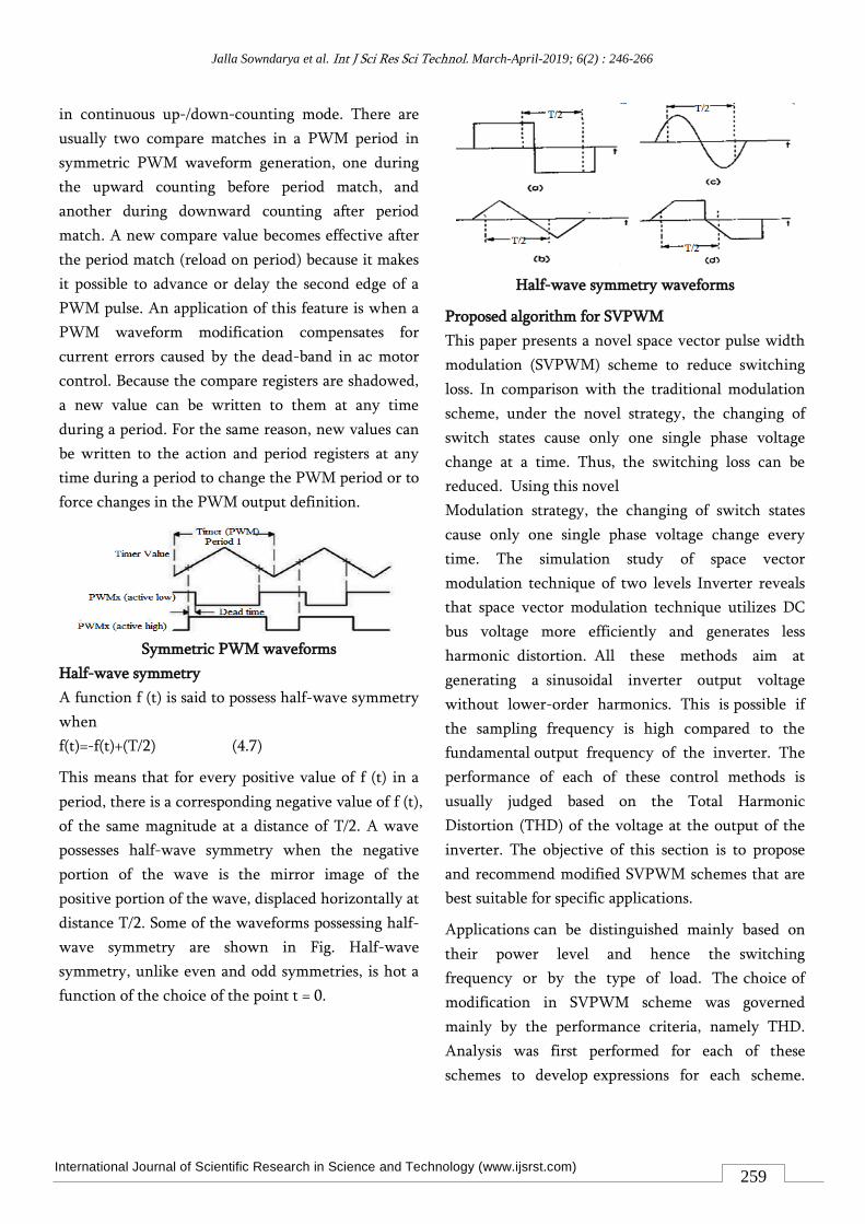
Half-wave symmetry
A function f (t) is said to possess half-wave symmetry
when
f(t)=-f(t)+(T/2) (4.7)
This means that for every positive value of f (t) in a
period, there is a corresponding negative value of f (t),
of the same magnitude at a distance of T/2. A wave
possesses half-wave symmetry when the negative
portion of the wave is the mirror image of the
positive portion of the wave, displaced horizontally at
distance T/2. Some of the waveforms possessing half-
wave symmetry are shown in Fig. Half-wave
symmetry, unlike even and odd symmetries, is hot a
function of the choice of the point t = 0.
Half-wave symmetry waveforms
Proposed algorithm for SVPWM
This paper presents a novel space vector pulse width
modulation (SVPWM) scheme to reduce switching
loss. In comparison with the traditional modulation
scheme, under the novel strategy, the changing of
switch states cause only one single phase voltage
change at a time. Thus, the switching loss can be
reduced. Using this novel
Modulation strategy, the changing of switch states
cause only one single phase voltage change every
time. The simulation study of space vector
modulation technique of two levels Inverter reveals
that space vector modulation technique utilizes DC
bus voltage more efficiently and generates less
harmonic distortion. All these methods aim at
generating a sinusoidal inverter output voltage
without lower-order harmonics. This is possible if
the sampling frequency is high compared to the
fundamental output frequency of the inverter. The
performance of each of these control methods is
usually judged based on the Total Harmonic
Distortion (THD) of the voltage at the output of the
inverter. The objective of this section is to propose
and recommend modified SVPWM schemes that are
best suitable for specific applications.
Applications can be distinguished mainly based on
their power level and hence the switching
frequency or by the type of load. The choice of
modification in SVPWM scheme was governed
mainly by the performance criteria, namely THD.
Analysis was first performed for each of these
schemes to develop expressions for each scheme.
International Journal of Scientific Research in Science and Technology (www.ijsrst.com)
Jalla Sowndarya et al. Int J Sci Res Sci Technol. March-April-2019; 6(2) : 246-266
260
Then the scheme was simulated in
MATLAB/Simulink to verify the expressions
developed.
The steps involved in a simplified algorithm
Sector identification
The sector identification can be done by using
coordinate transformation of the reference vector
into a two dimensional coordinate system. The sector
can also be determined by resolving the reference
phase vector along a, b and c axis and by repeated
comparison with discrete phase voltages. After
identifying the sector, the voltage vectors at the
vertices of the sector are to be determined. Once the
switching voltage space vectors are determined the
switching sequences can be identified. The
calculations of the duration of the voltage vectors can
be simplified by mapping the identified sector
correspond to a sector of two-level inverter. To
obtain optimum switching, the voltage vectors are to
be switched for their respective durations, in a
sequence such that only one switching occurs as the
inverter moves from one switching state to another.
But as the level of the inverter increases, the sector
identification, switching vector determination and
dwelling time calculation becomes more complex.
The computational complexity and execution time
increases. The duty cycles of reference voltage vector
will be m1, m2 and 1 − (m1 + m2). The values of m1
and m2 are useful in identifying the region where
reference vector is located, which is the major
problem in case of multi-level inverters. In this paper,
a correction to the duty cycles of reference vector is
applied to easily identify the location of reference
vector in each region of multi-level inverter. Then
the appropriate switching sequence of the identified
region and calculation of switching times for each
state with the obtained duty cycles are estimated.
This new SVPWM algorithm can be extended to
higher level inverters also.
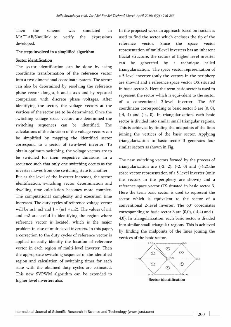
In the proposed work an approach based on fractals is
used to find the sector which encloses the tip of the
reference vector. Since the space vector
representation of multilevel inverters has an inherent
fractal structure, the sectors of higher level inverter
can be generated by a technique called
triangularization. The space vector representation of
a 5-level inverter (only the vectors in the periphery
are shown) and a reference space vector OX situated
in basic sector 3. Here the term basic sector is used to
represent the sector which is equivalent to the sector
of a conventional 2-level inverter. The 60°
coordinates corresponding to basic sector 3 are (0, 0),
(-4, 4) and (-4, 0). In triangularization, each basic
sector is divided into similar small triangular regions.
This is achieved by finding the midpoints of the lines
joining the vertices of the basic sector. Applying
triangularization to basic sector 3 generates four
similar sectors as shown in Fig.
The new switching vectors formed by the process of
triangularization are (-2, 2), (-2, 0) and (-4,2).the
space vector representation of a 5-level inverter (only
the vectors in the periphery are shown) and a
reference space vector OX situated in basic sector 3.
Here the term basic sector is used to represent the
sector which is equivalent to the sector of a
conventional 2-level inverter. The 60° coordinates
corresponding to basic sector 3 are (0,0), (-4,4) and (-
4,0). In triangularization, each basic sector is divided
into similar small triangular regions. This is achieved
by finding the midpoints of the lines joining the
vertices of the basic sector.
Sector identification
International Journal of Scientific Research in Science and Technology (www.ijsrst.com)
Jalla Sowndarya et al. Int J Sci Res Sci Technol. March-April-2019; 6(2) : 246-266
261
Shifting the modulating waves to the first sector
The proposed scheme also works in over modulation
region. If the tip of the reference space vector OX lies
outside the hexagon, it will be considered as over
modulation region of operation. During over
modulation, the vector representing sub hexagon
center is not switched. The two other active vectors
will switch for the entire
Sample period.
Shifting the modulating waves to the first sector
Subsector identification
(a) Subsector identification
Applying triangularization to basic sector 3 generates
four similar sectors .The new switching vectors
formed by the process of triangularization are (-2,2),
(-2,0) and (-4,2). Further triangularization will
generate sixteen small sectors. The centric of each
sector is also calculated as the average value of the
vertices enclosing the sector. The sector with its
centric closest to the tip of the reference space vector
is taken as the sector of operation. The sector of
operation identified for reference space vector OX is
sector with number 14
b). Subsector identification
Computation of dwell times
Computation of dwell times
We can easily determine the dwell vector is ' V1 and '
V2 . The ' V0 can be taken as the zero vector in the 2-
level SVPWM. So, we can get the following function:
𝑉1∙𝑇𝑋 + 𝑉2
∙𝑇𝑌 + 𝑉0∙ 𝑇𝑍 = 𝑉𝑟𝑒𝑓
∙ 𝑇𝑆 (4.8)
𝑇𝑋 + 𝑇𝑌 + 𝑇𝑍 = 𝑇𝑆 (4.9)
Combine the equation
(𝑉1 − 𝑉𝑚𝑎𝑝1)𝑇𝑋 + (𝑉2 − 𝑉𝑚𝑎𝑝1)𝑇𝑌 + (𝑉0 −
𝑉𝑚𝑎𝑝1)𝑇𝑍 = (𝑉𝑟𝑒𝑓 − 𝑉𝑚𝑎𝑝1)𝑇𝑆 (4.10)
So,
𝑇𝑋 + 𝑉2𝑇𝑌 + 𝑉0𝑇𝑍 = 𝑉𝑟𝑒𝑓𝑇𝑆 (4.11)
The dwell time of ' V1 , ' V2 , and ' V0 can be
calculated, the original vector dwell time can be
determined. From the mapping in Figure 5, the
vector selection and the dwell time calculation of the
3-level SVPWM are converted to 2-level SVPWM
totally.
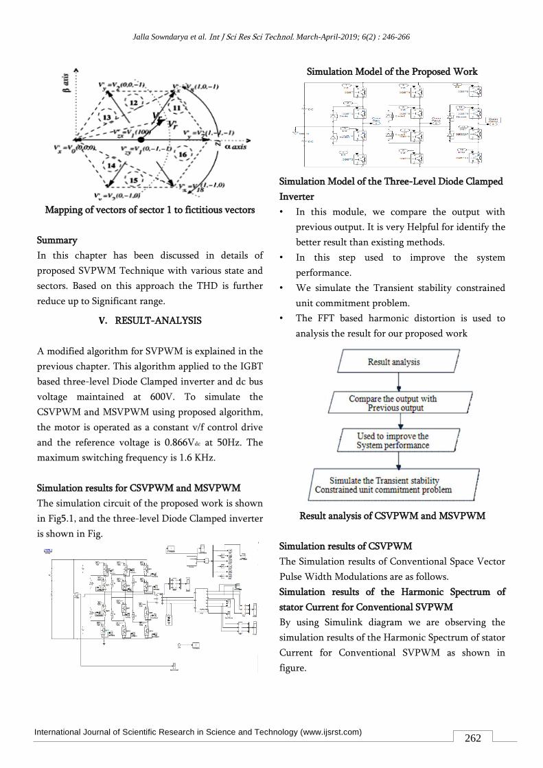
Selection of suitable switching sequences and states
Consider the above things we can easily identify
suitable switching sequences of out process.
International Journal of Scientific Research in Science and Technology (www.ijsrst.com)
Jalla Sowndarya et al. Int J Sci Res Sci Technol. March-April-2019; 6(2) : 246-266
262
Mapping of vectors of sector 1 to fictitious vectors
Summary
In this chapter has been discussed in details of
proposed SVPWM Technique with various state and
sectors. Based on this approach the THD is further
reduce up to Significant range.
V. RESULT-ANALYSIS
A modified algorithm for SVPWM is explained in the
previous chapter. This algorithm applied to the IGBT
based three-level Diode Clamped inverter and dc bus
voltage maintained at 600V. To simulate the
CSVPWM and MSVPWM using proposed algorithm,
the motor is operated as a constant v/f control drive
and the reference voltage is 0.866Vdc at 50Hz. The
maximum switching frequency is 1.6 KHz.
Simulation results for CSVPWM and MSVPWM
The simulation circuit of the proposed work is shown
in Fig5.1, and the three-level Diode Clamped inverter
is shown in Fig.
Simulation Model of the Proposed Work
Simulation Model of the Three-Level Diode Clamped
Inverter
• In this module, we compare the output with
previous output. It is very Helpful for identify the
better result than existing methods.
• In this step used to improve the system
performance.
• We simulate the Transient stability constrained
unit commitment problem.
• The FFT based harmonic distortion is used to
analysis the result for our proposed work
Result analysis of CSVPWM and MSVPWM
Simulation results of CSVPWM
The Simulation results of Conventional Space Vector
Pulse Width Modulations are as follows.
Simulation results of the Harmonic Spectrum of
stator Current for Conventional SVPWM
By using Simulink diagram we are observing the
simulation results of the Harmonic Spectrum of stator
Current for Conventional SVPWM as shown in
figure.
International Journal of Scientific Research in Science and Technology (www.ijsrst.com)
Jalla Sowndarya et al. Int J Sci Res Sci Technol. March-April-2019; 6(2) : 246-266
263
Harmonic Spectrum of Stator Current Waveforms
Simulation results of the Harmonic Spectrum of
Neutral Voltage for Conventional SVPWM
By using Simulink diagram we are observing the
simulation results of the Harmonic Spectrum of for
Neutral Voltage Conventional SVPWM as shown in
Fig.
Harmonic Spectrum of Neutral Voltage Waveforms
Simulation results of MSVPWM
The Simulation results of Modified Space Vector
Pulse Width Modulations are as follows.
Simulation results for Modified Space Vector Pulse
Width Modulation
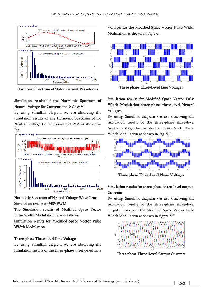
Three-phase Three-level Line Voltages
By using Simulink diagram we are observing the
simulation results of the three-phase three-level Line
Voltages for the Modified Space Vector Pulse Width
Modulation as shown in Fig 5.6.
Three phase Three-Level Line Voltages
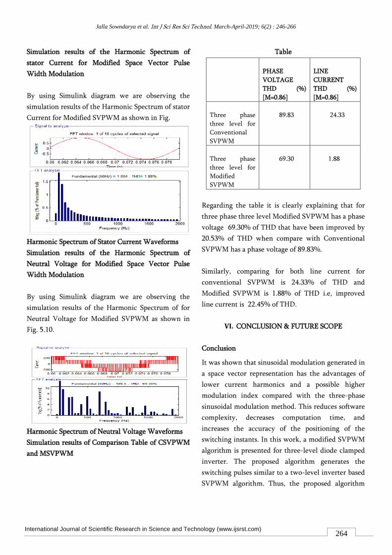
Simulation results for Modified Space Vector Pulse
Width Modulation three-phase three-level Neutral
Voltages
By using Simulink diagram we are observing the
simulation results of the three-phase three-level
Neutral Voltages for the Modified Space Vector Pulse
Width Modulation as shown in Fig. 5.7.
Three phase Three-Level Phase Voltages
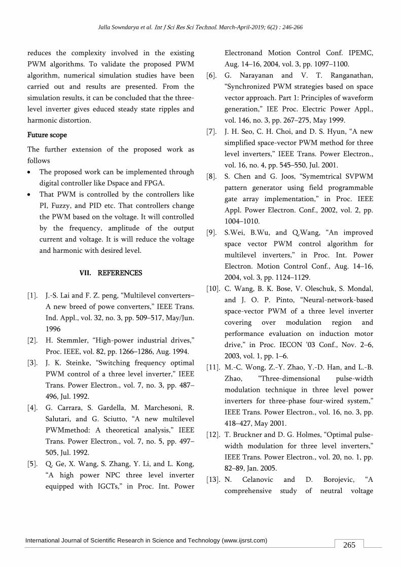
Simulation results for three-phase three-level output
Currents
By using Simulink diagram we are observing the
simulation results of the three-phase three-level
output Currents of the Modified Space Vector Pulse
Width Modulation as shown in figure 5.8.
Three phase Three-Level Output Currents
International Journal of Scientific Research in Science and Technology (www.ijsrst.com)
Jalla Sowndarya et al. Int J Sci Res Sci Technol. March-April-2019; 6(2) : 246-266
264
Simulation results of the Harmonic Spectrum of
stator Current for Modified Space Vector Pulse
Width Modulation
By using Simulink diagram we are observing the
simulation results of the Harmonic Spectrum of stator
Current for Modified SVPWM as shown in Fig.
Harmonic Spectrum of Stator Current Waveforms
Simulation results of the Harmonic Spectrum of
Neutral Voltage for Modified Space Vector Pulse
Width Modulation
By using Simulink diagram we are observing the
simulation results of the Harmonic Spectrum of for
Neutral Voltage for Modified SVPWM as shown in
Fig. 5.10.
Harmonic Spectrum of Neutral Voltage Waveforms
Simulation results of Comparison Table of CSVPWM
and MSVPWM
Table
PHASE
VOLTAGE
THD (%)
[M=0.86]
LINE
CURRENT
THD (%)
[M=0.86]
Three phase
three level for
Conventional
SVPWM
89.83
24.33
Three phase
three level for
Modified
SVPWM
69.30
1.88
Regarding the table it is clearly explaining that for
three phase three level Modified SVPWM has a phase
voltage 69.30% of THD that have been improved by
20.53% of THD when compare with Conventional
SVPWM has a phase voltage of 89.83%.
Similarly, comparing for both line current for
conventional SVPWM is 24.33% of THD and
Modified SVPWM is 1.88% of THD i.e, improved
line current is 22.45% of THD.
VI. CONCLUSION & FUTURE SCOPE
Conclusion
It was shown that sinusoidal modulation generated in
a space vector representation has the advantages of
lower current harmonics and a possible higher
modulation index compared with the three-phase
sinusoidal modulation method. This reduces software
complexity, decreases computation time, and
increases the accuracy of the positioning of the
switching instants. In this work, a modified SVPWM
algorithm is presented for three-level diode clamped
inverter. The proposed algorithm generates the
switching pulses similar to a two-level inverter based
SVPWM algorithm. Thus, the proposed algorithm
International Journal of Scientific Research in Science and Technology (www.ijsrst.com)
Jalla Sowndarya et al. Int J Sci Res Sci Technol. March-April-2019; 6(2) : 246-266
265
reduces the complexity involved in the existing
PWM algorithms. To validate the proposed PWM
algorithm, numerical simulation studies have been
carried out and results are presented. From the
simulation results, it can be concluded that the three-
level inverter gives educed steady state ripples and
harmonic distortion.
Future scope
The further extension of the proposed work as
follows
• The proposed work can be implemented through
digital controller like Dspace and FPGA.
• That PWM is controlled by the controllers like
PI, Fuzzy, and PID etc. That controllers change
the PWM based on the voltage. It will controlled
by the frequency, amplitude of the output
current and voltage. It is will reduce the voltage
and harmonic with desired level.
VII. REFERENCES
[1]. J.-S. Lai and F. Z. peng, “Multilevel converters–
A new breed of powe converters,” IEEE Trans.
Ind. Appl., vol. 32, no. 3, pp. 509–517, May/Jun.
1996
[2]. H. Stemmler, “High-power industrial drives,”
Proc. IEEE, vol. 82, pp. 1266–1286, Aug. 1994.
[3]. J. K. Steinke, “Switching frequency optimal
PWM control of a three level inverter,” IEEE
Trans. Power Electron., vol. 7, no. 3, pp. 487–
496, Jul. 1992.
[4]. G. Carrara, S. Gardella, M. Marchesoni, R.
Salutari, and G. Sciutto, “A new multilevel
PWMmethod: A theoretical analysis,” IEEE
Trans. Power Electron., vol. 7, no. 5, pp. 497–
505, Jul. 1992.
[5]. Q. Ge, X. Wang, S. Zhang, Y. Li, and L. Kong,
“A high power NPC three level inverter
equipped with IGCTs,” in Proc. Int. Power
Electronand Motion Control Conf. IPEMC,
Aug. 14–16, 2004, vol. 3, pp. 1097–1100.
[6]. G. Narayanan and V. T. Ranganathan,
“Synchronized PWM strategies based on space
vector approach. Part 1: Principles of waveform
generation,” IEE Proc. Electric Power Appl.,
vol. 146, no. 3, pp. 267–275, May 1999.
[7]. J. H. Seo, C. H. Choi, and D. S. Hyun, “A new
simplified space-vector PWM method for three
level inverters,” IEEE Trans. Power Electron.,
vol. 16, no. 4, pp. 545–550, Jul. 2001.
[8]. S. Chen and G. Joos, “Symemtrical SVPWM
pattern generator using field programmable
gate array implementation,” in Proc. IEEE
Appl. Power Electron. Conf., 2002, vol. 2, pp.
1004–1010.
[9]. S.Wei, B.Wu, and Q.Wang, “An improved
space vector PWM control algorithm for
multilevel inverters,” in Proc. Int. Power
Electron. Motion Control Conf., Aug. 14–16,
2004, vol. 3, pp. 1124–1129.
[10]. C. Wang, B. K. Bose, V. Oleschuk, S. Mondal,
and J. O. P. Pinto, “Neural-network-based
space-vector PWM of a three level inverter
covering over modulation region and
performance evaluation on induction motor
drive,” in Proc. IECON ’03 Conf., Nov. 2–6,
2003, vol. 1, pp. 1–6.
[11]. M.-C. Wong, Z.-Y. Zhao, Y.-D. Han, and L.-B.
Zhao, “Three-dimensional pulse-width
modulation technique in three level power
inverters for three-phase four-wired system,”
IEEE Trans. Power Electron., vol. 16, no. 3, pp.
418–427, May 2001.
[12]. T. Bruckner and D. G. Holmes, “Optimal pulse-
width modulation for three level inverters,”
IEEE Trans. Power Electron., vol. 20, no. 1, pp.
82–89, Jan. 2005.
[13]. N. Celanovic and D. Borojevic, “A
comprehensive study of neutral voltage
International Journal of Scientific Research in Science and Technology (www.ijsrst.com)
Jalla Sowndarya et al. Int J Sci Res Sci Technol. March-April-2019; 6(2) : 246-266
266
balancing problem in three level neutral point
clamped voltage source PWM inverters,” IEEE
Trans. Power Electron., vol. 15, no. 2, pp. 242–
249, Mar. 2002.
[14]. K. Yamanaka, A. M. Hava, H. Kirino, Y.
Tanaka, N. Koga, and T. Kume, “A novel
neutral point potential stabilization technique
using the information of output current
polarities and voltage vector,” IEEE Trans. Ind.
Appl., vol. 38, no. 6, pp. 1572–1580, Nov./Dec.
2002.
[15]. M. Botao, L. Congwei, Z. Yang, and L. Fahai,
“New SVPWM control scheme for three-phase
diode clamping multilevel inverter with
balanced dc voltages,” in IEEE IECON 2002
Conf., vol. 1, pp. 903–907.
[16]. H. L. Liu, N. S. Choi, and G. H. Cho, “DSP
based space vector PWM for three level
inverter with DC-link voltage balancing,” in
Proc. IEEE IECON 1991 Conf., vol. 2, pp. 197–
203.
[17]. S. Busquets-Monge, S. Somavilla, J. Bordonau,
and D. Boroyevich, “A novel modulation for
the comprehensive neutral-point balancing in
the three level NPC inverter with minimum
output switching-frequency ripple,” in Proc.
IEEE—PESC Conf., Jun. 20–25, 2004, vol. 6, pp.
4226–4232.
[18]. J. H. Seo and C. H. Choi, “Compensation for the
neutral-point potential variation in three level
space vector PWM,” in Proc. IEEE–APEC
Conf., 2001, vol. 2, pp. 1135–1140.
[19]. H. Zhang, A. Von Jouanne, S. Dai, A.
K.Wallace, and F.Wang, “Multilevel inverter
modulation schemes to eliminate common-
mode voltages,” IEEE Trans. Ind. Appl., vol. 36,
no. 6, pp. 1645–1653, Nov.-Dec. 2000.
[20]. A. R. Beig, “Application of three level voltage
source inverters to voltage fed and current fed
high power induction motor drives,” Ph.D.
dissertation, Indian Inst. Sci., Bangalore, India,
2004.
[21]. Reference Guide TMS320F/C240 DSP
Controllers: Peripheral Library and Specific
Devices Texas Instruments, 1999.
Cite this article as :
Jalla Sowndarya, M. Shekar, N. V. Vinay Kumar,
"Modified SVPWM Algorithm for Three Level VSI
With Synchronized and Symmetrical Waveforms",
International Journal of Scientific Research in
Science and Technology (IJSRST), Online ISSN :
2395-602X, Print ISSN : 2395-6011, Volume 6 Issue 2,
pp. 246-266, March-April 2019. Available at doi :
https://doi.org/10.32628/IJSRST196249
Journal URL : http://ijsrst.com/IJSRST196249


![The PWM Control of the Three-phase Induction Motor · [7] R. M Tallam, R. Naik, T. A. Nondah. A carrier based PWM scheme for neutral—point voltage balancing in three-level inverters](https://img.pdfslide.us/doc/110x75/6134dd0bdfd10f4dd73c00d7/the-pwm-control-of-the-three-phase-induction-motor-7-r-m-tallam-r-naik-t.jpg)