Embed Size (px)
Citation preview
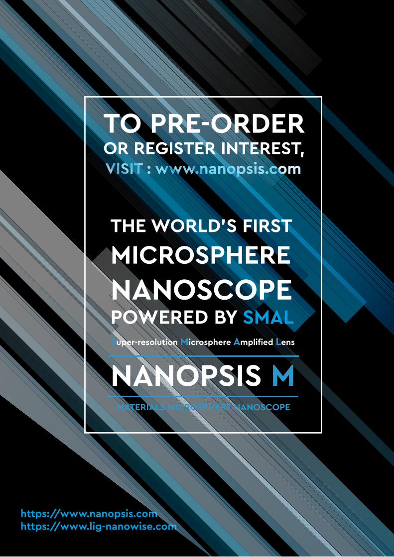
THE WORLD’S FIRST
MICROSPHERENANOSCOPE NANOSCOPE
POWERED BY SMALSuper-resolution Microsphere Amplified Lens
MA
TER
IALS
MIC
RO
SPH
ERE
NA
NO
SCO
PE
M
So we have developed SMON into SMAL (Super-resolution Microsphere Amplified Lens). The technology attaches to a white-light microscope, increasing its resolving limit to 70 -90 nm (depending on the sample) and potentially beyond.
SMON EVOLVEDThe basic principle of SMAL was first demonstrated in 2013 by Professor Lin Li, the chairman of LIG Nanowise. His work on SMON (Submerged Microsphere Optical Nanoscope) was published in the journal Light: Science and Applications in 2013. It was a nice demonstration of the power of microspheres, but SMON was never going to be repeatable, easy to use, or cost effective.
We specialise in nanotechnology - we are always using microscopes to view structures sub 200 nm in size. Sending samples to be imaged was slow, expensive, and took more effort than it was worth. We became tired of using SEM microscopes that were too large, loud, and too expensive to run in our own lab, and STED and STORM didn’t suit our requirements so we had a bright idea. STED and STORM have taken confocal microscopy into super-resolution - why not expand the range of wide-field optical microscopy? The result is the SMAL. It works in reflection mode in the wide-field, and allows you to add super-resolution imaging to your routine work. We aren’t proposing to replace SEMs, STED, or STORM- what SMAL offers is an easy, cost effective way, to examine samples beyond the range of standard optical microscopy. If you have ever used a white-light microscope you will be right at home using the NANOPSIS M.
WHY SMAL?
WHO WE ARE.NANOPSIS is the imaging brand of LIG Nanowise - a Manchester based start-up that specialises in the application of microsphere technology to solve the problems facing industry and R&D, based in the Manchester Science Park.
NANOPSIS MMATERIALS MICROSPHERE NANOSCOPE
WHAT IS SMAL?Super-resolution Microsphere Amplified Lens
Lorem ipsum
O
R
Paraxial Focal Length
ImagingPlane Position
White Light
THE THEORY
THE WORLD’S MOST POWERFUL OBJECTIVE LENS WITH X400MAGNIFICATION
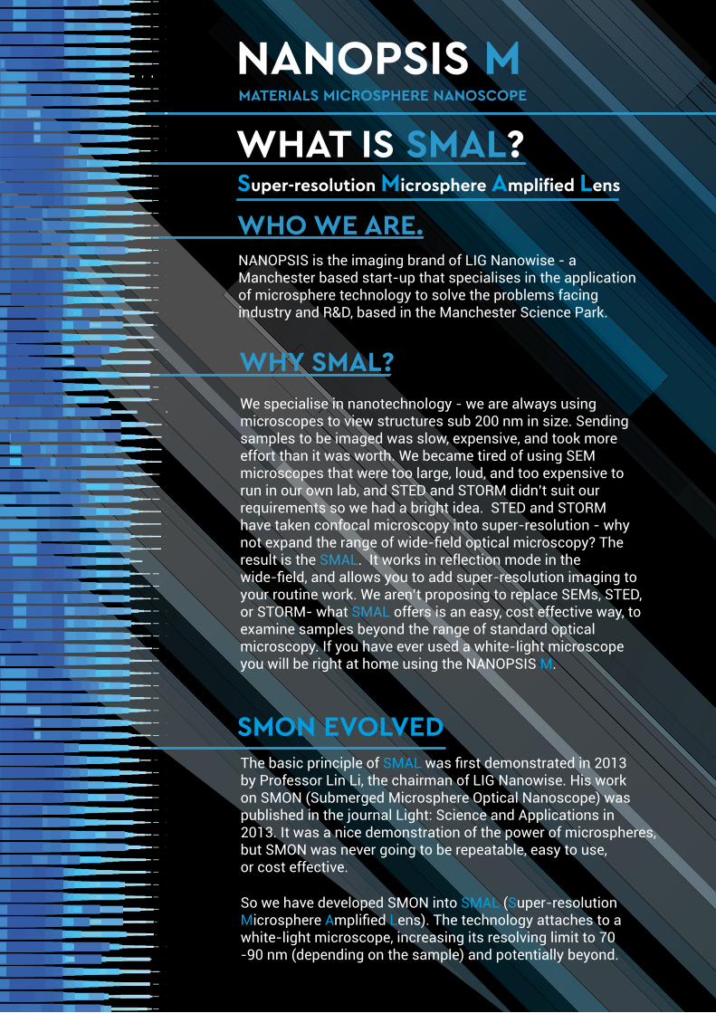
In 1896, Lord Rayleigh demonstrated the limitation of the lateral resolution in classical microscopy - two objects cannot be resolved if the distance between them is less than:
where λ is the wavelength of the incident light, and is NA the numerical aperture of the objective of the microscope. Then in air and with an objective lens with the maximal numerical aperture of 1, the resolution limit is around 200 nm.
Ernst Abbe made the same observation. When imaging gratings with different periods, he discovered that two elements of a particular grating cannot be resolved if their separation is less than:
From this equation, Abbe discovered that the resolution of an optical microscope is limited by diffraction and depends on the numerical aperture of the objective of microscope. Two objects can be resolved if the numerical aperture is big enough to collect the first order of diffraction of light diffracted by an object.
Beating this physical limitation became a challenge and led to the development of new microscopy technologies.
Powered by SMAL, the NANOPSIS M is our first non-contact optical imaging system, tailored for materials samples, that allows you to see the nanoscopic world as never before with x400 magnification.
Invented, developed, and built in Manchester UK, with the help of INNOVATE UK (grant number: 710761)
2 NAd = 1.22
Lorem ipsum
λ
2 NAd =
λ
MATERIALS MICROSPHERE NANOSCOPENANOPSIS M
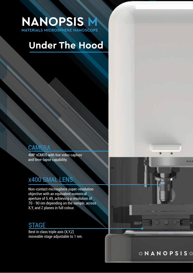
CAMERA4MP sCMOS with live video capture and time-lapse capability.
Under The Hood
Best in class triple axis (X,Y,Z) moveable stage adjustable to 1 nm.
STAGE
x400 SMAL LENS Non-contact microsphere super-resolution objective with an equivalent numerical aperture of 5.49, achieving a resolution of 70 - 90 nm depending on the sample, across X,Y, and Z planes in full colour.
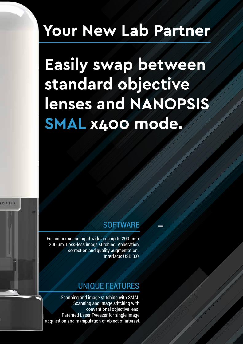
UNIQUE FEATURESScanning and image stitching with SMAL.
Scanning and image stitching with conventional objective lens.
Patented Laser Tweezer for single image acquisition and manipulation of object of interest.
SOFTWAREFull colour scanning of wide area up to 200 μm x
200 μm. Loss-less image stitching. Abberation correction and quality augmentation.
Interface: USB 3.0
Easily swap between standard objective lenses and NANOPSISSMAL x400 mode.
Your New Lab Partner
A FASTER SUPER-RESOLUTION WORKFLOW SEE MORE DETAIL THAN EVER BEFORE
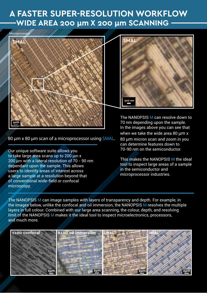
80 μm x 80 μm scan of a microprocessor using SMAL.
Our unique software suite allows you to take large area scans up to 200 μm x200 μm with a lateral resolution of 70 - 90 nm dependant upon the sample. This allows users to identify areas of interest across a large sample at a resolution beyond that of conventional wide-field or confocal microscopy.
The NANOPSIS M can resolve down to 70 nm depending upon the sample. In the images above you can see that when we take the wide area 80 μm x 80 μm micron scan and zoom in you can determine features down to 70-90 nm on the semiconductor. This makes the NANOPSIS M the ideal tool to inspect large areas of a sample in the semiconductor and microprocessor industries.
Microprocessor
The NANOPSIS M can image samples with layers of transparency and depth. For example, in the images below, unlike the confocal and oil immersion, the NANOPSIS M resolves the multiple layers in full colour. Combined with our large area scanning, the colour, depth, and resolvinglimit of the NANOPSIS M makes it the ideal tool to inspect microelectronics, processors, and much more.
4um
1µm
SMAL
-----------WIDE AREA 200 µm X 200 µm SCANNING --------------------------- -------------SEE DEPTH, COLOUR AND TRANSPARENCY-------------------------
x100 confocal
2µm
SMALSMAL
2µm 2µm
x100 oil immersion
2µm2µm
500 nm
SMALSMAL
2µm2µm
A FASTER SUPER-RESOLUTION WORKFLOW SEE MORE DETAIL THAN EVER BEFORE
SMAL1µm100x oil immersion
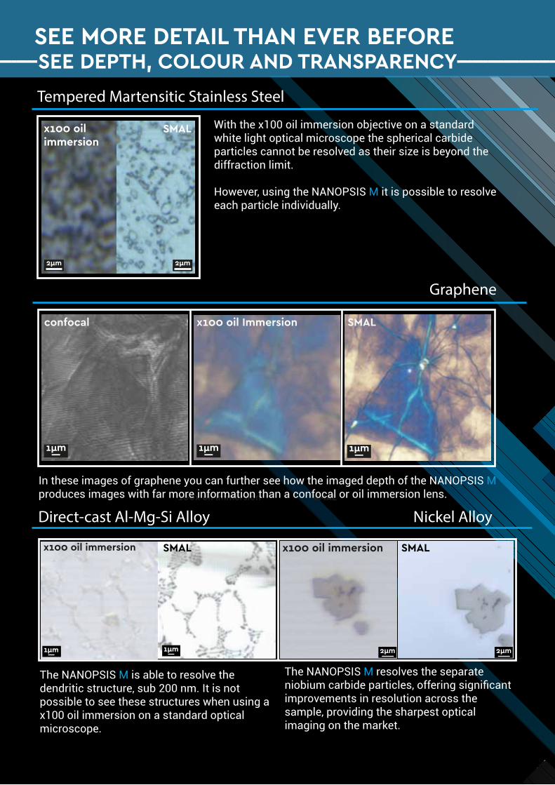
Tempered Martensitic Stainless Steel
1µm 2µm2µm
x100 oil immersion
100x oil immersion SMAL
1µm
100x oil immersion
1µm 1µm
1µm
SMAL
In these images of graphene you can further see how the imaged depth of the NANOPSIS M produces images with far more information than a confocal or oil immersion lens.
confocal x100 oil Immersion SMAL
1µm 1µm 1µm
Graphene
-----------WIDE AREA 200 µm X 200 µm SCANNING --------------------------- -------------SEE DEPTH, COLOUR AND TRANSPARENCY-------------------------
Direct-cast Al-Mg-Si Alloy Nickel Alloy
1µm
100x oil immersion1µm
x100 oil immersion
1µm
SMAL
1µm 2µm 2µm
SMALx100 oil immersion
The NANOPSIS M is able to resolve thedendritic structure, sub 200 nm. It is notpossible to see these structures when using a x100 oil immersion on a standard optical microscope.
The NANOPSIS M resolves the separateniobium carbide particles, offering significant improvements in resolution across thesample, providing the sharpest optical imaging on the market.
With the x100 oil immersion objective on a standard white light optical microscope the spherical carbideparticles cannot be resolved as their size is beyond the diffraction limit.
However, using the NANOPSIS M it is possible to resolve each particle individually.
SMAL
2µm
https://www.nanopsis.comhttps://www.lig-nanowise.com
VISIT : www.nanopsis.comhttp://www.nanopsis.com
TO PRE-ORDER OR REGISTER INTEREST,
THE WORLD’S FIRST
MICROSPHERENANOSCOPE NANOSCOPE
POWERED BY SMALSuper-resolution Microsphere Amplified Lens
MATERIALS MICROSPHERE NANOSCOPE
NANOPSIS M
http://www.nanopsis.com
TECHNOLOGY AND SALES GUIDE
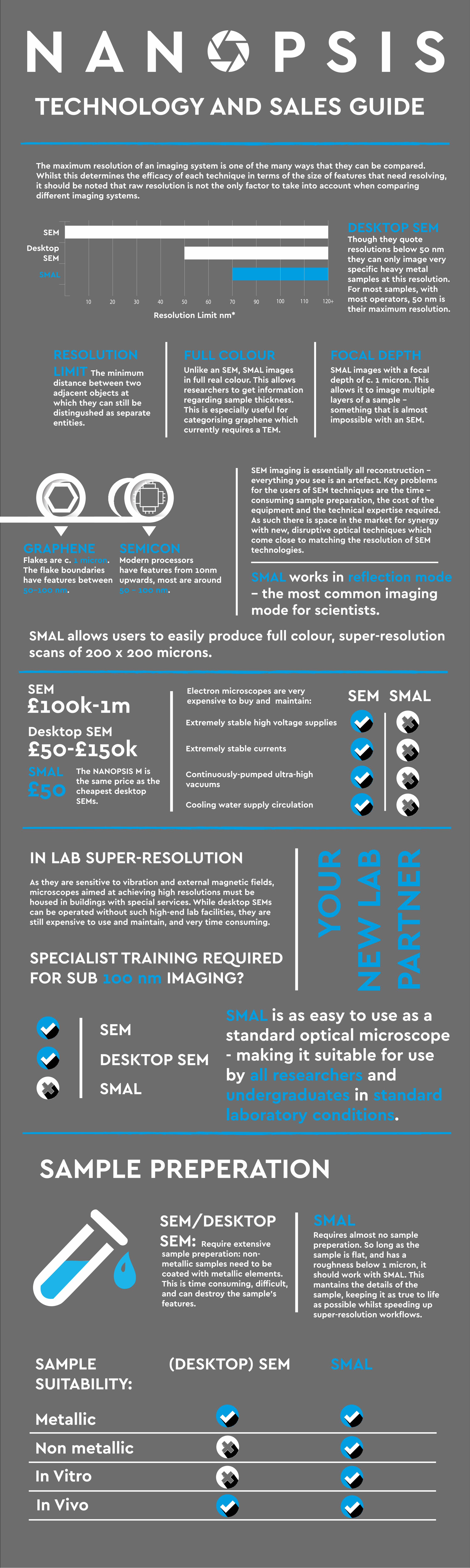
10 20 30 40 50 60 70 90 100 110 120+
The maximum resolution of an imaging system is one of the many ways that they can be compared. Whilst this determines the efficacy of each technique in terms of the size of features that need resolving, it should be noted that raw resolution is not the only factor to take into account when comparing different imaging systems.
RESOLUTIONLIMIT The minimumdistance between two adjacent objects atwhich they can still be distingushed as separateentities.
DESKTOP SEMThough they quote resolutions below 50 nmthey can only image very specific heavy metal samples at this resolution. For most samples, with most operators, 50 nm istheir maximum resolution.
FOCAL DEPTH
SEM
DesktopSEM
SMAL
Resolution Limit nm*
£100k-1m
£50
£50-£150k The NANOPSIS M is the same price as thecheapest desktop SEMs.
Electron microscopes are very expensive to buy and maintain:
SEM
Desktop SEM
SMAL
GRAPHENEFlakes are c. 1 micron.The flake boundaries have features between50–100 nm.
SEMICONModern processorshave features from 10nmupwards, most are around50 – 100 nm.
Unlike an SEM, SMAL imagesin full real colour. This allowsresearchers to get informationregarding sample thickness. This is especially useful forcategorising graphene which currently requires a TEM.
FULL COLOURSMAL images with a focal depth of c. 1 micron. Thisallows it to image multiplelayers of a sample – something that is almost impossible with an SEM.
SEM SMAL
Extremely stable high voltage supplies
Extremely stable currents
Continuously-pumped ultra-high vacuums
Cooling water supply circulation
IN LAB SUPER-RESOLUTIONAs they are sensitive to vibration and external magnetic fields, microscopes aimed at achieving high resolutions must be housed in buildings with special services. While desktop SEMs can be operated without such high-end lab facilities, they are still expensive to use and maintain, and very time consuming. Y
OU
RN
EW L
AB
PAR
TN
ER
SPECIALIST TRAINING REQUIRED FOR SUB 100 nm IMAGING?
SEM
DESKTOP SEM
SMAL
SMAL is as easy to use as a standard optical microscope - making it suitable for use by all researchers and undergraduates in standardlaboratory conditions.
SEM imaging is essentially all reconstruction – everything you see is an artefact. Key problems for the users of SEM techniques are the time –consuming sample preparation, the cost of the equipment and the technical expertise required. As such there is space in the market for synergy with new, disruptive optical techniques which come close to matching the resolution of SEM technologies.
SAMPLE PREPERATION
SEM/DESKTOPSEM:
(DESKTOP) SEM
Require extensive sample preperation: non-metallic samples need to be coated with metallic elements. This is time consuming, difficult, and can destroy the sample’s features.
SMAL
SMAL
Requires almost no sample preperation. So long as the sample is flat, and has a roughness below 1 micron, it should work with SMAL. This mantains the details of the sample, keeping it as true to life as possible whilst speeding up super-resolution workflows.
SAMPLE SUITABILITY:
Metallic
Non metallic
In Vivo
In Vitro
SMAL works in reflection mode – the most common imaging mode for scientists.
SMAL allows users to easily produce full colour, super-resolutionscans of 200 x 200 microns.
NANOPSISispartofLIGNanowiseLtd.
Unit11William’sHouse,ManchesterSciencePark,Manchester,M156SE(+44)[email protected]
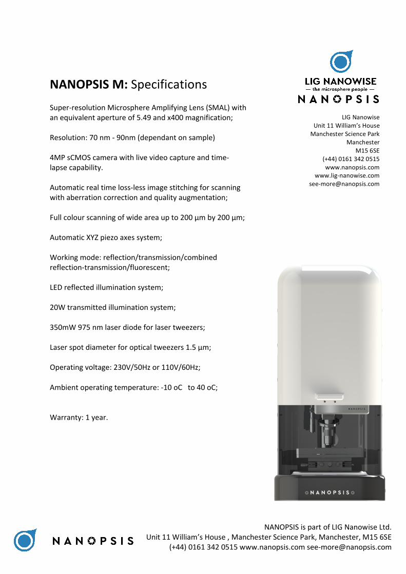
NANOPSISM:SpecificationsSuper-resolutionMicrosphereAmplifyingLens(SMAL)withanequivalentapertureof5.49andx400magnification;Resolution:70nm-90nm(dependantonsample)4MPsCMOScamerawithlivevideocaptureandtime-lapsecapability.Automaticrealtimeloss-lessimagestitchingforscanningwithaberrationcorrectionandqualityaugmentation;Fullcolourscanningofwideareaupto200μmby200μm;AutomaticXYZpiezoaxessystem;Workingmode:reflection/transmission/combinedreflection-transmission/fluorescent;LEDreflectedilluminationsystem;20Wtransmittedilluminationsystem;350mW975nmlaserdiodeforlasertweezers;Laserspotdiameterforopticaltweezers1.5μm;Operatingvoltage:230V/50Hzor110V/60Hz;Ambientoperatingtemperature:-10oCto40oC;Warranty:1year.
LIGNanowiseUnit11William’sHouseManchesterSciencePark
ManchesterM156SE
(+44)01613420515www.nanopsis.com
NANOPSISispartofLIGNanowiseLtd.
Unit11William’sHouse,ManchesterSciencePark,Manchester,M156SE(+44)[email protected]
NANOPSISM:FeaturesFullintegrationwithotherobjectivelensesforroutinework-easilyswapbetweenstandardobjectivelensesandNANOPSISSMALx400mode.TheNANOPSISMcanimagesampleswithlayersoftransparencyandhasahighdepthoffield.
NANOPSISM:ApplicationsItisidealforsemiconductoranalysisduetoitsfullcoloursuper-resolutioncapability,aswellasitsabilitytoimageacrossseverallayerswithdepthimaging;MaterialsscienceapplicationsinR&D-easilyswapbetweenregularobjectivesandsuper-resolutionx400SMALmode;Metallurgywherehighresolutionisrequired;Materialsqualitycontrolduetoitsrapidturnaroundtimeandabilitytobeusedasaregularroutineworkwhitelightmicroscopeaswellasasuper-resolutiontool.