Embed Size (px)
Citation preview

1
The world’s first industry-led consortium (501.c.6 non-profit) for the
manufacturing of advanced smart sensors and integrated devices

Industry
• Emerging Technologies
• Manufacturing
• Commercialization
Universities
• Universities in U.S.,
Europe, and Asia
• Funded research
• New ideas and approaches
• Partnered research capabilities
Government
• International
• State of Florida
• National research labs and agencies
• Attract joint funds
Suppliers
• Equipment
• Materials
• Software
• Industry R&D Labs & Programs
2
Innovation Networks & Open Innovation Programs That
Bring Industry, Universities And Governments Together
ICAMR: A New Era of International Collaboration

Programs
3
ICAMR is a 501.c.6 industry-led consortium that will provide open-innovation platforms that drive high-tech manufacturing through:
• Manufacturing scale-up of III-V and other novel materials ˗ Faster performance at lower power, wide band gap, high voltage and frequency
stability, chemical and extreme environment robustness,…
• Development of High Volume Manufacturing process equipment for next generation production lines & “Trusted Foundries”
• Integration of advanced devices and systems on 200 & 300 mm Si˗ Silicon is the ultimate integrator – can add virtually any device all on one carrier,
at any technology node
• 2.5 / 3-D device integration, and advanced packaging techniques
• Development of new test, metrology, reliability models for next generation materials
• Workforce development

The Promise of Smart Sensors
4
*
*
*
*- ICAMR initial target markets
Next disruptive market explosion will be “semiconductor-based” connected devices – led by advanced sensors and complimentary
photonic devices
& Flexible
Electronics
*
By 2020 over 75 billion devices will be connected by sensors
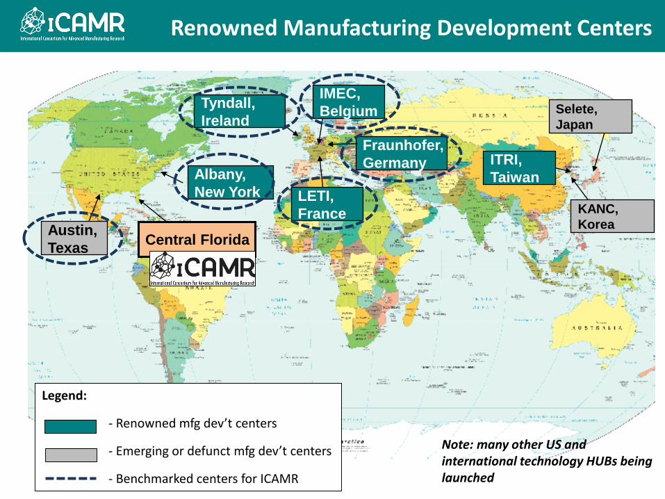
KANC,
Korea
Albany,
New York LETI,
France
IMEC,
Belgium Selete,
Japan
Renowned Manufacturing Development Centers
Austin,
Texas
Fraunhofer,
Germany
Central Florida
Note: many other US and international technology HUBs being launched
ITRI,
Taiwan
Legend:
- Renowned mfg dev’t centers
- Emerging or defunct mfg dev’t centers
- Benchmarked centers for ICAMR
Tyndall,
Ireland

1.ADVANCED MATERIALS
DEVELOPMENTIII-V and other novel materials deposited on
200mm/300mm Si substrates for advanced devices:
• Sensors• Photonic devices
• Integrated CMOS devices
3. SYSTEM
INTEGRATIONPackaging, test, and
systems development - including ultra-high
density 2.5/3-D interposers
Initial Focus: Smart Device Fabrication
6
Silicon
Advanced Materials
Transistors
Functionalized antenna
with wirelesscommunication
GaNGaAs
InGaAsInP
GaSbInGaN
2. DEVICE DEVELOPMENT
PILOT LINESDevice processing,
including novel techniques for device
personalization, functionalization, and
CMOS integration
OutsidePartners

III-V material advantages
Johnson’s and Keyes’s FM (Figure of Merritt) = performance of power transistors
1/Ron = close relationship to the power efficiency (lower operation costs, improved power density and size, reduced cost of ownership)

III-V scale-up W.S. during SEMICONKey Drivers and Highest Scored Challenges• Deposition/Growth:
– Defects, Equipment design, Temperature, Throughput
• Metrology:– Hybrid methods, Depth profiling, Gas purity, HVM capability
• Contamination control:– Dopants, Interface defects, Wet+dry etching, Monitoring
• Process: layers integration, generated defects, HVM CoO
• ESH: permits, abatement, chamber cleaning, training
• Facilities: hazardous materials, equip. segregation, alarms, flexibility
• Device integration: device nodes, thermal, flex. subst.
• Scalability: 200mm/300mm tool sets
• Standards: new SEMI committee, design rules, roadmap
• Others: educated workforce for III-V processing
87/14/2016 ICAMR Confidential

ICAMR Confidential
III-V Project Timeline
9
Jan-16 Feb-16 Mar-16 Apr-16 May-16 Jun-16 Jul-16 Aug-16 Sep-16 Oct-16 Nov-16 Dec-16
Develop defect free GaN on Si (111)
Develop defect free GaN on Si (100)
GaN device design and optimization
Fabricate GaN devices
Initial device testing
Demonstrate device performance
Reliability testing
Packaging
Jan-17 Feb-17 Mar-17 Apr-17 May-17 Jun-17 Jul-17 Aug-17 Sep-17 Oct-17 Nov-17 Dec-17
Develop defect free GaN on Si (100)
Develop backside CMOS fabrication
Tech Transfer to ICAMR facility
Initial device testing
Demonstrate device performance
Reliability testing
Packaging
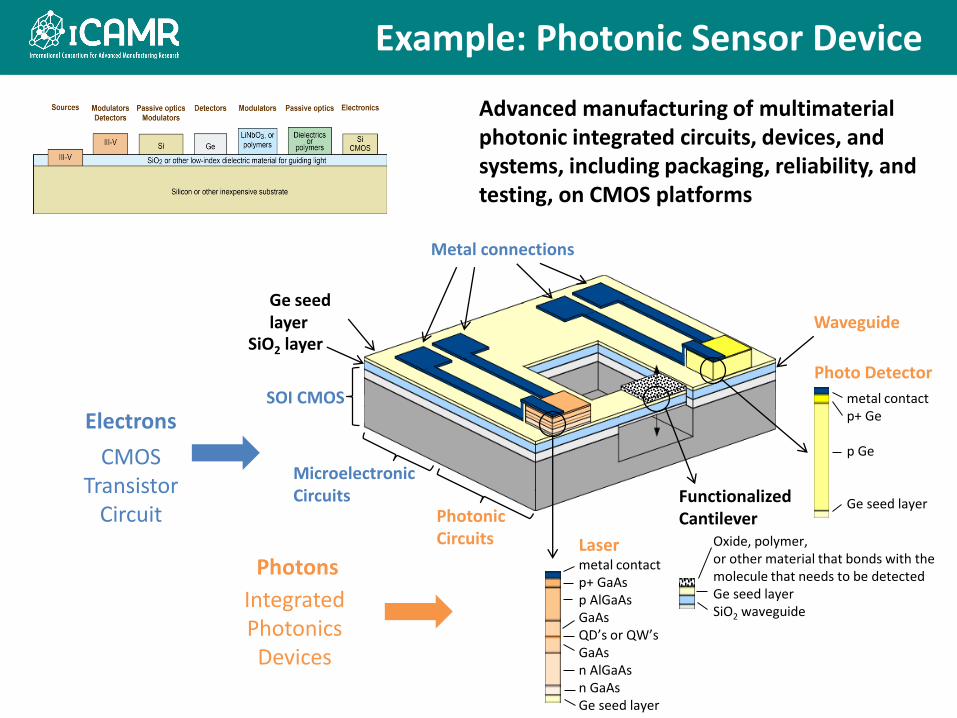
Example: Photonic Sensor Device
Advanced manufacturing of multimaterialphotonic integrated circuits, devices, and systems, including packaging, reliability, and testing, on CMOS platforms
CMOSTransistor
Circuit
IntegratedPhotonicsDevices
Electrons
Photons
SOI CMOS
Metal connections
Microelectronic Circuits
PhotonicCircuits
Photo Detector
Functionalized Cantilever
WaveguideSiO2 layer
Ge seed layer
metal contactp+ GaAsp AlGaAsGaAsQD’s or QW’sGaAsn AlGaAsn GaAsGe seed layer
Laser
metal contactp+ Ge
p Ge
Ge seed layer
Oxide, polymer, or other material that bonds with the molecule that needs to be detectedGe seed layerSiO2 waveguide

11
Device Manufacturing Development Model
Advanced Materials Development Line – key performance attributes:GaN, GaAs, InGaAs, InP, SiGe, Ge; others - CNT, SiC, C, Graphene, Magnetic (MOCVD/CVD/ALD dep. tools)
High sensitivity Low Power Harsh environments performance
ICAMR:III-V on Si
Outsource:Transistor arrays -Specified / mixed CMOS nodes
Interconnect and Personalization“Trusted Foundry”
Si
III-V / Novel Materials
ASIC (M1 – Mx)
Memory Logic
SensorsPhotonicsWireless
communication
Device / System Integration
Buffer layer
2.5D 3D
Interposer TSVFlip-chip bumps
µ bumpsDevice layer
Chip substrateMulti-Node (<22nm) CMOS, 3-D Integration Pilot-Line

12
ICAMR 2.5 / 3-D Interconnect PGM
ASIC
Flip-chip bumps
µ-bumps
InterposerTSVs
Logic
Memory
Memory
Memory
Package substrate
Sensor
• Device scale connections (TSV, Interposer, Bumps) at 1 x 10⁶ density
• Accelerate to achieve ITRS targets in the next 4 years
• Develop fabrication and assembly process for an order of magnitude
beyond current state-of-the-art 2.5D/3D Integration:
• Interposer pitch decreased from 45 to 5 mm
• TSV pitch reduced from 180 to 8 mm
• Depth from 100 to 50 mm
• Explore Additive Interposer Manufacturing – CNT/Dielectric Printing
- 3D Stacked IC
High Density Interposer

ICAMR Tool Roadmap
13
today 2016 2017 2018 2019
• Phase III – Packaging & TestPurchase and install advanced test, packaging, analytical, device libraries, and systems integration
• Phase II – Functionalization/PersonalizationPurchase & Install additional tool sets for specific device integration and support of industry driven program initiatives
• Phase I – Material Deposition – III-V on Silicon WaferPurchase & Install core tool set - flexible base, HVM platform for novel III-V and other material stacks on Si
• Phase 0Engage industry and define initial technology programs. Establish partners, define ICAMR tool sets and infrastructure needs. Processing will be done at partner labs/fabs.
• Phase IV – 2.5D/3D Purchase & install advanced 2.5-3D Interconnects / Si Interposer equipment set
• Phase VLaunch US industry and DOD “Trusted Foundry” operation
2020
Begin Tool Install
Phases To Move Left Based on Industry Demand
and Funding
ICAMR Confidential

Imec / ICAMR Partnership Tool Commonalities by Phases
14
Equipment TypePhase I
Materials Platforms
Phase II
Device integration
Phase III
Packaging & Test
Phase IV
2.5-3D Interconnect
Phase V
Back End
Sorter/Inspection * * * * *
Wet Clean * * * * *
Wet etch * * * * *HRXRD/XRR/XRD * * * * *AFM W/C-AFM CAPABILITY * * * * *VASE (SPECTROSCOPIC
ELIP)* * * * *
3D MICROSCOPE Contour * * * * *SURFACE DEFECT * * * * *PHOTOLUMINESCENCE * * *
CVD * * * * *
MOCVD * *
ALD * * * * *TXRF * *PROFILER, SURFACE ANAL * * * *FILM THICKNESS/DEFECT * * *
Litho (E-Beam) * * * *
Litho Track * * * *
PVD / Seed * * *
Furnace/RTP * * * *
PR Clean/Asher * * *
CMP-Metal * * *
CMP-IIIV * *
PECVD * *
Etch Dielectric * * *
Etch Metal * *
Etch Deep Si, TSV * * *
Adv Packaging & Test * * *
Plasma Etch * * *
Flip Chip * * *
Wafer Mounter * * *
Wire bonder * * *
Die Pick and Place * * *
Plate-Etch-Strip * * *
Wafer Bonding * * *
Wafer Grinder * * *
Laser / Saw Dicer * * *
Low K Dielectric Dep Spin/CVD * *
Litho (adv 248 or 193nm) * *
Cu Plating * *
Ta/TaN Barrier seed * *
Anneal * *
Dry & Wet Strip * *
TSV depth measurement * *
Temp Bonder * *
TEOS liner * *
Cu Plating ** (addt'l module) * *
Edge trim * *
Grind * *
Dry Etch * *
Wet Clean * *
LT ox/nit pass * *
Taping & Detaping * *
Reflow * *
Chipbonding & test * *
Die to Database Inspection *

Industry and the US Government are becoming very interested in the opportunities to leverage ICAMR’s infrastructure and resources. In the very near future, ICAMR plan to pursue a variety of Federal grants:
• Institutes of Manufacturing Innovation ($70M, multi-state consortium efforts) – Smart Manufacturing (DOE; FOA expected Q4 2015; award in 2016)– Advanced Materials Processing (agency and timing TBD)– Open Topic (NIST; 2016)
• DOD: Device / System Foundry Initiatives (Trusted Foundry)
• NIH – PRISMS (pediatric sensors)– Healthy, Independent Living (wearable sensors for geriatric care)– Bioengineering Research Partnership (with National Institute on Aging)
• DOE – ARPAe: harsh environment sensors (wireless rotary assets)– Next-generation manufacturing processes
• NSF – Smart and Connected Health (wearable sensors/assistive technology)– Cyber IT Research Infrastructure Programs
Federal Grant Engagement Proposals
For more info or to partner, please contact Andrea Wesser – [email protected] or 407-353-3469
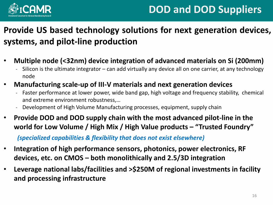
DOD and DOD Suppliers
16
Provide US based technology solutions for next generation devices,systems, and pilot-line production
• Multiple node (<32nm) device integration of advanced materials on Si (200mm)˗ Silicon is the ultimate integrator – can add virtually any device all on one carrier, at any technology
node
• Manufacturing scale-up of III-V materials and next generation devices˗ Faster performance at lower power, wide band gap, high voltage and frequency stability, chemical
and extreme environment robustness,…˗ Development of High Volume Manufacturing processes, equipment, supply chain
• Provide DOD and DOD supply chain with the most advanced pilot-line in the world for Low Volume / High Mix / High Value products – “Trusted Foundry”
(specialized capabilities & flexibility that does not exist elsewhere)
• Integration of high performance sensors, photonics, power electronics, RF devices, etc. on CMOS – both monolithically and 2.5/3D integration
• Leverage national labs/facilities and >$250M of regional investments in facility and processing infrastructure

• $138M from Osceola County
• Design/Build and equip 100,000 square foot center
• 20 acres plus in-kind support for power, water, and waste disposal
• $10M non-state and non-tuition funds to design and build center and start-up costs
• $7M in-kind for focused hires and resource support
• 30 year lease of center from Osceola County at $1 per year
• $1M for initial operating cost
• Up to $5M matching funds over five years for specific research projects
• $750K from USF, FIU and UF
• $2M State of Florida Quick Action Close Fund
Osceola County UCF FHTCC
Imec / ICAMR PartnershipStart-up Funding Partners
State of FL
17
Pre-Opening Start-up Funds Secured = $168M

Why Florida? – Business Opportunities
18

Florida / Regional – Business Opportunities
19
Aviation/Aerospace
★ AVIATION / AEROSPACE Home of Kennedy Space Center, Florida has 470+ companies ranging from aircraft and missiles to space exploration and manufacturing
✪ DEFENSE & HOMELAND SECURITYThe region is home to 20 major military installations, 3 unified combatant commands, 2 academic security institutes and nearly all of the nation’s leading contractors
■ OPTICS & PHOTONICS2,000+ specialists employed in some 100 companies in the region’s optics and photonics sector providing defense, communications and other industries with critical tools
✦ HEALTH LIFE SCIENCES1,100+ biotech, pharma & medical devices companies and 214 hospitals; including some of the nation’s most highly regarded research centers and health systems
20
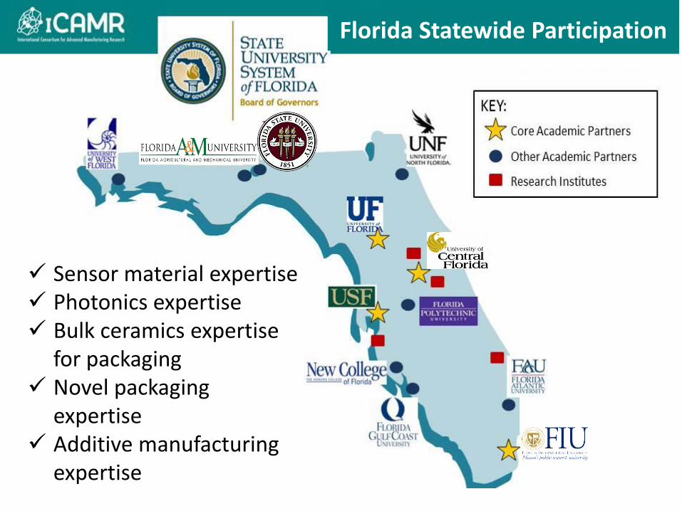
Sensor material expertise Photonics expertise Bulk ceramics expertise
for packaging Novel packaging
expertise Additive manufacturing
expertise
Florida Statewide Participation

Site: Kissimmee, Florida
21
ICAMR – 109,000 sq ft two level state-of-the-art R&D lab/fab facility - ~$140M• 30,000 sq ft of Class 1 – 1000 cleanroom• 22,500 sq ft of elevated waffle slab / sub fab• 10,000 sq ft of lab / office area (plus addition building support areas – services, loading dock,..)
• Site located on a new dedicated 350 acre research park• All utilities (electric, water, wastewater) available to site • Completion target is early 2017

22
DESIGN Duration
(mos.)
Start Finish
Programming 3 16-Mar-15 12-Jun-15
Conceptual Design 2 20-Apr-15 22-June-15
Advanced Schematic Design 1 6-July-15 10-Aug-15
Design Development 1.25 17-Aug-15 25-Aug-15
Construction Documents 5 17-Aug-15 19-Jan-16
CONSTRUCTION Duration
(mos.)
Start Finish
Site Construction (Early Site work & Foundations) 3.5 07-Oct-15 19-Jan-16
Shell Construction 8 14-Jan-16 16-Sep-16
Shell Dry-in 16-Feb-17
Equipment Start-up and Commissioning 7 29-July-16 21-Feb-17
Building Completion "Substantial" 21-Feb-17
Initial Tool Installation 1 3-Mar-17 31-Mar-17
Building Completion "Final" 31-Mar-17
Imec / ICAMR PartnershipFacilities Design and Construction

23
Facilities Layout• 20 acres and 100k ft2 ICAMR lab/fab to start
• 350 acres for high-tech campus and industry partners
Level 2Level 1
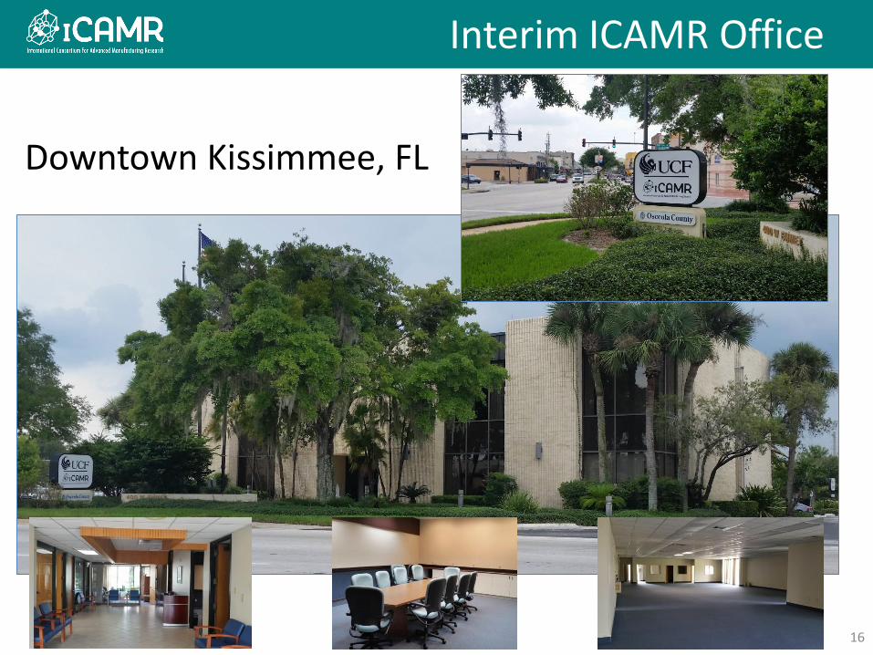
Downtown Kissimmee, FL
24
Interim ICAMR Office
16

25
Site Location
Downtown Orlando
Airport
Medical City
Kissimmee
Disney
UniversalStudios
Sea World
ICAMR
To the Beach
To Tampa
To Gainesville & Tallahassee
UCF
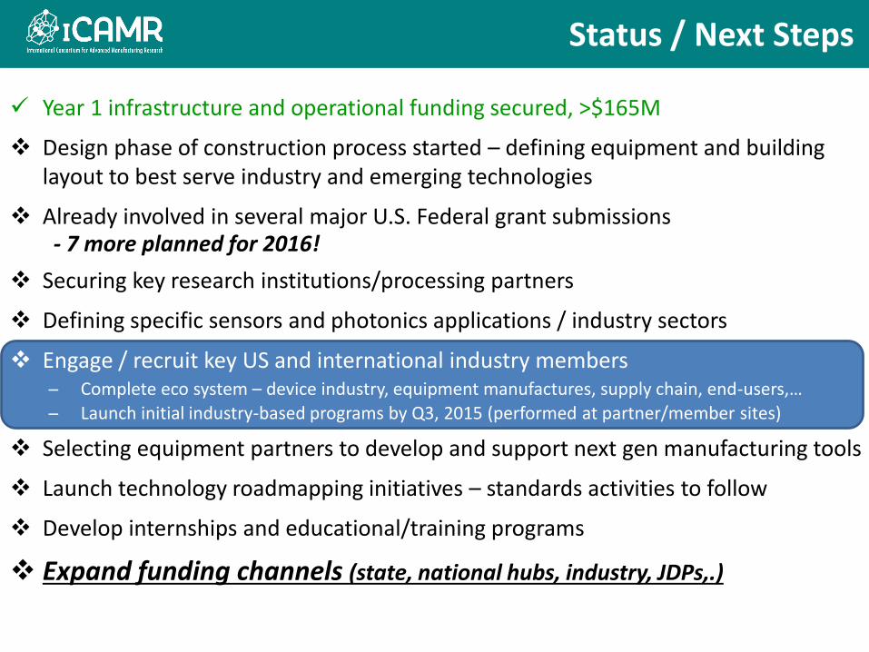
Year 1 infrastructure and operational funding secured, >$165M
Design phase of construction process started – defining equipment and building layout to best serve industry and emerging technologies
Already involved in several major U.S. Federal grant submissions - 7 more planned for 2016!
Securing key research institutions/processing partners
Defining specific sensors and photonics applications / industry sectors
Engage / recruit key US and international industry members Complete eco system – device industry, equipment manufactures, supply chain, end-users,…
Launch initial industry-based programs by Q3, 2015 (performed at partner/member sites)
Selecting equipment partners to develop and support next gen manufacturing tools
Launch technology roadmapping initiatives – standards activities to follow
Develop internships and educational/training programs
Expand funding channels (state, national hubs, industry, JDPs,.)
Status / Next Steps
CONTACT
[email protected] • 407-742-42543 Courthouse Square, 2nd Floor
Kissimmee, FL 34741
27
www.icamr.net

APPENDIX
28
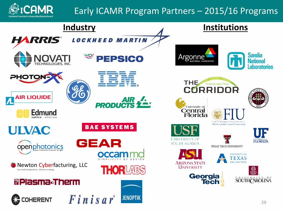
Early ICAMR Program Partners – 2015/16 Programs
29
InstitutionsIndustry

Building from Semiconductor Manufacturing Trajectory
2nd Gen
HKMG
2009
Si
FinFET
2012
32nm 22nm 14nm
Ge pMOS;
Si nMOS
2015
10nm
Ge
CMOS
2017
7nm 5nm
III-V
TFET
2021Ge
pMOS; III-
V nMOS
2019
Manufactured
Today
In
Development
3nm
D. K. Mohata VLSI 2012
???
2024
S. Banerjee 2009
30
ICAMR to build off III-V CMOS platforms for sensors/photonics and other advanced devices

Consortium Value Proposition
31
The Challenge
• Industry alignment
• Significant process, manufacturing, and technical design challenges
• Lack of industry collaboration, direction, and alignment around needs/challenges
• Access to leading-edge capabilities
• Testing and reliability
• Manufacturing cost
• System integration, technology commercialization, & workforce development
• Emerging technologies manufacturing scale-up challenges – small and large businesses
Collaborative Solutions
• Create industry roadmap and standards
• Collaborative R&D, access to equipment and facilities to speed process and product development
• Utilize & expand consortium model across entire value chain, develop a robust supplier industry around common needs
• Build / provide access to advanced manufacturing development facilities & labs
• Establish critical test, reliability, and analytical capabilities
• Improve manufacturing methods to enhance productivity and reduce costs
• Launch specialized programs and infrastructure to support industry needs and growth
• Leverage industry-government-university capabilities and resources through the consortium to provide manufacturing scale solutions

32
This model has been refined through years of testing:
• Multi-tiered programs and partnerships under one consortium structure
• Agility to adapt to changing needs
• Industry driven programs with high ROI – shared cost, risk, and value
• Development-friendly IP model promoting innovations across supply chain
Consortium / Collaboration Advantages
WIL
LIN
GN
ESS
TOC
OLL
AB
OR
ATE
HIGH
LOW
COMMON ISSUES & MANUFACTURINGCOLLABORATIONPRECOMPETITIVE
COMPETITIVE* COLLABORATIVE MFGR EXAMPLES:• New materials, equipment, & processes• Supplier/materials performance• Cost and materials models• Accelerated/improved testing• Metrology equipment (in-line/off-line)
*-ICAMR will conduct limited proprietary programs for Members

ICAMR’s Future Centers
33
Advanced Devices on Si -
Universal Smart Sensors:
- Sensor / Photonics Device
integration and prototyping
1) Adv Materials Development:
- Support a broad range of
Emerging Technologies
(BioMed, Environmental, Oil &
Gas, Aerospace/Defense,…)
2) Adv Personalization,
Functionalization, Test, and
Packaging Development Lines
- ICAMR focused industries/apps
3) Systems/Device integration
- Supporting product dev
MDF for Materials,Sensors, Packaging &
Testing
Manufacturing Hubs/Programs
- Industry/Technology-driven
initiatives
Next Generation
Manufacturing Pilot lines:
- Flexible Electronics
- Advanced Sys & Packaging
- Additive Manufacturing
- NEMS/MEMS/MOEMS
- Biomedical/Microfluidics
ManufacturingCompetitiveness
Centers
Advanced Energy Center
PV Programs
Next Gen PV (cSi & other)
Solar Systems & Power Elect
Smart Grid & Utility Solutions
Test & Certification (World Leader)
Energy Storage
Nanotechnology in Energy
Other renewables:
- Fuel cells
- Wind
- Marine current power
InternationalEmerging
TechnologiesEmerging Tech Programs
Cyber Security
Trusted Foundries
& device integrity
Healthcare Technologies
ESH
Nanotechnologies
Simulators & Models
Roadmaps & Standards
Joint University Centers
Workforce Development
ICAMR’s infrastructure is designed to support multiple emerging technology centers and industries
Phase I
This initiative has the potential to be a multi-billion $$$ operation!

Manufacturing Phase Transition
34
Phase I Processing
Phase IIProcessing
Phase III Processing
Industry Partners –Packaging/Systems
Industry Partners –Packaging/Systems
ICAMR –Packaging/System
Industry Partners –Functionalization and Personalization
ICAMR –Functionalization & Personalization
ICAMR
Industry Partners to process Ohmic contacts and passivation
ICAMR ICAMR
ICAMR to Deposit III-V Materials & Ge buffer Layer
ICAMR ICAMR
Si
n-InGaAlAs
n-InGaAs
p-InGaAlAsS D
Ge
Ohmic contactsTi, Ti/Pt, Al, W, Ta, Pd, AuMetallization/Sputtering/Ion implantation+annealing
Passivation layerSi3N4, SiNx, etc
Personalization / Functionalization(oxide, polymers or antibodies)
Baseline Photonics / Sensor Device

Full Partnership Opportunities as of Q3 2016
35
• Manufacturing technology roadmapping and standards
• Materials characterization, integration and manufacturing protocols
• Manufacturing development, prototyping and technology transfer - commercialization
• Process and metrology equipment development
• Technology production scale-up and cost modeling
• Environmental / Safety / Health challenges, and sustainability
• Certification/test/reliability – quality
• Policies/codes/permitting
• University, national labs, and international programs
• Member company application-specific support programs
• Workforce training - educational and internship programs

Manufacturing ConsortiumIntellectual property model
• Consortium owns all IP created by assignees and direct hires working on collaborative programs (except assignee created patents)
• IP is licensed to all members participating in a program on a nonexclusive, royalty-free basis
• Patented inventions created by assignee:– Are owned by the member that is the employer of the assignee
– Consortium members get nonexclusive, royalty-free license
• Inventions jointly created are jointly owned • Members’ patent license rights include right to make and
have made their own products and sublicense to customers • Partner and ICAMR will cooperate on publications and
conferences to benefit industry • Partner will own or have exclusive license to IP created in
privately funded program – IP license for ICAMR use will be negotiated as needed

37


![Study of transformation of defect states in GaN- and …...Lorenzo Rigutti. Study of transformation of defect states in GaN- and SiC-based materials and devices. Condensed Matter [cond-mat]](https://img.pdfslide.us/doc/110x75/5f0c67037e708231d435394a/study-of-transformation-of-defect-states-in-gan-and-lorenzo-rigutti-study.jpg)