Embed Size (px)
Citation preview

THE VLSI IMPLEMENTATION AND EVALUATION OF
AREA- AND ENERGY-EFFICIENT STREAMING MEDIA
PROCESSORS
A DISSERTATION
SUBMITTED TO THE DEPARTMENT OF ELECTRICAL ENGINEERING
AND THE COMMITTEE ON GRADUATE STUDIES
OF STANFORD UNIVERSITY
IN PARTIAL FULFILLMENT OF THE REQUIREMENTS
FOR THE DEGREE OF
DOCTOR OF PHILOSOPHY
Brucek Khailany
June 2003

c© Copyright by Brucek Khailany 2003
All Rights Reserved
ii

I certify that I have read this dissertation and that, in my opin-
ion, it is fully adequate in scope and quality as a dissertation
for the degree of Doctor of Philosophy.
William J. Dally(Principal Adviser)
I certify that I have read this dissertation and that, in my opin-
ion, it is fully adequate in scope and quality as a dissertation
for the degree of Doctor of Philosophy.
Mark Horowitz
I certify that I have read this dissertation and that, in my opin-
ion, it is fully adequate in scope and quality as a dissertation
for the degree of Doctor of Philosophy.
Teresa Meng
Approved for the University Committee on Graduate Stud-
ies.
iii

Abstract
Media applications such as image processing, signal processing, and graphics require tens
to hundreds of billions of arithmetic operations per second of sustained performance for
real-time application rates, yet also have tight power constraints in many systems. For
this reason, these applications often use special-purpose (fixed-function) processors, such
as graphics processors in desktop systems. These processors provide several orders of
magnitude higher performance efficiency (performance per unit area and performance per
unit power) than conventional programmable processors.
In this dissertation, we present the VLSI implementation and evaluation of stream pro-
cessors, which reduce this performance efficiency gap while retaining full programmability.
Imagine is the first implementation of a stream processor. It contains 48 32-bit arithmetic
units supporting floating-point and integer data-types organized into eight SIMD arithmetic
clusters. Imagine executes applications stream programs consisting of a sequence of com-
putation kernels operating on streams of data records. The prototype Imagine processor is
a 21-million transistor chip, implemented in a 0.15 micron CMOS process. At 232 MHz,
a peak performance of 9.3 GFLOPS is achieved while dissipating 6.4 Watts with a die size
measuring 16 mm on a side.
Furthermore, we extend these experimental results from Imagine to stream processors
designed in more area- and energy-efficient custom design methodologies and to future
VLSI technologies where thousands of arithmetic units on a single chip will be feasible.
Two techniques for increasing the number of arithmetic units in a stream processor are pre-
sented: intracluster and intercluster scaling. These scaling techniques are shown to provide
high performance efficiencies to tens of ALUs per cluster and to hundreds of arithmetic
clusters, demonstrating the viability of stream processing for many years to come.
iv

Acknowledgments
During the course of my studies at Stanford University, I have been fortunate to work with
a number of talented individuals. First and foremost, thanks goes to my research advisor,
Professor William J. Dally. Through his vision and leadership, Bill has always been an
inspiration to me and everyone else on the Imagine project. He also provided irreplacable
guidance for me when I needed to eventually find a dissertation topic. Professor Dally
provided me with the opportunity to take a leadership role on the VLSI implementation of
the Imagine processor, an invaluable experience for which I will always be grateful. I would
also like to thanks the other members of my reading committee, Professor Mark Horowitz
and Professor Teresa Meng, for their valuable feedback regarding the work described in
this dissertation and interactions over my years at Stanford.
The Imagine project was the product of the hard work of many graduate students in the
Concurrent VLSI Architecture group at Stanford. Most notably, I would like to thank Scott
Rixner, Ujval Kapasi, John Owens, and Peter Mattson. Together, we formed a team that
took the Imagine project from a research idea to a working silicon prototype. More recently,
Jung-Ho Ahn, Abhishek Das, and Ben Serebrin have helped with laboratory measurements.
Thanks also goes to all of the other team members who helped with the Imagine VLSI
implementation, including Jinyung Namkoong, Brian Towles, Abelardo Lopez-Lagunas,
Andrew Chang, Ghazi Ben Amor, and Mohamed Kilani.
I would also like to thank all of the other members of the CVA group at Stanford,
especially my officemates over the years: Ming-Ju Edward Lee, Li-Shiuan Peh, and Patrick
Chiang. Many thanks also goes to Pamela Elliot and Shelley Russell, the CVA group
administrators while I was a graduate student here.
The research described in this dissertation would not have been possible without the
v

generous funding provide by a number of sources. I would like to specifically thank the
Intel Foundation for a one-year fellowship in 2001-2002 to support this research. The
remainder of my time as a graduate student, I was supported by the Imagine project, which
was funded by the Defense Advanced Research Projects Agency under ARPA order E254
and monitored by the Army Intelligence Center under contract DABT63-96-C0037, by
ARPA order L172 monitored by the Department of the Air Force under contract F29601-
00-2-0085, by Intel Corporation, by Texas Instruments, and by the Interconnect Focus
Center Program for Gigascale Integration under DARPA Grant MDA972-99-1-0002.
Finally, I can not say enough about the support provided by my friends and family. My
parents, Asad (the first Dr. Khailany) and Laura, have been my biggest supporters and for
that I am forever grateful. Now that they will no longer be able to ask me when my thesis
will be done we will have to find a new subject to discuss on the telephone. My sister and
brother, Raygar and Sheilan, have always providing timely encouragement and advice. To
all of my friends and family members who have helped me in one way or another over the
years, I would like to say thanks.
vi

Contents
Abstract iv
Acknowledgments v
1 Introduction 1
1.1 Contributions . . . . . . . . . . . . . . . . . . . . . . . . . . . . . . . . . 3
1.2 Outline . . . . . . . . . . . . . . . . . . . . . . . . . . . . . . . . . . . . 3
2 Background 5
2.1 Media Applications . . . . . . . . . . . . . . . . . . . . . . . . . . . . . . 5
2.1.1 Compute Intensity . . . . . . . . . . . . . . . . . . . . . . . . . . 6
2.1.2 Parallelism . . . . . . . . . . . . . . . . . . . . . . . . . . . . . . 7
2.1.3 Locality . . . . . . . . . . . . . . . . . . . . . . . . . . . . . . . . 8
2.2 VLSI Technology . . . . . . . . . . . . . . . . . . . . . . . . . . . . . . . 8
2.3 Media Processing . . . . . . . . . . . . . . . . . . . . . . . . . . . . . . . 9
2.3.1 Special-purpose Processors . . . . . . . . . . . . . . . . . . . . . . 10
2.3.2 Microprocessors . . . . . . . . . . . . . . . . . . . . . . . . . . . 11
2.3.3 Digital Signal Processors and Programmable Media Processors . . 13
2.3.4 Vector Microprocessors . . . . . . . . . . . . . . . . . . . . . . . 13
2.3.5 Chip Multiprocessors . . . . . . . . . . . . . . . . . . . . . . . . . 14
2.4 Stream Processing . . . . . . . . . . . . . . . . . . . . . . . . . . . . . . . 15
2.4.1 Stream Programming . . . . . . . . . . . . . . . . . . . . . . . . . 15
2.4.2 Stream Architecture . . . . . . . . . . . . . . . . . . . . . . . . . 16
2.4.3 Stream Processing Related Work . . . . . . . . . . . . . . . . . . . 20
vii

2.4.4 VLSI Efficiency of Stream Processors . . . . . . . . . . . . . . . . 21
3 Imagine: Microarchitecture and Circuits 26
3.1 Instruction Set Architecture . . . . . . . . . . . . . . . . . . . . . . . . . . 27
3.1.1 Stream-Level ISA . . . . . . . . . . . . . . . . . . . . . . . . . . 27
3.1.2 Kernel-Level ISA . . . . . . . . . . . . . . . . . . . . . . . . . . . 28
3.1.3 Kernel Instruction Format . . . . . . . . . . . . . . . . . . . . . . 31
3.2 Microarchitecture . . . . . . . . . . . . . . . . . . . . . . . . . . . . . . . 31
3.2.1 Microcontroller . . . . . . . . . . . . . . . . . . . . . . . . . . . . 32
3.2.2 Arithmetic Clusters . . . . . . . . . . . . . . . . . . . . . . . . . . 34
3.2.3 Kernel Execution Pipeline . . . . . . . . . . . . . . . . . . . . . . 36
3.2.4 Stream Register File . . . . . . . . . . . . . . . . . . . . . . . . . 39
3.2.5 SRF Pipeline . . . . . . . . . . . . . . . . . . . . . . . . . . . . . 39
3.2.6 Streaming Memory System . . . . . . . . . . . . . . . . . . . . . 40
3.2.7 Network Interface . . . . . . . . . . . . . . . . . . . . . . . . . . 41
3.2.8 Stream Controller . . . . . . . . . . . . . . . . . . . . . . . . . . . 42
3.3 Arithmetic Cluster Function Units . . . . . . . . . . . . . . . . . . . . . . 43
3.3.1 ALU Unit . . . . . . . . . . . . . . . . . . . . . . . . . . . . . . . 43
3.3.2 MUL Unit . . . . . . . . . . . . . . . . . . . . . . . . . . . . . . 46
3.3.3 DSQ Unit . . . . . . . . . . . . . . . . . . . . . . . . . . . . . . . 49
3.3.4 SP Unit . . . . . . . . . . . . . . . . . . . . . . . . . . . . . . . . 50
3.3.5 COMM Unit . . . . . . . . . . . . . . . . . . . . . . . . . . . . . 50
3.3.6 JB/VAL Unit . . . . . . . . . . . . . . . . . . . . . . . . . . . . . 50
3.4 Summary . . . . . . . . . . . . . . . . . . . . . . . . . . . . . . . . . . . 54
4 Imagine: Design Methodology 56
4.1 Schedule . . . . . . . . . . . . . . . . . . . . . . . . . . . . . . . . . . . . 57
4.2 Design Methodology Background . . . . . . . . . . . . . . . . . . . . . . 57
4.3 Imagine Design Methodology . . . . . . . . . . . . . . . . . . . . . . . . 59
4.4 Imagine Implementation Results . . . . . . . . . . . . . . . . . . . . . . . 64
4.5 Imagine Clocking Methodology . . . . . . . . . . . . . . . . . . . . . . . 65
4.6 Imagine Verification Methodology . . . . . . . . . . . . . . . . . . . . . . 67
viii

5 Imagine: Experimental Results 69
5.1 Operating Frequency . . . . . . . . . . . . . . . . . . . . . . . . . . . . . 69
5.2 Power Dissipation . . . . . . . . . . . . . . . . . . . . . . . . . . . . . . . 73
5.3 Energy Efficiency . . . . . . . . . . . . . . . . . . . . . . . . . . . . . . . 76
5.4 Sustained Application Performance . . . . . . . . . . . . . . . . . . . . . 80
5.5 Summary . . . . . . . . . . . . . . . . . . . . . . . . . . . . . . . . . . . 81
6 Stream Processor Scalability: VLSI Costs 82
6.1 VLSI Cost Models . . . . . . . . . . . . . . . . . . . . . . . . . . . . . . 84
6.1.1 Stream Processor Cost Models . . . . . . . . . . . . . . . . . . . . 86
6.2 VLSI Cost Evaluation . . . . . . . . . . . . . . . . . . . . . . . . . . . . . 92
6.2.1 Intracluster Scaling . . . . . . . . . . . . . . . . . . . . . . . . . . 92
6.2.2 Intercluster Scaling . . . . . . . . . . . . . . . . . . . . . . . . . . 93
6.2.3 Combined Scaling . . . . . . . . . . . . . . . . . . . . . . . . . . 94
6.3 Custom and Low-Power Stream Processors . . . . . . . . . . . . . . . . . 96
7 Stream Processor Scalability: Performance 104
7.1 Related Scalability Work . . . . . . . . . . . . . . . . . . . . . . . . . . . 105
7.2 Technology Trends . . . . . . . . . . . . . . . . . . . . . . . . . . . . . . 106
7.2.1 Memory Bandwidth . . . . . . . . . . . . . . . . . . . . . . . . . 106
7.2.2 Wire Delay . . . . . . . . . . . . . . . . . . . . . . . . . . . . . . 107
7.3 Performance Evaluation . . . . . . . . . . . . . . . . . . . . . . . . . . . . 111
7.3.1 Kernel Inner-Loop Performance . . . . . . . . . . . . . . . . . . . 111
7.3.2 Kernel Short Stream Effects . . . . . . . . . . . . . . . . . . . . . 123
7.3.3 Application Performance . . . . . . . . . . . . . . . . . . . . . . . 126
7.3.4 Bandwidth Hierarchy Scaling . . . . . . . . . . . . . . . . . . . . 130
7.4 Improving Intercluster and Intracluster Scalability . . . . . . . . . . . . . . 132
7.5 Scalability Summary . . . . . . . . . . . . . . . . . . . . . . . . . . . . . 136
8 Conclusions 137
8.1 Future Work . . . . . . . . . . . . . . . . . . . . . . . . . . . . . . . . . . 138
ix

Bibliography 141
x

List of Tables
2.1 Media Processor Efficiencies (Normalized to 0.13µ, 1.2 V) . . . . . . . . . 11
3.1 Kernel ISA - Part 1 . . . . . . . . . . . . . . . . . . . . . . . . . . . . . . 29
3.2 Kernel ISA - Part 2 . . . . . . . . . . . . . . . . . . . . . . . . . . . . . . 30
3.3 JB/VAL Operation for Conditional Output Streams . . . . . . . . . . . . . 51
3.4 Function Unit Area and Complexity . . . . . . . . . . . . . . . . . . . . . 54
4.1 Subchip statistics . . . . . . . . . . . . . . . . . . . . . . . . . . . . . . . 60
4.2 Imagine placement results . . . . . . . . . . . . . . . . . . . . . . . . . . 64
4.3 Imagine timing results . . . . . . . . . . . . . . . . . . . . . . . . . . . . 66
5.1 Energy-Efficiency Comparisons . . . . . . . . . . . . . . . . . . . . . . . 77
5.2 Energy-Delay Comparisons . . . . . . . . . . . . . . . . . . . . . . . . . . 79
5.3 Sustained Application Performance . . . . . . . . . . . . . . . . . . . . . 80
6.1 Building Block Areas, Energies, and Delays . . . . . . . . . . . . . . . . . 84
6.2 Scaling Coefficients . . . . . . . . . . . . . . . . . . . . . . . . . . . . . . 85
6.3 Kernel Inner Loop Characteristics . . . . . . . . . . . . . . . . . . . . . . 86
6.4 Scaling Cost Models . . . . . . . . . . . . . . . . . . . . . . . . . . . . . 89
6.5 Building block Areas, Energies, and Delays for ASIC, CUST, and LP . . . 97
6.6 ASIC, CUST, and LP performance efficiencies . . . . . . . . . . . . . . . 98
6.7 Technology Scaling Parameters . . . . . . . . . . . . . . . . . . . . . . . . 100
7.1 Kernels and Applications use for Performance Evaluation . . . . . . . . . . 112
7.2 Intercluster Scaling Performance Efficiency . . . . . . . . . . . . . . . . . 122
xi
List of Figures
2.1 A Stereo Depth Extractor . . . . . . . . . . . . . . . . . . . . . . . . . . . 6
2.2 Stereo depth extractor as a stream program . . . . . . . . . . . . . . . . . . 16
2.3 Stream Processor Block Diagram . . . . . . . . . . . . . . . . . . . . . . . 17
2.4 Arithmetic Cluster Block Diagram . . . . . . . . . . . . . . . . . . . . . . 18
3.1 Imagine Arithmetic Cluster . . . . . . . . . . . . . . . . . . . . . . . . . . 28
3.2 VLIW Instruction Format . . . . . . . . . . . . . . . . . . . . . . . . . . . 32
3.3 Microcontroller Block Diagram . . . . . . . . . . . . . . . . . . . . . . . 33
3.4 Function Unit Details . . . . . . . . . . . . . . . . . . . . . . . . . . . . . 35
3.5 Local Register File Implementation . . . . . . . . . . . . . . . . . . . . . 35
3.6 Kernel Execution Pipeline Diagram . . . . . . . . . . . . . . . . . . . . . 37
3.7 Stream Register File Block Diagram . . . . . . . . . . . . . . . . . . . . . 38
3.8 SRF Pipeline Diagram . . . . . . . . . . . . . . . . . . . . . . . . . . . . 40
3.9 Stream Controller Block Diagram . . . . . . . . . . . . . . . . . . . . . . 42
3.10 ALU Unit Block Diagram . . . . . . . . . . . . . . . . . . . . . . . . . . 45
3.11 Segmented Carry-Select Adder . . . . . . . . . . . . . . . . . . . . . . . . 46
3.12 MUL Unit Block Diagram . . . . . . . . . . . . . . . . . . . . . . . . . . 47
3.13 DSQ Unit Block Diagram . . . . . . . . . . . . . . . . . . . . . . . . . . . 49
3.14 Computing the COMM Source Index in the JB/VAL unit . . . . . . . . . . 53
4.1 Standard ASIC Design Methodology . . . . . . . . . . . . . . . . . . . . . 58
4.2 Tiled Region Design Methodology . . . . . . . . . . . . . . . . . . . . . . 61
4.3 Tiled Region Floorplanning Details . . . . . . . . . . . . . . . . . . . . . 63
4.4 Asynchronous FIFO Synchronizer . . . . . . . . . . . . . . . . . . . . . . 67
xii

5.1 Die Photograph . . . . . . . . . . . . . . . . . . . . . . . . . . . . . . . . 70
5.2 Measured Operating Frequency . . . . . . . . . . . . . . . . . . . . . . . . 71
5.3 Measured Ring Delay . . . . . . . . . . . . . . . . . . . . . . . . . . . . . 72
5.4 Measured Core Power Dissipation . . . . . . . . . . . . . . . . . . . . . . 74
5.5 Csw distribution during Active Operation . . . . . . . . . . . . . . . . . . . 75
5.6 Measured Energy Efficiency . . . . . . . . . . . . . . . . . . . . . . . . . 76
6.1 Scalable Grid Floorplan . . . . . . . . . . . . . . . . . . . . . . . . . . . . 87
6.2 Intracluster Switch Floorplan . . . . . . . . . . . . . . . . . . . . . . . . . 91
6.3 Area of Intracluster Scaling . . . . . . . . . . . . . . . . . . . . . . . . . . 92
6.4 Energy of Intracluster Scaling . . . . . . . . . . . . . . . . . . . . . . . . 93
6.5 Area of Intercluster Scaling . . . . . . . . . . . . . . . . . . . . . . . . . . 94
6.6 Energy of Intercluster Scaling . . . . . . . . . . . . . . . . . . . . . . . . 95
6.7 Area of Combined Scaling . . . . . . . . . . . . . . . . . . . . . . . . . . 95
6.8 Effect of Technology Scaling on Die Area and Power Dissipation . . . . . . 101
6.9 Effect of Technology Scaling on Energy Efficiency . . . . . . . . . . . . . 102
7.1 Worst-case Switch Delay with Intracluster Scaling . . . . . . . . . . . . . . 108
7.2 Worst-case Switch Delay with Intercluster Scaling . . . . . . . . . . . . . . 109
7.3 Intracluster Scaling with no Loop Transformations . . . . . . . . . . . . . 113
7.4 Intracluster Scaling with Software Pipelining . . . . . . . . . . . . . . . . 116
7.5 Intracluster Scaling with Software Pipelining and Loop Unrolling . . . . . 118
7.6 Inner-Loop Performance per Area with Intracluster Scaling . . . . . . . . . 120
7.7 Intercluster Kernel Speedup . . . . . . . . . . . . . . . . . . . . . . . . . . 121
7.8 Kernel Short Stream Effects . . . . . . . . . . . . . . . . . . . . . . . . . 124
7.9 Application Performance . . . . . . . . . . . . . . . . . . . . . . . . . . . 127
7.10 Application Cycles with Intercluster Scaling (N=5) . . . . . . . . . . . . . 129
7.11 Bandwidth Hierarchy with Intercluster Scaling (N=5) . . . . . . . . . . . . 131
7.12 Intercluster Switch Locality with 8x8 Cluster Grid Floorplan . . . . . . . . 134
7.13 Limited-Connectivity Inercluster Switch for 8x8 Cluster Floorplan . . . . . 135
xiii

Chapter 1
Introduction
Computing devices and applications have recently emerged to interface with, operate on,
and process data from real-world samples classified as media. As media applications oper-
ating on these data-types have come to the forefront, the design of processors optimized to
operate on these applications have emerged as an important research area. Traditional mi-
croprocessors have been optimized to execute applications from desktop computing work-
loads. Media applications are a workload with significantly different characteristics, mean-
ing that the potential for large improvements in performance, cost, and power efficiency
can be achieved by improving media processors.
Media applications include workloads from the areas of signal processing, image pro-
cessing, video encoding and decoding, and computer graphics. These workloads require a
large and growing amount of arithmetic performance. For example, many current computer
graphics and image processing applications in desktop systems require tens to hundreds of
billions of arithmetic operations per second for real-time performance [Rixner, 2001]. As
scene complexity, screen resolutions, and algorithmic complexity continues to grow, this
demand for absolute performance will continue to increase. Similar examples of large and
growing performance requirements can be drawn in the other application areas, such as
the need for higher communication bandwidth rates in signal processing and higher video
quality in video encoding and decoding algorithms. As a result, media processors must be
designed to provide large amounts of absolute performance.
While high performance is necessary to meet the computational requirements of media
1
CHAPTER 1. INTRODUCTION 2
applications, many media processors will need to be deployed in mobile systems and other
systems where cost and power consumption is a key concern. For this reason, low power
consumption and high energy efficiency, or high performance per unit power (low aver-
age energy dissipated per arithmetic operation), must be a key design goal for any media
processor.
Fixed-function processors have been able to provide both high performance and good
energy-efficiency when compared to their programmable counterparts on media applica-
tions. For example, the Nvidia Geforce3 [Montrym and Moreton, 2002; Malachowsky,
2002], a recent graphics processor, provides 1.2 Teraops per second of peak performance
at 12 Watts for an energy-efficiency of 10 picoJoules per operation. In comparison, pro-
grammable digital signal processors and microprocessors are several orders of magnitude
worse in absolute performance and in energy efficiency. However, programmability is a key
requirement in many systems where algorithms are too complex or change too rapidly to
be built into fixed-function hardware. Using programmable rather than fixed-function pro-
cessors also enables fast time-to-market. Finally, the cost of building fixed-function chips
is growing significantly in deep sub-micron technologies, meaning that programmable so-
lutions also have an inherent cost advantage since a single programmable chip can be used
in many different systems. For these reasons, a programmable media processor which can
provide the performance and energy efficiency of fixed-function media processors is desir-
able.
Stream processors have recently been proposed as a solution that can provide all three
of the above: performance, energy efficiency, and programmability. In this dissertation,
the design and evaluation of a prototype stream processor, called Imagine is presented.
This 21-million transistor processor is implemented in a 5-level metal 0.15 micron CMOS
technology with a die size measuring 16 millimeters on a side. At 232 MHz, a peak per-
formance of 9.3 GFLOPS is achieved while dissipating 6.4 Watts. Furthermore, in future
VLSI technologies, the scalability of stream processors to Teraops per second of peak per-
formance is demonstrated.

CHAPTER 1. INTRODUCTION 3
1.1 Contributions
This dissertation makes several contributions to the fields of computer architecture and
media processing:
• The design and evaluation of the Imagine stream processor. This is the first VLSI
implementation of a stream architecture and provides experimental verification to
the VLSI feasibility and performance of stream processors.
• Analysis on the performance efficiency of stream processors. This analysis demon-
strates the potential for providing high performance per unit area and high perfor-
mance per unit power when compared to other media processor architectures.
• Analytical models for the area, power, and delay of key components of a stream
processor. These models are used to demonstrate the scalability of stream processors
to thousands of arithmetic units in future VLSI technologies.
• An analysis of the performance of media applications as the number of arithmetic
units per stream processor are increased. This analysis provides insights into the
available parallelism in media applications and explores the tradeoffs in area, power,
and performance for different methods of scaling to large numbers of arithmetic units
per stream processor.
1.2 Outline
Recently, media processing has gained attention in both commercial products and academic
research. The important recent trends in media processing are presented in Chapter 2. One
such trend which has gained prominence in the research community is stream processing.
In Chapter 2, we introduce and explain stream processing, which consists of a programming
model and architecture that enables high performance on media applications with fully-
programmable processors.
In order to explore the performance and efficiency of stream processing, a prototype
stream processor, Imagine, was designed and implemented in a modern VLSI technology.

CHAPTER 1. INTRODUCTION 4
In Chapter 3, the instruction set architecture, microarchitecture, and key arithmetic circuits
from Imagine are described. In Chapter 4, the design methodology is presented and finally,
in Chapter 5, experimental results are provided. Also in Chapter 5, the energy efficiency of
Imagine and a comparison to existing processors is presented.
This work on Imagine was then extended to study the scalability of stream processors
to future VLSI technologies when thousands of arithmetic units could fit on a single chip.
In Chapter 6, analytical models for the area, power, and delay of key components of a
stream processor are presented. These models are then used to explore how area and energy
efficiency scales with the number of arithmetic units. In Chapter 7, performance scalability
is studied by exploring the avaiable parallelism in media applications and by exploring the
tradeoffs between different methods of scaling.
Finally, conclusions and future work are presented in Chapter 8.

Chapter 2
Background
Media applications and media processors have recently become an active and important
area of research. In this chapter, background and previous work on media processing is
presented. First, media application characteristics and previous work on processors for
running these applications is presented. Then, stream processors are introduced. Stream
processors have recently been proposed as an architecture that exploits media application
characteristics to achieve better performance, area efficiency, and energy efficiency than
existing programmable processors.
2.1 Media Applications
Media applications are programs with real-time performance requirements that are used
to process audio, video, still images, and other data-intensive data. Example application
domains include image processing, computer-generated graphics, video encoding or de-
coding, and signal processing. As previous researchers have pointed out, these applications
share several important characteristics: compute intensity, parallelism, and locality [Rixner,
2001].
A flow-diagram representation of one such media application, a stereo depth extractor,
is shown graphically in Figure 2.1 [Kanade et al., 1996]. In this application, using two
images offset by a horizontal disparity as input from two cameras, each row from each
image is first filtered and then compared using a sum-of-absolute differences metric to
5

CHAPTER 2. BACKGROUND 6
ConvolutionFilter
ConvolutionFilter
Left Image
Center Image
Sum-of-Absolute
Differences
Depth Map
Figure 2.1: A Stereo Depth Extractor
estimate the disparity between objects in the images. From the disparity calculated at each
image pixel, the depth of objects in an image can be approximated. This stereo depth
extractor will be used to demonstrate the three important characteristics common to most
media applications.
2.1.1 Compute Intensity
The first important characteristic is compute intensity, meaning that media applications
require a high number of arithmetic operations per memory reference when compared to
traditional desktop applications. Rixner studied application characteristics of four media
applications: the stereo depth extractor presented above, a video encoder/decoder, a poly-
gon renderer, and a matrix QR decomposition [Rixner, 2001]. On the stereo depth extractor,
473.3 arithmetic operations in the convolution filter and sum-of-absolute difference calcu-
lations were required per inherent memory reference (input, output, and other global data
accesses). The other applications ranged between 57.9 and 155.3 arithmetic operations per
memory reference. In comparison, traditional desktop integer applications have ratios of
less than 2: arithmetic operations comprise between 2% and 50% of dynamically executed
instructions whereas memory loads and stores account for 15% to 80% of instructions in the
SPECint2000 benchmark suite [KleinOsowski et al., 2000]. This difference suggests that
architectures optimized for integer benchmarks such as general-purpose microprocessors
would not be as well-suited to media applications and vice versa.

CHAPTER 2. BACKGROUND 7
2.1.2 Parallelism
Not only do these applications require large numbers of arithmetic operations per memory
reference, but many of these arithmetic operations can be executed in parallel. This avail-
able parallelism in media applications can be classified into three categories: instruction-
level parallelism (ILP), data-level parallelism (DLP), and task-level parallelism (TLP).
The most plentiful parallelism in media applications is at the data level. DLP refers to
computation on different data elements occurring in parallel. Furthermore, DLP in media
applications can often be exploited with SIMD execution since the same computation is
typically applied to all data elements. For example, in the stereo depth extractor, all output
pixels in the depth map could theoretically be computed in parallel by the same fixed-
function hardware element since there are no dependencies between these pixels and the
computation required for every pixel is the same. Other media applications also contain
large degrees of DLP.
Some parallelism also is available at the instruction level. In the stereo depth extractor,
ILP refers to the parallel execution of individual arithmetic instructions in the convolution
filter or sum-of-absolute differences calculation. For example, the convolution filter com-
putes the product of a coefficient matrix with a sequence of pixels. This matrix-vector
product includes a number of multiplies and adds that could be performed in parallel. Such
fine-grained parallelism between individual arithmetic operations operating on one data el-
ement is classified as ILP and can be exploited in many media applications. As will be
shown later in Chapter 7, available ILP in media applications is usually limited to a few in-
structions per cycle due to dependencies between instructions. Although other researchers
have shown that out-of-order superscalar microprocessors are able to execute up to 4.2 in-
structions per cycle on some media benchmarks [Ranganathan et al., 1999], this is largely
due to DLP being converted to ILP with compiler or hardware techniques rather than the
true ILP that exists in these applications.
Finally, the stereo depth extractor and other media applications also contain task-level,
or thread-level, parallelism. TLP refers to different stages of a computation pipeline being
overlapped. For example, in the stereo depth extractor, there are four exeuction stages: load
image data, convolution filter, sum-of-absolute differences, and store output data. TLP is

CHAPTER 2. BACKGROUND 8
available in this application because these execution stages could be set up as a pipeline
where each stage concurrently processes different portions of the dataset. For example, a
pipeline could be set up where each stage operates on a different row: the fourth image rows
are loaded from memory, the convolution filter operates on the third rows, sum-of-absolute
differences is computed between the second rows, while the first output row is stored back
to memory. Note that ILP, DLP, and TLP are all orthogonal types of parallelism, meaning
that all three could theoretically be supported simultaneously.
2.1.3 Locality
In addition to compute intensity and parallelism, the other important media application
characteristic is locality of reference for data accesses. This locality can be classified into
kernel locality and producer-consumer locality. Kernel locality is temporal and refers to
reuse of coefficients or data during the execution of computation kernels such as the con-
volution filter. Producer-consumer locality is also a form of temporal locality that exists
between different stages of a computation pipeline or kernels. It refers to data which is pro-
duced, or written, by one kernel and consumed ,or read, by another kernel and is never read
again. This form of locality is seen very frequently in media applications [Rixner, 2001]. In
a traditional microprocessor, kernel locality would most often be captured in a register file
or a small first-level cache. Producer-consumer locality on the other hand is not as easily
captured by traditional cache hierarchies in microprocessors since it is not well-matched to
least-recently-used replacement policies typically utilized in caches.
2.2 VLSI Technology
Not only has the typical application domain for programmable processors shifted over the
last decade, the technology constraints of modern VLSI (Very Large Scale Integrated Cir-
cuits) has evolved as well. In the past, gates used for computation were the critical re-
source in VLSI design, but in modern technology, computation is cheap and communica-
tion between computational elements is expensive. For example, in the Imagine proces-
sor [Khailany et al., 2002], a single-precision floating-point multiply-accumulate unit in a

CHAPTER 2. BACKGROUND 9
0.18 µm technology measures 0.486 mm2 and dissipates 185 pJ per multiply (0.185 mW
per MHz). A thousand of these multipliers could fit on a single die in a 0.13 µm technology.
While arithmetic itself is cheap, handling the data and control communication between
arithmetic units is expensive. On-chip communication between such arithmetic units re-
quires storage and wires. Small distributed storage elements are not too expensive com-
pared to arithmetic. In the same 0.18 µm technology, a 16-word 32-bit, one-read-port
one-write-port SRAM which is 0.0234 mm2 and dissipates 15pJ per access cycle assum-
ing both ports are active. However, as additional ports are added to this memory, the area
cost increases significantly. Furthermore, the drivers and wires for a 32-bit 5 millimeter
bus dissipate 24 pJ per transfer on average [Ho et al., 2001]. If each multiply requires
three multi-ported memory accesses and three 5 millimeter bus transfers (two reads and
one write), then the cost of the communication is very similar to the cost of a multiply.
Architectures must therefore manage this communication effectively in order to keep its
area and energy costs from dominating the computation itself. Off-chip communication is
an even more critical resource, since there are only hundreds of pins available in large chips
today. In addition, each off-chip communication dissipates a lot of energy (typically over 1
nJ for a 32b transfer) when compared to arithmetic operations.
Although handling the cost of communication in modern VLSI technology is a chal-
lenge, media application characteristics are well-suited to take advantage of cheap com-
putation with highly distributed storage with local communications. Cheap computation
can be exploited with large numbers of arithmetic units to take advantage of both compute
intensity and parallelism in these applications. Furthermore, producer-consumer locality
can be exploited to keep communication local as much as possible, thereby minimizing
communication costs.
2.3 Media Processing
Processors can exploit application characteristics to provide both high performance and
more importantly, performance efficiency. High performance efficiency implies a high ra-
tio of performance per unit area, area efficiency, and a high ratio of performance per unit

CHAPTER 2. BACKGROUND 10
power, energy or power efficiency. These metrics are often more important than raw per-
formance in many media processing systems since higher area efficiency leads to low cost
and better manufacturability, both important in embedded systems. Energy efficiency im-
plies that for executing a fixed computation task, less energy from a power source such as a
battery is used, leading to longer battery life and lower packaging costs in mobile products.
In this section, we present previous work on fixed-function and programmable processors
for media applications, with data on both performance and performance efficiency.
2.3.1 Special-purpose Processors
Special-purpose, or fixed-function, processors directly map an application’s data-flow graph
into hardware and can therefore exploit important application characteristics. They contain
a large number of computation elements operating in parallel, exploiting both the compute
intensity and parallelism in media applications. These computation blocks are then con-
nected together by dedicated wires and memories, exploiting available producer-consumer
locality. Using dedicated wires and memories for local storage near the computation ele-
ments is very area- and energy-efficient, since it minimizes traversals of long on-chip wires
and accesses to large global multi-ported memories. As a result, a large percentage of
die area and active power dissipation is allocated to the computation elements rather than
control and communication structures.
An energy-efficiency comparison between a variety of fixed-function and programmable
processors for media applications is shown in Table 2.1. All processors have been normal-
ized to a 0.13 micron, 1.2 Volt technology. Energy efficiency is shown as energy per arith-
metic operation and is calculated from peak performance and power dissipation. Although
most processors sustain a fraction of peak performance on most applications, sustained per-
formance and power dissipation measurements are not widely available, so peak numbers
are used here.
The energy efficiency of two special-purpose media processors are listed in the first
section of Table 2.1. A polygon rendering chip, the Nvidia Geforce3 [Montrym and More-
ton, 2002; Malachowsky, 2002], and a MPEG4 [Ohashi et al., 2002] video decoder are
presented. These processors provide energy efficiencies of better than 6 pJ per arithmetic

CHAPTER 2. BACKGROUND 11
Table 2.1: Media Processor Efficiencies (Normalized to 0.13µ, 1.2 V)
Processor Data-type Peak Perf Power Energy/Op
Nvidia GeForce3 8-16b 1200 GOPS 6.7 W 5.5 pJMPEG4 Decode 8-16b 2 GOPS 6.2 mW 3.2 pJ
Intel Pentium 4 FP 12 GFLOPS 51.2 W 4266 pJ(3.08 GHz) 16b 24 GOPS 51.2 W 2133 pJSB-1250 FP 12.8 GFLOPS 8.7 W 677 pJ(800 MHz) 64b 6.4 GOPS 8.7 W 1354 pJ
16b 12.8 GOPS 8.7 W 677 pJ
TI C67x (225 MHz) FP 1.35 GFLOPS 1.2 W 889 pJTI C64x (600 MHz) 16b 4.8 GOPS 720 mW 150 pJ
VIRAM FP 1.6 GFLOPS 1.4 W 875 pJ16b 9.6 GOPS 1.4 W 146 pJ
operation when normalized to a 0.13 µm technology. The other processors in Table 2.1 are
all programmable. Although area efficiencies are not provided in the table, comparisons
between processors for energy efficiency should be similar to area efficiency. As can be
seen, there is an efficiency gap of several orders of magnitude between the special-purpose
and programmable processors. The remainder of this section will provide background into
these programmable processors and explain their performance efficiency limitations.
2.3.2 Microprocessors
The second section of Table 2.1 includes two microprocessors, a 3.08 GHz Intel Pentium
41 [Sager et al., 2001; Intel, 2002] and a SiByte SB-1250, which consists of two on-chip
SB-1 CPU cores [Sibyte, 2000]. The Pentium 4 is designed for high performance through
deep pipelining and high clock rate. The SiByte processor is targeted specifically for energy
efficient operation through extensive use low power design techniques, and has efficiencies
simiilar to other low power microprocessors, such as XScale [Clark et al., 2001]. These
1Gate length for this process is actually 60-70 nanometers because of poly profiling engineering [Tyagi etal., 2000; Thompson et al., 2001].

CHAPTER 2. BACKGROUND 12
processors demonstrate the range of energy efficiencies typically provided by microproces-
sors, over 500 pJ per instruction when normalized to a 0.13 micron technology.
Microprocessors have markedly lower efficiencies than special-purpose processors be-
cause of deep pipelining and because of the large amount of area and power taken up by
control structures and large global memories such as caches. For example, less than 15%
of die area in the Pentium 3 [Green, 2000], the predecessor to the Pentium 4, is devoted to
the arithmetic execution units. In addition, deep pipelining with over 20 pipeline stages,
used in the Pentium 4, requires high clock power, large branch predictors, and specula-
tive hardware in order to achieve high performance at the expense of energy efficiency.
The Sibyte processor is limited to more modest pipeline lengths for energy efficiency, but
still is based around an architecture with a global register file and global communications
through a cache hierarchy. Caches in microprocessors are not optimized to directly take ad-
vantage of producer-consumer locality to increase available on-chip bandwidth, but rather
are optimized to exploit temporal and spatial locality to reduce average memory latency.
In addition to energy inefficiencies in control structures, pipelining, and caches, ex-
isting microprocessor architectures are unable to take advantage of the compute intensity
or parallelism in media applications. A single unified multi-ported register file does not
scale efficiently to tens of arithmetic units, limiting the compute intensity and parallelism
that can be exploited. Furthermore, microprocessors are mainly optimized to exploit ILP,
less plentiful than the highly available DLP in media applications. Recently, microproces-
sors have tried to exploit DLP to achieve higher performance and to overcome register file
scalability limitations by adding SIMD extensions to their instruction sets. Some example
ISA extensions include VIS [Tremblay et al., 1996], MAX-2 [Lee, 1996], MMX [Peleg
and Weiser, 1996], Altivec [Phillip, 1998], SSE [Thakkar and Huff, 1999], and others.
However, the amount of data parallelism exploited by SIMD extensions is limited to the
width of SIMD arithmetic units, typically less than 4 parallel data elements. This means
each SIMD instruction can only capture a small percentage of the DLP available in media
applications [Kozyrakis, 2002].

CHAPTER 2. BACKGROUND 13
2.3.3 Digital Signal Processors and Programmable Media Processors
Digital signal processors are listed next in Table 5.1. The first DSP, the TI C67x [TI, 2003],
is an 8-way VLIW operating at 225 MHz that targets floating-point applications, and has
energy efficiency of 889 pJ per instruction. DSPs targeted for lower-precision fixed-point
operation such as the TI C64x [Agarwala et al., 2002], a 600 MHz 8-way VLIW, are able
to provide improved energy efficiency over floating-point DSPs and microprocessors when
normalized to the same technology, achieving 150 pJ per 16b operation. This improved ef-
ficiency is due to arithmetic units optimized for lower-precision fixed-point operation and
with SIMD extensions in the C64x. In addition to C6x DSPs, there are a number of other
VLIW DSPs and programmable media processors which achieve similar energy efficien-
cies such as the Analog TigerSharc [Olofsson and Lange, 2002], Trimedia [Rathnam and
Slavenburg, 1996], the Starcore DSP [Brooks and Shearer, 2000], and others.
DSPs, programmable media processors, and special-purpose processors provide an en-
ergy efficiency advantage over microprocessors because they have kept pipeline lengths
small and avoided speculative branch predictors for energy efficiency purposes. However,
VLIW DSP architectures are not able to scale to tens of ALUs per processor, because they
still rely on global register file and control structures in VLIW or superscalar microarchitec-
tures. They also only exploit ILP and limited amounts of DLP through SIMD extensions,
similar to microprocessors. As a result, they have area and energy efficiencies significantly
better than general-purpose energy-inefficient microprocessors, but are still one to two or-
ders of magntiude worse than special-purpose processors.
2.3.4 Vector Microprocessors
While SIMD extensions enable microprocessors and DSPs to exploit a small degree of DLP,
vector processors [Russell, 1978] can exploit much more data parallelism directly with vec-
tor instructions and vector memory systems. As technology has advanced, vector proces-
sors on a single chip, or vector microprocessors have been become feasible [Wawrzynek et
al., 1996]. Recently, researchers have studied the use of vector microprocessors for media
applications such as VIRAM [Kozyrakis, 2002] and others [Lee and Stoodley, 1998]. The
performance and energy efficiency of VIRAM is shown in Table 5.1. It is able to provide

CHAPTER 2. BACKGROUND 14
energy efficiencies competitive with DSPs at higher performance rates because of its ability
to efficiently exploit DLP and its embedded memory system.
Vector processors directly exploit data parallelism by executing vector instructions such
as vector adds or multiplies out of a vector register file. These vector instructions are similar
to SIMD extensions in that they exploit inner-loop data parallelism in media applications,
however, vector lengths are not constrained by the width of the vector units, allowing even
more DLP to be exploited. Furthermore, vector memory systems are suitable for media pro-
cessing because they are optimized for bandwidth and predictable strided accesses rather
than conventional processors whose memory systems are optimized for reducing latency.
For these reasons, vector processors are able to exploit significant data parallelism and
compute intensity in media applications.
2.3.5 Chip Multiprocessors
Whereas vector microprocessors use SIMD execution to exploit DLP and achieve higher
compute intensities, another approach to providing high arithmetic performance is chip
multiprocessors (CMPs). In these solutions, multiple processor cores on the same chip
each have their own thread of execution and mechanisms for on-chip communication and
synchronization are provided. Some example research CMPs include RAW [Waingold et
al., 1997], Smart Memories [Mai et al., 2000], and others. Other CMPs such as the Cradle
3SOC [Cradle, 2003] and Broadcom’s Calisto (formerly Silicon Spice) [Nickolls et al.,
2002] have been proposed to specifically target lower-precision digital signal processing
applications.
During media application execution, CMPs typically use thread-level parallelism to
achieve high arithmetic performance by statically assigning tasks to some subset of the
available on-chip cores. They can also use SIMD execution of multiple cores to exploit
data parallelism within each task. Finally, CMPs are able to exploit producer-consumer
locality by passing the output of one task directly to the input of another task without ac-
cessing global or off-chip memories. For all of these reasons, CMPs are able to provide
arithmetic performance significantly higher than current DSPs or microprocessors by ex-
ploiting thread-level parallelism.

CHAPTER 2. BACKGROUND 15
As shown above, there are a wide variety of processors that can be used to run media
applications. Special-purpose processors are inflexible, but are matched to both VLSI tech-
nology and media application characteristics. As a result, there is a large and growing gap
between the performance efficiency of these fixed-function processors and programmable
processors. The next section introduces stream processors as a way to bridge this efficiency
gap.
2.4 Stream Processing
Stream processors are fully programmable processors that exploit the compute intensity,
parallelism, and producer-consumer locality in media applications to provide performance
efficiencies comparable to special-purpose processors [Rixner et al., 1998; Khailany et
al., 2001; Rixner, 2001]. With stream processing, applications are expressed as stream
programs, exposing the locality and parallelism inherent in media applications. A stream
processor can then efficiently exploit the exposed locality with a bandwidth hierarchy of
register files and can exploit the exposed parallelism with SIMD arithmetic clusters and
multiple arithmetic units per cluster.
2.4.1 Stream Programming
Media applications are naturally cast as stream programs. A stream program organizes
data as streams and computation as a sequence of kernels. A stream is a finite sequence of
related elements. Stream elements are records, such as 21-word triangles, or single-word
RGBA pixels. A kernel reads from a set of input streams, performs the same computation
on all elements of a stream, and writes a set of output streams. The stereo depth extractor
when mapped into a stream program is shown in Figure 2.2. Arrows represent streams
and circles represent kernels. In this application, each stream is a row of grayscale pixels.
The convolution stage of the application is broken into two kernels: a 7x7 blurring filter
followed by a 3x3 sharpen filter. The resulting streams are sent to the SAD kernel which
computes the best disparity match in a row and outputs a row of pixels from a depth map.
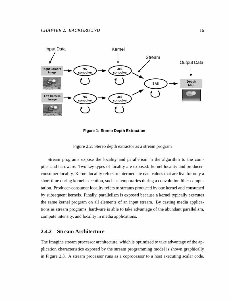
CHAPTER 2. BACKGROUND 16
Figure 1: Stereo Depth Extraction
Kernel
Stream
Input Data
Output Data
Left CameraImage
Right CameraImage
DepthMap
7x7convolve
7x7convolve
3x3convolve
3x3convolve
SAD
Figure 2.2: Stereo depth extractor as a stream program
Stream programs expose the locality and parallelism in the algorithm to the com-
piler and hardware. Two key types of locality are exposed: kernel locality and producer-
consumer locality. Kernel locality refers to intermediate data values that are live for only a
short time during kernel execution, such as temporaries during a convolution filter compu-
tation. Producer-consumer locality refers to streams produced by one kernel and consumed
by subsequent kernels. Finally, parallelism is exposed because a kernel typically executes
the same kernel program on all elements of an input stream. By casting media applica-
tions as stream programs, hardware is able to take advantage of the abundant parallelism,
compute intensity, and locality in media applications.
2.4.2 Stream Architecture
The Imagine stream processor architecture, which is optimized to take advantage of the ap-
plication characteristics exposed by the stream programming model is shown graphically
in Figure 2.3. A stream processor runs as a coprocessor to a host executing scalar code.

CHAPTER 2. BACKGROUND 17
Stream Processor
Microcontroller
ALU Cluster 7
ALU Cluster 6
ALU Cluster 5
ALU Cluster 4
ALU Cluster 3
ALU Cluster 2
ALU Cluster 1
ALU Cluster 0
StreamRegister File
StreamController
HostProcessor
StreamingMemorySystem
SDRAM
Figure 2.3: Stream Processor Block Diagram
Instructions sent to the stream processor from the host are sequenced through a stream con-
troller. The stream register file (SRF) is a large on-chip storage for streams. The microcon-
troller and ALU clusters execute kernels from a stream program. As shown in Figure 2.4,
each cluster consists of ALUs fed by two local register files (LRFs) each, external ports for
accessing the SRF, and an intracluster switch that connects the outputs of the ALUs and
external ports to the inputs of the LRFs. In addition, there is a scratchpad (SP) unit, used
for small indexed addressing operations within a cluster, and an intercluster communica-
tion (COMM) unit, used to exchange data between clusters. Imagine is a stream processor
recently designed at Stanford University that contains six floating-point ALUs per cluster
(three adders, two multipliers, and one divide-square-root unit) and eight clusters [Khailany
et al., 2001], and was fabricated in a CMOS technology with 0.18 micron metal spacing
rules and 0.15 micron drawn gate length.

CHAPTER 2. BACKGROUND 18
SP COMM
Intracluster SwitchTo/From
SRF
To/FromOther
Clusters
Figure 2.4: Arithmetic Cluster Block Diagram
Stream processors directly execute stream programs. Streams are loaded and stored
from off-chip memory into the SRF. SIMD execution of kernels occurs in the arithmetic
clusters. Although the stream processor in Figure 2.3 conatins eight arithmetic clusters,
in general, the stream processor architecture can contain an arbitrary number of arithmetic
clusters, represented by the variable C. For each iteration of a loop in a kernel, C clus-
ters will read C elements in parallel from an input stream residing in the SRF, perform
the exact same series of computations as specified by the kernel inner loop, and write C
output elements in parallel back to an output stream in the SRF. Kernels repeat this for
several loop iterations until all elements of the input stream have been read and operated
on. Data-dependent conditionals in kernels are handled with conditional streams which,
like predication, keep control flow in the kernel simple [Kapasi et al., 2000]. However,
conditional streams eliminate the extra computation required by predication by converting
data-dependent control flow decisions into data-routing decisions.
Stream processors exploit parallelism and locality at both the kernel level and applica-
tion level. During kernel execution, data-level parallelism is exploited with C clusters con-
currently operating on C elements and instruction-level parallelism is exploited by VLIW
execution within the clusters. At the application level, stream loads and stores can be over-
lapped with kernel execution, providing more concurrency. Kernel locality is exploited
by stream processors because all temporary values produced and consumed during a ker-
nel are stored in the cluster LRFs without accessing the SRF. At the application level,

CHAPTER 2. BACKGROUND 19
producer-consumer locality is exploited when streams are passed between subsequent ker-
nels through the SRF, without going back to external memory.
The data in media applications that exhibits kernel locality and producer-consumer
locality also has high data bandwidth requirements when compared to available off-chip
memory bandwidth. Stream processors are able to support these large bandwidth require-
ments because their register files provide a three-tiered data bandwidth hierarchy. The first
tier is the external memory system, optimized to take advantage of the predictable memory
access patterns found in streams [Rixner et al., 2000a]. The available bandwidth in this
stage of the hierarchy is limited by pin bandwidth and external DRAM bandwidth. Typi-
cally, during a stream program, external memory is only referenced for global data accesses
such as input/output data. Programs are strip-mined so that the processor reads only one
batch of the input dataset at a time. The second tier of the bandwidth hierarchy is the SRF,
which is used to transfer streams between kernels in a stream program. Its bandwidth is
limited by the available bandwidth of on-chip SRAMs. The third tier of the bandwidth
hierarchy is the cluster LRFs and the intracluster switch between the LRFs which forwards
intermediate data in a kernel between the ALUs in each cluster during kernel execution.
The available bandwidth in this tier of the hierarchy is limited by the number of ALUs one
can fit on a chip and the size of the intracluster switch between the ALUs.
The peak bandwidth rates of the three tiers of the data bandwidth hierarchy are matched
to the bandwidth demands in typical media applications. For example, the Imagine proces-
sor contains 40 fully-pipelined ALUs and provides 2.3 GB/s of external memory band-
width, 19.2 GB/s of SRF bandwidth, and 326.4 GB/s of LRF bandwidth. As discussed in
Section 2.1, some media applications such as the stereo depth extractor require over 400 in-
herent ALU operations per memory reference. Imagine supports a ratio of ALU operations
to memory words referenced of 28. Therefore, not only are stream processors in today’s
technology with tens of ALUs able to exploit this compute intensity, but as VLSI capac-
ity continues to scale at 70% annually and as memory bandwidth continues to increase at
25% annually, this suggests that stream processors with thousands of ALUs could provide
significant speedups on media applications without becoming memory bandwidth limited.

CHAPTER 2. BACKGROUND 20
2.4.3 Stream Processing Related Work
The stream processor architecture described above builds on previous work in data-parallel
architectures and programming models.
Stream processors share with vector processors the ability to exploit large amounts of
data paralellism and compute intensity, but they differ from vector processors in two key
ways. First, vector processors execute simple vector instructions such as vector adds and
multiplies on vectors located in the vector register file whereas stream processors execute
microcode kernels in SIMD out of the stream register file. Second, the register file storage
on a stream processor is split into the stream register file and local register files. These
optimizations allow stream processors to both capture producer-consumer locality in the
register file hierarchy and to provide improved scalability within the arithmetic clusters
with the local register files. Related work in vector processors has explored the use of
partitioned register files to improve their scalability [Kozyrakis and Patterson, 2003].
Although designing a programmable architecture to directly execute stream programs
is new, programming models similar to the stream model have been proposed in previous
work with fixed-function processors. One example of a fixed-function processor that di-
rectly executes the stream programming model is Cheops [Bove and Watlington, 1995].
It directly maps an application data-flow exposed by the stream programming model into
hardware units and consists of a set of specialized stream processors where each processor
accepts one or two data streams as input and produces one or two data streams as output.
Data streams are either forwarded directly from one stream processor to the next according
to the applications data-flow graph or transferred between memory and the stream proces-
sors.
Other researchers have proposed designing signal processing systems using signal flow
graphs specified in Simulink [Simulink, 2002] or other programming models [Lee and
Parks, 1995] that have many similarities with the stream programming model. With these
systems, signal flow graphs can be synthesized to software running on DSPs [Bhattacharyya
et al., 1996; de Kock et al., 2000] or can be mapped into fixed-function processors using
hardware generators [Davis et al., 2001]. Designing fixed-function processors with these
techniques allows for high efficiency since available parallelism and producer-consumer
CHAPTER 2. BACKGROUND 21
locality can easily be exploited. However, unlike programmable processors, fixed-function
processors lack the flexibility to execute a wide variety of applications.
Recently, other researchers have applied these same techniques for exploiting paral-
lelism and locality used in fixed-function processors to reconfigurable logic. Streams-
C [Gokhale et al., 2000] and others [Caspi et al., 2001] have proposed mapping arithmetic
kernels to blocks in FPGAs and mapping streams passed between kernels to FIFO-based
communication channels between FPGA blocks. These techniques enable some degree
of programmability with a high-level language and are able to exploit large amounts of
parallelism in stream programs. However, this approach is inhibited by limitations in re-
configurable logic. When compared to fixed-function transistors, large area and energy
overheads are incurred when a design is implemented in reconfigurable logic. Further-
more, since stream programs are being spatially mapped onto a fixed resource such as an
FPGA, problems arise when applications are too complex to fit onto this fixed resource.
Finally, other researchers have also studied compiling and executing the stream pro-
gramming model on chip multiprocessors. Streamit is a programming language that im-
plements the stream model on the RAW CMP [Gordon et al., 2002]. Like hardwired
stream processors, CMPs executing compiled stream programs can exploit parallelism
with threads and producer-consumer locality between processors to manage communica-
tion bandwidth effectively. Like CMPs, programmable stream processors also have the
ability to exploit parallelism and locality. However, since CMPs are targeted to run a wide
variety of applications and rely mostly on thread-level parallelism, they contain more gen-
eral control and communication structures per processor. In contrast, stream processors are
targeted specifically for media applications, and therefore can use data-parallel hardware
to efficiently exploit the available parallelism and a register file organization to efficiently
exploit the available locality.
2.4.4 VLSI Efficiency of Stream Processors
The bandwidth hierarchy provided by a stream architecture’s register file organization al-
lows stream processors to sustain a large percentage of peak performance with very modest
off-chip memory bandwidth requirements. However, the other advantage of the register

CHAPTER 2. BACKGROUND 22
file organization is the area and energy efficiency derived from partitioning the register file
storage into stream register files, arithmetic clusters, and local register files within the arith-
metic clusters. This partitioning enables stream processors to scale to thousands of ALUs
with significantly modest area and energy costs.
The area of a register file is the product of three terms: the number of registers R, the
bits per register, and the size of a register cell. Asymptotically, with a large number of ports,
each register cell has an area that grows with p2 because one wire is needed in the word-line
direction, and another wire needed in the bit-line direction per register file port. Register
file energy per access follows similar trends. Therefore, a highly multi-ported register
file has area and power that grows asymptotically with Rp2 [Rixner et al., 2000b]. A
general-purpose processor containing N arithmetic units with a single centralized register
file requires approximately 3N ports (two read ports for the operands and one wire port
for the result per ALU). However, as N increases, working set sizes would also increase,
meaning that R should also grow linearly with N . As a result, a single centralized multi-
ported register file interconnecting N arithmetic units in a general-purpose microprocessor
has area and power that grows with N3, and would quickly begin to dominate processor
area and power. As a result, partitioning register files is necessary in order to efficiently
scale to large numbers of arithmetic units per processor.
Historically, register file partitioning has been used extensively in programmable pro-
cessors in order to improve scalability, area and energy efficiency, and to reduce wire delay
effects. For example, the TI C6x [Agarwala et al., 2002] is a VLIW architecture split
into two partitions, each containing a single multi-ported register file connected to four
arithmetic units. Even in high-performance microprocessors not necessarily targeted for
energy efficient operation, such as the Alpha 21264 [Gieseke et al., 1997], register file par-
titioning has been used. In the stream architecture, register file partitioning occurs along
three dimensions: distributed register files within the clusters, SIMD register files across
the clusters, and the stream register organization between the clusters and memory. In the
remainder of this section, we explain how the register file partition of Imagine along these
three dimensions improves area and energy efficiency and is related to previous work on
partitioned register files.

CHAPTER 2. BACKGROUND 23
Distributed Register Partitioning
The first register file partitioning in the stream architecture is along the ILP dimension
within a cluster. Given N ALUs per cluster, a VLIW cluster with one centralized register
file connected to all of the ALUs would grow with N3 as explained above. However,
by splitting this centralized multi-ported register file into an organization with one two-
ported LRF per ALU input within each arithmetic cluster, the area and power of the LRFs
only grows with N , and the intracluster switch connecting the ALU outputs to the LRF
inputs grows with N2 asymptotically. The exact area efficiency, energy efficiency, and
performance when scaling N on a stream architecture will be explored in more detail in
Chapter 6.
The disadvantage of this approach is that the VLIW compiler must explicitly manage
communications across this switch and must deal with replication of data across various
LRFs [Mattson et al., 2000]. However, using asymptotic models for area and energy of
register files, Rixner et al. showed that for N = 8, this distributed register organization
provides a 6.7x and an 8.7x reduction on area and energy efficiency respectively in the
ALUs, register files, and switches2 [Rixner et al., 2000b].
Partitioned register files in VLIW processors and explicitly scheduled communications
between these partitions were proposed on a number of previous processors. For example,
the TI C6x [Agarwala et al., 2002] contains two partitions with four arithmetic units per
partition. In addition, a number of earlier architectures used partitioned register files of
various granularities. The Polycyclic architecture [Rau et al., 1982], the Cydra [Rau et
al., 1989], and Transport-triggered architectures [Janssen and Corporaal, 1995] all had
distributed register file organizations.
SIMD Register Partitioning
Whereas the distributed register partitioning was along the ILP dimension and was handled
by the VLIW compiler, the next partitioning in the stream architecture occurs in the DLP
2Implementation details such as design methodology or available wiring layers would affect the efficiencyadvantage of certain DRF organizations. For instance, comparing the efficiency of one four-ported LRFper ALU rather to one two-ported LRF per ALU input would provide different results depending on theseimplementation details.

CHAPTER 2. BACKGROUND 24
dimension and corresponds to the SIMD arithmetic clusters. In an architecture with C
SIMD clusters, each of these clusters requires interconnecting only N/C ALUs together.
Therefore, the area and energy in each cluster’s intracluster switch grows much more slowly
as there are many fewer ALUs per cycle. The disadvantage is that the complexity of the
intercluster switch grows as the number of clusters increases. This tradeoff will be explored
in more detail in Chapter 6.
The other efficiency advantage of SIMD processing besides register file partitioning
comes from amortizing control overhead. Only one instruction fetch unit and sequencer is
required for C clusters. The area and efficiency gains achieved through SIMD-partitioned
register files and by amortizing control over parallel vector lanes were first proposed on
vector microprocessors, and are applied to the stream architecture register file organization
as well. Furthermore, SIMD partitioning can be combined with distributed register par-
titioning, as demonstrated both in the Imagine stream processor and in the CODE vector
microarchitecture [Kozyrakis and Patterson, 2003].
Separating the SRF storage from cluster storage
The third and final partition in the stream architecture register file is a split between stor-
age for loads and stores and storage for intermediate buffering between individual ALU
operations. This is accomplished by separating the SRF storage from the LRFs within each
cluster. This splitting between the SRF and LRFs has two main advantages. First, stag-
ing data for loads and stores is capacity-limited because of long memory latencies, rather
than bandwidth-limited, meaning that large memories with few ports can be used for the
SRF whereas the capacity of the LRFs can be kept relatively small. Second, data can be
staged in the SRF as streams, meaning that accesses to the SRF will be sequential and pre-
dictable. As a result, streambuffers can be used to prefetch data into and out of the SRF,
much like streambuffers are often used to prefetch data from main memory in micropro-
cessors [Jouppi, 1990]. As explained in Section 3.2.4, these streambuffers allow accesses
to a stream from each SRF client to be aggregated into larger portions of a stream before
they are read or written from the SRF, leading to a much more efficient use of the SRF
bandwidth and a more area- and energy-efficient design.

CHAPTER 2. BACKGROUND 25
VLSI Efficiency Summary
The stream architecture register file organization can be viewed as a combination of the
above three register partitionings. Overall, these partitions each provide a large benefit in
area and energy efficiency. When compared to a 48-ALU processor with a single unified
register file, a C = 8 N = 6 stream processor takes 195 times less area and 430 times
less energy. A performance degradation of 8% over a hypothetical centralized register
file architecture is incurred due to SIMD instruction overheads and explicit data transfers
between partitions [Rixner et al., 2000b].
In summary, there is a large and growing gap between the area and energy efficiency
of special-purpose and programmable processors on media applications. The stream ar-
chitecture attempts to bridge that gap through its ability to exploit important application
characteristics and its efficient register file organization.

Chapter 3
Imagine: Microarchitecture and Circuits
In the previous chapter, a stream processor architecture [Rixner et al., 1998; Rixner, 2001]
was introduced to bridge the efficiency gap between special-purpose an programmable pro-
cessors. A stream processor’s efficiency is derived from several architectural advantages
over other programmable processors. The first advantage is a data bandwidth hierarchy
for effectively dealing with limited external memory bandwidth that can also exploit com-
pute intensity and producer-consumer locality in media applications. The next advantage
is SIMD arithmetic clusters and multiple arithmetic units per cluster that can exploit both
DLP and ILP in media processing kernels. Finally, the bandwidth hierarchy and SIMD
arithmetic clusters are built around a area- and energy-efficient register file organization.
Although the previous analysis qualitatively demonstrates the efficiency of the stream
architecture, in order to truly evaluate its performance efficiency, a VLSI prototype Imag-
ine stream processor [Khailany et al., 2001] was developed so that performance, power
dissipation, and area could be measured. Not only did this prototype provide a vehicle for
experimental measurements, but also, by implementing a stream processor in VLSI, key
insights into the effect of technology on the microarchitecture are gained. These insights
were then used to study the scalability of stream processors in Chapter 6 and Chapter 7.
The next few chapters discuss the Imagine prototype in detail. This chapter presents
the instruction set architecture, microarchitecture, and circuits of key components from the
Imagine stream processor. Chapter 5 discusses the design methodology used for Imagine,
and finally, in Chapter 6, experimental results for Imagine are presented.
26

CHAPTER 3. IMAGINE: MICROARCHITECTURE AND CIRCUITS 27
3.1 Instruction Set Architecture
The Imagine processor runs stream programs written in KernelC and StreamC. StreamC
specifies how streams are passed between kernels and includes reads and writes from mem-
ory and I/O. KernelC contains the mathematical operations for the kernels. Software tools
then compile StreamC and KernelC for execution into instructions from the stream-level
and kernel-level instruction set architectures (ISAs). StreamC compilation involves high-
level data-flow analysis at the stream level including SRF allocation and memory man-
agement [Mattson, 2001; Kapasi et al., 2001]. KernelC compilation includes parsing, in-
struction scheduling, and managing the communication between ALUs and LRFs across
the intracluster switch [Mattson et al., 2000]. Once StreamC and KernelC have been com-
piled, the Imagine processor directly executes instructions from the stream and kernel level
ISAs described below.
3.1.1 Stream-Level ISA
There are six main stream-level instructions:
• LOAD transfers streams from off-chip SDRAM to the SRF.
• STORE transfers streams from the SRF to off-chip DRAM.
• RECEIVE transfers streams from the network to the SRF.
• SEND transfers streams from the SRF to the network.
• CLUSTER OP executes a kernel in the arithmetic clusters that reads inputs streams
from the SRF, computes output streams, and writes the output streams to the SRF.
• LOAD MICROCODE loads streams consisting of kernel microcode (576-bit VLIW
instructions) from the SRF into the microcontroller instruction store (a total of 2,048
instructions).
In addition to the six main instructions listed above, there are other instructions for
writes and reads to on-chip control registers which are inserted as needed by the stream-
level compiler. Streams must have lengths that are a multiple of eight (the number of

CHAPTER 3. IMAGINE: MICROARCHITECTURE AND CIRCUITS 28
MUL MUL DSQ SP COM
Intracluster SwitchIO Ports(To SRF)
To/FromOther
ClustersADD ADD ADD JB/VAL
Figure 3.1: Imagine Arithmetic Cluster
clusters) and lengths from 0 to 8K words are supported, where each word is 32 bits. Stream
instructions are fetched and dispatched by a host processor to a scoreboard in the on-chip
stream controller. As will be described in Section 3.2.8, the stream controller issues stream
instructions to the various on-chip units as their dependencies become satisfied and their
resources become available.
3.1.2 Kernel-Level ISA
Kernel-level instructions are scheduled and assembled into VLIW instructions at compile-
time, are sequenced by a microcontroller, and then are broadcast to and executed in eight
SIMD arithmetic clusters. Each arithmetic cluster, detailed in Figure 3.1, contains eight
functional units (plus the special JB and VAL units that are used for conditional streams [Ka-
pasi et al., 2000]). A small two-ported local register file (LRF) connects to each input of
each functional unit. An intracluster switch connects the outputs of the functional units to
the inputs of the LRFs.
Each function unit from Figure 3.1 executes instructions from the kernel-level instruc-
tion set, shown in Tables 3.1 and 3.2. Instructions are grouped by supported datatypes.
A wide range of datatypes from fixed-point or integer to single-precision floating-point
are supported in order to accommodate the demands of media applications. The first two
columns in the Kernel ISA tables contain the instruction mnemonic and a brief summary
of the operation performed. The third column specifies the latency of each operation and
the fourth column specifies the supported functional unit(s). As will be explained in Sec-
tion 3.2, all functional units except the DSQ unit are fully pipelined.
In addition to the function unit operations and the stream input/output instructions,

CHAPTER 3. IMAGINE: MICROARCHITECTURE AND CIRCUITS 29
Table 3.1: Kernel ISA - Part 1Op Description T Unit
Ops for Floating-Point Data-typesFADD Add 4 ADDFSUB Subtract 4 ADDFABS Absolute value 1 ADDFLT Test < 2 ADDFLE Test ≤ 2 ADDFTOI Convert to int (round-to-zero) 3 ADDFFRAC Computes x-FTOI(x) 4 ADDITOF Convert int to floating-point 4 ADDFMUL Multiply 4 MULFDIV Divide 17 DSQFSQRT Square root 16 DSQOps for 32b, 16b, and 8b DatatypesIADD Add 2 ADDISUB Subtract 2 ADDIABD/UABD Absolute difference (integer/unsigned) 2 ADDILT/ULT Test < (integer/unsigned) 2 ADDILE/ULE Test ≤ (integer/unsigned) 2 ADDIEQ Test == 1 ADDNEQ Test ! = 1 ADDAND Bitwise AND 1 ADDOR Bitwise OR 1 ADDXOR Bitwise XOR 1 ADDNOT Bitwise invert 1 ADDOps for 32b and 16b DatatypesIADDS/UADDS Integer/Unsigned saturating add 2 ADDISUBS/USUBS Integer/Unsigned saturating subtract 2 ADDSHIFT Logical shift 1 ADDSHIFTA Arithmetic shift 1 ADDROTATE Rotate 1 ADDIMUL/UMUL Integer/Unsigned multiply 4 MULIMULR/UMULR Integer/Unsigned multiply & round 4 MULOps for 16b DatatypesIMULD/UMULD Integer/Unsigned multiply (32b outputs) 4 MULOps for 32b DatatypesIDIV/UDIV Integer/Unsigned divide 22 DSQIDIVR/UDIVR Integer/Unsigned remainder 23* DSQ

CHAPTER 3. IMAGINE: MICROARCHITECTURE AND CIRCUITS 30
Table 3.2: Kernel ISA - Part 2Op Description T Unit
Data Movement OpsSELECT Multiplex based on cc 1 ALLNSELECT Multiplex based on !cc 1 ALLCCTOI Convert CC to int 1 ALLSHUFFLE Shuffle bytes 1 ADDSHUFFLED Shuffle bytes (two outputs) 1 MULSPRD Scratchpad read 2 SPSPWR Scratchpad write 2 SPCOMM Cluster RF - controlled permute 1 COMCOMMUCDATA Same as comm w/ UC data input 1 COMCOMMUCPERM UC-controlled permute 1 COMConditional Stream OpsINIT CISTATE Initialize JBRF entry for conditional input stream 1 JBINIT COSTATE Initialize JBRF entry for conditional output stream 1 JBGEN CISTATE Update JBRF entry with new state 1 JBGEN COSTATE Update JBRF entry with new state 1 JBGEN COSTATE Update JBRF entry with new state 1 JBSPCRD Conditional scratchpad read 2 SPSPCWR Conditional scratchpad write 2 SPINIT VALID Initialize valid unit for new conditional stream 1 VALGEN CCEND Computes CC for end of conditional stream 1 VALGEN CCFLUSH Computes CC for end of conditional stream 1 VALStream Input/Output OpsDATA IN Read from input stream 1 IOCOND IN R Conditional stream read - intermediate word in record 3 IOCOND IN D Conditional stream read - last word in record 3 IODATA OUT Write to output stream 1 IOCOND OUT R Conditional stream write - intermediate word in record 1 IOCOND OUT D Conditional stream write - last word in record 1 IOMicrocontroller OpsLOOP Branch to new PC (if last CHK was true) 3 UCNLOOP Branch to new PC (if last CHK was false) 3 UCUC DATA IN Load immediate into microcontroller RF 1 UCDEC CHK UCR Decrement and zero-check microcontroller RF value 2 UCCHK EOS Check for end of stream 2 UCCHK ANY Check for true cc in any cluster 2 UCCHK ALL Check for true cc’s in all clusters 2 UCSYNCH Synchronize with stream controller 1 UC
CHAPTER 3. IMAGINE: MICROARCHITECTURE AND CIRCUITS 31
the kernel-level instructions also control register file accesses and the intracluster switch.
Register file reads are handled with an address field in the kernel-level ISA, while writes
require both an address field and a software pipeline stage field. Finally, the kernel-level
ISA controls the intracluster switch with a bus select field for each write port. This field
specifies which function unit output or input port should be written into the register file for
this instruction.
3.1.3 Kernel Instruction Format
Once KernelC is mapped into instructions from the kernel-level ISA and scheduled by
the VLIW compiler, instructions are then assembled into the 576-bit format specified in
Figure 3.2. There are fields for nine functional units (scratchpad, ALUs, MULs, DSQ,
COMM, and JBVAL), the condition code register file (CC), explained in Section 3.2, as
well as the microcontroller and eight stream input/output units (SB0:SB7). Each function
unit field is further subdivided into sub-fields, containing an opcode, a CCRF read address,
read addresses for both LRFs (LRF 0 Rd and LRF 1 Rd), write addresses for both LRFs
(LRF 0 Wr and LRF 1 Wr), a software pipelining stage field associated with each LRF write
port (LRF 0 Stg and LRF 1 Stg), and a bus select field for the LRF inputs that controls the
intracluster switch (LRF 0 Bus and LRF 1 Bus).
The location of function unit fields within the instruction word corresponds roughly to
floorplan placement of arithmetic units within an arithmetic cluster. This alignment reduces
the length of control wires as instructions are fetched from the microcode store, decoded,
and broadcast to the clusters.
3.2 Microarchitecture
In the previous chapter, the arhitecture of the Imagine stream processor, shown in Fig-
ure 2.3, and the basic execution of a stream processor was presented. In this section,
this discussion is extended with microarchitectural details from the key components of
the Imagine architecture. First, the microarchitecture and pipeline diagrams of the micro-
controller and arithmetic clusters are presented. These units execute instructions from the

CHAPTER 3. IMAGINE: MICROARCHITECTURE AND CIRCUITS 32
Scratchpad
Res
075
DSQ
76112
ALU2
113152
MUL1
153195
MUL0
196238
CC
239254
ALU1
255294
ALU0
295334
COMM
335371
JB/VAL
372413
Microcontroller
414488
SB0:SB7
489568576
Opcode
Function Unit Sub-Fields
CCRF
Rd
LRF1
Rd
LRF1
Stg.
LRF0
Rd
061014182125293336
LRF1
Wr
LRF1
Bus
LRF0
Wr
LRF0
Stg.
LRF0
Bus
Figure 3.2: VLIW Instruction Format
kernel-level ISA. Next, both the stream register file microarchitecture and its pipeline di-
agram are described. Finally, we present the stream controller and the streaming memory
system, the other major components of a stream processor.
3.2.1 Microcontroller
The microcontroller provides storage for the kernels’ VLIW instructions, and sequences
and issues these instructions to the arithmetic clusters during kernel execution. A block di-
agram of the Imagine microcontroller is shown in Figure 3.3. It is composed of nine banks
of microcode storage as well as blocks for loading the microcode, sequencing instructions
using a program counter, and instruction decode.
Each bank of microcode storage contains a single-ported SRAM where 64 bits of each
576-bit VLIW kernel instruction are stored. Since each bank contains a 128Kb SRAM, a
total of 2K instructions can be stored at one time. In order to allow for microcode to be
loaded during kernel execution without a performance penalty, two instructions are read
at one time from the SRAM array. The first of these instructions is passed directly to the

CHAPTER 3. IMAGINE: MICROARCHITECTURE AND CIRCUITS 33
1024 x 128bSRAM
Microcode StoreBank 8
1024 x 128bSRAM
Microcode StoreBank 0
MicrocodeLoader
FromSRF
Din A Din A
Kernel Instruction[575:512]
InstructionSequencer
Kernel Instruction[63:0]
Instruction Decoder
To Microcontroller, SRF, Arithmetic Clusters
From StreamController
Dout Dout
UCRF
Figure 3.3: Microcontroller Block Diagram
instruction decoder. The second is stored in a register, so that it can be decoded in the next
clock cycle without accessing the SRAM array again.
The microcode loader handles the loading of kernel instructions from the SRF to the
microcode storage arrays. Since microcode is read from the SRF one word at a time,
and 1152 bits of microcode must be written at a time, the microcode loader reads words
from a stream in the SRF, then sends them to local buffers in one of the microcode store
banks. Once these buffers have all been filled, the microcode loader requests access to write
two instructions into the microcode storage banks. A controller, not shown in Figure 3.3,
handles this arbitration and also controls the reading of instructions from the microcode
storage and intermediate registers during kernel execution.
The instruction sequencer contains the program counter which is used to compute the
addresses to be read from the microcode storage. At kernel startup, the program counter

CHAPTER 3. IMAGINE: MICROARCHITECTURE AND CIRCUITS 34
is loaded with the address of the first kernel instruction, specified by the stream controller.
As kernel execution proceeds, the program counter is either incremented or, on condi-
tional branch instructions, a new address is computed and loaded into the program counter.
Conditional branches are handled with the CHK and LOOP/NLOOP instructions. CHK
instructions store a true or false value into a register inside the instruction sequencer. Based
on the value of this register, LOOP instructions conditionally branch to a relative offset
specified in the instruction field.
The final component of the microcontroller is the instruction decoder, which handles
the squashing of register file writes, a key part of the software pipeline mechanism on
Imagine. In the VLIW instruction, each register file write has a corresponding stage field,
which allows the kernel scheduler to easily implement software pipeline priming and drain-
ing without a loop pre-amble and post-amble. The kernel scheduler assigns all register file
writes to a software pipelining stage, and encodes this stage in the VLIW instruction as
the LRF Stg. sub-field from Figure 3.2. During loops, the instruction decoder keeps track
of which stages are currently active, and squashes register file writes from inactive stages.
In addition to squashing register file writes, the instruction decoder also provides pipeline
registers and buffers for each ALU and LRF’s opcodes before they are distributed to the
SIMD ALU clusters and the instruction decoder handles reads and writes from the micro-
controller register file, which is used to store constants and cluster permutations in many
kernels.
3.2.2 Arithmetic Clusters
As the microcontroller fetches and sequences VLIW instructions from the microcode stor-
age, the eight SIMD arithmetic clusters on Imagine execute these instructions. As was
shown in Figure 3.1, each cluster is composed of nine function units (3 ADDs, 2 MULs,
1 DSQ, 1 SP, 1 JB/VAL, 1 COM). A more detailed view of a function unit (FU) and its
associated register files is shown in Figure 3.4.
Most FUs have two data inputs, one condition code (cc) input, and one output bus.
Data in the arithmetic clusters is stored in the LRFs. The LRFs have one read port, one
write port, and 16 entries each, except for the multiplier LRFs, which have 32 entries.

CHAPTER 3. IMAGINE: MICROARCHITECTURE AND CIRCUITS 35
FU Result Bus
FunctionUnit
LRFs
FU ResultBuses
FU ResultBuses
CC ResultBuses
LocalCopy
ofCCRF
Figure 3.4: Function Unit Details
D
EN
Q
LRF Bitslice
D
EN
Q2-level
4:1MuxTree
LRF Input [0](from FU result
bus mux) LRF Output [0](To FU)
D
EN
Q
LRF Bitslice
D
EN
Q2-level
4:1MuxTree
LRF Input [31](from FU result
bus mux) LRF Output [31](To FU)
WriteSelect[1]
WriteSelect[15]
Figure 3.5: Local Register File Implementation

CHAPTER 3. IMAGINE: MICROARCHITECTURE AND CIRCUITS 36
Latches were used as the basic storage element for the LRFs, as shown in Figure 3.5. The
multiplexer before the LRF output flip flop enables register file bypassing within the LRFs
so that data written on one cycle can be read correctly by the FU in the subsequent cycle.
Flip flop writes can be disabled by selecting the top feedback path through the multiplexer.
Each FU also contains a copy of the condition code register file (CCRF), not shown
in Figure 3.1, but shown in the detailed view of Figure 3.4. Condition codes (CCs) are
special data values generated by comparison instructions such as IEQ and FLT and are
used with SELECT instructions and with conditional streams. Although there is only one
CCRF in the ISA, each FU contains a local copy of the CCRF. During writes to the CCRF,
data and write addresses are broadcast to each CCRF copy, whereas during reads, each FU
reads locally from its own CCRF copy. This structure allows for a CCRF with as many
read ports as there are FUs, yet does not incur any wire delay when accessing CCs shared
between all of the FUs in a cluster.
Finally, data is exchanged between FUs via the intracluster switch. This switch is
implemented as a full crossbar where each FU broadcasts its result bus(es) to every LRF
in an arithmetic cluster. A multiplexer uses the bus select field for its associated LRF write
port to select the correct FU result bus for the LRF write.
3.2.3 Kernel Execution Pipeline
The microcontroller and arithmetic clusters work together to execute kernels. As is typi-
cally done in most high-performance microprocessors, they operate in a pipelined manner
in order to achieve higher instruction throughput. The kernel execution pipeline diagram in
the microcontroller and arithmetic clusters is shown in Figure 3.6.
During the first two pipeline stages, FETCH1 and FETCH2, the microcontroller in-
struction sequencer sends the current program counter to the microcode storage banks and
the VLIW instructions are fetched from the SRAMs. During the decode and distribute stage
(DECODE/DIST), instructions are decoded and broadcast to the eight arithmetic clusters.
Branches are resolved and branch targets are computed in this stage, and the new program
counter is computed if necessary. Since this is the third pipeline stage, two branch delay
slots are added to all LOOP instructions. During REG READ, more instruction decoding

CHAPTER 3. IMAGINE: MICROARCHITECTURE AND CIRCUITS 37
FETCH1 FETCH2 DECODE/DIST
REGREAD EX 1 EX N WB
FETCH1 FETCH2DECODE/
DISTREG
READ EX 1 EX N WB
FETCH1 FETCH2DECODE/
DISTREG
READ EX 1 EX N WB
Cycle 1 Cycle 2 Cycle 3 Cycle 4 Cycle 5
Figure 3.6: Kernel Execution Pipeline Diagram
occurs and LRFs are accessed locally in each arithmetic cluster. This is followed by the
execute (EX) pipeline stages, which vary in length depending on the operation being exe-
cuted. The last half-cycle of each function unit’s last execute stage is used to traverse the
intracluster switch, and then in the writeback (WB) stage, the register write occurs.
Although the clusters are statically scheduled by a VLIW compiler and sequenced by
a single microcontroller, dynamic events during execution can cause the kernel execution
pipeline to stall. Stalls are caused by one of three conditions: the SRF not being ready for
a write to an output stream, the SRF not being ready for a read from an input stream, or
a SYCNH instruction being executed by the microcontroller for synchronization with the
host processor. When one of these stall conditions is encountered, all pipeline registers in
the clusters and microcontroller are disabled and writes to machine state are squashed until
a later cycle when the stall condition is no longer valid.
The microcontroller and arithmetic clusters work together to execute kernels from an
application’s stream program. They execute VLIW instructions made up of operations
from the kernel-level ISA in a six-stage (or more for some operations) execution pipeline.
The other main blocks in the Imagine processor are used to sequence and execute stream
transfers from the stream-level ISA.

CHAPTER 3. IMAGINE: MICROARCHITECTURE AND CIRCUITS 38
SB 0Bank 0
(8 words)
SRFBank 0
(4K words)4
words
SB 0Bank 7
(8 words)
22SBs
SRFBank 7
(4K words)
SRFControl
22:1Arbiter
SB 0Control
SRAM Requests / Grants
Data to/from client 0
Control to/from client 0
SB 21Bank 0
(8 words)
SB 21Bank 7
(8 words)
SB 21Control
Data to/from client 21
Control to/from client 21
4words
Figure 3.7: Stream Register File Block Diagram

CHAPTER 3. IMAGINE: MICROARCHITECTURE AND CIRCUITS 39
3.2.4 Stream Register File
The stream register file (SRF), provides on-chip data storage for streams. The SRF is used
during execution to stage data both between stream-level memory and kernel operations
and between subsequent kernel operations. As shown in Figure 3.7, the SRF is partitioned
into eight parallel banks, where each bank is aligned to an associated cluster. Streams are
stored in the SRF with their records strided across the eight banks: bank 0 would contain
records 0, 8, 16, . . . , bank 1 would contain records 1, 9, 17, . . . , and so on for banks 2
through 8. Each SRF bank can store up to 4K words, for a total of 32K words.
Each SRF bank contains a single-ported 128kb SRAM and 22 streambuffer (SB) banks.
The SBs are used to interface between the SRF storage and the 22 SRF clients (8 cluster,
8 network, 1 microcontroller, 1 host, 2 memory data, and 2 memory index streams)1. Us-
ing streambuffers as these clients’ interface to the SRF takes advantage of the predictable
streaming nature of accesses to enable an area- and energy-efficient SRF implementa-
tion [Rixner et al., 2000b]. Clients make requests to the streambuffers to read or write
elements from a stream. SBs in turn make requests to access the location in the SRF stor-
age where that stream resides. These requests are handled by a 22:1 arbiter in SRF control.
One SB is granted access per cycle and all eight banks from the chosen SB read or write
4 words into half of their local storage (each SB contains 8 words of storage to allow for
double buffering). Finally, the external clients can read or write data from their associ-
ated streambuffer at a lower bandwidth. In this manner, the SBs enable the SRAM’s single
physical port to function as 22 logical ports, but in a more area- and energy-efficient manner
than a multi-ported SRAM.
3.2.5 SRF Pipeline
Not only is kernel execution pipelined in order to provide higher instruction throughput,
but the SRF is also pipelined to provide high-throughput access to the SRF storage. The
pipeline diagram for the SRF is shown in Figure 3.8, and is designed to operate at half the
1Each client accesses its streambuffers in a slightly different manner. The clusters read or write 8 wordsfrom each streambuffer in parallel from each cluster for a peak supported throughput of 8 words per cycle perstreambuffer. Although the network has 8 SBs, only 2 can be active on a given cycle, and only 2 words perSB can be read. All of the other streambuffers support 1 word per cycle.

CHAPTER 3. IMAGINE: MICROARCHITECTURE AND CIRCUITS 40
SEL MEM WB
SEL MEM WB
SEL MEM WB
Cycle 1 Cycle 2 Cycle 3 Cycle 4 Cycle 5
Figure 3.8: SRF Pipeline Diagram
frequency of the kernel pipeline, in order to ease timing constraints, and therefore reduce
overall design effort.
The SRF pipeline consists of three stages: stream select (SEL), memory access (MEM),
and streambuffer writeback (WB). During the SEL stage, SBs arbitrate for access to the
SRAM array, and one of the SBs is granted access. Meanwhile the arbiter state is updated
using a last-used-last-served scheme to ensure fairness among SB access. During the MEM
stage, the SB that was granted access transfers data between its local storage and the SRAM
array. Finally, during the WB stage, which only occurs on SRF reads, data from the SRAM
array is written locally to the eight SB banks. While the SRF storage and control operates
at half speed, the SBs operate at full speed, so the WB stage only takes one additional clock
cycle to complete.
3.2.6 Streaming Memory System
The streaming memory system executes stream load and store instructions from the stream-
level ISA and supports up to two simultaneous instructions. The memory system is com-
posed of two address generators (one for each instruction being executed), four memory
banks, each with their own external DRAM interface (memory addresses are interleaved
among the four banks), and a reordering streambuffer in the SRF. Rixner provides details

CHAPTER 3. IMAGINE: MICROARCHITECTURE AND CIRCUITS 41
on the memory bank and address generator microarchitecture [Rixner, 2001].
Four types of accesses are supported by the streaming memory system: sequential,
strided, indexed, and bit-reversed. The address generators issue at most one word per cycle
of memory read or write requests based on these access patterns to the appropriate memory
banks. Within the memory banks, accesses are buffered, scheduled, and reordered by a
memory controller in order to maximize utilization of the off-chip DRAM [Rixner et al.,
2000a]. While the latency of individual memory accesses could increase by this reorder-
ing, the overall latency of the stream load or store is reduced since memory bandwidth is
improved with this technique. Since memory accesses are issued to the DRAM out of or-
der, stream elements read during loads are reordered when they are written back into the
streambuffer within the SRF to ensure proper ordering later during kernel execution.
3.2.7 Network Interface
The network interface on Imagine is used to connect the SRF to other Imagine chips in
multiprocessor systems or to read or write from I/O devices. Stream send or receive in-
structions are used to transfer streams across the network using source routing. Four exter-
nal network input channels and four output channels are supported. Each channel is able
to transfer 2 bytes each clock cycle, for a total network bandwidth of 2 input words and 2
output words per cycle per node. This is matched to the total bandwidth supported by the
network streambuffers.
Destinations and routes are written from the host processor into an entry in the Network
Routing Register File. Since source routing is used, arbitrary network topologies with up to
four physical channels per node are supported. One example of a supported topology would
be a two-dimensional mesh network. Streams sent across the network are packaged into
64-bit flits and virtual channel flow control is used to manage communication across the
network [Dally, 1992]. When the network interface receives a header flit into its ejection
queue, it signals the stream controller to start an SRF transfer. As data flits are received,
they are written two words at a time into one of the eight network streambuffers. A tail
flit signals the end of the stream causing all remaining data flits in the streambuffer to
be written to the SRF storage. Sending network streams work in a similar manner but in

CHAPTER 3. IMAGINE: MICROARCHITECTURE AND CIRCUITS 42
Issue andDecodeLogic
To Microcontroller,SRF,
Memory System,Network Interface
From HostProcessor SCTRF
Scoreboard
(32 entries)
Op Buffer
(32 instrs)
(Stream Ops)
(Dependencies)
ResourceAnalyzer
Status bits fromMicrocontroller,
SRF,Memory System,Network Interface
Arbiter Register transfers withmicrocontroller, SRF
Figure 3.9: Stream Controller Block Diagram
reverse with data being read from the streambuffers and packaged into flits as they are sent
into the network interface injection queue.
3.2.8 Stream Controller
The above blocks from the Imagine processor execute instructions from the stream-level
ISA. These instructions are issued by the host processor during the execution of stream pro-
grams. However, since the execution time of stream instructions is dynamically dependent
on stream lengths, memory access patterns, and kernel code, dynamic scheduling of stream
instructions is important in order to provide high utilization in both the memory system
and arithmetic clusters. The stream controller handles this dynamic scheduling of stream
instructions.
A block diagram of the stream controller is shown in Figure 3.9. Stream instructions
sent by the host processor are written into one of the 32 entries in the operation buffer.
Along with the instruction, the host processor sends bitmasks that specify dependencies
between this instruction and the other 32 instructions currently in the operation buffer.
This information is separated from the actual operation and is stored in the scoreboard.
Meanwhile, a resource analyzer monitors status bits from the execution units and sends
this information to the scoreboard as well. When a stream instruction’s required resources

CHAPTER 3. IMAGINE: MICROARCHITECTURE AND CIRCUITS 43
are free and its dependencies have been satisfied, it makes a request to an arbiter to be
issued this cycle. One instruction is granted access and is sent from the operation buffer to
the issue and decode logic. The issue and decode logic converts the instruction into control
information that start the stream instruction in the individual execution units. A stream
controller register file (SCTRF) is used to transfer scalar data such as stream lengths and
scalar outputs from kernels if necessary. Once the stream instruction execution completes,
its scoreboard entry is freed and subsequent instructions dependent on it can be issued.
By using dynamic scheduling of stream instructions, the stream controller ensures that
stream execution units can stay highly utilized. This allows Imagine to exploit task-level
parallelism by efficiently overlapping memory operations and kernel operations. Further-
more, the 32-entry operation buffer also allows the host processor to work ahead of the
stream processor since the host can issue up to 32 stream instructions until it is forced to
stall waiting for more scoreboard entries to be free. This buffering mitigates any effect the
latency of sending stream instructions to the stream processor would have on performance.
3.3 Arithmetic Cluster Function Units
In this section, the design of the arithmetic cluster function units will be discussed. These
function units execute the kernel-level instruction set from Table 3.1 and Table 3.2 and were
developed with a number of design goals in mind, including low area, high throughput, low
design complexity, low power, and low operation latency.
3.3.1 ALU Unit
Each cluster contains three ALU units that execute the addition, shift, and logical instruc-
tions listed in Table 3.1. Many of these instructions include support for floating-point,
32-bit integer, dual 16-bit, and quad 8-bit instructions. A block diagram of the ALU is
shown in Figure 3.10. It is divided into three major functional sub-blocks, corresponding
to pipeline stages in the execution of four-cycle operations. The ALU X1 sub-block ex-
ecutes integer shifts, logical operations, and the alignment shift portion of floating-point

CHAPTER 3. IMAGINE: MICROARCHITECTURE AND CIRCUITS 44
additions. The ALU X23 sub-block contains two pipeline stages and implements inte-
ger additions and the addition portion of floating-point adds. Rounding also occurs in the
ALU X23 stage during floating-point adds. Finally, the ALU X4 sub-block executes a
normalizing shift operation.
Operations requiring floating-point additions, such as FADD, FSUB, and others, are 4-
cycle operations and therefore use all three major sub-blocks. The ALU supports floating-
point arithmetic adhering to the IEEE 754 standard, although only the round-to-nearest-
even rounding mode and limited support for denormals and NaNs are supported [Coonen,
1980]. Additions supporting this standard can be implemented with an alignment shifter,
a carry-select adder for summing the mantissas and doing the rounding, and a normalizing
shifter [Goldberg, 2002; Kohn and Fu, 1989]. This basic architecture was used in the ALU
unit.
Floating-point operands are comprised of a sign bit, eight bits for an exponent, and
23 bits for a fraction with an implied leading one. In the ALU X1 block, a logarithmic
shifter [Weste and Eshraghian, 1993] is used to shift the operand with the smaller exponent
to the right by the difference between the two exponents. If the sign bits of the two operands
are different, then the shifted result is also bitwise inverted, so that subtraction rather than
addition will be computed in the ALU X23 stage. Furthermore, both the unshifted and
shifted fractions are then shifted to the left by two bits such that the leading one of the
unshifted operand is at bit position 25 in the datapath (there are 32 bit positions numbering
0 to 31). This is necessary because guard, round, and sticky bits must also be added into
the two operands in the ALU X23 stage [Goldberg, 2002; Santoro et al., 1989].
In the ALU X23 stage, the shifted and unshifted operands are added together using a
carry-select adder [Goldberg, 2002]. A block diagram of this adder is shown in Figure 3.11.
For each byte in the result, the adder computes two additions in parallel, one assuming the
carry-in to the byte was zero and the other assuming it was one. Meanwhile, a two-level
tree computes the actual carry-ins to each byte. For integer additions, the carry-ins are
based on the results of the group PGKs, the operation type, and the result sign bits. For
floating-point adds, the carry-ins are based on the group PGKs and the overflow bit.
32-bit integer and lower-precision subword data-types also use the carry-select adder in

CHAPTER 3. IMAGINE: MICROARCHITECTURE AND CIRCUITS 45
Shifter
X1 sub-block
LogicalUnit
A B
AlignmentShifter
A B
IntegerAdder
X23 sub-block
Saturation/Rounding
X4 sub-block
OutputBuffers
Result
X2 stage
X3 stage
Figure 3.10: ALU Unit Block Diagram

CHAPTER 3. IMAGINE: MICROARCHITECTURE AND CIRCUITS 46
Global Carry Chain
Conditional SumConditional SumConditional Sum
Group PGKGroup PGKGroup PGKGroup PGK
A[0]B[0]
A[31]B[31]
A[7]B[7]
A[8]B[8]
A[15]B[15]
A[16]B[16]
A[23]B[23]
A[24]B[24]
SUM[7:0]SUM[15:8]SUM[23:16]SUM[31:24]
01
01
01
COUT
A[31:24],B[31:24] A[23:16],B[23:16] A[15:8],B[15:8]
CIN
A[7:0],B[7:0]
Conditional Sum 10
Figure 3.11: Segmented Carry-Select Adder
the ALU X23 stage to compute fast additions, subtractions and absolute difference com-
putations. During these operations, the adder also computes two additions in parallel for
each byte, but the global carry chain takes into account both the data-type and the opera-
tion being executed to determine whether the carry-in to each byte should be zero or one.
Furthermore, when an subtraction occurs, the B operand must be inverted (not shown in the
figure). Using this carry-select adder architecture, it was possible to design one adder that
could be used for floating-point, 32-bit, 16-bit, and 8-bit additions and subtractions with
little additional area or complexity over an adder that supports only integer additions.
3.3.2 MUL Unit
Like the ALU, the MUL unit also executes both floating-point and integer operations. A
block diagram of the MUL unit is shown in Figure 3.12. There are two MUL units per
cluster. Each unit has four pipeline stages and uses radix-4 booth encoding [Booth, 1951].
Since operands are up to 32 bits long, with radix-4 encoding, 16 partial products must be
summed together. These partial products are summed using an architecture based around
two half arrays [Kapadia et al., 1995] followed by a 7:2 combiner.
In the first pipeline stage, the multiplier operand is analyzed by the booth encoder and

CHAPTER 3. IMAGINE: MICROARCHITECTURE AND CIRCUITS 47
BoothEncoder
A(multiplier)
LowerHalf
Array
OutputBuffers
Result
B(multiplicand)
LowerHalf
Array
B(multiplicand)
Shifting/Buffering
Shifting/Buffering
SignExtension /
Two'sComplement
7:2 Combiner
64-bit Carry-Select Adder
Saturation / Rounding
X1 stage
X2 stage
X3 stage
X4 stage
Figure 3.12: MUL Unit Block Diagram
CHAPTER 3. IMAGINE: MICROARCHITECTURE AND CIRCUITS 48
control information is sent to the two half arrays. Based on this control information, each
partial product contains a shifted version of -2, -1, 0, 1, or 2 times the multiplicand, which
can easily be computed with a few logic gates per bit and a 1-bit shifter within the half
arrays. Once the partial products have been computed, each half array sums eight of the
partial products with 6 rows of full adders. The first row combines 3 of the partial products
and each of the other 5 rows add in one more partial product. Three of these additions
occur in the X1 pipeline stage and the other three occur in the X2 stage.
Once the half arrays have summed the 8 products, each half array sends two 48-bit out-
puts to a 7:2 combiner. This combiner sums these four values with three other buses from
the sign extension and two’s complement logic. These three buses ensure a correctly sign
extended result and also add a one into the lsb location of partial products that were -2 or -1
times the multiplicand during booth encoding. To keep the half arrays modular and simple,
this occurs here rather than in the half arrays. The 7:2 combiner is implemented with 5
full adders: three of the adders are in the X2 stage and two are in the X3 stage. The 7:2
combiner outputs two 64-bit buses that are converted back into non-redundant form with
a 64-bit carry-select adder. Its architecture is similar to the 32-bit integer adder shown in
Figure 3.11, but is extended to 64 bits. The adder spans two pipeline stages: the actual
additions and carry propagation occurs in X3 while the carry select and final multiplexing
occurs in X4. This result is then analyzed and sent through muxes which handle alignment
shifting during floating-point operations and saturation during some integer operations be-
fore it is buffered and broadcast across the intracluster switch.
Like the ALU unit, the MUL unit is also designed to execute 16-bit, 32-bit, and floating-
point additions. 8-bit multiplications were not implemented to reduce design complexity.
During floating-point or 32-bit multiplications, the multiplier operates as described above.
However, during 16-bit multiplications, some parts of the multiplier half array must be
disabled, otherwise partial products from the upper half-word would be added into the
result from the lower half-word and vice versa. To avoid this problem, a mode bit is sent
to both half arrays so that during 16-bit operation, the upper 16 bits of the multiplicand are
set to zero in the lower half array and the lower 16 bits of the multiplicand are set to zero
in the upper half array. Although lower-latency 16-bit multiplications could be achieved by
summing less partial products together, this optimization was not made in order to minimize

CHAPTER 3. IMAGINE: MICROARCHITECTURE AND CIRCUITS 49
Result
A
Radix-4SRTCore
DSQ Post Processing
13 to 17 cycles Radix-4SRTCore
DSQ Pre Processing
B
1 to 2 cycles
2 to 5 cycles
Figure 3.13: DSQ Unit Block Diagram
unnecessary design complexity and wiring congestion.
3.3.3 DSQ Unit
The DSQ unit supports floating-point divide and square root operations, as well as integer
divide and remainder functions. Its block diagram is shown in Figure 3.13 and is based
around a radix-4 SRT iterative divide algorithm [Goldberg, 2002]. The DSQ unit is split
into four parts: a pre-processor, two cores, and a post-processor. In the pre-processor,
operands are converted to internal formats used by the core, requiring 1 cycle for floating-
point operations and 2 cycles for integer operations. These results are then passed to one
of two cores, which takes 13 to 17 cycles depending on the operation and the data-type to
execute the iterative SRT algorithm. Each cycle, the core processes 2 bits of the operands
starting with the most significant bits, and continues to iterate until it has processed the least
significant bits. Its output is sent in carry-save redundant form to the post-processor which
performs several additions in order to compute the final quotient2. Unlike the ALU and
2An alignment shift is also required when computing the remainder is necessary.
CHAPTER 3. IMAGINE: MICROARCHITECTURE AND CIRCUITS 50
MUL units, the DSQ is not fully pipelined, but more than one operation can be executed
concurrently because once an operation has passed through the pre-processor and into one
of the cores, a new operation can be issued and executed in the other core as long as the
operations will not conflict in the post-processor stage.
3.3.4 SP Unit
While the ALU, MUL, and DSQ units support all of the arithmetic operations in a cluster,
several important non-arithmetic operations are supported by the SP, COMM, and JB/VAL
units. The scratchpad (SP) unit provides a small indexable memory within the clusters.
This 256-word memory contains one read port and one write port and supports base plus
index addressing, where the base is specified in the VLIW instruction word and the index
comes from a local LRF. This allows small table lookups to occur in each cluster without
using LRF storage or sacrificing SRF bandwidth.
3.3.5 COMM Unit
The next non-arithmetic function unit is the COMM unit. It is used to exchange data
between the clusters when kernels are not completely data parallel. The COMM unit is
implemented with 9 32-bit repeatered buses that transmit data broadcast from all eight
clusters and the microcontroller. Each cluster COMM unit then contains a 9:1 multiplexer
which selects which of these buses should be selected and output across the intracluster
switch.
3.3.6 JB/VAL Unit
The last cluster function unit is the JB/VAL unit. It is used in coordination with the SP and
COMM units to execute conditional streams [Kapasi et al., 2000]. During the execution
of conditional input or output streams, condition codes in each cluster specify whether that
cluster should execute a conditional input or output on this loop iteration. The COMM
unit is used to route data between clusters so that a cluster requesting the next element of
a conditional stream will read or write from the correct streambuffer bank. The SP unit is

CHAPTER 3. IMAGINE: MICROARCHITECTURE AND CIRCUITS 51
Table 3.3: JB/VAL Operation for Conditional Output Streams
Clusters7 6 5 4 3 2 1 0
Loop Iteration 1Condition codes 0 1 1 0 1 1 1 0
COMM source cluster X X X 6 5 3 2 1Next cluster pointer 5
Ready bit 0
Loop Iteration 2Condition codes 1 0 0 1 1 0 1 0
COMM source cluster 4 3 1 X X X X 7Next cluster pointer 1
Ready bit 1
Loop Iteration 3Condition codes 0 0 0 0 0 1 0 1
COMM source cluster X X X X X 2 0 XNext cluster pointer 3
Ready bit 0
used as a double buffer in order to stage data between the streambuffers and the COMM
unit. Finally, the JB/VAL functional unit manages the control wires that are sent to the
streambuffers, the COMM unit, and the SP unit in each cluster during conditional streams.
To explain the operation of conditional output streams, consider the example shown in
Table 3.3. In this example, single-word records are assumed, so there are five instructions
involved with each conditional output stream during each loop iteration: GEN COSTATE,
COMM, SPCWR, SPCRD, and COND OUT D. During the first iteration through the loop,
condition codes specify that only five clusters have valid data to send to the output stream.
In each cluster, the GEN COSTATE instruction in the JB/VAL unit reads these condition
codes and computes a COMM source cluster, a next cluster pointer, and a ready bit (the
values for the next cluster pointer and the ready bit are the same across all eight clusters).
In this case, the five clusters with valid data (clusters 1, 2, 3, 5, and 6) will send their data
to the first five clusters (0 through 4). When the COMM is executed, each cluster uses its
CHAPTER 3. IMAGINE: MICROARCHITECTURE AND CIRCUITS 52
COMM source cluster value to read the appropriate data from the intercluster switch and
buffers this data locally in its scratchpad using SPCWR. The next cluster pointer keeps
track of where the next valid element should be written during subsequent loop iterations.
The ready bit keeps track of whether eight new valid elements have been accumulated and
should be written to the output streambuffer from the scratchpad. During the first loop
iteration, since only five valid elements have been stored in the scratchpad, the next cluster
pointer is set to 5 and the ready bit is set to zero. When the SPCRD and COND OUT D
are executed this loop iteration, the write to the streambuffer is squashed because the ready
bit was set to zero.
During the second iteration, four clusters have valid data. In this case, when the JB/VAL
unit executes GEN COSTATE, it uses the next cluster pointer (set to 5 by the previous
iteration) and new condition codes to compute the source clusters to be used during the
COMM. Again, the data is buffered locally in the scratchpad with SPCWR. However, this
time since eight valid elements have been accumulated across the clusters (five from the first
iteration and three from the second), the ready bit is set to one. When the COND OUT D
instruction is executed, these eight values stored in the scratchpad are written to the output
streambuffer. Double buffering is used in the scratchpad so that the values written into
cluster 0 during the first two iterations do not conflict. The third and final iteration in the
example contains only two valid elements from clusters 0 and 2, and in this case, those
elements are written into clusters 1 and 2.
Subsequent iterations continue in a similar manner, with the JB/VAL unit providing the
control information for the streambuffers, COMM unit, and SP unit. Figure 3.14 shows
the circuit used in the JB/VAL unit to compute the COMM source cluster. Each cluster
computes this by subtracting the next cluster pointer from its cluster number, then using
that difference to select one of the source clusters with a valid CC. For example, if the
difference were three, then this cluster is looking for the third cluster starting from cluster
0 with a CC set to 1. The selection occurs by converting the 3-bit difference into a one-hot
8-bit value, then using each CC to conditionally shift this one-hot value by one position.
Once enough valid CCs have been encountered, the lone one in the one-hot value will
have been shifted off the end. Since only one row will shift a one off the end, the COMM
source index can be easily computed by encoding the bits shifted off the end back into

CHAPTER 3. IMAGINE: MICROARCHITECTURE AND CIRCUITS 53
NextClusterPointer
3:8 Decoder
-
ClusterNumber
3
CC fromCluster 0
0
CC fromCluster 1
0
8:3
En
code
rCOMMSourceCluster
CC fromCluster 2
0
CC fromCluster 3
0
CC fromCluster 4
0
CC fromCluster 5
0
CC fromCluster 6
0
CC fromCluster 7
0
Figure 3.14: Computing the COMM Source Index in the JB/VAL unit

CHAPTER 3. IMAGINE: MICROARCHITECTURE AND CIRCUITS 54
Table 3.4: Function Unit Area and Complexity
Unit Quantity Area Area Standard Cell Area(mm2) (grids) Cells (NAND2s)
16-word LRF 176 0.046 116K 1197 4356CCRF 64 0.042 106K 1168 2687
ALU 24 0.329 829K 10079 20955MUL 16 0.486 1224K 10741 33755DSQ 8 0.455 1146K 12953 34390
SP 8 0.393 990K N/A N/ACluster Crossbar 8 0.566 1426K 4572 31078COMM Switch 1 1.805 4548K 39456 240536
SB Bank 176 0.110 277K 1160 5262SRF Bank 8 0.835 2104K N/A N/A
Microcode Store 1 7.149 18012K N/A N/A
a 3-bit value. The computations required for the next cluster pointer and ready bit are not
shown in Figure 3.14, but they can be computed by simply adding the eight 1-bit CC values
together.
In addition to computing the COMM source index, next cluster pointer, and ready bit,
the JB/VAL unit also keeps track of when the stream ends. This is necessary for padding
streams when the total number of valid elements in a conditional stream is not a multiple of
the number of clusters. Conditional input streams function similarly to conditional output
streams, except buffering in the scratchpad occurs before traversing the intercluster switch
rather than vice versa.
3.4 Summary
The six function units described above along with the LRFs, CCRFs, and intracluster switch
are the components of an arithmetic cluster on the Imagine stream processor. The main de-
sign goals for these arithmetic units were low design complexity, low area, high throughput,
and low power. Although latency was important to keep limited to a reasonable value, it

CHAPTER 3. IMAGINE: MICROARCHITECTURE AND CIRCUITS 55
was not a primary design goal. As described in the next chapter, these arithmetic clus-
ter components were implemented in a standard cell CMOS technology with 0.15 micron
drawn gate length transistors and five layers of Aluminum with metal spacing typical to a
0.18 micron process. For a number of these arithmetic units and other key compoments,
Table 3.4 shows their silicon area (both in mm2 and in wire grids3), number of standard
cells, and total standard cell area if additional area required for wiring between standard
cells is discounted(normalized to the area of a NAND2 standard cell).
In summary, the ISA, microarchitecture, and functional unit circuits from the Imagine
stream processor are designed for directly executing the stream programs in an area- and
energy-efficient manner. The next two chapters will describe the design methodology and
performance efficiency results achieved when this microarchitecture was implemented in
modern VLSI technology.
3A wire grid in this process is 0.40 square microns

Chapter 4
Imagine: Design Methodology
To demonstrate the applicability of the Imagine stream processor to modern VLSI tech-
nology, a prototype Imagine processor was designed by a collaboration between Stanford
University and Texas Instruments (TI). Stanford completed the microarchitecture specifi-
cation, logic design, logic verification, and did the floorplanning and cell placement. TI
completed the layout and layout verification. Imagine was implemented in a standard cell
CMOS technology with 0.15 micron drawn gate length transistors and five layers of Alu-
minum with metal spacing typical to a 0.18 micron process.
The key challenge with the VLSI implementation of Imagine was working with the
limited resources afforded by a small team of less than five graduate students, yet with-
out sacrificing performance. In total, the final Imagine design included 701,000 unique
placeable instances and had an operating frequency of 45 fan-out-of-4 inverter delays, as
reported by static timing analysis tools. This was accomplished with a total design effort
of 11 person-years on logic design, floorplanning and placement, significantly smaller than
the design effort typical to comparable industrial designs [Malachowsky, 2002].
This chapter provides an overview of the design process and experiences for the Imag-
ine processor. Section 4.1 presents the design schedule for Imagine followed by back-
ground on the standard-cell design methodologies typically used for large digital VLSI
circuits in Section 4.2. Section 4.3 introduces a tiled region design methodology, the ap-
proach used for Imagine, where the designer is given fine-grained control over placement
of small regions of standard cells in a datapath style. Finally, the clocking and verification
56

CHAPTER 4. IMAGINE: DESIGN METHODOLOGY 57
methodologies used for Imagine are presented.
4.1 Schedule
By summer 1998, the Imagine architecture specification had been defined and a cycle-
accurate C++ simulator for Imagine was completed and running. In November 1998, logic
design had begun with one Stanford graduate student writing the RTL for an ALU cluster.
By December 2000, the team working on Imagine implementation had grown to five grad-
uate students and the entire behavioral RTL model for Imagine had been completed and
functionally verified.
The Imagine floorplanning, placement, and layout was carried out by splitting the de-
sign into five unique subchips and one top-level design. In November 2000, the first trial
placement of one of these subchips, an ALU cluster, was completed by Stanford. By Au-
gust 2001, the final placement of all five subchips and the full-chip design was complete
and Stanford handed the design off to TI for layout and layout verification. In total, between
November 1998 when behavioral RTL was started and August 2001 when the placed de-
sign was handed off to TI, Stanford expended 11 person-years of work on the logic design,
floorplanning, and placement of the Imagine processor. Imagine parts entered a TI fab in
February 2002. First silicon was received in April, 2002 and full functionality was verified
in the laboratory in subsequent months.
4.2 Design Methodology Background
Typically, with a small design team, an ASIC design methodology is used. This is in con-
trast to a full-custom design methodology, which is used for more aggressive designs target-
ing higher clock rates. Although there can be a greater than a factor-of-3 difference in both
area and performance between custom and ASIC designs [Dally and Chang, 2000] [Chin-
nery and Keutzer, 2000] [Chang, 1998], with the small size of the Stanford design team,
using a full-custom design methodology was not possible. Hence, logic design was re-
stricted to using gates and register elements from a standard-cell library.

CHAPTER 4. IMAGINE: DESIGN METHODOLOGY 58
RTL Netlist
LibraryWireModels
Place &Route
Synthesis Layout
ExtractorR & CTimingAnalysis
SlowPaths
ManualDesign
Figure 4.1: Standard ASIC Design Methodology
Figure 4.1 shows the typical ASIC tool flow. RTL is written in a hardware description
language such as Verilog and is mapped to a standard-cell library with a logic synthesis tool
such as Synopsys Design Compiler [Synopsys, 2000a]. Wire lengths are estimated from
statistical models and timing violations are fixed by resynthesizing with new timing con-
straints or by restructuring the logic. After pre-placement timing convergence, designs are
then passed through an automatic place and route tool, which usually uses a timing-driven
placement algorithm. After placement, wire lengths from the placed design are extracted
and back-annotated to a static timing analysis (STA) tool. However, when actual wire
lengths do not match predicted pre-placement statistical-based wire lengths, this can cause
a timing problem and can lead to costly design iterations, shown in the bottom feedback
loop.
Recent work in industry and academia has addressed many of the inefficiencies in ASIC
flows. This work can be grouped in two categories: improving timing convergence and
incorporating datapath-style design in ASIC flows.
Physically-aware synthesis approaches [Synopsys, 2000b] attempt to address the short-
comings of timing convergence in traditional flows by concurrently optimizing the logical
and physical design, rather than relying on statistically-based wire-length models. The
principal benefit of these techniques is to reduce the number of iterations required for tim-
ing convergence, and as a result, deliver modest improvement in timing performance and
area.
Datapaths are examples of key design structures that ASIC flows handle poorly. There
are three limitations. First, aggregating many simple standard cells to create a complex

CHAPTER 4. IMAGINE: DESIGN METHODOLOGY 59
function is inefficient. Second, the typical logical partitions (functional) often differ from
the desirable physical partitions (bit-slices). Finally, since the “correct” bit-sliced datap-
ath solution is very constrained, small errors in placement and routing during automated
optimization can result in spiraling congestion and can quickly destroy the inherent reg-
ularity. When developing the design methodology for Imagine, the goal was to keep the
inherent advantages of standard-cell design, but to eliminate some of the inefficiencies of
ASIC methodologies by retaining datapath structure.
Many researchers have demonstrated that identifying and exploiting regularity yields
significant improvements in density and performance for datapath structures in comparison
to standard ASIC place and route results [Chinnery and Keutzer, 2002]. In particular,
researchers have shown numerous automated techniques for extracting datapath structures
from synthesized designs and doing datapath-style placement [Kutzschebauch and Stok,
2000] [Nijssen and van Eijk, 1997] [Chowdhary et al., 1999]. However, widespread
adoption of these techniques into industry-standard tools had not yet occurred by the time
the VLSI design for the Imagine processor was started.
4.3 Imagine Design Methodology
Given the small size of the Stanford design team and the need to interface with industry-
standard tools, the design methodology for Imagine was constrained to use the basic tool
flow shown in Figure 4.1. However, a large percentage of logic from Imagine are struc-
tured arrays and arithmetic units that could benefit from datapath-style placement. To take
advantage of this datapath regularity and to expedite timing convergence, this tool flow was
modified. Physical-aware synthesis techniques were not available while the VLSI design
was carried out, so a tiled region design methodology was used. This methodology pro-
vides similar advantages in gate density to the techniques presented in Section 4.2 for doing
datapath-style design in a standard cell technology.
The total Imagine design contains 1.78 million standard cells. However, many of these
standard cells are parts of large blocks which are repeated many times, such as arithmetic
units or register files. In order to leverage this modularity, and to reduce the maximum de-
sign size handled by the CAD tools, the Imagine design was partitioned into five subchips
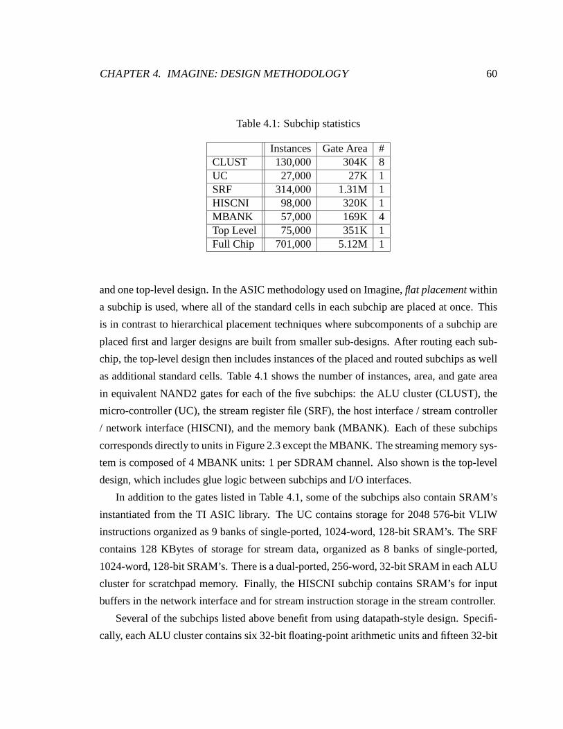
CHAPTER 4. IMAGINE: DESIGN METHODOLOGY 60
Table 4.1: Subchip statistics
Instances Gate Area #CLUST 130,000 304K 8UC 27,000 27K 1SRF 314,000 1.31M 1HISCNI 98,000 320K 1MBANK 57,000 169K 4Top Level 75,000 351K 1Full Chip 701,000 5.12M 1
and one top-level design. In the ASIC methodology used on Imagine, flat placement within
a subchip is used, where all of the standard cells in each subchip are placed at once. This
is in contrast to hierarchical placement techniques where subcomponents of a subchip are
placed first and larger designs are built from smaller sub-designs. After routing each sub-
chip, the top-level design then includes instances of the placed and routed subchips as well
as additional standard cells. Table 4.1 shows the number of instances, area, and gate area
in equivalent NAND2 gates for each of the five subchips: the ALU cluster (CLUST), the
micro-controller (UC), the stream register file (SRF), the host interface / stream controller
/ network interface (HISCNI), and the memory bank (MBANK). Each of these subchips
corresponds directly to units in Figure 2.3 except the MBANK. The streaming memory sys-
tem is composed of 4 MBANK units: 1 per SDRAM channel. Also shown is the top-level
design, which includes glue logic between subchips and I/O interfaces.
In addition to the gates listed in Table 4.1, some of the subchips also contain SRAM’s
instantiated from the TI ASIC library. The UC contains storage for 2048 576-bit VLIW
instructions organized as 9 banks of single-ported, 1024-word, 128-bit SRAM’s. The SRF
contains 128 KBytes of storage for stream data, organized as 8 banks of single-ported,
1024-word, 128-bit SRAM’s. There is a dual-ported, 256-word, 32-bit SRAM in each ALU
cluster for scratchpad memory. Finally, the HISCNI subchip contains SRAM’s for input
buffers in the network interface and for stream instruction storage in the stream controller.
Several of the subchips listed above benefit from using datapath-style design. Specifi-
cally, each ALU cluster contains six 32-bit floating-point arithmetic units and fifteen 32-bit

CHAPTER 4. IMAGINE: DESIGN METHODOLOGY 61
Floorplan
LocalNetlists
Library
ShortWire
Models
Place &Route
Structure
Layout
ExtractorR & CTiming
AnalysisSlowPaths
ManualDesign
RTLStructured
RTL
Regions
Wire plan Key WiresPlacement& Loads
Synthesis
Figure 4.2: Tiled Region Design Methodology
register files. Exploiting the datapath regularity for these units keeps wire lengths within
a bitslice very short, which in turn leads to smaller buffers, and therefore a more compact
design. In addition, control wires are distributed across a bitslice very efficiently since cells
controlled by the same control wires can be optimally aligned. The SRF, which contains
22 8-entry 256-bit streambuffers, also benefits from the use of datapaths. The 256 bits in
the streambuffers align to the 8 clusters’ 32-bit-wide datapath, keeping wires predictable
and short and allowing for efficient distribution of control wires.
The tiled-region basic flow used on Imagine is shown in Figure 4.2. It is similar to the
typical ASIC methodology shown previously in Figure 4.1. However, several key addi-
tional steps, shown in gray, have been added in order to allow for datapath-style placement
and to reduce costly design iterations. First, in order to make sure that datapath structure
is maintained all the way through the flow, two RTL models were used. A second RTL
model, labeled structured RTL, was written. It is logically equivalent to the behavioral
RTL, but contains additional logical hierarchy in the RTL model. Datapath units such as
adders, multipliers, and register files contain submodules that correspond to datapath bit-
slices. These bitslices correspond to a physical location along the datapath called a region.
Regions provide a hard boundary during placement, meaning cells assigned to that region
will only be placed within the associated datapath bitslice. Regions are often used in typical

CHAPTER 4. IMAGINE: DESIGN METHODOLOGY 62
ASIC design methodologies in order to provide constraints on automatic place and route
tools, but the tiled-region flow has a much larger number of smaller regions (typically 10
to 50 instances per region) when compared to timing-driven placement flows.
In addition to the floorplanning of regions, the subchip designer also must take into
account the wire plan for a subchip. The wire plan involves manually annotating all wires
of length greater than one millimeter with an estimated capacitance and resistance based
on wire length between regions. By using these manual wire-length annotations during
synthesis and timing analysis runs, statistical wire models generated during synthesis are
restricted to short wires. Manual buffers and repeaters were also inserted in the structured
RTL for long wires. With wire planning, pre-placement timing more closely matches post-
placement timing with annotated wire resistance and capacitance.
A more detailed view of the floorplanning and placement portion of the tiled-region
methodology is shown in Figure 4.3. Consider an 8-bit adder. It would be modeled with
the statement y = a + b in behavioral RTL. However, the structured RTL is split up by hand
into bitslices as shown in Figure 4.3. The structured RTL is then either mapped by hand
or synthesized into a standard-cell netlist using Synopsys Design Compiler [Synopsys,
2000a].
In conjunction with the netlist generation, before placement can be run, floorplanning
has to be completed. In the tiled-region design methodology, this is done by writing a
tile file. An example tile file containing two 8-bit adders is shown in the upper right of
Figure 4.3. The tile file contains a mapping between logical hierarchy in the standard cell
netlist and a bounding box on the datapath given in x-y coordinates. The example tile file
shows how the eight bitslices in each adder would be tiled if the height of each bitslice
was 30 units. Arbitrary levels of hierarchy are allowed in a tile file, allowing one to take
advantage of modularity in a design when creating the floorplan. In this example, two levels
of hierarchy are used, so cells belonging to the adder 1/slice5 region would be placed in
the bounding box given by 40 < x < 80 and 150 < y < 180.
Once the floorplan has been completed using a tile file, it is then passed through a tool
developed by Stanford called tileparse. Tileparse flattens the hierarchy of the tile file and
outputs scripts which are later run by the placer to set up the regions. Once the regions
have been set up, but before running placement, the designer can look at the number of
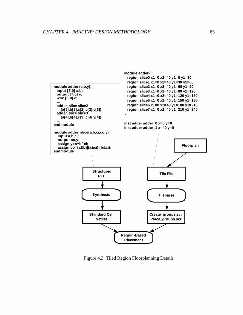
CHAPTER 4. IMAGINE: DESIGN METHODOLOGY 63
module adder (a,b,y); input [7:0] a,b; output [7:0] y; wire [6:0] c; … adder_slice slice2 (a[3],b[3],c[2],c[3],y[3]); adder_slice slice3 (a[4],b[4],c[3],c[4],y[4]); …. endmodule
module adder_slice(a,b,ci,co,y) input a,b,ci; output co,y; assign y=a^b^ci; assign co=(a&b)|(a&ci)|(b&ci); endmodule
Module adder { region slice0 x1=0 x2=40 y1=0 y1=30 region slice1 x1=0 x2=40 y1=30 y1=60 region slice2 x1=0 x2=40 y1=60 y1=90 region slice3 x1=0 x2=40 y1=90 y1=120 region slice4 x1=0 x2=40 y1=120 y1=150 region slice5 x1=0 x2=40 y1=150 y1=180 region slice6 x1=0 x2=40 y1=180 y1=210 region slice7 x1=0 x2=40 y1=210 y1=240 }
inst adder adder_0 x=0 y=0 inst adder adder_1 x=40 y=0
Synthesis
StructuredRTL
Tile File
Floorplan
Standard CellNetlist
Tileparse
Create_groups.scrPlace_groups.scr
Region-BasedPlacement
Figure 4.3: Tiled Region Floorplanning Details
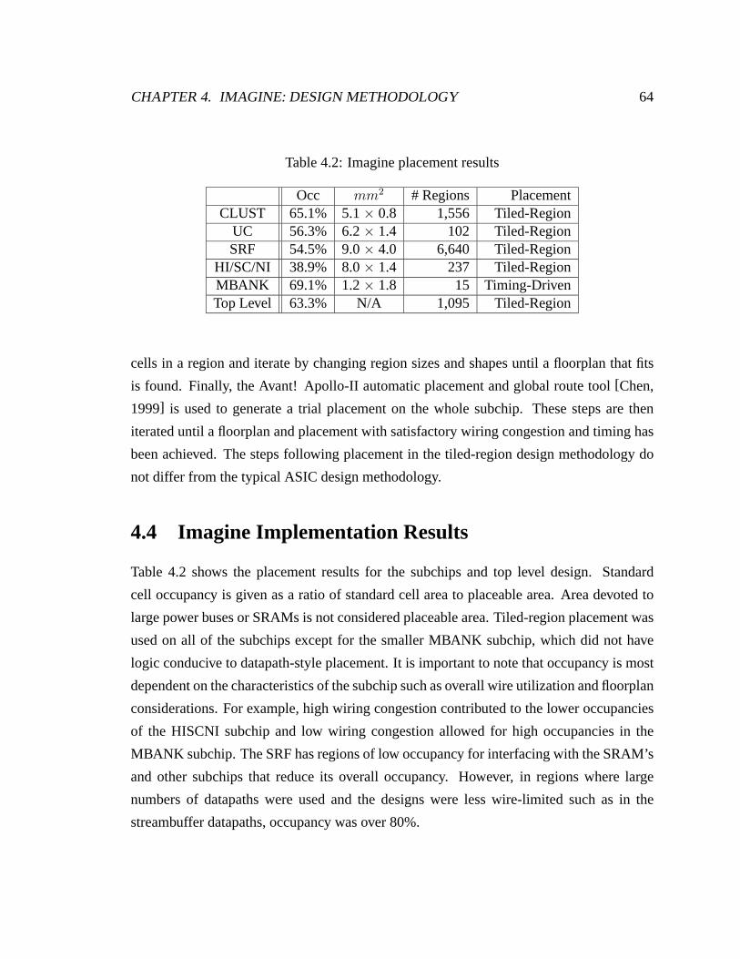
CHAPTER 4. IMAGINE: DESIGN METHODOLOGY 64
Table 4.2: Imagine placement results
Occ mm2 # Regions PlacementCLUST 65.1% 5.1 × 0.8 1,556 Tiled-Region
UC 56.3% 6.2 × 1.4 102 Tiled-RegionSRF 54.5% 9.0 × 4.0 6,640 Tiled-Region
HI/SC/NI 38.9% 8.0 × 1.4 237 Tiled-RegionMBANK 69.1% 1.2 × 1.8 15 Timing-DrivenTop Level 63.3% N/A 1,095 Tiled-Region
cells in a region and iterate by changing region sizes and shapes until a floorplan that fits
is found. Finally, the Avant! Apollo-II automatic placement and global route tool [Chen,
1999] is used to generate a trial placement on the whole subchip. These steps are then
iterated until a floorplan and placement with satisfactory wiring congestion and timing has
been achieved. The steps following placement in the tiled-region design methodology do
not differ from the typical ASIC design methodology.
4.4 Imagine Implementation Results
Table 4.2 shows the placement results for the subchips and top level design. Standard
cell occupancy is given as a ratio of standard cell area to placeable area. Area devoted to
large power buses or SRAMs is not considered placeable area. Tiled-region placement was
used on all of the subchips except for the smaller MBANK subchip, which did not have
logic conducive to datapath-style placement. It is important to note that occupancy is most
dependent on the characteristics of the subchip such as overall wire utilization and floorplan
considerations. For example, high wiring congestion contributed to the lower occupancies
of the HISCNI subchip and low wiring congestion allowed for high occupancies in the
MBANK subchip. The SRF has regions of low occupancy for interfacing with the SRAM’s
and other subchips that reduce its overall occupancy. However, in regions where large
numbers of datapaths were used and the designs were less wire-limited such as in the
streambuffer datapaths, occupancy was over 80%.

CHAPTER 4. IMAGINE: DESIGN METHODOLOGY 65
By using tiled-regioning, large subchips such as the SRF and CLST with logic con-
ducive to datapath-style placement were easily managed by the designer. For example,
placement runs for the SRF, which contained over 300,000 instances took only around one
hour on a 450 MHz Ultrasparc II processor. This meant that when using tiled-region place-
ment on these large subchips, design iterations proceeded very quickly. Furthermore, the
designer had fine-grained control over the placement of regions to easily fix wiring con-
gestion problems. For example, the size and aspect ratio of datapath bitslices could be
modified as necessary to provide adequate wiring resources.
Timing results for each of these subchips are included in Table 4.3. Maximum clock
frequency and critical path for each clock domain in fan-out-of-4 inverter delays (FO4s) are
shown. Results were measured using standard RC extraction and STA tools at the typical
process corner.
4.5 Imagine Clocking Methodology
Most ASIC’s use a tree-based clock distribution scheme. This approach was also used on
Imagine, but distributing a high-speed clock with a large die size and many clock loads
with low skew was challenging. Typical high-performance custom designs use latch-based
design to enable skew tolerance and time-borrowing. However, a large variety of high-
performance latches were not available in Imagine’s standard cell library, so an edge-
triggered clocking scheme where clock skew affects maximum operating frequency was
used. Latches, instead of flip-flops, were used in some register file structures in the ALU
clusters in order to reduce area and power dissipation.
In order to distribute a clock to loads in several subchips while minimizing skew be-
tween the loads, the standard flow in the TI-ASIC methodology was used. First, after each
subchip was placed, a clock tree was expanded within each subchip using available loca-
tions in the floorplan to place clock buffers and wires. Skew between the clock loads was
minimized using Avant! Apollo [Chen, 1999]. Later, when all of the subchips were instan-
tiated in the full-chip design, delay elements were inserted in front of the clock pins for the
subchips so that the insertion delay from the inputs of the delay elements to all of the final
clock loads would be matched for the average insertion delay case. Next, the same flow

CHAPTER 4. IMAGINE: DESIGN METHODOLOGY 66
Table 4.3: Imagine timing results
Clock Max Freq Tcycle (FO4s) Clock Loadsiclk 296 MHz 46.3 160Ksclk 148 MHz 92.6 8.8Khclk 175 MHz 78.3 2.7Kmclk 233 MHz 58.6 19Knclkin 296 MHz 46.3 166nclkout 296 MHz 46.3 55
used on the subchips was used to synthesize a balanced clock tree to all of the inputs of the
delay elements and the leaf-level clock loads for clocked elements in the top-level design.
Imagine must interface with several different types of I/O each running at different
clock speeds. For example, the memory controller portion of each MBANK runs at the
SDRAM clock speed. Rather than coupling the SDRAM clock speed to an integer multiple
of the Imagine core clock speed, completely separate clock trees running at arbitrarily dif-
ferent frequencies were used. In total, Imagine has 11 clock domains: the core clock (iclk),
a clock running at half the core clock speed (sclk), the memory controller clock (mclk), the
host interface clock (hclk), four network input channel clocks (nclkin n, nclkin s, nclkin e,
nclkin w), and four network output channel clocks (nclkin n, nclkout s, nclkout e, nclk-
out w). These clocks and the loads for each clock are shown in Table 4.3, but for clarity,
only one of the network channel clocks is shown. The maximum speed of the network
clocks were architecturally constrained to be the same speed as iclk, but can operate slower
if needed in certain systems. Mclk and hclk are also constrained by the frequency of other
chips in the system such as SDRAM chips, rather than the speed of the logic on Imagine.
Sclk was used to run the SRF and stream controller at half the iclk speed. The relaxed
timing constraints significantly reduced the design effort in those blocks and architectural
experiments showed that running these units at half-speed would have little impact on over-
all performance.
The decoupling provided by Imagine’s 11 independent clock domains reduces the com-
plexity of the clock distribution problem. Also, non-critical timing violations within one
clock domain can be waived without affecting performance of the others. To facilitate these

CHAPTER 4. IMAGINE: DESIGN METHODOLOGY 67
FIFO
ReadPtr
WritePtr
Shift OutRead Clock
Write EnableWrite Clock
Data In Data Out
Sync
Com-pare
Empty
SyncCom-pare
Full
Figure 4.4: Asynchronous FIFO Synchronizer
many clock domains, a synchronizing FIFO was used to pass data back and forth between
different clock domains. Figure 4.4 shows the FIFO design used [Dally and Poulton, 1998].
In this design, synchronization delay is only propagated to the external inputs and outputs
when going from the full to non-full state or vice versa, and similarly with the empty to
non-empty state. Brute force synchronizers were used to do the synchronization. By mak-
ing the number of entries in the FIFO large enough, write and read bandwidths are not
affected by the FIFO design.
4.6 Imagine Verification Methodology
Functional verification of the Imagine processor was a challenge given the limited resources
available in a university research group. A functional verification test suite was written and
run on the behavioral RTL. The same test suite was subsequently run on the structured RTL.
Tests in the suite were categorized either as module-level or chip-level tests. Standard
industry tools performed RTL-to-netlist and netlist-to-netlist comparisons for functional
equivalency using formal methods.
Module-level tests exercised individual modules in isolation. These tests were used
on modules where functionality was well-defined and did not rely on large amounts of
complex control interaction with other modules. Module-level tests that exercised specific

CHAPTER 4. IMAGINE: DESIGN METHODOLOGY 68
corner cases were used for testing Imagine’s floating-point adder, multiplier, divide-square-
root (DSQ) unit, memory controller, and network interface. In each of these units, signifi-
cant random testing was also used. For example, in the memory controller, large sequences
of random memory reads and writes were issued. In addition, square-root functionality in
the DSQ unit was tested exhaustively.
Chip-level tests were used to target modules whose control was highly coupled to other
parts of the chip and for running portions of real applications. Rather than relying only on
end-to-end correctness comparisons in these chip-level tests, a more aggressive compari-
son methodology was used for these tests. A cycle-accurate C++ simulator had already
been written for Imagine. During chip-level tests, a comparison checker verified that the
identical writes had occurred to architecturally-visible registers and memory in both the
C++ simulator and the RTL model. This technique was very useful due to the large number
of architecturally-visible registers on Imagine. Also, since this comparison occurred every
cycle, it simplified debugging since any bugs would be seen immediately as a register-write
mismatch. A number of chip-level tests were written to target modules such as the stream
register file and microcontroller. In order to generate additional test coverage, insertion
of random stalls and timing perturbations of some of the control signals were included in
nightly regression runs.
In total, there were 24 focused tests, 10 random tests, and 11 application portions run
nightly as part of a regression suite. Some focused tests included random timing perturba-
tions. Every night 0.7 million cycles of focused tests, 3.6 million cycles of random tests,
and 1.3 million cycles of application portions were run as part of the functional verification
test suite on the C++ simulator, the behavioral RTL and the structured RTL. These three
simulators ran at 600, 75, and 3 Imagine cycles per second respectively when simulated on
a 750 MHz UltrasparcIII processor.
In summary, the design, clocking, and verification methodologies used on Imagine en-
abled the design of a 0.7M-instance ASIC without sacrificing performance, and with a
considerably smaller design team than comparable industrial designs.

Chapter 5
Imagine: Experimental Results
In this chapter, experimental results measured from the Imagine stream processor are pre-
sented. Imagine was fabricated in a Texas Instruments CMOS process with metal spacing
typical to a 0.18 micron process and with 0.15 micron drawn-gate-length transistors.
Figure 5.1 shows a die photograph of the Imagine processor with the five subchips pre-
sented in Chapter 4 highlighted. Its die size is 16 mm × 16 mm. The IO’s are peripherally
bonded in a 792-pin BGA package. There are 456 signal pins (140 network, 233 memory
system, 45 host, 38 core clock and debug), 333 power pins (136 1.5V-core, 158 3.3V-IO,
39 1.5V-IO), and 3 voltage reference pins. The additional empty area in the chip plot is
either glue logic and buffers between subchips or is devoted to power distribution.
5.1 Operating Frequency
The operating frequency for Imagine was tested on a variety of applications and a range
of core supply voltages. As presented in Chapter 4, static timing analysis tools predicted
Imagine to be fully functional with a clock period of 46 fan-out-of-4 inverter delays, corre-
sponding to 296 MHz operation at the typical process corner at 1.5V and 25◦C. (188 MHz
at the slow process corner, 1.35V, and 125◦C). As shown in Figure 5.2, laboratory mea-
surements for the Imagine processor show significantly slower operation, with a maximum
clock speed of 288 MHz at 2.1V, and a clock speed of only 132 MHz at 1.5V. Package
temperature was monitored during these measurements, and stayed under 40◦C with the
69

CHAPTER 5. IMAGINE: EXPERIMENTAL RESULTS 70
SRF
UC
HI NISC
MB
AN
K0
MB
AN
K1
MB
AN
K2
MB
AN
K3
CLUST1
CLUST0
CLUST3
CLUST2
CLUST5
CLUST4
CLUST7
CLUST6
Figure 5.1: Die Photograph

CHAPTER 5. IMAGINE: EXPERIMENTAL RESULTS 71
50
100
150
200
250
300
1 1.2 1.4 1.6 1.8 2 2.2
Voltage (V)
Fre
que
ncy
(M
Hz)
Predicted
Typical
Worst-case
Measured
Figure 5.2: Measured Operating Frequency
aid of a heat sink and air cooling provided by a fan.
At 288 MHz, Imagine provides a peak performance of 11.5 GFLOPS or 23 16-bit
GOPS, and is able to sustain over 60% of peak performance on some key media processing
applications. However, at 1.5V operation, its clock speed of 132 MHz is less than half as
fast as the 296 MHz typical-corner operation and 30% slower than the slow-corner oper-
ation predicted by static timing analysis tools. Further analysis provides insight into the
source of this discrepancy between predicted and measured performance.
Process variation in both transistors and metal interconnect causes some of the discrep-
ancy. While in an idle state with clocks disabled, an on-chip ring oscillator located near the
periphery of the Imagine die had a measured frequency of 3.13 MHz at 1.5V. In contrast,
timing analysis tools predicted a frequency of 3.48 MHz at the typical process corner and
1.5 V. Since power supply noise and IR drop to the ring oscillator during this measure-
ment would be negligible, this difference suggests there is a frequency degradation of 11%
due solely to process variation in the transistors themselves. However, process variation
in the resistance of metal interconnect and via layers can also exist in modern technology.
This variation is more difficult to measure, but variation in these parameters could also
contribute to a small amount of additional performance degradation.

CHAPTER 5. IMAGINE: EXPERIMENTAL RESULTS 72
0
5
10
15
20
25
30
0.5 0.7 0.9 1.1 1.3 1.5 1.7 1.9 2.1
Voltage (V)
Del
ay (n
s)Cycle Time Scaled Ring Delay
Figure 5.3: Measured Ring Delay
Further insight into reasons for a lower-than-predicted operating frequency can be pro-
vided by comparing the voltage dependence of Imagine’s cycle time to the voltage depen-
dence of the ring oscillator delay. This data is graphed in Figure 5.3. The scaled ring
oscillator delay, shown in the curve on the left, is the ring oscillator delay multiplied by a
constant factor, so that at 1.5 Volts, it equals 3.79ns (for a frequency of 264 MHz). This
delay is what would be expected from static timing analysis given the 11% performance
degradation due to process variation measured on the ring oscillator. Therefore, the scaled
ring oscillator delay shows the cycle time predicted by static timing analysis across a range
of supply voltages.
As other researchers have shown [Chen et al., 1997], the effect supply voltage has on
gate delay in modern CMOS processes where transistors are typically velocity saturated
can be modeled by:
td = kCV
(V − Vth)1.25(5.1)
The measured delay through the ring oscillator follows this gate delay model closely if a
threshold voltage, Vth, of 0.38 Volts is assumed.
CHAPTER 5. IMAGINE: EXPERIMENTAL RESULTS 73
On the other hand, the measured cycle time, shown in the curve on the right in Fig-
ure 5.3, shows voltage adversely affecting delay at significantly higher voltages and in fact,
Imagine stops functioning correctly below 1.2 Volts. At 1.5 Volts, the actual cycle time
is twice the delay predicted by the scaled ring oscillator delay. However, this relative dif-
ference is greater for lower voltages and smaller for higher voltages. For example, at 1.2
Volts, the difference is 3x and at 2.0 Volts, the difference is 1.28x.
Several factors could explain the discrepancies between predicted and measured cy-
cle times. First, internal IR drop across large wire resistances in the the core power supply
could contribute to significantly lower voltages at standard cells located on critical paths. In
addition, if IR drop led to low supply voltages for gates with feedback elements or circuits
that have delays not accurately modeled by (5.1), then their performance at low voltages
could be degraded more severely than the ring oscillator, and they could even stop function-
ing correctly. Finally, the lack of sufficient bypass capacitance on the power supply in areas
of the chip with highly varying current draw could lead to additional supply degradation not
modeled by IR drop and could further degrade performance. These factors could explain
the measured cycle time’s steep slope at voltages significantly higher than that predicted
by the ring oscillator delay measurements. Unfortunately, without sophisticated measure-
ment techniques, it is difficult to conclusively verify the exact factors contributing to this
behavior. Nevertheless, if thorough analysis and careful re-design of the on-chip power
distribution network were able to solve the discrepancy between predicted and measured
operating frequency, at worst-case operating conditions a 1.42x performance improvement
without increasing voltage or degrading energy efficiency would be observed. By improv-
ing to typical operating conditions, a 2x performance improvement over current behavior
would be achieved.
5.2 Power Dissipation
In addition to performance, a processor’s power dissipation is a very important charac-
teristic in many media processing systems. Figure 5.4 shows Imagine’s core total power
dissipation as the core power supply is varied from 1.2 to 2.1 Volts, assuming operating

CHAPTER 5. IMAGINE: EXPERIMENTAL RESULTS 74
0
2
4
6
8
10
12
14
1 1.2 1.4 1.6 1.8 2 2.2
Voltage (V)
Po
wer
(W)
Figure 5.4: Measured Core Power Dissipation
frequencies from Figure 5.2. The core power dissipation was measured during a test appli-
cation written to keep Imagine fully occupied with floating-point arithmetic instructions.
Imagine’s power dissipation is dominated by dynamic power dissipation, given by:
P = CswV 2f
where Csw is the average capacitance switched per clock cycle. At 1.5 Volts and 132 MHz,
a power dissipation of 3.07 Watts was observed, meaning that Csw, the average capacitance
switched per clock cycle, was measured to be 10.3 nF.
Although it is difficult to determine exactly how this 10.3 nF of Csw is distributed
throughout Imagine, estimates can be made with Synopsys Design Compiler [Synopsys,
2000a] using exact capacitances and resistances extracted from actual layout and toggle
rates captured from a test application. These estimates are presented in the pie chart in
Figure 5.5 and sum to the 10.3 nF measured experimentally. Total power dissipation is
separated into three major categories: clock, arithmetic clusters, and other. Clock power
includes capacitance switched during idle operation when only the Imagine core clock is
toggling, and is further subdivided into three categories: Csw in the clock tree, Csw in the
loads of the clock tree, and Csw internally within the flip flops. Together, clock power

CHAPTER 5. IMAGINE: EXPERIMENTAL RESULTS 75
Clock Tree11%
Clock Loads14%
Flip Flop Internal Power29%
Cluster ALUs19%
Cluster RFs, Wires, and Control
21%
SRF, UC, Mbanks6%
Figure 5.5: Csw distribution during Active Operation
comprises around 55% of the total core power, verified experimentally by idle power mea-
surements. The arithmetic cluster power is also subdivided into two categories: capac-
itance switched in the ALUs and capacitance switched elsewhere in the cluster such as
in the LRFs and intracluster switch. The final remaining category labeled SRF, UC, and
Mbanks includes the switched capacitance not accounted for in the arithmetic clusters or
clock network.
Note that on Imagine, a large percentage of power dissipation is devoted to arithmetic
units. Not only is 20% of active power dissipated in the ALUs, but over one third of
the internal flip flop clock power and clock load power is in pipeline registers within the
ALUs. In total, nearly 40% of the chip power is spent directly on providing high-bandwidth
arithmetic units. Furthermore, power dissipation could be significantly reduced by lower-
ing clock power. Lowering the number of pipeline registers or using latch-based clocking
methodologies and more efficient clock trees as would typically be done with custom de-
sign methodologies would help to greatly reduce Imagine’s core power dissipation.

CHAPTER 5. IMAGINE: EXPERIMENTAL RESULTS 76
0
200
400
600
800
1 1.2 1.4 1.6 1.8 2 2.2
Voltage (V)
En
erg
y E
ffic
ien
cy (p
J/O
p)
Figure 5.6: Measured Energy Efficiency
5.3 Energy Efficiency
Although absolute power dissipation for a processor is important since processors in em-
bedded systems often have fixed power budgets, another important metric is energy effi-
ciency, evaluated here as GOPS per Watt or Joules per operation. This metric corresponds
to the energy which must be provided by an external source such as a battery in order to
accomplish a fixed task, such as encoding one frame of video.
The sustained energy efficiency on Imagine, as picoJoules per arithmetic operation,
is shown in Figure 5.6. At the nominal 1.5 Volt supply, Imagine dissipates 363 pJ per
operation (2.4 GFLOPS/W). However, by operating Imagine at lower frequencies and lower
supply voltages, its energy efficiency is improved [Chandrakasan et al., 1994; Horowitz
et al., 1994; Burd and Brodersen, 1995]. Since energy efficiency is given by the ratio
of performance to power (GOPS/W), as supply voltage approaches transistor threshold
and delay increases, operating frequency and performance decrease. However, power is
decreasing at a much faster rate, given by the product of voltage squared and operating
frequency. At its most energy-efficiency condition (1.2 Volt supply), Imagine is 27% more
energy-efficient than at the nominal supply voltage, dissipating only 265 pJ per operation.
Below 1.2 Volts, the chip stops functioning correctly.

CHAPTER 5. IMAGINE: EXPERIMENTAL RESULTS 77
Table 5.1: Energy-Efficiency Comparisons
Processor Volts Tech Data- Peak Power Energy/Optype Performance (W) (pJ)
Intel Pentium 4 1.5 0.13µ FP 12 GFLOPS 80 6700(3.08 GHz) 16b 24 GOPS 80 3350SB-1250 1.2 0.15µ FP 12.8 GFLOPS 10 780(800 MHz) 64b 6.4 GOPS 10 1560
16b 12.8 GOPS 10 780
TI C67x (225 MHz) 1.2 0.13µ FP 1.35 GFLOPS 1.2 889TI C64x (600 MHz) 1.2 0.13µ 16b 4.8 GOPS 0.72 150
Nvidia GeForce3 1.5 0.15µ 8-16b 1200 GOPS 12 10
Imagine 1.5 0.15µ FP 5.3 GFLOPS 3.1 587(132 MHz) 32b 5.3 GOPS 3.1 587
16b 10.6 GOPS 3.1 293Imagine Low-Voltage 1.2 0.15µ FP 2.5 GFLOPS 1.1 423(66 MHz) 32b 2.5 GOPS 1.1 423
16b 5.0 GOPS 1.1 220Imagine Normalized 1.2 0.13µ FP 6.1 GFLOPS 2.0 328to 0.13µ (150 MHz) 32b 6.1 GOPS 2.0 328
16b 12.2 GOPS 2.0 164
To put these numbers in perspective, an energy-efficiency comparison between Imag-
ine and some of media processors presented earlier in Section 2.1 is shown in Table 5.1.
Energy efficiency is shown as energy per arithmetic operation and is calculated from peak
performance and power dissipation. Unlike Section 2.1, here in Table 5.1, energy efficien-
cies are not normalized to the same technology, but rather each processor’s technology and
voltage is listed in the table.
The first section includes two microprocessors, a 3.08 GHz Intel Pentium 41 [Sager
et al., 2001; Intel, 2002] and a Sibyte SB-1250, which consists of two on-chip SB-1 CPU
cores [Sibyte, 2000]. The Pentium 4 is designed for high performance through deep pipelin-
ing and high clock rate. The SiByte processor is targetted specifically for energy efficient
1Gate length for this process is actually 60-70 nanometers because of poly profiling engineering [Tyagi etal., 2000; Thompson et al., 2001].

CHAPTER 5. IMAGINE: EXPERIMENTAL RESULTS 78
operation through extensive use of clock gating and other design techniques for low power.
These processors demonstrate the range of energy efficiencies typically provided by micro-
processors, over 500 pJ per instruction in a 0.13 micron technology.
Digital signal processors are listed next in Table 5.1. The first DSP, the TI C67x [TI,
2003], an 8-way VLIW operating at 225 MHz targets floating-point applications, and has
energy efficiency of 889 pJ per instruction, similar to the SB-1250 when normalized to the
same technology and voltage. The TI C64x [Agarwala et al., 2002], a 600 MHz 8-way
VLIW DSP targeted for lower-precision fixed-point operation, is able to provide improved
energy efficiency over floating-point DSPs at 150-250 pJ per 16b operation. This improved
efficiency is due to arithmetic units optimized for 16b operation and with architectures
designed to efficiently exploit parallelism, such as SIMD operations in the C64x.
Although fixed-point DSPs are able to provide significant improvements over micro-
processors in energy efficiency, special-purpose processors are still one to two orders of
magnitude better, as demonstrated by the Nvidia Geforce3 [Montrym and Moreton, 2002;
Malachowsky, 2002] at 10pJ per operation, or 5 pJ per operation when scaled to 0.13 µm
technology. The energy efficiency of graphics processors is due to their highly parallel ar-
chitectures that provide a large amount of arithmetic performance with low VLSI overhead.
In addition, graphics processors are able to exploit producer-consumer locality by feeding
the output of one stage of the graphics pipeline directly to the next stage of the pipeline,
avoiding global data transfers.
Finally, we present the energy efficiency of Imagine in Table 5.1. When normalized to
the same voltage, Imagine dissipates nearly half the energy per floating-point op per 16-bit
op dissipated by the SB-1250, the most energy efficient fully-programmable floating-point
processor listed. When normalized to the same technology, Imagine provides energy ef-
ficiencies 2.7x better than the C67x on floating-point operations. On 16-bit operations,
Imagine is comparable to the C64x, even though Imagine contains arithmetic units opti-
mized for floating-point and 32-bit performance and a less aggressive design methodology.
In the next section, we will explore the energy efficiency of stream processors optimized for
16-bit fixed-point applications rather than floating-point performance. In addition, we will
demonstrate the potential of stream processors to achieve much higher energy efficiency by
employing more-aggressive custom design methodologies rather than standard cells and by

CHAPTER 5. IMAGINE: EXPERIMENTAL RESULTS 79
Table 5.2: Energy-Delay Comparisons
Processor Volts Tech Data- Energy-Delaytype
Intel Pentium 4 1.5 0.13µ FP 558(3.08 GHz) 16b 140SB-1250 1.2 0.15µ FP 61(800 MHz) 32b 244
16b 611
TI C67x (225 MHz) 1.2 0.13µ FP 658.5TI C64x (600 MHz) 1.2 0.13µ 16b 31Broadcom Calisto 1.2 0.13µ 16b 42.6
Nvidia GeForce3 1.5 0.15µ 8-16b 0.008
Imagine 1.5 0.15µ FP 110(132 MHz) 32b 110
16b 27.6Imagine Normalized 1.2 0.13µ FP 54to 0.13µ (150 MHz) 32b 54
16b 13
using low-power circuit techniques. This would also provide a more fair comparison to the
DSPs and microprocessors listed here, which also use custom design methodologies.
Some researchers have proposed using the energy-delay product as an alternate met-
ric for energy efficiency [Horowitz et al., 1994]. Since processors designed to operate at
slower performance rates can reduce their energy per task with techniques such as smaller
transistor sizing and less pipelining to reduce clock power (at the cost of higher delay per
task), the energy-delay product metric allows one to compare the energy efficiency of two
processors operating at different performance rates.
We evaluated energy-delay product on the same range of processors as shown in Ta-
ble 5.2 (lower energy-delay product is better). As with energy efficiency, energy-delay is
estimated from peak performance and power dissipation, given by the ratio of energy per
operation to the peak performance on that operation type.
The energy-delay product is affected more than energy efficiency or performance alone
by design methodologies and technology scaling. That is because the advantages in raw

CHAPTER 5. IMAGINE: EXPERIMENTAL RESULTS 80
Table 5.3: Sustained Application Performance
Application Operation Performance Core Powertypes (GOPS) (W)
MPEG-2 Encode 32b/16b/8b 4.9 3.6QR Decomposition Floating-point 3.4 4.4
Coherent Side-lobe Cancellation Floating-point 2.3 4.5
performance and energy efficiency provided by smaller device sizes and custom circuits
are compounded with energy-delay product. Nevertheless, when normalized to the same
technology, Imagine still is less than half the energy-delay of the most energy-efficient
DSPs on 16b operations. However, on floating-point, it is slightly worse than the SB-1250.
Several factors in the Imagine implementation lead to higher energy-delay products and
energy efficiency than possible with a more optimal implementation of the Imagine archi-
tecture. First, as described in Section 5.1, if at 1.5V Imagine operated at the worst-case
operating conditions predicted by static timing analysis of 188 MHz rather than the mea-
sured frequency of 132 MHz, it would see a 1.42x improvement in performance, without
affecting energy efficiency. This would translate directly to a reduction in energy-delay
product. Furthermore, by using more aggressive design methodologies and low-power
circuit techniques, Imagine could easily operate at much higher frequencies, and could
therefore provide additional reductions in its energy-delay product.
5.4 Sustained Application Performance
In addition to the peak numbers presented above for performance and power dissipation,
Imagine is able to sustain a large percentage of its peak performance on most media ap-
plications. Using a PCI board containing an Imagine processor running at 144 MHz and
1.5 Volts2, a PowerPC host processor running at 150 MHz, and a 66 MHz bus between
the host processor and Imagine, Imagine sustained the application performance and power
dissipation shown in Table 5.3. Imagine is able to sustain between 40% and 60% of peak
2This frequency is achievable at 1.5 Volts using the software workaround to the worst critical paths.

CHAPTER 5. IMAGINE: EXPERIMENTAL RESULTS 81
performance on these applications.
5.5 Summary
A prototype Imagine processor has been shown to provide a peak performance of 11.5
GFLOPS at its maximum frequency and to dissipate 423 pJ per floating-point operation
at its most energy-efficient operating condition, more than twice as efficient as other pro-
grammable floating-point processors when normalized to the same technology. However,
there is still a large gap in performance, area efficiency, and energy-efficiency of stream
processors when compared to special-purpose processors, typically less than 10 pJ per op-
eration in a 0.13 µm technology. Stream processors have the potential to further close this
gap by utilizing more aggressive custom design methodologies and utilizing low-power
circuit techniques and energy-efficient ALU designs for 16-bit operations. In the next sec-
tion, we extend stream processors to custom design methodologies and stream processors
tailored for low-power embedded systems, demonstrating the potential for highly area- and
energy-efficient stream processors.

Chapter 6
Stream Processor Scalability: VLSI
Costs
The previous chapters in this thesis describe the VLSI implementation and evaluation of
the Imagine stream processor, and demonstrated its capability of efficiently supporting 48
ALUs in a 0.15 µm standard cell technology. In the following chapters, we extend this work
by exploring the capability of scaling stream processors to many more ALUs per chip in
future technologies and by exploring efficiency improvements with more aggressive design
methodologies.
With CMOS technology scaling and improved design methodologies, increasing num-
bers of ALUs can fit onto one chip. On the Imagine stream processor, a multiplier support-
ing single-precision floating-point, 32-bit integer, and dual 16-bit integer multiplies has an
area of 0.486 mm2 (1224K grids) and an average energy per multiply of 185 pJ, includ-
ing internal flip-flop power in pipeline registers. In comparison, custom implementations
of similar multipliers scaled to the same technology would have an area of less than 0.26
mm2 (655K grids) and energy of less than 50 pJ per multiply [Huang and Ercegovac, 2002;
Nagamatsu et al., 1990]. By only supporting 16-bit data-types, this custom multiplier area
and energy could be further reduced to less than 15pJ [Goldovsky et al., 2000]. Other com-
ponents, such as register files, scale similarly to custom methodologies. This demonstrates
the potential for large area and energy savings by employing custom design methodologies,
rather than standard cells, and by tailoring datapaths to smaller widths if that is all that is
82

CHAPTER 6. STREAM PROCESSOR SCALABILITY: VLSI COSTS 83
required by the application. Furthermore, available on-chip arithmetic bandwidth increases
by 70% each year [Dally and Poulton, 1998]. In a 45 nanometer technology, expected to
be available by the end of the decade [SIA, 2001], the Imagine multiplier would scale to
0.044 mm2. In this technology, over two thousand of these multipliers could fit on a single
1 cm2 chip and could be easily pipelined to operate at over 1 GHz. At this speed, these
multipliers could provide 2 Teraops per second of arithmetic bandwidth.
Although technology scaling and custom design methodologies provide the potential
for thousands of ALUs per processor in the future technologies, conventional proces-
sor architectures do not scale effectively. Agarwal et al. studied the scaling of general-
purpose microprocessors and showed that the performance of conventional superscalar mi-
croprocessors will be limited by wire delay and large global structures in future technolo-
gies [Agarwal et al., 2000]. As a result, these microprocessors, which historically have
been scaling at 50-60% annually, will be limited to 12.5% annual performance improve-
ments when scaling from a 250 nanometer to 35 nanometer technology.
Furthermore, Rixner et al. studied the VLSI efficiencies of the register organizations in
a variety of processors [Rixner et al., 2000b]. A conventional processor with a inefficient
single unified register file, for example, would have a support structure that would dwarf
the area and power of the ALUs themselves. Stream processors, on the other hand, are area-
and energy-efficient, primarily due to their partitioned register file structure, as described
in Section 2.4.4.
In the remainder of this chapter, the feasibility of scaling stream processors to thousands
of ALUs is explored. We develop a cost model that estimates the area, delay, and energy of
a stream processor as a function of C the number of clusters and N the number of ALUs per
cluster. We use these models to evaluate intercluster scaling (increasing C) and intracluster
scaling (increasing N ). Our analysis shows that scaling to hundreds of clusters with tens
of ALUs per cluster incurs only modest penalties for energy and area. For example, a 640-
ALU C = 128 N = 5 stream processor requires only 2% more area per ALU and only 7%
more energy per ALU operation than a 40-ALU C = 8 N = 5 stream processor.

CHAPTER 6. STREAM PROCESSOR SCALABILITY: VLSI COSTS 84
Table 6.1: Building Block Areas, Energies, and Delays
Param Description ValueASRAM Area of 1 bit of SRAM used for SRF or Microcontroller
(grids)16.1
ASB Area per SB width (grids) 2200wALU Datapath width of an ALU (tracks) 880wLRF Datapath width of LRFs required per ALU (tracks) 440wSP Scratchpad datapath width (tracks) 710h Cluster datapath height (tracks) 1400v0 Wire propagation velocity in tracks per FO4 1400tcyc FO4s per clock 45tmux Delay of 2:1 mux in FO4s 2Ew Normalized wire propagation energy per track 1
EALU Energy of ALU operation (normalized to Ew) 2.0 × 10⁶
ESRAM SRAM access energy per bit (normalized to Ew) 8.7ESB SB access energy per bit (normalized to Ew) 1900ELRF LRF access energy (normalized to Ew) 8.9 × 10⁵
ESP SP access energy (normalized to Ew) 1.6 × 10⁶
T Memory latency (cycles) 55b Data width of the architecture 32
6.1 VLSI Cost Models
The area, delay, and energy of a stream processor can be modeled by constructing a pro-
cessor from a small set of basic building blocks: four types of on-chip memory (SRAMs,
SPs, LRFs, and streambuffers), ALUs, and switches (wires). The SRAM area and energy
is taken from a large single-ported SRAM macro whereas the SP memory is taken from
a dual-ported memory. The LRFs and streambuffers were implemented with standard-cell
latches and flip flops. The ALUs were implemented with standard-cell logic functions.
The area, delay, and energy of these basic building blocks, measured from the Imagine
processor, are presented in Table 6.1. Area and energy measurements are normalized to
process-independent values. For example, area values are normalized to units of minimum
wire grids (0.40 square microns in the 0.18 micron technology used for Imagine). Energy
values are normalized to Ew, the propagation energy for a minimum-width wire per wire

CHAPTER 6. STREAM PROCESSOR SCALABILITY: VLSI COSTS 85
Table 6.2: Scaling Coefficients
Param Description ValueGSRF Width of SRF bank per N (words) 0.5GSB Average number of SB accesses per ALU operation in typical kernels 0.2
GCOMM COMM units required per N 0.2GSP SP units required per N 0.2I0 Initial width of VLIW instructions (bits) 196IN Additional VLIW instruction width per function unit 40LO Required number of non-cluster SBs 6LC Initial number of cluster SBs 6LN Additional SBs required per N 0.2rm SRF capacity needed per ALU for each cycle of memory latency
(words)20
ruc Number of VLIW instructions required in microcode storage 2048
C Arithmetic clusters —N Number of ALUs per cluster —
track of length (0.093 fJ per wire track in a 0.18 micron technology1). Measured delays
for on-chip wire propagation and key gates which will be used to construct large switches
are presented in fan-out-of-4 inverter delays (FO4s), a process-independent measure of
device speed. As technology scales, wire propagation velocity v0 stays relatively constant
with optimal repeatering [Ho et al., 2001]. A clock cycle of 45 FO4s, measured from
the Imagine stream processor, was used. Typical microprocessors designed with custom
methodologies have clock cycles closer to 20 FO4s [Agarwal et al., 2000]. Adapting the
cost analysis to results for custom processors will be addressed in Section 6.3.
A stream processor can be constructed from the building blocks in Table 6.1. However,
appropriate sizes and bandwidths must be chosen for structures such as the local register
files, stream register file, microcontroller, and others. The values shown in Table 6.2 were
used to govern how such structures should scale. These values were empirically determined
from the inner loop characteristics of a variety of key media processing kernels, shown in
1Calculated from an assumed wire capacitance of 0.26 fF per micron including repeater capacitance [Hoet al., 2001] with a 25% 1-to-0 transition probability.
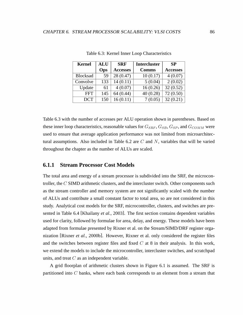
CHAPTER 6. STREAM PROCESSOR SCALABILITY: VLSI COSTS 86
Table 6.3: Kernel Inner Loop Characteristics
Kernel ALU SRF Intercluster SPOps Accesses Comms Accesses
Blocksad 59 28 (0.47) 10 (0.17) 4 (0.07)Convolve 133 14 (0.11) 5 (0.04) 2 (0.02)
Update 61 4 (0.07) 16 (0.26) 32 (0.52)FFT 145 64 (0.44) 40 (0.28) 72 (0.50)
DCT 150 16 (0.11) 7 (0.05) 32 (0.21)
Table 6.3 with the number of accesses per ALU operation shown in parentheses. Based on
these inner loop characteristics, reasonable values for GSRF , GSB , GSP , and GCOMM were
used to ensure that average application performance was not limited from microarchitec-
tural assumptions. Also included in Table 6.2 are C and N , variables that will be varied
throughout the chapter as the number of ALUs are scaled.
6.1.1 Stream Processor Cost Models
The total area and energy of a stream processor is subdivided into the SRF, the microcon-
troller, the C SIMD arithmetic clusters, and the intercluster switch. Other components such
as the stream controller and memory system are not significantly scaled with the number
of ALUs and contribute a small constant factor to total area, so are not considered in this
study. Analytical cost models for the SRF, microcontroller, clusters, and switches are pre-
sented in Table 6.4 [Khailany et al., 2003]. The first section contains dependent variables
used for clarity, followed by formulae for area, delay, and energy. These models have been
adapted from formulae presented by Rixner et al. on the Stream/SIMD/DRF register orga-
nization [Rixner et al., 2000b]. However, Rixner et al. only considered the register files
and the switches between register files and fixed C at 8 in their analysis. In this work,
we extend the models to include the microcontroller, intercluster switches, and scratchpad
units, and treat C as an independent variable.
A grid floorplan of arithmetic clusters shown in Figure 6.1 is assumed. The SRF is
partitioned into C banks, where each bank corresponds to an element from a stream that

CHAPTER 6. STREAM PROCESSOR SCALABILITY: VLSI COSTS 87
ClusterSRFClusterSRF
ClusterSRFClusterSRF
ClusterSRFClusterSRF
Micro-Controller
C1/2NCOMMb
C1
/2N
CO
MMb
Figure 6.1: Scalable Grid Floorplan
a cluster will read during SRF reads and writes. The only communication between the
clusters or SRF banks is in the memory system ports to the SRF (not shown) and the
intercluster switch, with buses and cross-point switches represented as lines and dots in
Figure 6.1.
Stream Register File
The area of the SRF, ASRF , contains two components: the stream storage and the stream-
buffers (SBs). The SRF is used to stage streams passed between kernels. A SB automati-
cally prefetches sequential data for its associated stream out of the stream storage. All SBs
share a single port into the stream storage, allowing that single port to act as many logi-
cal ports. The stream storage is a large single-ported on-chip SRAM, organized as rmTN

CHAPTER 6. STREAM PROCESSOR SCALABILITY: VLSI COSTS 88
blocks of C banks, for a total capacity of rmTNC words. This capacity is necessary to
cover external memory latency. In a fixed technology, since the area and access energy of
the stream storage grow linearly with the capacity, both the area and energy grow linearly
with the number of ALUs in a stream processor.
Each SB contains storage for two blocks of the SRF to act as a double-buffer for cov-
ering the latency of block reads and writes from the stream storage. Each SRF bank has
a block width of GSRF Nb, requiring 2GSRF Nb bits of storage per SB. A total of NSB
streambuffers are required for a given stream processor configuration. As shown in Ta-
ble 6.4, three factors determine the total number of SBs. LO SBs are required for memory,
host, and microcontroller transfers. LC cluster SBs are required to provide an ample num-
ber of input and output streams for typical kernels. Finally, as N increases, more bandwidth
is often required between some of the SBs and the ALUs. This is accounted for with a third
term, LNN . Input or output streams with multi-word records that require more bandwidth
must be split into multiple streams and utilize these additional SBs to keep from becoming
a performance bottleneck2. Asymptotically, the area of the SBs grows with N2, but for
N < 64, the linear term accounts for the majority of the area. The energy dissipated in the
SBs is related to the number of SB accesses per ALU operations, GSB . Half of the accesses
are assumed to be reads and require a traversal of the intracluster switch.
Microcontroller
The microcontroller, listed next in Table 6.4, provides storage for the kernels’ VLIW in-
structions, and sequences and issues these instructions during kernel execution. The mi-
crocode storage is a large single-ported memory. The microcontroller area is comprised of
the microcode storage area and area for control wire distribution between the microcon-
troller and the clusters. The microcode storage requires ruc VLIW instructions for kernel
storage in typical applications. Although as is shown in Section 7.3, increasing N results in
higher inner-loop performance, the number of instructions in a kernel stays relatively con-
stant with N since more loop unrolling is often used with higher N to provide more ILP and
2Splitting multi-word-record streams into multiple streams was done by hand to optimize performancefor the experiments in Section 7.3.

CHAPTER 6. STREAM PROCESSOR SCALABILITY: VLSI COSTS 89
Table 6.4: Scaling Cost Models
Element EquationCOMMs per NCOMM = GCOMMNClusterSPs per cluster NSP = GSP NFUs per cluster NFU = N + NSP + NCOMM
Cluster SBs NCLSB = LC + LNNTotal SBs NSB = LO + NCLSB
External Pe = NCLSB
Cluster Ports
Total Area ATOT = CASRF + AUC + CACLST + ACOMM
SRF Bank Area ASRF = rmTNASRAMb + (2GSRF N)NSBASBbMicrocontroller AUC = ruc(I0 + INNFU)ASRAM+Area (INNFU)
√ASRF + ACLST + ACOMM
Cluster Area ACLST = NFUwLRF h + NwALUh + NSP wSP h + ASW
Intracluster ASW = NFU(√
NFUb)(2√
NFUb + h + 2wALU + 2wLRF )+Switch Area
√NFU(3
√NFUb + h + wALU + wLRF )Peb
Intercluster ACOMM = CNCOMMb√
C(NCOMMb√
C + 2√
ACLST + ASRF )Switch Area
Intracluster tintra =√
NFU(h + 2√
NFUb + wALU + wLRF +√
NFUb)/v0+Wire Delay tmux(log2
√NFU +
√NFU)
Intercluster tinter = tintra + 2√
CACLST + CASRF + ACOMM/v0+
Wire Delay tmux(log2
√CNCOMM +
√C)
Total Energy ETOT = CESRF + EUC + CECLST + GCOMMNCbEinter
SRF Bank ESRF = rmTNbESRAMGSB/GSRF + (GSBNb)(ESB + Eintra/2)EnergyMicrocontroller EUC = ruc(I0 + INNFU)ESRAM+
Energy (INNFU)Ew(√
C√
CASRF + CACLST + ACOMM)Cluster Energy ECLST = NFUELRF + NEALU + GSP NESP + NFUbEintra
Intracluster Eintra = Ew
√NFU((h + 2
√NFUb) + 2(wALU + wLRF +
√NFUb))
Switch EnergyIntercluster Einter = Ew(2
√C)(
√ACLST + ASRF + NCOMMb
√C)
Switch Energy
because loop prologues and epilogues in kernels are critical-path limited, not arithmetic-
bandwidth limited. The width of each VLIW instruction is given by I0 + INNFU bits.
CHAPTER 6. STREAM PROCESSOR SCALABILITY: VLSI COSTS 90
I0 bits are required for microcontroller instruction sequencing, conditional stream instruc-
tions, immediate data, and for interfacing with the SRF. IN bits per ALU per cluster are
required to encode ALU operations, to control LRF read and writes, and to control the
intracluster switch. Area and energy for distributing the instructions from the microcode
storage to the grid of clusters is accounted for in the second term in both formulae in Ta-
ble 6.4. In addition, repeaters and pipeline registers are required within the cluster grid for
more instruction distribution, but this area is accounted for in the area measured for the
components in Table 6.2.
Arithmetic Clusters
Each cluster is comprised of area devoted to the LRFs, ALUs, a scratchpad, and the intra-
cluster switch. This switch is a full crossbar that connects the outputs of the FUs and the
streambuffers to the inputs of the LRFs and the streambuffers. In this study, the ALUs are
assumed to be arranged in a square grid as shown in Figure 6.2, where each row contains
a bus for each ALU output in that row and each column contains a bus for each LRF in-
put in that column. The row-column intersections contain program-controlled cross-point
switches that connect rows to columns. This grid structure minimizes the area and wire
delay of the intracluster switch when the number of ALUs per cluster is large3. The area
devoted to the intracluster switch includes wire tracks for the wires and repeaters in the
rows and columns of the grids and the cross-points between the rows and columns, as
shown in Figure 6.2. Additional area for the external ports from the cluster streambuffers is
included as well. Area from the control wires for the crosspoints is ignored for simplicity
since it is small when compared to the area for the data wires.
Table 6.4 also includes equations for the energy dissipated in an arithmetic cluster4 and
the intracluster wire delay. For wire delay, the first term in Eintra models the worst-case
wire propagation delay incurred in the intracluster switch (width + height of a cluster)/v0
and a term for the logic delay through the cross points. The logic delay includes a√
NFU :1
mux for each row-column to select which ALU to read from on that row, followed by
3For smaller numbers of ALUs per cluster, a linear floorplan has comparable area and delay, but forsimplicity, only grid floorplans are considered in this study.
4ECLST from Table 6.4 includess a correction from [Khailany et al., 2003] for the term modeling energydissipated in the scratchpad.

CHAPTER 6. STREAM PROCESSOR SCALABILITY: VLSI COSTS 91
ALU
RFRF
ALU
RFRF
wALU
h
wLRF
Peb
NFU1/2b
2NFU1/2bPeb
Figure 6.2: Intracluster Switch Floorplan
an additional 2:1 mux delay at each additional row in the column to choose between the
current row or the adjacent rows. As N increases, the VLSI costs of the arithmetic clusters
are dominated by the N3/2FU term in the intracluster switch area.
Intercluster Switch
The final component of the stream processor area is the intercluster switch, shown in Fig-
ure 6.1. Each cluster has NCOMM buses it broadcasts to in the rows and NCOMM buses
it reads from in the columns. Since each cluster can only access stream elements from
its SRF bank, the intercluster switch allows kernels that aren’t completely data parallel to
communicate data with each-other without going back to memory. It is also used by condi-
tional streams to route data to and from the SRF [Kapasi et al., 2000]. A two-dimensional
grid structure similar to the intracluster switch is also assumed for the floorplan of the
arithmetic clusters. This layout minimizes the area, delay, and energy overhead of the in-
tercluster switch when the number of arithmetic clusters becomes large. Each cluster has
NCOMM buses it writes to in each row and reads from in each column, so there is a bus
width of NCOMMb√
C between each arithmetic cluster. As shown in ECOMM , on average,
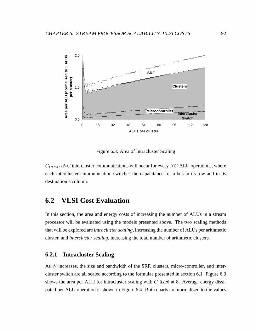
CHAPTER 6. STREAM PROCESSOR SCALABILITY: VLSI COSTS 92
Intercluster Switch
Microcontroller
Clusters
SRF
0.0
1.0
2.0
0 16 32 48 64 80 96 112 128
ALUs per cluster
Are
a p
er A
LU
(n
orm
aliz
ed t
o 5
AL
Us
per
clu
ster
)
Figure 6.3: Area of Intracluster Scaling
GCOMMNC intercluster communications will occur for every NC ALU operations, where
each intercluster communication switches the capacitance for a bus in its row and in its
destination’s column.
6.2 VLSI Cost Evaluation
In this section, the area and energy costs of increasing the number of ALUs in a stream
processor will be evaluated using the models presented above. The two scaling methods
that will be explored are intracluster scaling, increasing the number of ALUs per arithmetic
cluster, and intercluster scaling, increasing the total number of arithmetic clusters.
6.2.1 Intracluster Scaling
As N increases, the size and bandwidth of the SRF, clusters, micro-controller, and inter-
cluster switch are all scaled according to the formulae presented in section 6.1. Figure 6.3
shows the area per ALU for intracluster scaling with C fixed at 8. Average energy dissi-
pated per ALU operation is shown in Figure 6.4. Both charts are normalized to the values

CHAPTER 6. STREAM PROCESSOR SCALABILITY: VLSI COSTS 93
Intercluster Switch
Microcontroller
Clusters
SRF
0.0
1.0
2.0
3.0
0 16 32 48 64 80 96 112 128
ALUs per cluster
En
erg
y d
issi
pat
ed p
er A
LU
op
erat
ion
(no
rmal
ized
to
5 A
LU
s p
er c
lust
er)
Figure 6.4: Energy of Intracluster Scaling
for N = 5, the most area- and energy-efficient configuration. For small N , the overhead
from the I0 bits of microcode storage and the COMM and SP units contributes to larger
area per ALU. The area per ALU then stays within 16% of the minimum up to 16 ALUs
per cluster, at which point the intracluster and intercluster switch start to reduce the area
efficiency. The energy efficiency follows a similar trend, although by 16 ALUs per cluster
the energy per ALU op has grown to 1.22x of the minimum, due to the intracluster switch
and microcontroller instruction distribution to the large arithmetic clusters.
6.2.2 Intercluster Scaling
Compared to intracluster scaling, intercluster scaling incurs more modest VLSI costs be-
cause the intercluster switch grows more slowly than the intracluster switch as the number
of ALUs per processor are increased. Figure 6.5 shows the area per ALU as C is increased
from 8 to 256, assuming a constant cluster size of N = 5. The area per ALU is normal-
ized to the C = 8 N = 5 processor for comparison to stream processors feasible in today’s
technology. The C = 32 processor actually has 3% improved area per ALU over the C = 8
processor as the cost of the micro-code storage is amortized over more clusters. However

CHAPTER 6. STREAM PROCESSOR SCALABILITY: VLSI COSTS 94
Intercluster Switch
Microcontroller
Clusters
SRF
0.0
1.0
2.0
8 16 32 64 128 256
Number of Clusters
Are
a p
er A
LU
(n
orm
aliz
ed t
o 8
cl
ust
ers)
Figure 6.5: Area of Intercluster Scaling
at C = 128, the area per ALU is 2% worse than for C = 8, mostly due to area in the inter-
cluster switch. As shown in Figure 6.6, energy overhead grows slightly faster than area. A
C = 128 dissipates 7% more energy per ALU operation than for C = 8.
6.2.3 Combined Scaling
By combining intercluster and intracluster scaling, configurations with thousands of ALUs
are feasible, as shown in Figure 6.7. The area per ALU is graphed for 2, 5, and 16 ALUs per
cluster with the number of clusters shown on the x-axis. These results show that by scaling
to N = 5, then employing intercluster scaling provides the most area- and energy-efficient
configurations over the range of C from 8 to 128. This is because the additional cost of
supporting more than one port into the intercluster switch hurts area and energy efficiency
standpoint for N > 5. However, it is not prohibitively expensive: the additional cost of
scaling from N = 5 to N = 10 is only 5-11% and 8-13% worse for area and energy per
ALU depending on C.

CHAPTER 6. STREAM PROCESSOR SCALABILITY: VLSI COSTS 95
Intercluster SwitchMicrocontroller
Clusters
SRF
0.0
1.0
2.0
8 16 32 64 128 256
Number of Clusters
En
erg
y d
issi
pat
ed p
er A
LU
op
erat
ion
(no
rmal
ized
to
8 c
lust
ers)
Figure 6.6: Energy of Intercluster Scaling
0.0
1.0
2.0
0 256 512 768 1024
Total ALUs
Are
a p
er A
LU
(n
orm
aliz
ed t
o 3
2 cl
ust
ers,
5 A
LU
s p
er c
lust
er)
N=5
N=16N=2
Figure 6.7: Area of Combined Scaling

CHAPTER 6. STREAM PROCESSOR SCALABILITY: VLSI COSTS 96
As technology enables more ALUs to fit on a single chip, architectures must efficiently
utilize bandwidth in order to achieve large performance gains. Intracluster scaling was
shown to be effective from a cost standpoint up to 10 ALUs per cluster, although was
most area- and energy-efficient at 5 ALUs per cluster. Intercluster scaling was shown to be
effective up to 128 clusters with a slight decrease in area and energy efficiency, although
was most area-efficient at 32 clusters. Together, these two scaling techniques enable area-
and energy-efficient stream processors with thousands of ALUs.
6.3 Custom and Low-Power Stream Processors
Although the preceding analysis used technology parameters typical to a less-aggressive
standard-cell design methodology, the results would be similar for a full-custom design.
Full-custom processors have clock cycles of less than 20 FO4s [Agarwal et al., 2000], but
also have smaller functional units and register files, leading to higher absolute performance
and lower absolute area and energy.
In this section, we demonstrate the effect of design methodologies and operand types
on area and energy efficiency by considering three stream processor types, each with dif-
ferent area, energy, and ALU types, but the same underlying stream architecture. The first
type, ASIC, assumes a standard-cell design methodology, and uses measurements of area,
delay, and energy of key components taken directly from the Imagine stream processor.
The second type, CUST, is functionally equivalent to ASIC, but assumes custom design
methodologies for key blocks, leading to improved area and energy efficiency and clock
frequency. Finally, the third type, LP, is a stream processor targeted for low-power em-
bedded systems that only requires lower-precision fixed-point data-types. It also assumes
full-custom circuits similar to CUST. However, rather than supporting both 32-bit mixed
floating-point/integer ALUs and dual 16-bit operations, LP only supports dual 16-bit fixed-
point fused multiply-add units similar to the DOTP instructions in the Texas Instruments
C64x instruction set [Golston, 2000].
The analytic models presented in the previous section can be used to study the area and
energy efficiency of the ASIC, CUST, and LP configurations. Note that this only models
the area and power in the arithmetic clusters, SRF, and microcontroller. The analysis for

CHAPTER 6. STREAM PROCESSOR SCALABILITY: VLSI COSTS 97
Table 6.5: Building block Areas, Energies, and Delays for ASIC, CUST, and LP
Param Description ASIC CUST LP
wALU Datapath width of an 876.9 1447 (Aggr) 515ALU (tracks) 1918 (Cons)
wLRF Datapath width of LRFs re-quired per ALU (tracks)
437.0 92.1 92.1
wSP Scratchpad datapath width(tracks)
708.9 1551 1551
ASB Area per SB width (grids) 2161.8 230.3 230.3h Cluster datapath height
(tracks)1400 640 640
EALU Average energy of ALU 2.0 × 10⁶ 6.8 × 10⁵ (Aggr) 6.3 × 10⁵
operation (normalized) 2.0 × 10⁶ (Cons)ELRF LRF access energy (normal-
ized)8.9 × 10⁵ 7.9 × 10⁴ 7.9 × 10⁴
ESB SB access energy per bit (nor-malized)
1936 155 155
tcyc FO4s per clock 45 20(Aggr) 4545(Cons)
T Memory latency (cycles) 55 80(Aggr) 5555(Cons)
these units suggests improvements applicable to the full stream processor design through
custom circuit methodologies, however, the analysis is simplified by only studying these
units, which comprise over 70% of the active chip area and power dissipation.
In order to model area and energy costs across the various configurations, it suffices
to vary the area and energy of the building block parameters across the configurations and
then use the analytical models presented it Section 6.1. The parameters that were varied are
presented in Table 6.5, again normalized to technology-independent units. For the ASIC
configuration, the above values are those presented in Table 6.1 taken from the Imagine
stream processor. For the CUST configuration, there are two configurations considered.
The aggressive (Aggr) numbers assume custom cells for ALUs and register files (LRFs
and SBs) whereas the conservative (Cons) only assumes custom cells for register files with

CHAPTER 6. STREAM PROCESSOR SCALABILITY: VLSI COSTS 98
Table 6.6: ASIC, CUST, and LP performance efficiencies
ASIC CUST CONS CUST AGGR LPArea mm2 39.7 32.4 28.4 18.2
(1.2x) (1.4x) (2.2x)Frequency MHz 340 340 770 340Peak Perf GFLOPS 13.7 13.7 30.8 N/A
16b GOPS 27.4 27.4 61.6 54.7Power W 2.8 5.1 3.2 1.2Energy FP pJ/Op @1.2 V 208 161 105 N/AEfficiency 16b pJ/Op @1.2 V 104 81 52 21.5
FP pJ/Op @0.8 V 93 72 47 N/A16b pJ/Op @0.8 V 46 36 23 10
(1.3x) (2.0x) (4.8x)Energy pJ/Op/GFLOPS 15.2 11.8 3.4 N/ADelay pJ/Op/16b GOPS 3.8 3.0 0.85 0.39Product (1.2 V) (1.3x) (4.5x) (9.7x)
the ASIC ALUs. Register file area and energies were taken from custom register files im-
plemented in the same technology as Imagine. ALU data was taken from published 32b
multiplier designs [Huang and Ercegovac, 2002; Nagamatsu et al., 1990]. Note that the
width of various units also changed since a smaller datapath height is assumed with the
custom configuration. Although memories and register files are well documented, it is dif-
ficult to predict exact area and energy of custom ALU designs due to lack of published data,
so carrying out an analysis with both the CUST AGGR and CUST CONS configurations
demonstrates the sensitivity of area and energy to individual ALU designs.
For the LP processor, custom cells were also assumed for both custom ALUs and reg-
ister files. A dual 16b fused-multiply-adder is used with area and energy taken from pub-
lished 16b multipliers [Goldovsky et al., 2000]. Finally, the CUST AGGR configuration is
assumed to have a clock cycle of 20 FO4 inverter delays per cycle, more typical of custom
processors [Agarwal et al., 2000]. This difference in clock cycle time also affects mem-
ory latency, although not exactly by 2.5x since much of the memory latency is incurred
through cycles in the on-chip memory controller. The LP configuration is less aggressively
pipelined than CUST AGGR at 45 FO4 delays per cycle in order to reduce power overhead
CHAPTER 6. STREAM PROCESSOR SCALABILITY: VLSI COSTS 99
in pipeline registers.
Using the models presented in Section 6.1, estimates for area and energy per operation
in the clusters, SRF, and microcontroller were generated. These results are shown in Ta-
ble 6.6, assuming a 1.2 Volt, 0.13 µm technology. In this technology, the minimum wire
pitch is 0.46 µm and a FO4 inverter has a delay of 65 ps. The CUST CONS configuration
is 80% the size of ASIC, due to the smaller LRFs and SBs. Further area reduction occurs
when moving to custom ALUs in the CUST AGGR configuration. The LP configuration
has an additional 36% improvement in area over CUST AGGR because wALU is signif-
icantly smaller, since the 16-bit multiply-add unit only is required to sum half as many
partial products as the multiplier in CUST AGGR. Supporting multiply-add instructions
in the LP configuration also enables twice the peak 16b performance when compared to
CUST CONS.
The energy efficiency savings from moving to custom design methodologies can be
seen when comparing the power of ASIC and CUST AGGR. Although it has 14% higher
power dissipation, CUST AGGR is operating at more than twice the frequency, meaning
that significantly less energy is dissipated per clock cycle. Furthermore, the LP configura-
tion is more than twice as energy-efficient as CUST because each multiply-add operation
consumes less energy but is doing twice the GOPS. Additional energy-efficiency improve-
ments can be achieved in all configurations by operating at a lower voltage. Note that the
energy-efficiencies in Table 6.6 can not be compared directly to other processors, since
they do not take into account other sources of power dissipation in a processor, such as
the clock tree. However, the 4.8x improvement in energy-efficiency suggests that similar
energy savings could be achieved in the clock tree and other parts of the chip by employing
custom design methodologies and using other custom circuit techniques.
These results for custom and low power processors can be further extended by combin-
ing them with the scalability models from Section 6.1 and the technology scaling parame-
ters shown in Table 6.7. The parameters in the top part of the table are based on projections
for future technologies [Ho et al., 2001; SIA, 2001]. The wire capacitance printed assumes
no miller capacitance from adjacent wires, the assumption used for calculating average
case power dissipation. Architectural scaling assumptions are shown in the bottom part of
the table. Since intercluster scaling enables scaling with near-constant area-efficiency, each

CHAPTER 6. STREAM PROCESSOR SCALABILITY: VLSI COSTS 100
Table 6.7: Technology Scaling Parameters
Ldrawn 0.18µm 0.13µm 0.09µm 0.65µm 0.45µm
Volts 1.5 1.2 1.0 0.9 0.9FO4 Delay (ps) 90 65 45 33 23
Wire cap (fF/µm) 0.220 0.212 0.207 0.191 0.178
ALU Clusters 8 16 32 64 128ALUs 40 80 160 320 640
ASIC, LP, CUST CONS 0.25 0.34 0.49 0.68 0.99Frequency (GHz)
CUST AGGR 0.56 0.77 1.1 1.5 2.2Frequency (GHz)
ASIC, CUST CONS 9.9 27.4 79.0 219 632Peak Performance (GFLOPS)
CUST AGGR 22.2 61.6 178 492 1422Peak Performance (GFLOPS)
LP Peak Perf (16b GOPS) 39.5 109 316 875 2528
technology generation allows for a doubling in the number of arithmetic clusters. ALUs
per cluster in Table 6.7 are held constant at 5, the most area- and energy-efficient organiza-
tion. The increase in ALU count with each technology generation can be coupled with an
increase in clock frequency due to decreasing gate delay, allowing for a total improvement
in peak performance of 64x across 5 generations of technology scaling.
The results for area and power scaling across technology generations are shown in Fig-
ure 6.8. Note that the area stays relatively constant for all configurations. With each gen-
eration, approximately twice the number of transistors can fit into the same die area. Since
area-efficiency stays near constant with intercluster scaling, area also stays near constant.
In contrast, power dissipation increases gradually with technology. Although energy effi-
ciency stays near constant with intercluster scaling in the same technology, voltage is not
projected to scale aggressively enough to counteract the additional switched capacitance
with a larger number of clusters.
Energy efficiency scaling is shown in Figure 6.9. For both floating-point and 16b op-
erations, energy efficiency shows dramatic improvements. Since energy-efficiency stays

CHAPTER 6. STREAM PROCESSOR SCALABILITY: VLSI COSTS 101
20
30
40
50
60
70
80
180 130 90 65 45
Technology (nanometers)
Are
a (s
qu
are
mil
lim
eter
s)
ASIC
CUST_CONS
CUST_AGGR
LP
0
5
10
15
180 130 90 65 45
Technology (nanometers)
Po
wer
Dis
sip
atio
n (
W)
ASIC
CUST_CONS
CUST_AGGR
LP
Figure 6.8: Effect of Technology Scaling on Die Area and Power Dissipation

CHAPTER 6. STREAM PROCESSOR SCALABILITY: VLSI COSTS 102
0
40
80
120
160
200
240
180 130 90 65 45
Technology (nanometers)
pJ
per
16b
op
erat
ion ASIC
CUST_CONS
CUST_AGGR
LP
0
50
100
150
200
250
300
350
400
450
500
180 130 90 65 45
Technology (nanometers)
pJ
per
flo
atin
g-p
oin
t o
per
atio
n
ASIC
CUST_CONS
CUST_AGGR
Figure 6.9: Effect of Technology Scaling on Energy Efficiency

CHAPTER 6. STREAM PROCESSOR SCALABILITY: VLSI COSTS 103
near constant with the number of clusters, this improvement is due solely to technology
advances. And since energy efficiency is independent of frequency, it is improving by CV 2
scaling, allowing for an improvement of 29x across five future technology generations.
In summary, by utilizing custom methodologies and fixed-point arithmetic units com-
monly found in DSPs, area and energy efficiency of stream processors can be greatly im-
proved. SRF, microcontroller, and cluster area was shown to be reduced by 30% when
using custom methodologies, while energy efficiency was improved by 2.0x. Energy is
further reduced with dual-16b multiply-add units for an average energy savings of 4.8x
per operation. These area and energy efficiency improvements suggest that total stream
processor efficiency would scale accordingly and would therefore be an order of magni-
tude better in raw performance, performance per unit area, and energy per operation than
current programmable architectures.
Chapter 7
Stream Processor Scalability:
Performance
As presented in the previous chapter, the efficiency of the stream processor register or-
ganization enables scaling to thousands of ALUs providing Teraops per second of peak
performance with only a small degradation in area and power efficiency. However, peak
performance and VLSI efficiency alone does not prove that a stream processor can scale
effectively. Performance efficiency (performance per unit power or performance per unit
area) is achieved by combining VLSI efficiency with high sustained performance.
In this chapter, we evaluate how sustained application and kernel performance scales as
the number of ALUs per stream processor are increased with intracluster and intercluster
scaling. First, we explore how the technology trends of limited off-chip memory bandwidth
and increasing on-chip wire delay affect microarchitecture and performance. Then, we
demonstrate how a stream processor is able to effectively exploit both instruction-level and
data-level parallelism in key media processing kernels and applications to take advantage
of both intracluster and intercluster scaling.
104
CHAPTER 7. STREAM PROCESSOR SCALABILITY: PERFORMANCE 105
7.1 Related Scalability Work
Before presenting the scalability of stream processors, it is worth noting that stream pro-
cessors, like vector processors, are able to exploit both instruction-level and data-level par-
allelism. Therefore, previous work on the scalability of vector processors with media ap-
plications will have some similarities to the studies carried out in this chapter.
Although stream and vector processors share the ability to exploit both instruction-level
and data-level parallelism, they do so with different execution models. Vector microproces-
sors [Kozyrakis, 2002; Wawrzynek et al., 1996] directly execute vector instructions such
as vector adds or multiplies out of a vector register file. This differs from stream proces-
sors, which execute VLIW instructions from a kernel in a SIMD fashion out of a SRF and
contain LRFs to store intermediate results.
Related scalability work in vector processors consists of cost models and sustained
performance on media applications as the number of arithmetic units per processor are
increased. Several authors have analyzed the VLSI costs of components of vector micro-
processors as the number of function units per vector lane is increased [Asanovic, 1998;
Kozyrakis, 2002; Rixner et al., 2000b]. Kozyrakis also analyzed the natural vector lengths
in media benchmarks and the performance of vector microprocessors as the number of
FUs per vector lane are increased [Kozyrakis and Patterson, 2002]. These studies demon-
strate the scalability of vector processors on media applications to tens of arithmetic units
per processor using 8 vector lanes. However, to our knowledge, no previously published
studies explore VLSI costs or performance as vector microprocessors are scaled to greater
than 8 or 16 vector lanes. In the remainder of this chapter, similar scalability studies are
applied to the stream processor model, demonstrating the scalability of stream processors
to hundreds of arithmetic units per processor and leading to different tradeoffs between
instruction-level and data-level parallelism.

CHAPTER 7. STREAM PROCESSOR SCALABILITY: PERFORMANCE 106
7.2 Technology Trends
7.2.1 Memory Bandwidth
In order for a stream processor to effectively scale to hundreds of arithmetic units by the
end of the decade, there must be enough memory bandwidth available for media application
requirements. Fortunately, due to the advent of high-bandwidth memory systems and high
compute intensity in media appliations, hundreds of arithmetic units could be supported in
future technologies without media applications becoming memory limited.
While available on-chip arithmetic bandwidth is increasing at 70% annually, off-chip
pin bandwidth is only increasing by 25% each year [Dally and Poulton, 1998] if only
standard scaling techniques are used. As explained in Section 2.4, Imagine deals with
this bandwidth gap by mapping stream programs onto a three-tiered bandwidth hierarchy
and by efficiently exploiting locality. Producer-consumer locality is exploited by passing
streams between kernels through the second tier of the bandwidth hierarchy, the SRF. Ker-
nel locality is exploited by keeping all temporary data accesses during kernel execution in
the LRFs within the arithmetic clusters, the third tier of the hierarchy. Using these tech-
niques, Imagine is able to sustain high arithmetic performance with significantly lower
off-chip bandwidth. Imagine contains 40 fully-pipelined ALUs and at 232 MHz, provides
2.3 GB/s of external memory bandwidth, 19.2 GB/s of SRF bandwidth, and 326.4 GB/s of
LRF bandwidth. This bandwidth hierarchy on Imagine provides a ratio of ALU operations
to memory words referenced of 28.
Although Imagine can execute applications with compute intensities of greater than
28 without becoming memory-bandwidth limited, this threshold would increase for future
stream processors as off-chip bandwidth grows more slowly than arithmetic bandwidth.
Assuming the scaling factors for arithmetic and off-chip bandwidth above, this threshold
will grow at 36% annually, meaning if stream processors arithmetic performance increased
at 70% annually, in five years, applications with compute intensities of less than 130 would
be memory-bandwidth limited. Fortunately, with the advent of memory systems optimized
for bandwidth and the large and growing compute intensity of media applications, this

CHAPTER 7. STREAM PROCESSOR SCALABILITY: PERFORMANCE 107
problem can be mitigated. For example, a stream processor with a 16 GB/s memory sys-
tem, achievable with eight Rambus channels [Rambus, 2001], could support 400 1 GHz
arithmetic units without being memory-bandwidth limited on applications requiring greater
than 100 operations per memory reference. This suggests that the bandwidth hierarchy in
stream processors should be able to scale effectively to hundreds of ALUs and provide
large speedups without becoming memory bandwidth limited.
7.2.2 Wire Delay
Not only is memory bandwidth becoming even more of a scarce resource in modern VLSI
technology, but another issue facing modern microarchitecture is on-chip wire delay. As
technology has scaled, wire resistance per unit length has been increasing while gate delay
has been decreasing [Ho et al., 2001]. These trends are projected to continue in future
technologies. As a result, when scaling to hundreds and thousands of ALUs per processor,
large wire delays will be incurred across both the intercluster and intracluster switches
and therefore these delays must be explicitly handled by the microarchitecture. Using the
scaling models presented in Section 6.1, the wire delays through both the intracluster and
intercluster switches can be measured.
For intracluster scaling, the worst-case switch delays of intracluster and intercluster
communications are shown in Figure 7.1. As N increases, intercluster wire delay grows
considerably. This delay is dominated by the wire delay between the large clusters. The
intracluster delay grows at a lower rate, and includes significant components of both logic
and wire delay. A clock cycle of 45 FO4 delays is assumed, the same clock rate measured
on the Imagine processor, so it is visible from the graph when cycles of latency would need
to be added as N is increased.
Worst-case switch delays with intercluster scaling are shown in Figure 7.2. Intracluster
delay stays constant because the size of each cluster does not change. Increased intercluster
delay is incurred mostly from wire delay and not logic delay.
Although both scaling techniques lead to greater switch delays, the grid layout of both
the intracluster and intercluster switches can be fully pipelined, meaning that scaling in-
curs additional switch traversal latency, but does not affect overall processor clock rates.

CHAPTER 7. STREAM PROCESSOR SCALABILITY: PERFORMANCE 108
0.0
45.0
90.0
135.0
180.0
225.0
270.0
0 16 32 48 64 80 96 112 128
ALU's per cluster
Del
ay (
FO
4s)
InterclusterDelay
IntraclusterDelay
Figure 7.1: Worst-case Switch Delay with Intracluster Scaling
With the two-dimensional grid floorplan for the intercluster switches shown in Figure 6.1,
fully pipelined operation can be supported with the insertion of pipeline registers under the
wires (along with buffers and repeaters) and a few control wires, not shown in the figure.
Within each row, each cluster broadcasts its data across the row, for a total of NCOMMC
buses. If more than one cycle is required to account for wire delay within a row, then
pipeline registers must be inserted at this stage. Meanwhile, each destination cluster read
port broadcasts its associated source cluster across its column (not shown in the figure).
Again, if this traversal requires more than one cycle, pipeline registers must also be in-
serted for these control wires. Furthermore, additional pipeline registers may be required
at some cross points in order to make all switch delays equal to the worst-case pipeline
delay. The vertical control and horizontal data wires then meet at the cross points and the
appropriate row buses are muxed onto the vertical data buses. Similarly, pipeline registers
along vertical wires may also be required for various configurations. In this manner, a fully
pipelined crossbar between clusters is achievable. Similar pipelined operation can also be

CHAPTER 7. STREAM PROCESSOR SCALABILITY: PERFORMANCE 109
0.0
45.0
90.0
135.0
180.0
225.0
270.0
8 16 32 64 128 256
Number of clusters
Del
ay (
FO
4s)
InterclusterDelay
IntraclusterDelay
Figure 7.2: Worst-case Switch Delay with Intercluster Scaling
implemented in the intracluster switch. For simplicity, it can be assumed that the area and
power of these pipeline registers are small when compared to the buffers and repeaters
required for the switches.
With pipelining, longer switch delays do not have an effect on clock rate, but these de-
lays do have a significant effect on microarchitecture. Additional delay in the intracluster
switch affects operation latency during kernel operation. On the Imagine processor, ap-
proximately one half of each execution unit’s last pipeline stage clock cycle was allocated
for traversing the intracluster switch. As shown in Figure 7.1, when N increases to greater
than 14 ALUs, the worst-case delay across the intracluster switch is greater than half of a
clock cycle. For N > 14, additional pipeline stages must be added to all ALU operations in
order to account for this wire delay in the intracluster switch. In Section 7.3, the effect this
operation latency has on performance will be presented. Note that in configurations with
multi-cycle worst-case switch traversals, ideally the VLIW kernel compiler could exploit
locality in the placement of operations onto the ALUs so that most communications would

CHAPTER 7. STREAM PROCESSOR SCALABILITY: PERFORMANCE 110
take place in a single clock cycle and only rarely will data have to be communicated all the
way across the cluster. However, this compiler optimization was not available at the time
of this study, so was not considered in the performance analysis.
Wire delay in intercluster communications also has an effect on microarchitecture. At
C = 128 in Figure 7.2, the worst case delay between clusters requires three clock cycles to
traverse the switch. As these multi-cycle worst-case intercluster switch traversals become
necessary, three types of instructions must be modified to account for this delay. First, all
COMM unit instructions must include additional latency. Second, latency must be also
added to many of the instructions used to implement conditional streams. For example, la-
tency must be added to the GEN CISTATE and GEN COSTATE instructions executed by
the JB since they require communicating 1-bit CC values between all C clusters. Finally,
the CHK ANY and CHK ALL instructions executed by the microcontroller require addi-
tional latency for broadcasting 1-bit CC’s from all C clusters to the microcontroller. These
changes can easily be handled without affecting instruction throughput by adding execu-
tion unit pipeline stages to the microarchitecture, a change easily supported by the VLIW
kernel scheduler. In addition to increased operation latency, additional pipeline stages must
be added to the instruction distribution (DECODE/DIST) stage in the kernel execution
pipeline shown in Figure 3.6. The performance impact for both increased operation latency
and pipeline depths will be presented in Section 7.3.
In summary, communication delay across switches must be accounted for as intracluster
and intercluster scaling are used. With a 45 FO4 delay clock cycle and using the analytical
models presented in Section 6.1, these delays are shown to be manageable with pipelined
switches and by managing this switch latency with the VLIW kernel compiler. For exam-
ple, when scaling to a C = 128N = 5 processor, only 3 cycles are required for traversing
the intercluster switch. In the following sections, we account for this wire delay when
measuring the performance of intracluster and intercluster scaling on a set of key media
processing kernels and applications.

CHAPTER 7. STREAM PROCESSOR SCALABILITY: PERFORMANCE 111
7.3 Performance Evaluation
In order to gain insight into the sustained performance on these kernels and applications us-
ing intracluster and intercluster scaling, sustained performance was evaluated on media pro-
cessing kernels and applications. Previously, typical ratios between arithmetic operations
and COMM, SP, and SRF accesses in kernel inner-loops were presented in Table 6.3. These
ratios were used to govern how to scale key stream processor components. As a result, sus-
tained performance on average is not limited by available throughput in the COMM or SP
units, nor by SRF bandwidth. However, other application characteristics such as available
instruction-level parallelism (ILP) and data-level parallelism (DLP) in kernel inner-loops,
stream lengths, and wire delay have an influence on sustained performance with intracluster
and intercluster scaling. In this section, these effects on performance are explored.
Performance was evaluated with six media processing kernels and six applications,
summarized in Table 7.1. Kernels and applications were written in KernelC and StreamC.
StreamC specifies how streams are passed between kernels. KernelC contains the mathe-
matical operations for the kernel codes. Each kernel and application was then re-compiled
for different architectures using the compilation and programming tools developed for the
Imagine stream processor. Kernel inner-loop performance was measured from static anal-
ysis of compiled kernels. Applications were simulated on a C++ cycle-accurate simulator,
holding the dataset size constant across all stream processor sizes.
The stream processor simulated assumes symmetric ALUs, where every function unit
can perform multiplies, adds, shifts, or logical operations. Clock rates and external band-
widths were set to values typical for a 45 nanometer technology [SIA, 2001]. In this tech-
nology, a 45 FO4 inverter delay clock period would have a 1GHz processor clock rate. In
addition, a memory system able to provide 16 GB/s of external memory bandwidth using
eight Rambus channels [Rambus, 2001] and a 1GHz host processor issuing stream instruc-
tions across a 2GB/s channel were simulated.
7.3.1 Kernel Inner-Loop Performance
Kernel inner-loop performance is an important metric for predicting application perfor-
mance. When running typical media processing applications like DEPTH on the Imagine

CHAPTER 7. STREAM PROCESSOR SCALABILITY: PERFORMANCE 112
Table 7.1: Kernels and Applications use for Performance Evaluation
Kernel/APP Data DescriptionBlocksad 16b Sum-of-absolute differences kernel for image processingConvolve 16b Convolution filter for image processingUpdate FP Matrix block update for QRD
FFT FP Radix-4 fast Fourier transformNoise FP / 32b Perlin noise function used in procedural marble shaderIrast FP Triangle rasterizer
RENDER FP / 32b Polygon rendering of a bowling pin with a procedural mar-ble shader.
DEPTH 16b Stereo Depth Extraction on a 512x384 pixel image [Kanadeet al., 1996]
CONV 16b Convolution filter on 512x384 pixel imageQRD FP 256x256 Matrix Decomposition
FFT1K FP 1024-point complex FFTFFT4K FP 4096-point complex FFT
stream processor, over 80% of execution time is spent in kernel inner loops.
In order to study the effect of intercluster and intracluster scaling on kernel inner-loop
performance, a suite of kernels was compiled for various stream processor sizes. Func-
tional unit latencies were taken from latencies in the Imagine stream processor and the
latencies of communications were taken from the results presented in Section 6.2. In the
Imagine design, half of a 45 FO4 cycle was allocated for intracluster communication delay.
Therefore, for configurations with N > 12, where more than a half-cycle is required for
intracluster communication, an additional pipeline stage was added to ALU operations and
streambuffer reads to cover this latency. Similarly, the COMM unit operation latency and
instruction issue pipeline depth was determined by the intercluster communication delay.
Intracluster Scaling
Whereas intercluster scaling exploits data-level parallelism (DLP) by operating on more
than one stream element in parallel, kernel inner-loop performance with intracluster scaling
is influenced by the ability of the VLIW kernel compiler to exploit ILP. ILP can be classified

CHAPTER 7. STREAM PROCESSOR SCALABILITY: PERFORMANCE 113
0.0%
25.0%
50.0%
75.0%
100.0%
2 3 4 5 6 7 8 9 10 11 12 13 14
N (ALUs per Cluster)
AL
U U
tiliz
atio
n
0.00
1.00
2.00
3.00
4.00
5.00
IPC
per
clu
ster
BLOCKSAD CONVOLVE UPDATE FFT NOISE IRAST HARM MEAN
Figure 7.3: Intracluster Scaling with no Loop Transformations

CHAPTER 7. STREAM PROCESSOR SCALABILITY: PERFORMANCE 114
into three categories:
• True ILP within one iteration of a kernel inner-loop
• DLP converted to ILP via software pipelining.
• DLP converted to ILP via loop unrolling.
Each category affects the tradeoffs between intracluster and intercluster scaling in slightly
different ways. True ILP can only be exploited by intracluster scaling and therefore in-
tracluster scaling that exploits true ILP does not degrade intercluster scaling. Software
pipelining and loop unrolling are loop transformations that convert DLP between loop iter-
ations into ILP within kernel inner-loops. These transformations benefit intracluster scal-
ing without affecting inner-loop performance with intercluster scaling. However, note that
software pipelining and loop unrolling exploit parallelism which could have also been ex-
ploited directly by intercluster scaling. For this reason, these different forms of ILP must
be treated separately in order to explore the tradeoffs between intracluster and intercluster
scaling.
First, intracluster scaling exploiting true ILP in kernel inner-loops is presented. Fig-
ure 7.3 shows this inner-loop performance without the use of software pipelining or loop
unrolling. In other words, each inner loop iteration processes only one element of a stream.
For example, the FFT kernel executes one butterfly operation and the noise kernel runs a
perlin noise function shader for one fragment. All kernels were scheduled with intracluster
and intercluster switch latencies for a C = 8 processor, with N varied from 2 to 14. The
top graph shows the average instructions per cycle (IPC) executed in each cluster within
the kernel inner loops. IPC ranges from 0.90 to 1.39 for N = 2 and from 0.89 to 4.17 for
N = 12, the highest performing configuration. The harmonic mean across all kernels is
shown in bold1. Most kernels have average IPCs of less than 2.5 for all ranges of ALUs.
The one exception is the convolve kernel, which has a significant amount of ILP within
the inner loop. However, for the other kernels, the minimum loop length is limited by the
length of the dependency chain in the processing of stream elements in the inner loops,
1The instructions included in the IPC shown are those executed on the ALU, MUL, and DSQ units only,and does not include COMM or SP operations. However, IPC but does not translate directly to GOPS sincenon-arithmetic operations such as SELECTs and SHUFFLEs are included.

CHAPTER 7. STREAM PROCESSOR SCALABILITY: PERFORMANCE 115
making these kernel schedules critical-path limited rather than arithmetic-throughput lim-
ited, leading to limited IPC.
In the lower graph in Figure 7.3, the same kernel inner-loop performance data is pre-
sented as average arithmetic unit utilization. On this graph, flat lines would correspond to
linear speedups for intracluster scaling. Without the use of loop transformations such as
software pipelining or loop unrolling, the IPC and utilization data suggests that there would
be little advantage to intracluster scaling beyond 2 or 3 ALUs since little additional speedup
is achieved for larger clusters. Furthermore, when going from 12 ALUs to 13 ALUs per
cluster, a slowdown is observed, due to the additional cycle of latency incurred in travers-
ing the intracluster switch. Without the use of software pipelining or loop unrolling, little
ILP can be exploited with intracluster scaling and performance is affected by intracluster
switch delay.
Once software pipelining is used, the dependency chain that limited ILP in the kernels
above is broken across several iterations of the inner loop, allowing independent process-
ing for several stream elements to occur within the same loop iteration. This significantly
increases the amount of ILP available within the inner loops. Average IPC and ALU uti-
lization with software pipelining in these inner loops are shown in Figure 7.4. For N = 2,
high ALU utilization of over 75% is achieved for all kernels except for Irast. With this
small cluster size, an average IPC of 1.59 is sustained, a speedup of 1.34x over the non-
software-pipelined kernels.
As the number of ALUs per cluster is increased, the advantage of these kernels over the
non-software-pipelined kernels dramatically increases. In fact, two of the kernels, Noise
and Convolve, containing 269 and 146 operations per loop iteration respectively, show
near-linear speedups up to 14 ALUs. Irast has the worst average IPC of all kernels because
its inner-loop performance is limited by COMM unit throughput, not ALU throughput.
For this reason, its performance improves when going from 5 to 6 ALUs and from 10 to
11 ALUs, thresholds for adding COMM units in the scaling model. The remaining three
kernels scale to maximum IPCs between 4.1 and 6.4 for 12 ALUs per cluster. These three
kernels only contain between 49 and 64 operations per loop iteration and in some cases
contain loop-carried state with long dependency chains that can not be broken across loop
iterations with software pipelining.

CHAPTER 7. STREAM PROCESSOR SCALABILITY: PERFORMANCE 116
0.00
2.00
4.00
6.00
8.00
10.00
12.00
IPC
per
clu
ster
BLOCKSAD CONVOLVE UPDATE FFT NOISE IRAST HARM MEAN
0.0%
25.0%
50.0%
75.0%
100.0%
2 3 4 5 6 7 8 9 10 11 12 13 14
N (ALUs per Cluster)
AL
U U
tiliz
atio
n
Figure 7.4: Intracluster Scaling with Software Pipelining

CHAPTER 7. STREAM PROCESSOR SCALABILITY: PERFORMANCE 117
Software pipelining is also effective at creating enough ILP in some kernels to hide the
latency of the intracluster switch. Noise and Convolve continue to demonstrate speedups
when scaling from 12 to 13 ALUs, in contrast to the slow-downs observed without software
pipelining. However, slow-downs are still observable for the Update and FFT kernels,
which don’t have quite as much ILP.
As shown above, the Blocksad, FFT, and Update kernels scale well to around 5 ALUs
per cluster, but beyond that become limited by the amount of ILP and total operation count
in each loop iteration. Loop unrolling is a transformation that can help to overcome this
by allowing the VLIW compiler to schedule more than one loop iteration at one time. This
allows the compiler to interleave ALU operations from subsequent iterations in order to
achieve higher ALU utilizations. IPC and ALU utilization results with both loop unrolling
and software pipelining on the same suite of kernels are shown in Figure 7.5. From N = 2
to N = 5, the kernel results with software pipelining are nearly identical with and without
loop unrolling. However, for N > 5, loop unrolling is effective at improving speedups
for the Blocksad, FFT, and Update kernels. For N = 14, loop unrolling improved the
average IPC from 5.71 to 6.87. In addition, delay in the intracluster switch does not have a
noticeable effect with the use of loop unrolling.
The above data shows that near-linear speedups can be achieved on media processing
kernels up to around 10 ALUs per cluster by applying loop transformations and intracluster
scaling. However, in order to fairly evaluate the tradeoffs between intracluster and inter-
cluster scaling, performance efficiency (performance per unit area or per unit power) must
be considered as well. Figure 7.6 shows the ratio of sustained IPC in kernel inner-loops
to processor area for 8-cluster processors. Area is scaled to dimensions typical to a 45
nanometer technology. The three graphs from top to bottom present IPC per square mil-
limeter with no loop transformations, only software pipelining, and both software pipelin-
ing and loop unrolling, respectively. Results are shown for all six kernels with the harmonic
means in bold. The lower two graphs contain two bold lines: the lower bold line is the har-
monic mean of all six kernels while the upper bold line excludes the Irast kernel from the
harmonic mean.

CHAPTER 7. STREAM PROCESSOR SCALABILITY: PERFORMANCE 118
0.00
2.00
4.00
6.00
8.00
10.00
12.00
IPC
per
clu
ster
BLOCKSAD CONVOLVE UPDATE FFT NOISE IRAST HARM MEAN
0.0%
25.0%
50.0%
75.0%
100.0%
2 3 4 5 6 7 8 9 10 11 12 13 14
N (ALUs per Cluster)
AL
U U
tiliz
atio
n
Figure 7.5: Intracluster Scaling with Software Pipelining and Loop Unrolling
CHAPTER 7. STREAM PROCESSOR SCALABILITY: PERFORMANCE 119
Without loop transformations, the peak IPC per square millimeter is with 2 ALUs per
cluster at 3.82 when averaged over the six kernels. However, the peak performance ef-
ficiency improves by 47% when software pipelining is used, providing a peak efficiency
of 5.62 with 3 ALUs per cluster. Loop unrolling further increases the peak to 5.76 at 3
ALUs per cluster. In Chapter 6, it was shown that the optimal ratio of peak performance to
area was at 5 ALUs per cluster with intracluster scaling. The same result, with an optimal
performance efficiency at 5 ALUs, is measured when the Irast kernel is excluded from the
analysis. Irast is a kernel limited by COMM unit bandwidth, so does not benefit as much
from increasing the ALUs per cluster until more COMM units are also added. The optimal
intracluster scaling for performance per unit power (average energy per ALU operation)
was presented previously in Chapter 6 and was also shown to be at 5 ALUs.
The kernel performance data presented above demonstrates the effectiveness of intra-
cluster scaling at exploiting various forms of ILP. By applying software pipelining, near-
linear speedups were shown up to 5 ALUs across a broad range of media processing ker-
nels. Further scaling to around 10 ALUs provided good speedups on Noise and Convolve
and other kernels with the use of loop unrolling. Performance efficiency measurements
show that with the use of software pipelining, the optimal intracluster scaling occurs at be-
tween 3 and 5 ALUs per cluster depending on the kernel. Due to limitations in the VLIW
compiler, loop-carried state within kernels, intracluster wire delay for N > 12, and reduced
area efficiency for N > 5, intracluster scaling is not as effective beyond 5 ALUs per cluster
with the use of software pipelining. Although performance efficiencies improve slightly
for 4 to 10 ALUs with the use of loop unrolling, this is achieved by converting DLP into
ILP.
Intercluster Scaling
Intercluster scaling, on the other hand, is able to directly exploit DLP more efficiently.
Intercluster scaling directly exploits DLP by executing more iterations of kernel inner-loops
simultaneously in a SIMD fashion. However, just as wire delay and available ILP affected
sustained kernel inner-loop performance with intracluster scaling, for intercluster scaling,
we have to account for wire delay in the intercluster switch and available DLP. In this
section, we explore how intercluster switch delay affects kernel inner-loop performance

CHAPTER 7. STREAM PROCESSOR SCALABILITY: PERFORMANCE 120
0
1
2
3
4
5
6
7
8
IPC
per
sq
mm
(Tru
e IL
P)
BLOCKSAD CONVOLVE UPDATE FFT NOISE IRAST HARM MEAN
0
1
2
3
4
5
6
7
8
IPC
pe
r s
q m
m(S
oft
war
e P
ipel
inin
g)
0
1
2
3
4
5
6
7
8
2 3 4 5 6 7 8 9 10 11 12 13 14
N (ALUs per Cluster)
IPC
per
sq
mm
(Un
rolli
ng
+ S
WP
)
Figure 7.6: Inner-Loop Performance per Area with Intracluster Scaling
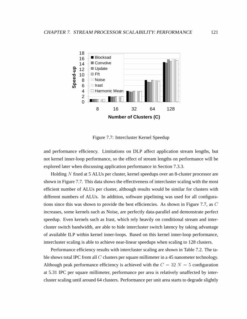
CHAPTER 7. STREAM PROCESSOR SCALABILITY: PERFORMANCE 121
02468
1012141618
8 16 32 64 128
Number of Clusters (C)
Sp
eed
-up
BlocksadConvolveUpdateFftNoiseIrastHarmonic Mean
Figure 7.7: Intercluster Kernel Speedup
and performance efficiency. Limitations on DLP affect application stream lengths, but
not kernel inner-loop performance, so the effect of stream lengths on performance will be
explored later when discussing application performance in Section 7.3.3.
Holding N fixed at 5 ALUs per cluster, kernel speedups over an 8-cluster processor are
shown in Figure 7.7. This data shows the effectiveness of intercluster scaling with the most
efficient number of ALUs per cluster, although results would be similar for clusters with
different numbers of ALUs. In addition, software pipelining was used for all configura-
tions since this was shown to provide the best efficiencies. As shown in Figure 7.7, as C
increases, some kernels such as Noise, are perfectly data-parallel and demonstrate perfect
speedup. Even kernels such as Irast, which rely heavily on conditional stream and inter-
cluster switch bandwidth, are able to hide intercluster switch latency by taking advantage
of available ILP within kernel inner-loops. Based on this kernel inner-loop performance,
intercluster scaling is able to achieve near-linear speedups when scaling to 128 clusters.
Performance efficiency results with intercluster scaling are shown in Table 7.2. The ta-
ble shows total IPC from all C clusters per square millimeter in a 45 nanometer technology.
Although peak performance efficiency is achieved with the C = 32 N = 5 configuration
at 5.31 IPC per square millimeter, performance per area is relatively unaffected by inter-
cluster scaling until around 64 clusters. Performance per unit area starts to degrade slightly

CHAPTER 7. STREAM PROCESSOR SCALABILITY: PERFORMANCE 122
Table 7.2: Intercluster Scaling Performance Efficiency
ClustersN 8 16 32 64 1282 5.23 5.16 5.18 5.05 5.005 5.29 5.29 5.31 5.22 4.95
10 4.39 4.47 4.20 4.08 3.8114 2.68 3.30 3.00 2.88 2.62
when scaling to 128 clusters. However, with performance per area of 4.95, the 640-ALU
C = 128 N = 5 processor is only 7% worse than the best C = 32 N = 5 processor.
Kernel Inner-Loop Performance Summary
The kernel inner-loop performance data presented above shows that given a fixed area bud-
get, without the use of software pipelining, it would be most efficient to only scale to 2
ALUs per cluster and then to utilize intercluster scaling to provide additional performance.
However, even with only 2 ALUs per cluster, the use of software pipelining was shown to
provide a 36% performance on inner-loop performance, meaning that this is a loop trans-
formation that provides significant performance gains for all cluster sizes. Once software
pipelining is used, intracluster scaling has near-linear speedups up to 10 ALUs on some ker-
nels, although was most efficient at 5 ALUs per cluster for most kernels. Therefore, with
the use of software pipelining, it would be most efficient to use intracluster scaling up to
5 ALUs per cluster and to use intercluster scaling, which provides near-linear speedups up
to 128 clusters on kernel inner loops, to further improve performance. An optimal perfor-
mance efficiency was found with 32 clusters and 5 ALUs per cluster, although performance
efficiency degraded by only 7% when scaling to 128 clusters.
Whereas software pipelining was shown to be a beneficial loop transformation for all
cluster sizes, the case for loop unrolling is less convincing. Loop unrolling shows the most
benefit for intracluster scaling for N > 5 and has a negligible impact for N <= 5. Even
though loop unrolling increases ILP for these larger clusters, the increase in ILP does not
overcome degradations in area efficiency and IPC per square millimeter gradually degrades

CHAPTER 7. STREAM PROCESSOR SCALABILITY: PERFORMANCE 123
from 5.33 to 4.50 when scaling from N = 5 to N = 10. However, loop unrolling and intr-
acluster scaling for the larger clusters is exploiting DLP which could have been exploited
with intercluster scaling, yet with much better performance efficiency. This data suggests
that intracluster scaling beyond N = 5 would not be as efficient from a performance effi-
ciency standpoint as intercluster scaling to up to 128 clusters.
7.3.2 Kernel Short Stream Effects
Kernel inner-loop performance speedups would reflect application speedups if stream lengths
scaled with machine size as the number of ALUs per stream processor are increased. If
stream lengths are held constant as machine size increases with intercluster scaling, then
the number of loop iterations executed per kernel invocation decreases, so the percentage
of runtime spent in kernel inner-loops decreases. If loop unrolling is used with intraclus-
ter scaling, the percentage of runtime spent in kernel inner-loops also decreases. In this
section, the effect that stream lengths have on kernel performance are measured.
Short stream effects were studied in some detail by Owens et al. [Owens et al., 2002;
Owens, 2002], and are similar to performance effects due to short vector lengths in vec-
tor processors [Asanovic, 1998]. With short streams, the number of inner loop iterations
executed per kernel call decreases, causing a larger fraction of execution time to be spent
in loop prologues and epilogues rather than in kernel inner loops. Furthermore, since soft-
ware pipelining is used extensively to optimize kernel inner-loop performance, a software
pipelining priming overhead is incurred with each kernel invocation.
The effect of stream length on kernel performance for a C = 8 processor on four media
processing kernels is shown in Figure 7.8. While inner-loop results from Section 7.3.1
showed the achievable IPC with infinitely long streams, meaning a negligible number of
cycles are spent outside inner loops, the results in Figure 7.8 show what happens to overall
kernel IPC when stream length is taken into account. For each kernel, IPC is shown as
stream length, L, is increased from 8 elements to 256 elements. Since C = 8, the number
of loop iterations executed per kernel call is given by L/8.
The None N2 results show average IPC without the use of software pipelining or loop
unrolling for N = 2. In this case, performance is relatively unaffected by stream length

CHAPTER 7. STREAM PROCESSOR SCALABILITY: PERFORMANCE 124
0.00
2.00
4.00
6.00
8.00
16 48 80 112 144 176 208 240
Co
nvo
lve
IPC
per
clu
ster
None_N2 SWP_N2 SWP_N5 SWP_N10 Unroll_N10 SWP2_N5
0.00
2.00
4.00
6.00
8.00
16 48 80 112 144 176 208 240
Up
dat
eIP
C p
er c
lust
er
0.00
2.00
4.00
6.00
8.00
16 48 80 112 144 176 208 240
FF
TIP
C p
er
clu
ster
0.00
2.00
4.00
6.00
8.00
16 48 80 112 144 176 208 240
Stream Length (Elements)
No
ise
IPC
per
clu
ster
Figure 7.8: Kernel Short Stream Effects

CHAPTER 7. STREAM PROCESSOR SCALABILITY: PERFORMANCE 125
since the loop prologues, bodies, and epilogues are all constrained by limits on true ILP and
inter-instruction dependencies within the kernels. Next, results with software pipelining for
three cluster sizes (N = 2, 5, and 10) are shown as SWP N2, SWP N5, and SWP N10. In
these cases, the kernel scheduler chose the number of software pipeline stages that would
minimize the inner loop length. In some of the kernels, up to 6 pipeline stages were used.
When software pipelining is used, IPC is much more dependent on stream length than in
the none N2 case, due to the overhead of software pipelining: given stream length L, a
kernel inner loop with S software pipeline stages executes L/C + (S − 1) times because
S − 1 iterations are required to prime a software pipelined loop. Finally, two other results
are shown: SWP2 N5 and Unroll N10. SWP2 N5 limits S to a maximum of two stages,
meaning kernel inner-loop length is greater than SWP N5, leading to better IPC for short
streams but worse IPC for long streams. Unroll N10 shows results with the use of software
pipelining and loop unrolling for N = 10. It performs worse than SWP N10 for the same
size streams for most kernels, with the exception being Update. Although Unroll N10
contains shorter inner loops, it executes half as many inner loop iterations as SWP N10,
leading to more software pipelining overhead.
Across the four kernels, for N = 2, the crossover point at which software pipelining
improves average kernel IPC is between 16 (Update) and 112 elements (Convolve). Al-
though not shown in the graph, with intracluster scaling, this crossover point shifts down:
for N = 5, software pipelining improves IPC across all four kernels for stream lengths of
32 elements or higher. This data suggests that our conclusions for N = 5 being the most
efficient cluster organization holds for reasonably sized streams since software pipelining
should be used for streams greater than 32 elements, and once software pipelining is used,
N = 5, was shown previously in Section 7.3.1 to be the most efficient cluster organization.
Further scaling to N = 10 and using loop unrolling to improve inner-loop IPC was shown
to be even less efficient when stream lengths are taken into account.
Although the results from Figure 7.8 are specific to a C = 8 processor, from this data,
the overall effect intercluster scaling has on kernel performance becomes more clear when
stream lengths are taken into account. During applications where dataset size limits stream
lengths, such as QRD, intercluster scaling with fixed dataset sizes would reduce stream
lengths. With streams significantly longer than the number of clusters, this would have

CHAPTER 7. STREAM PROCESSOR SCALABILITY: PERFORMANCE 126
a neglible effect on performance, but for short streams, this could reduce the achieved
speedup. For example, in the Update2 kernel (a key part of QRD), as shown in Figure 7.7,
an inner-looop speedup of 1.8x was achieved when scaling from 8 to 16 clusters. However,
when accounting for short stream effects, the overall kernel speedup would vary from 1.30x
to 1.72x for streams of length 32 elements and 512 elements, respectively.
Although short streams could limit speedup on some applications with intercluster scal-
ing with fixed dataset sizes, it is important to note that not all applications incur this perfor-
mance degradation with intercluster scaling. RENDER, for example, has enough available
DLP such that its stream lengths are limited by the capacity of the SRF, not the application
dataset. Therefore, its stream lengths are able to scale with the number of clusters and
the percentage of runtime in inner loops remains high. Applications such as these or with
large datasets (and therefore long streams) will have overall speedups similar to inner-loop
performance speedups.
7.3.3 Application Performance
In order to study the effect of intracluster and intercluster scaling on full applications with
fixed dataset sizes, the performance on RENDER, DEPTH, CONV, QRD, FFT1K, and
FFT4K were evaluated on a range of processor configurations. These results are shown in
Figure 7.9, as speedup over a C = 8 N = 5 processor. Sustained performance results in
GOPS for the C = 8 N = 5 processor, feasible in today’s technology, and the C = 128
N = 10 processor, the highest performing processor, are also annotated for each applica-
tion assuming a 1 GHz processor clock. All applications except FFT1K and FFT4K assume
data is initially in external memory. Since FFTs are typically part of a larger application,
their performance was measured with input data already in the SRF, and without simulating
the bit-reversed stores on the output data. The C = 128 N = 10 processor has the highest
performance with speedups over the C = 8 N = 5 configuration of 20.5x (311 GOPS) on
RENDER and 11.6x (328 GOPS) on DEPTH, and a harmonic mean of 10.4x across the six
applications.
Intracluster scaling of application performance is similar to kernel performance and is
mostly affected by the limited ILP in kernels and increased functional unit latencies. This

CHAPTER 7. STREAM PROCESSOR SCALABILITY: PERFORMANCE 127
128643216
8
Clusters
RENDER
DEPTH
CONV
QRD
FFT1K
FFT4K
HARMMEAN
ALUs per Cluster (N)
326GOPS
41.2GOPS
469GOPS
25.6GOPS
138GOPS
14.6GOPS
103GOPS
10.6GOPS
211GOPS
200GOPS
2 5 10 14
128643216
8
128643216
8
128643216
8
128643216
8
128643216
8
128643216
8
18.3GOPS
28.0GOPS
15.4GOPS
311GOPS
App
0.0 4.0 8.0 12.0 16.0 20.0 24.0
Speedup over C=8 N=5
Figure 7.9: Application Performance

CHAPTER 7. STREAM PROCESSOR SCALABILITY: PERFORMANCE 128
leads to little application-level speedup or even slow-downs in some cases when increasing
N from 10 to 14.
With intercluster scaling, speedups vary considerably depending on the application.
With large numbers of clusters and relatively small dataset sizes, some applications suffer
from short stream effects. In addition to the short stream effects exhibited during kernel ex-
ecution described above in Section 7.3.1, as stream lengths decrease relative to C, memory
latency and host processor bandwidth also begin to affect performance.
The effect short streams have on application performance with intercluster scaling is
evident from the breakdown of execution cycles in RENDER, DEPTH, and QRD, shown
in Figure 7.10. Execution cycles are grouped into four categories: kernel inner-loop cycles,
kernel non-inner-loop cycles, cycles when kernels are stalled waiting for SRF streams, and
cycles when kernels are not active because of memory or host bottlenecks. RENDER is
very data-parallel and contains stream lengths limited only by the total number of triangles
in a scene. Since this number stays large compared to C, the ratio of kernel inner-loop
iterations to kernel invocations stays high, and over 80% of runtime is devoted to processing
from kernel inner loops. As a result, RENDER scales very well to large numbers of clusters.
DEPTH also contains abundant data parallelism, however does not scale quite as well
as RENDER due to short stream effects and SIMD overheads. When streams contain only
pixels from one row of the input image, SIMD overheads (extra instructions executed in the
kernel inner loops per cluster) are small, but short stream effects cause a large percentage
of run-time to be spent in non-inner-loop kernel cycles, as seen in Figure 7.10 when going
from 8 to 16 clusters. For 32 clusters, the application is restructured so that each stream
contains pixels from 16 rows at a time, rather than the single row which was used for 8 and
16 clusters. The result is that over 95% of runtime is spent in the inner loops. However,
the operation count per inner loop is higher when clusters operate on streams that contain
pixels from more than one row in SIMD. Consequently, there is a sub-linear speedup from 8
to 32 clusters on DEPTH. The advantage of multiple-row DEPTH becomes apparent when
scaling to 64 and 128 clusters: short stream effects are avoided and large amounts of data
parallelism can be exploited.
With QRD, the matrix block update kernels scale well and if the datasets grew with
C, QRD performance would scale similarly. However, with a fixed-size dataset, the larger

CHAPTER 7. STREAM PROCESSOR SCALABILITY: PERFORMANCE 129
Inner Loop
Kernel Non-Inner Loop
SRF stalls
Clusters Idle(Memory or Host Stalls)
0%
10%
20%
30%
40%
50%
60%
70%
80%
90%
100%
8 16 32 64 128Clusters
QR
D
0%
10%
20%
30%
40%
50%
60%
70%
80%
90%
100%
8 16 32 64 128Clusters
DE
PT
H
0%
10%
20%
30%
40%
50%
60%
70%
80%
90%
100%
8 16 32 64 128Clusters
RE
ND
ER
Single-row streams Multi-row streams
Figure 7.10: Application Cycles with Intercluster Scaling (N=5)

CHAPTER 7. STREAM PROCESSOR SCALABILITY: PERFORMANCE 130
machines spend an increasing fraction of their runtime computing the orthogonal bases for
the decomposition, a step which scales poorly, therefore limiting speedup. In addition to
algorithmic inefficiencies leading to poor speedups, QRD with a fixed 256x256 dataset-size
also suffers from short stream effects, as can be seen in Figure 7.10, with a large percentage
of cycles spent outside of kernel inner-loops.
Direct evidence for performance degradation due to short stream effects is apparent
when comparing FFT4K to FFT1K in Figure 7.9. Although FFT4K has lower performance
than FFT1K at C = 8 N = 5 because its large working set requires spilling from the SRF
to memory, at C = 128 N = 10, the difference in raw performance between FFT4K and
FFT1K is due purely to stream length. On a C = 128 N = 10 processor, FFT4K sustains
211 GFLOPS, while FFT1K, containing shorter streams, only sustains 103 GFLOPS.
In summary, the advantages of intracluster scaling to exploit ILP and provide optimal
efficiency at 5 ALUs per cluster were apparent from kernel inner-loop performance. Similar
speedups in the intracluster scaling dimension were also achieved with full applications.
With intercluster scaling, kernel inner-loop performance results showed the ability to take
advantage of DLP in kernels with near-linear speedups up to 128 clusters on many kernels.
These kernel performance speedup numbers suggest how media application performance
would scale if dataset size scaled with machine size. However, with fixed dataset sizes,
limited DLP in some applications leads to short streams. Nevertheless, even with these
datasets, a 1280-ALU C = 128 N = 10 processor is able to sustain an average of 200
GOPS over six applications, a speedup of 10.4x over a 40-ALU C = 8 N = 5 processor.
7.3.4 Bandwidth Hierarchy Scaling
The tradeoffs between intracluster and intercluster scaling demonstrate the ability to ex-
ploit available ILP and DLP in media applications. However, not only must parallelism be
exploited, but a processor must exploit both the compute intensity and locality in media
applications in order to achieve high performance. With both intracluster and intercluster
scaling, the data bandwidth hierarchy has been scaled to exploit the available locality. This
is accomplished by increasing the LRF and SRF size and capacity as specified in Chapter 6.

CHAPTER 7. STREAM PROCESSOR SCALABILITY: PERFORMANCE 131
SRF BW
External Memory BW
LRF BW
0.1
1
10
100
1000
10000
8 16 32 64 128Clusters
GB
/s
0.1
1
10
100
1000
10000
8 16 32 64 128Clusters
GB
/s
0.1
1
10
100
1000
10000
8 16 32 64 128Clusters
GB
/s
RE
ND
ER
DE
PT
HQ
RD
Figure 7.11: Bandwidth Hierarchy with Intercluster Scaling (N=5)
CHAPTER 7. STREAM PROCESSOR SCALABILITY: PERFORMANCE 132
This scalable data bandwidth hierarchy in the stream architecture enables GFLOPs of arith-
metic performance to be sustained with modest off-chip memory bandwidth requirements.
The scalability of the data bandwidth hierarchy is shown on a logarithmic scale in Fig-
ure 7.11. With eight arithmetic clusters, between 380 and 565 GB/s of LRF bandwidth,
between 11 and 42 GB/s of SRF bandwidth, and between 0.33 and 2.87 GB/s of memory
bandwidth are necessary in the RENDER, DEPTH, and QRD applications. As intercluster
scaling is used to scale to 128 clusters, the LRF bandwidth demands grow by over an order
of magnitude to between 5.9 and 7.0 TB/s. However, since the SRF bandwidth and capacity
is also increased with the number of ALUs, the bandwidth hiearchy is able to handle this
increased LRF bandwidth. During RENDER, memory bandwidth is used only for input
and output operations, so its memory and SRF bandwidth scales as the same rate as the
LRFs. However, for DEPTH and QRD, with increased SRF capacity, additional locality
can be captured in the SRF, avoiding memory spills required in the smaller processors.
Since LRF and SRF bandwidth and capacity are increased appropriately with intraclus-
ter and intercluster scaling, the data bandwidth hierarchy is able to scale effectively to hun-
dreds of ALUs per stream processor. This scalablity allows for high sustained arithmetic
throughputs with hundreds of ALUs per stream processor with modest off-chip memory
systems. Furthermore, the scalability of the data bandwidth hierarchy means that over 95%
of data accesses in these future stream processors are made to the LRFs, not to the SRF or
external memory, leading to energy-efficient execution of these media applications.
7.4 Improving Intercluster and Intracluster Scalability
The results presented in Chapter 6 demonstrated the scalability of stream processors to
hundreds of arithmetic units with a less than 10% degradation in efficiency. For example,
a 640-ALU C = 128 N = 5 stream processor requires only 2% more area per ALU and
only 7% more energy per ALU operation than a 40-ALU C = 8 N = 5 stream proces-
sor. Furthermore, the results from this chapter demonstrated near-linear speedup on kernel
inner-loop performance when comparing a 640-ALU and 40-ALU processor. However, it
is worth considering whether additional microarchitectural optimizations in large stream
processors such as a 640-ALU processor could lead to area and energy efficiencies equal

CHAPTER 7. STREAM PROCESSOR SCALABILITY: PERFORMANCE 133
or better to a 40-ALU processor.
With slight modifications to the software tools and to microarchitecture used for intra-
cluster and intercluster scaling, area and energy efficiency could potentially be improved.
The two structures that stand out as not scaling as efficiently as the rest of the processor
and that could be improved are the intracluster and intercluster switches.
Several optimizations could be made to improve the intracluster switch. First, by adding
control bits to the intracluster switch, instead of broadcasting functional-unit outputs to all
LRF inputs, some bus segments could be disabled on a cycle-by-cycle basis in order to save
power. Second, area could be saved by using an explicitly scheduled sparse crossbar for
the intracluster switch. Currently, the kernel compiler requires a full crossbar connecting
the outputs of functional units to inputs of the LRFs in order to achieve high efficiencies in
kernel inner loops. However, with some kernel compiler improvements, a sparse crossbar
would reduce the area of the switch as the number of ALUs per cluster increased and
would have the potential to increase the number of ALUs per cluster that achieved optimal
performance efficiencies on a range of ALUs. Although most kernels would have to convert
DLP to ILP with loop unrolling to have performance scale effectively beyond 5 ALUs per
cluster, some kernels have enough ILP to take advantage of the additional parallelism that
could be enabled with an efficient intracluster switch.
The switch is the limiting structure in intercluster scaling as well. A sparse crossbar for
the intercluster switch could further improve area and energy efficiency for larger numbers
of clusters. In the intercluster case, the communication across the switch is input from the
programmer and is based on communication patterns required in the applications.
Just as locality could be exploited by the VLIW compiler in the intracluster switch, if
locality exists in intercluster communication patterns, a switch that could exploit this to
improve area and energy efficiency. The available locality in intercluster communications
was studied by looking at the 13 permutations from the kernel inner-loops in DEPTH,
FFT, and QRD on 64-cluster machines. An 8x8 cluster grid floorplan was assumed, where
clusters 0 through 7 are in column 0, clusters 8 through 15 are in column 1, and so on up
to clusters 56 to 63 in column 7. Given this floorplan, the histogram shown in Figure 7.12
demonstrates the locality in these permutation patterns. Since 13 permutations are studied,
832 total communications are grouped into 15 categories based on the number of hops

CHAPTER 7. STREAM PROCESSOR SCALABILITY: PERFORMANCE 134
Intercluster Permutation Histogramfor 64 Clusters
0
20
40
60
80
100
120
140
160
0 1 2 3 4 5 6 7 8 9 10 11 12 13 14
Number of Hops
Nu
mb
er o
f C
om
mu
nic
atio
ns
Figure 7.12: Intercluster Switch Locality with 8x8 Cluster Grid Floorplan
which must be traveled between clusters. Note that in an 8x8 grid, the maximum number
of hops is 14. This histogram shows that indeed some locality exists as the most common
case is 4 hops and only 6.5% of communications require greater than 8 hops.
Future research could explore intercluster switch topologies that could provide better
area and energy efficiency by exploiting the locality between clusters during communica-
tions. One example of a switch topology for an 8x8 cluster grid that exploits this locality
is shown in Figure 7.13. Similar to the full crossbar shown in Figure 6.1, in this figure,
each cluster broadcasts its output across its row bus and reads an input onto its column bus.
However, in this topology, row and column buses span only 2 clusters in each direction,
meaning communications are limited to four hops maximum. Permutations with maxi-
mum hop counts greater than 4 would require more than one communication to route the
data succesfully, leading to more required switch bandwidth in some kernels. However, this
topology has an area-efficiency advantage over a full crossbar because it only requires five
buses per column and per row, whereas a full crossbar requires eight buses per column and

CHAPTER 7. STREAM PROCESSOR SCALABILITY: PERFORMANCE 135
1680 403224 5648
1791 413325 5749
18102 423426 5850
19113 433527 5951
20124 443628 6052
21135 453729 6153
22146 463830 6254
23157 473931 6355
Figure 7.13: Limited-Connectivity Inercluster Switch for 8x8 Cluster Floorplan

CHAPTER 7. STREAM PROCESSOR SCALABILITY: PERFORMANCE 136
per row. Future research could explore the tradeoff between performance and efficiency for
this and other switch topologies.
7.5 Scalability Summary
As technology enables more ALUs to fit on a single chip, architectures must efficiently
utilize bandwidth in order to achieve large performance gains. In this chapter, two scaling
techniques for stream processors that enable large performance gains on media processing
applications in future VLSI technologies were presented. Intracluster scaling was shown
to be effective from a performance and cost standpoint up to 10 ALUs per cluster, although
was most efficient at 5 ALUs per cluster. This optimal efficiency at 5 ALUs per cluster is
derived from amortizing fixed cluster costs such as streambuffers, the intercluster switch
ports, and the scratchpad over more ALUs. Meanwhile, near-linear speedups are achievable
up to 5 ALUs with the use of software pipelining. Beyond 5 ALUs, the ILP available from
software pipelining trails off and the cost of the intracluster switch and additional required
intercluster switch port hurts efficiency. Intercluster scaling was shown to be effective up to
128 clusters, with only a slight decrease in area and energy efficiency. In addition, a variety
of media applications were shown to have significant parallelism and no prohibitive limits
on inherent stream lengths in the application, thereby enabling speedups of up to 27.4x and
10.0x when comparing a 1280-ALU to a 40-ALU stream processor on a harmonic mean of
kernels and applications.

Chapter 8
Conclusions
In this dissertation, stream processors were shown to achieve performance rates and per-
formance efficiencies significantly higher than other programmable processors on media
applications, and approaching the efficiencies of fixed-function processors. The Imagine
architecture, the first VLSI implementation of a stream processor, is able to achieve high
performance and efficiencies by exploiting large amounts of parallelism, by exploiting lo-
cality to effectively manage data bandwidth, and by the use of area- and energy-efficient
register organization.
Furthermore, the architectural concepts and performance measurements validated with
the Imagine stream processor can be extended to future technologies using the intercluster
and intracluster scaling techniques presented in this dissertation. The analysis presented
in this work demonstrates the scalability of stream processors to thousands of arithmetic
units in future VLSI technologies with comparable performance efficiencies to stream pro-
cessors containing tens of arithmetic units. These future stream processors will be capable
of sustaining hundreds of billions of arithmetic operations per second while maintaining
high performance efficiencies, enabling a large set of new and existing real-time media
applications in a wide variety of mobile, desktop, and server systems, while retaining the
advantages of programmability.
137
CHAPTER 8. CONCLUSIONS 138
8.1 Future Work
The work described here leads to a number of other interesting areas of future research:
Imagine System
Although this dissertation presents the design and implementation of the Imagine processor,
one important area of future work is in system design for the Imagine stream processor. The
experimental measurements described in Chapter 5 were obtained with a PCI board con-
taining two Imagine processors, a host processor, glue-logic FPGAs, and DRAM chips. At
the time this dissertation was submitted, this board was not able to run all available media
applications at real-time due to host-processor and glue-logic limitations (not because of
host interface bandwidth limitations on the Imagine processor). Future work is underway to
redesign a board which eliminates these limitations enabling real-time execution of a larger
range of media applications. Another ongoing area of research is multiprocessor systems
using the Imagine network interface. This research would lead to a number of key insights
into performance, software tools, and host processor requirements in these multi-Imagine
systems.
Applications
In this dissertation, the evaluation of stream processing was restricted to media processing
requirements with today’s workloads and datasets. However, as stream processors scale
to Teraops of performance with high performance efficiencies, such processors will pro-
vide the potential for running more complex media processing algorithms and much larger
datasets at real-time rates. For example, in computer graphics, polygon rendering with
higher scene complexity and screen resolutions would require larger datasets and more
performance to achieve real-time rates. Furthermore, raytracing and image-based rendering
techniques have been emerging as alternative applications for computer graphics also re-
quiring higher performance than polygon rendering. These trends suggest that as available
media processor performance increases, media applications and their datasets will evolve
to take advantage of this available performance while sustaining real-time rates. Therefore,
an important area of future work would be to explore how media processors can scale in a

CHAPTER 8. CONCLUSIONS 139
way to provide the types of performance rates required for future media applications, rather
than today’s applications.
Another area of future work for applications of stream processors is in broadening the
application domains. Recent work has started to explore the effectiveness of stream pro-
cessing to both scientific workloads [Dally et al., 2001] and signal processing for wireless
communications [Rajagopal et al., 2002]. Such application domains share many of the
same application characteristics as media applications, but differ slightly, meaning that en-
hancements and optimizations to the stream processor architecture and microarchitecture
could be made to improve performance and VLSI efficiency on these applications.
VLSI Efficient Stream Processing
The VLSI efficiency of stream processing stems from the stream register organization that
allows for efficient use of parallelism and locality and media applications. One area of fu-
ture work would be to explore enhancements to this register organization that could further
improve the VLSI efficiency of stream processors. Such enhancements were briefly dis-
cussed in Chapter 7 with studies into non-fully-interconnected intercluster switches. How-
ever, other possibilities for improvement include a non-fully-interconnected intracluster
switch and slightly modified local register file structures. For example, rather than using
two dual-ported register files per arithmetic unit, other structures such as one multi-ported
register file per arithmetic unit could be explored. Although such a structure would require
more interconnectivity in the read and write ports, such a design might be more efficient if
this interconnect could be overlapped with memory cells and other transistors in this regis-
ter file design. This and other improvements to the register organization could be explored
to achieve small improvements in the VLSI efficiency of stream processing.
Scalability
A final area of future work involves scalability to large numbers of arithmetic units per
chip in future technologies. In this dissertation, the two techniques of intracluster and
intercluster scaling were presented and evaluated. These two dimensions of scaling are
able to exploit instruction-level and data-level parallelism respectively. However, a third

CHAPTER 8. CONCLUSIONS 140
dimension of scaling is also possible, in the task-level (or thread-level) dimension. This
scaling technique would involve either multiple kernel execution units (microcontroller
with some number of clusters) connected to a single stream register file or multiple stream
processor cores on a single chip. In these architectures, multiple kernels could be executing
simultaneously, thereby exploiting task-level parallelism. As software tools for exploiting
these scaling techniques mature, the performance and cost advantages of exploiting task-
level parallelism could be explored and compared to intracluster and intercluster scaling.
In summary, the work presented in this thesis describes the first VLSI implementation
of a stream processor and describes scaling techniques that show the viability of stream
processing for many years to come. This is an area of research that is just beginning and
will lead to new and exciting results in the areas of real-time media processing and power-
efficient computer architecture.

Bibliography
[Agarwal et al., 2000] Vikas Agarwal, M.S. Hrishikesh, Stephen W. Keckler, and Doug
Burger. Clock rate versus IPC: The end of the road for conventional microarchitectures.
In 27th Annual International Symposium on Computer Architecture, pages 248–259,
June 2000.
[Agarwala et al., 2002] S. Agarwala, P. Koeppen, T. Anderson, A. Hill, M. Ales,
R. Damodaran, L. Nardini, P. Wiley, S. Mullinnix, J. Leach, A. Lell, M. Gill, J. Gol-
ston, D. Hoyle, A. Rajagopal, A. Chachad, M. Agarwala, R. Castille, N. Common,
J. Apostol, H. Mahmood, M. Krishnan, D. Bui, Q. An, P. Groves, L. Nguyen, N. Na-
garaj, and R. Simar. A 600 MHz VLIW DSP. In 2002 International Solid-State Circuits
Conference Digest of Technical Papers, pages 56–57, 2002.
[Asanovic, 1998] Krste Asanovic. Vector Microprocessors. PhD thesis, University of Cal-
ifornia at Berkeley, 1998.
[Bhattacharyya et al., 1996] Shuvra S. Bhattacharyya, Praveen K. Murthy, and Edward A.
Lee. Software Synthesis from Dataflow Graphs. Kluwer Academic Press, Norwell, MA,
1996.
[Booth, 1951] A. D. Booth. A signed binary multiplication technique. Quarterly Journal
of Mechanics and Applied Mathematics, 4:236–240, 1951.
[Bove and Watlington, 1995] V. Michael Bove and John A. Watlington. Cheops: A re-
configurable data-flow system for video processing. IEEE Transactions on Circuits and
Systems for Video Technology, 3(2):140–149, April 1995.
141

BIBLIOGRAPHY 142
[Brooks and Shearer, 2000] Thomas Brooks and Findlay Shearer. Communications core
meets 3G wireless handset challenges. Wireless Systems Design, pages 51–56, October
2000.
[Burd and Brodersen, 1995] Thomas D. Burd and Robert W. Brodersen. Energy-efficient
cmos microprocessor design. In 28th Hawaii International Conference on System Sci-
ences, pages 288–297, January 1995.
[Caspi et al., 2001] Eylon Caspi, Andre Dehon, and John Wawrzynek. A streaming multi-
threaded model. In Proceedings of the Third Workshop on Media and Stream Processors,
pages 21–28, Austin, TX, Dec 2001.
[Chandrakasan et al., 1994] Anantha Chandrakasan, Samuel Sheng, and Robert W.
Brodersen. Low power CMOS digital design. In IEEE Journal of Solid State Circuits,
pages 473–484, October 1994.
[Chang, 1998] Andrew Chang. VLSI datapath choices: Cell-based versus full-custom.
Master’s thesis, MIT, 1998.
[Chen et al., 1997] Kai Chen, Chenming Hu, Peng Fang, Min Ren Lin, and Donald L.
Wollesen. Predicting CMOS speed with gate oxide and voltage scaling and interconnect
loading effects. IEEE Transactions on Electron Devices, 44(11):1951–1957, November
1997.
[Chen, 1999] David Chen. Apollo II adds power capabilities, speeds VDSM place and
route. Electronics Journal, page 25, July 1999.
[Chinnery and Keutzer, 2000] D. Chinnery and K. Keutzer. Closing the gap between ASIC
and custom: An ASIC perspective. In Proceedings of 37th Design Automation Confer-
ence, pages 637–641, June 2000.
[Chinnery and Keutzer, 2002] D. Chinnery and K. Keutzer. Closing the Gap Between
ASIC and Custom: Tools and Techniques for High-Performance ASIC Design. Kluwer
Academic Publishers, May 2002.

BIBLIOGRAPHY 143
[Chowdhary et al., 1999] A. Chowdhary, S. Kale, P.K. Saripella, N.K. Sehgal, and R.K.
Gupta. Extraction of functional regularity in datapath circuits. IEEE Transactions on
Computer-Aided Design of Integrated Circuits and Systems, 18(9):1279–1296, Septem-
ber 1999.
[Clark et al., 2001] Lawrence T. Clark, Eric J. Hoffman, Jay Miller, Manish Biyani, Yuyun
Liao, Stephen Strazdus, Michael Morrow, Kimberley E. Velarde, and Mark A. Yarch. An
embedded 32-b microprocessor core for low-power and high-performance applications.
In IEEE Journal of Solid State Circuits, pages 1599–1608, November 2001.
[Coonen, 1980] Jerome T. Coonen. An implementation guide to a proposed standard for
floating-point arithmetic. Computer, 13(1):68–79, January 1980.
[Cradle, 2003] Cradle technologies white paper: The software scalable system on a chip
(3SOC) architecture, 2003.
[Dally and Chang, 2000] William J. Dally and Andrew Chang. The role of custom designs
in ASIC chips. In Proceedings of 37th Design Automation Conference, pages 643–647,
June 2000.
[Dally and Poulton, 1998] William J. Dally and John Poulton. Digital Systems Engineer-
ing, pages 12–22. Cambridge University Press, 1998.
[Dally et al., 2001] William J. Dally, Pat Hanrahan, and Ron Fedkiw. A streaming super-
computer. Stanford Computer Systems Laboratory White Paper, September 2001.
[Dally, 1992] William J. Dally. Virtual channel flow control. IEEE Transactions on Par-
allel and Distributed Systems, pages 194–205, March 1992.
[Davis et al., 2001] W. Rhett Davis, Ning Zhang, Kevin Camera, Fred Chen, Dejan
Markovic, Nathan Chan, Borivoje Nikolic, and Robert W. Brodersen. A design envi-
ronment for high throughput, low power dedicated signal processing systems. In IEEE
2001 Conference on Custom Integrated Circuits, pages 545–548, May 2001.
[de Kock et al., 2000] E.A. de Kock, G. Essink, W.J.M. Smits, R. van der Wolf, J.-Y.
Brunei, W.M. Kruijtzer, P. Lieverse, and K.A. Vissers. YAPI: Application modeling

BIBLIOGRAPHY 144
for signal processing systems. In Proceedings of 37th Design Automation Conference,
pages 402–405, June 2000.
[Gieseke et al., 1997] Bruce A. Gieseke, Randy L. Allmon, Daniel W. Bailey, Bradley J.
Benschneider, Sharon M. Britton, John D. Clouser, Harry R. Fair III, James A. Far-
rell, Michael K. Gowan, Christopher L. Houghton, James B. Keller, Thomas H. Lee,
Daniel L. Leibholz, Susan C. Lowell, Mark D. Matson, Richard J. Matthew, Victor
Peng, Michael D. Quinn, Donald A. Priore, Michael J. Smith, and Kathryn E. Wilcox.
A 600 MHz superscalar RISC microprocessor with out-of-order execution. In 1997 In-
ternational Solid-State Circuits Conference Digest of Technical Papers, pages 176–177,
1997.
[Gokhale et al., 2000] Maya Gokhale, Jan Stone, Jeff Arnold, and Mirek Kalinowski.
Stream-oriented FPGA computing in the Streams-C high level language. In 2000 IEEE
Symposium on Field-Programmable Custom Computing Machines, pages 49–56, 2000.
[Goldberg, 2002] David Goldberg. Computer Arithmetic, Appendix H of C̈omputer Archi-
tecture: A Quantitative Approachb̈y John Hennessy and David Patterson, Third Edition,
page Appendix H. Morgan Kaufmann, 2002.
[Goldovsky et al., 2000] Alexander Goldovsky, Bimal Patel, Michael Schulte, Ravi Ko-
lagotla, Hosahalli Srinivas, and Geoffrey Burns. Design and implementation of a 16
by 16 low-power two’s complement multiplier. In IEEE International Symposium on
Circuits and Systems., volume 5, pages 345–348, May 2000.
[Golston, 2000] Jeremiah Golston. TMS320C64x architecture extensions boost perfor-
mance for broadband communications and imaging. In Hotchips 12, August 2000.
[Gordon et al., 2002] Michael I. Gordon, William Thies, Michal Karczmarek, Jasper Lin,
Ali S. Meli, Andrew A. Lamb, Chris Leger, Jeremy Wong, Henry Hoffmann, David
Maze, and Saman Amarasinghe. A stream compiler for communication-exposed archi-
tectures. In Proceedings of the Tenth International Conference on Architectural Support
for Programming Languages and Operating Systems, pages 82–92, October 2002.
BIBLIOGRAPHY 145
[Green, 2000] Peter K. Green. A GHz IA-32 architecture microprocessor implemented on
0.18 µm technology with aluminum interconnect. In 2000 IEEE International Solid-
State Circuits Conference Digest of Technical Papers, pages 98–99,449, February 2000.
[Ho et al., 2001] Ron Ho, Ken Mai, and Mark Horowitz. The future of wires. Proceedings
of the IEEE, April 2001.
[Horowitz et al., 1994] Mark Horowitz, Thomas Indermaur, and Ricardo Gonzalez. Low-
power digital design. In Symposium on Low Power Electronics, pages 102–103, October
1994.
[Huang and Ercegovac, 2002] Zhijun Huang and Milos D. Ercegovac. Two dimensional
signal gating for low-power array multiplier design. In IEEE International Symposium
on Circuits and Systems., volume 1, pages I–489–I–492, 2002.
[Intel, 2002] Intel Corp. Intel Pentium 4 Processor with 512-KB L2 Cache on 0.13 Micron
Process at 2 GHz - 3.06 GHz, with Support for Hyper-Threading Technology at 3.06
Ghz, document number: 298643-005 edition, November 2002.
[Janssen and Corporaal, 1995] Johan Janssen and Henk Corporaal. Partitioned register
files for TTAs. In Proceedings of the 28th Annual IEEE/ACM International Symposium
on Microarchitecture, pages 303–312, November 1995.
[Jouppi, 1990] Norman P. Jouppi. Improving direct-mapped cache performance by the
addition of a small fully-associative cache and prefetch buffers. In Proceedings of the
International Symposium on Computer Architecture, pages 364–373, May 1990.
[Kanade et al., 1996] Takeo Kanade, Atsushi Yoshida, Kazuo Oda, Hiroshi Kano, and
Masaya Tanaka. A stereo machine for video-rate dense depth mapping and its new
applications. In Proceedings of the 15th Computer Vision and Pattern Recognition Con-
ference, pages 196–202, San Francisco, CA, June 18–20, 1996.
[Kapadia et al., 1995] Hema Kapadia, Katayoun Falakshahi, and Mark Horowitz. Array-
of-arrays architecture for floating point multiplication. In Advanced Research in VLSI,
pages 150–157, March 1995.

BIBLIOGRAPHY 146
[Kapasi et al., 2000] Ujval J. Kapasi, William J. Dally, Scott Rixner, Peter R. Mattson,
John D. Owens, and Brucek Khailany. Efficient conditional operations for data-parallel
architectures. In Proceedings of the 33rd Annual IEEE/ACM International Symposium
on Microarchitecture, pages 159–170, December 2000.
[Kapasi et al., 2001] Ujval J. Kapasi, Peter Mattson, William J. Dally, John D. Owens, and
Brian Towles. Stream scheduling. In Proceedings of the Third Workshop on Media and
Stream Processors, pages 101–106, Austin, TX, Dec 2001.
[Khailany et al., 2001] Brucek Khailany, William J. Dally, Scott Rixner, Ujval J. Kapasi,
Peter Mattson, Jin Namkoong, John D. Owens, Brian Towles, and Andrew Chang. Imag-
ine: Media processing with streams. IEEE Micro, pages 35–46, Mar/Apr 2001.
[Khailany et al., 2002] Brucek Khailany, William J. Dally, Andrew Chang, Ujval J. Ka-
pasi, Jinyung Namkoong, and Brian Towles. VLSI design and verification of the Imagine
processor. In Proceedings of the IEEE International Conference on Computer Design,
pages 289–296, September 2002.
[Khailany et al., 2003] Brucek Khailany, William J. Dally, Scott Rixner, Ujval J. Kapasi,
John D. Owens, and Brian Towles. Exploring the VLSI scalability of stream processors.
In Proceedings of the Ninth International Symposium on High Performance Computer
Architecture, pages 153–164, February 2003.
[KleinOsowski et al., 2000] AJ KleinOsowski, John Flynn, Nancy Meares, and David J.
Lilja. Adapting the SPEC 2000 benchmark suite for simulation-based computer archi-
tecture research. In Workshop on Workload Characterization, International Conference
on Computer Design (ICCD), September 2000.
[Kohn and Fu, 1989] Leslie Kohn and Sai-Wai Fu. A 1,000,000 transistor microprocessor.
In 1989 International Solid-State Circuits Conference Digest of Technical Papers, pages
54–55, 290, 1989.

BIBLIOGRAPHY 147
[Kozyrakis and Patterson, 2002] Christos Kozyrakis and David Patterson. Vector vs. su-
perscalar and VLIW architectures for embedded multimedia benchmarks. In Proceed-
ings of the 35th Annual IEEE/ACM International Symposium on Microarchitecture,
pages 283–293, November 2002.
[Kozyrakis and Patterson, 2003] Christos Kozyrakis and David Patterson. Overcoming the
limitations of conventional vector processors. In 30th Annual International Symposium
on Computer Architecture, June 2003.
[Kozyrakis, 2002] Christoforos Kozyrakis. Scalable Vector Media-processors for Embed-
ded Systems. PhD thesis, University of California at Berkeley, 2002.
[Kutzschebauch and Stok, 2000] T. Kutzschebauch and L. Stok. Regularity driven logic
synthesis. In Proceedings of the International Conference on Computer Aided Design,
pages 439–446, November 2000.
[Lee and Parks, 1995] Edward A. Lee and Thomas M. Parks. Dataflow process networks.
Proceedings of the IEEE, 83(5), May 1995.
[Lee and Stoodley, 1998] Corinna G. Lee and Mark G. Stoodley. Simple vector micro-
processors for multimedia applications. In Proceedings of the 31st Annual IEEE/ACM
International Symposium on Microarchitecture, pages 25–36, December 1998.
[Lee, 1996] Ruby B. Lee. Subword parallelism with MAX-2. IEEE Micro, pages 51–59,
August 1996.
[Mai et al., 2000] Ken Mai, Tim Paaske, Nuwan Jayasena, Ron Ho, William J. Dally, and
Mark Horowitz. Smart memories: A modular reconfigurable architecture. In 27th An-
nual International Symposium on Computer Architecture, pages 161–171, June 2000.
[Malachowsky, 2002] Chris Malachowsky. When 10M gates just isn’t enough....the GPU
challenge. In Proceedings of 39th Design Automation Conference, June 2002.

BIBLIOGRAPHY 148
[Mattson et al., 2000] Peter Mattson, William J. Dally, Scott Rixner, Ujval J. Kapasi, and
John D. Owens. Communication scheduling. In Proceedings of the International Con-
ference on Architectural Support for Programming Languages and Operating Systems,
pages 82–92, November 2000.
[Mattson, 2001] Peter Mattson. A Programming System for the Imagine Media Processor.
PhD thesis, Stanford University, 2001.
[Montrym and Moreton, 2002] John Montrym and Henry Moreton. Nvidia GeForce4. In
Hotchips 14, August 2002.
[Nagamatsu et al., 1990] Masato Nagamatsu, Shigeru Tanaka, Junji Mori, Katsusi Hirano,
Tatsuo Noguchi, and Kazuhisa Hatanaka. A 15-ns 32x32-b CMOS multiplier with an
improved parallel structure. In IEEE Journal of Solid State Circuits, pages 494–497,
April 1990.
[Nickolls et al., 2002] John Nickolls, L. J. Madar III, Scott Johnson, Viresh Rustagi, Ken
Unger, and Mustafiz Choudhury. Broadcom Calisto: A multi-channel multi-service
communications platform. In Hotchips 14, August 2002.
[Nijssen and van Eijk, 1997] Raymond X.T. Nijssen and C.A.J. van Eijk. Regular layout
generation of logically optimized datapaths. In Proceedings of the International Sym-
posium on Physical Design, pages 42–47, 1997.
[Ohashi et al., 2002] Masahiro Ohashi, T. Hashimoto, S.I. Kuromaru, M. Matsuo, T. Mori-
iwa, M. Hamada, Y. Sugisawa, M. Arita, H. Tomita, M. Hoshino, H. Miyajima, T. Naka-
mura, K.I. Ishida, T. Kimura, Y. Kohashi, T. Kondo, A. Inoue, H. Fujimoto, K. Watada,
T. Fukunaga, T. Nishi, H. Ito, and J. Michiyama. A 27 MHz 11.1 mW MPEG-4 video
decoder LSI for mobile application. In 2002 IEEE International Solid-State Circuits
Conference Digest of Technical Papers, pages 366–367, February 2002.
[Olofsson and Lange, 2002] Andreas Olofsson and Fredy Lange. A 4.32GOPS 1W
general-purpose DSP with an enhanced instruction set for wireless communication. In
2002 International Solid-State Circuits Conference Digest of Technical Papers, pages
54–55,443, 2002.

BIBLIOGRAPHY 149
[Owens et al., 2002] John D. Owens, Scott Rixner, Ujval J. Kapasi, Peter Mattson, Ben
Serebrin, and William J. Dally. Media processing applications on the Imagine stream
processor. In Proceedings of the IEEE International Conference on Computer Design,
pages 295–302, September 2002.
[Owens, 2002] John Owens. Computer Graphics on a Stream Architecture. PhD thesis,
Stanford University, 2002.
[Peleg and Weiser, 1996] Alex Peleg and Uri Weiser. MMX technology extension to the
Intel architecture. IEEE Micro, pages 42–50, August 1996.
[Phillip, 1998] Mike Phillip. Altivec: A second generation SIMD microprocessor archi-
tecture. In Hotchips 10, August 1998.
[Rajagopal et al., 2002] Sridhar Rajagopal, Scott Rixner, and Joseph R. Cavallaro. A pro-
grammable baseband processor design for software defined radios. In 45th IEEE In-
ternational Midwest Symposium on Circuits and Systems, volume 3, pages 413–416,
August 2002.
[Rambus, 2001] Rambus. 512/576 Mb 1066 MHz RDRAM Datasheet, DL-0117-030 ver-
sion 0.3, 3.6MB, 11/01 edition, 2001.
[Ranganathan et al., 1999] Parthasarathy Ranganathan, Sarita Adve, and Norman P.
Jouppi. Performance of image and video processing with general-purpose processors
and media ISA extensions. In Proceedings of the 26th International Symposium on
Computer Architecture, pages 124–135, May 1999.
[Rathnam and Slavenburg, 1996] Selliah Rathnam and Gerrit A. Slavenburg. An architec-
tural overview of the programmable media processor, TM-1. In Proceedings of COMP-
CON, pages 319–326, February 1996.
[Rau et al., 1982] B. Ramakrishna Rau, Christopher D. Glaeser, and Raymond L. Picard.
Efficient code generation for horizontal architectures: Compiler techniques and architec-
tural support. In Proceedings of the International Symposium on Computer Architecture,
pages 131–139, April 1982.

BIBLIOGRAPHY 150
[Rau et al., 1989] B. Ramakrishna Rau, David W. L. Yen, Wei Yen, and Ross A. Towle.
The Cydra 5 departmental supercomputer: Design philosophies, decisions, and trade-
offs. Computer, pages 12–35, January 1989.
[Rixner et al., 1998] Scott Rixner, William J. Dally, Ujval J. Kapasi, Brucek Khailany,
Abelardo Lopez-Lagunas, Peter Mattson, and John D. Owens. A bandwidth-efficient
architecture for media processing. In Proceedings of the 31st Annual IEEE/ACM Inter-
national Symposium on Microarchitecture, pages 3–13, November 1998.
[Rixner et al., 2000a] Scott Rixner, William J. Dally, Ujval J. Kapasi, Peter R. Mattson,
and John D. Owens. Memory access scheduling. In 27th Annual International Sympo-
sium on Computer Architecture, pages 128–138, June 2000.
[Rixner et al., 2000b] Scott Rixner, William J. Dally, Brucek Khailany, Peter Mattson, Uj-
val J. Kapasi, and John D. Owens. Register organization for media processing. In
Proceedings of the Sixth International Symposium on High Performance Computer Ar-
chitecture, pages 375–387, January 2000.
[Rixner, 2001] Scott Rixner. Stream Processor Architecture. Kluwer Academic Publish-
ers, Boston, MA, 2001.
[Russell, 1978] Richard M. Russell. The Cray-1 computer system. Communications of the
ACM, 21(1):63–72, January 1978.
[Sager et al., 2001] David Sager, Glenn Hinton, Michael Upton, Terry Chappell,
Thomas D. Fletcher, Samie Samaan, and Robert Murray. A 0.18 µm CMOS IA32
microprocessor with a 4GHz integer execution unit. In 2001 International Solid-State
Circuits Conference Digest of Technical Papers, pages 324–325, 2001.
[Santoro et al., 1989] Mark R. Santoro, Gary Bewick, and Mark Horowitz. Rounding al-
gorithms for IEEE multipliers. In Proceedings of the 9th Symposium on Computer Arith-
metic, pages 176–183, September 1989.
[SIA, 2001] Semiconductor industry association: The international technology roadmap
for semiconductors, 2001.

BIBLIOGRAPHY 151
[Sibyte, 2000] Sibyte. SB-1250 Product Data Sheet, rev 0.2 edition, October 2000.
[Simulink, 2002] Mathworks. Simulink: Model-Based and System-Based Design (Using
Simulink), version 5 edition, 2002.
[Synopsys, 2000a] Synopsys. Design Compiler User Guide, 2000.11 edition, 2000.
[Synopsys, 2000b] Synopsys. Physical Compiler User Guide, 2000.11 edition, 2000.
[Thakkar and Huff, 1999] Shreekant Thakkar and Tom Huff. The internet streaming SIMD
extensions. Intel Technology Journal, Q2, 1999.
[Thompson et al., 2001] S. Thompson, M. Alavi, R. Arghavani, A. Brand, R. Bigwood,
J. Brandenburg, B. Crew, V. Dubin, M. Hussein, P. Jacob, C. Kenyon, E. Lee, B. Mcin-
tyre, Z. Ma, P. Moon, P. Nguyen, M. Prince, R. Schweinfurth, S. Sivakumar, P. Smith,
M. Stettler, S. Tyagi, M. Wei, J. Xu, S. Yang, and M. Bohr. An enhanced 130 nm gener-
ation logic technology featuring 60 nm transistors optimized for high performance and
low power at 0.7 - 1.4 V. In 2001 International Electron Devices Meeting, pages 11.6.1
–11.6.4, 2001.
[TI, 2003] Texas Instruments. TMS320C6713, TMS320C6713 Floating-Point Digital Sig-
nal Processors, sprs186c - december 2001 - revised march 2003 edition, March 2003.
[Tremblay et al., 1996] Marc Tremblay, J. Michael O’Connor, Venkatesh Narayanan, and
Liang He. VIS speeds new media processing. IEEE Micro, pages 10–20, August 1996.
[Tyagi et al., 2000] S. Tyagi, M. Alavi, R. Bigwood, T. Bramblett, J. Brandenburg,
W. Chen, B. Crew, M. Hussein, P. Jacob, C. Kenyon, C. Lo, B. McIntyre, Z. Ma,
P. Moon, P. Nguyen, L. Rumaner, R. Schweinfurth, S. Sivakumar, M. Stettler, S. Thomp-
son, B. Tufts, J. Xu, S. Yang, and M. Bohr. A 130 nm generation logic technology fea-
turing 70 nm transistors, dual Vt transistors and 6 layers of Cu interconnects. In 2000
International Electron Devices Meeting, pages 567–570, 2000.
[Waingold et al., 1997] Elliot Waingold, Michael Taylor, Devabhaktuni Srikrishna, Vivek
Sarkar, Walter Lee, Victor Lee, Jang Kim, Matthew Frank, Peter Finch, Rajeev Barua,

BIBLIOGRAPHY 152
Jonathan Babb, Saman Amarasinghe, , and Anant Agarwal. Bearing it all to software:
RAW machines. Computer, pages 86–93, September 1997.
[Wawrzynek et al., 1996] John Wawrzynek, Krste Asanovic, Brian Kingsbury, David
Johnson, James Beck, and David Morgan. Spert II: A vector microprocessor system.
Computer, pages 79–86, March 1996.
[Weste and Eshraghian, 1993] Neil H. E. Weste and Kamran Eshraghian. Principles of
CMOS VLSI Design: A Systems Perspective, Second Edition, pages 560–563. Addison-
WesleyPublishing Company, 1993.