Embed Size (px)
Citation preview
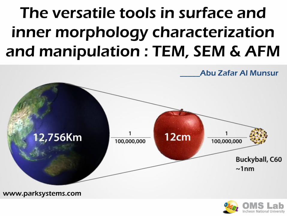
The versatile tools in surface and
inner morphology characterization
and manipulation : TEM, SEM & AFM
_____Abu Zafar Al Munsur
www.parksystems.com
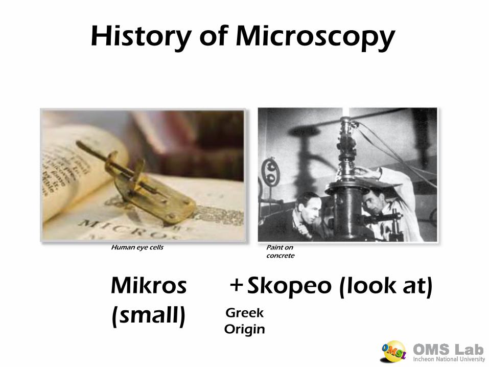
History of Microscopy
Paint on concrete
Human eye cells
Skopeo (look at) Greek
Origin
Mikros
(small)
+
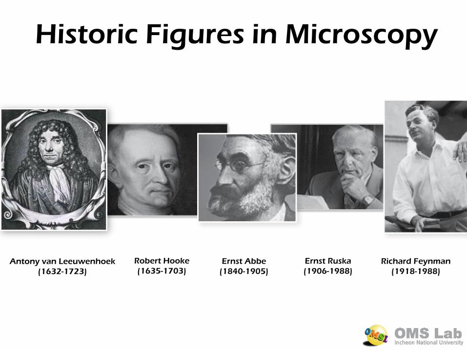
Historic Figures in Microscopy
Robert Hooke
(1635-1703)
Ernst Ruska
(1906-1988)
Ernst Abbe
(1840-1905)
Richard Feynman
(1918-1988)
Antony van Leeuwenhoek
(1632-1723)
Scanning probe
microscope
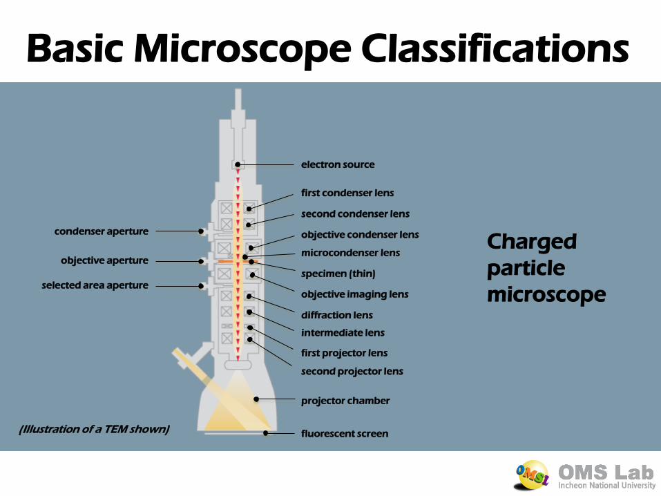
Basic Microscope Classifications
Charged particle microscope Optical (light) microscope
Optical (light)
microscope objective lens
light beam
specimen
light source
Scanning
probe
microscope
laser diode
X, Y piezoelectric
scanner
Z piezoelectric
scanner
cantilever
sample
(stationary)
mirror
multiple segmentphotodiode
(position sensitive detector)
Charged
particle
microscope
objective aperture
selected area aperture
condenser aperture
electron source
first condenser lens
second condenser lens
fluorescent screen
microcondenser lens
specimen (thin)
objective imaging lens
objective condenser lens
diffraction lens
intermediate lens
first projector lens
second projector lens
projector chamber
(Illustration of a TEM shown)
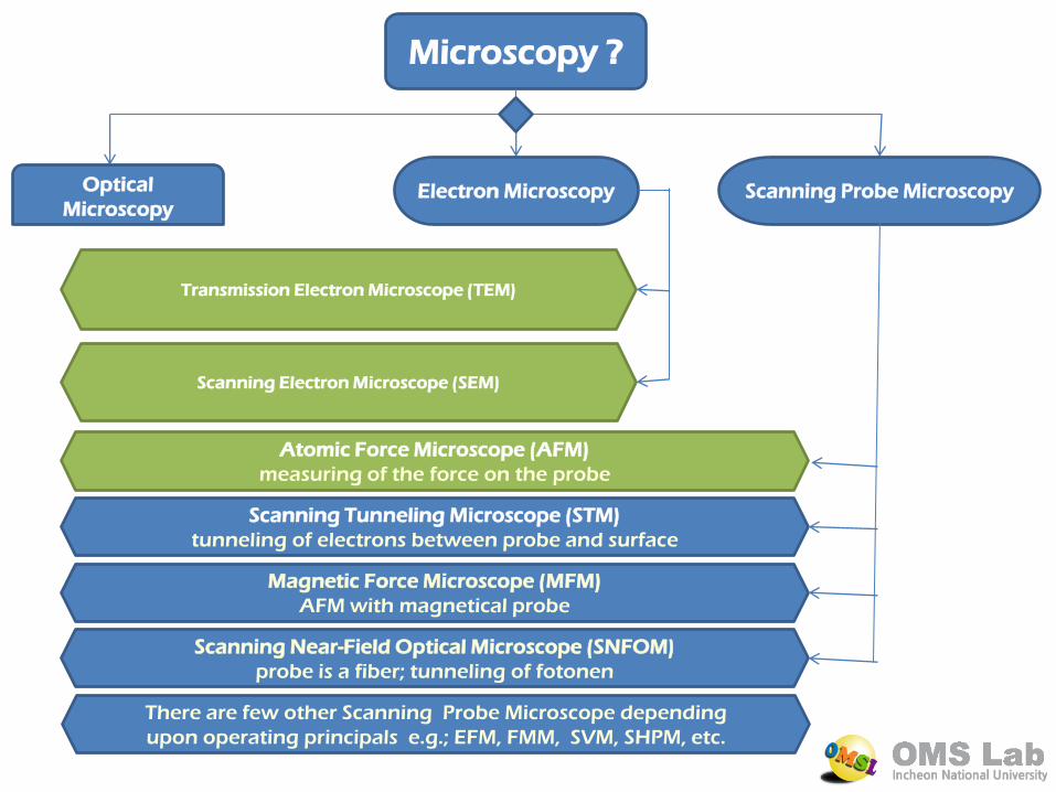
Microscopy ?
Optical
Microscopy Electron Microscopy Scanning Probe Microscopy
Scanning Electron Microscope (SEM)
Transmission Electron Microscope (TEM)
Atomic Force Microscope (AFM)
measuring of the force on the probe
Scanning Tunneling Microscope (STM)
tunneling of electrons between probe and surface
Magnetic Force Microscope (MFM)
AFM with magnetical probe
Scanning Near-Field Optical Microscope (SNFOM)
probe is a fiber; tunneling of fotonen
There are few other Scanning Probe Microscope depending
upon operating principals e.g.; EFM, FMM, SVM, SHPM, etc.
KEY CONCEPTS IN MICROSCOPY
• What is resolution and resolving power?
• What is an electron? – The electron gun
• Electromagnetic lenses
• The importance of vacuum technology
KEY CONCEPT: Resolution
Resolution is defined as the act, process, or capability of distinguis
hing between two separate, but adjacent objects or sou
rces of light, or between two nearly
equal wavelengths.
Resolving Power is the ability to make points or lines which are
closely adjacent in an object distinguishable in
an image.
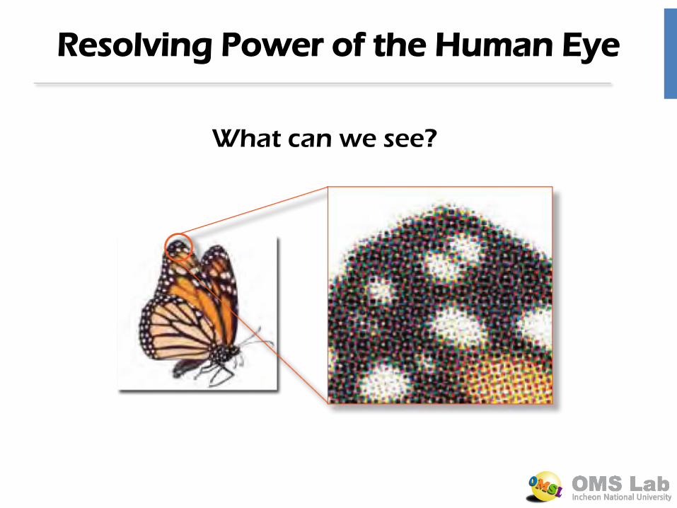
Resolving Power of the Human Eye
What can we see?
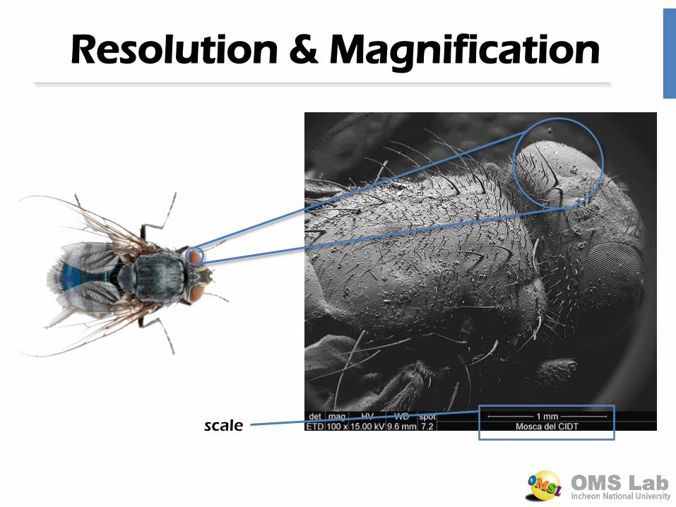
Resolution & Magnification
scale
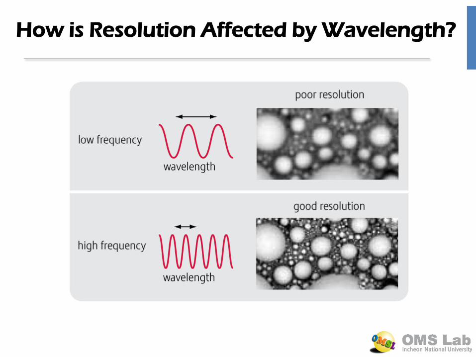
How is Resolution Affected by Wavelength?
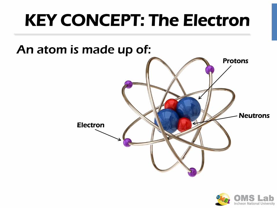
KEY CONCEPT: The Electron
An atom is made up of: Protons
Neutrons
Electron
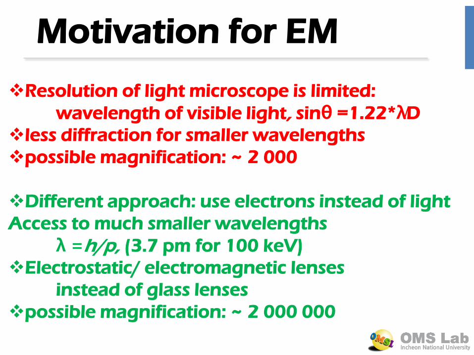
Motivation for EM
Resolution of light microscope is limited:
wavelength of visible light, sinθ =1.22*λ ̸D
less diffraction for smaller wavelengths
possible magnification: ~ 2 000
Different approach: use electrons instead of light
Access to much smaller wavelengths λ =h/p, (3.7 pm for 100 keV)
Electrostatic/ electromagnetic lenses
instead of glass lenses
possible magnification: ~ 2 000 000
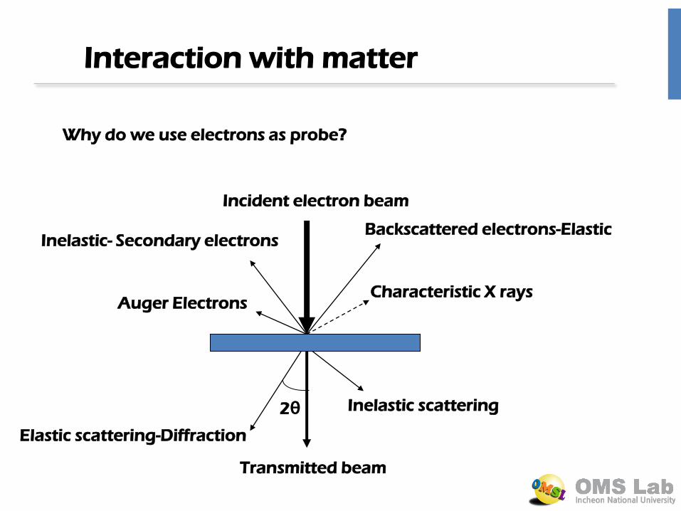
Interaction with matter
Why do we use electrons as probe?
Incident electron beam
Transmitted beam
Elastic scattering-Diffraction
Inelastic scattering
Auger Electrons
Backscattered electrons-Elastic
Characteristic X rays
Inelastic- Secondary electrons
2θ
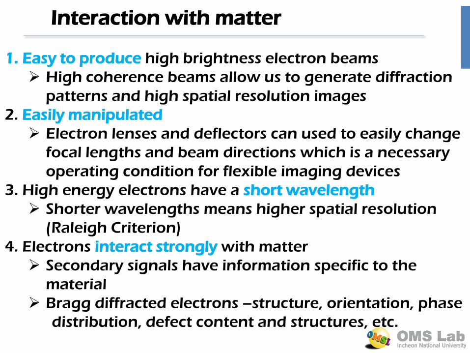
1. Easy to produce high brightness electron beams
High coherence beams allow us to generate diffraction
patterns and high spatial resolution images
2. Easily manipulated
Electron lenses and deflectors can used to easily change
focal lengths and beam directions which is a necessary
operating condition for flexible imaging devices
3. High energy electrons have a short wavelength
Shorter wavelengths means higher spatial resolution
(Raleigh Criterion)
4. Electrons interact strongly with matter
Secondary signals have information specific to the
material
Bragg diffracted electrons –structure, orientation, phase
distribution, defect content and structures, etc.
Interaction with matter
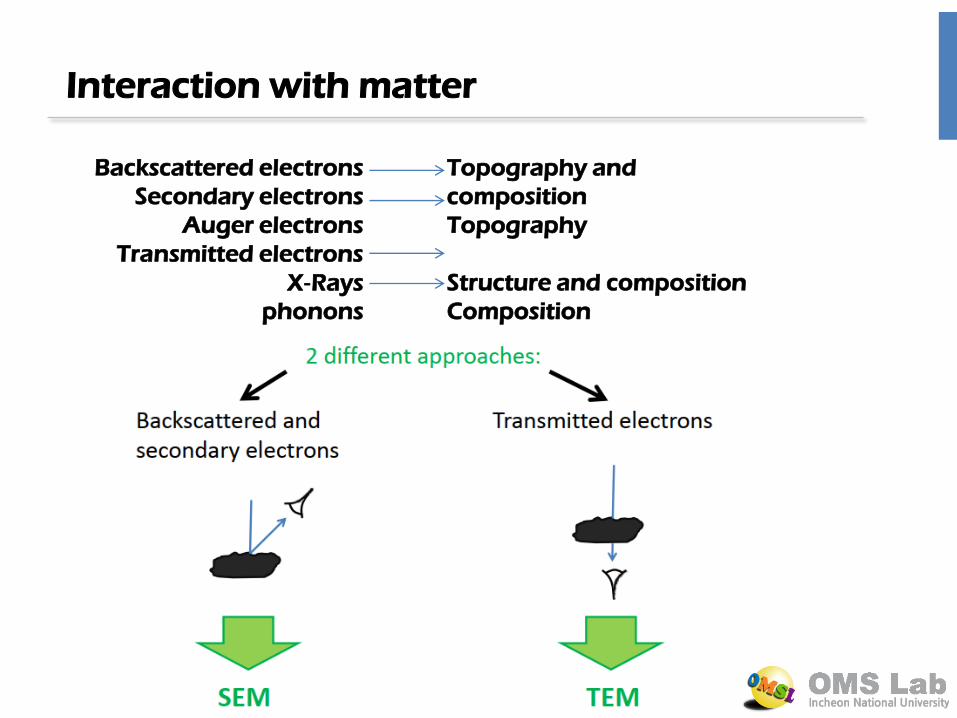
Interaction with matter
Backscattered electrons
Secondary electrons
Auger electrons
Transmitted electrons
X‐Rays
phonons
Topography and
composition
Topography
Structure and composition
Composition
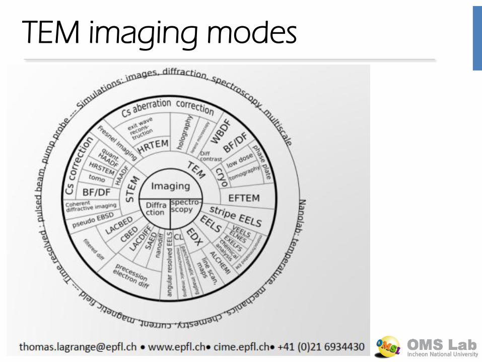
TEM imaging modes
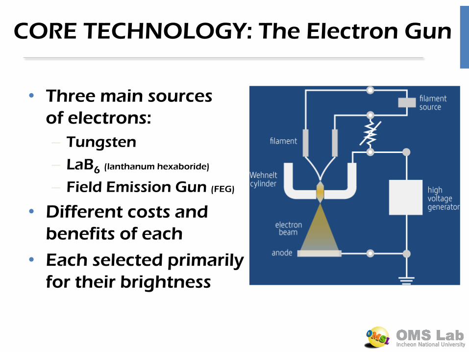
CORE TECHNOLOGY: The Electron Gun
• Three main sources
of electrons:
– Tungsten
– LaB6 (lanthanum hexaboride)
– Field Emission Gun (FEG)
• Different costs and
benefits of each
• Each selected primarily
for their brightness
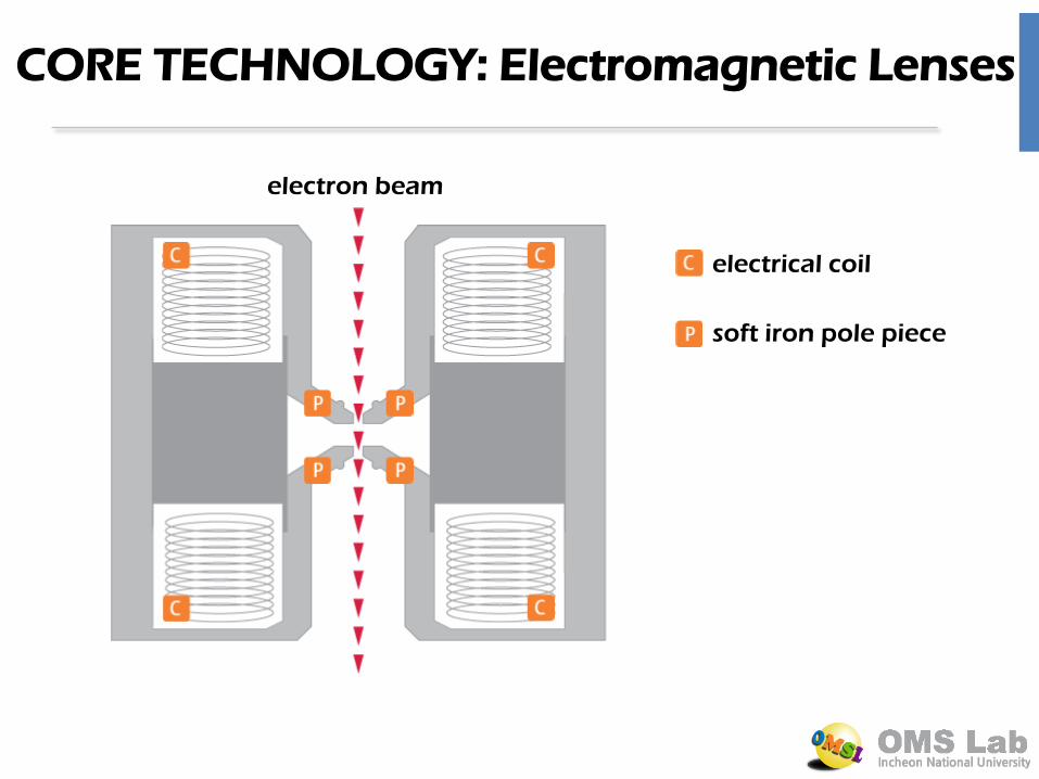
CORE TECHNOLOGY: Electromagnetic Lenses
electron beam
soft iron pole piece
electrical coil
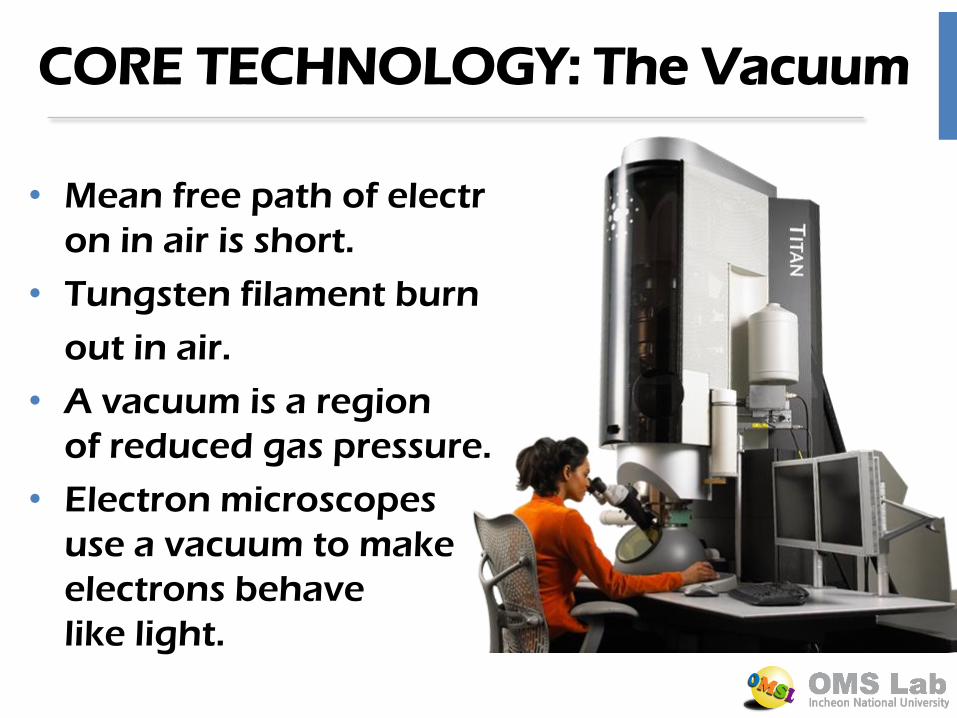
CORE TECHNOLOGY: The Vacuum
• Mean free path of electr
on in air is short.
• Tungsten filament burn
out in air.
• A vacuum is a region
of reduced gas pressure.
• Electron microscopes
use a vacuum to make
electrons behave
like light.
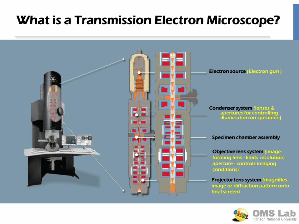
What is a Transmission Electron Microscope?
Projector lens system (magnifies
image or diffraction pattern onto
final screen)
Electron source (Electron gun )
Condenser system (lenses & apertures for controlling illumination on specimen)
Objective lens system (image-
forming lens - limits resolution;
aperture - controls imaging
conditions)
Specimen chamber assembly
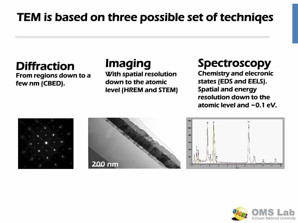
Imaging Diffraction Spectroscopy With spatial resolution
down to the atomic
level (HREM and STEM)
Chemistry and elecronic
states (EDS and EELS).
Spatial and energy
resolution down to the
atomic level and ~0.1 eV.
From regions down to a
few nm (CBED).
TEM is based on three possible set of techniqes
200 nm
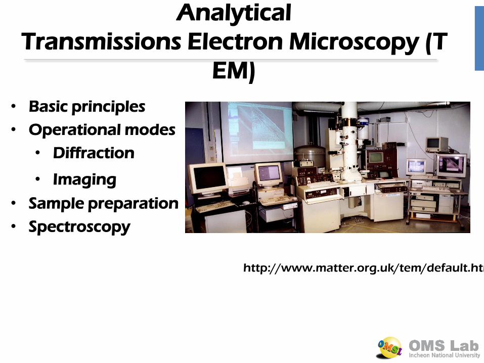
Analytical
Transmissions Electron Microscopy (T
EM)
• Basic principles
• Operational modes
• Diffraction
• Imaging
• Sample preparation
• Spectroscopy
http://www.matter.org.uk/tem/default.htm
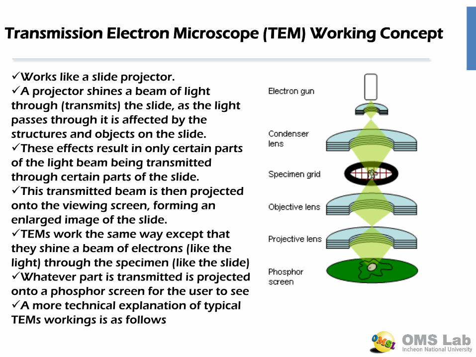
Works like a slide projector.
A projector shines a beam of light
through (transmits) the slide, as the light
passes through it is affected by the
structures and objects on the slide.
These effects result in only certain parts
of the light beam being transmitted
through certain parts of the slide.
This transmitted beam is then projected
onto the viewing screen, forming an
enlarged image of the slide.
TEMs work the same way except that
they shine a beam of electrons (like the
light) through the specimen (like the slide).
Whatever part is transmitted is projected
onto a phosphor screen for the user to see.
A more technical explanation of typical
TEMs workings is as follows
Transmission Electron Microscope (TEM) Working Concept
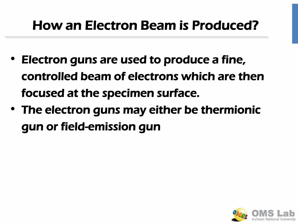
How an Electron Beam is Produced?
• Electron guns are used to produce a fine,
controlled beam of electrons which are then
focused at the specimen surface.
• The electron guns may either be thermionic
gun or field-emission gun
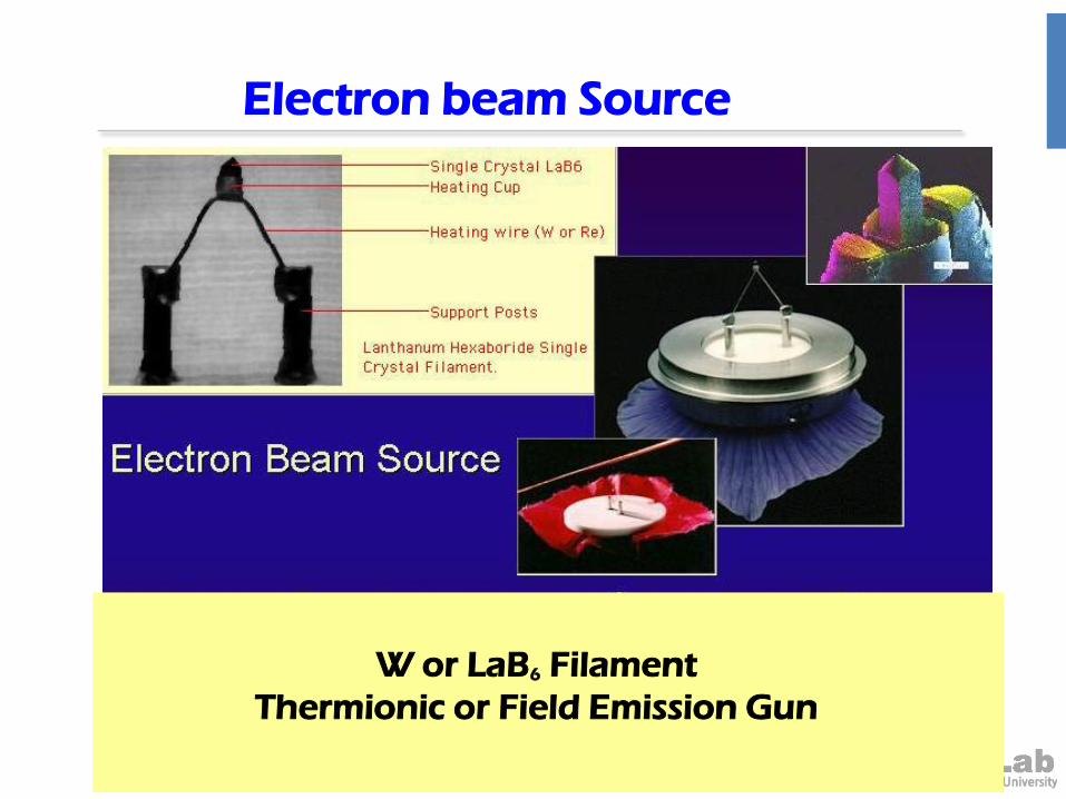
Electron beam Source
W or LaB6 Filament
Thermionic or Field Emission Gun
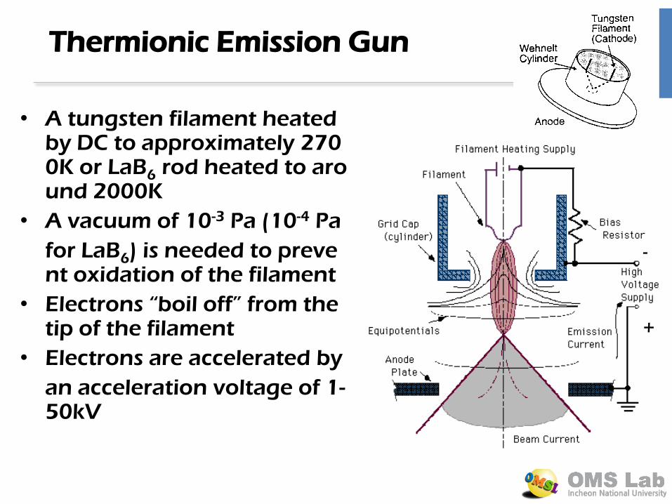
Thermionic Emission Gun
• A tungsten filament heated by DC to approximately 2700K or LaB6 rod heated to around 2000K
• A vacuum of 10-3 Pa (10-4 Pa
for LaB6) is needed to prevent oxidation of the filament
• Electrons “boil off” from the tip of the filament
• Electrons are accelerated by
an acceleration voltage of 1-50kV
-
+
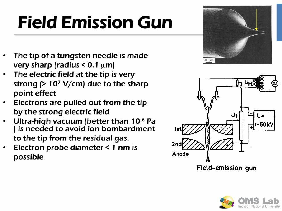
Field Emission Gun
• The tip of a tungsten needle is made
very sharp (radius < 0.1 m)
• The electric field at the tip is very
strong (> 107 V/cm) due to the sharp
point effect
• Electrons are pulled out from the tip
by the strong electric field
• Ultra-high vacuum (better than 10-6 Pa) is needed to avoid ion bombardment
to the tip from the residual gas.
• Electron probe diameter < 1 nm is
possible
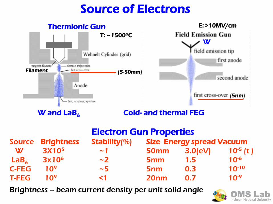
Source of Electrons
T: ~1500oC
Thermionic Gun
W and LaB6 Cold- and thermal FEG
Electron Gun Properties Source Brightness Stability(%) Size Energy spread Vacuum
W 3X10⁵ ~1 50mm 3.0(eV) 10-5 (t )
LaB6 3x10⁶ ~2 5mm 1.5 10-6
C-FEG 109 ~5 5nm 0.3 10-10
T-FEG 109 <1 20nm 0.7 10-9
(5-50mm)
E: >10MV/cm
(5nm)
Filament
W
Brightness – beam current density per unit solid angle
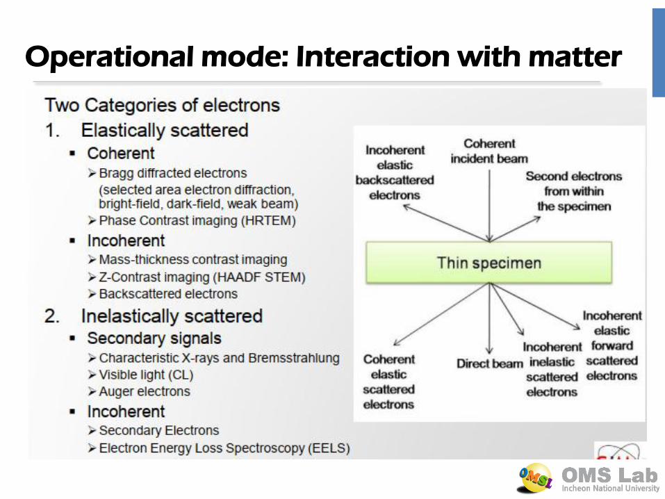
Operational mode: Interaction with matter
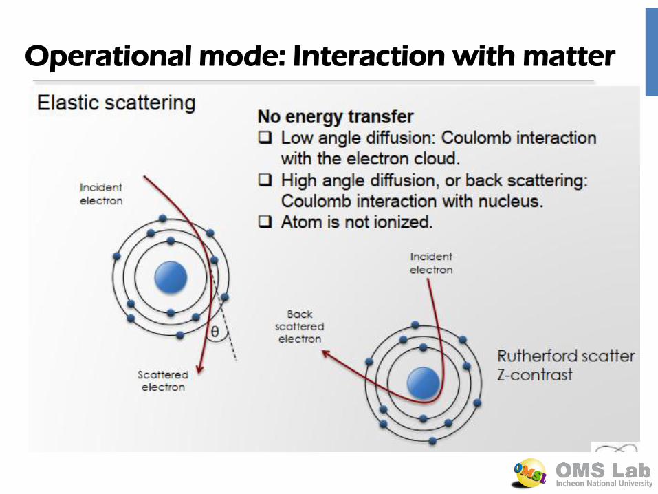
Operational mode: Interaction with matter
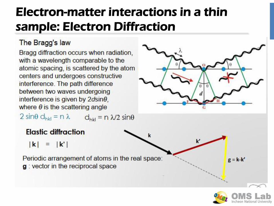
Electron-matter interactions in a thin
sample: Electron Diffraction
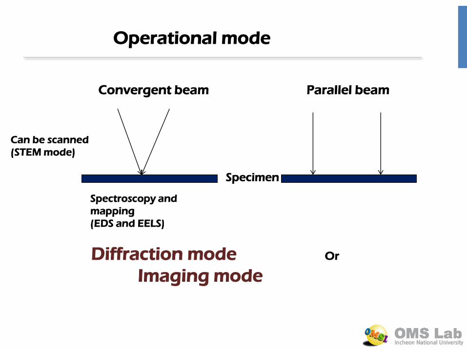
Convergent beam Parallel beam
Can be scanned
(STEM mode)
Specimen
Diffraction mode Or
Imaging mode
Spectroscopy and
mapping
(EDS and EELS)
Operational mode
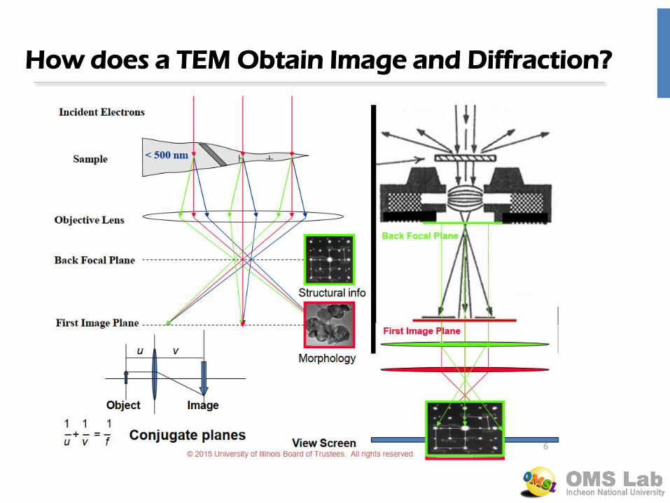
How does a TEM Obtain Image and Diffraction?
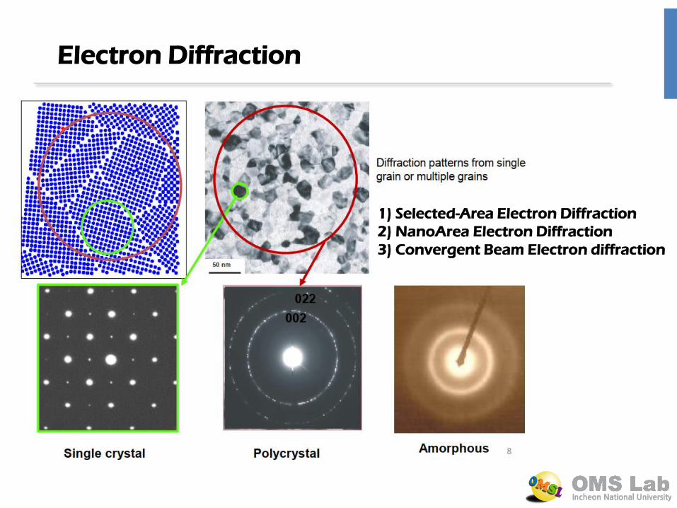
Electron Diffraction
1) Selected-Area Electron Diffraction
2) NanoArea Electron Diffraction
3) Convergent Beam Electron diffraction
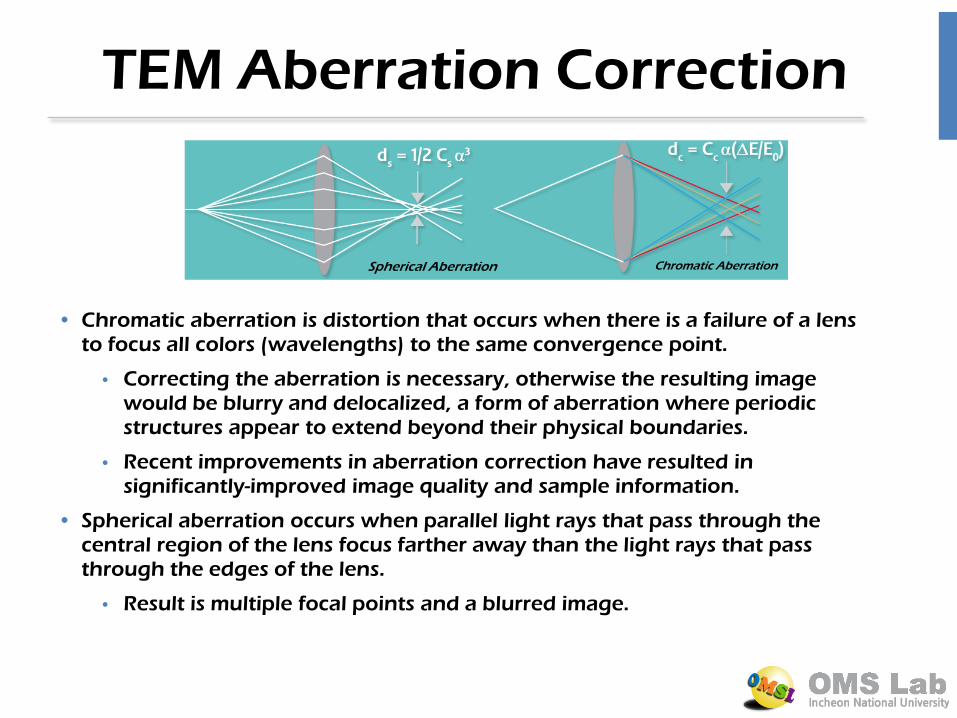
TEM Aberration Correction
• Chromatic aberration is distortion that occurs when there is a failure of a lens to focus all colors (wavelengths) to the same convergence point.
• Correcting the aberration is necessary, otherwise the resulting image would be blurry and delocalized, a form of aberration where periodic structures appear to extend beyond their physical boundaries.
• Recent improvements in aberration correction have resulted in significantly-improved image quality and sample information.
• Spherical aberration occurs when parallel light rays that pass through the central region of the lens focus farther away than the light rays that pass through the edges of the lens.
• Result is multiple focal points and a blurred image.
Chromatic Aberration Spherical Aberration
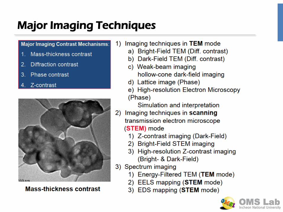
Major Imaging Techniques
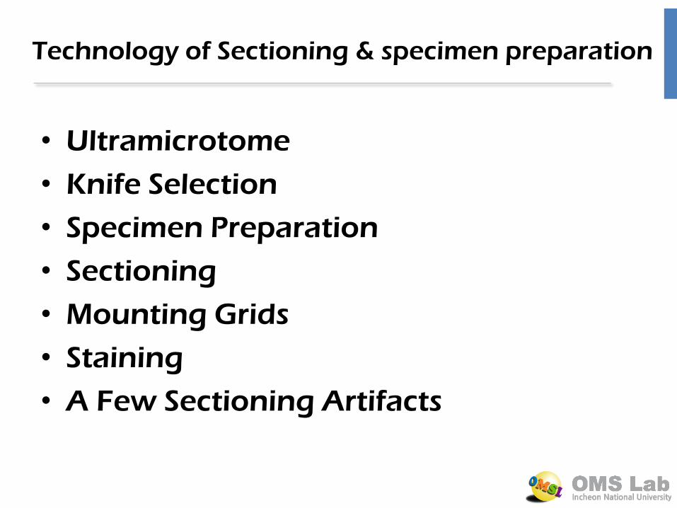
Technology of Sectioning & specimen preparation
• Ultramicrotome
• Knife Selection
• Specimen Preparation
• Sectioning
• Mounting Grids
• Staining
• A Few Sectioning Artifacts
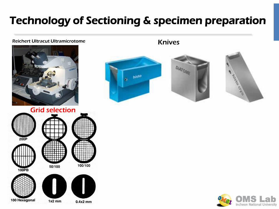
Grid selection
Knives Reichert Ultracut Ultramicrotome
Technology of Sectioning & specimen preparation
Technology of specimen preparation • Coarse preparation of samples:
– Small objects (mounted on grids): • Strew
• Spray
• Cleave
• Crush
– Disc cutter (optionally mounted on grids)
– Grinding device
• Intermediate preparation: – Dimple grinder
• Fine preparation: – Chemical polisher
– Electropolisher
– Ion thinning mill • PIMS: precision milling (using SEM on very small areas (1 X 1 μm2)
• PIPS: precision ion polishing (at 4° angle) removes surface roughness with minimum surface damage
• Beam blockers may be needed to mask epoxy or easily etched areas
• Each technique has its own disadvantages and potential artifact
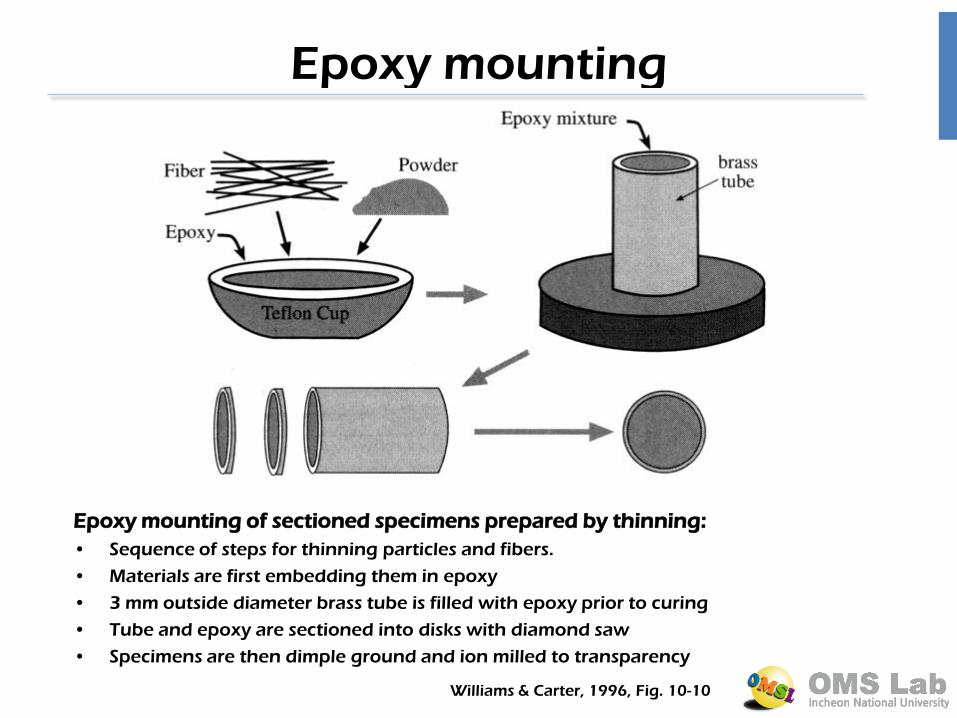
Epoxy mounting
Williams & Carter, 1996, Fig. 10-10
Epoxy mounting of sectioned specimens prepared by thinning:
• Sequence of steps for thinning particles and fibers.
• Materials are first embedding them in epoxy
• 3 mm outside diameter brass tube is filled with epoxy prior to curing
• Tube and epoxy are sectioned into disks with diamond saw
• Specimens are then dimple ground and ion milled to transparency
Scientific Reports volume4, Article number: 6486 (2014)
Scientific Reports volume5,
Article number: 16219 (2015)
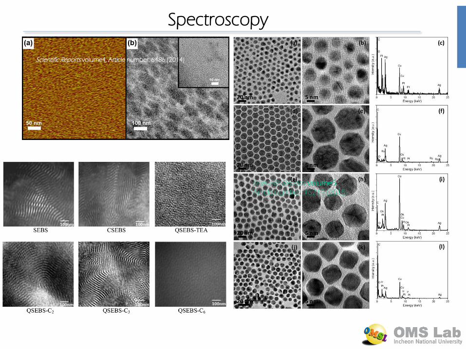
Spectroscopy
Scanning Electron Microscope (SEM)
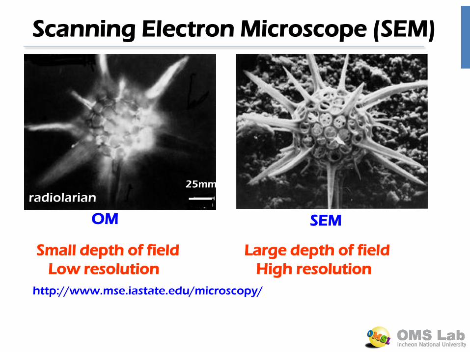
25mm
OM SEM
Small depth of field
Low resolution
Large depth of field
High resolution
radiolarian
http://www.mse.iastate.edu/microscopy/
Scanning Electron Microscope (SEM)
What is SEM?
Working principles of SEM
Major components and their functions
Electron beam - specimen interactions
Interaction volume and escape volume
Magnification, resolution, depth of field and image contrast
Energy Dispersive X-ray Spectroscopy (EDS)
Wavelength Dispersive X-ray Spectroscopy (WDS)
Orientation Imaging Microscopy (OIM)
X-ray Fluorescence (XRF)
Scanning Electron Microscope
Instead of using the full-field image, a point-to-point
measurement strategy is used.
High energy electron beam is used to excite the
specimen and the signals are collected and analyzed
so that an image can be constructed.
The signals carry topological, chemical and
crystallographic information, respectively, of the
samples surface.
http://www.youtube.com/watch?v=lrXMIghANbg at~4:16-4:42
https://www.youtube.com/watch?v=VWxYsZPtTsI at~4:18-4:38
https://www.youtube.com/watch?v=nPskvGJKtDI
– a Totally Different Imaging Concept
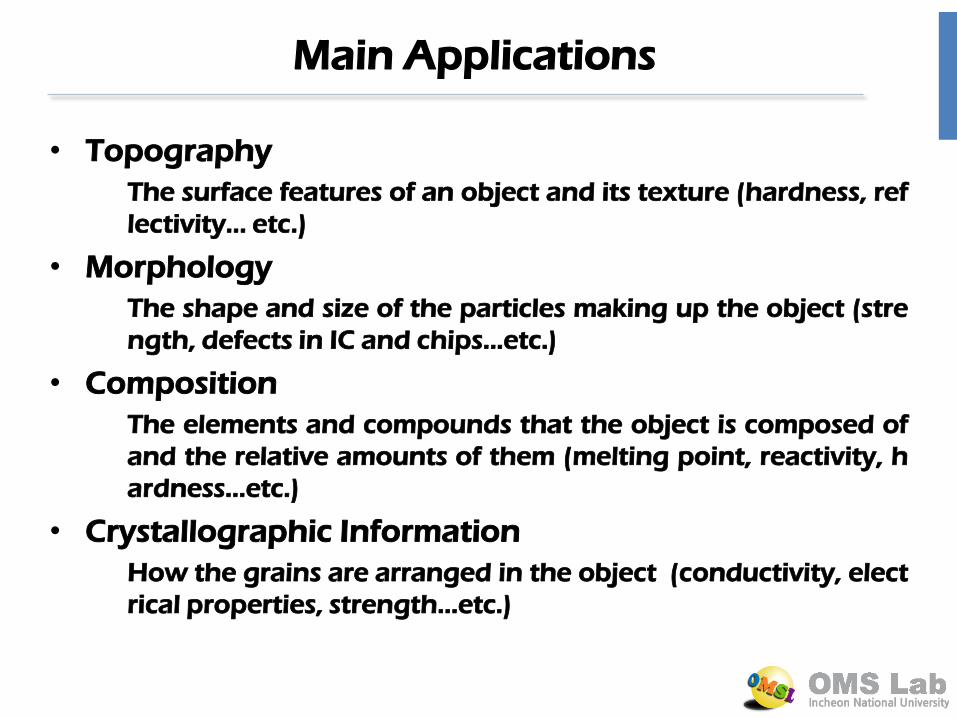
Main Applications
• Topography
The surface features of an object and its texture (hardness, ref
lectivity… etc.)
• Morphology
The shape and size of the particles making up the object (stre
ngth, defects in IC and chips...etc.)
• Composition
The elements and compounds that the object is composed of
and the relative amounts of them (melting point, reactivity, h
ardness...etc.)
• Crystallographic Information
How the grains are arranged in the object (conductivity, elect
rical properties, strength...etc.)
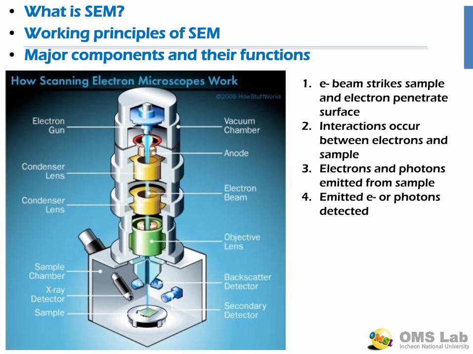
• What is SEM?
• Working principles of SEM
• Major components and their functions
1. e- beam strikes sample
and electron penetrate
surface
2. Interactions occur
between electrons and
sample
3. Electrons and photons
emitted from sample
4. Emitted e- or photons
detected
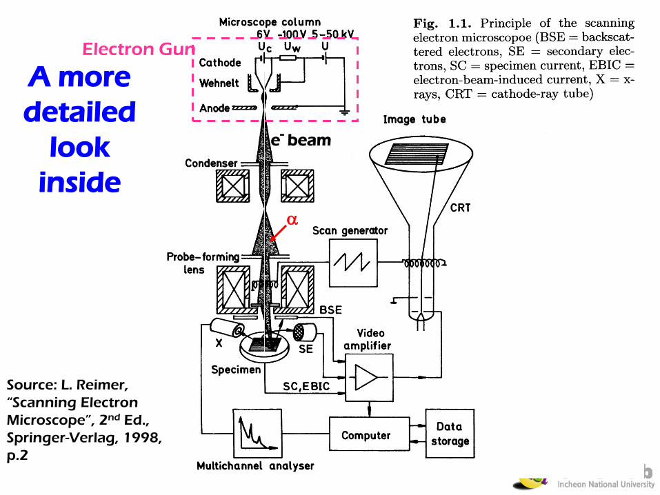
A more
detailed
look
inside
Source: L. Reimer,
“Scanning Electron
Microscope”, 2nd Ed.,
Springer-Verlag, 1998,
p.2
Electron Gun
e- beam
beam e-
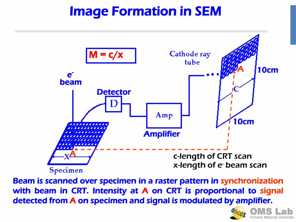
Beam is scanned over specimen in a raster pattern in synchronization
with beam in CRT. Intensity at A on CRT is proportional to signal
detected from A on specimen and signal is modulated by amplifier.
A
A
Detector
Amplifier
10cm
10cm
Image Formation in SEM
M = c/x
c-length of CRT scan x-length of e- beam scan
How Is Electron Beam Focused?
A magnetic lens is a solenoid designed to produce a specific
magnetic flux distribution.
p
q
Magnetic lens (solenoid)
Lens formula: 1/f = 1/p + 1/q
M = q/p Demagnification:
(Beam diameter)
F = -e(v x B)
f Bo2
f can be adjusted by changing Bo, i.e., changing the current through coil.
1 1 1
_ = _ + _
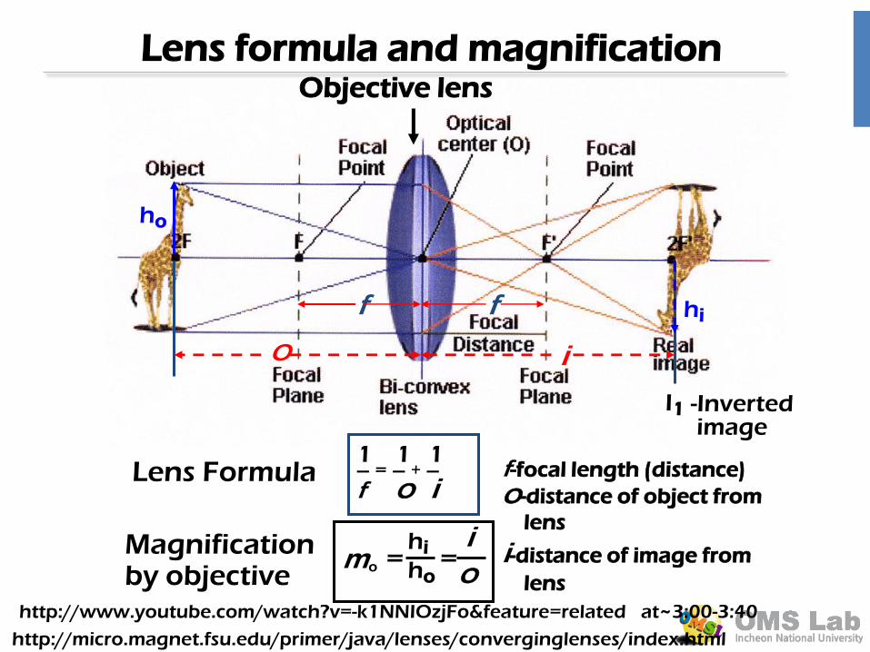
f O i Lens Formula f-focal length (distance)
O-distance of object from
lens
i-distance of image from
lens
I1
O i
i
O = = mo
Magnification by objective
Lens formula and magnification Objective lens
-Inverted image
f f
ho
hi
hi
ho
http://micro.magnet.fsu.edu/primer/java/lenses/converginglenses/index.html
http://www.youtube.com/watch?v=-k1NNIOzjFo&feature=related at~3:00-3:40
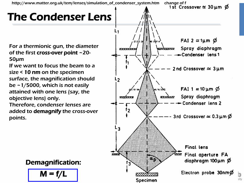
The Condenser Lens
Demagnification:
M = f/L
http://www.matter.org.uk/tem/lenses/simulation_of_condenser_system.htm change of f
For a thermionic gun, the diameter
of the first cross-over point ~20-
50µm
If we want to focus the beam to a
size < 10 nm on the specimen
surface, the magnification should
be ~1/5000, which is not easily
attained with one lens (say, the
objective lens) only.
Therefore, condenser lenses are
added to demagnify the cross-over
points.
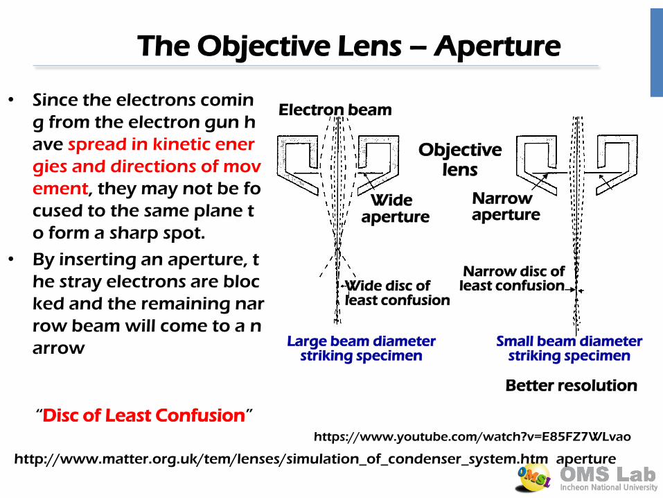
The Objective Lens – Aperture
• Since the electrons comin
g from the electron gun h
ave spread in kinetic ener
gies and directions of mov
ement, they may not be fo
cused to the same plane t
o form a sharp spot.
• By inserting an aperture, t
he stray electrons are bloc
ked and the remaining nar
row beam will come to a n
arrow
“Disc of Least Confusion”
Electron beam
Objective lens
Wide aperture
Narrow aperture
Wide disc of least confusion
Narrow disc of least confusion
Large beam diameter striking specimen
Small beam diameter striking specimen
http://www.matter.org.uk/tem/lenses/simulation_of_condenser_system.htm aperture
Better resolution
https://www.youtube.com/watch?v=E85FZ7WLvao
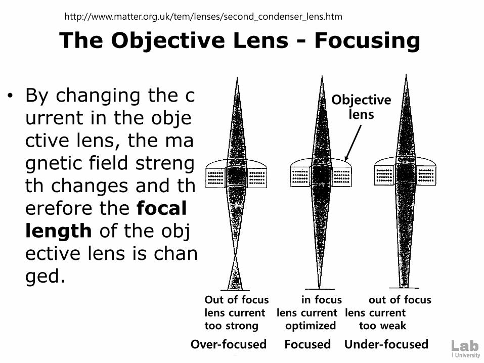
The Objective Lens - Focusing
• By changing the current in the objective lens, the magnetic field strength changes and therefore the focal length of the objective lens is changed.
Out of focus in focus out of focus lens current lens current lens current too strong optimized too weak
Objective lens
http://www.matter.org.uk/tem/lenses/second_condenser_lens.htm
Over-focused Focused Under-focused
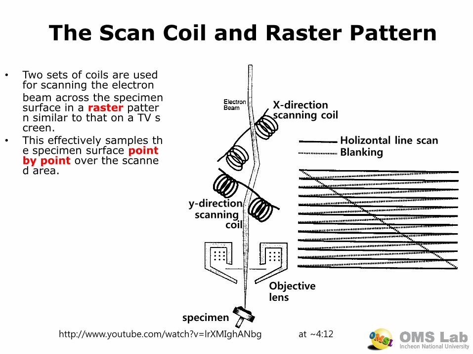
The Scan Coil and Raster Pattern
• Two sets of coils are used for scanning the electron
beam across the specimen surface in a raster pattern similar to that on a TV screen.
• This effectively samples the specimen surface point by point over the scanned area.
X-direction scanning coil
y-direction scanning
coil
specimen
Objective lens
Holizontal line scan Blanking
http://www.youtube.com/watch?v=lrXMIghANbg at ~4:12
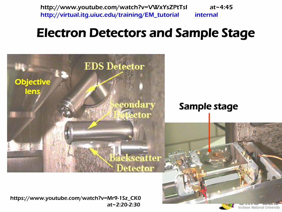
Electron Detectors and Sample Stage
Objective
lens
Sample stage
http://www.youtube.com/watch?v=VWxYsZPtTsI at~4:45
http://virtual.itg.uiuc.edu/training/EM_tutorial internal
https://www.youtube.com/watch?v=Mr9-1Sz_CK0
at~2:20-2:30
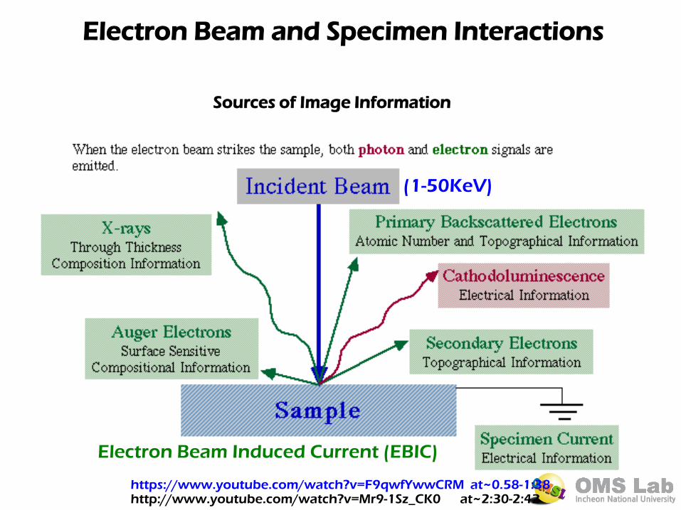
Electron Beam and Specimen Interactions
Electron/Specimen Interactions Sources of Image Information
(1-50KeV)
Electron Beam Induced Current (EBIC)
http://www.youtube.com/watch?v=Mr9-1Sz_CK0 at~2:30-2:42 https://www.youtube.com/watch?v=F9qwfYwwCRM at~0.58-1:38
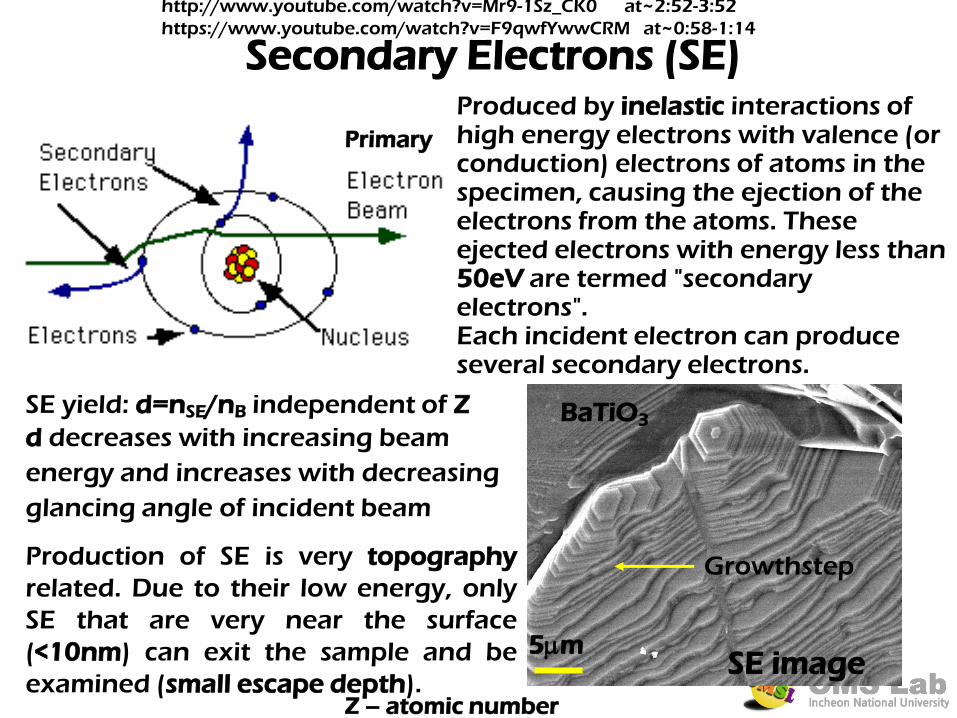
Secondary Electrons (SE) Produced by inelastic interactions of high energy electrons with valence (or conduction) electrons of atoms in the specimen, causing the ejection of the electrons from the atoms. These ejected electrons with energy less than 50eV are termed "secondary electrons". Each incident electron can produce several secondary electrons.
Production of SE is very topography
related. Due to their low energy, only
SE that are very near the surface
(<10nm) can exit the sample and be
examined (small escape depth).
Growthstep
BaTiO3
5m SE image
Primary
SE yield: d=nSE/nB independent of Z
d decreases with increasing beam
energy and increases with decreasing
glancing angle of incident beam
Z – atomic number
http://www.youtube.com/watch?v=Mr9-1Sz_CK0 at~2:52-3:52
https://www.youtube.com/watch?v=F9qwfYwwCRM at~0:58-1:14
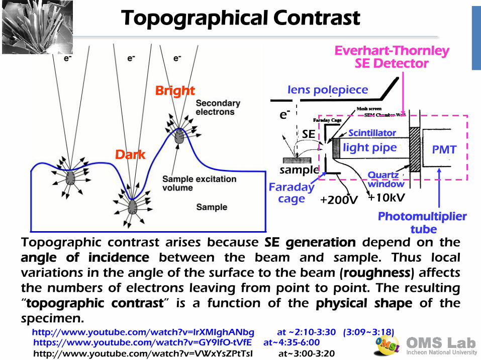
Topographical Contrast
Bright
Dark
+200V
e-
lens polepiece
SE
sample
Everhart-Thornley SE Detector
Scintillator
light pipe
Quartz window
+10kV Faraday
cage
Photomultiplier tube
PMT
http://www.youtube.com/watch?v=lrXMIghANbg at ~2:10-3:30 (3:09~3:18)
Topographic contrast arises because SE generation depend on the angle of incidence between the beam and sample. Thus local variations in the angle of the surface to the beam (roughness) affects the numbers of electrons leaving from point to point. The resulting “topographic contrast” is a function of the physical shape of the specimen.
https://www.youtube.com/watch?v=GY9lfO-tVfE at~4:35-6:00
http://www.youtube.com/watch?v=VWxYsZPtTsI at~3:00-3:20
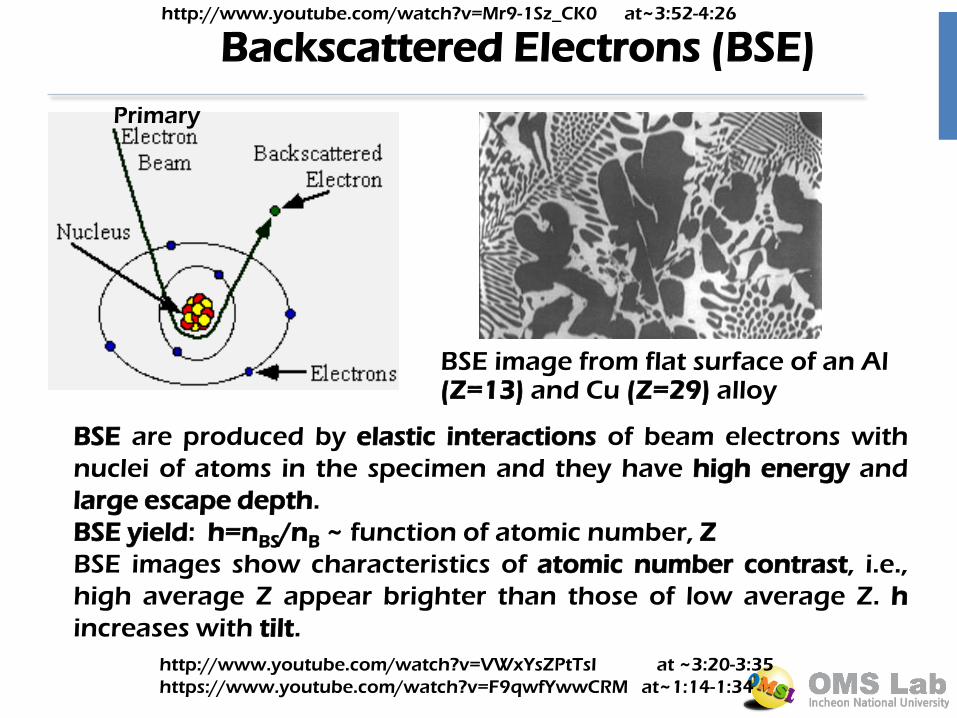
Backscattered Electrons (BSE)
BSE are produced by elastic interactions of beam electrons with
nuclei of atoms in the specimen and they have high energy and
large escape depth.
BSE yield: h=nBS/nB ~ function of atomic number, Z
BSE images show characteristics of atomic number contrast, i.e.,
high average Z appear brighter than those of low average Z. h
increases with tilt.
Primary
BSE image from flat surface of an Al (Z=13) and Cu (Z=29) alloy
http://www.youtube.com/watch?v=VWxYsZPtTsI at ~3:20-3:35
https://www.youtube.com/watch?v=F9qwfYwwCRM at~1:14-1:34
http://www.youtube.com/watch?v=Mr9-1Sz_CK0 at~3:52-4:26
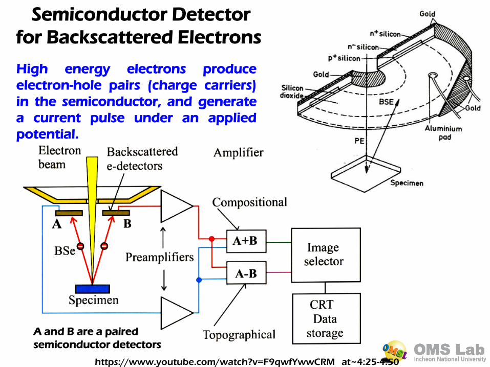
Semiconductor Detector
for Backscattered Electrons
High energy electrons produce
electron-hole pairs (charge carriers)
in the semiconductor, and generate
a current pulse under an applied
potential.
A and B are a paired
semiconductor detectors
https://www.youtube.com/watch?v=F9qwfYwwCRM at~4:25-4:50
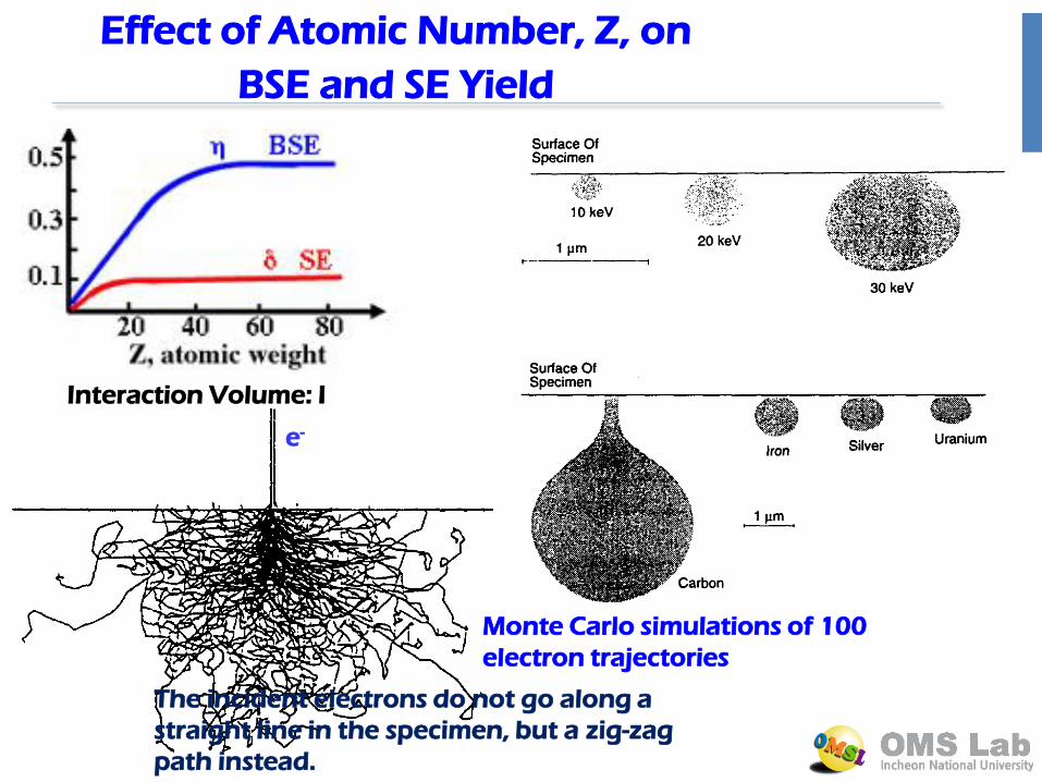
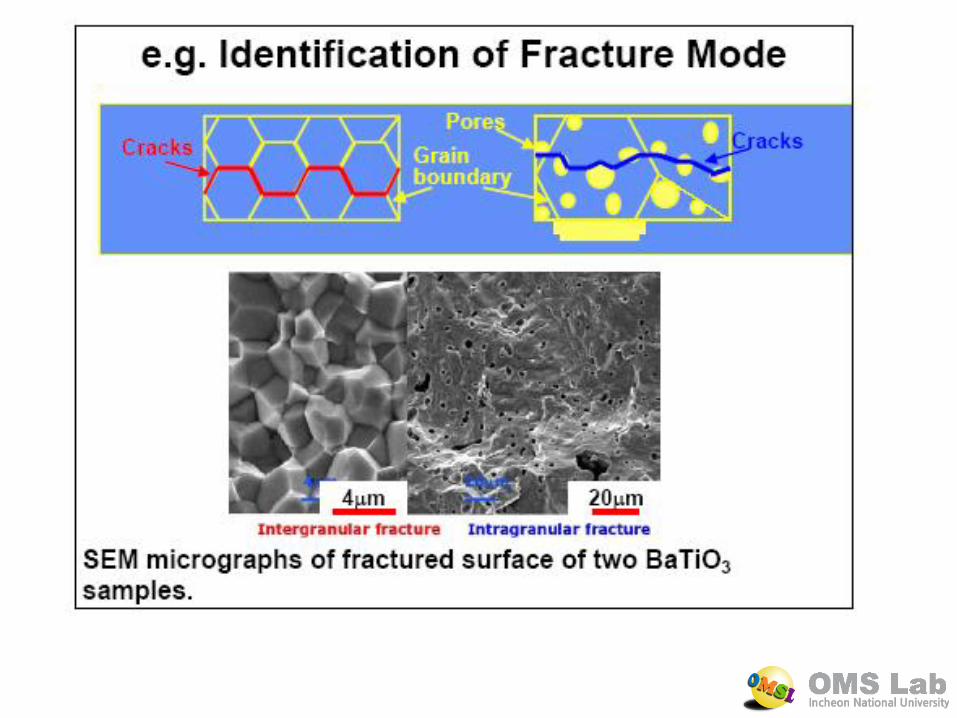
Effect of Atomic Number, Z, on
BSE and SE Yield
Monte Carlo simulations of 100
electron trajectories
e-
Interaction Volume: I
The incident electrons do not go along a
straight line in the specimen, but a zig-zag
path instead.
Escape Volume of Various Signals
• The incident electrons interact with specimen atoms along their path in the specimen and generate various signals.
• Owing to the difference in energy of these signals, their ‘penetration depths’ are different
• Therefore different signal observable on the specimen surface comes from different parts of the interaction volume
• The volume responsible for the respective signal is called the escape volume of that signal.
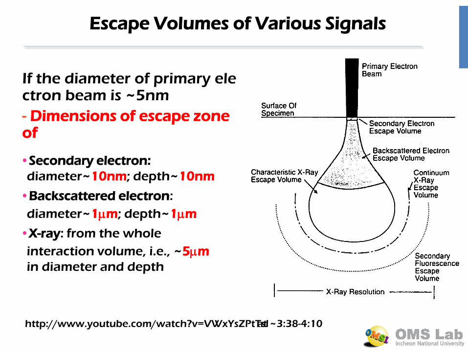
If the diameter of primary electron beam is ~5nm
- Dimensions of escape zone of
Escape Volumes of Various Signals
•Secondary electron:
diameter~10nm; depth~10nm
•Backscattered electron:
diameter~1m; depth~1m
•X-ray: from the whole
interaction volume, i.e., ~5m
in diameter and depth
http://www.youtube.com/watch?v=VWxYsZPtTsI at ~3:38-4:10
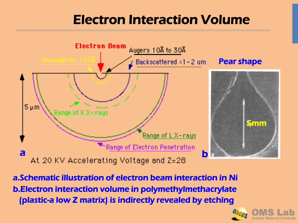
Electron Interaction Volume
5mm
a b
a.Schematic illustration of electron beam interaction in Ni
b.Electron interaction volume in polymethylmethacrylate
(plastic-a low Z matrix) is indirectly revealed by etching
Pear shape
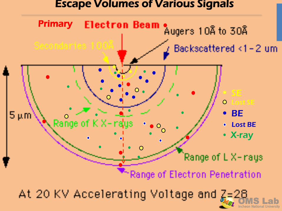
Escape Volumes of Various Signals
SE
BE
X-ray
Lost SE
Lost BE
Primary
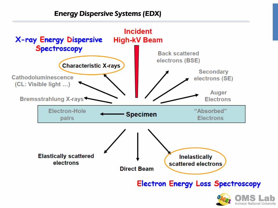
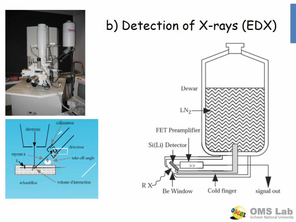
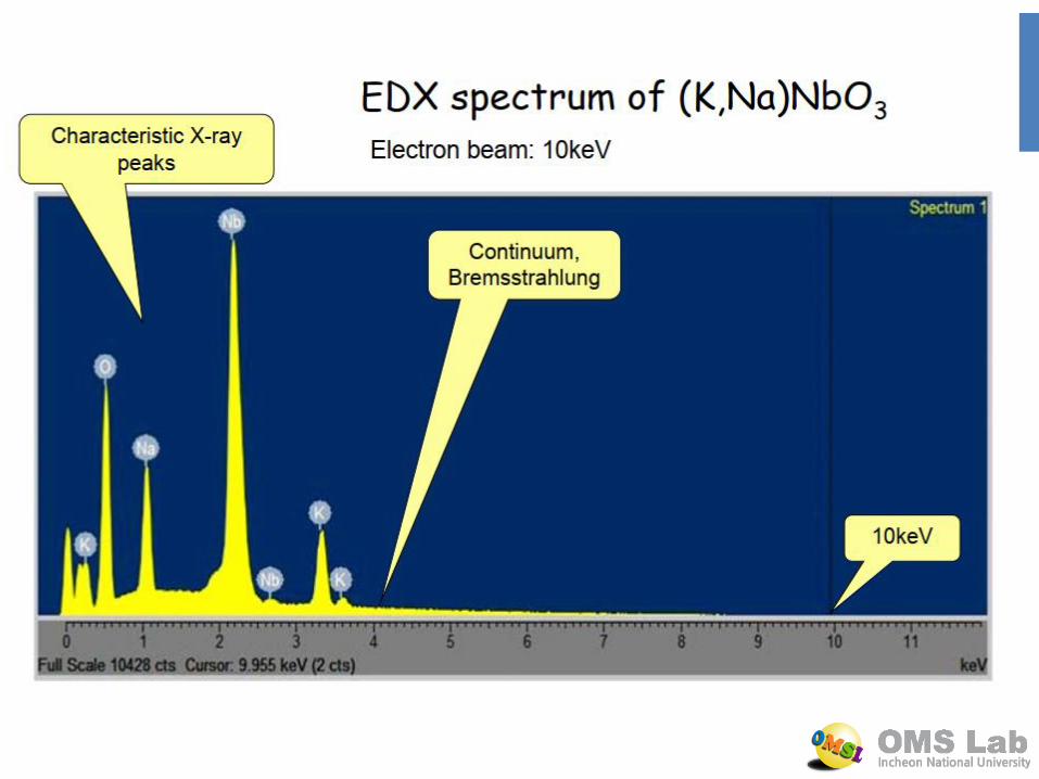
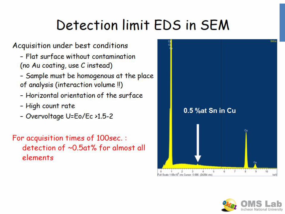
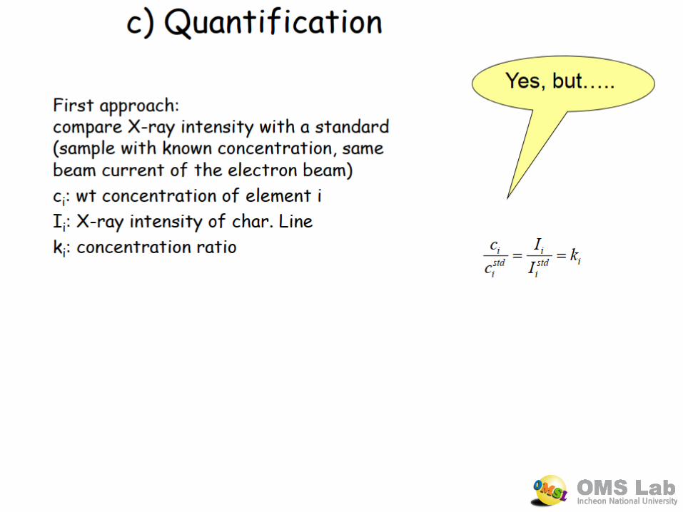
Energy Dispersive Systems (EDX)
a) Generation of X-ray
b) Mechanism of EDX
c) Detection
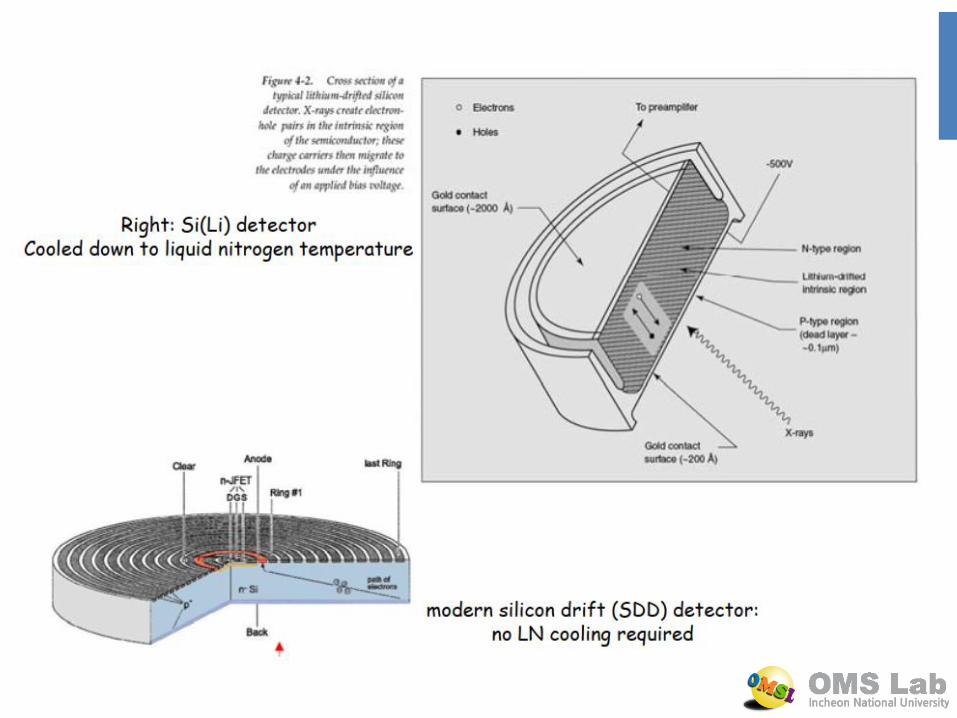
Si(Li) Detector, EDS (<-> WDS)
d) Quantification
EDX in SEM, Interaction volume
Monte-Carlo-Simulations
EDX in TEM
e) Examples
Basics of EDX
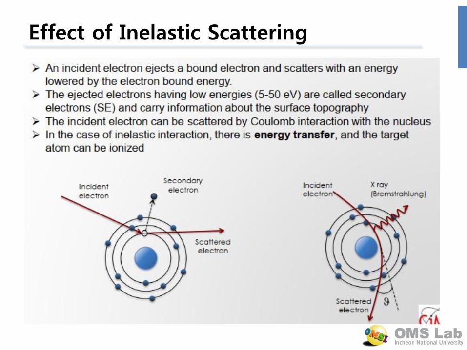
Effect of Inelastic Scattering
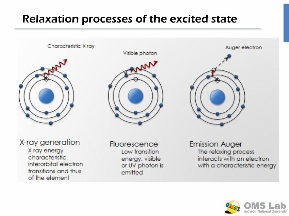
Relaxation processes of the excited state
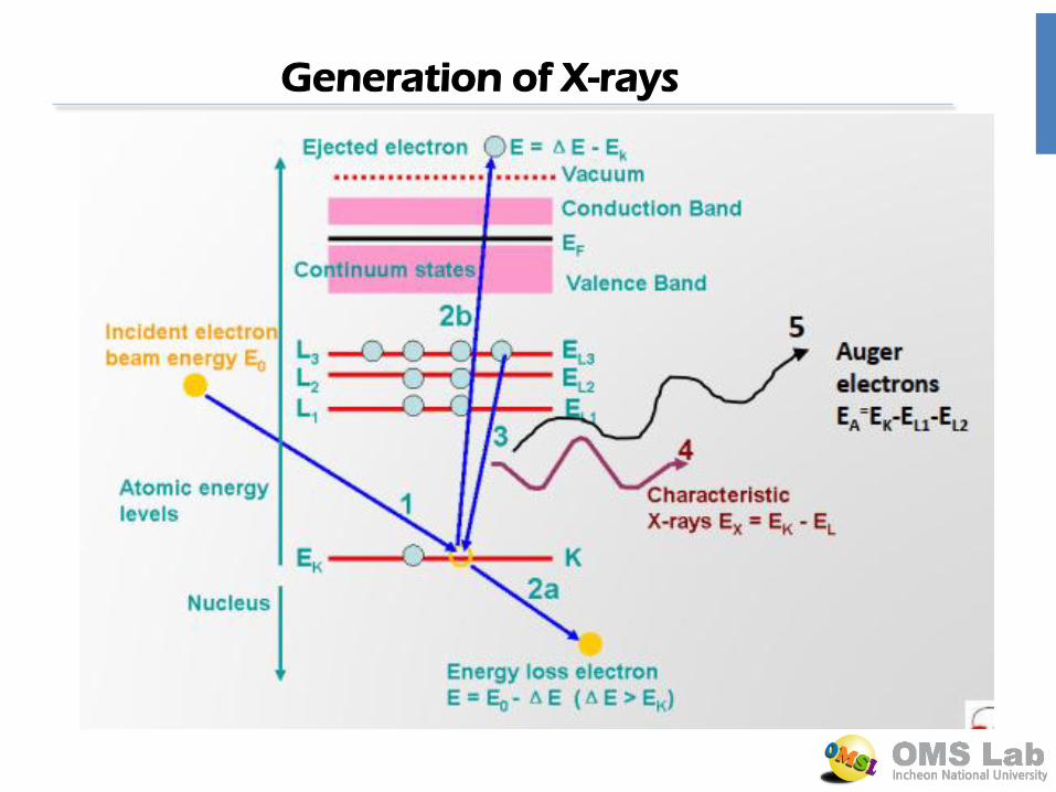
Generation of X-rays
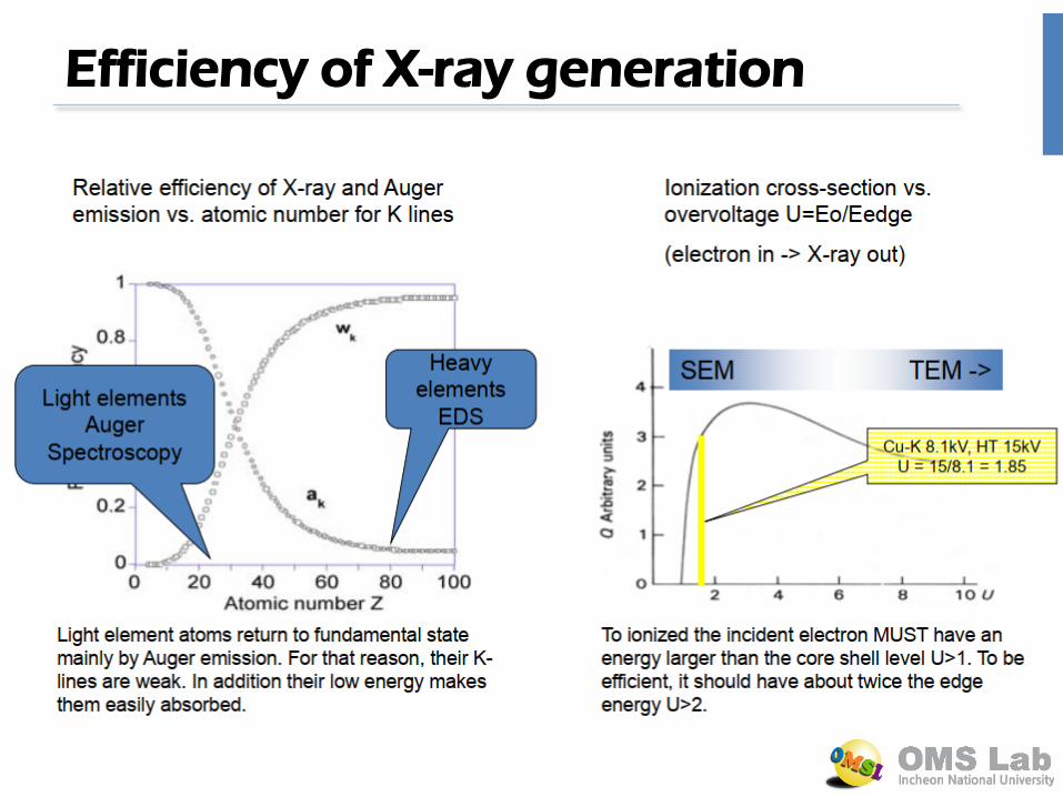
Efficiency of X-ray generation
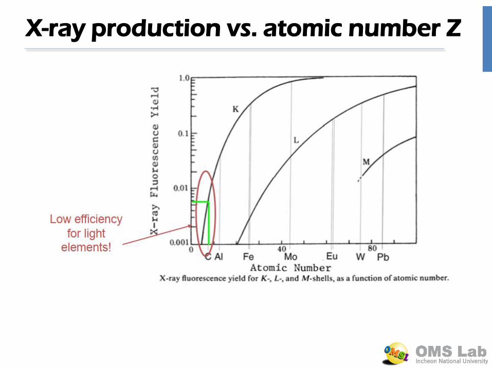
X-ray production vs. atomic number Z
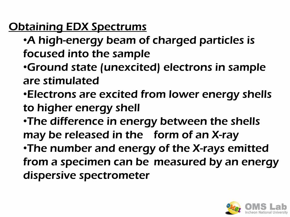
Obtaining EDX Spectrums
•A high-energy beam of charged particles is
focused into the sample
•Ground state (unexcited) electrons in sample
are stimulated
•Electrons are excited from lower energy shells
to higher energy shell
•The difference in energy between the shells
may be released in the form of an X-ray
•The number and energy of the X-rays emitted
from a specimen can be measured by an energy
dispersive spectrometer
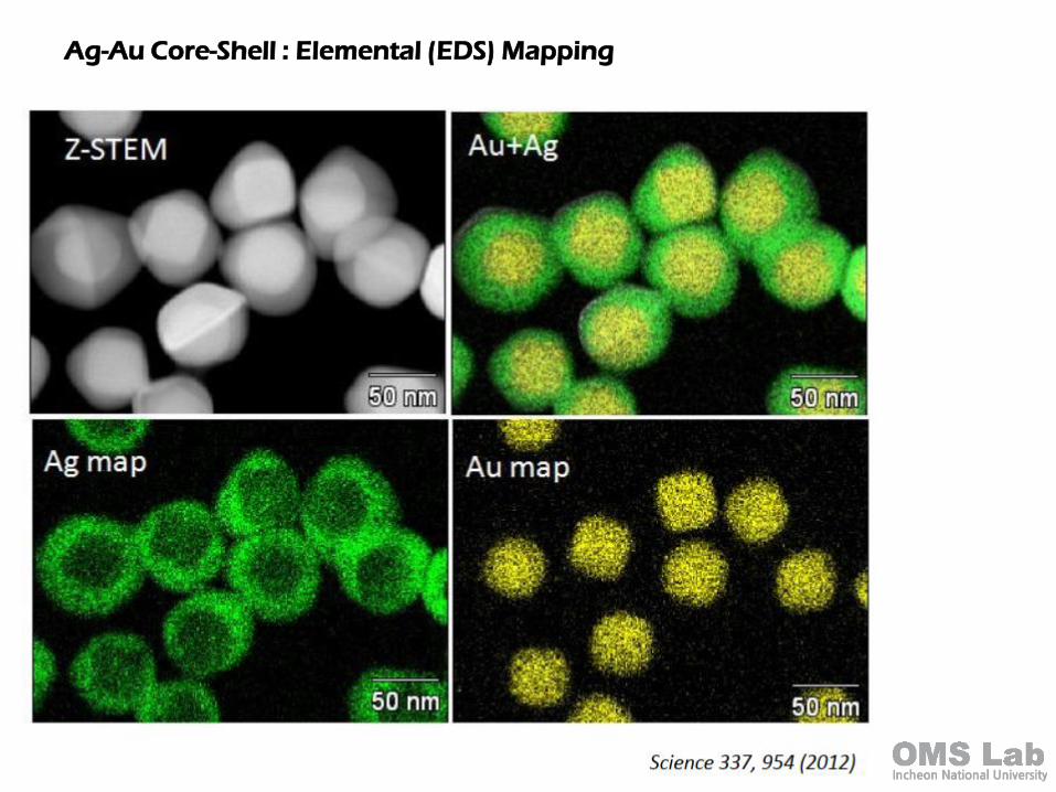
Ag-Au Core-Shell : Elemental (EDS) Mapping
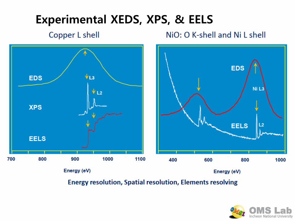
Experimental XEDS, XPS, & EELS
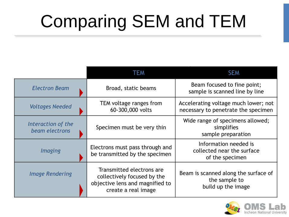
Comparing SEM and TEM
TEM SEM
Imaging Electrons must pass through and
be transmitted by the specimen
Information needed is
collected near the surface
of the specimen
Electron Beam Broad, static beams Beam focused to fine point;
sample is scanned line by line
Voltages Needed TEM voltage ranges from
60-300,000 volts
Accelerating voltage much lower; not
necessary to penetrate the specimen
Image Rendering Transmitted electrons are
collectively focused by the
objective lens and magnified to
create a real image
Beam is scanned along the surface of
the sample to
build up the image
Interaction of the
beam electrons Specimen must be very thin
Wide range of specimens allowed;
simplifies
sample preparation
86
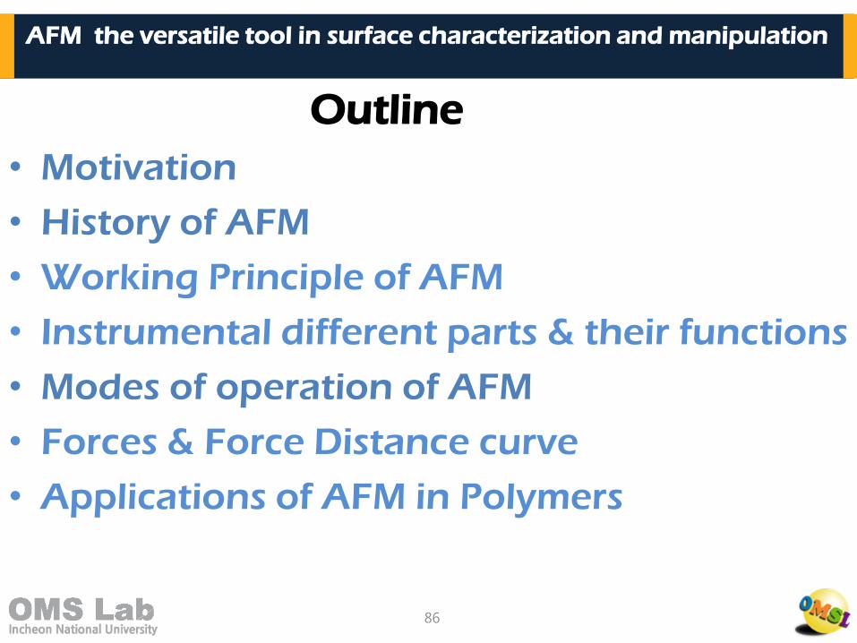
• Motivation
• History of AFM
• Working Principle of AFM
• Instrumental different parts & their functions
• Modes of operation of AFM
• Forces & Force Distance curve
• Applications of AFM in Polymers
AFM the versatile tool in surface characterization and manipulation
Outline
87
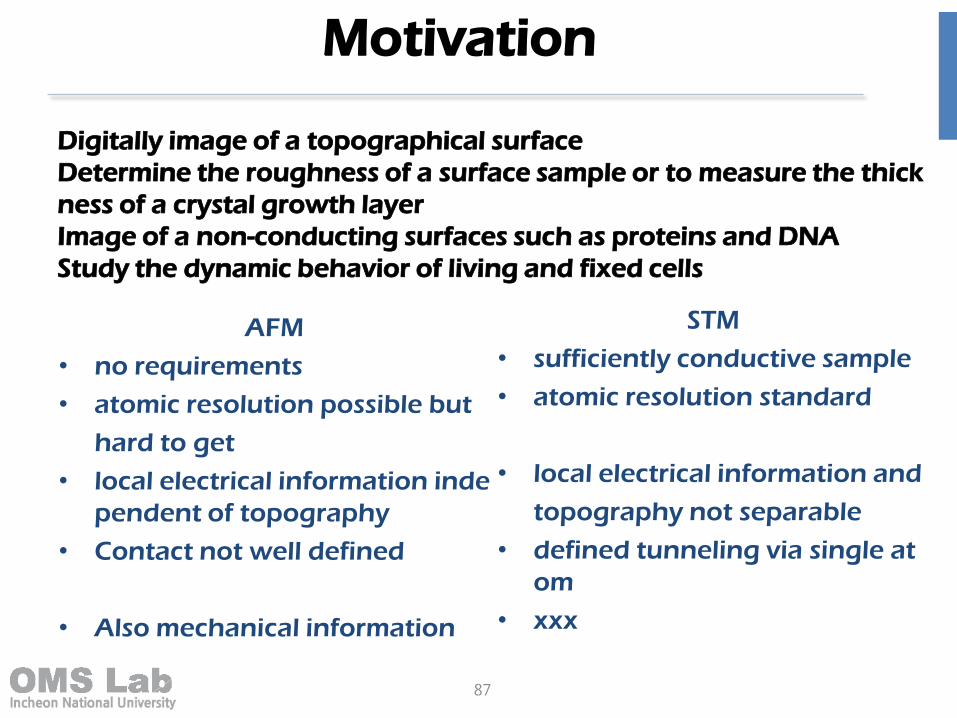
Digitally image of a topographical surface
Determine the roughness of a surface sample or to measure the thick
ness of a crystal growth layer
Image of a non-conducting surfaces such as proteins and DNA
Study the dynamic behavior of living and fixed cells
AFM
• no requirements
• atomic resolution possible but
hard to get
• local electrical information inde
pendent of topography
• Contact not well defined
• Also mechanical information
STM
• sufficiently conductive sample
• atomic resolution standard
• local electrical information and
topography not separable
• defined tunneling via single at
om
• xxx
Motivation
88
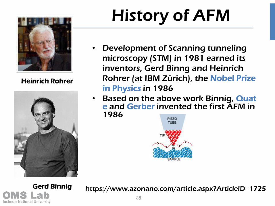
History of AFM
• Development of Scanning tunneling
microscopy (STM) in 1981 earned its
inventors, Gerd Binng and Heinrich
Rohrer (at IBM Zü rich), the Nobel Prize
in Physics in 1986
• Based on the above work Binnig, Quate and Gerber invented the first AFM in 1986
https://www.azonano.com/article.aspx?ArticleID=1725 Gerd Binnig
Heinrich Rohrer
89
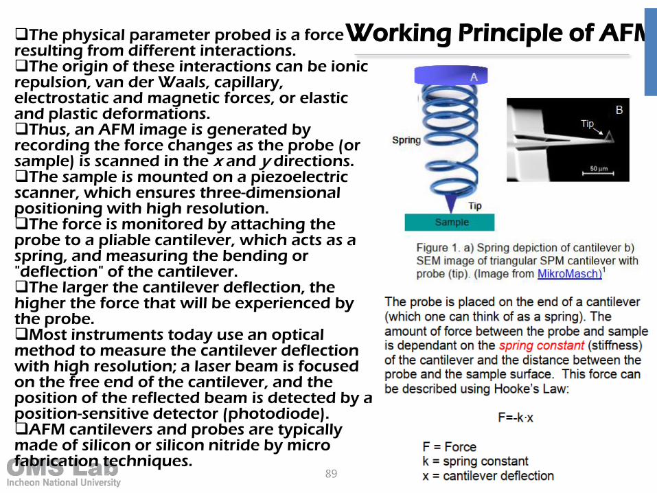
The physical parameter probed is a force resulting from different interactions. The origin of these interactions can be ionic repulsion, van der Waals, capillary, electrostatic and magnetic forces, or elastic and plastic deformations. Thus, an AFM image is generated by recording the force changes as the probe (or sample) is scanned in the x and y directions. The sample is mounted on a piezoelectric scanner, which ensures three-dimensional positioning with high resolution. The force is monitored by attaching the probe to a pliable cantilever, which acts as a spring, and measuring the bending or "deflection" of the cantilever. The larger the cantilever deflection, the higher the force that will be experienced by the probe. Most instruments today use an optical method to measure the cantilever deflection with high resolution; a laser beam is focused on the free end of the cantilever, and the position of the reflected beam is detected by a position-sensitive detector (photodiode). AFM cantilevers and probes are typically made of silicon or silicon nitride by micro fabrication techniques.
Working Principle of AFM
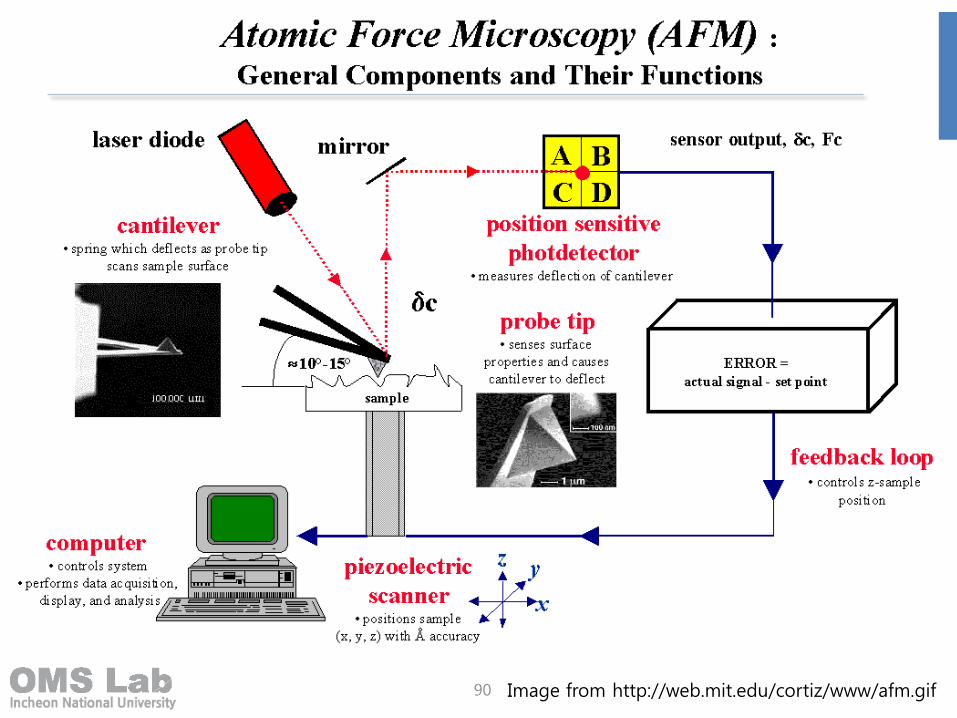
90 Image from http://web.mit.edu/cortiz/www/afm.gif
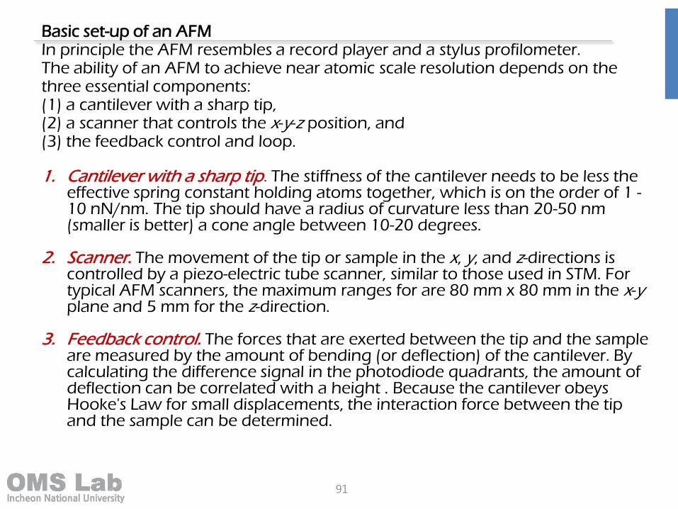
91
Basic set-up of an AFM In principle the AFM resembles a record player and a stylus profilometer. The ability of an AFM to achieve near atomic scale resolution depends on the three essential components: (1) a cantilever with a sharp tip, (2) a scanner that controls the x-y-z position, and (3) the feedback control and loop. 1. Cantilever with a sharp tip. The stiffness of the cantilever needs to be less the
effective spring constant holding atoms together, which is on the order of 1 - 10 nN/nm. The tip should have a radius of curvature less than 20-50 nm (smaller is better) a cone angle between 10-20 degrees.
2. Scanner. The movement of the tip or sample in the x, y, and z-directions is controlled by a piezo-electric tube scanner, similar to those used in STM. For typical AFM scanners, the maximum ranges for are 80 mm x 80 mm in the x-y plane and 5 mm for the z-direction.
3. Feedback control. The forces that are exerted between the tip and the sample are measured by the amount of bending (or deflection) of the cantilever. By calculating the difference signal in the photodiode quadrants, the amount of deflection can be correlated with a height . Because the cantilever obeys Hooke's Law for small displacements, the interaction force between the tip and the sample can be determined.
92
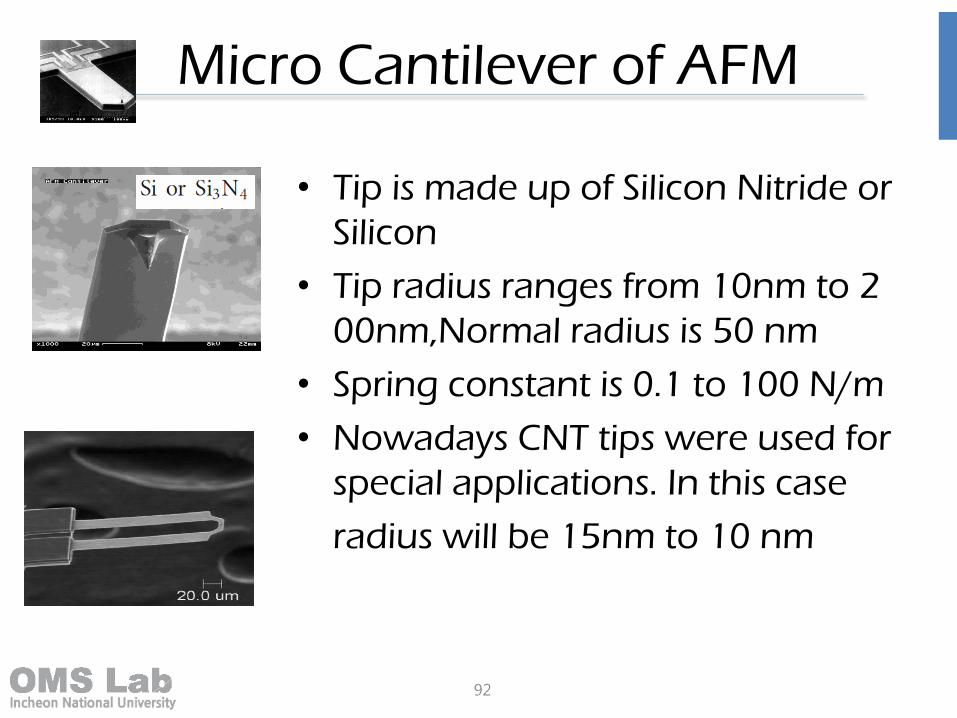
Micro Cantilever of AFM
• Tip is made up of Silicon Nitride or
Silicon
• Tip radius ranges from 10nm to 2
00nm,Normal radius is 50 nm
• Spring constant is 0.1 to 100 N/m
• Nowadays CNT tips were used for
special applications. In this case
radius will be 15nm to 10 nm
93
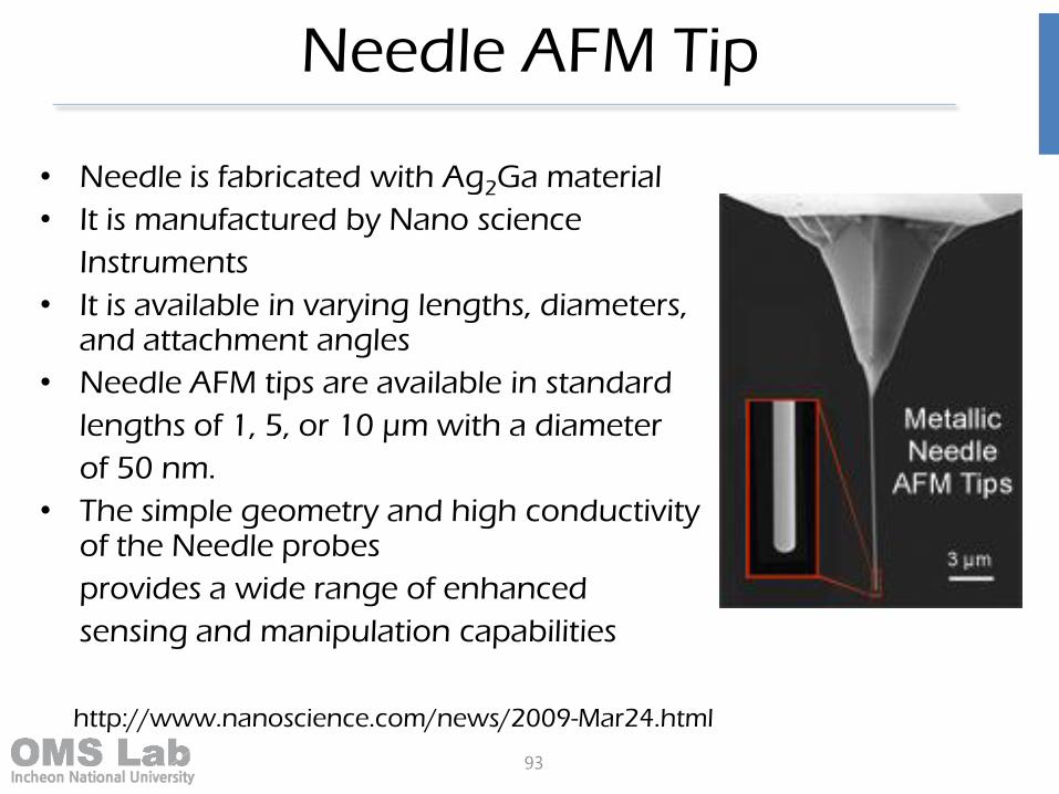
Needle AFM Tip
• Needle is fabricated with Ag2Ga material
• It is manufactured by Nano science
Instruments
• It is available in varying lengths, diameters, and attachment angles
• Needle AFM tips are available in standard
lengths of 1, 5, or 10 µm with a diameter
of 50 nm.
• The simple geometry and high conductivity of the Needle probes
provides a wide range of enhanced
sensing and manipulation capabilities
http://www.nanoscience.com/news/2009-Mar24.html
94
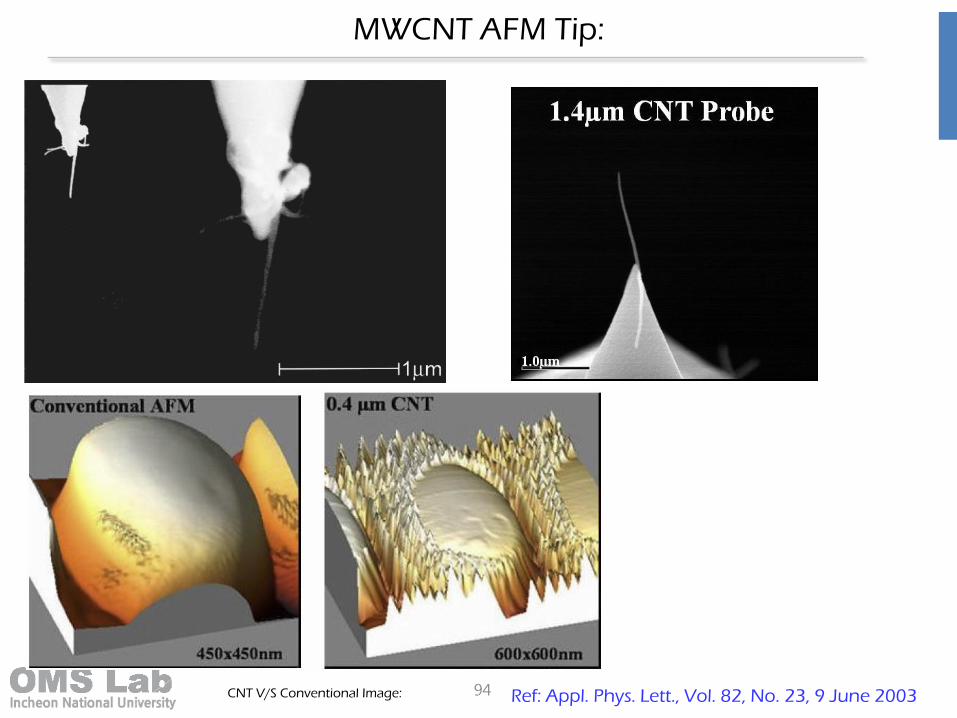
MWCNT AFM Tip:
Ref: Appl. Phys. Lett., Vol. 82, No. 23, 9 June 2003 CNT V/S Conventional Image:
95
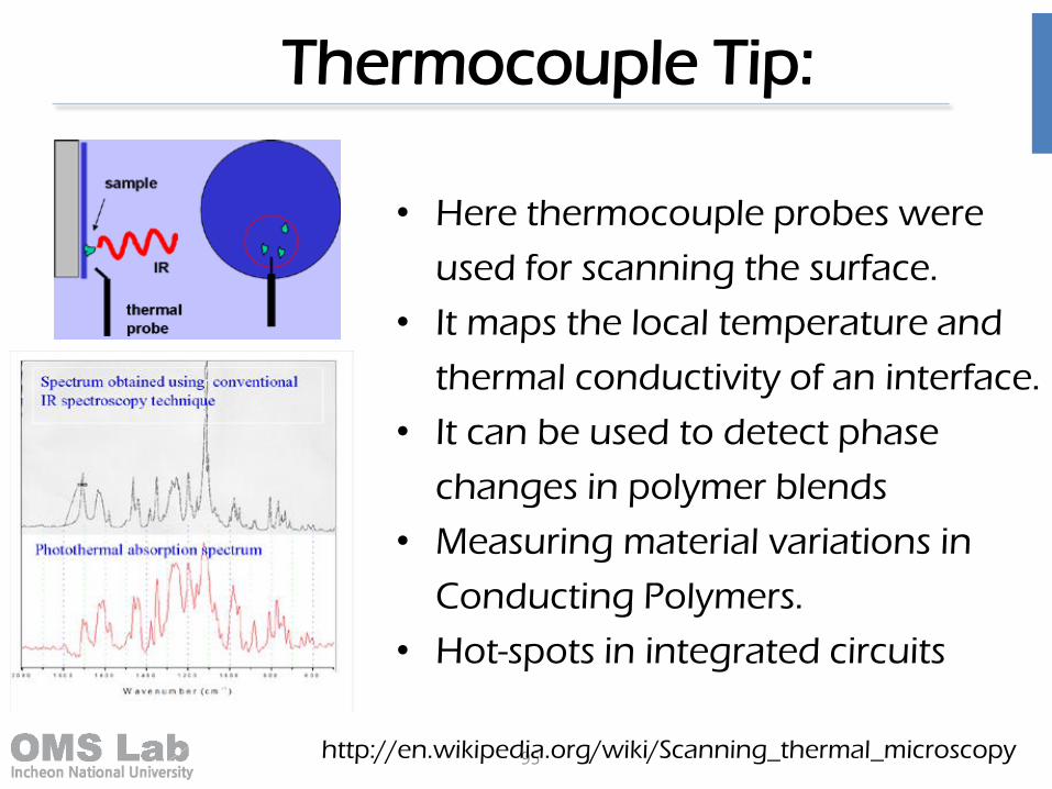
Thermocouple Tip:
• Here thermocouple probes were
used for scanning the surface.
• It maps the local temperature and
thermal conductivity of an interface.
• It can be used to detect phase
changes in polymer blends
• Measuring material variations in
Conducting Polymers.
• Hot-spots in integrated circuits
http://en.wikipedia.org/wiki/Scanning_thermal_microscopy
96
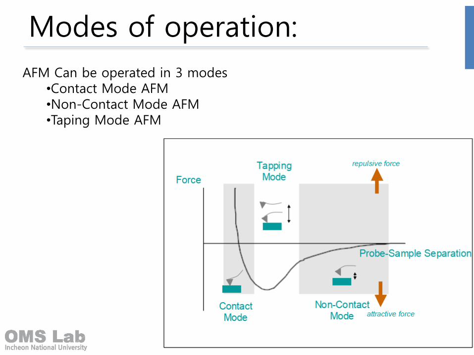
Modes of operation:
AFM Can be operated in 3 modes •Contact Mode AFM •Non-Contact Mode AFM •Taping Mode AFM
97
98
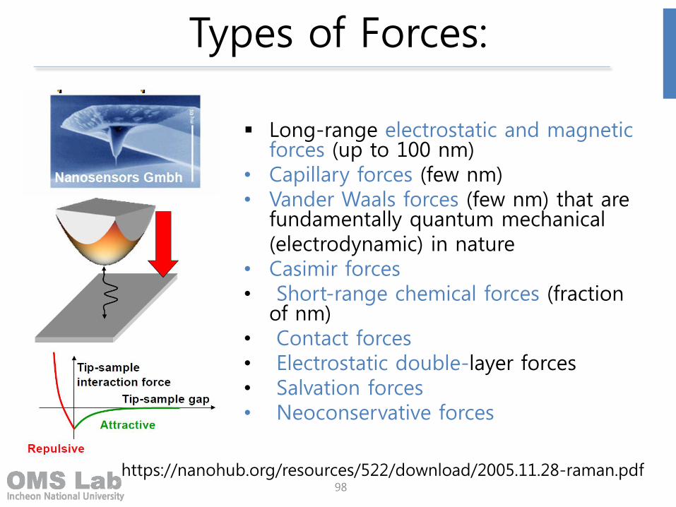
Types of Forces:
Long-range electrostatic and magnetic forces (up to 100 nm)
• Capillary forces (few nm) • Vander Waals forces (few nm) that are
fundamentally quantum mechanical (electrodynamic) in nature • Casimir forces • Short-range chemical forces (fraction
of nm) • Contact forces • Electrostatic double-layer forces • Salvation forces • Neoconservative forces
https://nanohub.org/resources/522/download/2005.11.28-raman.pdf
99
Applications
The AFM is useful for obtaining three-dimensional topographic information of insulating and conducting structures with lateral resolution down to 1.5 nm and vertical resolution down to 0.05 nm. These samples include clusters of atoms and molecules, individual macromolecules, and biologic al species (cells, DNA, proteins). Unlike the preparation of samples for STM imaging, there is minimal sample preparation involved for AFM imaging. Similar to STM operation, the AFM can operate in gas, ambient, and fluid environments and can measure physical properties including elasticity, adhesion, hardness, friction and chemical functionality. A concise applications listing is given below.
I. Metals: tooling studies, roughness measurements, corrosion studies... II. Solid powder catalysts: aggregate structural determination, III. Polymers: determination of morphology and surface properties,
kinetic studies, aging phenomena, surface treatment modifications, adhesion force measurement and indentation,
IV. Biological samples, biomaterials: macromolecules association and conformation studies, adsorption kinetic of molecules on polymer surfaces,
V. Nano- and microparticle structures, Langmuir-Blodgett. Film studies...
101
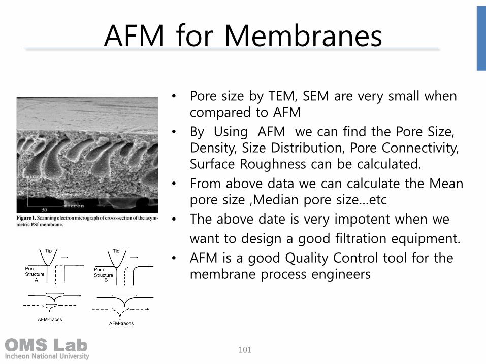
AFM for Membranes
• Pore size by TEM, SEM are very small when compared to AFM
• By Using AFM we can find the Pore Size, Density, Size Distribution, Pore Connectivity, Surface Roughness can be calculated.
• From above data we can calculate the Mean pore size ,Median pore size…etc
• The above date is very impotent when we
want to design a good filtration equipment.
• AFM is a good Quality Control tool for the membrane process engineers
102
103
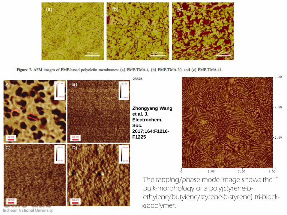
The tapping/phase mode image shows the
bulk-morphology of a poly(styrene-b-
ethylene/butylene/styrene-b-styrene) tri-block-
copolymer.
Zhongyang Wang
et al. J.
Electrochem.
Soc.
2017;164:F1216-
F1225
104
105
Advantages
The AFM has several advantages over the scanning electron microscope (SEM). Unlike the electron microscope AFM provides a true three-dimensional surface profile. Samples viewed by AFM do not require any special treatments (such as metal/carbon coatings) that would irreversibly change or damage the sample. While an electron microscope needs an expensive vacuum environment for proper operation, most AFM modes can work perfectly well in ambient air or even a liquid. Possible to study biological macromolecules and even living organisms. In principle, AFM can provide higher resolution than SEM. It has been shown to give true atomic resolution in ultra-high vacuum (UHV).
Disadvantages
A disadvantage of AFM compared with the scanning electron microscope (SEM) is the image size. The SEM can image an area on the order of millimeters by millimetres with a depth of field on the order of millimetres. The AFM can only image a maximum height on the order of micrometres and a maximum scanning area of around 150 by 150 micrometres. Another inconvenience is that at high resolution, the quality of an image is limited by the radius of curvature of the probe tip, and an incorrect choice of tip for the required resolution can lead to image artifacts. Traditionally the AFM could not scan images as fast as an SEM, requiring several minutes for a typical scan, while an SEM is capable of scanning at near real-time (although at relatively low quality) after the chamber is evacuated. AFM images can be affected by hysteresis of the piezoelectric material .
106
References: • Polymer Microscopy By Linda C. Sawyer, David T.Grubb
• Synthetic Polymeric Membranes By K.C.Khulbe, C.Y.Feng, T.Matsuura
• Atomic Force Microscopy in Cell Biology By Bhanu P.Jena, J.K.heinrich Horber,
American Society for Cell Biology
• Atomic Force Microscopy By Pier Carlo Braga, Davide Ricci
• Ref: Appl. Phys. Lett., Vol. 82, No. 23, 9 June 2003
• M. R. VanLandingham, J. S. Villarrubia, W. F. Guthrie, G. F. Meyers, "Nanoindentation of Polymers: An Overview," in Macromolecular Symposia, 167,
• Advances in Scanning Probe Microscopy of Polymers, V. V. Tsukruk and N. D. Spencer, eds. (2001) 15-44.
• Miscibility of Branched Ethene Homopolymers with Iso- and Syndiotactic Polypropenes. Jürgen Marquardt, Ralf Thomann, Yi Thomann, Johannes Heinemann and Rolf Mülhaupt Macromolecules, 2001, 34, (25), 8669-8674
• Macromolecular Materials and Engineering (2008), 293(3), 218-227.
• Microsc Microanal 10(Suppl 2), 2004
• Appl. Phys. Lett., Vol. 82, No. 23, 9 June 2003
• www.nanoscience.com/news
• www.wikipedia.org
• www.google.com
• www.nanohub.com/online_onlinelectures