Embed Size (px)
Citation preview

www.technology.matthey.comJOHNSON MATTHEY TECHNOLOGY REVIEW
http://dx.doi.org/10.1595/205651316X691186 Johnson Matthey Technol. Rev., 2016, 60, (2), 117–131
117 © 2016 Johnson Matthey
The Use of Annular Dark-Field Scanning Transmission Electron Microscopy for Quantitative CharacterisationA review of techniques developed for a high resolution study of bimetallic catalysts and other materials
By Katherine E. MacArthur*§
University of OxfordParks Road, Oxford OX1 3PH, UK
*Email: [email protected]
§Present address: Ernst Ruska Centrum, Forschungszentrum Jülich GmbH, 52425 Jülich, Germany
Small metallic nanoparticles used for polymer exchange membrane fuel cells (PEMFC) represent a characterisation challenge. Electron microscopy would seem the ideal technique to analyse their structure at high resolution. However, their minute size and sensitivity to irradiation damage makes this diffi cult. In this review, the latest techniques for overcoming these limitations in order to provide quantitative structural and compositional information are presented, focusing specifi cally on quantitative annular dark-fi eld (ADF) scanning transmission electron microscopy (STEM) and quantitative energy dispersive X-ray (EDX) analysis. The implications for the study of bimetallic fuel cell catalyst materials are also discussed.
1. Introduction
It is well established that catalyst nanoparticles are critical to the success of PEMFC; indeed it is
the cost of the platinum loading which currently limits their wide-scale use. To help the search for better catalysts, with higher catalytic activity and specifi city and lower cost, steady improvement in characterisation abilities is essential. Since the technique’s infancy (1), ADF STEM has been utilised for the study of catalysts due to the strong dependence of signal intensity on atomic number (see Figure 1). This so-called ‘Z-contrast’ has enabled differentiation of individual heavy atoms from lighter, and even crystalline, supports well before atomic resolution was even possible, as fi rst demonstrated by Crewe, Wall and Langmore (1) and later by Nellist and Pennycook (2) among others. STEM suffers from the inherent problem of many other high resolution techniques, where the particularly small area investigated may not be representational of the whole sample. However the technique does provide the local atomic scale information which is essential to completely understand catalysts at the same length scales as their chemical reactions.
This paper will introduce the key advantages and limitations of STEM for materials characterisation. Some of the more recent advances and developments in the fi eld of quantifi cation, where the machines are beginning to be used much more as analytical tools rather than high resolution cameras, will also be discussed.

118 © 2016 Johnson Matthey
http://dx.doi.org/10.1595/205651316X691186 Johnson Matthey Technol. Rev., 2016, 60, (2)
2. The Fundamentals of Scanning Transmission Electron MicroscopySTEM is a process where pre-specimen lenses focus the beam into a small probe that is scanned in a raster pattern across the sample (see Figure 2(a)). This is
similar to scanning electron microscopy (SEM) (3) except that here the transmission signal is collected and it is customary to use an electron transparent transmission electron microscopy (TEM) thin foil, producing signifi cantly improved resolution because beam-spreading or particle scattering events are reduced in thin samples. There are a variety of signals emitted by the sample due to excitation from the high energy electron probe (see Figure 2(b)). One of the major advantages of STEM is the ability to detect several of these signals in parallel. The collection of several signals in parallel is particularly benefi cial for beam sensitive samples, such as catalysts, as they will often damage or reconstruct during analysis due to the high energy provided by the electron beam. This means that sequential images will not present the same sample structure, especially at atomic resolution.
A small on-axis detector, with an outer collection angle typically less than 5 mrad, produces a bright-fi eld (BF) STEM image. The origin of the image contrast is the interference between overlapping Bragg disks (these disks are green in Figure 2(a)). Due to the theory of reciprocity (5) BF-STEM, with a convergent illumination and a small on-axis detector, is analogous to BF high resolution TEM, with a small point source and a large detector collecting the resultant scattered beams. A disadvantage of both methods is that they suffer contrast inversions with defocus and thickness, and
20 nm
Fig. 1. Example of a low magnifi cation ADF STEM image of Pt(Pd) core-shell catalyst nanoparticles which show up much more brightly than the low atomic number carbon black support. Image was taken on a Jeol atomic resolution microscope (ARM)
Electron sourceObjective aperture
Objective lens
Focused probe at specimen
ADF detectorBright fi eld detector
Incident high-kV beam Secondary
electrons (SE)Characteristic X-rays
Visible light
Electron-hole pairs
Bremsstrahlung X-rays
Inelastically scattered electronsDirect
beam
Elastically scattered electrons
Specimen
‘Absorbed’ electrons
Auger electrons
Backscattered electrons (BSE)
Fig. 2. (a) Schematic of i mage formation in a STEM, showing the on-axis small bright-fi eld detector and the larger annular dark-fi eld detector, pink; (b) signals generated when a high-energy beam of electrons interacts with a thin specimen. The directions shown for each signal do not always represent the physical direction of the signal but indicate, in a relative manner, where the signal is the strongest or where it is detected. Image (b) was redrawn from Williams and Carter (4)
(a) (b)
Overlapping Bragg discs

119 © 2016 Johnson Matthey
http://dx.doi.org/10.1595/205651316X691186 Johnson Matthey Technol. Rev., 2016, 60, (2)
diffi culties associated with image interpretation of a coherent signal (4). A recent approach aims to produce a more incoherent BF image by using an annular detector, referred to as annular bright-fi eld (ABF). The theory is that ABF is more sensitive to lighter elements like oxygen or lithium (6–8), although the exact origin of the image contrast is still a matter of debate so whether or not quantitative intensity information can be extracted is uncertain.
Using an annular detector to only collect the electrons scattered to higher angles, typically larger than 80 mrad, often referred to as high angle annular dark-fi eld (HAADF), produces a coherency loss in the signal detected. Originally, Howie proposed (9) that the cause of this coherency loss was thermal diffuse scattering (TDS) at larger detector angles becoming the more dominant scattering mechanism over elastic or Bragg scattering. However, it was later demonstrated that the process of integration of the signal over a large annular detector, and therefore a large range of scattering angles, is the cause of the coherency loss. Any dynamical elastic diffraction of electrons scattered onto the detector will have no effect on the fi nal image as the intensity is only redistributed elsewhere in the detector and is still integrated into the total collected signal (10). ADF STEM produces an image with atomic number sensitivity or Z-contrast following power law relationship Zα, where α is between 1 and 2 depending on the angular range of electrons collected (11) and relative Debye-Waller factor between atoms among other things. Many early attempts at intensity quantifi cation have relied on accurately characterising this exponent.
2.1 Aberration Correction
Unlike optical lenses, electromagnetic lenses contain inherent aberrations that are unavoidable (4, 12, 13). When aberration correction is discussed it normally refers to correction of the positive spherical aberration, Cs or C3, in which the rays furthest from the optic axis are focused more by the lens fi eld. In early instrumentation, namely TEM, resolution was improved by using higher accelerating voltages (14) in order to minimise the sample interaction volume, a process which inevitably had its own limitations due to the resulting high damage rates. Later it was combatted by using a so-called high-resolution or narrow gap pole piece with a much smaller Cs of 0.7 mm (15). However, the narrow gap produces large restrictions on specimen holders, including tilt ranges and in situ cells and limits
the possible additional detectors for microanalysis. The most recent solution is an aberration corrector, where a series of non-round lenses are used to counteract the aberrations, similar to the lenses in glasses for eyesight improvement. In STEM this results in not only a reduced probe size (improving resolution) but also an increase in the current density within this corrected probe (16), causing an enhanced signal-to-noise ratio (SNR) during imaging and signifi cant improvement in counts for microanalysis. Aberration correctors allow microscopes to keep their large pole piece gaps and are now commercially available, existing in microscopes around the world (16–19).
3. Quantifi cation of Annular Dark-Field Images
ADF STEM images are easy to interpret qualitatively due to the Z-contrast nature of the technique and the absence of any contrast inversions with thickness. The information they can provide when images are treated as data sets and analysed quantitatively is only just beginning to be explored. Often what people mean by ‘quantifi cation’ is a comparison with simulated images. Anderson et al. (20) scaled simulated images to fi t with experimental data rather than acquire them on an absolute scale. Darji and Howie (21) have also discussed the necessity of correcting experimental data; in this case for additional scattering from a crystalline substrate, as they believed this was the origin of the mismatch between experiment and simulation. Meanwhile for TEM there is a widely accepted mismatch between simulation and experimental intensity known as the Stobbs factor (22).
The earliest attempts on quantifi cation were by Retsky (23) and Isaacson et al. (24) in the 1970s, comparing the integrated intensity of heavy metal atoms or small clusters to those values calculated from fi rst principle quantum mechanics. Work on small metallic clusters has often assumed that the integrated ADF intensity of a cluster scales linearly with the number of atoms it contains (25, 26). Therefore if the intensity of a single atom is known, dividing the total intensity of a cluster by this value yields the cluster size in atoms. It is an acceptable approximation for amorphous and off-axis clusters where it can be assumed that no channelling (see below) is occurring. However, it is overly simplistic to assume such linearity for on-axis crystalline particles and neglecting coherency effects in calculations is likely to cause signifi cant errors.
120 © 2016 Johnson Matthey
http://dx.doi.org/10.1595/205651316X691186 Johnson Matthey Technol. Rev., 2016, 60, (2)
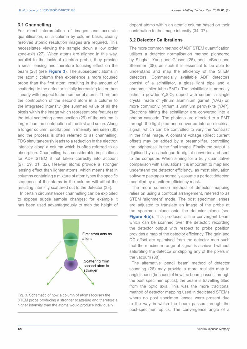
3.1 Channell ingFor direct interpretation of images and accurate quantifi cation, on a column by column basis, cleanly resolved atomic resolution images are required. This necessitates viewing the sample down a low order zone-axis (27). When atoms are aligned in this way, parallel to the incident electron probe, they provide a small lensing and therefore focusing effect on the beam (28) (see Figure 3). The subsequent atoms in the atomic column then experience a more focused probe than the fi rst atom; resulting in the amount of scattering to the detector initially increasing faster than linearly with respect to the number of atoms. Therefore the contribution of the second atom in a column to the integrated intensity (the summed value of all the pixels within the image which represent one feature) or the total scattering cross section (29) of the column is larger than the contribution of the fi rst and so on. Along a longer column, oscillations in intensity are seen (30) and the process is often referred to as channelling. TDS simultaneously leads to a reduction in the electron intensity along a column which is often referred to as absorption. Channelling has considerable implications for ADF STEM if not taken correctly into account (27, 29, 31, 32). Heavier atoms provide a stronger lensing effect than lighter atoms, which means that in columns containing a mixture of atom types the specifi c sequence of the atoms in the column will affect the resulting intensity scattered out to the detector (33).
In certain circumstances channelling can be exploited to expose subtle sample changes; for example it has been used advantageously to map the height of
dopant atoms within an atomic column based on their contribution to the image intensity (34–37).
3.2 Dete ctor Calibrations
The more common method of ADF STEM quantifi cation utilises a detector normalisation method pioneered by Singhal, Yang and Gibson (26), and LeBeau and Stemmer (38), as such it is essential to be able to understand and map the effi ciency of the STEM detectors. Commercially available ADF detectors consist of a scintillator, a glass light pipe and a photomultiplier tube (PMT). The scintillator is normally either a powder Y2SiO5 doped with cerium, a single crystal made of yttrium aluminium garnet (YAG) or, more commonly, yttrium aluminium perovskite (YAP). Electrons hitting the scintillator are converted into a photon cascade. The photons are directed to a PMT through the light pipe and converted into an electrical signal, which can be controlled to vary the ‘contrast’ in the fi nal image. A constant voltage (direct current offset) may be added by a preamplifi er, controlling the ‘brightness’ in the fi nal image. Finally the output is digitised by an analogue to digital converter and sent to the computer. When aiming for a truly quantitative comparison with simulations it is important to map and understand the detector effi ciency, as most simulation software packages normally assume a perfect detector, modelled by a uniform effi ciency mask.
The more common method of detector mapping relies on using a confocal arrangement, referred to as STEM ‘alignment’ mode. The post specimen lenses are adjusted to translate an image of the probe at the specimen plane onto the detector plane (see Figure 4(b)). This produces a fi ne convergent beam which can be scanned over the detector; recording the detector output with respect to probe position provides a map of the detector effi ciency. The gain and DC offset are optimised from the detector map such that the maximum range of signal is achieved without saturating the detector or clipping any of the pixels in the vacuum (38).
The alternative ‘pencil beam’ method of detector scanning (26) may provide a more realistic map in angle space (because of how the beam passes through the post specimen optics); the beam is travelling tilted from the optic axis. This was the more traditional method of detector mapping used in dedicated STEMs where no post specimen lenses were present due to the way in which the beam passes through the post-specimen optics. The convergence angle of a
First atom acts as a lens
Scattering from second atom is stronger
Fig. 3. Schematic of how a colu mn of atoms focuses the STEM probe producing a stronger scattering and therefore a higher intensity than the atoms would produce individually

121 © 2016 Johnson Matthey
http://dx.doi.org/10.1595/205651316X691186 Johnson Matthey Technol. Rev., 2016, 60, (2)
typical STEM probe is around 20 mrad, whereas the angle of scattering out to the detector can be up to ten times that. These scattered electrons will interact with post specimen lenses at a very large tilted angle where lens aberrations are normally worse, making it benefi cial to map the detector in angle space. However, it is more diffi cult to set up and thus its use so far has been limited to dedicated STEM machines.
When using detector normalisation for quantitative analysis it is important to be aware of the linearity of the detector response (38–40). In particular, altering the detector contrast does not produce a linear variation (41) in the detector signal, which is why contrast and brightness settings are normally kept constant between detector mapping and experimental images.
The majority of image intensity detector normalisation methods rely on the detector responding linearly with the number of incident electrons. Care should be taken not to rely too heavily on this linearity alone. During experimental image acquisition the detector will see a diffuse electron fl ux (see Figure 4(a)) at a much lower intensity, whereas during detector mapping the whole beam is scanned over it in a fi ne probe. To combat this it is prudent to drop the probe current by a known amount during the detector mapping (42) and subsequently incorporate a ratio of the probe currents into the quantifi cation method. Lowering the current also helps to minimise damage to the detector and makes a greater contrast range available in the fi nal experimental image, which is particularly useful
for imaging nanoparticles or other low dimensional materials.
Working from the premise that real detectors are asymmetric in their collection effi ciency (43, 44) there needs to be a way to compensate for this to improve matching with simulations. Rosenauer et al. (39) use a two-dimensional (2D) profi le estimate of their detector asymmetry to simulate images with an asymmetric detector; however this approach is only possible with certain simulation packages. The fl ux weighting method developed by Martinez et al. (45) aims to improve the detector normalisation by accommodating for this asymmetry in the experimental images rather than adjusting the simulations.
3.3 Recent Advances in STEM Quantifi cation
LeBeau and Stemmer are generally acknowledged as the originators of a resurgence of interest in detector calibrations and recording images on an absolute intensity scale (see Figure 5) (38). Their method relies on a full characterisation of microscope imaging parameters and detector responses in order to achieve direct comparison with simulations (46), although defocus has been fi tted empirically from selecting the simulated image which fi ts most closely to experimental images.
Quantitative comparison between experiment and simulation has only become possible due to improvements in parallelisation of simulation software, fi rst on central processing units (CPU) and then graphical processing units (GPU). Such parallelisation makes it possible to produce accurate simulation reference libraries in reasonable time-scales using the more accurate (but more computer intensive) frozen phonon approach rather than absorptive potential (47).
From a detector effi ciency map like the one presented in Figure 6(b), the average pixel intensity in the active region (the area coated with the scintillator, predominantly blue in Figure 5(b)) can be considered to represent one hundred percent of the total electron beam, whilst the average intensity of the background region (anywhere in the image detector image considered not to be the active region) represents no-beam and is also known as the black-level. Normalising experimental images using these maps results in images being scaled as a fraction of the incident beam which has been scattered out to the detector.
An improvement to this has been developed by calculating the scattering cross-section (29) or
(a) (b)
Fig. 4. (a) Ray diagram of a STEM with the electron fl ux seen by the detector due to scattering from the sample; (b) scanning confocal geometry where the image of the probe at the specimen plane is transferred to the detector plane

122 © 2016 Johnson Matthey
http://dx.doi.org/10.1595/205651316X691186 Johnson Matthey Technol. Rev., 2016, 60, (2)
Gaussian volume (31, 48) of each atomic column within an image. Scattering cross-sections are calculated by integrating the normalised intensity over one atomic column, using a Voronoi polygon (49, 50) or otherwise, and multiplying by pixel area. This creates a value with area units that represents the probability
of electrons interacting with that column and scattering out to the ADF detector, much in the way that other cross-sections behave in particle physics. Gaussian volumes are mathematically identical to cross-sections (51), only instead of integrating the intensity in a polygon method, a 2D Gaussian curve is fi tted to the
(a) (b)
0 2 4 6 8 10 12 14 16 18Percentage of incident probe intensity
0.5 nm
Fraction of average intensity 0 0.2 0.4 0.6 0.8 1.0 1.2
Fig. 5. (a) One of the fi r st ADF STEM images normalised to the incident beam. The sample is a gold wedge and the white numbers represent the assigned atom counts based on direct comparison with simulation; (b) the associated detector effi ciency map in units of fraction of the average intensity of the active region. (Reprinted with permission from (46). Copyright (2010) American Chemical Society)
100 200 300 400 500 600 700 800 0 5 10 15 Scattered intensities, au Number of Gaussians
9
8
7
6
5
4
3
2
1
0
Freq
uenc
y
ICL
crite
rion
1870
1850
1830
(a) (b) (c)
Fig. 6. (a) Image of a sil ver nanoparticle embedded in an aluminium matrix, the dots represent the estimated position of the atomic columns with those assigned as silver marked in red; (b) histogram of the scattered intensities of the Ag columns. The black solid curve shows the estimated mixture model; the individual components are shown as dashed curves; (c) the ICL criterion evaluated as a function of the number of Gaussians in a mixture model. The minimum at 10 components represents the optimum number of components (Reprinted by permission from Macmillan Publishers Ltd: Nature (59), copyright (2011))

123 © 2016 Johnson Matthey
http://dx.doi.org/10.1595/205651316X691186 Johnson Matthey Technol. Rev., 2016, 60, (2)
image intensity of each column and the integrated volume under this curve is used. Using these volumes or cross-sections for quantifi cation still requires comparison with simulations but is a lot more robust to defocus, tilt, source size and other aberrations (29, 32, 48). Although the robustness of such an integration or averaging over a unit cell has been commented on before (20, 39, 52), it was not until the scattering cross-section work (29, 32, 48, 51) that it was mathematically proven and robustly tested through a series of simulations. Scanning distortions may still affect the quantifi cation accuracy; recent advances in non-rigid image registration may provide the solution to this (53–55).
An alternative technique to direct comparison with simulation is one based on statistical parameter estimation theory (56), pioneered by Van Aert et al. (57). The theory relies on the inherently quantised nature of a histogram of integrated intensities from an experimental image (58). For a single element scenario, for example the silver particle in Figure 6, the integrated intensities should naturally be quantised in the histogram due to the fact that each column contains an integer number of atoms. These discrete values become somewhat smeared by Poisson noise and other random errors; however, it should still be possible to decompose the histogram of all the integrated intensities into a series of Gaussian components through statistical estimation and a maximum likelihood criterion. The critical component of this algorithm is a ‘cost function’ to minimise the total number of Gaussians incorporated, otherwise the best solution would be an infi nite number of Gaussians. The integrated classifi cation likelihood (ICL) criterion is used for this purpose and provides a local minimum at the optimum number of components (Figure 4(c)).
The main advantage of ICL is that it does not require the experimental images to be intensity normalised. A systematic error or scaling can easily be incorporated or alternatively it can be used as an independent method of atom counting. The limitations of the ICL approach have also been covered by Van Aert (51) and De Backer et al. (60). In particular the fi eld of view and therefore the number of observations per Gaussian component greatly affect the ability of the ICL criterion to estimate the correct number of components. This is critical for investigations of nanomaterials where their fi nite size severely limits the number of observations available per component, but could potentially be overcome by
combining several images for incorporation into the histogram (31).
3.4 Three-Dimensional Reconstruction
The traditional method for three-dimensional (3D) reconstruction is electron tomography (61), developed from X-ray tomography (62). A 3D structure is reconstructed from a tilt series of images using one of a variety of possible reconstruction algorithms (63, 64). The main requirement is for the micrographs to be ‘true projections of the structure’ (65) such that image intensities are a monotonic function of sample thickness. Therefore the use of TEM or BF-STEM is not desirable because Fresnel fringes and diffraction contrast are a signifi cant problem. Tomography was initially developed for biological samples (66, 67) and is regularly used to determine the location of catalysts particles on their supports (68–73). Once the 3D shape has been reconstructed important information such as surface area, volume and thickness distributions can be measured for particles (74). Carrying out tomographic reconstructions by this method subjects the sample to high amounts of electron dose from the hundred images required for a single reconstruction and the dose infl icted during any tilting and re-centring processes between frames.
The more recent method of discrete tomography (75) signifi cantly reduces the number of necessary projections to less than 10, even in the presence of noise or defects, through the use of ‘prior knowledge’. Atomic resolution discrete tomography (59) uses the prior knowledge that the particles have crystalline structure, contain no voids and surface steps and kinks are minimised. This is primarily carried out by defi ning each crystallographic point as a boxed region and then only one atom may lie within each box.
Van Aert et al. were the fi rst group to publish atomic resolution discrete tomography data on their embedded silver nanoparticle (59) and also the core of core-shell semi-conductor nanocrystals (76). In their research they found that two or three quantifi ed HAADF STEM images down crystallographic orientations (for example [100], [010] and [110]) gave suffi cient information to reconstruct the particle, provided the atoms are restricted to a particular, in this case face-centred cubic (fcc), crystalline structure. Their quantitative STEM method (57) was used on each projection image to estimate the number of atoms before carrying out a reconstruction. It is, however, important to note that both of the example particles used to demonstrate this method had been

124 © 2016 Johnson Matthey
http://dx.doi.org/10.1595/205651316X691186 Johnson Matthey Technol. Rev., 2016, 60, (2)
embedded in another material, thereby limiting the surface mobility and improving the dose tolerance for such reconstructions to be carried out.
A more recent alternative to tomography has been designed specifi cally for the study of free standing catalysts where the mobility of surface atoms between sequential images will be high. Using the method of quantitative STEM with scattering cross-sections, an automated procedure has been developed for peak fi nding (to fi nd each atomic column location within an image) and subsequently estimating the number of atoms they contain (77). Armed with the atomic column locations and the number of atoms it becomes possible to estimate the 3D structure from only one experimental image (see Figure 7). The same assumptions described above for atomic resolution discrete tomography are combined with atomic spacing in the beam direction predicted from bulk crystal
information. A signifi cant advantage to this approach is the requirement of only one experimental image for 3D information. This not only provides reduced dose capabilities but also increases throughput, leading to the ability to reconstruct a time series of images (77) or several particles in one sample (47, 78).
4. Composition Analysis
The STEM image intensity contains both composition and thickness information which can be diffi cult to differentiate. A particular example of this is acid leached platinum cobalt nanoparticles; the increased ADF image intensity of the heavy metal shell is swamped by the loss in intensity due to the large reduction in sample thickness at the particle surface (79, 80). The challenge facing quantifi cation of bimetallic systems is how to incorporate additional
0.02 0.06 0.1 0.14 0 10 20 30 40 Fraction of incident beam Scattering cross section, Mb
(a) (b)
Fig. 7. Particle 3 – norma lised experimental ADF image (a) of a Pt/Ir particle with the calculated cross-section map; (b) the 3D reconstructed particle is shown parallel to the beam direction; (c) perpendicular to the beam direction at from two angles 90º from each other (d) and (e). For ease of comparison with a Wulff construction the (d) projection has had the faces coloured in, {111} purple, {100} blue, {110} red
(c) (d) (e)

125 © 2016 Johnson Matthey
http://dx.doi.org/10.1595/205651316X691186 Johnson Matthey Technol. Rev., 2016, 60, (2)
information or assumptions in order to separate out the thickness and composition contributions from the ADF STEM signal. For PEMFCs in particular it is desirable to understand how much Pt there is and its location on the particle surfaces.
A combination of sequential high resolution STEM images and multi-slice simulation has been successfully implemented by Ortalan et al. (81) on iridium-rhodium clusters, using intensity ratios to predict possible combinations of Ir and Rh in each column. This procedure, however, was only possible due to the small size of the clusters investigated (containing a maximum of three atoms per column); at larger particle sizes with an exponential increase in the number of possible combinations this approach quickly becomes unrealistic. Carlino and Grillo (82, 83) demonstrated that it is possible to use a section of sample with known composition to interpolate the thickness where composition is unknown to estimate composition changes on a relative scale. Rosenauer et al. have extended this approach at atomic resolution analysis (49, 84). However, this technique is rather limited to the semiconductor multilayer systems for which it was designed, where areas of known composition are present in the same image. Molina (85, 86) and Hernández-Maldonado et al. (87) have demonstrated approaches using a series of carefully controlled reference samples with accurately known composition, although this comes with its own problems of being able to manufacture such standards.
With these restrictions to quantitative ADF STEM for compositional analysis it is therefore useful to look at the other available signals which an electron microscope can provide. Elemental analysis of catalyst particles began as early as 1983 (88). The advantage of using so-called microanalysis in the electron microscope is the ability to achieve compositional information at the same length scale as the electron micrographs thereby providing invaluable local microstructural information of a sample. Here the focus is on EDX, one of the two microanalysis techniques which can be carried out within a TEM/STEM. EDX analysis relies on the excitation and ejection of an inner shell electron within an atom in the sample. An outer shell electron fi lls the subsequent hole whilst emitting an X-ray of characteristic energy. The EDX signal has signifi cantly worse SNR than ADF but the elemental information is much more readily separable. The alternative technique, electron energy loss spectroscopy (EELS), provides higher count rates but in many cases can
prove challenging to use for mapping of several elements at the same time. This is especially true for heavy elements like Pt (89) where the ionisation edge is very high energy. Microanalysis is a region where STEM demonstrates advantages over TEM due to the focused probe providing localised information and the ability to collect ADF and microanalysis signals simultaneously.
Aberration correction has produced a signifi cant advancement for microanalysis, particularly in the realms of 2D elemental mapping due to the signifi cant increase in current density within the fi ner corrected probe. However for samples prone to beam damage this high current density is a problem. For mapping in particular, one must be aware of the damage being caused by the long acquisition times in order to improve total counts (90). From experience (47) it has been found that this damage can be minimised through using sequential fast scanning, where several fast acquisitions of a line scan or map are combined, to reduce the dwell time per pixel per scan while still maintaining the total live time necessary for high counts. Ideally sub-pixel scanning is also used so the beam is never stationary over the sample. It is unclear why such an approach yields lower damage unless the lower dose rate per pixel allows suffi cient time for the charge or heat to dissipate away from the analysis region into the remainder of the sample.
Even without aberration correction Prestvik et al. carried out some of the earliest investigations into STEM-EDX analysis of bimetallic nanoparticles where individual platinum-rhenium particles sized 0.5–2.5 nm were imaged and the percentage Pt was plotted against particle size (91). EDX mapping has been used to demonstrate the localisation of sulfur on the nanoparticles in ‘poisoned’ catalysts (90). In more recent years EDX of 5 nm core-shell nanoparticles mapping has been able to differentiate the layered structure very effectively (89); however the atomic columns are not resolved due to the trade-off between resolution and counts. Deepak et al. (89) have demonstrated the use of multivariate statistical analysis (92) to improve their quantifi cation, mining their data cube for independently varying compositions.
The new generation of EDX detectors has provided a huge advancement for the fi eld of TEM microanalysis. The improved detector design of these silicon drift detectors (SDD) (93–95) allows for larger devices and therefore increased solid angles for X-ray collection. They are also often windowless which allows them
126 © 2016 Johnson Matthey
http://dx.doi.org/10.1595/205651316X691186 Johnson Matthey Technol. Rev., 2016, 60, (2)
to be located closer to the sample thereby increasing the improved solid angle of collection (up to 1.3 srad, whereas previous generation detectors only reached up to 0.3 srad). The improvement in X-ray count rates is suffi cient that atomic resolution maps (96–99) and X-ray tomography (100) are now both regularly possible in reasonable time scales. Tran et al. are among the fi rst to apply these new detectors to nanoparticles (101), allowing them to map their copper-gold nanoparticles ranging 1–10 nm in diameter. No comment or attempt is made towards quantifi cation of the alloy ratio apart from establishing their particles as random alloys.
5. Quantifi cation of Energy Dispersive X-ray
SDD have opened up a new era in microanalysis. Combining their improved collection effi ciency with the higher current densities provided by aberration correction (16, 19) yields a huge increase in X-ray counts leading to the potential for improved quantitative analysis. This is particularly relevant when investigating catalyst nanoparticles where only a small number of counts are generated from the low mass of sample.
Quantifi cation through direct comparison with simulations (98) must take into account both X-ray absorption and subsequent re-fl uorescence. This requires knowledge of, or estimation of, local thickness and density (although this can be neglected for thin specimens such as nanoparticles). The detector geometry and detection effi ciency must also be included in quantifi cation calculations, including both the solid collection angle and the take-off angle.
5.1 k-Factors and ζ-Factors
The original ratio approach to EDX quantifi cation in TEM thin fi lms was fi rst proposed by Cliff and Lorimer nearly forty years ago (102). The Cliff-Lorimer or k-factor, kAB, relates the atomic fractions, CA and CB, of constituent elements A and B to their measured X-ray intensities, IA and IB (Equation (i)).
In the technique’s infancy a ratio approach was essential due to the mechanical and electrical instabilities present in the early analytical electron microscopes and therefore the low X-ray counts detected. Electron microscope capabilities are now considerably improved, especially the beam current stability. Despite this the k-factor approach remains
the primary method for EDX quantifi cation due to its incorporation into the majority of commercial analysis software. Most EDX software allows a quantifi cation option, however it is a rather ‘black box’ approach meaning it is not necessarily clear which methods of count extraction are being used.
The k-factors used in software have normally been calculated from fi rst principle quantum mechanics. These theoretical k-factors have a minimum estimated systematic error of around 10% (103) but this could be as high as 20% (104). The only way to reduce such an error is to calculate an experimental k-factor by analysing a set of known samples with very similar density and thickness at a range of compositions to create a calibration curve (~±1% error is achievable). Unfortunately, this is time consuming and there is an inherent diffi culty in manufacturing such samples where the composition is homogenous on the nanoscale and corresponds to the macroscopic chemical composition determined by other methods.
An alternative to the k-factor approach is the ζ (zeta)-factor (104, 105) method fi rst proposed in 1996 by Watanabe et al. (105). Designed for thin fi lm specimens it makes use of pure element standards which are rather more readily available than the alloy alternatives, Equation (ii):
ζx is the factor connecting Ix, the raw X-ray counts, to ρt, the total density multiplied by sample thickness. Cx is the weight fraction of x, with a similar relationship holding independently for other elements in the system. It assumes that the characteristic X-ray intensity from element A, IA, is proportional to the mass-thickness of the sample. This holds well as long as X-ray absorption and fluorescence are negligible, which is the case for thin specimens; for thicker specimens an absorption correction should also be incorporated (106), (Equation (iii))
De is the total number of electrons seen by the sample during acquisitions defined in terms of Ne, the number of electrons in a unit electric charge (or 1/e), the probe current, ip, and the acquisition time, . The ζ-factor, therefore, is independent of acquisition time, beam current, composition and mass-thickness providing it with units of kg electron m–2 photon–1.
CA
CB= kAB
IAIB
(i)
ζxt =Ix
CxDe(ii)
De = Neip (iii)

127 © 2016 Johnson Matthey
http://dx.doi.org/10.1595/205651316X691186 Johnson Matthey Technol. Rev., 2016, 60, (2)
It is vital to know the beam current at the time of analysis by a direct measurement (for example, Faraday cup) in order to calculate the dose. Whilst this method may seem less trivial as it requires thickness calibration and current measurements it does have the signifi cant advantage that pure element thin fi lms can be used as standards (107), which are often more routinely available. This method can prove more accurate than the k-factor method and is an absolute value rather than a ratio based on other elements within the system. It can also be used as a method of instrumentation comparison, to evaluate which microscopes have better analytical capabilities.
5.2 Accuracy Limitations
The key problem with STEM EDX of nanoparticles (108–110) is the limited count rate because of the small number of atoms excited. For example, in early maps produced by Lyman (88) in 1987 the number of counts from a background area pixel was 7 whilst the maximum number of counts from a Pd pixel was only 36 (giving a error of 18.5%). The problem with EDX is fi nding the balance between high beam currents for improved analytical resolution which increases the probe diameter or keeping the probe diameter small for improved spatial resolution but which results in poor counting statistics. E et al. (42) confi rmed that the limiting factor for EDX of nanoparticles will be in achieving high enough counts of characteristic X-rays where beam sensitive samples place restrictions on the length of acquisition possible. A low number of counts results in poor statistics, reducing the reliability of quantifi cation. There is a thickness dependent error in quantifi cation (80) because a thicker region of sample will produce more raw X-ray counts and so have a smaller statistics error.
Another fundamental limitation for accurate STEM EDX quantifi cation is absorption of X-ray photons before they are able to escape the sample, although this becomes less of a problem for thinner samples like nanomaterials. The absorption rate is element specifi c, so could cause an error in the quantifi cation results. Work by Watanabe and Williams (104) has demonstrated the effects of both the sample thickness and X-ray line selection on EDX quantifi cation. For the very small sample thicknesses of nanoparticles any K or L lines will provide suffi cient quantifi cation accuracy; however the M-lines may still provide small absorption errors and should therefore be avoided where possible. For elements with an atomic number lower than 30,
quantifi cation should only be carried out with the K-lines as the L-lines also begin to drop below the safe limit. Often the degree of absorption occurring within the sample can be estimated through the K-line to L-line height ratios because the L-lines begin to be absorbed much sooner, thereby changing the peak height ratios.
5.3 Energy Dispersive X-ray Cross-sections
The most recent method for quantifi cation is by calculating cross-sections. EDX partial cross-sections (79) provide a robust measure which is easy to compare with the scattering cross-sections used for ADF STEM quantifi cation (23, 29, 77) and ionisation edges in EELS (111–113). In suffi ciently thin samples, not aligned along a low order zone-axis, so that channelling, X-ray absorption and fl uorescence can be neglected, the number of X-ray counts is linearly proportional to sample thickness. The EDX partial cross-section of a single atom can therefore be determined from a polycrystalline pure element wedge sample with known wedge angle using Equation (iv) (79):
where e is unit electronic charge, i is the probe current, is the total pixel dwell time, nx is the atomic density of the element x and is the wedge angle. dIx/dx
is the gradient extracted from a line profi le showing integrated X-ray counts plotted against distance into the sample. Further details about this calibration method and its accuracy can be found in the literature (79).
Cross-sections are specifi c to a given microscope setup, including the solid-angle and collection effi ciency of the EDX detector, as well as the microscope operating voltage, making them a good comparison tool between analytical TEMs. Such calibrations are also dependent on the specifi c X-ray peaks used, as well as the chosen energy window and background subtraction method, but this is also true for k and ζ-factors. The cross-section approach can provide atomic counts on an absolute scale which negates the need for knowledge of sample thickness, particularly useful for nanoparticles where the exact thickness can be diffi cult to determine.
EDX cross-section quantifi cation has been applied to acid leached PtCo nanoparticles in order to determine the depth of the Pt enrichment produced by the leaching process (79, 80). With Pt(Pd) core-shell nanoparticles it is possible to characterise the non-uniformity of the Pt shell (see Figure 8). The intended two-monolayer
Nσx =
einxtan(θ)
·dlxdx (iv)

128 © 2016 Johnson Matthey
http://dx.doi.org/10.1595/205651316X691186 Johnson Matthey Technol. Rev., 2016, 60, (2)
coverage actually results in a thicker than two-monolayer coverage over part of the particle surface. The Pt shell is applied after the particles have been deposited onto the carbon support which limits the amount of coverage which can occur due to the position of the particles’ contact with the particle support.
6. Conclusions
The new developments in STEM characterisation now make it possible to pursue sub-particle and even atomic resolution compositional and structural information about nanomaterials in a genuinely quantitative manner. Whilst this approach should still be combined with more broad-beam techniques, such as X-ray or infrared spectroscopy, with much better statistical representation, the movement towards automation is beginning to allow for several particles to be analysed. Such atomic-scale
information is invaluable in the work towards catalyst understanding and design. The beam sensitive nature of catalyst nanoparticles puts restrictions on the acquisition time for microanalysis. However in STEM multiple signals can be collected in parallel. Therefore creating a cross-section method for quantification which is comparable across multiple signals opens the way for combining the information they provide to yield more fruitful results.
7. Acknowledgments
K. MacArthur gratefully acknowledges the financial support of the Engineering and Physical Sciences Research Council (EPSRC) and Johnson Matthey towards her DPhil. She is also indebted to the support of both research groups at the University of Oxford and her supervisors Dogan Ozkaya, Peter Nellist and Sergio Lozano-Perez.
PdLPtL
0 0.2 0.4 0.6 0.8 1 0 0.2 0.4 0.6 0.8 1 Fraction of Pt Fraction of Co
Fig. 8. A 6–7 nm particle de monstrating the more usual Pt capping of the particles, with overall composition of 45.4% Pt. (a) The cumulative STEM image shows a clear step contrast variation towards the particle surface; (b) the composite image; (c) the fractional Pt and (d) Pd maps show distinct Pd core with a Pt rich cap covering two thirds of the particle edge. The Pt shell cannot cover where the particle is sitting on the carbon black support
HAADF2 nm
(a) (b)
(c) (d)

129 © 2016 Johnson Matthey
http://dx.doi.org/10.1595/205651316X691186 Johnson Matthey Technol. Rev., 2016, 60, (2)
References 1. A. V. Crewe, J. Wall and J. Langmore, Science, 1970,
168, (3937), 1338
2. P. D. Nellist and S. J. Pennycook, Science, 1996, 274, (5286), 413
3. J. I. Goldstein, D. E. Newbury, P. Echlin, D. C. Joy, C. E. Lyman, E. Lifshin, L. Sawyer and J. R. Michael, “Scanning Electron Microscopy and X-ray Microanalysis”, 3rd Edn., Springer Science+Business Media, New York, USA, 2003
4. D. B. Williams and C. B. Carter, “Transmission Electron Microscopy: A Textbook for Materials Science”, 2nd Edn., Springer Science+Business Media, New York, USA, 2009
5. A. P. Pogany and P. S. Turner, Acta Cryst. A, 1968, 24, 103
6. S. Lee, Y. Oshima, H. Sawada, F. Hosokawa, E. Okunishi, T. Kaneyama, Y. Kondo, S. Niitaka, H. Takagi, Y. Tanishiro and K. Takayanagi, J. Appl. Phys., 2011, 109, (11), 113530
7. S. D. Findlay, S. Azuma, N. Shibata, E. Okunishi and Y. Ikuhara, Ultramicroscopy, 2011, 111, (4), 285
8. E. Okunishi, H. Sawada and Y. Kondo, Micron, 2012, 43, (4), 538
9. A. Howie, J. Microsc., 1979, 117, (1), 11
10. A. Amali and P. Rez, Microsc. Microanal., 1997, 3, (1), 28
11. Z. W. Wang, Z. Y. Li, S. J. Park, A. Abdela, D. Tang and R. E. Palmer, Phys. Rev. B, 2011, 84, (7), 073408
12. T. F. Budinger and R. M. Glaeser, Ultramicroscopy, 1976–1977, 2, 31
13. O. Scherzer, Z. Phys., 1936, 101, (9), 593
14. F. Haguenau, P. W. Hawkes, J. L. Hutchison, B. Satiat-Jeunemaître, G. T. Simon and D. B. Williams, Microsc. Microanal., 2003, 9, (2), 96
15. P. Xu, E. J. Kirkland, J. Silcox and R. Keyse, Ultramicroscopy, 1990, 32, (2), 93
16. O. L. Krivanek, N. Dellby, A. J. Spence, R. A. Camps and L. M. Brown, Electron Microsc. Anal., 1997, 153, 35
17. P. D. Nellist, M. F. Chisholm, N. Dellby, O. L. Krivanek, M. F. Murfi tt, Z. S. Szilagyi, A. R. Lupini, A. Borisevich, W. H. Sides Jr. and S. J. Pennycook, Science, 2004, 305, (5691), 1741
18. H. Müller, S. Uhlemann, P. Hartel and M. Haider, Microsc. Microanal., 2006, 12, (6), 442
19. P. E. Batson, N. Dellby and O. L. Krivanek, Nature, 2002, 418, (6898), 617
20. S. C. Anderson, C. R. Birkeland, G. R. Anstis and D. J. H. Cockayne, Ultramicroscopy, 1997, 69,
(2), 83
21. R. Darji and A. Howie, Micron, 1997, 28, (2), 95
22. M. J. Hÿtch and W. M. Stobbs, Ultramicroscopy, 1994, 53, (3), 191
23. M. Retsky, Optik, 1974, 41, 127
24. M. S. Isaacson, D. Kopf, M. Ohtsuki and M. Utlaut, Ultramicroscopy, 1979, 4, (1), 101
25. N. P. Young, Z. Y. Li, Y. Chen, S. Palomba, M. Di Vece and R. E. Palmer, Phys. Rev. Lett., 2008, 101, (24), 246103
26. A. Singhal, J. C. Yang and J. M. Gibson, Ultramicroscopy, 1997, 67, (1–4), 191
27. S. E. Maccagnano-Zacher, K. A. Mkhoyan, E. J. Kirkland and J. Silcox, Ultramicroscopy, 2008, 108, (8), 718
28. D. Van Dyck and M. Op de Beeck, Ultramicroscopy, 1996, 64, (1–4), 99
29. H. E, K. E. MacArthur, T. J. Pennycook, E. Okunishi, A. J. D’Alfonso, N. R. Lugg, L. J. Allen and P. D. Nellist, Ultramicroscopy, 2013, 133, 109
30. E. Rotunno, M. Albrecht, T. Markurt, T. Remmele and V. Grillo, Ultramicroscopy, 2014, 146, 62
31. A. De Backer, G. T. Martinez, K. E. MacArthur, L. Jones, A. Béché, P. D. Nellist and S. Van Aert, Ultramicroscopy, 2015, 151, 56
32. K. E. MacArthur, A. J. D’Alfonso, D. Ozkaya, L. J. Allen and P. D. Nellist, Ultramicroscopy, 2015, 156, 1
33. R. F. Loane, E. J. Kirkland and J. Silcox, Acta Cryst. A, 1988, 44, 912
34. J. Hwang, J. Y. Zhang, A. J. D’Alfonso, L. J. Allen and S. Stemmer, Phys. Rev. Lett., 2013, 111, (26–27), 266101
35. P. M. Voyles, D. A. Muller and E. J. Kirkland, Microsc. Microanal., 2004, 10, (2), 291
36. P. M. Voyles, J. L. Grazul and D. A. Muller, Ultramicroscopy, 2003, 96, (3–4), 251
37. R. Ishikawa, A. R. Lupini, S. D. Findlay, T. Taniguchi and S. J. Pennycook, Nano Lett., 2014, 14, (4), 1903
38. J. M. LeBeau and S. Stemmer, Ultramicroscopy, 2008, 108, (12), 1653
39. A. Rosenauer, K. Gries, K. Müller, A. Pretorius, M. Schowalter, A. Avramescu, K. Engl and S. Lutgen, Ultramicroscopy, 2009, 109, (9), 1171
40. Z. Yu, P. E. Batson and J. Silcox, Ultramicroscopy, 2003, 96, (3–4), 275
41. H. E, ‘Quantitative Analysis of Core-Shell Nanoparticle Catalysts by Scanning Transmission Electron

130 © 2016 Johnson Matthey
http://dx.doi.org/10.1595/205651316X691186 Johnson Matthey Technol. Rev., 2016, 60, (2)
Microscopy’, DPhil Thesis, University of Oxford, UK, 2013
42. H. E, P. D. Nellist, S. Lozano-Perez and D. Ozkaya, J. Phys.: Conf. Ser., 2010, 241, (1), 012067
43. S. D. Findlay and J. M. LeBeau, Ultramicroscopy, 2013, 124, 52
44. K. E. MacArthur, L. B. Jones and P. D. Nellist, J. Phys.: Conf. Ser., 2014, 522, 012018
45. G. T. Martinez, L. Jones, A. De Backer, A. Béché, J. Verbeeck, S. Van Aert and P. D. Nellist, Ultramicroscopy, 2015, 159, (1), 46
46. J. M. LeBeau, S. D. Findlay, L. J. Allen and S. Stemmer, Nano Lett., 2010, 10, (11), 4405
47. K. E. MacArthur, ‘Quantitative Structural and Compositional Characterisation of Bimetallic Fuel-Cell Catalyst Nanoparticles Using STEM’, DPhil Thesis, University of Oxford, UK, 2015
48. G. T. Martinez, A. De Backer, A. Rosenauer, J. Verbeeck and S. Van Aert, Micron, 2014, 63, 57
49. A. Rosenauer, T. Mehrtens, K. Müller, K. Gries, M. Schowalter, P. V. Satyam, S. Bley, C. Tessarek, D. Hommel, K. Sebald, M. Seyfried, J. Gutowski, A. Avramescu, K. Engl and S. Lutgen, Ultramicroscopy, 2011, 111, (8), 1316
50. D. T. Nguyen, S. D. Findlay and J. Etheridge, Ultramicroscopy, 2014, 146, 6
51. S. Van Aert, A. De Backer, G. T. Martinez, B. Goris, S. Bals, G. Van Tendeloo and A. Rosenauer, Phys. Rev. B, 2013, 87, (6), 064107
52. V. Grillo and F. Rossi, Ultramicroscopy, 2013, 125, 112
53. A. Rečnik, G. Möbus and S. Šturm, Ultramicroscopy, 2005, 103, (4), 285
54. A. B. Yankovich, B. Berkels, W. Dahmen, P. Binev, S. I. Sanchez, S. A. Bradley, A. Li, I. Szlufarska and P. M. Voyles, Nature Commun., 2014, 5, 4155
55. L. Jones, H. Yang, T. J. Pennycook, M. S. J. Marshall, S. Van Aert, N. D. Browning, M. R. Castell and P. D. Nellist, Adv. Struct. Chem. Imaging., 2015, 1, 8
56. A. J. den Dekker, S. Van Aert, A. van den Bos and D. Van Dyck, Ultramicroscopy, 2005, 104, (2), 83
57. S. Van Aert, J. Verbeeck, R. Erni, S. Bals, M. Luysberg, D. Van Dyck and G. Van Tendeloo, Ultramicroscopy, 2009, 109, (10), 1236
58. R. Erni, H. Heinrich and G. Kostorz, Ultramicroscopy, 2003, 94, (2), 125
59. S. Van Aert, K. J. Batenburg, M. D. Rossell, R. Erni and G. Van Tendeloo, Nature, 2011, 470, (7334), 374
60. A. De Backer, G. T. Martinez, A. Rosenauer and S. Van Aert, Ultramicroscopy, 2013, 134, 23
61. D. J. De Rosier and A. Klug, Nature, 1968, 217, (5124), 130
62. B. P. Flannery, H. W. Deckman, W. G. Roberge and K. L. D’Amico, Science, 1987, 237, (4821), 1439
63. N. Kawase, M. Kato, H. Nishioka and H. Jinnai, Ultramicroscopy, 2007, 107, (1), 8
64. C. Kübel, D. Niemeyer, R. Cieslinski and S. Rozeveld, Mater. Sci. Forum, 2010, 638–642, 2517
65. M. Weyland, Top. Catal, 2002, 21, (4), 175
66. D. E. Jesson and S. J. Pennycook, Proc. Roy. Soc. Lond., 1995, 449, (1936), 273
67. K. K. Nanda, A. Maisels, F. E. Kruis, H. Fissan and S. Stappert, Phys. Rev. Lett., 2003, 91, (10), 106102
68. A. J. Koster, U. Ziese, A. J. Verkleij, A. H. Janssen and K. P. de Jong, J. Phys. Chem. B., 2000, 104, (40), 9368
69. J. R. Jinschek, K. J. Batenburg, H. A. Calderon, R. Kilaas, V. Radmilovic and C. Kisielowski, Ultramicroscopy, 2008, 108, (6), 589
70. L. C. Gontard, R. E. Dunin-Borkowski, D. Ozkaya, T. Hyde, P. A. Midgley and P. Ash, J. Phys.: Conf. Ser., 2006, 26, 367
71. G. Mö bus and B. J. Inkson, Appl. Phys. Lett., 2001, 79, (9), 1369
72. R. Grothausmann, S. Fiechter, R. Beare, G. Lehmann, H. Kropf, G. S. V. Kumar, I. Manke and J. Banhart, Ultramicroscopy, 2012, 122, 65
73. H. Friedrich, S. Guo, P. E. de Jongh, X. Pan, X. Bao and K. P. de Jong, ChemSusChem, 2011, 4, (7), 957
74. S. Sueda, K. Yoshida and N. Tanaka, Ultramicroscopy, 2010, 110, (9), 1120
75. K. J. Batenburg and J. Sijbers, IEEE Trans. Image Process., 2011, 20, (9), 2542
76. S. Bals, M. Casavola, M. A. van Huis, S. Van Aert, K. J. Batenburg, G. Van Tendeloo and D. Vanmaekelbergh, Nano Lett., 2011, 11, (8), 3420
77. L. Jones, K. E. MacArthur, V. T. Fauske, A. T. J. van Helvoort and P. D. Nellist, Nano Lett., 2014, 14, (11), 6336
78. K. E. MacArthur, L. B. Jones, S. Lozano-Perez, D. Ozkaya and P. D. Nellist, ‘Quantifi cation of Pt/Ir Catalyst Nanoparticles using ADF STEM’ in 18th International Microscopy Congress, Prague, Czech Republic, 7–12th September, 2014
79. K. E. MacArthur, T. J. A. Slater, S. J. Haigh, D. Ozkaya, P. D. Nellist and S. Lozano-Perez, Microsc. Microanal., 2016, 22, (1), 71
80. K. E. MacArthur, T. J. A. Slater, S. J. Haigh, D. Ozkaya, P. D. Nellist and S. Lozano-Perez, Mater. Sci. Technol., 2016, doi:10.1080/02670836.2015.1133021

131 © 2016 Johnson Matthey
http://dx.doi.org/10.1595/205651316X691186 Johnson Matthey Technol. Rev., 2016, 60, (2)
81. V. Ortalan, A. Uzun, B. C. Gates and N. D. Browning, Nature Nanotechnol., 2010, 5, (12), 843
82. E. Carlino and V. Grillo, Phys. Rev. B., 2005, 71, (23), 235303
83. V. Grillo, Ultramicroscopy, 2009, 109, (12), 1453
84. A. Rosenauer, K. Gries, K. Müller, M. Schowalter, A. Pretorius, A. Avramescu, K. Engl and S. Lutgen, J. Phys.: Conf. Ser., 2010, 209, (1), 012009
85. S. I. Molina, D. L. Sales, P. L. Galindo, D. Fuster, Y. González, B. Alén, L. González, M. Varela and S. J. Pennycook, Ultramicroscopy, 2009, 109, (2), 172
86. S. I. Molina, M. P. Guerrero, P. L. Galindo, D. L. Sales, M. Varela and S. J. Pennycook, J. Electron Microsc. (Tokyo), 2011, 60, (1), 29
87. D. Hernández-Maldonado, M. Herrera, P. Alonso-González, Y. González, L. González, J. Gazquez, M. Varela, S. J. Pennycook, M. de la Paz Guerrero-Lebrero, J. Pizarro, P. L. Galindo and S. I. Molina, Microsc. Microanal., 2011, 17, (4), 578
88. C. E. Lyman, J. Mol. Catal., 1983, 20, (3), 357
89. F. L. Deepak, G. Casillas-Garcia, R. Esparza, H. Barron and M. Jose-Yacaman, J. Cryst. Growth, 2011, 325, (1), 60
90. J. J. Friel and C. E. Lyman, Microsc. Microanal., 2006, 12, (1), 2
91. R. Prestvik, B. Tøtdal, C. E. Lyman and A. Holmen, J. Catal., 1998, 176, (1), 246
92. J. M. Titchmarsh, Micron, 1999, 30, (2), 159
93. P. Lechner, C. Fiorini, R. Hartmann, J. Kemmer, N. Krause, P. Leutenegger, A. Longoni, H. Soltau, D. Stötter, R. Stötter, L. Strüder and U. Weber, Nucl. Instr. Methods Phys. Res. A., 2001, 458, (1–2), 281
94. H. S. von Harrach, P. Dona, B. Freitag, H. Soltau, A. Niculae and M. Rohde, J. Phys.: Conf. Ser., 2010, 241, (1), 012015
95. P. J. Phillips, T. Paulauskas, N. Rowlands, A. W. Nicholls, K.-B. Low, S. Bhadare and R. F. Klie, Microsc. Microanal., 2014, 20, (4), 1046
96. L. J. Allen, A. J. D’Alfonso, B. Freitag and D. O. Klenov, MRS Bull., 2012, 37, (1), 47
97. M. Itakura, N. Watanabe, M. Nishida, T. Daio and S. Matsumura, Jpn. J. Appl. Phys., 52, (5R), 050201
98. G. Kothleitner, M. J. Neish, N. R. Lugg, S. D. Findlay, W. Grogger, F. Hofer and L. J. Allen, Phys. Rev. Lett., 2014, 112, (8), 085501
99. P. G. Kotula, D. O. Klenov and H. S. von Harrach, Microsc. Microanal., 2012, 18, (4), 691
100. T. J. A. Slater, P. H. C. Camargo, M. G. Burke, N. J. Zaluzec and S. J. Haigh, J. Phys.: Conf. Ser., 2014, 522, 012025
101. D. T. Tran, I. P. Jones, J. A. Preece, R. L. Johnston and C. R. van den Brom, J. Nanoparticle Res., 2011, 13, (9), 4229
102. G. Cliff and G. W. Lorimer, J. Microsc., 1975, 103, (2), 203
103. M. Watanabe, D. B. Williams and Y. Tomokiyo, Micron, 2003, 34, (3–5), 173
104. M. Watanabe and D. B. Williams, J. Microsc., 2006, 221, (2), 89
105. M. Watanabe, Z. Horita and M. Nemoto, Ultramicroscopy, 1996, 65, (3–4), 187
106. M. Watanabe, D. W. Ackland, C. J. Kiely, D. B. Williams, M. Kanno, R. Hynes and H. Sawada, JEOL News, 2006, 41, (1), 2
107. D. B. Williams, A. J. Papworth and M. Watanabe, J. Electron Microsc., 2002, 51, S113
108. C. E. Lyman, H. G. Stenger Jr. and J. R. Michael, Ultramicroscopy, 1987, 22, (1–4), 129
109. A. A. Herzing, M. Watanabe, J. K. Edwards, M. Conte, Z.-R. Tang, G. J. Hutchings and C. J. Kiely, Faraday Discuss., 2008, 138, 337
110. J. Liu, J. Electron Microsc., 2005, 54, (3), 251
111. W. M. Skiff, R. W. Carpenter, S. H. Lin and A. Higgs, Ultramicroscopy, 1988, 25, (1), 47
112. F. Hofer, Microsc. Microanal. Microstruct., 1991, 2, (2–3), 215
113. R. F. Egerton and M. Malac, J. Electron Spectrosc. Relat. Phenomena, 2005, 143, (2–3), 43
The Author
Katherine MacA rthur is currently a Helmholtz Postdoctoral Fellow at the Ernst Ruska Centre, Forschungszentrum Jülich, Germany. Her Doctorate was sponsored by Johnson Matthey at the University of Oxford, UK, which she completed in 2015. Dr MacArthur continues to look at developing techniques for improved high-resolution characterisation of catalyst nanoparticles.
![Ultrafast transmission electron microscopy using a laser ...transmission electron microscopy [4], scanning electron microscopy [5], x-ray diffraction [6], scanning tunneling and atomic](https://img.pdfslide.us/doc/110x75/607eb1335ce8082131294459/ultrafast-transmission-electron-microscopy-using-a-laser-transmission-electron.jpg)