Embed Size (px)
Citation preview
The TechnionIsrael institute of technology
Electrical Engineering Dept. HSDS lab
ECU projectPart A final presentation
By:Ehab Shakour & Gaby Shakour
Supervisor:Moni Orbach
What’s planned
• Background• Definitions• Solution • Yet to be done
Project objectives
Design and Build an ECU :• Design an I/O PCB board • Program an FPGA based controller• Assemble the ECU and test it
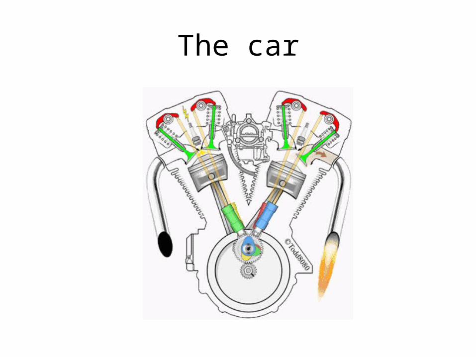
The car
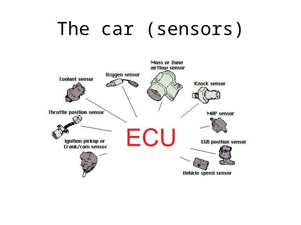
The car (sensors)
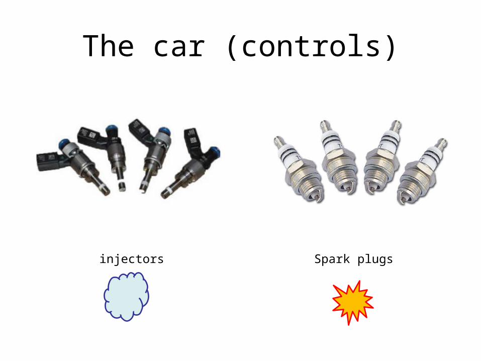
The car (controls)
injectors Spark plugs
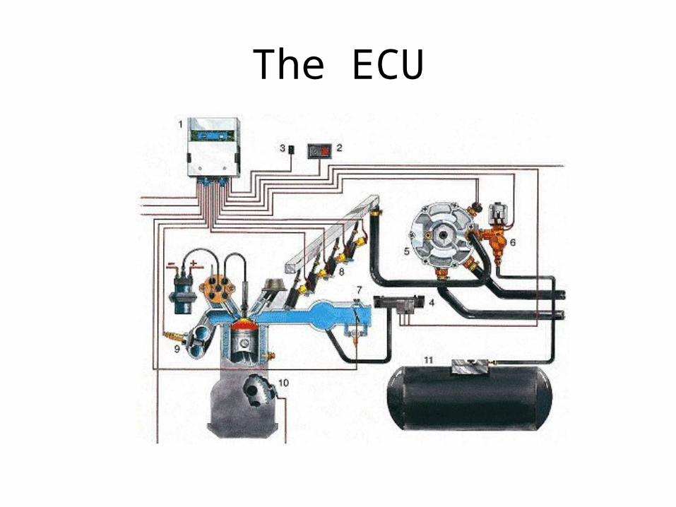
The ECU
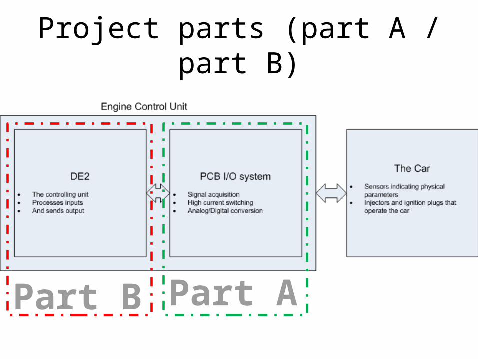
Project parts (part A / part B)
Part APart B
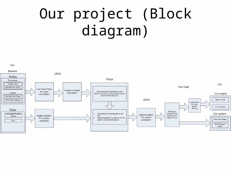
Our project (Block diagram)
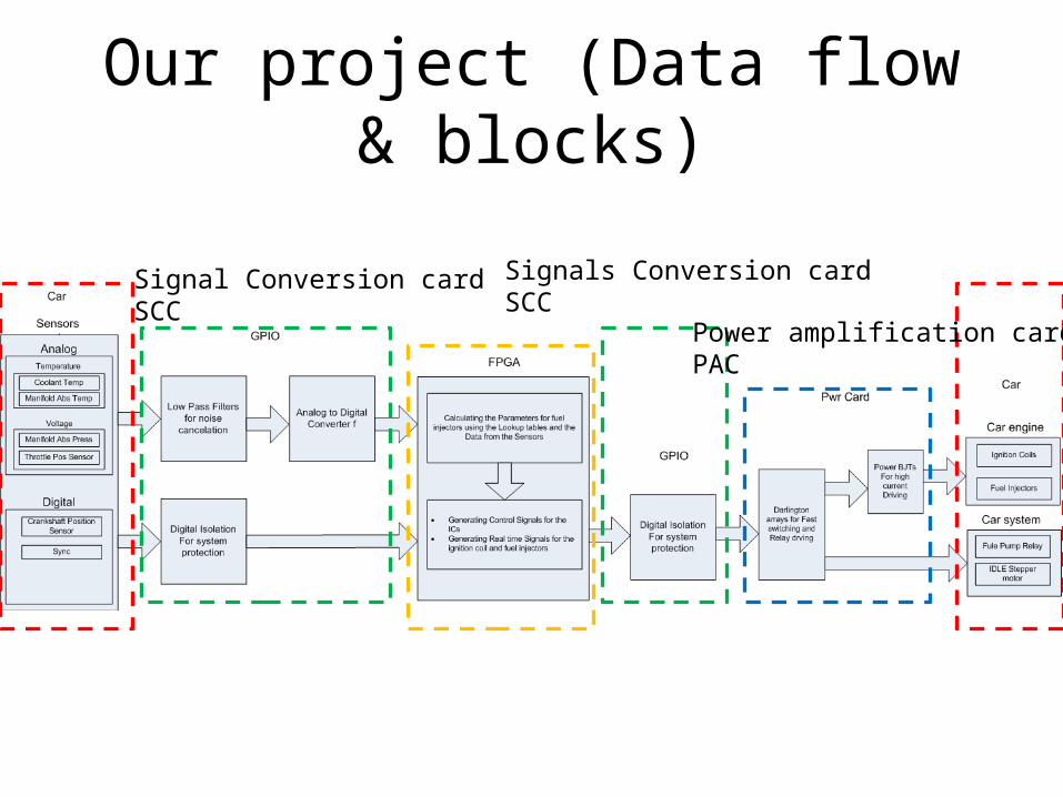
Our project (Data flow & blocks)
Signal Conversion cardSCC
Signals Conversion cardSCC
Power amplification cardPAC
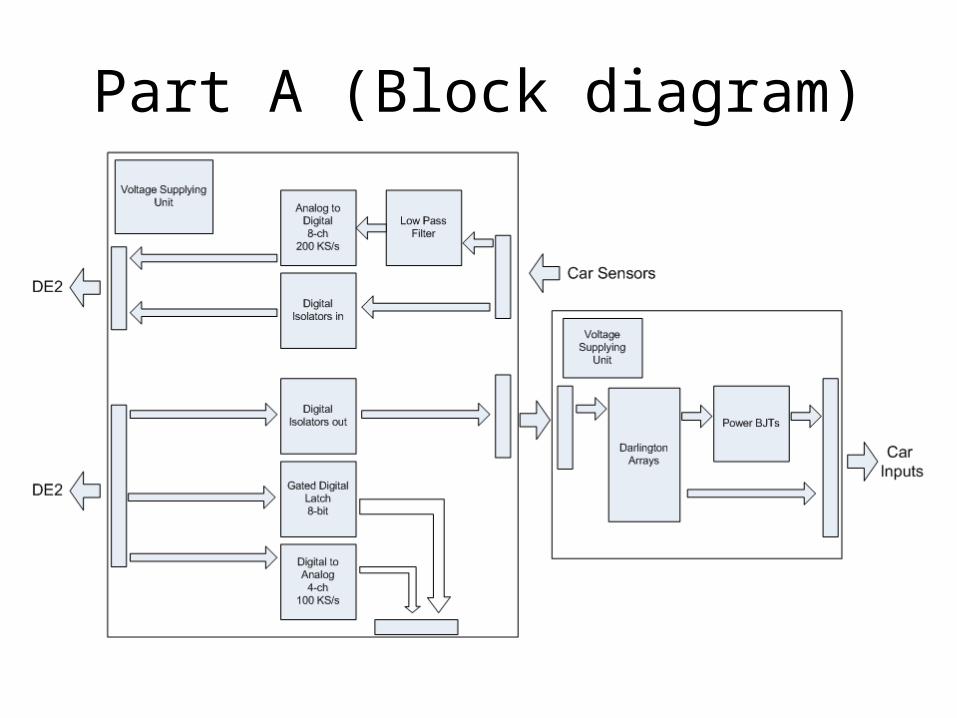
Part A (Block diagram)
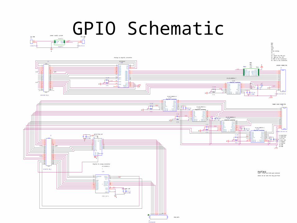
GPIO Schematic
U 1 4 AA D u M 1 4 0 0 B R W Z
?G N D 1 b2
V O D1 1V O C1 2V O B1 3
V I D6
V O A1 4
G N D 2 a9
V I C5 V I B4 V I A3
V E 21 0V D D 21 6
V D D 11
G N D 2 b1 5G N D 1 a
8 N C7
vcc5
vcc3
digital isolator
digital isolator
U 9 AA D 7 8 2 8 L N
D B 21 0 D B 1
9 D B 08
A 22 3A 12 4A 02 5
N C7
V D D2 6
V R E F (-)1 5V R E F (+ )1 6G N D
1 4 C S *1 8
A I N 82 7A I N 72 8A I N 61A I N 52A I N 43A I N 34A I N 25A I N 16
R D Y1 7
R D *1 2
I N T*1 3
D B 72 2 D B 62 1 D B 52 0 D B 41 9 D B 31 1
digital isolator
V D D
digital isolator
digital isolator
note : CC19 and CC20 were deleted
J 9
C O N N S O C K E T 1 6
123456789
1 01 11 21 31 41 51 6
C C 1 3
4 . 7 u
C C 1 4
1 0 0 n
put some vdd
0
C C 7
4 . 7 u
notes
C C 8
1 0 0 nU 1 6 A
A D u M 1 4 0 0 B R W Z
?G N D 1 b2
V O D1 1V O C1 2V O B1 3
V I D6
V O A1 4
G N D 2 a9
V I C5 V I B4 V I A3
V E 21 0V D D 21 6
V D D 11
G N D 2 b1 5G N D 1 a
8 N C7
0
MAPMATCPSSYNCTPS4free analogISI.S.S13: 5Vref for TPS out14: GND out for TPS15:VDD in for isolation16: Gnd in for isolation
V re f
0C C 2 14 . 7 u
C C 2 21 0 0 n
0
V re f
C C 34 . 7 u
C C 41 0 0 n
0
f ilt e rsf ilt e rs
M A P C L N M A P R A WM A T C L N M A T R A WTP S C L N TP S R A WC TS C L N C TS R A W
G N DV re f
J 1 0
C O N N P C B 2
12
0
J 1 1
C O N N P C B 2
12
0
C C 1 5
4 . 7 u
C C 1 6
1 0 0 n
C C 2 34 . 7 u
C C 2 41 0 0 n
V re f
U 1 3 AA D u M 1 4 0 0 B R W Z
?G N D 1 b2
V O D1 1V O C1 2V O B1 3
V I D6
V O A1 4
G N D 2 a9
V I C5 V I B4 V I A3
V E 21 0V D D 21 6
V D D 11
G N D 2 b1 5G N D 1 a
8 N C7
gnd
0
gnd
P w rS P L Y
P w rS P L Y
V D DG n d V re fB V ra w
0
V re f
0
C C 14 . 7 u
C C 21 0 0 n
0
vcc3
vcc5
V D D
0
C C 9
4 . 7 u
C C 1 0
1 0 0 n
R 7
3 k
J 1
H E A D E R 2 0 _ 2
24681 01 21 41 61 82 02 22 42 62 83 03 23 43 63 84 0
13579
1 11 31 51 71 92 12 32 52 72 93 13 33 53 73 9
R 85 k
POWER CARD CONNECTOR
6-INJECTORS4-IGNITION1-FP SIG1-IDLE AIR1-stepper1-starter15:VDD16:GND
C C 2 54 . 7 u
C C 2 61 0 0 n
V D D
J 2
H E A D E R 2 0 _ 2
24681 01 21 41 61 82 02 22 42 62 83 03 23 43 63 84 0
13579
1 11 31 51 71 92 12 32 52 72 93 13 33 53 73 9
V D D
U 1 5 AA D u M 1 4 0 0 B R W Z
?G N D 1 b2
V O D1 1V O C1 2V O B1 3
V I D6
V O A1 4
G N D 2 a9
V I C5 V I B4 V I A3
V E 21 0V D D 21 6
V D D 11
G N D 2 b1 5G N D 1 a
8 N C7
V re f
U 5
7 4 L S 2 7 3
VC
C2
0G
ND
10
D 13
D 24
D 37
D 48
D 51 3
D 61 4
D 71 7
D 81 8
C L K1 1
CL
R1
Q 12
Q 25
Q 36
Q 49
Q 51 2
Q 61 5
Q 71 6
Q 81 9
V D D
Analog to digital converter
gated dig out
U 2 A
S Y M 1 O F 1
?
?
A D 7 3 0 5 B R U Z
V O U TC2 0D B 2
1 2 D B 11 3
V O U TB1
D B 01 4
V O U TA2
V S S3
A 11 6 A 0 / S H D N1 7
W R *1 5V R E F4
V D D1 8
G N D5
L D A C *6
D B 77 D B 68 D B 59 D B 4
1 0 D B 31 1
V O U TD1 9
Digital to anaog converter
power supply system
C C 5
4 . 7 u
C C 6
1 0 0 n
0
V D D
12V RAW DE2 PWR
MAPMATTPSCTS
C C 1 1
4 . 7 u
C C 1 2
1 0 0 n
CPSISISSSYNC
SENSOR CONNECTOR
V D D
FRE OUTS
where do we take the dig gnd from
J 31 2 H E A D E R
1 2 3 4 5 6 7 8 9 10
11
12
C C 1 74 . 7 u
C C 1 81 0 0 n
J 8
C O N N S O C K E T 1 6
123456789
1 01 11 21 31 41 51 6
C C 2 74 . 7 u
C C 2 81 0 0 n
V D D
V D D
U 1 2 A
A D u M 1 4 0 0 B R W Z
? G N D 1 b2
V O D1 1 V O C1 2 V O B1 3
V I D6
V O A1 4
G N D 2 a9
V I C5V I B4V I A3
V E 21 0 V D D 21 6
V D D 11
G N D 2 b1 5 G N D 1 a
8N C7
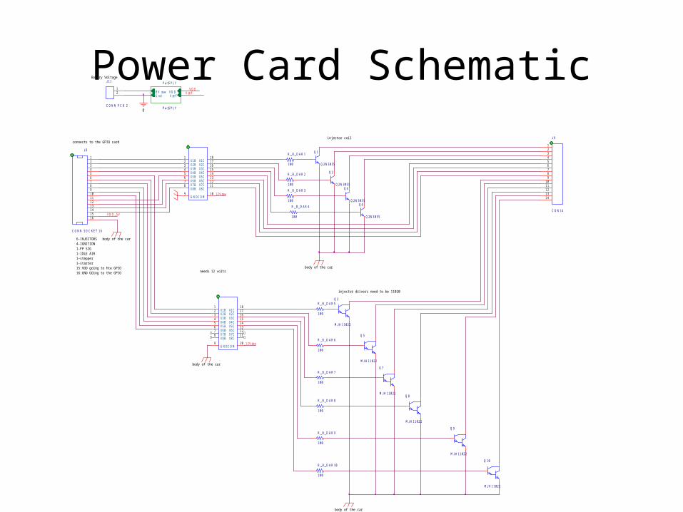
Power Card Schematic
J 9
C O N 1 4
123456789
1 01 11 21 31 4
X7 C1 2
X4 C1 5
X7 B7
X1 C1 8
X4 B4
X1 B1
G N D9
X6 C1 3
X3 C1 6
X6 B6
X3 B3
X8 C1 1
C O M1 0
X5 C1 4
X8 B8
X2 C1 7
X5 B5
X2 B2
X7 C1 2
X4 C1 5
X7 B7
X1 C1 8
X4 B4
X1 B1
G N D9
X6 C1 3
X3 C1 6
X6 B6
X3 B3
X8 C1 1
C O M1 0
X5 C1 4
X8 B8
X2 C1 7
X5 B5
X2 B2
needs 12 volts
Batery Voltage
R _ B _ D A R 2
1 0 0
R _ B _ D A R 3
1 0 0
Q 1
Q 2 N 3 0 5 5
Q 2
Q 2 N 3 0 5 5Q 4
Q 2 N 3 0 5 5
R _ B _ D A R 4
1 0 0
Q 6
Q 2 N 3 0 5 5
injector coil
Q 3
M J H 1 1 0 2 2
Q 5
M J H 1 1 0 2 2
R _ B _ D A R 5
1 0 0
Q 7
M J H 1 1 0 2 2Q 8
M J H 1 1 0 2 2
R _ B _ D A R 6
1 0 0
Q 9
M J H 1 1 0 2 2
Q 1 0
M J H 1 1 0 2 2
R _ B _ D A R 7
1 0 0
injector drivers need to be 11020
R _ B _ D A R 8
1 0 0
R _ B _ D A R 9
1 0 0
R _ B _ D A R 1 0
1 0 0
R _ B _ D A R 1
1 0 0
body of the car
body of the car
J 1 1
C O N N P C B 2
12
V D D _ 5 V
P wrS P L Y
P wrS P L Y
V D DB V ra wG n d V re f
0
V re fV D D
1 2 V ra w
6-INJECTORS4-IGNITION1-FP SIG1-IDLE AIR1-stepper1-starter15:VDD going to hte GPIO16:GND GOing to the GPIO
J 8
C O N N S O C K E T 1 6
1234567891 01 11 21 31 41 51 6
1 2 V ra w
body of the car
connects to the GPIO card
body of the car
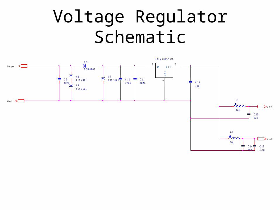
Voltage Regulator Schematic
V D D
B V ra w
V re f
G n d
C 91 0 0 n
C 1 02 2 0 u
C 1 11 0 0 n C 1 2
3 3 u
D 1
D 1 N 4 0 0 1
D 2D 1 N 4 0 0 1
D 3D 1 N 3 5 0 1
D 4D 1 N 3 5 0 1
U 1 L M 7 8 0 5 C / TO
I N1
O U T3
GN
D2
L 1
1 u H
L 2
1 u H
C 1 31 0 n
C 1 41 0 n
C 1 54 . 7 u
Testing plans
• Engine emulator (Lab-View)
What is left
• Printing the board• Designing the computing unit
DE-2• Integration• Testing
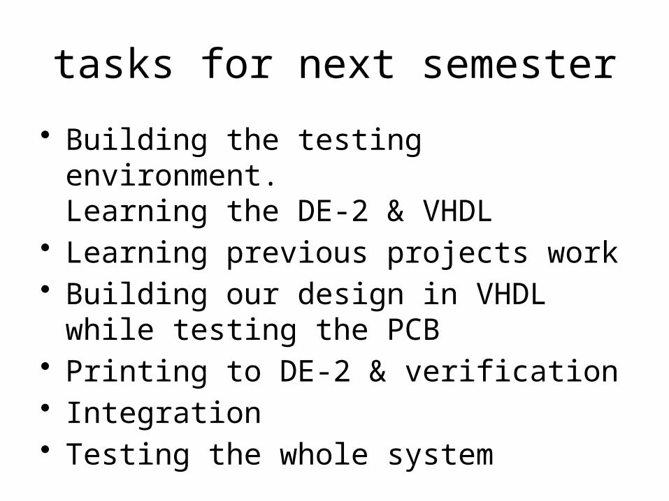
tasks for next semester
• Building the testing environment. Learning the DE-2 & VHDL
• Learning previous projects work• Building our design in VHDL
while testing the PCB• Printing to DE-2 & verification• Integration• Testing the whole system

Thank you