Embed Size (px)
Citation preview

R607 Philips Res. Repts 21, 477-495, 1966
THE SURFACE CHARGE IN OXIDIZED SILICON
by E. KOOI
AbstractInvestigations carried out to study the influence of oxidation and furtherheat treatments on the surface properties of silicon suggest that hydrogenand sodium impurities have a considerable influence. The presence ofsodium was checked by neutron-activation analysis, the influence of hy-drogen was investigated by heat treatments in a wet ambient. A model isproposed which explains qualitatively why the presence of sodium causesthe formation ofpositive surface charge during heat treatment and why atIow temperatures hydrogen (or water) can cause a decrease ofthis chargeas weIl as a decrease in the number of surface states. Further experimentsindicate that the sodium content ofSi02 films can be decreased consider-ably by heat treatments under conditions of Iow oxygen pressure.
1. Introduetion
The coating of silicon surfaces by thermally grown silicon-dioxide films hasalready been the subject of a large number of investigations, many of whichindicate that the resulting surface properties depend on various processingfactors. For example, a distribution of donors and/or acceptor impuritiesbetween the silicon and the oxide may occur during oxidation. These effectstend to make the surface more n-type or lessp-type than the bulk of the crystal.In practice, however, the surfaces are in many instances much more n-type thanmay be expected from these effects. This can be considered as being due to thepresence of positive charge in the oxide film and/or a predominanee of donor-type surface states to be related to centres in an interface region at theSi-Si02 boundary.The presence of surface states can be indicated by field-effectmeasurements, in
which one may make use of MOS (metal-oxide-semiconductor) structures. Bothdifferential MOS capacitance (C) versus d.c. voltage (V) and, inMOS transistors,drain-current (ID) versus voltage measurements are suitable methods. But inboth cases it is difficult to distinguish between interface states near the valenceand conduction bands and (fixed) charge in the oxide film, as they both causea displacement of the ID- V and C-V curves along the voltage axis. The slopeof the C-V curves may be affected by surface states distributed through theenergy gap. Whether such states are present or not, the voltage Vf at which theMOS capacitance corresponds to fiat-band conditions may be used as a referencepoint. From Vf a number (Nf) of surface charges per cmê at the Si-Si02 inter-face may be calculated (approximately: eNf = Cox Vf> e= unit charge,Cox = oxide capacitance per cm"). Values of Vf of the order of 1 V or lessmay be explained by a work-function difference between the metal electrode
478 E. KOOI
and the silicon. When charge is distributed through the oxide only an effectivepart of it is reflected in the value of N]. In general, however, the (positive)surface charge in oxidized silicon is located closely to the Si-Si02 interface asa large part of the oxide filmmay be etched away before N, is affected.
Changes in Nf may occur when ions are able to drift in the oxide film, forexample when a bias is applied across the MOS structure. Considerable insta-bility effects can be observed when the drift experiments are carried out atelevated temperatures (above about 100°C) and the metal of the MOS struc-ture is made the positive electrode. Snow et al. 1) have suggested that thesedrift effectsare due to the presence of alkali-metal impurities, especially sodium.Indeed it has appeared 2.3), and will be confirmed in this paper, that after ausual oxide preparation the top layer of an oxide film may contain a fairlylarge concentration of sodium ions. Snow et al. 4) report also that carefullyprepared oxide films do not show such instability effects and that the Nf valuesin MOS structures with oxide films of this type are low (in the range1-3.1011 cm-2, for oxidation at 1200 °C in oxygen). This suggests that excesssurface charge is due to (sodium) contamination. Indeed, it has been found thatthe n-type character of oxide-covered silicon surfaces can be increased by heattreatment in a sodium-containing environment 2.5).
In a publication of Revesz and Zaininger 6) a-relationship was shown to bepresent between the oxidation rate at the end of oxidation processes in oxygenand the resulting Nf values. The thicker the oxide film, the lower the oxidationrate and the lower the resulting N}, with a minimum of about 1012 cm-2•These authors relate these effects to disorder in the structure of the Si-Si02boundary, which will have more time to become ordered when the oxidationrate decreases. In accordance with this model the surface charge could be de-creased by heat treatment of oxidized samples in an inert gas. Further evidencefor the influence of the interface structure is given by the observations that thesurface orientation of the oxidized crystal can have a marked influence onNf 7.9) and on the number of surface states 10.11).
Effects of surface orientation and oxidation rate on the Nf values are con-firmed in the work presented here, but it proves to be possible to relate theseeffects to the presence of sodium at the Si-Si02 interface. However, apart fromalkali ions hydrogen is also known to be able to induce surface charge, althoughthe role of this element is more intricate. In earlier work 12.13) it was shownthat the number of surface states can be decreased by low-temperature treat-ments (below about 600°C) in the presence of hydrogen or water, whereassubsequently a slight decrease of Nf was often noted. At more elevated tem-peratures hydrogen treatments+") as well as treatment in water vapour 11)cause less decrease or even an increase of Nf. In this paper a model will beproposed which describes in a qualitative manner the relationship between N,and various experimental conditions.

THE SURFACE CHARGE IN OXIDIZED SILICON 479
2. Sample preparation and measurements
Silicon slices of both (111) and (lOO) surface orientation were cut from5 ohm-cmp-type (boron-doped) and n-type(phosphorus-doped) crystals, madeby the floating-zone method. After lapping with fine abrasive powder they wereetched in an aqueous solution of HF (50%) and KMn04 (4%) so that at leasta top layer of 50 microns was removéd. The samples were then washed in distilledwater and treated in hot nitric acid before oxidation.
Oxidation was carried out in a heated tube offused silica, either in dry (boilingliquid) oxygen or in wet oxygen (oxygen bubbled through purified water). Insome experiments the "dry" and "wet" oxygen were mixed to study the influenceof the water content of the oxidizing gas, which was checked at the end of thefurnace tube by dew-point measurements.
Oxides covered by a phosphate glass were prepared by subjecting oxidizedsamples to a P20s diffusion from a mixed Si02-P20s source for 30 minutesat 1050 oe in N2. The composition of the phosphate glass formed in this waywas about 7 Si02. P20s, its thickness approximately 0·1 micron.
For MOS-capacitancé measurements aluminium spots with a diameter of0·5 mm were deposited on the oxide film. The silicon substrate was not heatedduring the deposition; C- Vmeasurements were done with a measuring frequencyof 500 kc/so In the calculations to determine Vf, the work-function differencebetween aluminium and n-type silicon was assumed to be zero. The Nf valuesgiven in various tables are average values measured on one or more samples.The spread in results was always less than ± 10% of the indicated numbers.
The neutron-activation analysis of oxidized samples was carried out afterirradiating them together with a sodium standard for 3 hours in a neutron fluxof 1014 neutrons/cmê/s *). The reaction Na23 (n, y) Na24 results in activity ofNa24 (half life 15·4 hours). Sections of the samples were dissolved in suitablebuffered HF solutions, so that the sodium concentrations throughout the oxidefilms could be determined. For this purpose the solutions ofthe various sectionswere placed in a well-type scintillation detector coupled with a gamma spectrom-eter. Measurements were done on the l'38-MeV peak ofthe gamma spectrumof Na24. IJ,?-order to increase the efficiency of removing radioactive sodiumfrom the samples, all etch solutions used in the analysis were contaminated withnon-irradiated sodium chloride.
3. Experimental results
3.1. Surface charge in the presence of sodium contamination
3.1.1. Influence of oxide thickness
In table I a number of results have been summarized for p-type samples of
*) The irradiations were done in the reactor 2 at the Centre d'Etudes de l'Energie Nucléaireat Mol, Belgium.

TABLE I
Influence of oxidation time and further treatments on N, values (from the "flat-band" point ill 5OO-kcjsMOS C-V curves)of p-type Si with (111) and (lOO) surface orientation. For comparison numbers have also been given for (111) n-typesamples with an oxide thickness of 0·2 micron. Sodium concentrations are given for a top layer of 100A (total Na percm-) and in the remaining part of the films (average per cm")
oxida-after oxidation (02 1200CO) n, (cm-2 X 10-11) after various tr~atments
tion . oxide Na in Si02 Nf N2-H2O P20SP20S (1050 0c)
period thick- (cm"? X 10-11) 30 m 450 oe 30 m 1050 oe + N2-H2Oness top 100A rest (450°C)
(h) (urn) (cm=") (cm=") (111) (lOO) (111) (lOO) (111) (lOO) (111) (lOO)
t 0·1 28 11 10 7 15 3 10 31 0·2 5.1012_1013 2.1017_5.1017 15 (n : 11) 6 7 (n : 5) 3 7 (n : 2) 3 4·5 (n : 2) 34 . 0·4 11 5 3·5 1·5 2 4 1·5 2·5 .16 0·8 5.1012_1013 5.1016_1017 9 2·5 2·5 0·5 6 2 . 2 2,
.j:>.00o
t'1~sa

\
THE SURFACE CHARGE IN OXID1ZED SILICON 481
both (Ill) and (lOO) surface orientation, oxidized for various periods at1200 °C in oxygen (dew point -40 0C). The oxidation time isseen to have aconsiderable influence on Nf and the values for the (Ill) samples correspondclosely to those found by Revesz and Zaininger 6). The (IOO)-surface-oriented. samples, oxidized at the same time as the (111) samples show lower values ofNf> but in these samples, too, the lowest values are found for the thickest oxides.Comparison of n-type and p-type (Ill) samples shows lower Nf values for then-type material.
In a number of samples the sodium contamination was measured. It appearedthat a considerable amount of sodium was present on the top of the oxide(5.1013 to 1014 atoms per cm"), but the major part of it could be washed offm water. It is difficult to make out which part of this sodium contamination iscaused by the oxidation process. Samples from which the top layer (100 A) hadbeen removed before the irradiation showed afterwards the same sodium contam-ination on the outer oxide surface. In the results henceforth presented we will. therefore pay no attention to the sodium that could be washed off in water. Anexample of the sodium distribution in an oxidized sample is shown" in fig. 1 for
fm_maximumand
,_minimumi~ti~: oftheaveroge Naconc.ina section
4 Oxide I Silicon.
\Fig. 1. Distribution of sodium in an oxidized (111)-surface-oriented p-type silicon sample,found by neutron-activation analysis employing subsequent sectioning of the oxide film andthe silicon substrate.
an oxide thickness of 0·8 micron. Although the profile could not be determinedvery accurately, there is a distinct accumulation of sodium near the top of theoxide films and at the Si-Si02 boundary, in the latter case in the oxide as well asin the silicon. In comparing various samples, we found the amount of sodiumin the silicon to be much less reproducible than in the oxide film. Probably thesodium is not distributed homogeneously along the surface. It has been sug-gested 2) that the pile up of sodium in the oxide near the interface is responsiblefor the surface charge. Qualitatively such a relationship is certainly present. Intable I a number of average sodium concentrations in the top layer (100 A) and

482 E.KOOI
the remaining part of the oxide films have been given. The indicated numberscorrespond to results found for two to four samples with oxide thicknesses of0·2 and 0·8 micron. The sodium concentrations in the interior of the oxide filmare lowest for the thickest films. The spread in the results made it impossible todetect whether there was any difference in sodium-concentration profile in theoxides made on (111)- and (100)-surface-oriented samples. '
3.1.2. Influence of a PzOs diffusion
A gettering effect of the phosphate glass for sodium, reported earlier 2.3),was confirmed. However, the neutron-activation analysis showed that thegettering action did not remove all the sodium from the underlying SiOz.Probably there was some sodium profile in the SiOz film in these cases too, butthe sodium concentrations were too low to detect it accurately. Assuming thatthe amount of sodium at the Si-SfO; interface is indeed of large influence on thesurface charge, the presence of such a profile would cause the surface charge todepend on the distance between the Si-SiOz and the phosphate glass-Siö, inter-face. This was in fact found, as can be seen in table I: when samples with oxidefilms ofvarying thickness were subjected to the same PzOs diffusion the largestamounts of charge were found for the thinnest films.
3.1.3. Influence of water vapour during heat treatment
It is apparent from table I that the surface charge can also be lowered whenthe oxidized samples are treated in wet nitrogen at 450 oe. This effect is stillpresent (although less) for samples covered with a phosphate glass. A possibleexplanation will be given later (sec. 4).
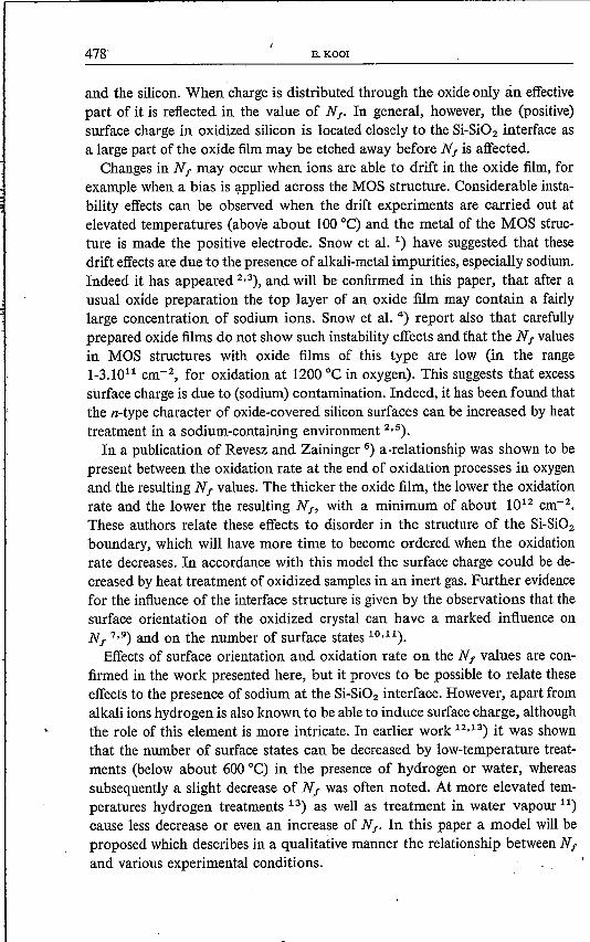
The gas used for preparing the samples mentioned in the previous section wasnot extremely dry. To investigate the influence of water in the oxidation gas wemade oxide films of approximately 0·2 micron thickness by oxidation in oxygenwith varying water content, using further the same oxidation system as used forthe samples oftable I.Together with (in two cases) the average sodium concen-tration in the oxide film, the results are shown in table 11. The surface chargeis largest for the cases that the gas was very dry, but for the higher watercontents, too, an increase is observed. A tendency for the amount of sodiumto decrease when the water content was increased can be noted.
3.2. Oxidation under conditions of little sodium contamination
The results of table I show that the surface concentration of sodium in theoxide film is the same for oxidation during I hour and 16 hours. This indicatesthat in these cases the gaseous environment during oxidation contains a fairlyconstant amount of sodium impurities. Alkali ions which, are adsorbed duringetching or further "cleaning" treatments would probably tend to disappearduring heating if the gaseous ambient were free of sodium. It is feIt that the
THE SURFACE CHARGE IN ·OXlDIZED SILICON 483
TABLE Il
Nf values, determined from C-V curves measured at 500 kc/s, before and aftera treatment in wet N2 at 450 oe (30 min), for (111) 5 ncm p-type siliconsamples oxidized at 1200 oe in oxygen of different humidity. The oxide thick-ness is in each case approximately 0·2 micron. Sodium conoentrations weremeasured on two series of samples made under different conditions
dew point oxida-Na in Si02 Nf (cm-2x 10-11)
of O, tiontop 100 A rest after oxidationCOC) (min) (cm-2) (cm-3) oxidation + wet N,
-70 60 21 7-40 60 5.1012_1013 2.1017-5.1017 15 7-34 60· 14 7-20 60 / 11 5-6 60 10 625 30 2.1012 4.1016 7 665 12 9 690 7 15 8
main source of sodium is due to contamination of the vitreous silica tube inwhich the oxidation was carried out. Particularly contamination of its outersurface (e.g. dust) may have been the predominant source because the alkaliions move easily through Si02 at elevated temperatures. However, the oxidizinggas (e.g. not sufficiently purified water) and drying agents for it can also be asource of contamination.
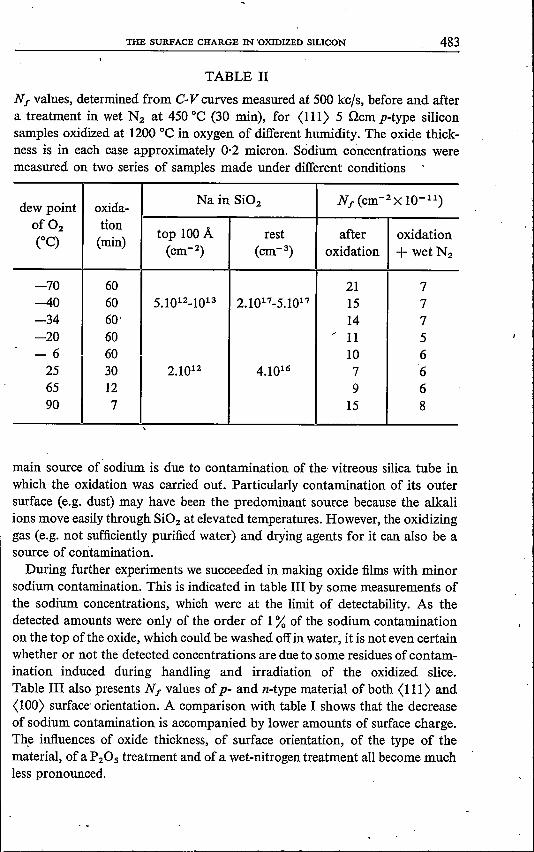
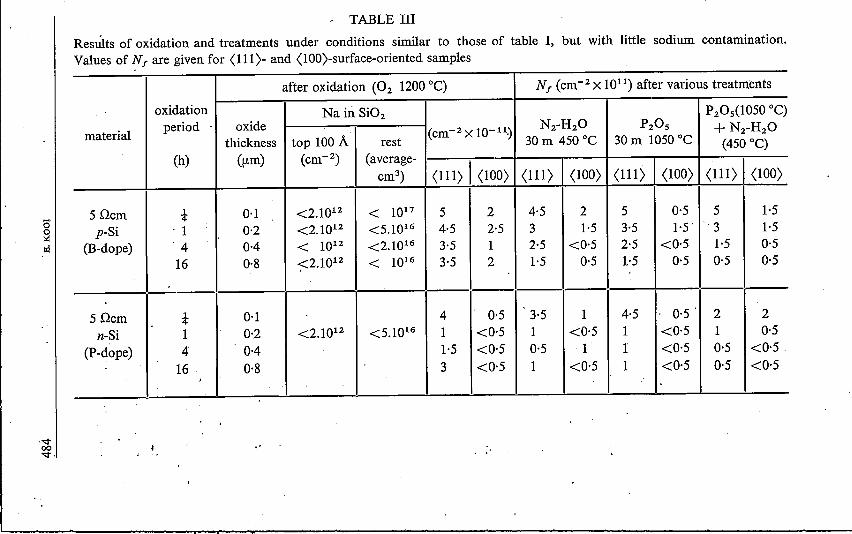
During further experiments we succeeded in making oxide films with minorsodium contamination. This is indicated in table III by some measurements ofthe sodium concentrations, which were at the limit of detectability. As thedetected amounts were only of the order of 1% of the sodium contaminationon the top of the oxide, which could be washed off in water, it is not even certainwhether or not the detected concentrations are due to some residues of contam-ination induced during handling and irradiation of the oxidized slice.Table III also presents Nf values of p- and n-type material of both <111) and<lOO) surface orientation. A comparison with table I shows that the decreaseof sodium contamination is accompanied by lower amounts of surface charge.The influences of oxide thickness, of surface orientation, of the type of thematerial, of a P20S treatment and of a wet-nitrogen treatment all become muchless pronounced.
saIII
TABLE IIIResults of oxidation and treatments under conditions similar to those of table I, but with little sodium contamination.Values of Nf are given for (111)- and (IOO)-surface-oriented samples
after oxidation (02 1200°C) Nf (cm=ê x 1011)after various treatments
oxidation Na in Si02 P20s(1050 0c)
materialperiod . oxide (cm-2 X 1O-11~ N2-H2O P20s + N2-H2O
thickness top 100A rest 30 m 450 oe 30 m 1050 oe (450°C)(h) (um) (cm=") (average-
(111) I (lOO) (111) I (lOO)cm") (111) (lOO) (Ill) (lOO)
5Qcm t 0·1 <2.1012 < 1017 5 2 4·5 2 5 0·5 5 1·5p-Si ' 1 0·2 <2.1012 <5.1016 4·5 2·5 3 1·5 3·5 1·5. 3 1·5
(B-dope) '4 0·4 < 1012 <2.1016 3·5 1 2·5 <0·5 2·5 <0·5 1·5 0·516 0·8 ~2.1012 < 1016 3·5 2 1·5 0·5 1·5 0·5 0'5 0·5
5Qcm t 0·1 4 0·5 3·5 1 4·5 . 0·5' 2 2n-Si 1 0·2 <2.1012 <5.1016 1 <0·5 1 <0·5 1 <0·5 1 0·5
(P-dope) 4 0·4 1·5 <0·5 0·5 1 I <0·5 0·5 <0·516 ' 0·8 3 <0·5 1 <0·5 1 <0·5 0·5 <0·5.
''<t00'<t. "

THE SURFACE CHARGE IN OXIDIZED SILICON
3.3. Summary of results
In a next section an attempt will be made to explain the various experimentalresults in terms of a physical-chemical model of an oxidized silicon surface. Weshall now review the observed phenomena, including some results of earlierwork 12.13).
(1) In conventional silicon-oxidizing techniques contamination of the Si-Si02system by sodium may occur during oxidation.
(2) The sodium concentration is then highest at the top of the oxide film, butthere is also accumulation in the oxide and the silicon near the interface. ,
(3) The concentration of sodium at the Si-Si02 boundary becomes lower whenthe oxidation rate decreases, i.e. when the oxide has grown thicker.
(4) In the presence of sodium contamination the surface charge (Nf) decreaseswhen the oxidation rate decreases.
(5) The value of Nf depends on the surface orientation of the silicon crystal,but most markedly when sodium is present.
(6) The value of Nf tends to be lower for n-type than for p-type material,especially in the case of <111> surface orientation and of sodium beingpresent.
(7) A P20s diffusion (especially when carried out in a non-oxidizing gas) tendsto reduce the amount of surface charge. The phosphate glass tends to gettersodium.
(8) The-action of water vapour on the surface charge depends strongly on thetemperature of heating. Below about 600 oe a considerable decrease' in.N, values may be noted. At more elevated temperatures, however, suchtreatments might cause an increase 11.14). Hydrogen acts in a similar wayas water vapour, but the residual surface charge tends to be larger, especiallyat temperatures above 500 oe 13). The hydrogen may also be evolved by areaction between aluminium on the oxide and surface hydroxyl 12).
(9) After oxidation or heat treatment in a dry environment, large numbers ofinterface states can be present 10-16). These may be distinguished asacceptor-type states close to the conduction band and donor states nearthe valence band 11). They are probably due to the presence ofunsaturatedsilicon bonds at the Si-Si02 interface.
(10)The number of surface states can be reduced drastically by low-temperatureheat treatments in the presence of hydrogen or water 12.13), i.e. the sametreatment which can cause a decrease in Nf (note (8)).
4. Discussion
4.1. Intelface states and the ''flat-band'' surface charge
Before we shall discuss a model of an oxidized silicon surface, we will consider
485

486 E.KOOI
what kind of information is really obtained from the measurement of the "fiat-band" point in a MOS C-V curve. Note (10) of the previous section suggests thatthe value of Nf is closely related to the surface states indicated in note (9). Themajor part of these interface states can be localized in regions from 0·1to O·3 eVfrom the silicon valence and conduction band 10.11): In fiat-band conditions onp-type material some states may be positively charged, and on n-type material thecharge in the interface states may tend to be negative. That such situations canindeed occur was shown by Whelan 15) from C-Vmeasurements at frequenciesbetween 20 and 100Mc/s. However, at a frequency of 500 kc/s as used in thepresent work, the interface states can still follow the a.c. signal !"). When thisoccurs, the measured MOS capacitance is not in accordance with the bandbending at the given d.c. voltage. Instead the oxide capacitance may be meas-ured, as the states are situated at the oxide-silicon interface. This may occur overa wide range of the applied d.c. voltage. In the middle of the energy gap thereare generally not a sufficiently large number of surface states to cause the ex-change during the a.c. signal to occur completely at the interface. Consequently,also' in the presence of a large number of surface states near the valence andconduction band's, the capacitance decreases below the oxide capacitance whenthe d.c. voltagé causes the surface to be nearly intrinsic. The slope of the C-Vcurve looks then fairly ideal, i.e. as if there were no surface states present 15).There may be a displacement along the voltage axis, from which a number ofcharges Nf can be calculated. These Nf values may thus not always correspondto real fiat-band conditions, but instead to a situation in which the charge in theacceptor-type interface states near the valence band and the donor-type interfacestates near the conduction band is approximately zero. This consideration leadsto the conclusion that the N f values determined from a 500-kc/s C-V curve do notgive an indication ofthe number of these surface states. Instead, N, should berelated to a number of other states which contain a more or less fixed (positive)charge. One is inclined to ascribe these fixed charges to centres in the oxidestructure. However, as was stated before, it is not possible from the present ex-perimental information to distinguish between oxide states and donor-typeinterface states close to or above the conduction-band edge of the silicon..More evidence that the surface charge corresponding to Vf is present in other
states than those indicated in .note (9) of the previous section, is obtained fromthe observation 11.13) that a P20s diffusion causes in general an increase ofthe number of surface states but a decrease of the "fiat-band" voltage deter-mined from 500-kc/s C-V curves.In a model for an oxidized silicon surface the centres which carry the surface
charge Nf should thus be different from those causing the interface states nearvalence and conduction band. On the other hand a chemical relationship shouldbe present (sec. 3.3, note (10)). The considerations given above indicate also thatthe differences noted between Nf values on n-type and on p-type samples

THE SURFACE CHARGE IN OXIDIZED SILICON 487
(sec. 3.3, note (6» cannot completely be explained by a difference in the occupa-tion of the indicated interface states. There is probably also a difference in thenumber of other donor-type states, especially when impurities like sodium arepresent.
4.2. Unsaturated silicon bonds at the Si-Si02 interface
The valence of four which silicons shows can be related to the fact that asilicon atom has four electrons in its outer shell. When such an atom is bondedto less than four other atoms, the remaining unpaired electrons may be consider-ed as unsaturated. They may bè present as "dangling" bonds or give rise todouble bonds between two atoms. In the following model wewill try to considerunsaturated silicon bonds as a reason for various surface phenomena. Forsimplicity we will consider them as dangling bonds, of which wemay distinguishvarious types, depending on their location in the Si~Si02 structure.À dangling bond in the silicon lattice, i.e. an unpaired electron at a silicon
atom bonded to three other silicon atoms, further indicated as Si(3), may beconsidered as being able to act as an acceptor
Si : Si : Si+ e: ~ Si : Si : Si.. ..Si Si
or (1)
However, the Si(3) centre mayalso be able to give. off the unpaired electronand act as a donor:
(2)
These types of centres may be assumed to occur at a clean silicon surface, butalso when it is covered by Si02. Because of some misfit or lack of oxygen, not allsilicon bonds may be saturated. The Si(3)centres may thus be considered as thereason for the (acceptor-type) surface states near the conduction band and the(donor) states near the valence band. During heat treatment ~n the presenceof hydrogen the acceptor and donor action may disappear due to the reaction
(3)
SiH bonds are probably less stable at elevated temperature and this explains whyespeciallylow-temperature heat treatments in the presence of H2 or H20 areable to cause the disappearance of interface states.Apart from Si(3) centres, the Si-Si02 interface may also contain unsaturated
silicon bonds at silicon atoms, which are bonded already to one, two or threeoxygen atoms, and to two, one or zero silicon atoms, respectively. These maybe indicated as Si(2), Si(l) and Si(O)centres. The Si(O)centre may also be con-

488 E. KOOI
sidered as a half oxygen vacancy or as an Sp+ ion when the oxide structure isconsidered to be ionic. Summarizing:Si(O): 0 : Si: 0 or 02- sp+ 02-
o 02-
Si(1): o :Si:OSi
.Si(2): Si: Si: 0Si
SP) : Si : Si : SiSi
Due to the electronegative character of the surrounding oxygen ions theSi(O)centre can be supposed to act more readily as.a donor than as an acceptor:
or
Si(O)+t Si(o)++ e:
02-SP+02- +t 02- Si4+ 02- + e-.02- 02-
(4)
(5)
Also the Si(2) and Si(l) centres probably have more tendency to a donoraction than to an acceptor action, compared to the Si(3) centre.The surface charge measured from the flat-band point in a (500-kcjs) c-v
curve must be related to centres with donor action, a role which might thus befaulfilled by the Si(O),Si(l) and Si(2) centres. The Si(O)centres may be presentas well in the oxide as at the Si-Si02 interface, whereas one is inclined to con-sider the Si(1)and Si(2)centres to occur only at the interface. The donor actionof the centres is in all cases related to the fact that they represent an incompleteoxidation product of silicon. We will further consider the Si(O)centres as anexample, but one should thus realize that the Si(1)and Si(2)centres may behavesimilarly. A possible relationship between the 'presence of Si(o)+ centres andimpurities will be discussed in the next sections.Until so far we have considered the Si(3)centres to cause both the presence
of the acceptor- and the donor-type interface states near the conduction andvalence band, respectively. It is not impossible, however, that at least a partof the donor states is due to Si(2) or Si(1) centres. All centres may react withhydrogen at low temperature, although some difference in reaction velocity orreaction equilibrium might be expected. This might explain why in certainhydrogen treatments the donor states near the valence band disappear lesseasily than the acceptor states near the conduction band 16).
4.3. The role of hydrogen in the structure of silicon dioxide
The structure of Si02 may be considered as a network in which Si4+ ions are

THE SURFACE CHARGE IN OXIDIZED SILICON
connected via bridging 02- ions. Non-bridging 02- ions may also be presentwhen they are accompanied by "network-modifier" cations, such as protonsand alkali ions. Such combinations can be assumed to be present due to incor-poration of H;O and Na20 and so on in the Si02• The combination of a non-bridging oxygen ion and a proton is often called a hydroxyl group. It is wellknown, however, that hydroxyl groups can also form in Si02 as a -result ofheating in hydrogen 17.18). This reaction has been described as
Si4+ 02- Si4++ t H2 +t Si4+ 02- H+ + SP+,. although also the following possibility was considered 18):
Si4+ 02- Si4+ + H2 +t Si4+ 02- H+ + H-SP+.In the previous section the Sp+ ion (Si(Olcentre) was assumed to be able to
act as a donor at the silicon surface (reactions (5) or (4)).A reaction like (6)may thus be the reason for the formation of surface charge during heat treat-ment in hydrogen at elevated temperature (at too high temperatures - aboveabout 1000 °C - the reducing action of H2 may even cause the formation ofvolatile SiO). It was suggested before that the SiH bonds become less stable atelevated temperature, but reaction (7) cannot be excluded and may limit thenumber of surface donors. At low temperatures the formation of SP+-H (orSi(Ol-H)seems even very probable (reaction (3)).
4.4. Oxidation of silicon in water vapour
Oxidation of silicon in water vapour can be assumed to result also in the forma-tion of hydrogen at the Si-Si02 interface and one may therefore expect reac-. tion (6) to occur or, better, the oxidation is not likely to be completed directlyat the interface due to a certain virtual hydrogen pressure at that place: Indeedit has been found that the efficiency of oxidation in steam can be much less than100 per cent 19), while infrared measurements have been reported 20) which in-dicate a decreasing concentration of Si-O bonds in the oxide from the top to-wards the silicon surface. The concentration of hydrogen in steam-grown oxidefilms has been shown to be in the order of 1020 cm-3,28). In the top layerof the oxide the hydrogen may be present due to the incorporation of wateror OH groups. In the region near the interface the water tends to be reducedand OH groups combined with Sp+ ions or SiH groups may be.present. Dueto the donor action ofthe Sp+ ion (Si(Olcentre) a positive oxidecharge may tendto be formed, with the compensating electron occurring in the silicon:
Si4+ 02- H+ sp+ +t Si4+ 02- H+ Si4+ + e: (Si) (8)or Si - 0 - H Si(Ol+t Si - 0 - H Si(o)++ e: (Si). (9)
The presence of these positive centres may also be described as an incompleteoxidation of silicon, which would be completed by reduction of the proton:
Si4+ 02- H+ Si4++ e: (Si) +t Si4+ 02- Si4+ + t H2. (10)
489
(6)
(7)
490 E. KOOI
Oxidation of silicon in steam may thus result in the formation of positive oxidecharge due to the formation ofhydrogen at the Si-Si02 interface and its reducingaction on Si02• The charge mayalso, however - although this means essentiallythe same - be related to incomplete oxidation of silicon or incomplete reductionofthe water species. Whether one wants to ascribe the positive surface charge tothe non-reduced protons or to the donor action ofthe Si(O)centres (compare thereaction products of reactions (8) and (9)), does not make any essentialdifference.The reduction of the positive surface charge by treatment in hydrogen at arelatively low temperature may be ascribed to the formation of Si(O)-Hbonds.The donor action of the Si(O)centres is then lost. One mayalso say that thepositive charge ofthe non-reduced protons tends now to be compensated by thenegative charge in the Si(O)H(Si4+H-) bonds instead of by electrons in thesilicon. In the case of low-temperature treatment in the presence of water notonly the formation of Si(O)-Hbonds but also the formation of Si(O)-OHcom-binations may play some role in the reduction of surface charge.
4.7. Oxidation of silicon in wet oxygenIn this case there are two oxidizing species, oxygen and water. Hydrogen
formed by the reduction of water at the Si-Si02 interface may move back to-wards the Si02-gas interface, until it meets neutral oxygen (somewhere in theoxide or at the oxide-gas interface) with which it reacts, after which oxygen ionstogether with protons move back to the silicon, and so on. In this way traces ofwater may act as a catalyst during oxidation in dry oxygen. Indeed it has beenfound that silicon oxidizes very slowly in extremely dry oxygen 21). The virtualhydrogen pressure at the Si-Si02 interface will become lower when the oxygencontent of the gas is increased, and this may explain why steam-grown oxidestend to induce more positive surface charge than (alkali-free) films grown in"dry" oxygen. Itmay be remarked that the values of Nf given in table II foroxidation in wet oxygen cannot be ascribed completely to the role of hydrogen,as these films were not sodium-free.
4.6. The role of sodium in the Si-Si02 system
We have seen that during oxidation in "dry" oxygen the presence ofhydrogen(water) may help the transport of oxygen ions through the oxide film. Apartfrom that, the presence of protons may catalyse the interface reaction due tothe formation of intermediate structures such as shown in eqs (8) or (9). Asimilar role may be ascribed to sodium, which may be assumed to be presentas sodium oxide in the oxidizing gas. Sodium ions moving together with oxygenions towards the Si-Si02 interface tend to be reduced there. "Neutral" sodiumtends to diffuse into the silicon and back in the direction of the oxide-gas inter-face. This may be considered as the reason for the peak in the sodium coneen-tration at the Si-Si02 interface shown in fig. 1. Although neutral sodium in

THE SURFACE CHARGE IN OxrDIZED SILICON 491
"Si02 probably does not exist, the virtual sodium pressure may give rise totheformation of associates of Na+ and Sp+ ions: Si4+ 02- Na+ sp+ or, incovalent notation, Si-O-Na Si(O). The motion of neutral sodium in Si02 maybe considered as displacements of these centres due to motion of Na" ionstogether with unpaired electrons at the Si(O) centres. These electrons mayalsobe given off to 'the silicon, so that donor action occurs. The ionized donorsSi4+ 02- Na+ Si4+ or Si-O-Na Si(o)+ may also be considered as intermediatereaction products. The density of these centres depends on the virtual sodiumpressure at the interface. This pressure is determined mainly by the transport'of Na" ions towards the Si-Si02 interface and the motion of "neutral" sodiuminto the silicon or back towards the oxide-gàs interface, and thus by the oxida-tion rate and the sodium contamination in the oxidizing gas. This explains whythe concentratien of sodium at the Si-Si02 interface and the oxide charge tendsto decrease with increasing oxide thicknesses. Table I shows that the effect ofoxide thickness remains present after a P20S diffusion. This is probably due tothe fact that some oxidation of silicon still occurs during the diffusion (P20Smay act as a source of oxygen). This wou1d then mean that there is also sometransport of Na+ ions towards the Si-Si02 interface. In other experiments wehave observed that the Nf values become higher when the P20S diffusion iscarried out in oxygen instead of in an inert gas.
Not only does the virtual pressure of sodium at the Si-Si02 interface deter-mine the surface charge. There is also an apparent influence of the interface
, structure, as is indicated by the different values of Nf found after oxidation ofsamples with different surface orientation. It is 'remarkable that the differencesare most pronounced when sodium is present (compare tables I and 1II). Con-sidering the formation of positive surface charge again as a result of a reducingaction of sodium on the Si02 structure, it is plausible to assume that this occursmost readily in the interface region with the largest misfit between the structuresof the silicon and the oxide. From these points of view the results suggest thatthe misfit is larger for (111) than for (lOO) surfaces. This is also consistent withthe observation that the number of interface, states, which in this work areattributed to Si(3) centres, is largest for (111) surfaces 10.11).
As was stated earlier 14), the explanation for the effect of surface orien-tation mayalso be described as follows. Structures like Si-O-Na Si(o)+(Si4+ 02- Na+ Si4+) represent an incomplete oxidation product of silicon.Transformation of these structures to Si-O-Si means a decrease of positive(oxide) charge (comparable to reaction (10)):,
Si-O-Na Si(o)+ + e-(Si) +t Si-O-Si + Na. (11)
For this transformation the two silicon sites should be at a suitable distance,and the number of Si(o)+ centres associated with the presence ofsodium maythus be affected by the misfit between the oxide and the silicon structure. The
492 a xoor
experience that oxidizing treatments in the temperature range 600-1000 oecause more surface charge than oxidation at higher temperatures 6.11) may beexplained by a high activation of such a transformation. This explanation comesvery close to that of Revesz and Zaininger, 6): in oxidation processes at lowertemperatures the interface structure has more difficulty in becoming ordered.
In the presence of sodium there is also a clear influence of the type of material.The lower values of Nf for n-type instead of p-type material were also found byRevesz and Zaininger 6), who suggested that the difference might be explainedby incorporation of phosphorus in the interface structure. Considering thepositive charge as being present in the oxide, it is more likely that the iargersurface charge in p-type samples is due to incorporation of boron in the oxidestructure, resulting in some way in an increased number of donor-type centreswhen sodium is also present. The difference between n- and p-type samplesmight also be explained by a difference in the frozen-in distribution of electronsbetween oxide and silicon due to a difference in electron concentration at thesilicon surface during cooling. To eliminate this effect we did experiments inwhich the samples were exposed to light during heat treatment and cooling.Although some influence was noted, the major part of the difference of Nf inn-type and p-type samples remained.It appears from table IJ that alkali impurities are more effective in creating
positive surface charge then hydrogen. This may be due partly to the possibilityof formation of covalent bonds between Si(O)centres and hydrogen. Formationof Si(O)-R bonds and perhaps some Si(O)-OR bonds can also explain that thecharge due to sodium can be decreased by heat treatment in water vapour andhydrogen. This can be understood to occur most effectively at low temperaturesbecause of the instability of SiR bonds at elevated temperatures. Some exchangeof sodium ions by protons may also occur and in this way the sodium coneen-trations may be lowered (particularly during heating at high temperatures,table 11).
During various treatments there mayalso occur redistributions of charge inthe oxide, which can cause changes in the C- V curves. These effects and alsothe influence ofthe way of cooling have been neglected in the given model. Thereare certainly still other effects and impurities than those mentioned which canaffect the surface properties of oxidized silicon. As an example we may remindof the fact that. even temperature gradients during heat treatment can affect thecharge distribution in an oxidized system 22). It is felt, however, that the givenmodel gives a useful qualitative explanation of many phenomena which havebeen observed in the Si-Si02 system.
4.7. Instability effects due to sodium-ion drift
In oxide-coated silicon devices ion-drift effects may cause instability. This isin particular the case in devices containing MOS structures, where high electric

THE SURFACE CHARGE IN OXIDIZED SILICON 493
fields may be applied across the oxide film. It has been shown 15) that the sur-face charge in oxide films prepared in a wet ambient can be fairly stable duringheat treatments with a negative bias on the metal electrode of a MOS structure.This indicates that the protons present in the oxide film are not displaced easily.Under the same conditions somewhat larger changes of the oxide charge werefound when the oxide was prepared in dry oxygen. This is probably due todisplacement of Na+ ions. However, it has not proved possible to make thesurface charge zero or negative with such a treatment, except when the oxidecontains trivalent ions (for example BH or AP+) 23.24). From literature aboutvitreous systems it is known that the motion of univalent ions is then mucheasier 25). In general, however, MOS structures show little instability duringbias-heat treatment with a negative bias on the metal electrode, which indicatesthat the sodium ions in the oxide films are not displaced very readily either.
Serious instability effectsmay be noted when the metal electrode is made posi-tive during heat treatment. This is probably related to the drift of sodium ions,a considerable number of which may be present at the top of the oxide films.The drift effects are enhanced when some moisture is present 26), suggestingthat instabilities due to proton drift may occur too. However, it seems alsopossible that water decreases the activation energynecessary to make the sodiumions free to move into the oxide film. Instability effects can be limited by ex-cluding contamination from alkali ions during the processing or by getteringthem with the help of a phosphate glass. In the next section we will discuss analternative method of removing alkali ions from oxide films.
5. Reducing treatments of oxidized silicon
Apart from at the Si-Si02 interface, the hydrogen and sodium concentrationin the oxide may be related to an excess of oxygen being present. Kats 27) hasshown that quartz can be freed from hydroxyl (according to infrared measure-ments) by heat treatment in an inert gas, or more effectively in a reducingenvironment of carbon monoxide. The same effect can be expected to occur inthe case of sodium, so that such a treatment might offer the possibility of lower-ing the sodium concentrations in oxide films on silicon. Heat treatments in thepresence of carbon monoxide or in high vacuum has the disadvantage that theoxide film tends to disappear due to the formation ofvolatile SiO.We have done'experiments under reducing conditions in which this evaporation was avoidedby heating the oxidized slices in an evacuated quartz capsule together withsilicon powder. During heating a gas mixture forms, consisting mainly of SiO,formed by reaction between the silicon powder and the quartz wall, and furthera very low concentration of silicon and oxygen. In such an environment theoxygen content of the oxide tends to become homogeneous throughout the film(at both sides excess oxygen is extracted by the silicon) and under these con-ditions Na20 and H20 tend to be reduced to Na and H2' respectively. The
494 E.KOOI
sodium is then redistributed between the various phases present. Oxide filmsof 0·2 micron thickness made by oxidation of (l11)-surface-oriented p-typesilicon at 1200 oe in oxygen, showed a decrease in Nf from 15.1011 before to1-3.1011 cm-2 after a treatment under such reducing conditions at 1050 oe for30 minutes. Neutron-activation analysis showed a decrease of the averagesodium concentratien in the oxide by about a factor of ten, whereas diffusioninto the silicon proved to have much increased. The low values of Nf would
, not be expected to occur if the sodium pressure in the system were high. Thesame may be said for the hydrogen pressure. We have indeed observed that Nfdid not become very low when the system was not made sufficiently clean anddry. A disadvantage of the method is that the oxides may become leaky atweak spots. _
The experiments done under these reducing conditions indicate that oxygenvacancies which might be expected to form in the oxide, do not induce muchpositive surface charge. During bias tests carried out at 150 oe, MOS structuresmade of oxide films with low sodium content showed no or little instabilityphenomena either, and therefore it is apparent that alkali ions rather than theoxygen vacancies are the main reason for ion-drift phenomena in oxidizedsilicon.
6. Conclusions
Positive surface charge in oxidized silicon can be caused by to the presence of avirtual sodium and hydrogen pressure at the Si-Si02 interface during heat treat-ment. These pressures are related to the amount of sodium and hydrogen (water)in the oxidizing gas and the oxidation rate of the silicon. At low temperatureshydrogen and water tend to reduce the interface charge. These effects show a /similarity to the disappearance of surface states during such treatments. Bothlow-temperature effects can be explained by the formation of SiH bounds.
The sodium concentration in thermally grown oxide films can be diminishedby heat treatment under conditions of low oxygen pressure. Such treatmentscan be used to decrease the fiat-band surface charge and to increase the stabilityof MOS structures.
Acknowledgement
The author is indebted to J. Schatorjé and W. Verkuilen for sample prepara-tion and measurements, to M. L.Verheijke and J. P. M. Damen for the neutron-activation analysis and to L. J. Tummers, M. V. Whelan and F. C. Eversteijnfor stimulating discussions and critical reviews of the manuscript ..
Eindhoven, August 1966
THE SURFACE CHARGE IN OXIDIZED SILICON 495
. REFERENCES1) E. H. Snow, A. S. Grove, B. E. Deal and C. T. Sah, J. appl. Phys, 36, 1664-1673, 1965.2) E. Yon, W. H. Ko and A. B. Kuper, IEEE Trans. ED-I3, 276-280, 1966.3) H. G. Carlson, G. A. Brown, C. R. Fuller and J. Osborne, Paper presented at the
Fourth Annual Physics of Failure in Electronics Conference at Chicago, 111., Ill,November 1965.
4) A. S. Grove, B. E. Deal, E. H. Snow and C. T. Sah, Solid State Electronics 8,145-163,1965.
5) J. R. Matthews, W. A. Griffins and K. H. Olson, J. electrochem. Soc. 112, 899-902,1965. '
6) A. G. Revesz and K. H. Zaininger, IEEE Trans. ED-13, 246-255, 1966.7) J. F. Delord, D. G. H. Hoffman and G. Stringer, Bull. Am. phys, Soc. ll4, 415,1965.8) P. Balk, P. J. Burkhardt and L. V. Gregor, Proc. IEEE 53,2133-2134, 1965.9) Y. Miura, Jap. J. appl. Phys. 4, 958-961, 1965.
10) P. V. Gray and D. M. Brown, Appl. Phys. Letters 8, 31-33, 1966.11) M. V. Whelan, Philips Res. Repts, to be published.12) E. Kooi, Philips Res. Repts 20, 578-594, 1965.13) E. Kooi, IEEE Trans. ED-13, 238-245, 1966.14) E. Kooi and M. V. Whelan, Appl. Phys. Letters, October 1966.15) M. V. Whelan, Philips Res. Repts 20, 595-619, 1965.16) P. Balk, Spring Meeting 1965 of the Electrochemical Society, Electronics Division,
abstract 109.17) R. W. Lee, Phys, Chem. Glasess 5, 35-43, 1964.18) T. Bell, G. Heterington and K. H. Jack, Phys. Chem. Glasses 3, 141-146, 1962.19) B. E. Deal, J. electrochem. Soc. 110, 527-533, 1963.20) H. Edagawa, Y. Morita, S. Maekawa and Y. Inuishi, Jap. J. appl. Phys. 2, 765-775,
1963.21) P. Balk, Fall Meeting 1965 ofthe Electrochemical Society, Electronics Division, abstract <
111.22) E. Kooi and M. M. J. Schuurmans, Philips Res. Repts 20,315-319, 1965.23) D. P. Seraphim, A. E. Brennemann, F. M. d'Heurie and H. L. Friedman, IBM
J. Res. Dev, 8, 400-409, 1964.24) D. de Nobel, private communication.25) G. Hetherington, K. H. Jack and M. W. Ramsay, Phys. Chem. Glasses 6,6-15,1965.26) S. R. Hofstein, IEEE Trans. 13, 222-237, 1966.27) A. Kats, Philips Res. Repts 17, 133-195, 1962.28) T. E. Burgess and F. M. Fowkes, Spring Meeting 1966 of the Electrochemical Society,
Electronics Division, abstract 55.