Embed Size (px)
Citation preview

國立交通大學
電子工程學系 電子研究所碩士班
碩士論文
應用不同金屬閘極和源極汲極離子佈植於二氧
化鈰奈米微晶粒之 SONOS 記憶體研究
The Study of High-K CeO2 Nanocrystal Flash Memory with Different Metal Gates
and SourceDrain Implantations
研究生余明爵
指導教授雷添福 博士
中華民國 九十六年六月
應用不同金屬閘極和源極汲極離子佈植於二氧化鈰奈
米微晶粒之 SONOS 記憶體研究
The Study of High-K CeO2 Nanocrystal Flash Memory
with Different Metal Gates and SourceDrain
Implantations
研 究 生余明爵 Student Ming-Jiue Yu 指導教授雷添福 博士 Advisor Dr Tan-Fu Lei
國 立 交 通 大 學
電子工程學系 電子研究所碩士班
碩士論文
A Thesis
Submitted to Department of Electronics Engineering amp Institute of Electronics College of Electrical Engineering National Chiao Tung University
In Partial Fulfillment of the Requirements For the Degree of Master of Science
in Electronic Engineering
June 2007 Hsinchu Taiwan Republic of China
中華民國 九十六年六月
I
應用不同金屬閘極和源極汲極離子佈植於二氧
化鈰奈米微晶粒之 SONOS 記憶體研究
學生 余 明 爵 指導教授 雷 添 福 博士
國立交通大學
電子工程學系 電子研究所碩士班
摘 要
在本論文的第二章中我們討論金屬閘極的功函數在經過不同溫度的退火處
理所產生的變化我們利用一組有系統的數學算式來萃取準確的金屬閘極功函
數我們期望在記憶體抹除操作時金屬閘極的功函數可以在減少經由阻障介電
質的 EBT (eliminating electron back tunneling)現象中扮演重要的角色
在本論文的第三章中我們提出金屬閘極的功函數對於高介電係數二氧化鈰
奈米微晶粒作為記憶體元件的電荷捕捉層的衝擊我們利用不同的閘極材料應用
在高介電係數二氧化鈰奈米微晶粒作為電荷捕捉層的記憶體元件上來探討元件
抹除效率的提升
在本論文的第四章中我們提出一個利用高介電係數二氧化鈰奈米微晶粒作
為電荷捕捉層的高效能非揮發性記憶體在資料保存期間的嚴重漏電流問題可
以藉由奈米微晶粒的元件結構有效減少因為奈米微晶粒在穿隧氧化層中彼此分
離因此存在奈米微晶粒中的電子不會一條漏電路徑就全部漏光因此奈米微晶
II
粒元件結構的穿隧氧化層厚度可以繼續微縮來達到更快的寫入速度和更低的操
作偏壓另外我們改變不同的源極汲極離子佈植來達到更優越的記憶體特性
III
The Study of CeO2 Nanocrystal SONOS Memory
with Different Metal Gates and SourceDrain
Implantations
Student Ming-Jiue Yu Advisor Dr Tan-Fu Lei
Department of Electronics Engineering amp
Institute of Electronics
National Chiao Tung University
ABSTRACT
In chapter 2 we discuss the dependence of metal gate work functions
on the different annealing temperatures we found a systematic
methodology to extract the accurate work function of metal gates We
expect metal gate work-function can play a key role in eliminating
electron back tunneling (EBT) through the blocking dielectric during the
erase operation
In chapter 3 we have carry out a study on the impact of metal gate
work function on the memory properties of high-k CeO2 nanocrystal based
CTF memories Schemes to improve erase efficiency of high-k CeO2
nanocrystal CTF memory devices with different metal gates are discussed
In chapter 4 we purpose a high performance nonvolatile memory with
IV
high-k CeO2 nanocrystal charge trapping layer The serious leakage problem
during retention can be eliminated by utilizing a nanocrystal memory
structure The electrons stored on the nanocrystal directly above the
defect chain will be affected since the nanocrystals are separated from
each other within the gate oxide dielectric The tunnel oxide thickness
in the nanocrystal memory device can be reduced to allow faster
programming and lower voltage operation We also use different
sourcedrain implantation approaches to achieve superior memory
characteristics
V
致謝
首先要向指導教授雷添福博士致上最大的謝意我的論文在老師的關心指導
下才得以順利完成老師採取信任的態度讓學生自由發揮創意做實驗在報告
進度時提供了寶貴的意見讓我在這兩年學到了研究的精神和做事的方法
再者我要謝謝楊紹明學長他帶我進入記憶體的領域他的熱心指導讓我
省去實驗上摸索的時間另外我要特別謝謝黃博在我實驗進度落後時不吝傳承
實作經驗和熱心幫忙讓我能順利畢業也要感謝rock學長久騰瑋哥在實驗
上的幫忙還要感激柏儀學長建豪學長家文學長志仰學長小馬學長和小
王子在實驗上提供了寶貴的意見
我也要謝謝我的同學們熱愛實驗室的久騰小小白哲綸很搞笑的小P
很忙的羅大哥我不會忘記我們一起學機台考機台為了交計測報告在實驗室
惡搞的點點滴滴另外祝實驗室的伊容學姊張婷子恒冠良文彥小春
實驗順利
最後我要感謝我的爸爸媽媽在我的求學之路有他們的全力支持我才能
夠無後顧之憂的完成我的學業爸爸媽媽謝謝你們還有我親愛的家人們
謝謝你們
VI
Contents Abstract (Chinese) helliphelliphelliphelliphelliphelliphelliphelliphelliphelliphelliphelliphelliphelliphelliphelliphelliphelliphelliphelliphelliphelliphelliphelliphelliphellipI
Abstract (English) helliphelliphelliphelliphelliphelliphelliphelliphelliphelliphelliphelliphelliphelliphelliphelliphelliphelliphelliphelliphelliphelliphelliphelliphellipIII
Acknowledge helliphelliphelliphelliphelliphelliphelliphelliphelliphelliphelliphelliphelliphelliphelliphelliphelliphelliphelliphelliphelliphelliphelliphelliphelliphelliphelliphellip V
Contents helliphelliphelliphelliphelliphelliphelliphelliphelliphelliphelliphelliphelliphelliphelliphelliphelliphelliphelliphelliphelliphelliphelliphelliphelliphelliphelliphelliphellipVI
Table amp Figure Captions helliphelliphelliphelliphelliphelliphelliphelliphelliphelliphelliphelliphelliphelliphelliphelliphelliphelliphelliphelliphellipVIII
Chapter 1 Introduction helliphelliphelliphelliphelliphelliphelliphelliphelliphelliphelliphelliphelliphelliphelliphelliphelliphelliphelliphelliphelliphellip1
1-1 Overview of Flash memoryhelliphelliphelliphelliphellip helliphelliphelliphelliphelliphelliphelliphelliphelliphelliphellip1
1-2 Motivation helliphelliphelliphelliphelliphelliphelliphelliphelliphelliphelliphelliphelliphelliphelliphelliphelliphelliphelliphelliphelliphelliphellip7
1-3 Thesis Organization helliphelliphelliphelliphelliphelliphelliphelliphelliphelliphelliphelliphelliphelliphelliphelliphelliphelliphelliphelliphelliphellip7
1-4 References helliphelliphelliphelliphelliphelliphelliphelliphelliphelliphelliphelliphelliphelliphelliphelliphelliphelliphelliphelliphelliphelliphelliphelliphelliphellip9
Chapter 2 Physical and Electrical properties of MoN and TaN MOS
Capacitors helliphelliphelliphelliphelliphelliphelliphelliphelliphelliphelliphelliphelliphelliphelliphelliphelliphelliphelliphelliphelliphelliphelliphelliphelliphellip12
2-1 Introduction helliphelliphelliphelliphelliphelliphelliphelliphelliphelliphelliphelliphelliphelliphelliphelliphelliphelliphelliphelliphelliphelliphelliphellip12
2-2 Experimental helliphelliphelliphelliphelliphelliphelliphelliphelliphelliphelliphelliphelliphelliphelliphelliphelliphelliphelliphelliphelliphellip13
2-3 Results and Discussion helliphelliphelliphelliphelliphelliphelliphelliphelliphelliphelliphelliphelliphelliphelliphelliphelliphelliphelliphellip13
2-4 Summaryhelliphelliphelliphelliphelliphelliphelliphelliphelliphelliphelliphelliphelliphelliphelliphelliphelliphelliphelliphelliphelliphelliphelliphelliphellip18
2-5 References helliphelliphelliphelliphelliphelliphelliphelliphelliphelliphelliphelliphelliphelliphelliphelliphelliphelliphelliphelliphelliphelliphelliphellip19
Chapter 3 Characteristics of High-K CeO2 Nanocrystal Memory with
Different Metal Gateshelliphelliphelliphelliphelliphelliphelliphelliphelliphelliphelliphelliphelliphelliphelliphelliphelliphelliphelliphelliphelliphelliphelliphellip21
3-1 Introduction helliphelliphelliphelliphelliphelliphelliphelliphelliphelliphelliphelliphelliphelliphelliphelliphelliphelliphelliphelliphelliphelliphelliphelliphellip21
3-2 Experimental helliphelliphelliphelliphelliphelliphelliphelliphelliphelliphelliphelliphelliphelliphelliphelliphelliphelliphelliphelliphelliphelliphelliphellip22
3-3 Results and Discussion helliphelliphelliphelliphelliphelliphelliphelliphelliphelliphelliphelliphelliphelliphelliphelliphelliphelliphelliphellip27
VII
3-3-1 Id-Vg Curvehelliphelliphelliphelliphelliphelliphelliphelliphelliphelliphelliphelliphelliphelliphelliphelliphelliphelliphelliphelliphelliphelliphellip27
3-3-2 Program and Erase Speed28
3-3-3 Data Retention Characteristichelliphelliphelliphelliphelliphelliphelliphelliphelliphelliphelliphelliphelliphelliphellip33
3-3-4 Disturbance Measurementhelliphelliphelliphelliphelliphelliphelliphelliphelliphelliphelliphelliphelliphelliphelliphelliphellip34
3-3-5 Physical Characteristicshelliphelliphelliphelliphelliphelliphelliphelliphelliphelliphelliphelliphelliphelliphelliphelliphelliphellip 37
3-4 Summary helliphelliphelliphelliphelliphelliphelliphelliphelliphelliphelliphelliphelliphelliphelliphelliphelliphelliphelliphelliphelliphelliphelliphelliphellip40
3-5References helliphelliphelliphelliphelliphelliphelliphelliphelliphelliphelliphelliphelliphelliphelliphelliphelliphelliphelliphelliphelliphelliphelliphelliphellip41
Chapter 4 Characteristics of High-K CeO2 Nanocrystal Memory with Different
SourceDrain Implantationshelliphelliphelliphelliphelliphelliphelliphelliphelliphelliphelliphelliphelliphelliphelliphelliphelliphelliphellip44
4-1 Introducion helliphelliphelliphelliphelliphelliphelliphelliphelliphelliphelliphelliphelliphelliphelliphelliphelliphelliphelliphelliphelliphelliphelliphelliphellip44
4-2 Experimental helliphelliphelliphelliphelliphelliphelliphelliphelliphelliphelliphelliphelliphelliphelliphelliphelliphelliphelliphelliphelliphelliphellip45
4-3 Results and Discussion helliphelliphelliphelliphelliphelliphelliphelliphelliphelliphelliphelliphelliphelliphelliphelliphelliphelliphelliphelliphellip50
4-3-1 Id-Vg Curvehelliphelliphelliphelliphelliphelliphelliphelliphelliphelliphelliphelliphelliphelliphelliphelliphelliphelliphelliphelliphelliphellip50
4-3-2 Program and Erase Speedhelliphelliphelliphelliphelliphelliphelliphelliphelliphelliphelliphelliphelliphelliphelliphelliphellip52
4-3-3 Data Retention Characteristichelliphelliphelliphelliphelliphelliphelliphelliphelliphelliphelliphelliphelliphelliphelliphellip62
4-3-4 Disturbance Measurementhelliphelliphelliphelliphelliphelliphelliphelliphelliphelliphelliphelliphelliphelliphelliphellip63
4-4 Summary helliphelliphelliphelliphelliphelliphelliphelliphelliphelliphelliphelliphelliphelliphelliphelliphelliphelliphelliphelliphelliphelliphelliphellip64
4-5 References helliphelliphelliphelliphelliphelliphelliphelliphelliphelliphelliphelliphelliphelliphelliphelliphelliphelliphelliphelliphelliphelliphelliphelliphellip65
Chapter 5 Conclusions helliphelliphelliphelliphelliphelliphelliphelliphelliphelliphelliphelliphelliphelliphelliphelliphelliphelliphelliphelliphelliphellip67
VIII
TABLE CAPTIONS Chapter 2
Table 2-1 Work function and current density for TaN and MoN metal
IX
FIGURE CAPTIONS
Chapter 1
Fig 1-1 The semiconductor memory
Fig 1-2 The floating gate (FG) structure The polysilicon is used as floating gate to
storage data
Fig 1-3 Current-voltage characteristic of a memory device in the erased and
programmed state showing the Vt shift and the memory window
Fig 1-4 The conventional SONOS memory structure Silicon nitride is used as
charge trapping layer
Fig 1-5 The band diagram of nitride- based SONOS memory
Chapter 2
Fig 2-1 The process flow of the MoN and TaN MOS capacitors
Fig 2-2 The relation of flat band voltage and effective oxide thickness (EOT) under
different annealing conditions for TaN MOS capacitors
Fig 2-3 The relation of flat band voltage and effective oxide thickness (EOT) under
different annealing conditions for MoN MOS capacitors
X
Fig 2-4 Work function of TaN metal and current density at Vg = 1V under different
annealing conditions
Fig 2-5 Work function of MoN metal and current density at Vg = - 1V under
different annealing conditions
Chapter 3
Fig 3-1 The process flow of the metal gate flash memory and the cross-section of
the metal gate flash memory
Fig 3-2 The Id-Vg curves of the MoN metal gate flash memory in the programmed
and erased state
Fig 3-3 The Id-Vg curves of the TaN metal gate flash memory in the programmed
and erased state
Fig 3-4 The program speed curves of high-k CeO2 nanocrystal SONOS-type flash
memory with MoN metal gate
Fig 3-5 The erase speed curves of high-k CeO2 nanocrystal SONOS-type flash
memory with MoN metal gate
XI
Fig 3-6 The program speed curves of high-k CeO2 nanocrystal SONOS-type flash
memory with TaN metal gate
Fig 3-7 The erase speed curves of high-k CeO2 nanocrystal SONOS-type flash
memory with TaN metal gate
Fig 3-8 The erase speed curves of N+-poly and MoN gate CeO2 nanocrystal
memory with F-N tunneling mechanism
Fig 3-9 Retention characteristic of MoN metal gate high-k CeO2 nanocrystal
SONOS-type flash memory at 25OC
Fig 3-10 The gate disturbance characteristics of MoN metal gate device
Fig 3-11 The gate disturbance characteristics of TaN metal gate device
Fig 3-12 The read disturbance characteristics of MoN metal gate device
Fig 3-13 The gate disturbance characteristics of TaN metal gate device
Fig 3-14 The XRD characteristic of MoN metal gate device
Fig 3-15 The XRD characteristic of TaN metal gate device
Fig 3-16 The TEM image of MoN metal gate device
XII
Chapter 4
Fig 4-1 The process flow of the flash memory and the cross-section of the flash
memory (control samples)
Fig 4-2 The process flow and the cross-section of the asymmetry sourcedrain flash
memory (asymmetry SD)
Fig 4-3 The Id-Vg curves of the high-k CeO2 nanocrystal SONOS-type flash
memory in the programmed and erase state
Fig 4-4 The Id-Vg curves of the asymmetry sourcedrain high-k CeO2 nanocrystal
SONOS-type flash memory
Fig 4-5 The program speed curve of high-k CeO2 nanocrystal SONOS-type flash
memory
Fig 4-6 The program speed curves of asymmetry sourcedrain high-k CeO2
nanocrystal SONOS-type flash memory
Fig 4-7 The band diagram of P+-N junction at reverse bias
Fig 4-8 The Id-Vd Is-Vs curves of the asymmetry sourcedrain high-k CeO2
nanocrystal SONOS-type flash memory
XIII
Fig 4-9 The program speed curve of normal and asymmetry sourcedrain high-k
CeO2 nanocrystal SONOS-type flash memory
Fig 4-10 The Id-Vd curves of normal and asymmetry sourcedrain high-k CeO2
nanocrystal SONOS-type flash memory
Fig 4-11 The erase speed curve of high-k CeO2 nanocrystal SONOS-type flash
memory
Fig 4-12 The erase speed curve of asymmetry sourcedrain high-k CeO2
nanocrystal SONOS-type flash memory
Fig 4-13 The erase speed curves of normal and asymmetry sourcedrain high-k
CeO2 nanocrystal SONOS-type flash memory
Fig 4-14 Retention characteristic of the high-k CeO2 nanocrystal SONOS-type flash
memory at 25OC
Fig 4-15 Drain disturbance characteristics of normal and asymmetry sourcedrain
high-k CeO2 nanocrystal SONOS-type flash memory
1
Chapter 1 Introduction
1-1 Overview of Flash Memory
Semiconductor memory is an indispensable component of modern
electronicsystems It is used in personal computers cellular phones digital cameras
smart-media networks automotive systems global positioning systems
The memories based on complementary metal-oxide-semiconductor (CMOS)
technology can be divided into two main categories by whether the storage data can
be affected by the power supply
The volatile memory like SRAM and DRAM
SRAM memory can retain the stored information as long as the power is on
drawing very little current However the information will be lost when the power is
turned off so SRAM is not a nonvolatile memory
A Dynamic Random Access Memory (DRAM) cell consists of one transistor and
one capacitor Compared to flash memory DRAM has much faster programread
speed with very low operating voltage while flash memory needs 1us to 1ms
programming time and high programming voltage Unfortunately DRAM is a volatile
memory
The non-volatile memory this kind memory will keep the storage data even if
the power supply is off like electrically programmable read only memory (EPROM)
electrically erasable programmable read only memory (EEPROM) and the flash
memory Fig 1-1 shows the semiconductor memory
2
Fig 1-1 The semiconductor memory
The most explosive growth field of the semiconductor memory is the Flash
memory The advantages of Flash memory are that it can be electrically written more
than 100K program and erase cycles
S M Sze and D Kahng invented the first floating-gate (FG) nonvolatile
semiconductor memory in 1967The conventional FG memory used polysilicon as a
charge storage layer surrounded by the dielectric As depicted in Fig 1-2 Figure 1-3
shows a typical current versus gate voltage characteristic of an erased FG memory
and its Vt shift when the FG memory is programmed
Non volatility Electrical
Re-writability
High density
EPROM DRAM Flash EEPROM SRAM
3
Fig 1-2 The floating gate (FG) structure The polysilicon is used as floating
gate to storage data
Fig 1-3 Current-voltage characteristic of a memory device in the erased and
programmed state showing the Vt shift and the memory window
SiO2
Floating gate
Control gate
SiO2
p-type Si Substrate
n+ n+
4
The FG structure can achieve high densities good programerase speed and good
reliability for Flash memory application However the FG memory has several
drawbacks First the Flash memory needs thick tunnel oxide (8~10nm) to provide
superior retention and endurance characteristics so it causes high operation voltage
slow PE speed and poor scalability Second because the polysilicon floating-gate is
conductive the total charges stored in floating-gate will be easily leaked directly
through the tunnel oxide when the tunnel oxide is damaged during PE cycles In
order to improve the writeerase speed of a floating-gate device the thickness of the
tunnel oxide must be reduced The tunnel oxide must be less than 25Aring in order to
achieve 100 ns writeerase time for a reasonable programming voltage (lt10 V)
Unfortunately the retention time will be too short Stress induced leakage current
(SILC) will further degrade the retention time
The floating gate memory requires thick tunnel oxide to prevent charge loss
through the defect In order to solve the scaling issue of FG memory the poly Si-
Oxide-Nitride-Oxide-Silicon (SONOS) memory has been studied recently SONOS
memory has better charge retention than floating gate memory when floating gate
tunneling oxide is below 10nm due to its isolated deep-level traps Hence a leakage
path in the tunneling oxide will not cause the discharge of the memory cell The
structure of SONOS memory is shown in Fig 1-4 The SONOS memory uses silicon
nitride as charge trapping layer and the band diagram is shown in Fig 1-5
In the SONOS memory electrons are stored in the physically discrete traps
(labeled with the trap energy level of Et) below the nitride conduction band In this
device the electrons cannot move freely between the discrete trap locations hence the
SONOS memory device is very robust against the defects inside the tunnel oxide and
has better endurance than the floating gate flash memory Electrons can be thermally
de-trapped into the nitride conduction band and then tunnel back to the channel This
5
p-type Si Substrate
n+
LOCOS
n+
LOCOS
Control gateBlocking SiO2
Tunneling SiO2
SiNx
p-type Si Substrate
n+
LOCOS
n+
LOCOS
p-type Si Substrate
n+
LOCOS
n+n+
LOCOS
Control gateBlocking SiO2
Tunneling SiO2
SiNx
Control gateBlocking SiO2
Tunneling SiO2
SiNx
thermal de-trapping rate is exponentially reduced with a deep trap energy level For
these reasons the SONOS flash memory can have much better retention time than the
floating gate flash memory A tunnel oxide of 3nm is thick enough to guarantee 10
years retention time in the SONOS flash memory
When we apply a positive voltage on the gate the band will bend downward the
electrons in the Si-sub conduction band will tunnel through the tunneling oxide and
trapped in the charge trapping layer Before electrons are trapped in the nitride they
must degrade the program speed Besides this the trapped electron back tunneling
may also occur To solve these problems the high-k materials are the possible
candidates to replace the traditional silicon nitride as charge trapping layer
Fig 1-4 The conventional SONOS memory structure Silicon nitride is used as
charge trapping layer
6
Fig 1-5 The band diagram of nitride- based SONOS memory
The advantages of high-k material are smaller barrier height between silicon
substrate and high-k charge trapping layer and more trapping sites than silicon nitride
The smaller barrier height can get faster program speed under the same stress
condition More trapping sites can achieve larger Vth shift for larger memory window
Thus it is beneficial to use a high-k material as the charge trapping layer in a
SONOS-type memory device It provides more deep level trapping sites in the high-k
material than in silicon nitride It is desirable to choose a high-k material with small
barrier height with silicon substrate and deep trapping level as charge trapping layer
to achieve high programerase speed and good reliability due to deep trapping level
In addition high-k material has large dielectric constant a wide band gap high trap
site density so it is suitable for SONOS-type memory application
31eV
11eV
46eV
31eV
11eV
46eV
105eV
51eV
265eV
p-sub SiO2 SiO2SiN
N+ poly- Si
7
1-2 Motivation The serious leakage problem during retention can be eliminated by utilizing a
semiconductor nanocrystal memory structure Only the electrons stored on the
nanocrystal directly above the defect chain will be affected since the nanocrystals are
separated from each other within the gate oxide dielectric Hence the tunnel oxide
thickness in the nanocrystal memory device can be reduced to allow faster
programming and lower voltage operation In this thesis we have designed a high
performance nonvolatile memory with high-k CeO2 nanocrystal charge trapping layer
Use this high-k layer replace the silicon nitride layer in the SONOS structure can gain
many advantages We also use several different sourcedrain implantation approaches
to achieve superior characteristics in terms of large memory window high
programerase speed long retention time low disturbance and reduce off-state
leakage current
From the papers we find the impact of metal work function (ΦM) on memory
properties of charge-trap-flash memory devices Theoretical and experimental studies
show that high ΦM metal plays a key role in eliminating electron back tunneling (EBT)
through the blocking dielectric during the erase operation Therefore we choose
suitable temperatures to anneal different metal gates and apply these metals to
n-channel SONOS memories
1-3 Thesis Organization In this thesis we study the performance of the SONOS-type memory device
used CeO2 high-k dielectric as charge trapping layer
In Chapter 1 we introduce the background of the flash memory and explain
why SONOS-type memory with high-k charge trapping layer is studied to replace the
8
traditional floating gate memory
In Chapter 2 we fabricate MoN and TaN capacitors measuring C-V I-V and
RES characteristics And then we extract the flat band voltages of C-V curves and
metal work functions of MoN TaN under different annealing temperatures
In Chapter 3 we fabricate n-channel SONOS type memories by using CeO2
charge trapping layer And then we replace poly-Si gate with metal gate discussing
the electrical experiments The results reveal that the programerase speed and
disturbances of our devices have good characteristics
In Chapter 4 we fabricate SONOS type memory by using CeO2 charge trapping
layer and use different sourcedrain implantation approaches to achieve superior
characteristics We discuss the electrical experiments and the results reveal that the
programerase speed retention and disturbances of our devices have good
characteristics
At the end of this thesis we make a conclusion in Chapter 5
9
1-4 Reference [1] Y King ldquoThin Dielectric Technology and Memory Devicesrdquo PhD dissertation
Univ of California Berkeley CA 1999
[2] AJ Walker et al ldquo 3D TFT-SONOS Memory Cell for Ultra-High Density File
Storage Applicationsrdquo 2003 Symposium on VLSI Technology
[3] Pier Luigi Rolandi et al ldquoA 4-bitcell Flash Memory Suitable for Stand-Alone
and Embedded Mass Storage Applicationsrdquo pp75 Non-Volatile Semiconductor
Memory Workshop Monterey CA 2000
[4] ldquoAdvanced Memory Technology and Architecturerdquo short course IEDM 2001
[5] Seiichi Aritome ldquoAdvanced Flash Memory Technology and Trends for Files
Storage Applicationrdquo pp763 IEDM 2002
[6] R Bez E Camerlenghi A Modelli and A Visconti Proc of the IEEE 91 489
(2003)
[7] SM Sze ldquoPhysics of Semiconductor Devices 2nd Editionrdquo John Wiley amp Sons
[8] B D Salvo C Gerardi R V Schaijk S A Lombardo D Corso C
Plantamura T Serafino G Ammendola M V Duuren P Goarin W Y Mei
K V D Jeugd H Baron M Geacutely P Mur and S Deleonibus IEEE Trans
Device and Materials Reliability 4 377 (2004)
10
[9] Y-N Tan W-K Chim B J Cho and W-K Choi IEEE Trans Electron
Devices 51 1143 (2004)
[10] T Yamaguchi H Satake and N Fukushima IEEE Trans Electron Devices
51 774 (2004)
[11] W Zhu TP Ma T Tamagawa Y Di J Kim R Carruthers M Gibson T
Furukawa IEDM 463 (2001)
[12] S Haukka E L Lakomaa and T Suntola in Adsorption and Its Applications
in Industry and Environmental Protection Stud Surf Sci Catal ed A
Dabrowski Vol120 Elsevier Amsterdam 1998 pp 715-750
[13] S Ek Helsinki University of Technology Inorganic Chemistry Publication
Series No4 Espoo 2004
[14] C J Brinker A J Hurd P R Schunk C S Ashley R A Cairncross J
Samuel K S Chen C Scotto and R A Schwartz Metallurgical and
Ceramic Protective Coatings Chapman amp Hall London 1996 pp 112-151
[15] T Olding M Sayer and D Barrow Thin Solid Films 581(2001)
[16] T Kololuoma S M Nissila and J T Rantala Sol-Gel Optics V Society of
Photo-Optical Instrumentation 54 Engineers 2000 pp 218 (Proceedings of
SPIE Vol 3943)
[17] M Marvola J Kiesvaara K Jarvinen M Linden and A Urtti Sol-Gel
11
Derived Silica Gel Monoliths And Microparticles As Delivery in Tissue
Admonistration Division of Biopharmaceutics and Pharmacokinetics
Department of Pharmacy University of Helsinki (2001)
[18] F Schwertfeger and U Schubert Chem Mater 71909 (1995)
[19] Sanghun Jeon1 Jeong Hee Han1 Junghoon Lee1 Cheol Jong Choi2
Sangmoo Choi3 Hyunsang Hwang3 and Chungwoo Kim rdquoHigh
work-function metal gate and high-K dielectrics for charge trap flash
memorydevice applicationsrdquo Proceedings of ESSDERC Grenoble France
2005
[20] Impact of Metal Work Function on Memory Properties of Charge-Trap Flash
Memory Devices Using FowlerndashNordheim PE Mode IEEE ELECTRON
DEVICE LETTERS VOL 27 NO 6 JUNE 2006
12
Chapter 2 Physical and Electrical properties of MoN
and TaN MOS Capacitors
2-1 Introduction The problems of polysilicon (poly-Si) gate depletion high gate resistance high
gate tunneling leakage current and boron penetration into the channel region become
more severe as the channel length and gate-oxide thickness are aggressively reduced
Therefore there is immense interest in metal gates and alternative gate dielectrics
with high permittivity Metal gates with work functions near the conduction and
valence band edges of Si are desired for the N- and P-MOSFETs respectively An
accurate understanding of the top interface of the gate dielectric ie the
metalndashdielectric or the poly-Sindashdielectric interface is important to achieving precise
control of gate work functions and threshold voltages in transistors with high-k gate
dielectrics
In this work we discuss the dependence of metal gate work functions on the
different annealing temperatures We found a systematic methodology to extract the
accurate work function of metal gates This methodology consists of the interfacial
layer and decouples the impact of charges from the work function We expect metal
gate work-function can play a key role in eliminating electron back tunneling (EBT)
through the blocking dielectric during the erase operation
13
2-2 Experimental Figure 2-1 schematically depicts the process flow of the proposed MIS
capacitors The fabrication process of the MoN and TaN MOS capacitors were started
on n-type and p-type 5-10 Ω cm (100) 150mm silicon substrates First various
silicon dioxide thickness (33nm 106nm 177nm 351nm) were deposited by
chemical vapor deposition in horizontal furnace system In order to observe the effect
of metal gate work function on memory properties various metal materials on silicon
dioxide with various thicknesses were prepared Therefore MoN and TaN metals were
deposited by sputtering method with pure Mo target and pure Ta target in the nitrogen
and argon gas ambient After that the samples went through metal RTA treatment in
N2 ambient at various temperatures (500OC 600OC 700OC) for 30 sec Then all
samples went through metal RTA treatment in N2 ambient at 900OC for 20 sec Finally
the backside of the samples was deposited with Al by sputtering method with pure Al
target
Metal
SiO2
Si-substrate
IL (Interfacial layer)
Vfb=Φmsndash1 ЄOX intE
OOT xρ(x) dx
=ΦmsndashρoxEOT2 2ЄOXndashρILEOT ЄOX
0
EOTMetal
SiO2
Si-substrate
IL (Interfacial layer)
Vfb=Φmsndash1 ЄOX intE
OOT xρ(x) dx
=ΦmsndashρoxEOT2 2ЄOXndashρILEOT ЄOX
0
EOT
Fig 2-1 The process flow of the MoN and TaN MOS capacitors
2-3 Results and Discussion In this section the physical and electrical characteristics of MoN and TaN MOS
14
capacitors were discussed
Fig 2-2 shows the relation of flat band voltage and effective oxide thickness
(EOT) for TaN MOS Capacitors First we have four thicknesses of TaN MOS
capacitors annealing them at different temperatures Then we measure C-V curves
using a systematic methodology to extract the accurate flat band voltage of TaN MOS
capacitors as depicted in Fig 2-2We found three lines were intercepted in the same
point Because thermal budget of 900oC is larger than that of 500oC 600oCand 700oC
We also found that if TaN metal did not go to a pre-annealing step (such as
500oC600oC 700oC) to densify metal before treatment in N2 ambient at 900OC for 20
sec the characteristics of TaN MOS capacitors will very bad The slope of three lines
stands for effective oxide charge
0 50 100 150 200 250 300 350 400-15
-10
-05
N2 500oC 30S N2 900oC 20S
N2 600oC 30S N2 900oC 20S
N2 700oC 30S N2 900oC 20S
V fb (e
V)
EOT (A)
Fig 2-2 The relation of flat band voltage and effective oxide thickness (EOT)
under different annealing conditions for TaN MOS capacitors
15
Fig 2-3 shows the relation of flat band voltage and effective oxide thickness
(EOT) for MoN MOS Capacitors Like TaN MOS Capacitors we measure C-V curves
using a systematic methodology to extract the accurate flat band voltage of MoN
MOS capacitors as depicted in Fig 2-3 Unlike TaN MOS Capacitors if MoN metal
did not go to a pre-annealing step (such as 500oC and 600oC) to densify metal before
treatment in N2 ambient at 900OC for 20 sec the characteristics of MoN MOS
capacitors will not bad The slope of three lines stands for effective oxide charge
0 50 100 150 200 250 300 350 400 45002
03
04
05
06
07
08 N2 900oC 20S
N2 500oC 30S N2 900oC 20S
N2 600oC 30S N2 900oC 20S
V fb (e
V)
EOT (Α)
Fig 2-3 The relation of flat band voltage and effective oxide thickness (EOT)
under different annealing conditions for MoN MOS capacitors
Fig 2-4 shows work function of TaN metal and current density at Vg = 1V under
different annealing conditions From Fig 2-2 intercept at Y-axis when EOT=0 the
16
value of flat band voltage can extract work function of TaN It shows almost the same
work function value The right Y-axis show the current density at Vg = 1V TaN
metal did not go to a pre-annealing step (such as 500oC 600oC 700oC) to densify
metal before treatment in N2 ambient at 900OC for 20 sec which has the maximum
leakage current density Another TaN metal went to a 700oC pre-annealing step
which has the minimum leakage current density
As 500 600 70043
44
45
46
47
EOT = 338 nmAnneal at 900oC in N2 for 20 sJ measured at Vg = 1 V
Current D
ensity J (Acm
2)
Wor
k fu
nctio
n (e
V)
Pre-annealed Temperature (OC)
1E-6
1E-5
1E-4
Fig 2-4 Work function of TaN metal and current density at Vg = 1V under
different annealing conditions
Fig 2-5 shows work function of MoN metal and current density at Vg = -1V
under different annealing conditions From Fig 2-3 intercept at Y-axis when EOT=0
the value of flat band voltage can extract work function of MoN The metal work
17
function value ranges about 01eV (about 49eV~5eV) The right Y-axis show the
current density at Vg = -1V MoN metal went to a 500oC pre-annealing step to
densify metal before treatment in N2 ambient at 900OC for 20 sec which has the
maximum leakage current density Another MoN metal went to a 600oC
pre-annealing step which has the minimum leakage current density
As 500 600 47
48
49
50
EOT = 338 nmAnneal at 900oC in N2 for 20 sJ measured at Vg = - 1 V
Current D
ensity J (Acm
2)
Wor
k fu
nctio
n (e
V)
Pre-annealed Temperature (OC)
1E-7
1E-6
1E-5
1E-4
As 500 600 47
48
49
50
EOT = 338 nmAnneal at 900oC in N2 for 20 sJ measured at Vg = - 1 V
Current D
ensity J (Acm
2)
Wor
k fu
nctio
n (e
V)
Pre-annealed Temperature (OC)
1E-7
1E-6
1E-5
1E-4
Fig 2-5 Work function of MoN metal and current density at Vg = - 1V under
different annealing conditions
From the above pictures we plot a table to show work function and current
density for different metal and annealing conditions As depicted in Table2-1
18
900E-074622700rarr900TaN
153E-064622600rarr900TaN
254E-054601500rarr900TaN
901E-07497600rarr900MoN
459E-054879500rarr900MoN
999E-07495ASrarr900MoN
Jg atV=1V(Acm-2)
WF(eV)
Condition( OC )
Material
900E-074622700rarr900TaN
153E-064622600rarr900TaN
254E-054601500rarr900TaN
901E-07497600rarr900MoN
459E-054879500rarr900MoN
999E-07495ASrarr900MoN
Jg atV=1V(Acm-2)
WF(eV)
Condition( OC )
Material
Table 2-1 Work function and current density for TaN and MoN metal
2-4 Summary In this chapter we found the work function of TaN was about 46eV It located at
the midgap of energy level so we choose a 700oC pre-annealing step to densify metal
and then treatment at 900OC for 20 sec to fabricate NMOS and PMOS In the other
hand for MoN metal we choose a 600oC pre-annealing step to densify metal and then
treatment at 900OC for 20 sec to fabricate NMOS
19
2-5 Reference
[1] ldquoEffects of High-K Gate Dielectric Materials on Metal and Silicon Gate
Workfunctionsrdquo Yee-Chia Yeo Student Member IEEE Pushkar Ranade
Student Member IEEE Tsu-Jae King Senior Member IEEE and Chenming Hu
Fellow IEEE IEEE ELECTRON DEVICE LETTERS VOL 23 NO 6 JUNE
2002
[2] A Capacitance-Based Methodology for Work Function Extraction of Metals on
High-K Rashmi Jha Jason Gurganos Y H Kim R Choi Jack Lee Member
IEEE and Veena Misra Member IEEE IEEE ELECTRON DEVICE
LETTERS VOL 25 NO 6 JUNE 2004
[3] High work-function metal gate and high-K dielectrics for charge trap flash
memory device applications Sanghun Jeon1 Jeong Hee Han1 Junghoon
Lee1 Cheol Jong Choi2 Sangmoo Choi3 Hyunsang Hwang3 and Chungwoo
Kim Proceedings of ESSDERC Grenoble France 2005
[4] The impact of work-function of metal gate and fixed oxide charge of high-K
blocking dielectric on memory properties ofNAND type charge trap flash
memory devices Sanghun Jeonl Jeong Hee Hani Junghoon Lee1 Jaewoong
Hyun Ju Hyung Kim2 Y S Jeong Hee Soon Chael Soo Doo Chae2 M K
Kim J-W Leel Sangmoo Choi3 Man Jang3 Hyunsang Hwang3 and
Chungwoo Kim1
20
[5] Thermal Instability of Effective Work Function in MetalHigh-K Stack and Its
Material Dependence Moon Sig Joo Byung Jin Cho Senior Member IEEE N
Balasubramanian and Dim-Lee Kwong Senior Member IEEE IEEE
ELECTRON DEVICE LETTERS VOL 25 NO 11 NOVEMBER 2004
21
Chapter 3
Characteristics of High-K CeO2 Nanocrystal
Memory with Different Metal Gates
3-1 Introduction
Charge trapping flash(CTF) memory devices have received considerable attention
due to the detrimental coupling effect among adjacent cells in sub-50nm NAND type
floating gate flash memory devices Nitride based CTF memory devices have several
advantages such as fast programming low power operation high density integration
good reliability characteristics and high compatibility with conventional CMOS
technology However it is difficult to satisfy the NAND specifications of low erase state
Vth of ndash3V from 1V at ndash18V for 2ms and good retention characteristics because the
current through the tunnel dielectric thickness critically affects both properties and the
electron back tunneling (EBT) during erase operation limits the low erase state Vth EBT
is known to a serious concern for meeting specification of NAND devices using
Fowler-Nordheim (FN) program and erase schemes The experimental studies show that
high work-function metal gate and high permittivity (high-K) dielectric play a key role in
eliminating electron back tunneling (EBT) through the blocking dielectric during the
erase operation
In this work in order to reconcile this conflicting behavior we have carried out a
study on the impact of work function of metal gate and high permittivity (high-K)
dielectric on the memory properties of CeO2 based CTF devices Techniques to improve
erase efficiency of CTF memory devices with different metal gates by using n-channel
CeO2 based CTF devices are discussed In the past n-channel flash cells were widely
used in the design of flash memory products However the requirement of high voltage
operation for channel-hot-electron (CHE) programming results in a large power
consumption In order to improve it the p-channel flash cell has been suggested for low
22
voltage and low power applications A more matured p-channel cell using band-to-hand
tunneling induced hot electron injection (BBHE) has later been proposed We
demonstrate reliability enhancement for n-channel and p-channel flash cells
3-2 Experimental Figure 4-1 schematically depicts the process flow of the proposed SONOS flash
memory The fabrication process of the CeO2 nanocrystal memory devices involved was
started with the LOCOS isolation process on p-type and n-type 5-10 Ω cm (100) 150mm
silicon substrates First a 3 nm thick tunnel oxide was thermally grown at 1000OC in
vertical furnace system The trapping layer of CeO2 layer was deposited by dual E-gun
method with CeO2 target After that the samples went through RTA treatment in O2
ambient at 900OC for 1 minute A blocking oxide of about 20 nm thick was then
deposited by high density plasma chemical vapor deposition (HDPCVD) After that the
sample went through RTA treatment in O2 ambient at 900OC for 1 minute For control
samples a 200 nm thick poly-silicon was deposited to serve as the gate electrode by
LPCVD In addition another metal gates 100nm MoN and TaN were deposited by
sputtering method with pure Mo target and pure Ta target in the nitrogen and argon gas
ambient Then gate electrode was patterned For NMOSFET the sourcedrain and gate
were doped by self-aligned P ion implantation at the dosage and energy of 5times1015
ionscm-2 and 25 KeV then the substrate contact was patterned and the sub-contact was
implanted with BF2 at the dosage and energy of 5times1015 ionscm-2 and 40 KeV For
PMOSFET the sourcedrain and gate were doped by self-aligned BF2 ion implantation at
the dosage and energy of 5times1015 ionscm-2 and 25 KeV then the substrate contact was
patterned and the sub-contact was implanted with P at the dosage and energy of 5times1015
ionscm-2 and 40 KeV After these implantations for NMOSFET the dopants were
activated at 950OC for 20 sec For PMOSFET the dopants were activated at 950OC for 10
sec The rest of the subsequent standard CMOS procedures were complete for fabricating
the CeO2 high-k memory devices
23
p-type Si substrate
LOCOSLOCOS
p-type Si substrate
LOCOSLOCOS
p-type Si substrate
LOCOSLOCOSTunneling oxide
p-type Si substrate
LOCOSLOCOSTunneling oxide
p-type Si substrate
LOCOSLOCOSTunneling oxide
CeO2 Trapping layer
p-type Si substrate
LOCOSLOCOSTunneling oxide
CeO2 Trapping layer
O2 RTA 900OC 60secform CeO2 nanocrystal
24
p-type Si substrate
LOCOSLOCOSTunneling oxide
CeO2 nanocrystalBlocking oxide
p-type Si substrate
LOCOSLOCOSTunneling oxide
CeO2 nanocrystalBlocking oxide
p-type Si substrate
LOCOSLOCOSTunneling oxide
CeO2 nanocrystal
Metal Gate
Blocking oxide
p-type Si substrate
LOCOSLOCOSTunneling oxide
CeO2 nanocrystal
Metal Gate
Blocking oxide
25
p-type Si substrate
Tunneling oxideCeO2 nanocrystal
Blocking Oxide
Metal Gate
LOCOSLOCOS
p-type Si substrate
Tunneling oxideCeO2 nanocrystal
Blocking Oxide
Metal Gate
LOCOSLOCOS
p-type Si substrate
Tunneling oxideCeO2 nanocrystal
Blocking Oxide
Metal Gate
LOCOSLOCOS
P31+ Ion implantation
p-type Si substrate
Tunneling oxideCeO2 nanocrystal
Blocking Oxide
Metal Gate
LOCOSLOCOS
p-type Si substrate
Tunneling oxideCeO2 nanocrystal
Blocking Oxide
Metal Gate
LOCOSLOCOSLOCOSLOCOS
P31+ Ion implantation
26
p-type Si substrate
Tunneling oxideCeO2 nanocrystal
Blocking Oxide
Metal Gate
LOCOSLOCOS N+N+
p-type Si substrate
Tunneling oxideCeO2 nanocrystal
Blocking Oxide
Metal Gate
LOCOSLOCOS N+N+
p-type Si substrate
Tunneling oxideCeO2 nanocrystal
Blocking Oxide
Metal Gate
LOCOSLOCOS
metal
N+ N+
SiO2
p-type Si substrate
Tunneling oxideCeO2 nanocrystal
Blocking Oxide
Metal Gate
LOCOSLOCOS
p-type Si substrate
Tunneling oxideCeO2 nanocrystal
Blocking Oxide
Metal Gate
LOCOSLOCOS
p-type Si substrate
Tunneling oxideCeO2 nanocrystal
Blocking Oxide
Metal Gate
LOCOSLOCOS
metal
N+ N+
SiO2
Fig 3-1 The process flow of the metal gate flash memory and the cross-section of
the metal gate flash memory
27
3-3 Results and Discussion In this section the electrical characteristics of metal gate high-k CeO2 nanocrystal
SONOS-type memory were discussed
3-3-1 Id-Vg Curve
0 1 2 3 4 5 6 7 8 910-1310-1210-1110-1010-910-810-710-610-510-410-310-2
Fresh Program state Vg=7V Vd=7V 1msec Erase state Vg=- 3V Vd=8V 1msec
I d (A)
Vg (V)
Fig 3-2 The Id-Vg curves of the MoN metal gate flash memory in the
programmed and erased state
Figure 3-2 shows the Id-Vg curve of the device under program and erase operations
We use channel hot electron injection (CHEI) to program and band to band hot hole to
erase (BTBHH) The program condition is Vg= 7V Vd= 7V with 1 msec stress The erase
condition are Vg= -3V Vd= 8V with 1 msec stress The Vth after programming shifts
28
about 2V from the original fresh state After erasing the Vth shifts leftward 19V So the
memory window is about 2V
-2 -1 0 1 2 3 4 5 6 710-12
10-11
10-10
10-9
10-8
10-7
10-6
10-5
10-4
10-3 Fresh Erase state Vg= - 3V Vd=9V 1msec Program state Vg=7V Vd=7V 1msec
I d (A
)
Vg (V)
Fig 3-3 The Id-Vg curves of the TaN metal gate flash memory in the
programmed and erased state
Figure 3-3 shows the Id-Vg curve of the device under program and erase operations
We use CHEI to program and BTBHH to erase The program condition is Vg= 7V Vd=
7V with 1 msec stress The erase condition are Vg= -3V Vd= 9V with 1 msec stress The
memory window is about 2V
3-3-2 Program and Erase Speed
29
For the high-k CeO2 nanocrystal SONOS-type flash memory with MoN metal gate
the program speed is shown in Fig3-4
10-7 10-6 10-5 10-4 10-3 10-2 10-1 100
0
1
2
3
4
5 Vg=6V Vd=6V Vg=7V Vd=7V Vg=8V Vd=8V Vg=9V Vd=9V
V th s
hift
(V)
Program Time (sec)
Fig 3-4 The program speed curves of high-k CeO2 nanocrystal SONOS-type
flash memory with MoN metal gate
We show four different stress conditions Vg=6VVd=6V Vg=7VVd=7V
Vg=8VVd=8V Vg=9VVd=9V As Fig 3-4 shows the condition Vg=7V Vd=7V 1
msec cause Vth shift about 2V and the condition Vg=8V Vd=8V 01 msec cause Vth
shift over 2V Its memory window is gt 4V At large voltage (such as gt Vg=9V Vd =9)
the program speed is very fast within short time Like the condition Vg=9V Vd =9V 1
usec cause Vth shift 23V
30
10-7 10-6 10-5 10-4 10-3 10-2 10-1 100
0
1
2
3
Initial Vt
Vg=-3V Vd=8V Vg=-4V Vd=8V Vg=-5V Vd=8V
V th
shi
ft (V
)
Erase Time (sec)
Fig 3-5 The erase speed curves of high-k CeO2 nanocrystal SONOS-type flash
memory with MoN metal gate
Figure 3-5 shows the erase speed of the MoN metal gate device For Vg= -3V -4V
and -5V with the same Vd =8V We can see all stress conditions the Vth shift gt 2V in
10msec The final erase state is below the initial state Therefore it shows no electron
back tunneling (EBT) and a little over-erase
For the high-k CeO2 nanocrystal SONOS-type flash memory with TaN metal gate
the program speed is shown in Fig3-6 We show three different stress conditions Vg=5V
Vd=5V Vg=6V Vd=6V Vg=7V Vd=7V As Fig 3-6 shows the condition Vg=7V Vd
=7V 1 msec cause Vth shift about 2V Its memory window is gt 5V
31
10-7 10-6 10-5 10-4 10-3 10-2 10-1 100
0
1
2
3
4
5 Vg=5V Vd=5V Vg=6V Vd=6V Vg=7V Vd=7V
V th
shi
ft (V
)
Program Time (sec)
Fig 3-6 The program speed curves of high-k CeO2 nanocrystal SONOS-type
flash memory with TaN metal gate
Figure 3-7 shows the erase speed of the TaN metal gate device For Vg= -3V -4V
and -5V with the same Vd=9V We can see all stress conditions the Vth shift gt 2V in
10msec And Vt shift of -2V can be achieved with Vg=-4 Vd=9V t lt1ms The final erase
state is below the initial state Because it has no electron back tunneling (EBT) so it
shows over-erase under large erase voltage (such as Vg= -4V Vd=9V and Vg=
-5V Vd=9V)
32
10-7 10-6 10-5 10-4 10-3 10-2 10-1 100-1
0
1
2
3
Initial Vt
Vg=-3V Vd=9V Vg=-4V Vd=9V Vg=-5V Vd=9V
V th
shi
ft (V
)
Erase Time (sec)
Fig 3-7 The erase speed curves of high-k CeO2 nanocrystal SONOS-type flash
memory with TaN metal gate
Figure 3-8 shows the erase speed of the N+-poly and MoN metal gate device To be
clearly understood EBT phenomenon we use F-N tunneling mechanism to erase For
N+-poly gate we can see a little Vth shift under small voltage (Vg=-15V) And EBT
phenomenon occurs when we apply large voltage to it (Vg=-18V) For MoN metal gate
it has no EBT under whether large nor small voltage It shows reasonable erase speed for
MoN metal gate device
33
10-7 10-6 10-5 10-4 10-3 10-2 10-1 1002
3
4
5
6
7
8 N+- poly gate Vg=-15V Vg=-18V
MoN gate Vg=-15V Vg=-18V
V th
shi
ft(V)
Erase Time(sec)
initial Vt
Fig 3-8 The erase speed curves of N+-poly and MoN gate CeO2 nanocrystal
memory with F-N tunneling mechanism
3-3-3 Data Retention Characteristic
Fig 3-9 is the data retention characteristic of MoN metal gate high-k CeO2
nanocrystal SONOS memory measured at 25oC We find the small charge loss with
time The curve shows only 5 charge loss as measure time up to 104 sec and 13
charge loss up to 108 sec at 25oC We infer the small charge loss at room temperature is
from the electron deep trap of high-k CeO2 nanocrystal We prove that sputtering MoN
and TaN metal will not damage the blocking oxide and CeO2 layer so it shows good
retention characteristic
34
100 101 102 103 104 105 106 107 1080
1
2
3
4
5
6
Initial Vt
retention at T=25oC
V th
(V)
Time (sec)
Fig 3-9 Retention characteristic of MoN metal gate high-k CeO2 nanocrystal
SONOS-type flash memory at 25OC
3-3-4 Disturbance Measurement Figure 3-10 shows the gate disturbance measurement of the MoN metal gate device
for three stress conditions Vg=7V Vg= 9V and Vg=11V with Vd =Vs=Vb=0V And
Figure 3-11 shows the gate disturbance measurement of the TaN metal gate device for
three stress conditions Vg=6V Vg= 8V and Vg=10V with Vd =Vs=Vb=0V The applied
gate voltage will attract electrons in the substrate tunneling to the CeO2 layer by FN
tunneling mechanism and result into Vth increase After 1000 sec stress the fresh state
Vth are almost the same It shows almost no gate disturbance after 1000 sec stress
35
100 101 102 103-2
-1
0
1
2
MoN Metal Vg=7V Vg=9V Vg=11V
Er
ase
stat
e V th
shi
ft (V
)
Gate Disturb Time (sec)
Fig 3-10 The gate disturbance characteristics of MoN metal gate device
100 101 102 103-20
-15
-10
-05
00
05
10
15
20
TaN Metal Vg=6V Vg=8V Vg=10V
Eras
e st
ate
V th s
hift
(V)
Gate Disturb Time (sec)
Fig 3-11 The gate disturbance characteristics of TaN metal gate device
36
Figure 3-12 shows the read disturbance measurement of the MoN metal gate device
And Figure 3-13 shows the read disturbance measurement of the TaN metal gate device
The measurement conditions are all fixed Vg=4V with different Vd= 2V 3V and 4V for
1000 sec stress The stress caused the fresh state Vth increase almost 0V It shows almost
no read disturbance after 1000 sec stress
100 101 102 103-2
-1
0
1
2
MoN Metal Vg=4V Vd=2V Vg=4V Vd=3V Vg=4V Vd=4V
Eras
e st
ate
V th s
hift
(V)
Read Disturb Time (sec)
Fig 3-12 The read disturbance characteristics of MoN metal gate device
37
100 101 102 103-2
-1
0
1
2
TaN Metal Vg=4V Vd=2V Vg=4V Vd=3V Vg=4V Vd=4V
Er
ase
stat
e V th
shi
ft (V
)
Read Disturb Time (sec)
Fig 3-13 The gate disturbance characteristics of TaN metal gate device
3-3-5 Physical Characteristics
Fig 3-14 shows the X-ray diffraction (XRD) characteristic of MoN metal gate
device The incident angle ranges from 15 degree to 60 degree We find signal intensity
peak appears at 3285 degree By searching the data base we find the rate between Mo
and N element is 11
Fig 3-15 shows the X-ray diffraction (XRD) characteristic of TaN metal gate device
The incident angle ranges from 15 degree to 60 degree We find signal intensity peak
appears at 33 degree By searching the data base we find the rate between Ta and N
element is 2086
38
20 30 40 50 600
500
1000
1500
2000
XRD Mo1N1
In
tens
ity (c
ps)
2 THETA (deg)
3285
Fig 3-14 The XRD characteristic of MoN metal gate device
28 30 32 34 36 380
5000
10000
15000
20000
XRD Ta2N086
Inte
nsity
(cps
)
2 THETA (deg)
33
Fig 3-15 The XRD characteristic of TaN metal gate device
39
Fig 3-16 The TEM image of MoN metal gate device
Fig 3-16 shows the cross-section-view high resolution tunneling electron
microscopy (HRTEM) of MoN metal gate device From the image the isolation of the
nanocrystals prevents the formation of effective conductive paths between adjacent nodes
The thickness of the tunnel oxide and blocking oxide are about 34nm and 154nm and
the thickness of the MoN metal is about 932nm The nanocrystal size ranges from 75nm
to 98nm
40
3-4 Summary In this chapter we replace conventional poly-Si gate with metal gate MoN TaN We
have shown the electric curves like Id-Vg program speed erase speed and small
disturbance We improve erase efficiency of high-k CeO2 nanocrystal memory with
different metal gates by using p-channel and n-channel devices We also demonstrate the
quality of high-k CeO2 nanocrystal with some good characteristics
41
3-5 Reference [1] Marvin H White Yang (Larry) Yang Ansha Purwar Margaret L Frenchrdquo A Low
Voltage SONOS Nonvolatile Semiconductor Memory Technology rdquo IEEE
transactions on components packaging and manufacturing technologymdashPART A
VOL 20 NO 2 JUNE 1997
[2] Shin-ichi Minami and Yoshiaki Kamigakirdquo A Novel MONOS Nonvolatile Memory
Device Ensuring 10-Year Data Retention after 107 EraseWrite Cycles rdquo IEEE
Transactions on Electron Devices VOL 40 NO 11 NOVEMBER 1993
[3] C C-H Hsu et al Exf Ah SSDM Tsukuba p 1401992
[4] T Ohnakado et al in IEDM Tech Dig p 2791995
[5] Jao-Hsian Shiue et al A study of interface trap generation by Fowler-Nordheim
and Substrate-hot-carrier stresses for 4-nm thick gate oxides in IEEE transactions
on electron devices vol 46 NO8 August 1999
[6] O Takahiro T Hiroshi K Hayashi and M D K Kaisha ldquoNon-volatile
semiconductor memory device capable of high speed programmingerasure US
patent no 5818761rdquo Oct 6 1998
[7] D P Shum et al ldquoA novel band-to-band tunneling induced convergence
mechanism for low current high density Flash EEPROM applicationsrdquo in IEDM
Tech Dig 1994 pp 41ndash44
[8] C-Y Hu et al ldquoSubstrate-current-induced hot electron (SCIHE) injection A new
convergence scheme for Flash memoryrdquo in IEDM Tech Dig 1995 pp 283ndash287
[9] T S Chen K H Wu H Chung and C H Kao ldquoperformance improvement of
SONOS memory by bandgap engineer of charge-trapping layerldquo IEEE Electron
42
Device Lett vol25 no4 pp 205-207 Apr 2002
[10] Marvin H White Yang (Larry) Yang Ansha Purwar Margaret L Frenchrdquo A
Low Voltage SONOS Nonvolatile Semiconductor Memory Technology rdquo IEEE
transactions on components packaging and manufacturing technologymdashPART A
VOL 20 NO 2 JUNE 1997
[11] T Sugizaki M Kohayashi M Ishidao H Minakata M Yamaguchi Y Tamura
Y Sugiyama T Nakanishi and H Tanakardquo Novel Multi-bit SONOS Type Flash
Memory Using a Highk Charge Trapping Layerrdquo Symposium on VLSl Technology
Digest of Technical Papers 2003
[12] Marvin H White Dennis A Adams James R Murray StephenWrazien Yijie
(Sandy) Zhao Yu (Richard) Wang Bilal Khan Wayne Miller Rajiv Mehrotra1rdquo
Characterization of Scaled SONOS EEPROM Memory Devices for Space and
Military Systems rdquo IEEE 2004
[13] G D Wilk R M Wallace J M Anthony rdquoHigh-k gate dielectrics Current status
and materials properties considerations rdquo Applied Physics Review vol89
no10pp5243-5275 Nay 2001
[14] T Ohnakado et al ldquoNovel electron injection method using band-to-band
tunneling induced hot electron (BBHE) for Flash memory with a p-channel cellrdquo
IEDM Tech Dig pp 279ndash282 1995
[15] T Ohnakado et al ldquoNovel self-limiting program scheme utilizing N-channel
select transistors in P-channel DINOR Flash memoryrdquo in IEDM Tech Dig 1996
pp 181ndash184
[16] S J Shen C S Yang Y S Wang and C C-H HsuldquoNovel self-convergent
programming scheme for multilevel P-channel Flash memoryrdquo in IEDM Tech
43
Dig 1997 pp 287ndash290
[17] R-L Lin Y-S Wang and C C-H HsuldquoP-channel Flash memoryrdquo in Proc
NVSMW 1998 pp 27ndash34
[18] T S-D Chang ldquoPMOS memory cell with hot electron injection programming and
tunneling erasing US Patent no 5687118rdquo Nov 11 1997
[19] T S-D Chang ldquoPMOS flash memory cell capable of multi-level threshold
voltage storage US Patent no 5666307rdquo Sept 9 1997
[20] T S-D Changldquonon-volatile electrically erasable memory with PMOS transistor
NAND gate structure US Patent no 5581504rdquo Dec 3 1996
[21] S J Shen C S Yang Y S Wang and C C-H HsuldquoNovel self-convergent
programming scheme for multilevel P-channel Flash memoryrdquo in IEDM Tech
Dig 1997 pp 287ndash290
[22] Frank Ruei-Ling Lin Yen-Sen Wang and Charles Ching-Hsiang Hsu
ldquoMulti-Level P-channel Flash Memoryrdquo pp457-463
[23] Steve S Chung S N Kuo C M Yih and T S Chao ldquoPerformance and
Reliability Evaluations of P-Channel Flash Memories with Different Programming
Schemesrdquo IEDM 97-295
[24] C C-H Hsu et al ldquoA high speed low power p-channel Flash EEPROM using
silicon rich oxide as tunneling dielectricrdquo in Proc Conf Solid State Devices and
Materials 1992 pp 140ndash141
44
Chapter 4
Characteristics of High-K CeO2 Nanocrystal
Memory with Different SourceDrain
Implantations
4-1 Introduction Recently SONOS-type memory has received considerable interest as one of the most
promising candidates to replace the conventional floating-gate flash memory Because as
the tunnel oxide thickness is scaled below 80 Aring the stress-induced leakage current (SILC)
has become such a severe problem that it will be a formidable challenge for floating-gate
devices to meet the ten-year retention requirement However for the SONOS device due
to its discrete charge trapping nature it is more robust to SILC since there is no lateral
charges movement to discharge the whole memory as one single defect is generated in
the tunnel oxide In addition SONOS memory has low operation voltage better
endurance and good compatibility with conventional CMOS process However
achieving fast programming and long retention at the same time remains to be one
challenge for SONOS devices Various approaches have been proposed for improving the
SONOS performance and reliability
In this work we purpose a high performance nonvolatile memory with high-k CeO2
nanocrystal charge trapping layer The serious leakage problem during retention can be
eliminated by utilizing a nanocrystal memory structure The electrons stored on the
nanocrystal directly above the defect chain will be affected since the nanocrystals are
separated from each other within the gate oxide dielectric The tunnel oxide thickness in
the nanocrystal memory device can be reduced to allow faster programming and lower
voltage operation We also use different sourcedrain implantation approaches to achieve
superior memory characteristics
45
4-2 Experimental Figure 4-1 schematically depicts the process flow of the proposed SONOS flash
memory
p-type Si substrate
LOCOSLOCOS
p-type Si substrate
LOCOSLOCOS
p-type Si substrate
LOCOSLOCOSTunneling oxide
CeO2 nanocrystal
Poly-Si Gate
Blocking oxide
p-type Si substrate
LOCOSLOCOSTunneling oxide
CeO2 nanocrystal
Poly-Si Gate
Blocking oxide
46
p-type Si substrate
Tunneling oxideCeO2 nanocrystal
Blocking Oxide
Poly-Si Gate
LOCOSLOCOS N+N+
p-type Si substrate
Tunneling oxideCeO2 nanocrystal
Blocking Oxide
Poly-Si Gate
LOCOSLOCOS N+N+
p-type Si substrate
Tunneling oxideCeO2 nanocrystal
Blocking Oxide
Poly-Si Gate
LOCOSLOCOS
metal
N+ N+
SiO2
p-type Si substrate
Tunneling oxideCeO2 nanocrystal
Blocking Oxide
Poly-Si Gate
LOCOSLOCOS
p-type Si substrate
Tunneling oxideCeO2 nanocrystal
Blocking Oxide
Poly-Si Gate
LOCOSLOCOS
p-type Si substrate
Tunneling oxideCeO2 nanocrystal
Blocking Oxide
Poly-Si Gate
LOCOSLOCOS
metal
N+ N+
SiO2
47
Fig 4-1 The process flow of the flash memory and the cross-section of the flash
memory (control samples)
The fabrication process of the CeO2 nanocrystal memory devices involved was
started with the LOCOS isolation process on p-type 5-10 Ω cm (100) 150mm silicon
substrates First a 2 nm thick tunnel oxide was thermally grown at 1000OC in vertical
furnace system The trapping layer of CeO2 layer was deposited by dual E-gun method
with CeO2 target After that the samples went through RTA treatment in O2 ambient at
900OC for 1 minute A blocking oxide of about 20 nm thick was then deposited by high
density plasma chemical vapor deposition (HDPCVD) After that the sample went
through RTA treatment in O2 ambient at 900OC for 1 minute Then a 200 nm thick
poly-silicon was deposited to serve as the gate electrode by LPCVD Then gate electrode
was patterned and the sourcedrain and gate were doped by self-aligned P ion
implantation at the dosage and energy of 5times1015 ionscm-2 and 25 KeV then the substrate
contact was patterned and the sub-contact was implanted with BF2 at the dosage and
energy of 5times1015 ionscm-2 and 40 KeV After these implantations the dopants were
activated at 950OC for 20 sec The rest of the subsequent standard CMOS procedures
were complete for fabricating the CeO2 high-k memory devices The above are control
samples
48
p-type Si substrate
Tunneling oxideCeO2 nanocrystal
Blocking Oxide
Poly-Si Gate
LOCOSLOCOS
BF2 ion implantation
p-type Si substrate
Tunneling oxideCeO2 nanocrystal
Blocking Oxide
Poly-Si Gate
LOCOSLOCOS
p-type Si substrate
Tunneling oxideCeO2 nanocrystal
Blocking Oxide
Poly-Si Gate
LOCOSLOCOS
BF2 ion implantation
p-type Si substrate
Tunneling oxideCeO2 nanocrystal
Blocking Oxide
Poly-Si Gate
LOCOSLOCOS
P31+ ion implantation
p-type Si substrate
Tunneling oxideCeO2 nanocrystal
Blocking Oxide
Poly-Si Gate
LOCOSLOCOSLOCOSLOCOS
P31+ ion implantation
49
p-type Si substrate
Tunneling oxideCeO2 nanocrystal
Blocking Oxide
Poly-Si Gate
LOCOSLOCOS N+N+ P+
p-type Si substrate
Tunneling oxideCeO2 nanocrystal
Blocking Oxide
Poly-Si Gate
LOCOSLOCOS N+N+ P+
p-type Si substrate
Tunneling oxideCeO2 nanocrystal
Blocking Oxide
Poly-Si Gate
LOCOSLOCOS
metal
N+ N+P+
SiO2
p-type Si substrate
Tunneling oxideCeO2 nanocrystal
Blocking Oxide
Poly-Si Gate
LOCOSLOCOS
p-type Si substrate
Tunneling oxideCeO2 nanocrystal
Blocking Oxide
Poly-Si Gate
LOCOSLOCOS
metal
N+ N+P+
SiO2
Fig 4-2 The process flow and the cross-section of the asymmetry sourcedrain
50
flash memory (asymmetry SD)
Figure 4-2 schematically depicts the process flow of the asymmetry sourcedrain
SONOS flash memory We changed the sourcedrain implantation with BF2 ion
implantation at the dosage and energy of 5times1013 ionscm-2 and 25 KeV (twist angle 72
degree tilt angle 30degree) then doped by P ion implantation at the dosage and energy
of 5times1015 ionscm-2 and 25 KeV (twist angle 0 degree tilt angle 0 degree) Then the
substrate contact was patterned and the sub-contact was implanted with BF2 at the dosage
and energy of 5times1015 ionscm-2 and 40 KeV After these implantations the dopants were
activated at 950OC for 20 sec The rest of the subsequent standard CMOS procedures
were complete for fabricating the CeO2 high-k memory devices
4-3 Results and Discussion In this section the electrical characteristics of high-k CeO2 nanocrystal SONOS-type
memory were discussed
4-3-1 Id-Vg Curve Figure 4-3 shows the Id-Vg curves of the device under program and erase
operations
51
2 3 4 5 6 7 8 9 101E-12
1E-11
1E-10
1E-9
1E-8
1E-7
1E-6
1E-5
1E-4
1E-3 Fresh Program state Vg=7V Vd=7V 10msec Erase state Vg=-4V Vd=8V 10msec
I d (A
)
Vg (V)
Fig 4-3 The Id-Vg curves of the high-k CeO2 nanocrystal SONOS-type flash
memory in the programmed and erase state
We use channel hot electron injection (CHEI) to program and band to band hot hole
to erase (BTBHH) The program condition is Vg= 7V Vd= 7V with 10 msec stress The
erase condition are Vg= -4V Vd= 8V with 10 msec stress The Vth after programming
shifts about 3V from the original fresh state After erasing the Vth shifts leftward about
27V So the memory window is about 3V We think the Vth shift rightward is due to
electron trapping in the high-k CeO2 nanocrystal layer The band offset is the reason why
trapping occurred During programming the electrons in the substrate gain energy from
the applied voltage Vg and Vd If the energy is enough to cross the energy barrier the hot
electrons will inject to the high-k CeO2 nanocrystal charge trapping layer and be trapped
This causes the Vth change When erasing we apply a negative gate voltage and positive
52
drain voltage to generate hot hole in the substrate If the hot hole in the substrate achieves
enough energy to cross the energy barrier it can reach the high-k CeO2 nanocrystal
charge trapping layer and cause the Id-Vg curve shift toward left
0 1 2 3 4 5 6 7 810-12
10-11
10-10
10-9
10-8
10-7
10-6
10-5
10-4
10-3
Fresh Program state Vg=7V Vd=7V 1msec Erase state Vg=-4V Vd=8V 10msec
I d (A
)
Vg (V)
Fig 4-4 The Id-Vg curves of the asymmetry sourcedrain high-k CeO2
nanocrystal SONOS-type flash memory
Figure 4-4 shows the Id-Vg curves of the device under program and erase operations
We use channel hot electron injection (CHEI) to program and band to band hot hole to
erase (BTBHH) The program condition is Vg= 7V Vd= 7V with 1 msec stress The erase
condition are Vg= -4V Vd= 8V with 10 msec stress The Vth after programming shifts
about 23V from the original fresh state After erasing the Vth shifts leftward about 23V
So the memory window is about 23V
4-3-2 Program and Erase Speed
53
For the control samples the program speed is shown in Fig 4-5
10-7 10-6 10-5 10-4 10-3 10-2 10-1 100
0
1
2
3
4
5
6 Vg=6V Vd=6V Vg=7V Vd=7V Vg=8V Vd=8V Vg=9V Vd=9V
V th s
hift
(V)
Program Time(sec)
Fig 4-5 The program speed curve of high-k CeO2 nanocrystal SONOS-type flash
memory
We show four different stress conditions Vg=6VVd=6V Vg=7VVd=7V
Vg=8VVd=8V Vg=9VVd=9V As Fig 4-5 shows the condition Vg=7V Vd=7V 1
msec cause Vth shift 2V and the condition Vg=8V Vd=8V 01 msec cause Vth shift 2V
With the Vg and Vd increasing the Vth shift also increases and the program speed is
faster memory window is gt 5V This is because as the gate voltage become more
positive for programming more hot electrons are generated So more and more hot
electrons can be trapped in the charge trapping layer Hence the Vth shift increases as
gate voltage and drain voltage increases
54
1E-7 1E-6 1E-5 1E-4 1E-3 001 01 10
1
2
3
4
5
6
7Vg Vs
Vg=6V Vd=6V Vg=7V Vd=7V Vg=8V Vd=8V
Vg Vd Vg=6V Vd=6V Vg=7V Vd=7V Vg=8V Vd=8V
V th s
hift(
V)
Program Time(sec)
Fig 4-6 The program speed curves of asymmetry sourcedrain high-k CeO2
nanocrystal SONOS-type flash memory
55
Fig 4-7 The band diagram of P+-N junction at reverse bias
Figure 4-6 shows the program speed of the asymmetry sourcedrain device First
define n-type only region as source define n-type and p-type region as drain We show
three different stress conditions Vg=6VVd=6V Vg=7VVd=7V Vg=8VVd=8V
compare with Vg=6VVs=6V Vg=7VVs=7V Vg=8VVs=8V As Fig 4-5 shows both
the condition Vg=7V Vd=7V and the condition Vg=7V Vs=7V 1 msec cause Vth shift
gt 2V With the Vg and VdVs increasing the Vth shift also increases and the program
speed is faster memory window is gt 6V Hence the Vth shift increases as gate voltage
and drain voltage source voltage increases When the drain voltage applies to the drain
region the p+-n junction is at reverse-biased condition so band bending becomes more
serious and then occurs zener breakdown as depicted in Fig 4-7 Therefore near drain
region more and more electron hole pairs generate so more and more hot electrons can
be trapped in the charge trapping layer In Fig 4-8 we prove high drain current under the
same drain and gate voltage the asymmetry sourcedrain device than the normal
sourcedrain device It means more and more electron hole pairs generate
Ec Ef Ev
P+ N
Vd
56
0 1 2 3 400
20x10-5
40x10-5
60x10-5
IdVd Vg-Vt=2V Vg-Vt=4V Vg-Vt=6V
IsVs Vg-Vt=2V Vg-Vt=4V Vg-Vt=6V
I d I s (V
)
Vd Vs (V)
Fig 4-8 The Id-Vd Is-Vs curves of the asymmetry sourcedrain high-k CeO2
nanocrystal SONOS-type flash memory
57
10-7 10-6 10-5 10-4 10-3 10-2 10-1 1000
1
2
3
4
5
6
7control
Vg=6V Vd=6V Vg=7V Vd=7V Vg=8V Vd=8V
changed Vg=6V Vd=6V Vg=7V Vd=7V Vg=8V Vd=8V
V th
shi
ft(V)
Program Time(sec)
Fig 4-9 The program speed curve of normal and asymmetry sourcedrain high-k
CeO2 nanocrystal SONOS-type flash memory
Figure 4-9 shows the program speed of the control device and asymmetry
sourcedrain device We show three different stress conditions Vg=6VVd=6V
Vg=7VVd=7V Vg=8VVd=8V With the Vg and VdVs increasing the Vth shift also
increases and the program speed is faster memory window is gt 6V Hence the Vth shift
increases as gate voltage and drain voltage increases Compared with control samples the
band bending of the p+-n junction at reverse-biased condition is more serious and occurs
zener breakdown Therefore more electron hole pairs generate more hot electrons can be
trapped in the charge trapping layer So the program speed of the asymmetry
sourcedrain device is faster than control device We prove this comment with Fig 4-10
58
0 1 2 3 400
20x10-5
40x10-5
60x10-5
control Vg-Vt=2V Vg-Vt=4V Vg-Vt=6V
changed Vg-Vt=2V Vg-Vt=4V Vg-Vt=6V
I d (V
)
Vd (V)
Fig 4-10 The Id-Vd curves of normal and asymmetry sourcedrain high-k CeO2
nanocrystal SONOS-type flash memory
Figure 4-11 shows the normalized erase speed of the device For Vg= -3V -4V and
-5V with the same Vd=8V We can see as the gate voltage becomes more negative the
Vth shift a little more and all stress conditions the Vth shift gt 25V in 10msec For Vd=
6V 7V and 8V with the same Vg= -4V We can see as the drain voltage becomes more
positive the Vth shift more Hence the Vth shift increases as gate voltage increases or
drain voltage increases Drain voltage influnces the erase speed is large than gate voltage
59
10-7 10-6 10-5 10-4 10-3 10-2 10-1 100-4
-3
-2
-1
0
Vg=-3V Vd=8V Vg=-4V Vd=8V Vg=-5V Vd=8V Vg=-4V Vd=6V Vg=-4V Vd=7V
V th s
hift(
V)
Erase Time(sec)
Fig 4-11 The erase speed curve of high-k CeO2 nanocrystal SONOS-type flash
memory
60
10-7 10-6 10-5 10-4 10-3 10-2 10-1 100
-4
-3
-2
-1
0
Vg Vs Vg=-4V Vd=6V Vg=-4V Vd=7V Vg=-4V Vd=8V
Vg Vd Vg=-4V Vd=6V Vg=-4V Vd=7V Vg=-4V Vd=8V
V th
shi
ft(V)
Erase Time(sec)
Fig 4-12 The erase speed curve of asymmetry sourcedrain high-k CeO2
nanocrystal SONOS-type flash memory
Figure 4-12 shows the normalized erase speed of the asymmetry sourcedrain device
For Vd= 6V 7V and 8V with the same Vg= -4V At low voltage (6V) the band
bending of high-dose P+-N junction at reversed bias is more serious than that of low-dose
P-N junction at reversed bias So more and more electron hole pairs generate near drain
region than that near source region The erase speed of condition Vg= -4V Vd= 6V is
more faster than condition Vg= -4V Vs= 6V At high voltage the band bending of
high-dose P+-N junction and low-dose P-N junction at reversed bias are all serious
Therefore the erase speeds of them are almost the same
Figure 4-13 shows the erase speed of the control device and asymmetry
sourcedrain device For Vd= 6V 7V and 8V with the same Vg= -4V This is also
61
because the band bending of high-dose P+-N junction (asymmetry sourcedrain) at
reversed bias is more serious than that of low-dose P-N junction (control samples) at
reversed bias Therefore the erase speed of the asymmetry sourcedrain device is faster
than control samples
10-7 10-6 10-5 10-4 10-3 10-2 10-1 100
-4
-3
-2
-1
0
control Vg=-4V Vd=6V Vg=-4V Vd=7V Vg=-4V Vd=8V
changed Vg=-4V Vd=6V Vg=-4V Vd=7V Vg=-4V Vd=8V
V th s
hift
(V)
Erase Time(sec)
Fig 4-13 The erase speed curves of normal and asymmetry sourcedrain high-k
CeO2 nanocrystal SONOS-type flash memory
62
4-3-3 Data Retention Characteristic Fig 4-14 is the data retention characteristic of high-k CeO2 nanocrystal SONOS
memory measured at 25oC We find the small charge loss with time The curve shows
only 85 charge loss as measure time up to 104 sec and 16 charge loss up to 108 sec at
25oC We infer the small charge loss at room temperature is from the electron deep trap of
high-k CeO2 nanocrystal charge trapping layer mentioned above
100 101 102 103 104 105 106 107 10800
05
10
15
20
25
30
35
40
Initial Vt
retention at T=25oC
V th (V
)
Time (sec)
Fig 4-14 Retention characteristic of the high-k CeO2 nanocrystal SONOS-type
flash memory at 25OC
63
4-3-4 Disturbance Measurement Figure 4-15 shows drain disturbance measurement of the normal and asymmetry
sourcedrain high-k CeO2 nanocrystal device We applied two stress conditions Vd =6V
and Vd=8V with Vg=Vs=Vb=0V to the device From the Fig 4-12 we can see little Vth
loss after 1000 sec stress for normal device the programmed state Vth loss is 015V at
Vd=6V and 023V for Vd=8V for the asymmetry sourcedrain device
100 101 102 103-03
-02
-01
00
01
02
03
Prog
ram
stat
e V
th sh
ift (V
)
Drain Disturb Time (sec)
controlVd=6V Vd=8V
changed Vd=6V Vd=8V
Fig 4-15 Drain disturbance characteristics of normal and asymmetry
sourcedrain high-k CeO2 nanocrystal SONOS-type flash memory
64
4-4 Summary In this chapter we propose a new sourcedrain implantation method for high-k CeO2
nanocrystal SONOS memory We have shown the electric curves like Id-Vg
programerase speed charge retention and drain disturbance We demonstrate the quality
of high-k CeO2 nanocrystal with some good characteristics in terms of large memory
window long charge retention time due to deep trap level in the CeO2 layer and small
drain disturbance
65
4-5 Reference [1] H Aozasa I Fujiwara A Nakamura and Y Komatsu ldquoAnalysis of Carrier Traps
in Si3N4 in OxideNitrideOxide for Metal OxideNitrideOxide Silicon Nonvolatile
Memoryrdquo Japanese Journal of Applied Physics Vol38 part 1 No 3A
pp1441-1447 1999
[2] Y Yang and M H White ldquoCharge retention of scaled SONOS nonvolatile
memory devices at elevated temperaturesrdquo Solid State Electronics Vol 44
pp949-958 2000
[3] YN Tan WK Chim BJ Cho and WK Choi ldquoOver-erase phenomenon in
SONOS-type flash memory and its minimization using a hafnium oxide charge
storage layerrdquo IEEE Trans Electron Devices vol 51 pp 1143-1147 July 2004
[4] G D Wilk R M Wallace and J M Anthony ldquoHigh-k gate dielectrics Current
status and materials properties considerationsrdquo Journal of Applied Physics Vol 89
pp 5243-5275 2001
[5] W Zhu TP Ma T Tamagawa Y Di J Kim R Carruthers M Gibson and T
Furukawa ldquoHfO2 and HfAlO for CMOS Thermal stability and current transportrdquo
in IEDM Tech Dig pp 463-466 2001
[6] S Ventkataraj O Kappertz C Liesch R Detemple R Jayavel M Wutting
Vacuum 75 7 (2004)
[7] W Zhao B K Tay G Q Yu S P Lau J Phys ndashCondens Mat 15 7707 (2003)
[8] A J Moulson and J M Herbert Electroceramics Wiley NJ (2003)
[9] W Zhu TP Ma T Tamagawa Y Di J Kim R Carruthers M Gibson T
Furukawa IEDM 463 (2001)
66
[10] M Balog M Schieber M Michman and S Patai Thin Solid films 47 190
(1997)
[11] M Balog and M Schieber J Electrochem Soc 1261203 (1979)
[12] WJ Tsai NK Zous CJ Liu CH Chen Tahui Wang Sam Pan and C-Y Lu
IEDM 719 (2001)
[13] Y-H Shih H-T Lue K-Y Hsieh Rich Liu and C-Y Lu IEDM 881 (2004)
[14] C T Swift G L Chindalore K Harber T S Harp A Hoefler C M Hong P
A Ingersoll C B Li E J Prinz and J A Yater IEDM 927 (2002)
67
Chapter 5
Conclusions The thesis of ldquoThe Study of High-K CeO2 Nanocrystal Flash Memory with
Different Metal Gates and SD Implantationsrdquo was proposed The results of each
chapter are summarized as below
In chapter 2 we discuss the dependence of metal gate work functions on the
different annealing temperatures We found a systematic methodology to extract the
accurate work function of metal gates We found the work function of TaN was about
46eV It located at the midgap of energy level so we choose a 700oC pre-annealing
step to densify metal and then treatment at 900OC for 20 sec to fabricate NMOS In
the other hand for MoN metal we choose a 600oC pre-annealing step to densify metal
and then treatment at 900OC for 20 sec to fabricate NMOS
In chapter 3 we replace conventional poly-Si gate with MoN and TaN metal
gates We have shown the electric curves like Id-Vg program speed erase speed and
disturbances We improve erase efficiency of high-k CeO2 nanocrystal memory with
different metal gates by using n-channel devices We also demonstrate the quality of
high-k CeO2 nanocrystal with some good characteristic in terms of large memory
window long charge retention time and small gate disturbance and read disturbance
In chapter 4 we propose a new sourcedrain implantation method to high-k CeO2
nanocrystal SONOS memory We have shown the electric curves like Id-Vg
programerase speedcharge retention and drain disturbance We demonstrate the
68
quality of high-k CeO2 nanocrystal with some good characteristics in terms of large
memory window long charge retention time due to deep trap level in the CeO2
nanocrystal and small drain disturbance
簡歷
姓 名 余 明 爵
性 別 男
出生日期 中華民國七十二年五月十一日
籍 貫 台灣省 桃園縣桃園市
地 址 桃園縣八德市廣德里 16 鄰順昌街 72 巷 1 號
學 歷 國立清華大學 工程與系統科學系
(民國 94 年 6 月)
國立交通大學 電子研究所固態組 碩士班
(民國 96 年 6 月)
論文題目 應用不同金屬閘極和源極汲極離子佈植於二氧化鈰
奈米微晶粒之 SONOS 記憶體研究
The Study of High-K CeO2 Nanocrystal Flash Memory
with Different Metal Gates and SourceDrain
Implantations
電子郵件u902131alumninthuedutw

1
Chapter 1 Introduction
1-1 Overview of Flash Memory
Semiconductor memory is an indispensable component of modern
electronicsystems It is used in personal computers cellular phones digital cameras
smart-media networks automotive systems global positioning systems
The memories based on complementary metal-oxide-semiconductor (CMOS)
technology can be divided into two main categories by whether the storage data can
be affected by the power supply
The volatile memory like SRAM and DRAM
SRAM memory can retain the stored information as long as the power is on
drawing very little current However the information will be lost when the power is
turned off so SRAM is not a nonvolatile memory
A Dynamic Random Access Memory (DRAM) cell consists of one transistor and
one capacitor Compared to flash memory DRAM has much faster programread
speed with very low operating voltage while flash memory needs 1us to 1ms
programming time and high programming voltage Unfortunately DRAM is a volatile
memory
The non-volatile memory this kind memory will keep the storage data even if
the power supply is off like electrically programmable read only memory (EPROM)
electrically erasable programmable read only memory (EEPROM) and the flash
memory Fig 1-1 shows the semiconductor memory
2
Fig 1-1 The semiconductor memory
The most explosive growth field of the semiconductor memory is the Flash
memory The advantages of Flash memory are that it can be electrically written more
than 100K program and erase cycles
S M Sze and D Kahng invented the first floating-gate (FG) nonvolatile
semiconductor memory in 1967The conventional FG memory used polysilicon as a
charge storage layer surrounded by the dielectric As depicted in Fig 1-2 Figure 1-3
shows a typical current versus gate voltage characteristic of an erased FG memory
and its Vt shift when the FG memory is programmed
Non volatility Electrical
Re-writability
High density
EPROM DRAM Flash EEPROM SRAM
3
Fig 1-2 The floating gate (FG) structure The polysilicon is used as floating
gate to storage data
Fig 1-3 Current-voltage characteristic of a memory device in the erased and
programmed state showing the Vt shift and the memory window
SiO2
Floating gate
Control gate
SiO2
p-type Si Substrate
n+ n+
4
The FG structure can achieve high densities good programerase speed and good
reliability for Flash memory application However the FG memory has several
drawbacks First the Flash memory needs thick tunnel oxide (8~10nm) to provide
superior retention and endurance characteristics so it causes high operation voltage
slow PE speed and poor scalability Second because the polysilicon floating-gate is
conductive the total charges stored in floating-gate will be easily leaked directly
through the tunnel oxide when the tunnel oxide is damaged during PE cycles In
order to improve the writeerase speed of a floating-gate device the thickness of the
tunnel oxide must be reduced The tunnel oxide must be less than 25Aring in order to
achieve 100 ns writeerase time for a reasonable programming voltage (lt10 V)
Unfortunately the retention time will be too short Stress induced leakage current
(SILC) will further degrade the retention time
The floating gate memory requires thick tunnel oxide to prevent charge loss
through the defect In order to solve the scaling issue of FG memory the poly Si-
Oxide-Nitride-Oxide-Silicon (SONOS) memory has been studied recently SONOS
memory has better charge retention than floating gate memory when floating gate
tunneling oxide is below 10nm due to its isolated deep-level traps Hence a leakage
path in the tunneling oxide will not cause the discharge of the memory cell The
structure of SONOS memory is shown in Fig 1-4 The SONOS memory uses silicon
nitride as charge trapping layer and the band diagram is shown in Fig 1-5
In the SONOS memory electrons are stored in the physically discrete traps
(labeled with the trap energy level of Et) below the nitride conduction band In this
device the electrons cannot move freely between the discrete trap locations hence the
SONOS memory device is very robust against the defects inside the tunnel oxide and
has better endurance than the floating gate flash memory Electrons can be thermally
de-trapped into the nitride conduction band and then tunnel back to the channel This
5
p-type Si Substrate
n+
LOCOS
n+
LOCOS
Control gateBlocking SiO2
Tunneling SiO2
SiNx
p-type Si Substrate
n+
LOCOS
n+
LOCOS
p-type Si Substrate
n+
LOCOS
n+n+
LOCOS
Control gateBlocking SiO2
Tunneling SiO2
SiNx
Control gateBlocking SiO2
Tunneling SiO2
SiNx
thermal de-trapping rate is exponentially reduced with a deep trap energy level For
these reasons the SONOS flash memory can have much better retention time than the
floating gate flash memory A tunnel oxide of 3nm is thick enough to guarantee 10
years retention time in the SONOS flash memory
When we apply a positive voltage on the gate the band will bend downward the
electrons in the Si-sub conduction band will tunnel through the tunneling oxide and
trapped in the charge trapping layer Before electrons are trapped in the nitride they
must degrade the program speed Besides this the trapped electron back tunneling
may also occur To solve these problems the high-k materials are the possible
candidates to replace the traditional silicon nitride as charge trapping layer
Fig 1-4 The conventional SONOS memory structure Silicon nitride is used as
charge trapping layer
6
Fig 1-5 The band diagram of nitride- based SONOS memory
The advantages of high-k material are smaller barrier height between silicon
substrate and high-k charge trapping layer and more trapping sites than silicon nitride
The smaller barrier height can get faster program speed under the same stress
condition More trapping sites can achieve larger Vth shift for larger memory window
Thus it is beneficial to use a high-k material as the charge trapping layer in a
SONOS-type memory device It provides more deep level trapping sites in the high-k
material than in silicon nitride It is desirable to choose a high-k material with small
barrier height with silicon substrate and deep trapping level as charge trapping layer
to achieve high programerase speed and good reliability due to deep trapping level
In addition high-k material has large dielectric constant a wide band gap high trap
site density so it is suitable for SONOS-type memory application
31eV
11eV
46eV
31eV
11eV
46eV
105eV
51eV
265eV
p-sub SiO2 SiO2SiN
N+ poly- Si
7
1-2 Motivation The serious leakage problem during retention can be eliminated by utilizing a
semiconductor nanocrystal memory structure Only the electrons stored on the
nanocrystal directly above the defect chain will be affected since the nanocrystals are
separated from each other within the gate oxide dielectric Hence the tunnel oxide
thickness in the nanocrystal memory device can be reduced to allow faster
programming and lower voltage operation In this thesis we have designed a high
performance nonvolatile memory with high-k CeO2 nanocrystal charge trapping layer
Use this high-k layer replace the silicon nitride layer in the SONOS structure can gain
many advantages We also use several different sourcedrain implantation approaches
to achieve superior characteristics in terms of large memory window high
programerase speed long retention time low disturbance and reduce off-state
leakage current
From the papers we find the impact of metal work function (ΦM) on memory
properties of charge-trap-flash memory devices Theoretical and experimental studies
show that high ΦM metal plays a key role in eliminating electron back tunneling (EBT)
through the blocking dielectric during the erase operation Therefore we choose
suitable temperatures to anneal different metal gates and apply these metals to
n-channel SONOS memories
1-3 Thesis Organization In this thesis we study the performance of the SONOS-type memory device
used CeO2 high-k dielectric as charge trapping layer
In Chapter 1 we introduce the background of the flash memory and explain
why SONOS-type memory with high-k charge trapping layer is studied to replace the
8
traditional floating gate memory
In Chapter 2 we fabricate MoN and TaN capacitors measuring C-V I-V and
RES characteristics And then we extract the flat band voltages of C-V curves and
metal work functions of MoN TaN under different annealing temperatures
In Chapter 3 we fabricate n-channel SONOS type memories by using CeO2
charge trapping layer And then we replace poly-Si gate with metal gate discussing
the electrical experiments The results reveal that the programerase speed and
disturbances of our devices have good characteristics
In Chapter 4 we fabricate SONOS type memory by using CeO2 charge trapping
layer and use different sourcedrain implantation approaches to achieve superior
characteristics We discuss the electrical experiments and the results reveal that the
programerase speed retention and disturbances of our devices have good
characteristics
At the end of this thesis we make a conclusion in Chapter 5
9
1-4 Reference [1] Y King ldquoThin Dielectric Technology and Memory Devicesrdquo PhD dissertation
Univ of California Berkeley CA 1999
[2] AJ Walker et al ldquo 3D TFT-SONOS Memory Cell for Ultra-High Density File
Storage Applicationsrdquo 2003 Symposium on VLSI Technology
[3] Pier Luigi Rolandi et al ldquoA 4-bitcell Flash Memory Suitable for Stand-Alone
and Embedded Mass Storage Applicationsrdquo pp75 Non-Volatile Semiconductor
Memory Workshop Monterey CA 2000
[4] ldquoAdvanced Memory Technology and Architecturerdquo short course IEDM 2001
[5] Seiichi Aritome ldquoAdvanced Flash Memory Technology and Trends for Files
Storage Applicationrdquo pp763 IEDM 2002
[6] R Bez E Camerlenghi A Modelli and A Visconti Proc of the IEEE 91 489
(2003)
[7] SM Sze ldquoPhysics of Semiconductor Devices 2nd Editionrdquo John Wiley amp Sons
[8] B D Salvo C Gerardi R V Schaijk S A Lombardo D Corso C
Plantamura T Serafino G Ammendola M V Duuren P Goarin W Y Mei
K V D Jeugd H Baron M Geacutely P Mur and S Deleonibus IEEE Trans
Device and Materials Reliability 4 377 (2004)
10
[9] Y-N Tan W-K Chim B J Cho and W-K Choi IEEE Trans Electron
Devices 51 1143 (2004)
[10] T Yamaguchi H Satake and N Fukushima IEEE Trans Electron Devices
51 774 (2004)
[11] W Zhu TP Ma T Tamagawa Y Di J Kim R Carruthers M Gibson T
Furukawa IEDM 463 (2001)
[12] S Haukka E L Lakomaa and T Suntola in Adsorption and Its Applications
in Industry and Environmental Protection Stud Surf Sci Catal ed A
Dabrowski Vol120 Elsevier Amsterdam 1998 pp 715-750
[13] S Ek Helsinki University of Technology Inorganic Chemistry Publication
Series No4 Espoo 2004
[14] C J Brinker A J Hurd P R Schunk C S Ashley R A Cairncross J
Samuel K S Chen C Scotto and R A Schwartz Metallurgical and
Ceramic Protective Coatings Chapman amp Hall London 1996 pp 112-151
[15] T Olding M Sayer and D Barrow Thin Solid Films 581(2001)
[16] T Kololuoma S M Nissila and J T Rantala Sol-Gel Optics V Society of
Photo-Optical Instrumentation 54 Engineers 2000 pp 218 (Proceedings of
SPIE Vol 3943)
[17] M Marvola J Kiesvaara K Jarvinen M Linden and A Urtti Sol-Gel
11
Derived Silica Gel Monoliths And Microparticles As Delivery in Tissue
Admonistration Division of Biopharmaceutics and Pharmacokinetics
Department of Pharmacy University of Helsinki (2001)
[18] F Schwertfeger and U Schubert Chem Mater 71909 (1995)
[19] Sanghun Jeon1 Jeong Hee Han1 Junghoon Lee1 Cheol Jong Choi2
Sangmoo Choi3 Hyunsang Hwang3 and Chungwoo Kim rdquoHigh
work-function metal gate and high-K dielectrics for charge trap flash
memorydevice applicationsrdquo Proceedings of ESSDERC Grenoble France
2005
[20] Impact of Metal Work Function on Memory Properties of Charge-Trap Flash
Memory Devices Using FowlerndashNordheim PE Mode IEEE ELECTRON
DEVICE LETTERS VOL 27 NO 6 JUNE 2006
12
Chapter 2 Physical and Electrical properties of MoN
and TaN MOS Capacitors
2-1 Introduction The problems of polysilicon (poly-Si) gate depletion high gate resistance high
gate tunneling leakage current and boron penetration into the channel region become
more severe as the channel length and gate-oxide thickness are aggressively reduced
Therefore there is immense interest in metal gates and alternative gate dielectrics
with high permittivity Metal gates with work functions near the conduction and
valence band edges of Si are desired for the N- and P-MOSFETs respectively An
accurate understanding of the top interface of the gate dielectric ie the
metalndashdielectric or the poly-Sindashdielectric interface is important to achieving precise
control of gate work functions and threshold voltages in transistors with high-k gate
dielectrics
In this work we discuss the dependence of metal gate work functions on the
different annealing temperatures We found a systematic methodology to extract the
accurate work function of metal gates This methodology consists of the interfacial
layer and decouples the impact of charges from the work function We expect metal
gate work-function can play a key role in eliminating electron back tunneling (EBT)
through the blocking dielectric during the erase operation
13
2-2 Experimental Figure 2-1 schematically depicts the process flow of the proposed MIS
capacitors The fabrication process of the MoN and TaN MOS capacitors were started
on n-type and p-type 5-10 Ω cm (100) 150mm silicon substrates First various
silicon dioxide thickness (33nm 106nm 177nm 351nm) were deposited by
chemical vapor deposition in horizontal furnace system In order to observe the effect
of metal gate work function on memory properties various metal materials on silicon
dioxide with various thicknesses were prepared Therefore MoN and TaN metals were
deposited by sputtering method with pure Mo target and pure Ta target in the nitrogen
and argon gas ambient After that the samples went through metal RTA treatment in
N2 ambient at various temperatures (500OC 600OC 700OC) for 30 sec Then all
samples went through metal RTA treatment in N2 ambient at 900OC for 20 sec Finally
the backside of the samples was deposited with Al by sputtering method with pure Al
target
Metal
SiO2
Si-substrate
IL (Interfacial layer)
Vfb=Φmsndash1 ЄOX intE
OOT xρ(x) dx
=ΦmsndashρoxEOT2 2ЄOXndashρILEOT ЄOX
0
EOTMetal
SiO2
Si-substrate
IL (Interfacial layer)
Vfb=Φmsndash1 ЄOX intE
OOT xρ(x) dx
=ΦmsndashρoxEOT2 2ЄOXndashρILEOT ЄOX
0
EOT
Fig 2-1 The process flow of the MoN and TaN MOS capacitors
2-3 Results and Discussion In this section the physical and electrical characteristics of MoN and TaN MOS
14
capacitors were discussed
Fig 2-2 shows the relation of flat band voltage and effective oxide thickness
(EOT) for TaN MOS Capacitors First we have four thicknesses of TaN MOS
capacitors annealing them at different temperatures Then we measure C-V curves
using a systematic methodology to extract the accurate flat band voltage of TaN MOS
capacitors as depicted in Fig 2-2We found three lines were intercepted in the same
point Because thermal budget of 900oC is larger than that of 500oC 600oCand 700oC
We also found that if TaN metal did not go to a pre-annealing step (such as
500oC600oC 700oC) to densify metal before treatment in N2 ambient at 900OC for 20
sec the characteristics of TaN MOS capacitors will very bad The slope of three lines
stands for effective oxide charge
0 50 100 150 200 250 300 350 400-15
-10
-05
N2 500oC 30S N2 900oC 20S
N2 600oC 30S N2 900oC 20S
N2 700oC 30S N2 900oC 20S
V fb (e
V)
EOT (A)
Fig 2-2 The relation of flat band voltage and effective oxide thickness (EOT)
under different annealing conditions for TaN MOS capacitors
15
Fig 2-3 shows the relation of flat band voltage and effective oxide thickness
(EOT) for MoN MOS Capacitors Like TaN MOS Capacitors we measure C-V curves
using a systematic methodology to extract the accurate flat band voltage of MoN
MOS capacitors as depicted in Fig 2-3 Unlike TaN MOS Capacitors if MoN metal
did not go to a pre-annealing step (such as 500oC and 600oC) to densify metal before
treatment in N2 ambient at 900OC for 20 sec the characteristics of MoN MOS
capacitors will not bad The slope of three lines stands for effective oxide charge
0 50 100 150 200 250 300 350 400 45002
03
04
05
06
07
08 N2 900oC 20S
N2 500oC 30S N2 900oC 20S
N2 600oC 30S N2 900oC 20S
V fb (e
V)
EOT (Α)
Fig 2-3 The relation of flat band voltage and effective oxide thickness (EOT)
under different annealing conditions for MoN MOS capacitors
Fig 2-4 shows work function of TaN metal and current density at Vg = 1V under
different annealing conditions From Fig 2-2 intercept at Y-axis when EOT=0 the
16
value of flat band voltage can extract work function of TaN It shows almost the same
work function value The right Y-axis show the current density at Vg = 1V TaN
metal did not go to a pre-annealing step (such as 500oC 600oC 700oC) to densify
metal before treatment in N2 ambient at 900OC for 20 sec which has the maximum
leakage current density Another TaN metal went to a 700oC pre-annealing step
which has the minimum leakage current density
As 500 600 70043
44
45
46
47
EOT = 338 nmAnneal at 900oC in N2 for 20 sJ measured at Vg = 1 V
Current D
ensity J (Acm
2)
Wor
k fu
nctio
n (e
V)
Pre-annealed Temperature (OC)
1E-6
1E-5
1E-4
Fig 2-4 Work function of TaN metal and current density at Vg = 1V under
different annealing conditions
Fig 2-5 shows work function of MoN metal and current density at Vg = -1V
under different annealing conditions From Fig 2-3 intercept at Y-axis when EOT=0
the value of flat band voltage can extract work function of MoN The metal work
17
function value ranges about 01eV (about 49eV~5eV) The right Y-axis show the
current density at Vg = -1V MoN metal went to a 500oC pre-annealing step to
densify metal before treatment in N2 ambient at 900OC for 20 sec which has the
maximum leakage current density Another MoN metal went to a 600oC
pre-annealing step which has the minimum leakage current density
As 500 600 47
48
49
50
EOT = 338 nmAnneal at 900oC in N2 for 20 sJ measured at Vg = - 1 V
Current D
ensity J (Acm
2)
Wor
k fu
nctio
n (e
V)
Pre-annealed Temperature (OC)
1E-7
1E-6
1E-5
1E-4
As 500 600 47
48
49
50
EOT = 338 nmAnneal at 900oC in N2 for 20 sJ measured at Vg = - 1 V
Current D
ensity J (Acm
2)
Wor
k fu
nctio
n (e
V)
Pre-annealed Temperature (OC)
1E-7
1E-6
1E-5
1E-4
Fig 2-5 Work function of MoN metal and current density at Vg = - 1V under
different annealing conditions
From the above pictures we plot a table to show work function and current
density for different metal and annealing conditions As depicted in Table2-1
18
900E-074622700rarr900TaN
153E-064622600rarr900TaN
254E-054601500rarr900TaN
901E-07497600rarr900MoN
459E-054879500rarr900MoN
999E-07495ASrarr900MoN
Jg atV=1V(Acm-2)
WF(eV)
Condition( OC )
Material
900E-074622700rarr900TaN
153E-064622600rarr900TaN
254E-054601500rarr900TaN
901E-07497600rarr900MoN
459E-054879500rarr900MoN
999E-07495ASrarr900MoN
Jg atV=1V(Acm-2)
WF(eV)
Condition( OC )
Material
Table 2-1 Work function and current density for TaN and MoN metal
2-4 Summary In this chapter we found the work function of TaN was about 46eV It located at
the midgap of energy level so we choose a 700oC pre-annealing step to densify metal
and then treatment at 900OC for 20 sec to fabricate NMOS and PMOS In the other
hand for MoN metal we choose a 600oC pre-annealing step to densify metal and then
treatment at 900OC for 20 sec to fabricate NMOS
19
2-5 Reference
[1] ldquoEffects of High-K Gate Dielectric Materials on Metal and Silicon Gate
Workfunctionsrdquo Yee-Chia Yeo Student Member IEEE Pushkar Ranade
Student Member IEEE Tsu-Jae King Senior Member IEEE and Chenming Hu
Fellow IEEE IEEE ELECTRON DEVICE LETTERS VOL 23 NO 6 JUNE
2002
[2] A Capacitance-Based Methodology for Work Function Extraction of Metals on
High-K Rashmi Jha Jason Gurganos Y H Kim R Choi Jack Lee Member
IEEE and Veena Misra Member IEEE IEEE ELECTRON DEVICE
LETTERS VOL 25 NO 6 JUNE 2004
[3] High work-function metal gate and high-K dielectrics for charge trap flash
memory device applications Sanghun Jeon1 Jeong Hee Han1 Junghoon
Lee1 Cheol Jong Choi2 Sangmoo Choi3 Hyunsang Hwang3 and Chungwoo
Kim Proceedings of ESSDERC Grenoble France 2005
[4] The impact of work-function of metal gate and fixed oxide charge of high-K
blocking dielectric on memory properties ofNAND type charge trap flash
memory devices Sanghun Jeonl Jeong Hee Hani Junghoon Lee1 Jaewoong
Hyun Ju Hyung Kim2 Y S Jeong Hee Soon Chael Soo Doo Chae2 M K
Kim J-W Leel Sangmoo Choi3 Man Jang3 Hyunsang Hwang3 and
Chungwoo Kim1
20
[5] Thermal Instability of Effective Work Function in MetalHigh-K Stack and Its
Material Dependence Moon Sig Joo Byung Jin Cho Senior Member IEEE N
Balasubramanian and Dim-Lee Kwong Senior Member IEEE IEEE
ELECTRON DEVICE LETTERS VOL 25 NO 11 NOVEMBER 2004
21
Chapter 3
Characteristics of High-K CeO2 Nanocrystal
Memory with Different Metal Gates
3-1 Introduction
Charge trapping flash(CTF) memory devices have received considerable attention
due to the detrimental coupling effect among adjacent cells in sub-50nm NAND type
floating gate flash memory devices Nitride based CTF memory devices have several
advantages such as fast programming low power operation high density integration
good reliability characteristics and high compatibility with conventional CMOS
technology However it is difficult to satisfy the NAND specifications of low erase state
Vth of ndash3V from 1V at ndash18V for 2ms and good retention characteristics because the
current through the tunnel dielectric thickness critically affects both properties and the
electron back tunneling (EBT) during erase operation limits the low erase state Vth EBT
is known to a serious concern for meeting specification of NAND devices using
Fowler-Nordheim (FN) program and erase schemes The experimental studies show that
high work-function metal gate and high permittivity (high-K) dielectric play a key role in
eliminating electron back tunneling (EBT) through the blocking dielectric during the
erase operation
In this work in order to reconcile this conflicting behavior we have carried out a
study on the impact of work function of metal gate and high permittivity (high-K)
dielectric on the memory properties of CeO2 based CTF devices Techniques to improve
erase efficiency of CTF memory devices with different metal gates by using n-channel
CeO2 based CTF devices are discussed In the past n-channel flash cells were widely
used in the design of flash memory products However the requirement of high voltage
operation for channel-hot-electron (CHE) programming results in a large power
consumption In order to improve it the p-channel flash cell has been suggested for low
22
voltage and low power applications A more matured p-channel cell using band-to-hand
tunneling induced hot electron injection (BBHE) has later been proposed We
demonstrate reliability enhancement for n-channel and p-channel flash cells
3-2 Experimental Figure 4-1 schematically depicts the process flow of the proposed SONOS flash
memory The fabrication process of the CeO2 nanocrystal memory devices involved was
started with the LOCOS isolation process on p-type and n-type 5-10 Ω cm (100) 150mm
silicon substrates First a 3 nm thick tunnel oxide was thermally grown at 1000OC in
vertical furnace system The trapping layer of CeO2 layer was deposited by dual E-gun
method with CeO2 target After that the samples went through RTA treatment in O2
ambient at 900OC for 1 minute A blocking oxide of about 20 nm thick was then
deposited by high density plasma chemical vapor deposition (HDPCVD) After that the
sample went through RTA treatment in O2 ambient at 900OC for 1 minute For control
samples a 200 nm thick poly-silicon was deposited to serve as the gate electrode by
LPCVD In addition another metal gates 100nm MoN and TaN were deposited by
sputtering method with pure Mo target and pure Ta target in the nitrogen and argon gas
ambient Then gate electrode was patterned For NMOSFET the sourcedrain and gate
were doped by self-aligned P ion implantation at the dosage and energy of 5times1015
ionscm-2 and 25 KeV then the substrate contact was patterned and the sub-contact was
implanted with BF2 at the dosage and energy of 5times1015 ionscm-2 and 40 KeV For
PMOSFET the sourcedrain and gate were doped by self-aligned BF2 ion implantation at
the dosage and energy of 5times1015 ionscm-2 and 25 KeV then the substrate contact was
patterned and the sub-contact was implanted with P at the dosage and energy of 5times1015
ionscm-2 and 40 KeV After these implantations for NMOSFET the dopants were
activated at 950OC for 20 sec For PMOSFET the dopants were activated at 950OC for 10
sec The rest of the subsequent standard CMOS procedures were complete for fabricating
the CeO2 high-k memory devices
23
p-type Si substrate
LOCOSLOCOS
p-type Si substrate
LOCOSLOCOS
p-type Si substrate
LOCOSLOCOSTunneling oxide
p-type Si substrate
LOCOSLOCOSTunneling oxide
p-type Si substrate
LOCOSLOCOSTunneling oxide
CeO2 Trapping layer
p-type Si substrate
LOCOSLOCOSTunneling oxide
CeO2 Trapping layer
O2 RTA 900OC 60secform CeO2 nanocrystal
24
p-type Si substrate
LOCOSLOCOSTunneling oxide
CeO2 nanocrystalBlocking oxide
p-type Si substrate
LOCOSLOCOSTunneling oxide
CeO2 nanocrystalBlocking oxide
p-type Si substrate
LOCOSLOCOSTunneling oxide
CeO2 nanocrystal
Metal Gate
Blocking oxide
p-type Si substrate
LOCOSLOCOSTunneling oxide
CeO2 nanocrystal
Metal Gate
Blocking oxide
25
p-type Si substrate
Tunneling oxideCeO2 nanocrystal
Blocking Oxide
Metal Gate
LOCOSLOCOS
p-type Si substrate
Tunneling oxideCeO2 nanocrystal
Blocking Oxide
Metal Gate
LOCOSLOCOS
p-type Si substrate
Tunneling oxideCeO2 nanocrystal
Blocking Oxide
Metal Gate
LOCOSLOCOS
P31+ Ion implantation
p-type Si substrate
Tunneling oxideCeO2 nanocrystal
Blocking Oxide
Metal Gate
LOCOSLOCOS
p-type Si substrate
Tunneling oxideCeO2 nanocrystal
Blocking Oxide
Metal Gate
LOCOSLOCOSLOCOSLOCOS
P31+ Ion implantation
26
p-type Si substrate
Tunneling oxideCeO2 nanocrystal
Blocking Oxide
Metal Gate
LOCOSLOCOS N+N+
p-type Si substrate
Tunneling oxideCeO2 nanocrystal
Blocking Oxide
Metal Gate
LOCOSLOCOS N+N+
p-type Si substrate
Tunneling oxideCeO2 nanocrystal
Blocking Oxide
Metal Gate
LOCOSLOCOS
metal
N+ N+
SiO2
p-type Si substrate
Tunneling oxideCeO2 nanocrystal
Blocking Oxide
Metal Gate
LOCOSLOCOS
p-type Si substrate
Tunneling oxideCeO2 nanocrystal
Blocking Oxide
Metal Gate
LOCOSLOCOS
p-type Si substrate
Tunneling oxideCeO2 nanocrystal
Blocking Oxide
Metal Gate
LOCOSLOCOS
metal
N+ N+
SiO2
Fig 3-1 The process flow of the metal gate flash memory and the cross-section of
the metal gate flash memory
27
3-3 Results and Discussion In this section the electrical characteristics of metal gate high-k CeO2 nanocrystal
SONOS-type memory were discussed
3-3-1 Id-Vg Curve
0 1 2 3 4 5 6 7 8 910-1310-1210-1110-1010-910-810-710-610-510-410-310-2
Fresh Program state Vg=7V Vd=7V 1msec Erase state Vg=- 3V Vd=8V 1msec
I d (A)
Vg (V)
Fig 3-2 The Id-Vg curves of the MoN metal gate flash memory in the
programmed and erased state
Figure 3-2 shows the Id-Vg curve of the device under program and erase operations
We use channel hot electron injection (CHEI) to program and band to band hot hole to
erase (BTBHH) The program condition is Vg= 7V Vd= 7V with 1 msec stress The erase
condition are Vg= -3V Vd= 8V with 1 msec stress The Vth after programming shifts
28
about 2V from the original fresh state After erasing the Vth shifts leftward 19V So the
memory window is about 2V
-2 -1 0 1 2 3 4 5 6 710-12
10-11
10-10
10-9
10-8
10-7
10-6
10-5
10-4
10-3 Fresh Erase state Vg= - 3V Vd=9V 1msec Program state Vg=7V Vd=7V 1msec
I d (A
)
Vg (V)
Fig 3-3 The Id-Vg curves of the TaN metal gate flash memory in the
programmed and erased state
Figure 3-3 shows the Id-Vg curve of the device under program and erase operations
We use CHEI to program and BTBHH to erase The program condition is Vg= 7V Vd=
7V with 1 msec stress The erase condition are Vg= -3V Vd= 9V with 1 msec stress The
memory window is about 2V
3-3-2 Program and Erase Speed
29
For the high-k CeO2 nanocrystal SONOS-type flash memory with MoN metal gate
the program speed is shown in Fig3-4
10-7 10-6 10-5 10-4 10-3 10-2 10-1 100
0
1
2
3
4
5 Vg=6V Vd=6V Vg=7V Vd=7V Vg=8V Vd=8V Vg=9V Vd=9V
V th s
hift
(V)
Program Time (sec)
Fig 3-4 The program speed curves of high-k CeO2 nanocrystal SONOS-type
flash memory with MoN metal gate
We show four different stress conditions Vg=6VVd=6V Vg=7VVd=7V
Vg=8VVd=8V Vg=9VVd=9V As Fig 3-4 shows the condition Vg=7V Vd=7V 1
msec cause Vth shift about 2V and the condition Vg=8V Vd=8V 01 msec cause Vth
shift over 2V Its memory window is gt 4V At large voltage (such as gt Vg=9V Vd =9)
the program speed is very fast within short time Like the condition Vg=9V Vd =9V 1
usec cause Vth shift 23V
30
10-7 10-6 10-5 10-4 10-3 10-2 10-1 100
0
1
2
3
Initial Vt
Vg=-3V Vd=8V Vg=-4V Vd=8V Vg=-5V Vd=8V
V th
shi
ft (V
)
Erase Time (sec)
Fig 3-5 The erase speed curves of high-k CeO2 nanocrystal SONOS-type flash
memory with MoN metal gate
Figure 3-5 shows the erase speed of the MoN metal gate device For Vg= -3V -4V
and -5V with the same Vd =8V We can see all stress conditions the Vth shift gt 2V in
10msec The final erase state is below the initial state Therefore it shows no electron
back tunneling (EBT) and a little over-erase
For the high-k CeO2 nanocrystal SONOS-type flash memory with TaN metal gate
the program speed is shown in Fig3-6 We show three different stress conditions Vg=5V
Vd=5V Vg=6V Vd=6V Vg=7V Vd=7V As Fig 3-6 shows the condition Vg=7V Vd
=7V 1 msec cause Vth shift about 2V Its memory window is gt 5V
31
10-7 10-6 10-5 10-4 10-3 10-2 10-1 100
0
1
2
3
4
5 Vg=5V Vd=5V Vg=6V Vd=6V Vg=7V Vd=7V
V th
shi
ft (V
)
Program Time (sec)
Fig 3-6 The program speed curves of high-k CeO2 nanocrystal SONOS-type
flash memory with TaN metal gate
Figure 3-7 shows the erase speed of the TaN metal gate device For Vg= -3V -4V
and -5V with the same Vd=9V We can see all stress conditions the Vth shift gt 2V in
10msec And Vt shift of -2V can be achieved with Vg=-4 Vd=9V t lt1ms The final erase
state is below the initial state Because it has no electron back tunneling (EBT) so it
shows over-erase under large erase voltage (such as Vg= -4V Vd=9V and Vg=
-5V Vd=9V)
32
10-7 10-6 10-5 10-4 10-3 10-2 10-1 100-1
0
1
2
3
Initial Vt
Vg=-3V Vd=9V Vg=-4V Vd=9V Vg=-5V Vd=9V
V th
shi
ft (V
)
Erase Time (sec)
Fig 3-7 The erase speed curves of high-k CeO2 nanocrystal SONOS-type flash
memory with TaN metal gate
Figure 3-8 shows the erase speed of the N+-poly and MoN metal gate device To be
clearly understood EBT phenomenon we use F-N tunneling mechanism to erase For
N+-poly gate we can see a little Vth shift under small voltage (Vg=-15V) And EBT
phenomenon occurs when we apply large voltage to it (Vg=-18V) For MoN metal gate
it has no EBT under whether large nor small voltage It shows reasonable erase speed for
MoN metal gate device
33
10-7 10-6 10-5 10-4 10-3 10-2 10-1 1002
3
4
5
6
7
8 N+- poly gate Vg=-15V Vg=-18V
MoN gate Vg=-15V Vg=-18V
V th
shi
ft(V)
Erase Time(sec)
initial Vt
Fig 3-8 The erase speed curves of N+-poly and MoN gate CeO2 nanocrystal
memory with F-N tunneling mechanism
3-3-3 Data Retention Characteristic
Fig 3-9 is the data retention characteristic of MoN metal gate high-k CeO2
nanocrystal SONOS memory measured at 25oC We find the small charge loss with
time The curve shows only 5 charge loss as measure time up to 104 sec and 13
charge loss up to 108 sec at 25oC We infer the small charge loss at room temperature is
from the electron deep trap of high-k CeO2 nanocrystal We prove that sputtering MoN
and TaN metal will not damage the blocking oxide and CeO2 layer so it shows good
retention characteristic
34
100 101 102 103 104 105 106 107 1080
1
2
3
4
5
6
Initial Vt
retention at T=25oC
V th
(V)
Time (sec)
Fig 3-9 Retention characteristic of MoN metal gate high-k CeO2 nanocrystal
SONOS-type flash memory at 25OC
3-3-4 Disturbance Measurement Figure 3-10 shows the gate disturbance measurement of the MoN metal gate device
for three stress conditions Vg=7V Vg= 9V and Vg=11V with Vd =Vs=Vb=0V And
Figure 3-11 shows the gate disturbance measurement of the TaN metal gate device for
three stress conditions Vg=6V Vg= 8V and Vg=10V with Vd =Vs=Vb=0V The applied
gate voltage will attract electrons in the substrate tunneling to the CeO2 layer by FN
tunneling mechanism and result into Vth increase After 1000 sec stress the fresh state
Vth are almost the same It shows almost no gate disturbance after 1000 sec stress
35
100 101 102 103-2
-1
0
1
2
MoN Metal Vg=7V Vg=9V Vg=11V
Er
ase
stat
e V th
shi
ft (V
)
Gate Disturb Time (sec)
Fig 3-10 The gate disturbance characteristics of MoN metal gate device
100 101 102 103-20
-15
-10
-05
00
05
10
15
20
TaN Metal Vg=6V Vg=8V Vg=10V
Eras
e st
ate
V th s
hift
(V)
Gate Disturb Time (sec)
Fig 3-11 The gate disturbance characteristics of TaN metal gate device
36
Figure 3-12 shows the read disturbance measurement of the MoN metal gate device
And Figure 3-13 shows the read disturbance measurement of the TaN metal gate device
The measurement conditions are all fixed Vg=4V with different Vd= 2V 3V and 4V for
1000 sec stress The stress caused the fresh state Vth increase almost 0V It shows almost
no read disturbance after 1000 sec stress
100 101 102 103-2
-1
0
1
2
MoN Metal Vg=4V Vd=2V Vg=4V Vd=3V Vg=4V Vd=4V
Eras
e st
ate
V th s
hift
(V)
Read Disturb Time (sec)
Fig 3-12 The read disturbance characteristics of MoN metal gate device
37
100 101 102 103-2
-1
0
1
2
TaN Metal Vg=4V Vd=2V Vg=4V Vd=3V Vg=4V Vd=4V
Er
ase
stat
e V th
shi
ft (V
)
Read Disturb Time (sec)
Fig 3-13 The gate disturbance characteristics of TaN metal gate device
3-3-5 Physical Characteristics
Fig 3-14 shows the X-ray diffraction (XRD) characteristic of MoN metal gate
device The incident angle ranges from 15 degree to 60 degree We find signal intensity
peak appears at 3285 degree By searching the data base we find the rate between Mo
and N element is 11
Fig 3-15 shows the X-ray diffraction (XRD) characteristic of TaN metal gate device
The incident angle ranges from 15 degree to 60 degree We find signal intensity peak
appears at 33 degree By searching the data base we find the rate between Ta and N
element is 2086
38
20 30 40 50 600
500
1000
1500
2000
XRD Mo1N1
In
tens
ity (c
ps)
2 THETA (deg)
3285
Fig 3-14 The XRD characteristic of MoN metal gate device
28 30 32 34 36 380
5000
10000
15000
20000
XRD Ta2N086
Inte
nsity
(cps
)
2 THETA (deg)
33
Fig 3-15 The XRD characteristic of TaN metal gate device
39
Fig 3-16 The TEM image of MoN metal gate device
Fig 3-16 shows the cross-section-view high resolution tunneling electron
microscopy (HRTEM) of MoN metal gate device From the image the isolation of the
nanocrystals prevents the formation of effective conductive paths between adjacent nodes
The thickness of the tunnel oxide and blocking oxide are about 34nm and 154nm and
the thickness of the MoN metal is about 932nm The nanocrystal size ranges from 75nm
to 98nm
40
3-4 Summary In this chapter we replace conventional poly-Si gate with metal gate MoN TaN We
have shown the electric curves like Id-Vg program speed erase speed and small
disturbance We improve erase efficiency of high-k CeO2 nanocrystal memory with
different metal gates by using p-channel and n-channel devices We also demonstrate the
quality of high-k CeO2 nanocrystal with some good characteristics
41
3-5 Reference [1] Marvin H White Yang (Larry) Yang Ansha Purwar Margaret L Frenchrdquo A Low
Voltage SONOS Nonvolatile Semiconductor Memory Technology rdquo IEEE
transactions on components packaging and manufacturing technologymdashPART A
VOL 20 NO 2 JUNE 1997
[2] Shin-ichi Minami and Yoshiaki Kamigakirdquo A Novel MONOS Nonvolatile Memory
Device Ensuring 10-Year Data Retention after 107 EraseWrite Cycles rdquo IEEE
Transactions on Electron Devices VOL 40 NO 11 NOVEMBER 1993
[3] C C-H Hsu et al Exf Ah SSDM Tsukuba p 1401992
[4] T Ohnakado et al in IEDM Tech Dig p 2791995
[5] Jao-Hsian Shiue et al A study of interface trap generation by Fowler-Nordheim
and Substrate-hot-carrier stresses for 4-nm thick gate oxides in IEEE transactions
on electron devices vol 46 NO8 August 1999
[6] O Takahiro T Hiroshi K Hayashi and M D K Kaisha ldquoNon-volatile
semiconductor memory device capable of high speed programmingerasure US
patent no 5818761rdquo Oct 6 1998
[7] D P Shum et al ldquoA novel band-to-band tunneling induced convergence
mechanism for low current high density Flash EEPROM applicationsrdquo in IEDM
Tech Dig 1994 pp 41ndash44
[8] C-Y Hu et al ldquoSubstrate-current-induced hot electron (SCIHE) injection A new
convergence scheme for Flash memoryrdquo in IEDM Tech Dig 1995 pp 283ndash287
[9] T S Chen K H Wu H Chung and C H Kao ldquoperformance improvement of
SONOS memory by bandgap engineer of charge-trapping layerldquo IEEE Electron
42
Device Lett vol25 no4 pp 205-207 Apr 2002
[10] Marvin H White Yang (Larry) Yang Ansha Purwar Margaret L Frenchrdquo A
Low Voltage SONOS Nonvolatile Semiconductor Memory Technology rdquo IEEE
transactions on components packaging and manufacturing technologymdashPART A
VOL 20 NO 2 JUNE 1997
[11] T Sugizaki M Kohayashi M Ishidao H Minakata M Yamaguchi Y Tamura
Y Sugiyama T Nakanishi and H Tanakardquo Novel Multi-bit SONOS Type Flash
Memory Using a Highk Charge Trapping Layerrdquo Symposium on VLSl Technology
Digest of Technical Papers 2003
[12] Marvin H White Dennis A Adams James R Murray StephenWrazien Yijie
(Sandy) Zhao Yu (Richard) Wang Bilal Khan Wayne Miller Rajiv Mehrotra1rdquo
Characterization of Scaled SONOS EEPROM Memory Devices for Space and
Military Systems rdquo IEEE 2004
[13] G D Wilk R M Wallace J M Anthony rdquoHigh-k gate dielectrics Current status
and materials properties considerations rdquo Applied Physics Review vol89
no10pp5243-5275 Nay 2001
[14] T Ohnakado et al ldquoNovel electron injection method using band-to-band
tunneling induced hot electron (BBHE) for Flash memory with a p-channel cellrdquo
IEDM Tech Dig pp 279ndash282 1995
[15] T Ohnakado et al ldquoNovel self-limiting program scheme utilizing N-channel
select transistors in P-channel DINOR Flash memoryrdquo in IEDM Tech Dig 1996
pp 181ndash184
[16] S J Shen C S Yang Y S Wang and C C-H HsuldquoNovel self-convergent
programming scheme for multilevel P-channel Flash memoryrdquo in IEDM Tech
43
Dig 1997 pp 287ndash290
[17] R-L Lin Y-S Wang and C C-H HsuldquoP-channel Flash memoryrdquo in Proc
NVSMW 1998 pp 27ndash34
[18] T S-D Chang ldquoPMOS memory cell with hot electron injection programming and
tunneling erasing US Patent no 5687118rdquo Nov 11 1997
[19] T S-D Chang ldquoPMOS flash memory cell capable of multi-level threshold
voltage storage US Patent no 5666307rdquo Sept 9 1997
[20] T S-D Changldquonon-volatile electrically erasable memory with PMOS transistor
NAND gate structure US Patent no 5581504rdquo Dec 3 1996
[21] S J Shen C S Yang Y S Wang and C C-H HsuldquoNovel self-convergent
programming scheme for multilevel P-channel Flash memoryrdquo in IEDM Tech
Dig 1997 pp 287ndash290
[22] Frank Ruei-Ling Lin Yen-Sen Wang and Charles Ching-Hsiang Hsu
ldquoMulti-Level P-channel Flash Memoryrdquo pp457-463
[23] Steve S Chung S N Kuo C M Yih and T S Chao ldquoPerformance and
Reliability Evaluations of P-Channel Flash Memories with Different Programming
Schemesrdquo IEDM 97-295
[24] C C-H Hsu et al ldquoA high speed low power p-channel Flash EEPROM using
silicon rich oxide as tunneling dielectricrdquo in Proc Conf Solid State Devices and
Materials 1992 pp 140ndash141
44
Chapter 4
Characteristics of High-K CeO2 Nanocrystal
Memory with Different SourceDrain
Implantations
4-1 Introduction Recently SONOS-type memory has received considerable interest as one of the most
promising candidates to replace the conventional floating-gate flash memory Because as
the tunnel oxide thickness is scaled below 80 Aring the stress-induced leakage current (SILC)
has become such a severe problem that it will be a formidable challenge for floating-gate
devices to meet the ten-year retention requirement However for the SONOS device due
to its discrete charge trapping nature it is more robust to SILC since there is no lateral
charges movement to discharge the whole memory as one single defect is generated in
the tunnel oxide In addition SONOS memory has low operation voltage better
endurance and good compatibility with conventional CMOS process However
achieving fast programming and long retention at the same time remains to be one
challenge for SONOS devices Various approaches have been proposed for improving the
SONOS performance and reliability
In this work we purpose a high performance nonvolatile memory with high-k CeO2
nanocrystal charge trapping layer The serious leakage problem during retention can be
eliminated by utilizing a nanocrystal memory structure The electrons stored on the
nanocrystal directly above the defect chain will be affected since the nanocrystals are
separated from each other within the gate oxide dielectric The tunnel oxide thickness in
the nanocrystal memory device can be reduced to allow faster programming and lower
voltage operation We also use different sourcedrain implantation approaches to achieve
superior memory characteristics
45
4-2 Experimental Figure 4-1 schematically depicts the process flow of the proposed SONOS flash
memory
p-type Si substrate
LOCOSLOCOS
p-type Si substrate
LOCOSLOCOS
p-type Si substrate
LOCOSLOCOSTunneling oxide
CeO2 nanocrystal
Poly-Si Gate
Blocking oxide
p-type Si substrate
LOCOSLOCOSTunneling oxide
CeO2 nanocrystal
Poly-Si Gate
Blocking oxide
46
p-type Si substrate
Tunneling oxideCeO2 nanocrystal
Blocking Oxide
Poly-Si Gate
LOCOSLOCOS N+N+
p-type Si substrate
Tunneling oxideCeO2 nanocrystal
Blocking Oxide
Poly-Si Gate
LOCOSLOCOS N+N+
p-type Si substrate
Tunneling oxideCeO2 nanocrystal
Blocking Oxide
Poly-Si Gate
LOCOSLOCOS
metal
N+ N+
SiO2
p-type Si substrate
Tunneling oxideCeO2 nanocrystal
Blocking Oxide
Poly-Si Gate
LOCOSLOCOS
p-type Si substrate
Tunneling oxideCeO2 nanocrystal
Blocking Oxide
Poly-Si Gate
LOCOSLOCOS
p-type Si substrate
Tunneling oxideCeO2 nanocrystal
Blocking Oxide
Poly-Si Gate
LOCOSLOCOS
metal
N+ N+
SiO2
47
Fig 4-1 The process flow of the flash memory and the cross-section of the flash
memory (control samples)
The fabrication process of the CeO2 nanocrystal memory devices involved was
started with the LOCOS isolation process on p-type 5-10 Ω cm (100) 150mm silicon
substrates First a 2 nm thick tunnel oxide was thermally grown at 1000OC in vertical
furnace system The trapping layer of CeO2 layer was deposited by dual E-gun method
with CeO2 target After that the samples went through RTA treatment in O2 ambient at
900OC for 1 minute A blocking oxide of about 20 nm thick was then deposited by high
density plasma chemical vapor deposition (HDPCVD) After that the sample went
through RTA treatment in O2 ambient at 900OC for 1 minute Then a 200 nm thick
poly-silicon was deposited to serve as the gate electrode by LPCVD Then gate electrode
was patterned and the sourcedrain and gate were doped by self-aligned P ion
implantation at the dosage and energy of 5times1015 ionscm-2 and 25 KeV then the substrate
contact was patterned and the sub-contact was implanted with BF2 at the dosage and
energy of 5times1015 ionscm-2 and 40 KeV After these implantations the dopants were
activated at 950OC for 20 sec The rest of the subsequent standard CMOS procedures
were complete for fabricating the CeO2 high-k memory devices The above are control
samples
48
p-type Si substrate
Tunneling oxideCeO2 nanocrystal
Blocking Oxide
Poly-Si Gate
LOCOSLOCOS
BF2 ion implantation
p-type Si substrate
Tunneling oxideCeO2 nanocrystal
Blocking Oxide
Poly-Si Gate
LOCOSLOCOS
p-type Si substrate
Tunneling oxideCeO2 nanocrystal
Blocking Oxide
Poly-Si Gate
LOCOSLOCOS
BF2 ion implantation
p-type Si substrate
Tunneling oxideCeO2 nanocrystal
Blocking Oxide
Poly-Si Gate
LOCOSLOCOS
P31+ ion implantation
p-type Si substrate
Tunneling oxideCeO2 nanocrystal
Blocking Oxide
Poly-Si Gate
LOCOSLOCOSLOCOSLOCOS
P31+ ion implantation
49
p-type Si substrate
Tunneling oxideCeO2 nanocrystal
Blocking Oxide
Poly-Si Gate
LOCOSLOCOS N+N+ P+
p-type Si substrate
Tunneling oxideCeO2 nanocrystal
Blocking Oxide
Poly-Si Gate
LOCOSLOCOS N+N+ P+
p-type Si substrate
Tunneling oxideCeO2 nanocrystal
Blocking Oxide
Poly-Si Gate
LOCOSLOCOS
metal
N+ N+P+
SiO2
p-type Si substrate
Tunneling oxideCeO2 nanocrystal
Blocking Oxide
Poly-Si Gate
LOCOSLOCOS
p-type Si substrate
Tunneling oxideCeO2 nanocrystal
Blocking Oxide
Poly-Si Gate
LOCOSLOCOS
metal
N+ N+P+
SiO2
Fig 4-2 The process flow and the cross-section of the asymmetry sourcedrain
50
flash memory (asymmetry SD)
Figure 4-2 schematically depicts the process flow of the asymmetry sourcedrain
SONOS flash memory We changed the sourcedrain implantation with BF2 ion
implantation at the dosage and energy of 5times1013 ionscm-2 and 25 KeV (twist angle 72
degree tilt angle 30degree) then doped by P ion implantation at the dosage and energy
of 5times1015 ionscm-2 and 25 KeV (twist angle 0 degree tilt angle 0 degree) Then the
substrate contact was patterned and the sub-contact was implanted with BF2 at the dosage
and energy of 5times1015 ionscm-2 and 40 KeV After these implantations the dopants were
activated at 950OC for 20 sec The rest of the subsequent standard CMOS procedures
were complete for fabricating the CeO2 high-k memory devices
4-3 Results and Discussion In this section the electrical characteristics of high-k CeO2 nanocrystal SONOS-type
memory were discussed
4-3-1 Id-Vg Curve Figure 4-3 shows the Id-Vg curves of the device under program and erase
operations
51
2 3 4 5 6 7 8 9 101E-12
1E-11
1E-10
1E-9
1E-8
1E-7
1E-6
1E-5
1E-4
1E-3 Fresh Program state Vg=7V Vd=7V 10msec Erase state Vg=-4V Vd=8V 10msec
I d (A
)
Vg (V)
Fig 4-3 The Id-Vg curves of the high-k CeO2 nanocrystal SONOS-type flash
memory in the programmed and erase state
We use channel hot electron injection (CHEI) to program and band to band hot hole
to erase (BTBHH) The program condition is Vg= 7V Vd= 7V with 10 msec stress The
erase condition are Vg= -4V Vd= 8V with 10 msec stress The Vth after programming
shifts about 3V from the original fresh state After erasing the Vth shifts leftward about
27V So the memory window is about 3V We think the Vth shift rightward is due to
electron trapping in the high-k CeO2 nanocrystal layer The band offset is the reason why
trapping occurred During programming the electrons in the substrate gain energy from
the applied voltage Vg and Vd If the energy is enough to cross the energy barrier the hot
electrons will inject to the high-k CeO2 nanocrystal charge trapping layer and be trapped
This causes the Vth change When erasing we apply a negative gate voltage and positive
52
drain voltage to generate hot hole in the substrate If the hot hole in the substrate achieves
enough energy to cross the energy barrier it can reach the high-k CeO2 nanocrystal
charge trapping layer and cause the Id-Vg curve shift toward left
0 1 2 3 4 5 6 7 810-12
10-11
10-10
10-9
10-8
10-7
10-6
10-5
10-4
10-3
Fresh Program state Vg=7V Vd=7V 1msec Erase state Vg=-4V Vd=8V 10msec
I d (A
)
Vg (V)
Fig 4-4 The Id-Vg curves of the asymmetry sourcedrain high-k CeO2
nanocrystal SONOS-type flash memory
Figure 4-4 shows the Id-Vg curves of the device under program and erase operations
We use channel hot electron injection (CHEI) to program and band to band hot hole to
erase (BTBHH) The program condition is Vg= 7V Vd= 7V with 1 msec stress The erase
condition are Vg= -4V Vd= 8V with 10 msec stress The Vth after programming shifts
about 23V from the original fresh state After erasing the Vth shifts leftward about 23V
So the memory window is about 23V
4-3-2 Program and Erase Speed
53
For the control samples the program speed is shown in Fig 4-5
10-7 10-6 10-5 10-4 10-3 10-2 10-1 100
0
1
2
3
4
5
6 Vg=6V Vd=6V Vg=7V Vd=7V Vg=8V Vd=8V Vg=9V Vd=9V
V th s
hift
(V)
Program Time(sec)
Fig 4-5 The program speed curve of high-k CeO2 nanocrystal SONOS-type flash
memory
We show four different stress conditions Vg=6VVd=6V Vg=7VVd=7V
Vg=8VVd=8V Vg=9VVd=9V As Fig 4-5 shows the condition Vg=7V Vd=7V 1
msec cause Vth shift 2V and the condition Vg=8V Vd=8V 01 msec cause Vth shift 2V
With the Vg and Vd increasing the Vth shift also increases and the program speed is
faster memory window is gt 5V This is because as the gate voltage become more
positive for programming more hot electrons are generated So more and more hot
electrons can be trapped in the charge trapping layer Hence the Vth shift increases as
gate voltage and drain voltage increases
54
1E-7 1E-6 1E-5 1E-4 1E-3 001 01 10
1
2
3
4
5
6
7Vg Vs
Vg=6V Vd=6V Vg=7V Vd=7V Vg=8V Vd=8V
Vg Vd Vg=6V Vd=6V Vg=7V Vd=7V Vg=8V Vd=8V
V th s
hift(
V)
Program Time(sec)
Fig 4-6 The program speed curves of asymmetry sourcedrain high-k CeO2
nanocrystal SONOS-type flash memory
55
Fig 4-7 The band diagram of P+-N junction at reverse bias
Figure 4-6 shows the program speed of the asymmetry sourcedrain device First
define n-type only region as source define n-type and p-type region as drain We show
three different stress conditions Vg=6VVd=6V Vg=7VVd=7V Vg=8VVd=8V
compare with Vg=6VVs=6V Vg=7VVs=7V Vg=8VVs=8V As Fig 4-5 shows both
the condition Vg=7V Vd=7V and the condition Vg=7V Vs=7V 1 msec cause Vth shift
gt 2V With the Vg and VdVs increasing the Vth shift also increases and the program
speed is faster memory window is gt 6V Hence the Vth shift increases as gate voltage
and drain voltage source voltage increases When the drain voltage applies to the drain
region the p+-n junction is at reverse-biased condition so band bending becomes more
serious and then occurs zener breakdown as depicted in Fig 4-7 Therefore near drain
region more and more electron hole pairs generate so more and more hot electrons can
be trapped in the charge trapping layer In Fig 4-8 we prove high drain current under the
same drain and gate voltage the asymmetry sourcedrain device than the normal
sourcedrain device It means more and more electron hole pairs generate
Ec Ef Ev
P+ N
Vd
56
0 1 2 3 400
20x10-5
40x10-5
60x10-5
IdVd Vg-Vt=2V Vg-Vt=4V Vg-Vt=6V
IsVs Vg-Vt=2V Vg-Vt=4V Vg-Vt=6V
I d I s (V
)
Vd Vs (V)
Fig 4-8 The Id-Vd Is-Vs curves of the asymmetry sourcedrain high-k CeO2
nanocrystal SONOS-type flash memory
57
10-7 10-6 10-5 10-4 10-3 10-2 10-1 1000
1
2
3
4
5
6
7control
Vg=6V Vd=6V Vg=7V Vd=7V Vg=8V Vd=8V
changed Vg=6V Vd=6V Vg=7V Vd=7V Vg=8V Vd=8V
V th
shi
ft(V)
Program Time(sec)
Fig 4-9 The program speed curve of normal and asymmetry sourcedrain high-k
CeO2 nanocrystal SONOS-type flash memory
Figure 4-9 shows the program speed of the control device and asymmetry
sourcedrain device We show three different stress conditions Vg=6VVd=6V
Vg=7VVd=7V Vg=8VVd=8V With the Vg and VdVs increasing the Vth shift also
increases and the program speed is faster memory window is gt 6V Hence the Vth shift
increases as gate voltage and drain voltage increases Compared with control samples the
band bending of the p+-n junction at reverse-biased condition is more serious and occurs
zener breakdown Therefore more electron hole pairs generate more hot electrons can be
trapped in the charge trapping layer So the program speed of the asymmetry
sourcedrain device is faster than control device We prove this comment with Fig 4-10
58
0 1 2 3 400
20x10-5
40x10-5
60x10-5
control Vg-Vt=2V Vg-Vt=4V Vg-Vt=6V
changed Vg-Vt=2V Vg-Vt=4V Vg-Vt=6V
I d (V
)
Vd (V)
Fig 4-10 The Id-Vd curves of normal and asymmetry sourcedrain high-k CeO2
nanocrystal SONOS-type flash memory
Figure 4-11 shows the normalized erase speed of the device For Vg= -3V -4V and
-5V with the same Vd=8V We can see as the gate voltage becomes more negative the
Vth shift a little more and all stress conditions the Vth shift gt 25V in 10msec For Vd=
6V 7V and 8V with the same Vg= -4V We can see as the drain voltage becomes more
positive the Vth shift more Hence the Vth shift increases as gate voltage increases or
drain voltage increases Drain voltage influnces the erase speed is large than gate voltage
59
10-7 10-6 10-5 10-4 10-3 10-2 10-1 100-4
-3
-2
-1
0
Vg=-3V Vd=8V Vg=-4V Vd=8V Vg=-5V Vd=8V Vg=-4V Vd=6V Vg=-4V Vd=7V
V th s
hift(
V)
Erase Time(sec)
Fig 4-11 The erase speed curve of high-k CeO2 nanocrystal SONOS-type flash
memory
60
10-7 10-6 10-5 10-4 10-3 10-2 10-1 100
-4
-3
-2
-1
0
Vg Vs Vg=-4V Vd=6V Vg=-4V Vd=7V Vg=-4V Vd=8V
Vg Vd Vg=-4V Vd=6V Vg=-4V Vd=7V Vg=-4V Vd=8V
V th
shi
ft(V)
Erase Time(sec)
Fig 4-12 The erase speed curve of asymmetry sourcedrain high-k CeO2
nanocrystal SONOS-type flash memory
Figure 4-12 shows the normalized erase speed of the asymmetry sourcedrain device
For Vd= 6V 7V and 8V with the same Vg= -4V At low voltage (6V) the band
bending of high-dose P+-N junction at reversed bias is more serious than that of low-dose
P-N junction at reversed bias So more and more electron hole pairs generate near drain
region than that near source region The erase speed of condition Vg= -4V Vd= 6V is
more faster than condition Vg= -4V Vs= 6V At high voltage the band bending of
high-dose P+-N junction and low-dose P-N junction at reversed bias are all serious
Therefore the erase speeds of them are almost the same
Figure 4-13 shows the erase speed of the control device and asymmetry
sourcedrain device For Vd= 6V 7V and 8V with the same Vg= -4V This is also
61
because the band bending of high-dose P+-N junction (asymmetry sourcedrain) at
reversed bias is more serious than that of low-dose P-N junction (control samples) at
reversed bias Therefore the erase speed of the asymmetry sourcedrain device is faster
than control samples
10-7 10-6 10-5 10-4 10-3 10-2 10-1 100
-4
-3
-2
-1
0
control Vg=-4V Vd=6V Vg=-4V Vd=7V Vg=-4V Vd=8V
changed Vg=-4V Vd=6V Vg=-4V Vd=7V Vg=-4V Vd=8V
V th s
hift
(V)
Erase Time(sec)
Fig 4-13 The erase speed curves of normal and asymmetry sourcedrain high-k
CeO2 nanocrystal SONOS-type flash memory
62
4-3-3 Data Retention Characteristic Fig 4-14 is the data retention characteristic of high-k CeO2 nanocrystal SONOS
memory measured at 25oC We find the small charge loss with time The curve shows
only 85 charge loss as measure time up to 104 sec and 16 charge loss up to 108 sec at
25oC We infer the small charge loss at room temperature is from the electron deep trap of
high-k CeO2 nanocrystal charge trapping layer mentioned above
100 101 102 103 104 105 106 107 10800
05
10
15
20
25
30
35
40
Initial Vt
retention at T=25oC
V th (V
)
Time (sec)
Fig 4-14 Retention characteristic of the high-k CeO2 nanocrystal SONOS-type
flash memory at 25OC
63
4-3-4 Disturbance Measurement Figure 4-15 shows drain disturbance measurement of the normal and asymmetry
sourcedrain high-k CeO2 nanocrystal device We applied two stress conditions Vd =6V
and Vd=8V with Vg=Vs=Vb=0V to the device From the Fig 4-12 we can see little Vth
loss after 1000 sec stress for normal device the programmed state Vth loss is 015V at
Vd=6V and 023V for Vd=8V for the asymmetry sourcedrain device
100 101 102 103-03
-02
-01
00
01
02
03
Prog
ram
stat
e V
th sh
ift (V
)
Drain Disturb Time (sec)
controlVd=6V Vd=8V
changed Vd=6V Vd=8V
Fig 4-15 Drain disturbance characteristics of normal and asymmetry
sourcedrain high-k CeO2 nanocrystal SONOS-type flash memory
64
4-4 Summary In this chapter we propose a new sourcedrain implantation method for high-k CeO2
nanocrystal SONOS memory We have shown the electric curves like Id-Vg
programerase speed charge retention and drain disturbance We demonstrate the quality
of high-k CeO2 nanocrystal with some good characteristics in terms of large memory
window long charge retention time due to deep trap level in the CeO2 layer and small
drain disturbance
65
4-5 Reference [1] H Aozasa I Fujiwara A Nakamura and Y Komatsu ldquoAnalysis of Carrier Traps
in Si3N4 in OxideNitrideOxide for Metal OxideNitrideOxide Silicon Nonvolatile
Memoryrdquo Japanese Journal of Applied Physics Vol38 part 1 No 3A
pp1441-1447 1999
[2] Y Yang and M H White ldquoCharge retention of scaled SONOS nonvolatile
memory devices at elevated temperaturesrdquo Solid State Electronics Vol 44
pp949-958 2000
[3] YN Tan WK Chim BJ Cho and WK Choi ldquoOver-erase phenomenon in
SONOS-type flash memory and its minimization using a hafnium oxide charge
storage layerrdquo IEEE Trans Electron Devices vol 51 pp 1143-1147 July 2004
[4] G D Wilk R M Wallace and J M Anthony ldquoHigh-k gate dielectrics Current
status and materials properties considerationsrdquo Journal of Applied Physics Vol 89
pp 5243-5275 2001
[5] W Zhu TP Ma T Tamagawa Y Di J Kim R Carruthers M Gibson and T
Furukawa ldquoHfO2 and HfAlO for CMOS Thermal stability and current transportrdquo
in IEDM Tech Dig pp 463-466 2001
[6] S Ventkataraj O Kappertz C Liesch R Detemple R Jayavel M Wutting
Vacuum 75 7 (2004)
[7] W Zhao B K Tay G Q Yu S P Lau J Phys ndashCondens Mat 15 7707 (2003)
[8] A J Moulson and J M Herbert Electroceramics Wiley NJ (2003)
[9] W Zhu TP Ma T Tamagawa Y Di J Kim R Carruthers M Gibson T
Furukawa IEDM 463 (2001)
66
[10] M Balog M Schieber M Michman and S Patai Thin Solid films 47 190
(1997)
[11] M Balog and M Schieber J Electrochem Soc 1261203 (1979)
[12] WJ Tsai NK Zous CJ Liu CH Chen Tahui Wang Sam Pan and C-Y Lu
IEDM 719 (2001)
[13] Y-H Shih H-T Lue K-Y Hsieh Rich Liu and C-Y Lu IEDM 881 (2004)
[14] C T Swift G L Chindalore K Harber T S Harp A Hoefler C M Hong P
A Ingersoll C B Li E J Prinz and J A Yater IEDM 927 (2002)
67
Chapter 5
Conclusions The thesis of ldquoThe Study of High-K CeO2 Nanocrystal Flash Memory with
Different Metal Gates and SD Implantationsrdquo was proposed The results of each
chapter are summarized as below
In chapter 2 we discuss the dependence of metal gate work functions on the
different annealing temperatures We found a systematic methodology to extract the
accurate work function of metal gates We found the work function of TaN was about
46eV It located at the midgap of energy level so we choose a 700oC pre-annealing
step to densify metal and then treatment at 900OC for 20 sec to fabricate NMOS In
the other hand for MoN metal we choose a 600oC pre-annealing step to densify metal
and then treatment at 900OC for 20 sec to fabricate NMOS
In chapter 3 we replace conventional poly-Si gate with MoN and TaN metal
gates We have shown the electric curves like Id-Vg program speed erase speed and
disturbances We improve erase efficiency of high-k CeO2 nanocrystal memory with
different metal gates by using n-channel devices We also demonstrate the quality of
high-k CeO2 nanocrystal with some good characteristic in terms of large memory
window long charge retention time and small gate disturbance and read disturbance
In chapter 4 we propose a new sourcedrain implantation method to high-k CeO2
nanocrystal SONOS memory We have shown the electric curves like Id-Vg
programerase speedcharge retention and drain disturbance We demonstrate the
68
quality of high-k CeO2 nanocrystal with some good characteristics in terms of large
memory window long charge retention time due to deep trap level in the CeO2
nanocrystal and small drain disturbance
簡歷
姓 名 余 明 爵
性 別 男
出生日期 中華民國七十二年五月十一日
籍 貫 台灣省 桃園縣桃園市
地 址 桃園縣八德市廣德里 16 鄰順昌街 72 巷 1 號
學 歷 國立清華大學 工程與系統科學系
(民國 94 年 6 月)
國立交通大學 電子研究所固態組 碩士班
(民國 96 年 6 月)
論文題目 應用不同金屬閘極和源極汲極離子佈植於二氧化鈰
奈米微晶粒之 SONOS 記憶體研究
The Study of High-K CeO2 Nanocrystal Flash Memory
with Different Metal Gates and SourceDrain
Implantations
電子郵件u902131alumninthuedutw

2
Fig 1-1 The semiconductor memory
The most explosive growth field of the semiconductor memory is the Flash
memory The advantages of Flash memory are that it can be electrically written more
than 100K program and erase cycles
S M Sze and D Kahng invented the first floating-gate (FG) nonvolatile
semiconductor memory in 1967The conventional FG memory used polysilicon as a
charge storage layer surrounded by the dielectric As depicted in Fig 1-2 Figure 1-3
shows a typical current versus gate voltage characteristic of an erased FG memory
and its Vt shift when the FG memory is programmed
Non volatility Electrical
Re-writability
High density
EPROM DRAM Flash EEPROM SRAM
3
Fig 1-2 The floating gate (FG) structure The polysilicon is used as floating
gate to storage data
Fig 1-3 Current-voltage characteristic of a memory device in the erased and
programmed state showing the Vt shift and the memory window
SiO2
Floating gate
Control gate
SiO2
p-type Si Substrate
n+ n+
4
The FG structure can achieve high densities good programerase speed and good
reliability for Flash memory application However the FG memory has several
drawbacks First the Flash memory needs thick tunnel oxide (8~10nm) to provide
superior retention and endurance characteristics so it causes high operation voltage
slow PE speed and poor scalability Second because the polysilicon floating-gate is
conductive the total charges stored in floating-gate will be easily leaked directly
through the tunnel oxide when the tunnel oxide is damaged during PE cycles In
order to improve the writeerase speed of a floating-gate device the thickness of the
tunnel oxide must be reduced The tunnel oxide must be less than 25Aring in order to
achieve 100 ns writeerase time for a reasonable programming voltage (lt10 V)
Unfortunately the retention time will be too short Stress induced leakage current
(SILC) will further degrade the retention time
The floating gate memory requires thick tunnel oxide to prevent charge loss
through the defect In order to solve the scaling issue of FG memory the poly Si-
Oxide-Nitride-Oxide-Silicon (SONOS) memory has been studied recently SONOS
memory has better charge retention than floating gate memory when floating gate
tunneling oxide is below 10nm due to its isolated deep-level traps Hence a leakage
path in the tunneling oxide will not cause the discharge of the memory cell The
structure of SONOS memory is shown in Fig 1-4 The SONOS memory uses silicon
nitride as charge trapping layer and the band diagram is shown in Fig 1-5
In the SONOS memory electrons are stored in the physically discrete traps
(labeled with the trap energy level of Et) below the nitride conduction band In this
device the electrons cannot move freely between the discrete trap locations hence the
SONOS memory device is very robust against the defects inside the tunnel oxide and
has better endurance than the floating gate flash memory Electrons can be thermally
de-trapped into the nitride conduction band and then tunnel back to the channel This
5
p-type Si Substrate
n+
LOCOS
n+
LOCOS
Control gateBlocking SiO2
Tunneling SiO2
SiNx
p-type Si Substrate
n+
LOCOS
n+
LOCOS
p-type Si Substrate
n+
LOCOS
n+n+
LOCOS
Control gateBlocking SiO2
Tunneling SiO2
SiNx
Control gateBlocking SiO2
Tunneling SiO2
SiNx
thermal de-trapping rate is exponentially reduced with a deep trap energy level For
these reasons the SONOS flash memory can have much better retention time than the
floating gate flash memory A tunnel oxide of 3nm is thick enough to guarantee 10
years retention time in the SONOS flash memory
When we apply a positive voltage on the gate the band will bend downward the
electrons in the Si-sub conduction band will tunnel through the tunneling oxide and
trapped in the charge trapping layer Before electrons are trapped in the nitride they
must degrade the program speed Besides this the trapped electron back tunneling
may also occur To solve these problems the high-k materials are the possible
candidates to replace the traditional silicon nitride as charge trapping layer
Fig 1-4 The conventional SONOS memory structure Silicon nitride is used as
charge trapping layer
6
Fig 1-5 The band diagram of nitride- based SONOS memory
The advantages of high-k material are smaller barrier height between silicon
substrate and high-k charge trapping layer and more trapping sites than silicon nitride
The smaller barrier height can get faster program speed under the same stress
condition More trapping sites can achieve larger Vth shift for larger memory window
Thus it is beneficial to use a high-k material as the charge trapping layer in a
SONOS-type memory device It provides more deep level trapping sites in the high-k
material than in silicon nitride It is desirable to choose a high-k material with small
barrier height with silicon substrate and deep trapping level as charge trapping layer
to achieve high programerase speed and good reliability due to deep trapping level
In addition high-k material has large dielectric constant a wide band gap high trap
site density so it is suitable for SONOS-type memory application
31eV
11eV
46eV
31eV
11eV
46eV
105eV
51eV
265eV
p-sub SiO2 SiO2SiN
N+ poly- Si
7
1-2 Motivation The serious leakage problem during retention can be eliminated by utilizing a
semiconductor nanocrystal memory structure Only the electrons stored on the
nanocrystal directly above the defect chain will be affected since the nanocrystals are
separated from each other within the gate oxide dielectric Hence the tunnel oxide
thickness in the nanocrystal memory device can be reduced to allow faster
programming and lower voltage operation In this thesis we have designed a high
performance nonvolatile memory with high-k CeO2 nanocrystal charge trapping layer
Use this high-k layer replace the silicon nitride layer in the SONOS structure can gain
many advantages We also use several different sourcedrain implantation approaches
to achieve superior characteristics in terms of large memory window high
programerase speed long retention time low disturbance and reduce off-state
leakage current
From the papers we find the impact of metal work function (ΦM) on memory
properties of charge-trap-flash memory devices Theoretical and experimental studies
show that high ΦM metal plays a key role in eliminating electron back tunneling (EBT)
through the blocking dielectric during the erase operation Therefore we choose
suitable temperatures to anneal different metal gates and apply these metals to
n-channel SONOS memories
1-3 Thesis Organization In this thesis we study the performance of the SONOS-type memory device
used CeO2 high-k dielectric as charge trapping layer
In Chapter 1 we introduce the background of the flash memory and explain
why SONOS-type memory with high-k charge trapping layer is studied to replace the
8
traditional floating gate memory
In Chapter 2 we fabricate MoN and TaN capacitors measuring C-V I-V and
RES characteristics And then we extract the flat band voltages of C-V curves and
metal work functions of MoN TaN under different annealing temperatures
In Chapter 3 we fabricate n-channel SONOS type memories by using CeO2
charge trapping layer And then we replace poly-Si gate with metal gate discussing
the electrical experiments The results reveal that the programerase speed and
disturbances of our devices have good characteristics
In Chapter 4 we fabricate SONOS type memory by using CeO2 charge trapping
layer and use different sourcedrain implantation approaches to achieve superior
characteristics We discuss the electrical experiments and the results reveal that the
programerase speed retention and disturbances of our devices have good
characteristics
At the end of this thesis we make a conclusion in Chapter 5
9
1-4 Reference [1] Y King ldquoThin Dielectric Technology and Memory Devicesrdquo PhD dissertation
Univ of California Berkeley CA 1999
[2] AJ Walker et al ldquo 3D TFT-SONOS Memory Cell for Ultra-High Density File
Storage Applicationsrdquo 2003 Symposium on VLSI Technology
[3] Pier Luigi Rolandi et al ldquoA 4-bitcell Flash Memory Suitable for Stand-Alone
and Embedded Mass Storage Applicationsrdquo pp75 Non-Volatile Semiconductor
Memory Workshop Monterey CA 2000
[4] ldquoAdvanced Memory Technology and Architecturerdquo short course IEDM 2001
[5] Seiichi Aritome ldquoAdvanced Flash Memory Technology and Trends for Files
Storage Applicationrdquo pp763 IEDM 2002
[6] R Bez E Camerlenghi A Modelli and A Visconti Proc of the IEEE 91 489
(2003)
[7] SM Sze ldquoPhysics of Semiconductor Devices 2nd Editionrdquo John Wiley amp Sons
[8] B D Salvo C Gerardi R V Schaijk S A Lombardo D Corso C
Plantamura T Serafino G Ammendola M V Duuren P Goarin W Y Mei
K V D Jeugd H Baron M Geacutely P Mur and S Deleonibus IEEE Trans
Device and Materials Reliability 4 377 (2004)
10
[9] Y-N Tan W-K Chim B J Cho and W-K Choi IEEE Trans Electron
Devices 51 1143 (2004)
[10] T Yamaguchi H Satake and N Fukushima IEEE Trans Electron Devices
51 774 (2004)
[11] W Zhu TP Ma T Tamagawa Y Di J Kim R Carruthers M Gibson T
Furukawa IEDM 463 (2001)
[12] S Haukka E L Lakomaa and T Suntola in Adsorption and Its Applications
in Industry and Environmental Protection Stud Surf Sci Catal ed A
Dabrowski Vol120 Elsevier Amsterdam 1998 pp 715-750
[13] S Ek Helsinki University of Technology Inorganic Chemistry Publication
Series No4 Espoo 2004
[14] C J Brinker A J Hurd P R Schunk C S Ashley R A Cairncross J
Samuel K S Chen C Scotto and R A Schwartz Metallurgical and
Ceramic Protective Coatings Chapman amp Hall London 1996 pp 112-151
[15] T Olding M Sayer and D Barrow Thin Solid Films 581(2001)
[16] T Kololuoma S M Nissila and J T Rantala Sol-Gel Optics V Society of
Photo-Optical Instrumentation 54 Engineers 2000 pp 218 (Proceedings of
SPIE Vol 3943)
[17] M Marvola J Kiesvaara K Jarvinen M Linden and A Urtti Sol-Gel
11
Derived Silica Gel Monoliths And Microparticles As Delivery in Tissue
Admonistration Division of Biopharmaceutics and Pharmacokinetics
Department of Pharmacy University of Helsinki (2001)
[18] F Schwertfeger and U Schubert Chem Mater 71909 (1995)
[19] Sanghun Jeon1 Jeong Hee Han1 Junghoon Lee1 Cheol Jong Choi2
Sangmoo Choi3 Hyunsang Hwang3 and Chungwoo Kim rdquoHigh
work-function metal gate and high-K dielectrics for charge trap flash
memorydevice applicationsrdquo Proceedings of ESSDERC Grenoble France
2005
[20] Impact of Metal Work Function on Memory Properties of Charge-Trap Flash
Memory Devices Using FowlerndashNordheim PE Mode IEEE ELECTRON
DEVICE LETTERS VOL 27 NO 6 JUNE 2006
12
Chapter 2 Physical and Electrical properties of MoN
and TaN MOS Capacitors
2-1 Introduction The problems of polysilicon (poly-Si) gate depletion high gate resistance high
gate tunneling leakage current and boron penetration into the channel region become
more severe as the channel length and gate-oxide thickness are aggressively reduced
Therefore there is immense interest in metal gates and alternative gate dielectrics
with high permittivity Metal gates with work functions near the conduction and
valence band edges of Si are desired for the N- and P-MOSFETs respectively An
accurate understanding of the top interface of the gate dielectric ie the
metalndashdielectric or the poly-Sindashdielectric interface is important to achieving precise
control of gate work functions and threshold voltages in transistors with high-k gate
dielectrics
In this work we discuss the dependence of metal gate work functions on the
different annealing temperatures We found a systematic methodology to extract the
accurate work function of metal gates This methodology consists of the interfacial
layer and decouples the impact of charges from the work function We expect metal
gate work-function can play a key role in eliminating electron back tunneling (EBT)
through the blocking dielectric during the erase operation
13
2-2 Experimental Figure 2-1 schematically depicts the process flow of the proposed MIS
capacitors The fabrication process of the MoN and TaN MOS capacitors were started
on n-type and p-type 5-10 Ω cm (100) 150mm silicon substrates First various
silicon dioxide thickness (33nm 106nm 177nm 351nm) were deposited by
chemical vapor deposition in horizontal furnace system In order to observe the effect
of metal gate work function on memory properties various metal materials on silicon
dioxide with various thicknesses were prepared Therefore MoN and TaN metals were
deposited by sputtering method with pure Mo target and pure Ta target in the nitrogen
and argon gas ambient After that the samples went through metal RTA treatment in
N2 ambient at various temperatures (500OC 600OC 700OC) for 30 sec Then all
samples went through metal RTA treatment in N2 ambient at 900OC for 20 sec Finally
the backside of the samples was deposited with Al by sputtering method with pure Al
target
Metal
SiO2
Si-substrate
IL (Interfacial layer)
Vfb=Φmsndash1 ЄOX intE
OOT xρ(x) dx
=ΦmsndashρoxEOT2 2ЄOXndashρILEOT ЄOX
0
EOTMetal
SiO2
Si-substrate
IL (Interfacial layer)
Vfb=Φmsndash1 ЄOX intE
OOT xρ(x) dx
=ΦmsndashρoxEOT2 2ЄOXndashρILEOT ЄOX
0
EOT
Fig 2-1 The process flow of the MoN and TaN MOS capacitors
2-3 Results and Discussion In this section the physical and electrical characteristics of MoN and TaN MOS
14
capacitors were discussed
Fig 2-2 shows the relation of flat band voltage and effective oxide thickness
(EOT) for TaN MOS Capacitors First we have four thicknesses of TaN MOS
capacitors annealing them at different temperatures Then we measure C-V curves
using a systematic methodology to extract the accurate flat band voltage of TaN MOS
capacitors as depicted in Fig 2-2We found three lines were intercepted in the same
point Because thermal budget of 900oC is larger than that of 500oC 600oCand 700oC
We also found that if TaN metal did not go to a pre-annealing step (such as
500oC600oC 700oC) to densify metal before treatment in N2 ambient at 900OC for 20
sec the characteristics of TaN MOS capacitors will very bad The slope of three lines
stands for effective oxide charge
0 50 100 150 200 250 300 350 400-15
-10
-05
N2 500oC 30S N2 900oC 20S
N2 600oC 30S N2 900oC 20S
N2 700oC 30S N2 900oC 20S
V fb (e
V)
EOT (A)
Fig 2-2 The relation of flat band voltage and effective oxide thickness (EOT)
under different annealing conditions for TaN MOS capacitors
15
Fig 2-3 shows the relation of flat band voltage and effective oxide thickness
(EOT) for MoN MOS Capacitors Like TaN MOS Capacitors we measure C-V curves
using a systematic methodology to extract the accurate flat band voltage of MoN
MOS capacitors as depicted in Fig 2-3 Unlike TaN MOS Capacitors if MoN metal
did not go to a pre-annealing step (such as 500oC and 600oC) to densify metal before
treatment in N2 ambient at 900OC for 20 sec the characteristics of MoN MOS
capacitors will not bad The slope of three lines stands for effective oxide charge
0 50 100 150 200 250 300 350 400 45002
03
04
05
06
07
08 N2 900oC 20S
N2 500oC 30S N2 900oC 20S
N2 600oC 30S N2 900oC 20S
V fb (e
V)
EOT (Α)
Fig 2-3 The relation of flat band voltage and effective oxide thickness (EOT)
under different annealing conditions for MoN MOS capacitors
Fig 2-4 shows work function of TaN metal and current density at Vg = 1V under
different annealing conditions From Fig 2-2 intercept at Y-axis when EOT=0 the
16
value of flat band voltage can extract work function of TaN It shows almost the same
work function value The right Y-axis show the current density at Vg = 1V TaN
metal did not go to a pre-annealing step (such as 500oC 600oC 700oC) to densify
metal before treatment in N2 ambient at 900OC for 20 sec which has the maximum
leakage current density Another TaN metal went to a 700oC pre-annealing step
which has the minimum leakage current density
As 500 600 70043
44
45
46
47
EOT = 338 nmAnneal at 900oC in N2 for 20 sJ measured at Vg = 1 V
Current D
ensity J (Acm
2)
Wor
k fu
nctio
n (e
V)
Pre-annealed Temperature (OC)
1E-6
1E-5
1E-4
Fig 2-4 Work function of TaN metal and current density at Vg = 1V under
different annealing conditions
Fig 2-5 shows work function of MoN metal and current density at Vg = -1V
under different annealing conditions From Fig 2-3 intercept at Y-axis when EOT=0
the value of flat band voltage can extract work function of MoN The metal work
17
function value ranges about 01eV (about 49eV~5eV) The right Y-axis show the
current density at Vg = -1V MoN metal went to a 500oC pre-annealing step to
densify metal before treatment in N2 ambient at 900OC for 20 sec which has the
maximum leakage current density Another MoN metal went to a 600oC
pre-annealing step which has the minimum leakage current density
As 500 600 47
48
49
50
EOT = 338 nmAnneal at 900oC in N2 for 20 sJ measured at Vg = - 1 V
Current D
ensity J (Acm
2)
Wor
k fu
nctio
n (e
V)
Pre-annealed Temperature (OC)
1E-7
1E-6
1E-5
1E-4
As 500 600 47
48
49
50
EOT = 338 nmAnneal at 900oC in N2 for 20 sJ measured at Vg = - 1 V
Current D
ensity J (Acm
2)
Wor
k fu
nctio
n (e
V)
Pre-annealed Temperature (OC)
1E-7
1E-6
1E-5
1E-4
Fig 2-5 Work function of MoN metal and current density at Vg = - 1V under
different annealing conditions
From the above pictures we plot a table to show work function and current
density for different metal and annealing conditions As depicted in Table2-1
18
900E-074622700rarr900TaN
153E-064622600rarr900TaN
254E-054601500rarr900TaN
901E-07497600rarr900MoN
459E-054879500rarr900MoN
999E-07495ASrarr900MoN
Jg atV=1V(Acm-2)
WF(eV)
Condition( OC )
Material
900E-074622700rarr900TaN
153E-064622600rarr900TaN
254E-054601500rarr900TaN
901E-07497600rarr900MoN
459E-054879500rarr900MoN
999E-07495ASrarr900MoN
Jg atV=1V(Acm-2)
WF(eV)
Condition( OC )
Material
Table 2-1 Work function and current density for TaN and MoN metal
2-4 Summary In this chapter we found the work function of TaN was about 46eV It located at
the midgap of energy level so we choose a 700oC pre-annealing step to densify metal
and then treatment at 900OC for 20 sec to fabricate NMOS and PMOS In the other
hand for MoN metal we choose a 600oC pre-annealing step to densify metal and then
treatment at 900OC for 20 sec to fabricate NMOS
19
2-5 Reference
[1] ldquoEffects of High-K Gate Dielectric Materials on Metal and Silicon Gate
Workfunctionsrdquo Yee-Chia Yeo Student Member IEEE Pushkar Ranade
Student Member IEEE Tsu-Jae King Senior Member IEEE and Chenming Hu
Fellow IEEE IEEE ELECTRON DEVICE LETTERS VOL 23 NO 6 JUNE
2002
[2] A Capacitance-Based Methodology for Work Function Extraction of Metals on
High-K Rashmi Jha Jason Gurganos Y H Kim R Choi Jack Lee Member
IEEE and Veena Misra Member IEEE IEEE ELECTRON DEVICE
LETTERS VOL 25 NO 6 JUNE 2004
[3] High work-function metal gate and high-K dielectrics for charge trap flash
memory device applications Sanghun Jeon1 Jeong Hee Han1 Junghoon
Lee1 Cheol Jong Choi2 Sangmoo Choi3 Hyunsang Hwang3 and Chungwoo
Kim Proceedings of ESSDERC Grenoble France 2005
[4] The impact of work-function of metal gate and fixed oxide charge of high-K
blocking dielectric on memory properties ofNAND type charge trap flash
memory devices Sanghun Jeonl Jeong Hee Hani Junghoon Lee1 Jaewoong
Hyun Ju Hyung Kim2 Y S Jeong Hee Soon Chael Soo Doo Chae2 M K
Kim J-W Leel Sangmoo Choi3 Man Jang3 Hyunsang Hwang3 and
Chungwoo Kim1
20
[5] Thermal Instability of Effective Work Function in MetalHigh-K Stack and Its
Material Dependence Moon Sig Joo Byung Jin Cho Senior Member IEEE N
Balasubramanian and Dim-Lee Kwong Senior Member IEEE IEEE
ELECTRON DEVICE LETTERS VOL 25 NO 11 NOVEMBER 2004
21
Chapter 3
Characteristics of High-K CeO2 Nanocrystal
Memory with Different Metal Gates
3-1 Introduction
Charge trapping flash(CTF) memory devices have received considerable attention
due to the detrimental coupling effect among adjacent cells in sub-50nm NAND type
floating gate flash memory devices Nitride based CTF memory devices have several
advantages such as fast programming low power operation high density integration
good reliability characteristics and high compatibility with conventional CMOS
technology However it is difficult to satisfy the NAND specifications of low erase state
Vth of ndash3V from 1V at ndash18V for 2ms and good retention characteristics because the
current through the tunnel dielectric thickness critically affects both properties and the
electron back tunneling (EBT) during erase operation limits the low erase state Vth EBT
is known to a serious concern for meeting specification of NAND devices using
Fowler-Nordheim (FN) program and erase schemes The experimental studies show that
high work-function metal gate and high permittivity (high-K) dielectric play a key role in
eliminating electron back tunneling (EBT) through the blocking dielectric during the
erase operation
In this work in order to reconcile this conflicting behavior we have carried out a
study on the impact of work function of metal gate and high permittivity (high-K)
dielectric on the memory properties of CeO2 based CTF devices Techniques to improve
erase efficiency of CTF memory devices with different metal gates by using n-channel
CeO2 based CTF devices are discussed In the past n-channel flash cells were widely
used in the design of flash memory products However the requirement of high voltage
operation for channel-hot-electron (CHE) programming results in a large power
consumption In order to improve it the p-channel flash cell has been suggested for low
22
voltage and low power applications A more matured p-channel cell using band-to-hand
tunneling induced hot electron injection (BBHE) has later been proposed We
demonstrate reliability enhancement for n-channel and p-channel flash cells
3-2 Experimental Figure 4-1 schematically depicts the process flow of the proposed SONOS flash
memory The fabrication process of the CeO2 nanocrystal memory devices involved was
started with the LOCOS isolation process on p-type and n-type 5-10 Ω cm (100) 150mm
silicon substrates First a 3 nm thick tunnel oxide was thermally grown at 1000OC in
vertical furnace system The trapping layer of CeO2 layer was deposited by dual E-gun
method with CeO2 target After that the samples went through RTA treatment in O2
ambient at 900OC for 1 minute A blocking oxide of about 20 nm thick was then
deposited by high density plasma chemical vapor deposition (HDPCVD) After that the
sample went through RTA treatment in O2 ambient at 900OC for 1 minute For control
samples a 200 nm thick poly-silicon was deposited to serve as the gate electrode by
LPCVD In addition another metal gates 100nm MoN and TaN were deposited by
sputtering method with pure Mo target and pure Ta target in the nitrogen and argon gas
ambient Then gate electrode was patterned For NMOSFET the sourcedrain and gate
were doped by self-aligned P ion implantation at the dosage and energy of 5times1015
ionscm-2 and 25 KeV then the substrate contact was patterned and the sub-contact was
implanted with BF2 at the dosage and energy of 5times1015 ionscm-2 and 40 KeV For
PMOSFET the sourcedrain and gate were doped by self-aligned BF2 ion implantation at
the dosage and energy of 5times1015 ionscm-2 and 25 KeV then the substrate contact was
patterned and the sub-contact was implanted with P at the dosage and energy of 5times1015
ionscm-2 and 40 KeV After these implantations for NMOSFET the dopants were
activated at 950OC for 20 sec For PMOSFET the dopants were activated at 950OC for 10
sec The rest of the subsequent standard CMOS procedures were complete for fabricating
the CeO2 high-k memory devices
23
p-type Si substrate
LOCOSLOCOS
p-type Si substrate
LOCOSLOCOS
p-type Si substrate
LOCOSLOCOSTunneling oxide
p-type Si substrate
LOCOSLOCOSTunneling oxide
p-type Si substrate
LOCOSLOCOSTunneling oxide
CeO2 Trapping layer
p-type Si substrate
LOCOSLOCOSTunneling oxide
CeO2 Trapping layer
O2 RTA 900OC 60secform CeO2 nanocrystal
24
p-type Si substrate
LOCOSLOCOSTunneling oxide
CeO2 nanocrystalBlocking oxide
p-type Si substrate
LOCOSLOCOSTunneling oxide
CeO2 nanocrystalBlocking oxide
p-type Si substrate
LOCOSLOCOSTunneling oxide
CeO2 nanocrystal
Metal Gate
Blocking oxide
p-type Si substrate
LOCOSLOCOSTunneling oxide
CeO2 nanocrystal
Metal Gate
Blocking oxide
25
p-type Si substrate
Tunneling oxideCeO2 nanocrystal
Blocking Oxide
Metal Gate
LOCOSLOCOS
p-type Si substrate
Tunneling oxideCeO2 nanocrystal
Blocking Oxide
Metal Gate
LOCOSLOCOS
p-type Si substrate
Tunneling oxideCeO2 nanocrystal
Blocking Oxide
Metal Gate
LOCOSLOCOS
P31+ Ion implantation
p-type Si substrate
Tunneling oxideCeO2 nanocrystal
Blocking Oxide
Metal Gate
LOCOSLOCOS
p-type Si substrate
Tunneling oxideCeO2 nanocrystal
Blocking Oxide
Metal Gate
LOCOSLOCOSLOCOSLOCOS
P31+ Ion implantation
26
p-type Si substrate
Tunneling oxideCeO2 nanocrystal
Blocking Oxide
Metal Gate
LOCOSLOCOS N+N+
p-type Si substrate
Tunneling oxideCeO2 nanocrystal
Blocking Oxide
Metal Gate
LOCOSLOCOS N+N+
p-type Si substrate
Tunneling oxideCeO2 nanocrystal
Blocking Oxide
Metal Gate
LOCOSLOCOS
metal
N+ N+
SiO2
p-type Si substrate
Tunneling oxideCeO2 nanocrystal
Blocking Oxide
Metal Gate
LOCOSLOCOS
p-type Si substrate
Tunneling oxideCeO2 nanocrystal
Blocking Oxide
Metal Gate
LOCOSLOCOS
p-type Si substrate
Tunneling oxideCeO2 nanocrystal
Blocking Oxide
Metal Gate
LOCOSLOCOS
metal
N+ N+
SiO2
Fig 3-1 The process flow of the metal gate flash memory and the cross-section of
the metal gate flash memory
27
3-3 Results and Discussion In this section the electrical characteristics of metal gate high-k CeO2 nanocrystal
SONOS-type memory were discussed
3-3-1 Id-Vg Curve
0 1 2 3 4 5 6 7 8 910-1310-1210-1110-1010-910-810-710-610-510-410-310-2
Fresh Program state Vg=7V Vd=7V 1msec Erase state Vg=- 3V Vd=8V 1msec
I d (A)
Vg (V)
Fig 3-2 The Id-Vg curves of the MoN metal gate flash memory in the
programmed and erased state
Figure 3-2 shows the Id-Vg curve of the device under program and erase operations
We use channel hot electron injection (CHEI) to program and band to band hot hole to
erase (BTBHH) The program condition is Vg= 7V Vd= 7V with 1 msec stress The erase
condition are Vg= -3V Vd= 8V with 1 msec stress The Vth after programming shifts
28
about 2V from the original fresh state After erasing the Vth shifts leftward 19V So the
memory window is about 2V
-2 -1 0 1 2 3 4 5 6 710-12
10-11
10-10
10-9
10-8
10-7
10-6
10-5
10-4
10-3 Fresh Erase state Vg= - 3V Vd=9V 1msec Program state Vg=7V Vd=7V 1msec
I d (A
)
Vg (V)
Fig 3-3 The Id-Vg curves of the TaN metal gate flash memory in the
programmed and erased state
Figure 3-3 shows the Id-Vg curve of the device under program and erase operations
We use CHEI to program and BTBHH to erase The program condition is Vg= 7V Vd=
7V with 1 msec stress The erase condition are Vg= -3V Vd= 9V with 1 msec stress The
memory window is about 2V
3-3-2 Program and Erase Speed
29
For the high-k CeO2 nanocrystal SONOS-type flash memory with MoN metal gate
the program speed is shown in Fig3-4
10-7 10-6 10-5 10-4 10-3 10-2 10-1 100
0
1
2
3
4
5 Vg=6V Vd=6V Vg=7V Vd=7V Vg=8V Vd=8V Vg=9V Vd=9V
V th s
hift
(V)
Program Time (sec)
Fig 3-4 The program speed curves of high-k CeO2 nanocrystal SONOS-type
flash memory with MoN metal gate
We show four different stress conditions Vg=6VVd=6V Vg=7VVd=7V
Vg=8VVd=8V Vg=9VVd=9V As Fig 3-4 shows the condition Vg=7V Vd=7V 1
msec cause Vth shift about 2V and the condition Vg=8V Vd=8V 01 msec cause Vth
shift over 2V Its memory window is gt 4V At large voltage (such as gt Vg=9V Vd =9)
the program speed is very fast within short time Like the condition Vg=9V Vd =9V 1
usec cause Vth shift 23V
30
10-7 10-6 10-5 10-4 10-3 10-2 10-1 100
0
1
2
3
Initial Vt
Vg=-3V Vd=8V Vg=-4V Vd=8V Vg=-5V Vd=8V
V th
shi
ft (V
)
Erase Time (sec)
Fig 3-5 The erase speed curves of high-k CeO2 nanocrystal SONOS-type flash
memory with MoN metal gate
Figure 3-5 shows the erase speed of the MoN metal gate device For Vg= -3V -4V
and -5V with the same Vd =8V We can see all stress conditions the Vth shift gt 2V in
10msec The final erase state is below the initial state Therefore it shows no electron
back tunneling (EBT) and a little over-erase
For the high-k CeO2 nanocrystal SONOS-type flash memory with TaN metal gate
the program speed is shown in Fig3-6 We show three different stress conditions Vg=5V
Vd=5V Vg=6V Vd=6V Vg=7V Vd=7V As Fig 3-6 shows the condition Vg=7V Vd
=7V 1 msec cause Vth shift about 2V Its memory window is gt 5V
31
10-7 10-6 10-5 10-4 10-3 10-2 10-1 100
0
1
2
3
4
5 Vg=5V Vd=5V Vg=6V Vd=6V Vg=7V Vd=7V
V th
shi
ft (V
)
Program Time (sec)
Fig 3-6 The program speed curves of high-k CeO2 nanocrystal SONOS-type
flash memory with TaN metal gate
Figure 3-7 shows the erase speed of the TaN metal gate device For Vg= -3V -4V
and -5V with the same Vd=9V We can see all stress conditions the Vth shift gt 2V in
10msec And Vt shift of -2V can be achieved with Vg=-4 Vd=9V t lt1ms The final erase
state is below the initial state Because it has no electron back tunneling (EBT) so it
shows over-erase under large erase voltage (such as Vg= -4V Vd=9V and Vg=
-5V Vd=9V)
32
10-7 10-6 10-5 10-4 10-3 10-2 10-1 100-1
0
1
2
3
Initial Vt
Vg=-3V Vd=9V Vg=-4V Vd=9V Vg=-5V Vd=9V
V th
shi
ft (V
)
Erase Time (sec)
Fig 3-7 The erase speed curves of high-k CeO2 nanocrystal SONOS-type flash
memory with TaN metal gate
Figure 3-8 shows the erase speed of the N+-poly and MoN metal gate device To be
clearly understood EBT phenomenon we use F-N tunneling mechanism to erase For
N+-poly gate we can see a little Vth shift under small voltage (Vg=-15V) And EBT
phenomenon occurs when we apply large voltage to it (Vg=-18V) For MoN metal gate
it has no EBT under whether large nor small voltage It shows reasonable erase speed for
MoN metal gate device
33
10-7 10-6 10-5 10-4 10-3 10-2 10-1 1002
3
4
5
6
7
8 N+- poly gate Vg=-15V Vg=-18V
MoN gate Vg=-15V Vg=-18V
V th
shi
ft(V)
Erase Time(sec)
initial Vt
Fig 3-8 The erase speed curves of N+-poly and MoN gate CeO2 nanocrystal
memory with F-N tunneling mechanism
3-3-3 Data Retention Characteristic
Fig 3-9 is the data retention characteristic of MoN metal gate high-k CeO2
nanocrystal SONOS memory measured at 25oC We find the small charge loss with
time The curve shows only 5 charge loss as measure time up to 104 sec and 13
charge loss up to 108 sec at 25oC We infer the small charge loss at room temperature is
from the electron deep trap of high-k CeO2 nanocrystal We prove that sputtering MoN
and TaN metal will not damage the blocking oxide and CeO2 layer so it shows good
retention characteristic
34
100 101 102 103 104 105 106 107 1080
1
2
3
4
5
6
Initial Vt
retention at T=25oC
V th
(V)
Time (sec)
Fig 3-9 Retention characteristic of MoN metal gate high-k CeO2 nanocrystal
SONOS-type flash memory at 25OC
3-3-4 Disturbance Measurement Figure 3-10 shows the gate disturbance measurement of the MoN metal gate device
for three stress conditions Vg=7V Vg= 9V and Vg=11V with Vd =Vs=Vb=0V And
Figure 3-11 shows the gate disturbance measurement of the TaN metal gate device for
three stress conditions Vg=6V Vg= 8V and Vg=10V with Vd =Vs=Vb=0V The applied
gate voltage will attract electrons in the substrate tunneling to the CeO2 layer by FN
tunneling mechanism and result into Vth increase After 1000 sec stress the fresh state
Vth are almost the same It shows almost no gate disturbance after 1000 sec stress
35
100 101 102 103-2
-1
0
1
2
MoN Metal Vg=7V Vg=9V Vg=11V
Er
ase
stat
e V th
shi
ft (V
)
Gate Disturb Time (sec)
Fig 3-10 The gate disturbance characteristics of MoN metal gate device
100 101 102 103-20
-15
-10
-05
00
05
10
15
20
TaN Metal Vg=6V Vg=8V Vg=10V
Eras
e st
ate
V th s
hift
(V)
Gate Disturb Time (sec)
Fig 3-11 The gate disturbance characteristics of TaN metal gate device
36
Figure 3-12 shows the read disturbance measurement of the MoN metal gate device
And Figure 3-13 shows the read disturbance measurement of the TaN metal gate device
The measurement conditions are all fixed Vg=4V with different Vd= 2V 3V and 4V for
1000 sec stress The stress caused the fresh state Vth increase almost 0V It shows almost
no read disturbance after 1000 sec stress
100 101 102 103-2
-1
0
1
2
MoN Metal Vg=4V Vd=2V Vg=4V Vd=3V Vg=4V Vd=4V
Eras
e st
ate
V th s
hift
(V)
Read Disturb Time (sec)
Fig 3-12 The read disturbance characteristics of MoN metal gate device
37
100 101 102 103-2
-1
0
1
2
TaN Metal Vg=4V Vd=2V Vg=4V Vd=3V Vg=4V Vd=4V
Er
ase
stat
e V th
shi
ft (V
)
Read Disturb Time (sec)
Fig 3-13 The gate disturbance characteristics of TaN metal gate device
3-3-5 Physical Characteristics
Fig 3-14 shows the X-ray diffraction (XRD) characteristic of MoN metal gate
device The incident angle ranges from 15 degree to 60 degree We find signal intensity
peak appears at 3285 degree By searching the data base we find the rate between Mo
and N element is 11
Fig 3-15 shows the X-ray diffraction (XRD) characteristic of TaN metal gate device
The incident angle ranges from 15 degree to 60 degree We find signal intensity peak
appears at 33 degree By searching the data base we find the rate between Ta and N
element is 2086
38
20 30 40 50 600
500
1000
1500
2000
XRD Mo1N1
In
tens
ity (c
ps)
2 THETA (deg)
3285
Fig 3-14 The XRD characteristic of MoN metal gate device
28 30 32 34 36 380
5000
10000
15000
20000
XRD Ta2N086
Inte
nsity
(cps
)
2 THETA (deg)
33
Fig 3-15 The XRD characteristic of TaN metal gate device
39
Fig 3-16 The TEM image of MoN metal gate device
Fig 3-16 shows the cross-section-view high resolution tunneling electron
microscopy (HRTEM) of MoN metal gate device From the image the isolation of the
nanocrystals prevents the formation of effective conductive paths between adjacent nodes
The thickness of the tunnel oxide and blocking oxide are about 34nm and 154nm and
the thickness of the MoN metal is about 932nm The nanocrystal size ranges from 75nm
to 98nm
40
3-4 Summary In this chapter we replace conventional poly-Si gate with metal gate MoN TaN We
have shown the electric curves like Id-Vg program speed erase speed and small
disturbance We improve erase efficiency of high-k CeO2 nanocrystal memory with
different metal gates by using p-channel and n-channel devices We also demonstrate the
quality of high-k CeO2 nanocrystal with some good characteristics
41
3-5 Reference [1] Marvin H White Yang (Larry) Yang Ansha Purwar Margaret L Frenchrdquo A Low
Voltage SONOS Nonvolatile Semiconductor Memory Technology rdquo IEEE
transactions on components packaging and manufacturing technologymdashPART A
VOL 20 NO 2 JUNE 1997
[2] Shin-ichi Minami and Yoshiaki Kamigakirdquo A Novel MONOS Nonvolatile Memory
Device Ensuring 10-Year Data Retention after 107 EraseWrite Cycles rdquo IEEE
Transactions on Electron Devices VOL 40 NO 11 NOVEMBER 1993
[3] C C-H Hsu et al Exf Ah SSDM Tsukuba p 1401992
[4] T Ohnakado et al in IEDM Tech Dig p 2791995
[5] Jao-Hsian Shiue et al A study of interface trap generation by Fowler-Nordheim
and Substrate-hot-carrier stresses for 4-nm thick gate oxides in IEEE transactions
on electron devices vol 46 NO8 August 1999
[6] O Takahiro T Hiroshi K Hayashi and M D K Kaisha ldquoNon-volatile
semiconductor memory device capable of high speed programmingerasure US
patent no 5818761rdquo Oct 6 1998
[7] D P Shum et al ldquoA novel band-to-band tunneling induced convergence
mechanism for low current high density Flash EEPROM applicationsrdquo in IEDM
Tech Dig 1994 pp 41ndash44
[8] C-Y Hu et al ldquoSubstrate-current-induced hot electron (SCIHE) injection A new
convergence scheme for Flash memoryrdquo in IEDM Tech Dig 1995 pp 283ndash287
[9] T S Chen K H Wu H Chung and C H Kao ldquoperformance improvement of
SONOS memory by bandgap engineer of charge-trapping layerldquo IEEE Electron
42
Device Lett vol25 no4 pp 205-207 Apr 2002
[10] Marvin H White Yang (Larry) Yang Ansha Purwar Margaret L Frenchrdquo A
Low Voltage SONOS Nonvolatile Semiconductor Memory Technology rdquo IEEE
transactions on components packaging and manufacturing technologymdashPART A
VOL 20 NO 2 JUNE 1997
[11] T Sugizaki M Kohayashi M Ishidao H Minakata M Yamaguchi Y Tamura
Y Sugiyama T Nakanishi and H Tanakardquo Novel Multi-bit SONOS Type Flash
Memory Using a Highk Charge Trapping Layerrdquo Symposium on VLSl Technology
Digest of Technical Papers 2003
[12] Marvin H White Dennis A Adams James R Murray StephenWrazien Yijie
(Sandy) Zhao Yu (Richard) Wang Bilal Khan Wayne Miller Rajiv Mehrotra1rdquo
Characterization of Scaled SONOS EEPROM Memory Devices for Space and
Military Systems rdquo IEEE 2004
[13] G D Wilk R M Wallace J M Anthony rdquoHigh-k gate dielectrics Current status
and materials properties considerations rdquo Applied Physics Review vol89
no10pp5243-5275 Nay 2001
[14] T Ohnakado et al ldquoNovel electron injection method using band-to-band
tunneling induced hot electron (BBHE) for Flash memory with a p-channel cellrdquo
IEDM Tech Dig pp 279ndash282 1995
[15] T Ohnakado et al ldquoNovel self-limiting program scheme utilizing N-channel
select transistors in P-channel DINOR Flash memoryrdquo in IEDM Tech Dig 1996
pp 181ndash184
[16] S J Shen C S Yang Y S Wang and C C-H HsuldquoNovel self-convergent
programming scheme for multilevel P-channel Flash memoryrdquo in IEDM Tech
43
Dig 1997 pp 287ndash290
[17] R-L Lin Y-S Wang and C C-H HsuldquoP-channel Flash memoryrdquo in Proc
NVSMW 1998 pp 27ndash34
[18] T S-D Chang ldquoPMOS memory cell with hot electron injection programming and
tunneling erasing US Patent no 5687118rdquo Nov 11 1997
[19] T S-D Chang ldquoPMOS flash memory cell capable of multi-level threshold
voltage storage US Patent no 5666307rdquo Sept 9 1997
[20] T S-D Changldquonon-volatile electrically erasable memory with PMOS transistor
NAND gate structure US Patent no 5581504rdquo Dec 3 1996
[21] S J Shen C S Yang Y S Wang and C C-H HsuldquoNovel self-convergent
programming scheme for multilevel P-channel Flash memoryrdquo in IEDM Tech
Dig 1997 pp 287ndash290
[22] Frank Ruei-Ling Lin Yen-Sen Wang and Charles Ching-Hsiang Hsu
ldquoMulti-Level P-channel Flash Memoryrdquo pp457-463
[23] Steve S Chung S N Kuo C M Yih and T S Chao ldquoPerformance and
Reliability Evaluations of P-Channel Flash Memories with Different Programming
Schemesrdquo IEDM 97-295
[24] C C-H Hsu et al ldquoA high speed low power p-channel Flash EEPROM using
silicon rich oxide as tunneling dielectricrdquo in Proc Conf Solid State Devices and
Materials 1992 pp 140ndash141
44
Chapter 4
Characteristics of High-K CeO2 Nanocrystal
Memory with Different SourceDrain
Implantations
4-1 Introduction Recently SONOS-type memory has received considerable interest as one of the most
promising candidates to replace the conventional floating-gate flash memory Because as
the tunnel oxide thickness is scaled below 80 Aring the stress-induced leakage current (SILC)
has become such a severe problem that it will be a formidable challenge for floating-gate
devices to meet the ten-year retention requirement However for the SONOS device due
to its discrete charge trapping nature it is more robust to SILC since there is no lateral
charges movement to discharge the whole memory as one single defect is generated in
the tunnel oxide In addition SONOS memory has low operation voltage better
endurance and good compatibility with conventional CMOS process However
achieving fast programming and long retention at the same time remains to be one
challenge for SONOS devices Various approaches have been proposed for improving the
SONOS performance and reliability
In this work we purpose a high performance nonvolatile memory with high-k CeO2
nanocrystal charge trapping layer The serious leakage problem during retention can be
eliminated by utilizing a nanocrystal memory structure The electrons stored on the
nanocrystal directly above the defect chain will be affected since the nanocrystals are
separated from each other within the gate oxide dielectric The tunnel oxide thickness in
the nanocrystal memory device can be reduced to allow faster programming and lower
voltage operation We also use different sourcedrain implantation approaches to achieve
superior memory characteristics
45
4-2 Experimental Figure 4-1 schematically depicts the process flow of the proposed SONOS flash
memory
p-type Si substrate
LOCOSLOCOS
p-type Si substrate
LOCOSLOCOS
p-type Si substrate
LOCOSLOCOSTunneling oxide
CeO2 nanocrystal
Poly-Si Gate
Blocking oxide
p-type Si substrate
LOCOSLOCOSTunneling oxide
CeO2 nanocrystal
Poly-Si Gate
Blocking oxide
46
p-type Si substrate
Tunneling oxideCeO2 nanocrystal
Blocking Oxide
Poly-Si Gate
LOCOSLOCOS N+N+
p-type Si substrate
Tunneling oxideCeO2 nanocrystal
Blocking Oxide
Poly-Si Gate
LOCOSLOCOS N+N+
p-type Si substrate
Tunneling oxideCeO2 nanocrystal
Blocking Oxide
Poly-Si Gate
LOCOSLOCOS
metal
N+ N+
SiO2
p-type Si substrate
Tunneling oxideCeO2 nanocrystal
Blocking Oxide
Poly-Si Gate
LOCOSLOCOS
p-type Si substrate
Tunneling oxideCeO2 nanocrystal
Blocking Oxide
Poly-Si Gate
LOCOSLOCOS
p-type Si substrate
Tunneling oxideCeO2 nanocrystal
Blocking Oxide
Poly-Si Gate
LOCOSLOCOS
metal
N+ N+
SiO2
47
Fig 4-1 The process flow of the flash memory and the cross-section of the flash
memory (control samples)
The fabrication process of the CeO2 nanocrystal memory devices involved was
started with the LOCOS isolation process on p-type 5-10 Ω cm (100) 150mm silicon
substrates First a 2 nm thick tunnel oxide was thermally grown at 1000OC in vertical
furnace system The trapping layer of CeO2 layer was deposited by dual E-gun method
with CeO2 target After that the samples went through RTA treatment in O2 ambient at
900OC for 1 minute A blocking oxide of about 20 nm thick was then deposited by high
density plasma chemical vapor deposition (HDPCVD) After that the sample went
through RTA treatment in O2 ambient at 900OC for 1 minute Then a 200 nm thick
poly-silicon was deposited to serve as the gate electrode by LPCVD Then gate electrode
was patterned and the sourcedrain and gate were doped by self-aligned P ion
implantation at the dosage and energy of 5times1015 ionscm-2 and 25 KeV then the substrate
contact was patterned and the sub-contact was implanted with BF2 at the dosage and
energy of 5times1015 ionscm-2 and 40 KeV After these implantations the dopants were
activated at 950OC for 20 sec The rest of the subsequent standard CMOS procedures
were complete for fabricating the CeO2 high-k memory devices The above are control
samples
48
p-type Si substrate
Tunneling oxideCeO2 nanocrystal
Blocking Oxide
Poly-Si Gate
LOCOSLOCOS
BF2 ion implantation
p-type Si substrate
Tunneling oxideCeO2 nanocrystal
Blocking Oxide
Poly-Si Gate
LOCOSLOCOS
p-type Si substrate
Tunneling oxideCeO2 nanocrystal
Blocking Oxide
Poly-Si Gate
LOCOSLOCOS
BF2 ion implantation
p-type Si substrate
Tunneling oxideCeO2 nanocrystal
Blocking Oxide
Poly-Si Gate
LOCOSLOCOS
P31+ ion implantation
p-type Si substrate
Tunneling oxideCeO2 nanocrystal
Blocking Oxide
Poly-Si Gate
LOCOSLOCOSLOCOSLOCOS
P31+ ion implantation
49
p-type Si substrate
Tunneling oxideCeO2 nanocrystal
Blocking Oxide
Poly-Si Gate
LOCOSLOCOS N+N+ P+
p-type Si substrate
Tunneling oxideCeO2 nanocrystal
Blocking Oxide
Poly-Si Gate
LOCOSLOCOS N+N+ P+
p-type Si substrate
Tunneling oxideCeO2 nanocrystal
Blocking Oxide
Poly-Si Gate
LOCOSLOCOS
metal
N+ N+P+
SiO2
p-type Si substrate
Tunneling oxideCeO2 nanocrystal
Blocking Oxide
Poly-Si Gate
LOCOSLOCOS
p-type Si substrate
Tunneling oxideCeO2 nanocrystal
Blocking Oxide
Poly-Si Gate
LOCOSLOCOS
metal
N+ N+P+
SiO2
Fig 4-2 The process flow and the cross-section of the asymmetry sourcedrain
50
flash memory (asymmetry SD)
Figure 4-2 schematically depicts the process flow of the asymmetry sourcedrain
SONOS flash memory We changed the sourcedrain implantation with BF2 ion
implantation at the dosage and energy of 5times1013 ionscm-2 and 25 KeV (twist angle 72
degree tilt angle 30degree) then doped by P ion implantation at the dosage and energy
of 5times1015 ionscm-2 and 25 KeV (twist angle 0 degree tilt angle 0 degree) Then the
substrate contact was patterned and the sub-contact was implanted with BF2 at the dosage
and energy of 5times1015 ionscm-2 and 40 KeV After these implantations the dopants were
activated at 950OC for 20 sec The rest of the subsequent standard CMOS procedures
were complete for fabricating the CeO2 high-k memory devices
4-3 Results and Discussion In this section the electrical characteristics of high-k CeO2 nanocrystal SONOS-type
memory were discussed
4-3-1 Id-Vg Curve Figure 4-3 shows the Id-Vg curves of the device under program and erase
operations
51
2 3 4 5 6 7 8 9 101E-12
1E-11
1E-10
1E-9
1E-8
1E-7
1E-6
1E-5
1E-4
1E-3 Fresh Program state Vg=7V Vd=7V 10msec Erase state Vg=-4V Vd=8V 10msec
I d (A
)
Vg (V)
Fig 4-3 The Id-Vg curves of the high-k CeO2 nanocrystal SONOS-type flash
memory in the programmed and erase state
We use channel hot electron injection (CHEI) to program and band to band hot hole
to erase (BTBHH) The program condition is Vg= 7V Vd= 7V with 10 msec stress The
erase condition are Vg= -4V Vd= 8V with 10 msec stress The Vth after programming
shifts about 3V from the original fresh state After erasing the Vth shifts leftward about
27V So the memory window is about 3V We think the Vth shift rightward is due to
electron trapping in the high-k CeO2 nanocrystal layer The band offset is the reason why
trapping occurred During programming the electrons in the substrate gain energy from
the applied voltage Vg and Vd If the energy is enough to cross the energy barrier the hot
electrons will inject to the high-k CeO2 nanocrystal charge trapping layer and be trapped
This causes the Vth change When erasing we apply a negative gate voltage and positive
52
drain voltage to generate hot hole in the substrate If the hot hole in the substrate achieves
enough energy to cross the energy barrier it can reach the high-k CeO2 nanocrystal
charge trapping layer and cause the Id-Vg curve shift toward left
0 1 2 3 4 5 6 7 810-12
10-11
10-10
10-9
10-8
10-7
10-6
10-5
10-4
10-3
Fresh Program state Vg=7V Vd=7V 1msec Erase state Vg=-4V Vd=8V 10msec
I d (A
)
Vg (V)
Fig 4-4 The Id-Vg curves of the asymmetry sourcedrain high-k CeO2
nanocrystal SONOS-type flash memory
Figure 4-4 shows the Id-Vg curves of the device under program and erase operations
We use channel hot electron injection (CHEI) to program and band to band hot hole to
erase (BTBHH) The program condition is Vg= 7V Vd= 7V with 1 msec stress The erase
condition are Vg= -4V Vd= 8V with 10 msec stress The Vth after programming shifts
about 23V from the original fresh state After erasing the Vth shifts leftward about 23V
So the memory window is about 23V
4-3-2 Program and Erase Speed
53
For the control samples the program speed is shown in Fig 4-5
10-7 10-6 10-5 10-4 10-3 10-2 10-1 100
0
1
2
3
4
5
6 Vg=6V Vd=6V Vg=7V Vd=7V Vg=8V Vd=8V Vg=9V Vd=9V
V th s
hift
(V)
Program Time(sec)
Fig 4-5 The program speed curve of high-k CeO2 nanocrystal SONOS-type flash
memory
We show four different stress conditions Vg=6VVd=6V Vg=7VVd=7V
Vg=8VVd=8V Vg=9VVd=9V As Fig 4-5 shows the condition Vg=7V Vd=7V 1
msec cause Vth shift 2V and the condition Vg=8V Vd=8V 01 msec cause Vth shift 2V
With the Vg and Vd increasing the Vth shift also increases and the program speed is
faster memory window is gt 5V This is because as the gate voltage become more
positive for programming more hot electrons are generated So more and more hot
electrons can be trapped in the charge trapping layer Hence the Vth shift increases as
gate voltage and drain voltage increases
54
1E-7 1E-6 1E-5 1E-4 1E-3 001 01 10
1
2
3
4
5
6
7Vg Vs
Vg=6V Vd=6V Vg=7V Vd=7V Vg=8V Vd=8V
Vg Vd Vg=6V Vd=6V Vg=7V Vd=7V Vg=8V Vd=8V
V th s
hift(
V)
Program Time(sec)
Fig 4-6 The program speed curves of asymmetry sourcedrain high-k CeO2
nanocrystal SONOS-type flash memory
55
Fig 4-7 The band diagram of P+-N junction at reverse bias
Figure 4-6 shows the program speed of the asymmetry sourcedrain device First
define n-type only region as source define n-type and p-type region as drain We show
three different stress conditions Vg=6VVd=6V Vg=7VVd=7V Vg=8VVd=8V
compare with Vg=6VVs=6V Vg=7VVs=7V Vg=8VVs=8V As Fig 4-5 shows both
the condition Vg=7V Vd=7V and the condition Vg=7V Vs=7V 1 msec cause Vth shift
gt 2V With the Vg and VdVs increasing the Vth shift also increases and the program
speed is faster memory window is gt 6V Hence the Vth shift increases as gate voltage
and drain voltage source voltage increases When the drain voltage applies to the drain
region the p+-n junction is at reverse-biased condition so band bending becomes more
serious and then occurs zener breakdown as depicted in Fig 4-7 Therefore near drain
region more and more electron hole pairs generate so more and more hot electrons can
be trapped in the charge trapping layer In Fig 4-8 we prove high drain current under the
same drain and gate voltage the asymmetry sourcedrain device than the normal
sourcedrain device It means more and more electron hole pairs generate
Ec Ef Ev
P+ N
Vd
56
0 1 2 3 400
20x10-5
40x10-5
60x10-5
IdVd Vg-Vt=2V Vg-Vt=4V Vg-Vt=6V
IsVs Vg-Vt=2V Vg-Vt=4V Vg-Vt=6V
I d I s (V
)
Vd Vs (V)
Fig 4-8 The Id-Vd Is-Vs curves of the asymmetry sourcedrain high-k CeO2
nanocrystal SONOS-type flash memory
57
10-7 10-6 10-5 10-4 10-3 10-2 10-1 1000
1
2
3
4
5
6
7control
Vg=6V Vd=6V Vg=7V Vd=7V Vg=8V Vd=8V
changed Vg=6V Vd=6V Vg=7V Vd=7V Vg=8V Vd=8V
V th
shi
ft(V)
Program Time(sec)
Fig 4-9 The program speed curve of normal and asymmetry sourcedrain high-k
CeO2 nanocrystal SONOS-type flash memory
Figure 4-9 shows the program speed of the control device and asymmetry
sourcedrain device We show three different stress conditions Vg=6VVd=6V
Vg=7VVd=7V Vg=8VVd=8V With the Vg and VdVs increasing the Vth shift also
increases and the program speed is faster memory window is gt 6V Hence the Vth shift
increases as gate voltage and drain voltage increases Compared with control samples the
band bending of the p+-n junction at reverse-biased condition is more serious and occurs
zener breakdown Therefore more electron hole pairs generate more hot electrons can be
trapped in the charge trapping layer So the program speed of the asymmetry
sourcedrain device is faster than control device We prove this comment with Fig 4-10
58
0 1 2 3 400
20x10-5
40x10-5
60x10-5
control Vg-Vt=2V Vg-Vt=4V Vg-Vt=6V
changed Vg-Vt=2V Vg-Vt=4V Vg-Vt=6V
I d (V
)
Vd (V)
Fig 4-10 The Id-Vd curves of normal and asymmetry sourcedrain high-k CeO2
nanocrystal SONOS-type flash memory
Figure 4-11 shows the normalized erase speed of the device For Vg= -3V -4V and
-5V with the same Vd=8V We can see as the gate voltage becomes more negative the
Vth shift a little more and all stress conditions the Vth shift gt 25V in 10msec For Vd=
6V 7V and 8V with the same Vg= -4V We can see as the drain voltage becomes more
positive the Vth shift more Hence the Vth shift increases as gate voltage increases or
drain voltage increases Drain voltage influnces the erase speed is large than gate voltage
59
10-7 10-6 10-5 10-4 10-3 10-2 10-1 100-4
-3
-2
-1
0
Vg=-3V Vd=8V Vg=-4V Vd=8V Vg=-5V Vd=8V Vg=-4V Vd=6V Vg=-4V Vd=7V
V th s
hift(
V)
Erase Time(sec)
Fig 4-11 The erase speed curve of high-k CeO2 nanocrystal SONOS-type flash
memory
60
10-7 10-6 10-5 10-4 10-3 10-2 10-1 100
-4
-3
-2
-1
0
Vg Vs Vg=-4V Vd=6V Vg=-4V Vd=7V Vg=-4V Vd=8V
Vg Vd Vg=-4V Vd=6V Vg=-4V Vd=7V Vg=-4V Vd=8V
V th
shi
ft(V)
Erase Time(sec)
Fig 4-12 The erase speed curve of asymmetry sourcedrain high-k CeO2
nanocrystal SONOS-type flash memory
Figure 4-12 shows the normalized erase speed of the asymmetry sourcedrain device
For Vd= 6V 7V and 8V with the same Vg= -4V At low voltage (6V) the band
bending of high-dose P+-N junction at reversed bias is more serious than that of low-dose
P-N junction at reversed bias So more and more electron hole pairs generate near drain
region than that near source region The erase speed of condition Vg= -4V Vd= 6V is
more faster than condition Vg= -4V Vs= 6V At high voltage the band bending of
high-dose P+-N junction and low-dose P-N junction at reversed bias are all serious
Therefore the erase speeds of them are almost the same
Figure 4-13 shows the erase speed of the control device and asymmetry
sourcedrain device For Vd= 6V 7V and 8V with the same Vg= -4V This is also
61
because the band bending of high-dose P+-N junction (asymmetry sourcedrain) at
reversed bias is more serious than that of low-dose P-N junction (control samples) at
reversed bias Therefore the erase speed of the asymmetry sourcedrain device is faster
than control samples
10-7 10-6 10-5 10-4 10-3 10-2 10-1 100
-4
-3
-2
-1
0
control Vg=-4V Vd=6V Vg=-4V Vd=7V Vg=-4V Vd=8V
changed Vg=-4V Vd=6V Vg=-4V Vd=7V Vg=-4V Vd=8V
V th s
hift
(V)
Erase Time(sec)
Fig 4-13 The erase speed curves of normal and asymmetry sourcedrain high-k
CeO2 nanocrystal SONOS-type flash memory
62
4-3-3 Data Retention Characteristic Fig 4-14 is the data retention characteristic of high-k CeO2 nanocrystal SONOS
memory measured at 25oC We find the small charge loss with time The curve shows
only 85 charge loss as measure time up to 104 sec and 16 charge loss up to 108 sec at
25oC We infer the small charge loss at room temperature is from the electron deep trap of
high-k CeO2 nanocrystal charge trapping layer mentioned above
100 101 102 103 104 105 106 107 10800
05
10
15
20
25
30
35
40
Initial Vt
retention at T=25oC
V th (V
)
Time (sec)
Fig 4-14 Retention characteristic of the high-k CeO2 nanocrystal SONOS-type
flash memory at 25OC
63
4-3-4 Disturbance Measurement Figure 4-15 shows drain disturbance measurement of the normal and asymmetry
sourcedrain high-k CeO2 nanocrystal device We applied two stress conditions Vd =6V
and Vd=8V with Vg=Vs=Vb=0V to the device From the Fig 4-12 we can see little Vth
loss after 1000 sec stress for normal device the programmed state Vth loss is 015V at
Vd=6V and 023V for Vd=8V for the asymmetry sourcedrain device
100 101 102 103-03
-02
-01
00
01
02
03
Prog
ram
stat
e V
th sh
ift (V
)
Drain Disturb Time (sec)
controlVd=6V Vd=8V
changed Vd=6V Vd=8V
Fig 4-15 Drain disturbance characteristics of normal and asymmetry
sourcedrain high-k CeO2 nanocrystal SONOS-type flash memory
64
4-4 Summary In this chapter we propose a new sourcedrain implantation method for high-k CeO2
nanocrystal SONOS memory We have shown the electric curves like Id-Vg
programerase speed charge retention and drain disturbance We demonstrate the quality
of high-k CeO2 nanocrystal with some good characteristics in terms of large memory
window long charge retention time due to deep trap level in the CeO2 layer and small
drain disturbance
65
4-5 Reference [1] H Aozasa I Fujiwara A Nakamura and Y Komatsu ldquoAnalysis of Carrier Traps
in Si3N4 in OxideNitrideOxide for Metal OxideNitrideOxide Silicon Nonvolatile
Memoryrdquo Japanese Journal of Applied Physics Vol38 part 1 No 3A
pp1441-1447 1999
[2] Y Yang and M H White ldquoCharge retention of scaled SONOS nonvolatile
memory devices at elevated temperaturesrdquo Solid State Electronics Vol 44
pp949-958 2000
[3] YN Tan WK Chim BJ Cho and WK Choi ldquoOver-erase phenomenon in
SONOS-type flash memory and its minimization using a hafnium oxide charge
storage layerrdquo IEEE Trans Electron Devices vol 51 pp 1143-1147 July 2004
[4] G D Wilk R M Wallace and J M Anthony ldquoHigh-k gate dielectrics Current
status and materials properties considerationsrdquo Journal of Applied Physics Vol 89
pp 5243-5275 2001
[5] W Zhu TP Ma T Tamagawa Y Di J Kim R Carruthers M Gibson and T
Furukawa ldquoHfO2 and HfAlO for CMOS Thermal stability and current transportrdquo
in IEDM Tech Dig pp 463-466 2001
[6] S Ventkataraj O Kappertz C Liesch R Detemple R Jayavel M Wutting
Vacuum 75 7 (2004)
[7] W Zhao B K Tay G Q Yu S P Lau J Phys ndashCondens Mat 15 7707 (2003)
[8] A J Moulson and J M Herbert Electroceramics Wiley NJ (2003)
[9] W Zhu TP Ma T Tamagawa Y Di J Kim R Carruthers M Gibson T
Furukawa IEDM 463 (2001)
66
[10] M Balog M Schieber M Michman and S Patai Thin Solid films 47 190
(1997)
[11] M Balog and M Schieber J Electrochem Soc 1261203 (1979)
[12] WJ Tsai NK Zous CJ Liu CH Chen Tahui Wang Sam Pan and C-Y Lu
IEDM 719 (2001)
[13] Y-H Shih H-T Lue K-Y Hsieh Rich Liu and C-Y Lu IEDM 881 (2004)
[14] C T Swift G L Chindalore K Harber T S Harp A Hoefler C M Hong P
A Ingersoll C B Li E J Prinz and J A Yater IEDM 927 (2002)
67
Chapter 5
Conclusions The thesis of ldquoThe Study of High-K CeO2 Nanocrystal Flash Memory with
Different Metal Gates and SD Implantationsrdquo was proposed The results of each
chapter are summarized as below
In chapter 2 we discuss the dependence of metal gate work functions on the
different annealing temperatures We found a systematic methodology to extract the
accurate work function of metal gates We found the work function of TaN was about
46eV It located at the midgap of energy level so we choose a 700oC pre-annealing
step to densify metal and then treatment at 900OC for 20 sec to fabricate NMOS In
the other hand for MoN metal we choose a 600oC pre-annealing step to densify metal
and then treatment at 900OC for 20 sec to fabricate NMOS
In chapter 3 we replace conventional poly-Si gate with MoN and TaN metal
gates We have shown the electric curves like Id-Vg program speed erase speed and
disturbances We improve erase efficiency of high-k CeO2 nanocrystal memory with
different metal gates by using n-channel devices We also demonstrate the quality of
high-k CeO2 nanocrystal with some good characteristic in terms of large memory
window long charge retention time and small gate disturbance and read disturbance
In chapter 4 we propose a new sourcedrain implantation method to high-k CeO2
nanocrystal SONOS memory We have shown the electric curves like Id-Vg
programerase speedcharge retention and drain disturbance We demonstrate the
68
quality of high-k CeO2 nanocrystal with some good characteristics in terms of large
memory window long charge retention time due to deep trap level in the CeO2
nanocrystal and small drain disturbance
簡歷
姓 名 余 明 爵
性 別 男
出生日期 中華民國七十二年五月十一日
籍 貫 台灣省 桃園縣桃園市
地 址 桃園縣八德市廣德里 16 鄰順昌街 72 巷 1 號
學 歷 國立清華大學 工程與系統科學系
(民國 94 年 6 月)
國立交通大學 電子研究所固態組 碩士班
(民國 96 年 6 月)
論文題目 應用不同金屬閘極和源極汲極離子佈植於二氧化鈰
奈米微晶粒之 SONOS 記憶體研究
The Study of High-K CeO2 Nanocrystal Flash Memory
with Different Metal Gates and SourceDrain
Implantations
電子郵件u902131alumninthuedutw

3
Fig 1-2 The floating gate (FG) structure The polysilicon is used as floating
gate to storage data
Fig 1-3 Current-voltage characteristic of a memory device in the erased and
programmed state showing the Vt shift and the memory window
SiO2
Floating gate
Control gate
SiO2
p-type Si Substrate
n+ n+
4
The FG structure can achieve high densities good programerase speed and good
reliability for Flash memory application However the FG memory has several
drawbacks First the Flash memory needs thick tunnel oxide (8~10nm) to provide
superior retention and endurance characteristics so it causes high operation voltage
slow PE speed and poor scalability Second because the polysilicon floating-gate is
conductive the total charges stored in floating-gate will be easily leaked directly
through the tunnel oxide when the tunnel oxide is damaged during PE cycles In
order to improve the writeerase speed of a floating-gate device the thickness of the
tunnel oxide must be reduced The tunnel oxide must be less than 25Aring in order to
achieve 100 ns writeerase time for a reasonable programming voltage (lt10 V)
Unfortunately the retention time will be too short Stress induced leakage current
(SILC) will further degrade the retention time
The floating gate memory requires thick tunnel oxide to prevent charge loss
through the defect In order to solve the scaling issue of FG memory the poly Si-
Oxide-Nitride-Oxide-Silicon (SONOS) memory has been studied recently SONOS
memory has better charge retention than floating gate memory when floating gate
tunneling oxide is below 10nm due to its isolated deep-level traps Hence a leakage
path in the tunneling oxide will not cause the discharge of the memory cell The
structure of SONOS memory is shown in Fig 1-4 The SONOS memory uses silicon
nitride as charge trapping layer and the band diagram is shown in Fig 1-5
In the SONOS memory electrons are stored in the physically discrete traps
(labeled with the trap energy level of Et) below the nitride conduction band In this
device the electrons cannot move freely between the discrete trap locations hence the
SONOS memory device is very robust against the defects inside the tunnel oxide and
has better endurance than the floating gate flash memory Electrons can be thermally
de-trapped into the nitride conduction band and then tunnel back to the channel This
5
p-type Si Substrate
n+
LOCOS
n+
LOCOS
Control gateBlocking SiO2
Tunneling SiO2
SiNx
p-type Si Substrate
n+
LOCOS
n+
LOCOS
p-type Si Substrate
n+
LOCOS
n+n+
LOCOS
Control gateBlocking SiO2
Tunneling SiO2
SiNx
Control gateBlocking SiO2
Tunneling SiO2
SiNx
thermal de-trapping rate is exponentially reduced with a deep trap energy level For
these reasons the SONOS flash memory can have much better retention time than the
floating gate flash memory A tunnel oxide of 3nm is thick enough to guarantee 10
years retention time in the SONOS flash memory
When we apply a positive voltage on the gate the band will bend downward the
electrons in the Si-sub conduction band will tunnel through the tunneling oxide and
trapped in the charge trapping layer Before electrons are trapped in the nitride they
must degrade the program speed Besides this the trapped electron back tunneling
may also occur To solve these problems the high-k materials are the possible
candidates to replace the traditional silicon nitride as charge trapping layer
Fig 1-4 The conventional SONOS memory structure Silicon nitride is used as
charge trapping layer
6
Fig 1-5 The band diagram of nitride- based SONOS memory
The advantages of high-k material are smaller barrier height between silicon
substrate and high-k charge trapping layer and more trapping sites than silicon nitride
The smaller barrier height can get faster program speed under the same stress
condition More trapping sites can achieve larger Vth shift for larger memory window
Thus it is beneficial to use a high-k material as the charge trapping layer in a
SONOS-type memory device It provides more deep level trapping sites in the high-k
material than in silicon nitride It is desirable to choose a high-k material with small
barrier height with silicon substrate and deep trapping level as charge trapping layer
to achieve high programerase speed and good reliability due to deep trapping level
In addition high-k material has large dielectric constant a wide band gap high trap
site density so it is suitable for SONOS-type memory application
31eV
11eV
46eV
31eV
11eV
46eV
105eV
51eV
265eV
p-sub SiO2 SiO2SiN
N+ poly- Si
7
1-2 Motivation The serious leakage problem during retention can be eliminated by utilizing a
semiconductor nanocrystal memory structure Only the electrons stored on the
nanocrystal directly above the defect chain will be affected since the nanocrystals are
separated from each other within the gate oxide dielectric Hence the tunnel oxide
thickness in the nanocrystal memory device can be reduced to allow faster
programming and lower voltage operation In this thesis we have designed a high
performance nonvolatile memory with high-k CeO2 nanocrystal charge trapping layer
Use this high-k layer replace the silicon nitride layer in the SONOS structure can gain
many advantages We also use several different sourcedrain implantation approaches
to achieve superior characteristics in terms of large memory window high
programerase speed long retention time low disturbance and reduce off-state
leakage current
From the papers we find the impact of metal work function (ΦM) on memory
properties of charge-trap-flash memory devices Theoretical and experimental studies
show that high ΦM metal plays a key role in eliminating electron back tunneling (EBT)
through the blocking dielectric during the erase operation Therefore we choose
suitable temperatures to anneal different metal gates and apply these metals to
n-channel SONOS memories
1-3 Thesis Organization In this thesis we study the performance of the SONOS-type memory device
used CeO2 high-k dielectric as charge trapping layer
In Chapter 1 we introduce the background of the flash memory and explain
why SONOS-type memory with high-k charge trapping layer is studied to replace the
8
traditional floating gate memory
In Chapter 2 we fabricate MoN and TaN capacitors measuring C-V I-V and
RES characteristics And then we extract the flat band voltages of C-V curves and
metal work functions of MoN TaN under different annealing temperatures
In Chapter 3 we fabricate n-channel SONOS type memories by using CeO2
charge trapping layer And then we replace poly-Si gate with metal gate discussing
the electrical experiments The results reveal that the programerase speed and
disturbances of our devices have good characteristics
In Chapter 4 we fabricate SONOS type memory by using CeO2 charge trapping
layer and use different sourcedrain implantation approaches to achieve superior
characteristics We discuss the electrical experiments and the results reveal that the
programerase speed retention and disturbances of our devices have good
characteristics
At the end of this thesis we make a conclusion in Chapter 5
9
1-4 Reference [1] Y King ldquoThin Dielectric Technology and Memory Devicesrdquo PhD dissertation
Univ of California Berkeley CA 1999
[2] AJ Walker et al ldquo 3D TFT-SONOS Memory Cell for Ultra-High Density File
Storage Applicationsrdquo 2003 Symposium on VLSI Technology
[3] Pier Luigi Rolandi et al ldquoA 4-bitcell Flash Memory Suitable for Stand-Alone
and Embedded Mass Storage Applicationsrdquo pp75 Non-Volatile Semiconductor
Memory Workshop Monterey CA 2000
[4] ldquoAdvanced Memory Technology and Architecturerdquo short course IEDM 2001
[5] Seiichi Aritome ldquoAdvanced Flash Memory Technology and Trends for Files
Storage Applicationrdquo pp763 IEDM 2002
[6] R Bez E Camerlenghi A Modelli and A Visconti Proc of the IEEE 91 489
(2003)
[7] SM Sze ldquoPhysics of Semiconductor Devices 2nd Editionrdquo John Wiley amp Sons
[8] B D Salvo C Gerardi R V Schaijk S A Lombardo D Corso C
Plantamura T Serafino G Ammendola M V Duuren P Goarin W Y Mei
K V D Jeugd H Baron M Geacutely P Mur and S Deleonibus IEEE Trans
Device and Materials Reliability 4 377 (2004)
10
[9] Y-N Tan W-K Chim B J Cho and W-K Choi IEEE Trans Electron
Devices 51 1143 (2004)
[10] T Yamaguchi H Satake and N Fukushima IEEE Trans Electron Devices
51 774 (2004)
[11] W Zhu TP Ma T Tamagawa Y Di J Kim R Carruthers M Gibson T
Furukawa IEDM 463 (2001)
[12] S Haukka E L Lakomaa and T Suntola in Adsorption and Its Applications
in Industry and Environmental Protection Stud Surf Sci Catal ed A
Dabrowski Vol120 Elsevier Amsterdam 1998 pp 715-750
[13] S Ek Helsinki University of Technology Inorganic Chemistry Publication
Series No4 Espoo 2004
[14] C J Brinker A J Hurd P R Schunk C S Ashley R A Cairncross J
Samuel K S Chen C Scotto and R A Schwartz Metallurgical and
Ceramic Protective Coatings Chapman amp Hall London 1996 pp 112-151
[15] T Olding M Sayer and D Barrow Thin Solid Films 581(2001)
[16] T Kololuoma S M Nissila and J T Rantala Sol-Gel Optics V Society of
Photo-Optical Instrumentation 54 Engineers 2000 pp 218 (Proceedings of
SPIE Vol 3943)
[17] M Marvola J Kiesvaara K Jarvinen M Linden and A Urtti Sol-Gel
11
Derived Silica Gel Monoliths And Microparticles As Delivery in Tissue
Admonistration Division of Biopharmaceutics and Pharmacokinetics
Department of Pharmacy University of Helsinki (2001)
[18] F Schwertfeger and U Schubert Chem Mater 71909 (1995)
[19] Sanghun Jeon1 Jeong Hee Han1 Junghoon Lee1 Cheol Jong Choi2
Sangmoo Choi3 Hyunsang Hwang3 and Chungwoo Kim rdquoHigh
work-function metal gate and high-K dielectrics for charge trap flash
memorydevice applicationsrdquo Proceedings of ESSDERC Grenoble France
2005
[20] Impact of Metal Work Function on Memory Properties of Charge-Trap Flash
Memory Devices Using FowlerndashNordheim PE Mode IEEE ELECTRON
DEVICE LETTERS VOL 27 NO 6 JUNE 2006
12
Chapter 2 Physical and Electrical properties of MoN
and TaN MOS Capacitors
2-1 Introduction The problems of polysilicon (poly-Si) gate depletion high gate resistance high
gate tunneling leakage current and boron penetration into the channel region become
more severe as the channel length and gate-oxide thickness are aggressively reduced
Therefore there is immense interest in metal gates and alternative gate dielectrics
with high permittivity Metal gates with work functions near the conduction and
valence band edges of Si are desired for the N- and P-MOSFETs respectively An
accurate understanding of the top interface of the gate dielectric ie the
metalndashdielectric or the poly-Sindashdielectric interface is important to achieving precise
control of gate work functions and threshold voltages in transistors with high-k gate
dielectrics
In this work we discuss the dependence of metal gate work functions on the
different annealing temperatures We found a systematic methodology to extract the
accurate work function of metal gates This methodology consists of the interfacial
layer and decouples the impact of charges from the work function We expect metal
gate work-function can play a key role in eliminating electron back tunneling (EBT)
through the blocking dielectric during the erase operation
13
2-2 Experimental Figure 2-1 schematically depicts the process flow of the proposed MIS
capacitors The fabrication process of the MoN and TaN MOS capacitors were started
on n-type and p-type 5-10 Ω cm (100) 150mm silicon substrates First various
silicon dioxide thickness (33nm 106nm 177nm 351nm) were deposited by
chemical vapor deposition in horizontal furnace system In order to observe the effect
of metal gate work function on memory properties various metal materials on silicon
dioxide with various thicknesses were prepared Therefore MoN and TaN metals were
deposited by sputtering method with pure Mo target and pure Ta target in the nitrogen
and argon gas ambient After that the samples went through metal RTA treatment in
N2 ambient at various temperatures (500OC 600OC 700OC) for 30 sec Then all
samples went through metal RTA treatment in N2 ambient at 900OC for 20 sec Finally
the backside of the samples was deposited with Al by sputtering method with pure Al
target
Metal
SiO2
Si-substrate
IL (Interfacial layer)
Vfb=Φmsndash1 ЄOX intE
OOT xρ(x) dx
=ΦmsndashρoxEOT2 2ЄOXndashρILEOT ЄOX
0
EOTMetal
SiO2
Si-substrate
IL (Interfacial layer)
Vfb=Φmsndash1 ЄOX intE
OOT xρ(x) dx
=ΦmsndashρoxEOT2 2ЄOXndashρILEOT ЄOX
0
EOT
Fig 2-1 The process flow of the MoN and TaN MOS capacitors
2-3 Results and Discussion In this section the physical and electrical characteristics of MoN and TaN MOS
14
capacitors were discussed
Fig 2-2 shows the relation of flat band voltage and effective oxide thickness
(EOT) for TaN MOS Capacitors First we have four thicknesses of TaN MOS
capacitors annealing them at different temperatures Then we measure C-V curves
using a systematic methodology to extract the accurate flat band voltage of TaN MOS
capacitors as depicted in Fig 2-2We found three lines were intercepted in the same
point Because thermal budget of 900oC is larger than that of 500oC 600oCand 700oC
We also found that if TaN metal did not go to a pre-annealing step (such as
500oC600oC 700oC) to densify metal before treatment in N2 ambient at 900OC for 20
sec the characteristics of TaN MOS capacitors will very bad The slope of three lines
stands for effective oxide charge
0 50 100 150 200 250 300 350 400-15
-10
-05
N2 500oC 30S N2 900oC 20S
N2 600oC 30S N2 900oC 20S
N2 700oC 30S N2 900oC 20S
V fb (e
V)
EOT (A)
Fig 2-2 The relation of flat band voltage and effective oxide thickness (EOT)
under different annealing conditions for TaN MOS capacitors
15
Fig 2-3 shows the relation of flat band voltage and effective oxide thickness
(EOT) for MoN MOS Capacitors Like TaN MOS Capacitors we measure C-V curves
using a systematic methodology to extract the accurate flat band voltage of MoN
MOS capacitors as depicted in Fig 2-3 Unlike TaN MOS Capacitors if MoN metal
did not go to a pre-annealing step (such as 500oC and 600oC) to densify metal before
treatment in N2 ambient at 900OC for 20 sec the characteristics of MoN MOS
capacitors will not bad The slope of three lines stands for effective oxide charge
0 50 100 150 200 250 300 350 400 45002
03
04
05
06
07
08 N2 900oC 20S
N2 500oC 30S N2 900oC 20S
N2 600oC 30S N2 900oC 20S
V fb (e
V)
EOT (Α)
Fig 2-3 The relation of flat band voltage and effective oxide thickness (EOT)
under different annealing conditions for MoN MOS capacitors
Fig 2-4 shows work function of TaN metal and current density at Vg = 1V under
different annealing conditions From Fig 2-2 intercept at Y-axis when EOT=0 the
16
value of flat band voltage can extract work function of TaN It shows almost the same
work function value The right Y-axis show the current density at Vg = 1V TaN
metal did not go to a pre-annealing step (such as 500oC 600oC 700oC) to densify
metal before treatment in N2 ambient at 900OC for 20 sec which has the maximum
leakage current density Another TaN metal went to a 700oC pre-annealing step
which has the minimum leakage current density
As 500 600 70043
44
45
46
47
EOT = 338 nmAnneal at 900oC in N2 for 20 sJ measured at Vg = 1 V
Current D
ensity J (Acm
2)
Wor
k fu
nctio
n (e
V)
Pre-annealed Temperature (OC)
1E-6
1E-5
1E-4
Fig 2-4 Work function of TaN metal and current density at Vg = 1V under
different annealing conditions
Fig 2-5 shows work function of MoN metal and current density at Vg = -1V
under different annealing conditions From Fig 2-3 intercept at Y-axis when EOT=0
the value of flat band voltage can extract work function of MoN The metal work
17
function value ranges about 01eV (about 49eV~5eV) The right Y-axis show the
current density at Vg = -1V MoN metal went to a 500oC pre-annealing step to
densify metal before treatment in N2 ambient at 900OC for 20 sec which has the
maximum leakage current density Another MoN metal went to a 600oC
pre-annealing step which has the minimum leakage current density
As 500 600 47
48
49
50
EOT = 338 nmAnneal at 900oC in N2 for 20 sJ measured at Vg = - 1 V
Current D
ensity J (Acm
2)
Wor
k fu
nctio
n (e
V)
Pre-annealed Temperature (OC)
1E-7
1E-6
1E-5
1E-4
As 500 600 47
48
49
50
EOT = 338 nmAnneal at 900oC in N2 for 20 sJ measured at Vg = - 1 V
Current D
ensity J (Acm
2)
Wor
k fu
nctio
n (e
V)
Pre-annealed Temperature (OC)
1E-7
1E-6
1E-5
1E-4
Fig 2-5 Work function of MoN metal and current density at Vg = - 1V under
different annealing conditions
From the above pictures we plot a table to show work function and current
density for different metal and annealing conditions As depicted in Table2-1
18
900E-074622700rarr900TaN
153E-064622600rarr900TaN
254E-054601500rarr900TaN
901E-07497600rarr900MoN
459E-054879500rarr900MoN
999E-07495ASrarr900MoN
Jg atV=1V(Acm-2)
WF(eV)
Condition( OC )
Material
900E-074622700rarr900TaN
153E-064622600rarr900TaN
254E-054601500rarr900TaN
901E-07497600rarr900MoN
459E-054879500rarr900MoN
999E-07495ASrarr900MoN
Jg atV=1V(Acm-2)
WF(eV)
Condition( OC )
Material
Table 2-1 Work function and current density for TaN and MoN metal
2-4 Summary In this chapter we found the work function of TaN was about 46eV It located at
the midgap of energy level so we choose a 700oC pre-annealing step to densify metal
and then treatment at 900OC for 20 sec to fabricate NMOS and PMOS In the other
hand for MoN metal we choose a 600oC pre-annealing step to densify metal and then
treatment at 900OC for 20 sec to fabricate NMOS
19
2-5 Reference
[1] ldquoEffects of High-K Gate Dielectric Materials on Metal and Silicon Gate
Workfunctionsrdquo Yee-Chia Yeo Student Member IEEE Pushkar Ranade
Student Member IEEE Tsu-Jae King Senior Member IEEE and Chenming Hu
Fellow IEEE IEEE ELECTRON DEVICE LETTERS VOL 23 NO 6 JUNE
2002
[2] A Capacitance-Based Methodology for Work Function Extraction of Metals on
High-K Rashmi Jha Jason Gurganos Y H Kim R Choi Jack Lee Member
IEEE and Veena Misra Member IEEE IEEE ELECTRON DEVICE
LETTERS VOL 25 NO 6 JUNE 2004
[3] High work-function metal gate and high-K dielectrics for charge trap flash
memory device applications Sanghun Jeon1 Jeong Hee Han1 Junghoon
Lee1 Cheol Jong Choi2 Sangmoo Choi3 Hyunsang Hwang3 and Chungwoo
Kim Proceedings of ESSDERC Grenoble France 2005
[4] The impact of work-function of metal gate and fixed oxide charge of high-K
blocking dielectric on memory properties ofNAND type charge trap flash
memory devices Sanghun Jeonl Jeong Hee Hani Junghoon Lee1 Jaewoong
Hyun Ju Hyung Kim2 Y S Jeong Hee Soon Chael Soo Doo Chae2 M K
Kim J-W Leel Sangmoo Choi3 Man Jang3 Hyunsang Hwang3 and
Chungwoo Kim1
20
[5] Thermal Instability of Effective Work Function in MetalHigh-K Stack and Its
Material Dependence Moon Sig Joo Byung Jin Cho Senior Member IEEE N
Balasubramanian and Dim-Lee Kwong Senior Member IEEE IEEE
ELECTRON DEVICE LETTERS VOL 25 NO 11 NOVEMBER 2004
21
Chapter 3
Characteristics of High-K CeO2 Nanocrystal
Memory with Different Metal Gates
3-1 Introduction
Charge trapping flash(CTF) memory devices have received considerable attention
due to the detrimental coupling effect among adjacent cells in sub-50nm NAND type
floating gate flash memory devices Nitride based CTF memory devices have several
advantages such as fast programming low power operation high density integration
good reliability characteristics and high compatibility with conventional CMOS
technology However it is difficult to satisfy the NAND specifications of low erase state
Vth of ndash3V from 1V at ndash18V for 2ms and good retention characteristics because the
current through the tunnel dielectric thickness critically affects both properties and the
electron back tunneling (EBT) during erase operation limits the low erase state Vth EBT
is known to a serious concern for meeting specification of NAND devices using
Fowler-Nordheim (FN) program and erase schemes The experimental studies show that
high work-function metal gate and high permittivity (high-K) dielectric play a key role in
eliminating electron back tunneling (EBT) through the blocking dielectric during the
erase operation
In this work in order to reconcile this conflicting behavior we have carried out a
study on the impact of work function of metal gate and high permittivity (high-K)
dielectric on the memory properties of CeO2 based CTF devices Techniques to improve
erase efficiency of CTF memory devices with different metal gates by using n-channel
CeO2 based CTF devices are discussed In the past n-channel flash cells were widely
used in the design of flash memory products However the requirement of high voltage
operation for channel-hot-electron (CHE) programming results in a large power
consumption In order to improve it the p-channel flash cell has been suggested for low
22
voltage and low power applications A more matured p-channel cell using band-to-hand
tunneling induced hot electron injection (BBHE) has later been proposed We
demonstrate reliability enhancement for n-channel and p-channel flash cells
3-2 Experimental Figure 4-1 schematically depicts the process flow of the proposed SONOS flash
memory The fabrication process of the CeO2 nanocrystal memory devices involved was
started with the LOCOS isolation process on p-type and n-type 5-10 Ω cm (100) 150mm
silicon substrates First a 3 nm thick tunnel oxide was thermally grown at 1000OC in
vertical furnace system The trapping layer of CeO2 layer was deposited by dual E-gun
method with CeO2 target After that the samples went through RTA treatment in O2
ambient at 900OC for 1 minute A blocking oxide of about 20 nm thick was then
deposited by high density plasma chemical vapor deposition (HDPCVD) After that the
sample went through RTA treatment in O2 ambient at 900OC for 1 minute For control
samples a 200 nm thick poly-silicon was deposited to serve as the gate electrode by
LPCVD In addition another metal gates 100nm MoN and TaN were deposited by
sputtering method with pure Mo target and pure Ta target in the nitrogen and argon gas
ambient Then gate electrode was patterned For NMOSFET the sourcedrain and gate
were doped by self-aligned P ion implantation at the dosage and energy of 5times1015
ionscm-2 and 25 KeV then the substrate contact was patterned and the sub-contact was
implanted with BF2 at the dosage and energy of 5times1015 ionscm-2 and 40 KeV For
PMOSFET the sourcedrain and gate were doped by self-aligned BF2 ion implantation at
the dosage and energy of 5times1015 ionscm-2 and 25 KeV then the substrate contact was
patterned and the sub-contact was implanted with P at the dosage and energy of 5times1015
ionscm-2 and 40 KeV After these implantations for NMOSFET the dopants were
activated at 950OC for 20 sec For PMOSFET the dopants were activated at 950OC for 10
sec The rest of the subsequent standard CMOS procedures were complete for fabricating
the CeO2 high-k memory devices
23
p-type Si substrate
LOCOSLOCOS
p-type Si substrate
LOCOSLOCOS
p-type Si substrate
LOCOSLOCOSTunneling oxide
p-type Si substrate
LOCOSLOCOSTunneling oxide
p-type Si substrate
LOCOSLOCOSTunneling oxide
CeO2 Trapping layer
p-type Si substrate
LOCOSLOCOSTunneling oxide
CeO2 Trapping layer
O2 RTA 900OC 60secform CeO2 nanocrystal
24
p-type Si substrate
LOCOSLOCOSTunneling oxide
CeO2 nanocrystalBlocking oxide
p-type Si substrate
LOCOSLOCOSTunneling oxide
CeO2 nanocrystalBlocking oxide
p-type Si substrate
LOCOSLOCOSTunneling oxide
CeO2 nanocrystal
Metal Gate
Blocking oxide
p-type Si substrate
LOCOSLOCOSTunneling oxide
CeO2 nanocrystal
Metal Gate
Blocking oxide
25
p-type Si substrate
Tunneling oxideCeO2 nanocrystal
Blocking Oxide
Metal Gate
LOCOSLOCOS
p-type Si substrate
Tunneling oxideCeO2 nanocrystal
Blocking Oxide
Metal Gate
LOCOSLOCOS
p-type Si substrate
Tunneling oxideCeO2 nanocrystal
Blocking Oxide
Metal Gate
LOCOSLOCOS
P31+ Ion implantation
p-type Si substrate
Tunneling oxideCeO2 nanocrystal
Blocking Oxide
Metal Gate
LOCOSLOCOS
p-type Si substrate
Tunneling oxideCeO2 nanocrystal
Blocking Oxide
Metal Gate
LOCOSLOCOSLOCOSLOCOS
P31+ Ion implantation
26
p-type Si substrate
Tunneling oxideCeO2 nanocrystal
Blocking Oxide
Metal Gate
LOCOSLOCOS N+N+
p-type Si substrate
Tunneling oxideCeO2 nanocrystal
Blocking Oxide
Metal Gate
LOCOSLOCOS N+N+
p-type Si substrate
Tunneling oxideCeO2 nanocrystal
Blocking Oxide
Metal Gate
LOCOSLOCOS
metal
N+ N+
SiO2
p-type Si substrate
Tunneling oxideCeO2 nanocrystal
Blocking Oxide
Metal Gate
LOCOSLOCOS
p-type Si substrate
Tunneling oxideCeO2 nanocrystal
Blocking Oxide
Metal Gate
LOCOSLOCOS
p-type Si substrate
Tunneling oxideCeO2 nanocrystal
Blocking Oxide
Metal Gate
LOCOSLOCOS
metal
N+ N+
SiO2
Fig 3-1 The process flow of the metal gate flash memory and the cross-section of
the metal gate flash memory
27
3-3 Results and Discussion In this section the electrical characteristics of metal gate high-k CeO2 nanocrystal
SONOS-type memory were discussed
3-3-1 Id-Vg Curve
0 1 2 3 4 5 6 7 8 910-1310-1210-1110-1010-910-810-710-610-510-410-310-2
Fresh Program state Vg=7V Vd=7V 1msec Erase state Vg=- 3V Vd=8V 1msec
I d (A)
Vg (V)
Fig 3-2 The Id-Vg curves of the MoN metal gate flash memory in the
programmed and erased state
Figure 3-2 shows the Id-Vg curve of the device under program and erase operations
We use channel hot electron injection (CHEI) to program and band to band hot hole to
erase (BTBHH) The program condition is Vg= 7V Vd= 7V with 1 msec stress The erase
condition are Vg= -3V Vd= 8V with 1 msec stress The Vth after programming shifts
28
about 2V from the original fresh state After erasing the Vth shifts leftward 19V So the
memory window is about 2V
-2 -1 0 1 2 3 4 5 6 710-12
10-11
10-10
10-9
10-8
10-7
10-6
10-5
10-4
10-3 Fresh Erase state Vg= - 3V Vd=9V 1msec Program state Vg=7V Vd=7V 1msec
I d (A
)
Vg (V)
Fig 3-3 The Id-Vg curves of the TaN metal gate flash memory in the
programmed and erased state
Figure 3-3 shows the Id-Vg curve of the device under program and erase operations
We use CHEI to program and BTBHH to erase The program condition is Vg= 7V Vd=
7V with 1 msec stress The erase condition are Vg= -3V Vd= 9V with 1 msec stress The
memory window is about 2V
3-3-2 Program and Erase Speed
29
For the high-k CeO2 nanocrystal SONOS-type flash memory with MoN metal gate
the program speed is shown in Fig3-4
10-7 10-6 10-5 10-4 10-3 10-2 10-1 100
0
1
2
3
4
5 Vg=6V Vd=6V Vg=7V Vd=7V Vg=8V Vd=8V Vg=9V Vd=9V
V th s
hift
(V)
Program Time (sec)
Fig 3-4 The program speed curves of high-k CeO2 nanocrystal SONOS-type
flash memory with MoN metal gate
We show four different stress conditions Vg=6VVd=6V Vg=7VVd=7V
Vg=8VVd=8V Vg=9VVd=9V As Fig 3-4 shows the condition Vg=7V Vd=7V 1
msec cause Vth shift about 2V and the condition Vg=8V Vd=8V 01 msec cause Vth
shift over 2V Its memory window is gt 4V At large voltage (such as gt Vg=9V Vd =9)
the program speed is very fast within short time Like the condition Vg=9V Vd =9V 1
usec cause Vth shift 23V
30
10-7 10-6 10-5 10-4 10-3 10-2 10-1 100
0
1
2
3
Initial Vt
Vg=-3V Vd=8V Vg=-4V Vd=8V Vg=-5V Vd=8V
V th
shi
ft (V
)
Erase Time (sec)
Fig 3-5 The erase speed curves of high-k CeO2 nanocrystal SONOS-type flash
memory with MoN metal gate
Figure 3-5 shows the erase speed of the MoN metal gate device For Vg= -3V -4V
and -5V with the same Vd =8V We can see all stress conditions the Vth shift gt 2V in
10msec The final erase state is below the initial state Therefore it shows no electron
back tunneling (EBT) and a little over-erase
For the high-k CeO2 nanocrystal SONOS-type flash memory with TaN metal gate
the program speed is shown in Fig3-6 We show three different stress conditions Vg=5V
Vd=5V Vg=6V Vd=6V Vg=7V Vd=7V As Fig 3-6 shows the condition Vg=7V Vd
=7V 1 msec cause Vth shift about 2V Its memory window is gt 5V
31
10-7 10-6 10-5 10-4 10-3 10-2 10-1 100
0
1
2
3
4
5 Vg=5V Vd=5V Vg=6V Vd=6V Vg=7V Vd=7V
V th
shi
ft (V
)
Program Time (sec)
Fig 3-6 The program speed curves of high-k CeO2 nanocrystal SONOS-type
flash memory with TaN metal gate
Figure 3-7 shows the erase speed of the TaN metal gate device For Vg= -3V -4V
and -5V with the same Vd=9V We can see all stress conditions the Vth shift gt 2V in
10msec And Vt shift of -2V can be achieved with Vg=-4 Vd=9V t lt1ms The final erase
state is below the initial state Because it has no electron back tunneling (EBT) so it
shows over-erase under large erase voltage (such as Vg= -4V Vd=9V and Vg=
-5V Vd=9V)
32
10-7 10-6 10-5 10-4 10-3 10-2 10-1 100-1
0
1
2
3
Initial Vt
Vg=-3V Vd=9V Vg=-4V Vd=9V Vg=-5V Vd=9V
V th
shi
ft (V
)
Erase Time (sec)
Fig 3-7 The erase speed curves of high-k CeO2 nanocrystal SONOS-type flash
memory with TaN metal gate
Figure 3-8 shows the erase speed of the N+-poly and MoN metal gate device To be
clearly understood EBT phenomenon we use F-N tunneling mechanism to erase For
N+-poly gate we can see a little Vth shift under small voltage (Vg=-15V) And EBT
phenomenon occurs when we apply large voltage to it (Vg=-18V) For MoN metal gate
it has no EBT under whether large nor small voltage It shows reasonable erase speed for
MoN metal gate device
33
10-7 10-6 10-5 10-4 10-3 10-2 10-1 1002
3
4
5
6
7
8 N+- poly gate Vg=-15V Vg=-18V
MoN gate Vg=-15V Vg=-18V
V th
shi
ft(V)
Erase Time(sec)
initial Vt
Fig 3-8 The erase speed curves of N+-poly and MoN gate CeO2 nanocrystal
memory with F-N tunneling mechanism
3-3-3 Data Retention Characteristic
Fig 3-9 is the data retention characteristic of MoN metal gate high-k CeO2
nanocrystal SONOS memory measured at 25oC We find the small charge loss with
time The curve shows only 5 charge loss as measure time up to 104 sec and 13
charge loss up to 108 sec at 25oC We infer the small charge loss at room temperature is
from the electron deep trap of high-k CeO2 nanocrystal We prove that sputtering MoN
and TaN metal will not damage the blocking oxide and CeO2 layer so it shows good
retention characteristic
34
100 101 102 103 104 105 106 107 1080
1
2
3
4
5
6
Initial Vt
retention at T=25oC
V th
(V)
Time (sec)
Fig 3-9 Retention characteristic of MoN metal gate high-k CeO2 nanocrystal
SONOS-type flash memory at 25OC
3-3-4 Disturbance Measurement Figure 3-10 shows the gate disturbance measurement of the MoN metal gate device
for three stress conditions Vg=7V Vg= 9V and Vg=11V with Vd =Vs=Vb=0V And
Figure 3-11 shows the gate disturbance measurement of the TaN metal gate device for
three stress conditions Vg=6V Vg= 8V and Vg=10V with Vd =Vs=Vb=0V The applied
gate voltage will attract electrons in the substrate tunneling to the CeO2 layer by FN
tunneling mechanism and result into Vth increase After 1000 sec stress the fresh state
Vth are almost the same It shows almost no gate disturbance after 1000 sec stress
35
100 101 102 103-2
-1
0
1
2
MoN Metal Vg=7V Vg=9V Vg=11V
Er
ase
stat
e V th
shi
ft (V
)
Gate Disturb Time (sec)
Fig 3-10 The gate disturbance characteristics of MoN metal gate device
100 101 102 103-20
-15
-10
-05
00
05
10
15
20
TaN Metal Vg=6V Vg=8V Vg=10V
Eras
e st
ate
V th s
hift
(V)
Gate Disturb Time (sec)
Fig 3-11 The gate disturbance characteristics of TaN metal gate device
36
Figure 3-12 shows the read disturbance measurement of the MoN metal gate device
And Figure 3-13 shows the read disturbance measurement of the TaN metal gate device
The measurement conditions are all fixed Vg=4V with different Vd= 2V 3V and 4V for
1000 sec stress The stress caused the fresh state Vth increase almost 0V It shows almost
no read disturbance after 1000 sec stress
100 101 102 103-2
-1
0
1
2
MoN Metal Vg=4V Vd=2V Vg=4V Vd=3V Vg=4V Vd=4V
Eras
e st
ate
V th s
hift
(V)
Read Disturb Time (sec)
Fig 3-12 The read disturbance characteristics of MoN metal gate device
37
100 101 102 103-2
-1
0
1
2
TaN Metal Vg=4V Vd=2V Vg=4V Vd=3V Vg=4V Vd=4V
Er
ase
stat
e V th
shi
ft (V
)
Read Disturb Time (sec)
Fig 3-13 The gate disturbance characteristics of TaN metal gate device
3-3-5 Physical Characteristics
Fig 3-14 shows the X-ray diffraction (XRD) characteristic of MoN metal gate
device The incident angle ranges from 15 degree to 60 degree We find signal intensity
peak appears at 3285 degree By searching the data base we find the rate between Mo
and N element is 11
Fig 3-15 shows the X-ray diffraction (XRD) characteristic of TaN metal gate device
The incident angle ranges from 15 degree to 60 degree We find signal intensity peak
appears at 33 degree By searching the data base we find the rate between Ta and N
element is 2086
38
20 30 40 50 600
500
1000
1500
2000
XRD Mo1N1
In
tens
ity (c
ps)
2 THETA (deg)
3285
Fig 3-14 The XRD characteristic of MoN metal gate device
28 30 32 34 36 380
5000
10000
15000
20000
XRD Ta2N086
Inte
nsity
(cps
)
2 THETA (deg)
33
Fig 3-15 The XRD characteristic of TaN metal gate device
39
Fig 3-16 The TEM image of MoN metal gate device
Fig 3-16 shows the cross-section-view high resolution tunneling electron
microscopy (HRTEM) of MoN metal gate device From the image the isolation of the
nanocrystals prevents the formation of effective conductive paths between adjacent nodes
The thickness of the tunnel oxide and blocking oxide are about 34nm and 154nm and
the thickness of the MoN metal is about 932nm The nanocrystal size ranges from 75nm
to 98nm
40
3-4 Summary In this chapter we replace conventional poly-Si gate with metal gate MoN TaN We
have shown the electric curves like Id-Vg program speed erase speed and small
disturbance We improve erase efficiency of high-k CeO2 nanocrystal memory with
different metal gates by using p-channel and n-channel devices We also demonstrate the
quality of high-k CeO2 nanocrystal with some good characteristics
41
3-5 Reference [1] Marvin H White Yang (Larry) Yang Ansha Purwar Margaret L Frenchrdquo A Low
Voltage SONOS Nonvolatile Semiconductor Memory Technology rdquo IEEE
transactions on components packaging and manufacturing technologymdashPART A
VOL 20 NO 2 JUNE 1997
[2] Shin-ichi Minami and Yoshiaki Kamigakirdquo A Novel MONOS Nonvolatile Memory
Device Ensuring 10-Year Data Retention after 107 EraseWrite Cycles rdquo IEEE
Transactions on Electron Devices VOL 40 NO 11 NOVEMBER 1993
[3] C C-H Hsu et al Exf Ah SSDM Tsukuba p 1401992
[4] T Ohnakado et al in IEDM Tech Dig p 2791995
[5] Jao-Hsian Shiue et al A study of interface trap generation by Fowler-Nordheim
and Substrate-hot-carrier stresses for 4-nm thick gate oxides in IEEE transactions
on electron devices vol 46 NO8 August 1999
[6] O Takahiro T Hiroshi K Hayashi and M D K Kaisha ldquoNon-volatile
semiconductor memory device capable of high speed programmingerasure US
patent no 5818761rdquo Oct 6 1998
[7] D P Shum et al ldquoA novel band-to-band tunneling induced convergence
mechanism for low current high density Flash EEPROM applicationsrdquo in IEDM
Tech Dig 1994 pp 41ndash44
[8] C-Y Hu et al ldquoSubstrate-current-induced hot electron (SCIHE) injection A new
convergence scheme for Flash memoryrdquo in IEDM Tech Dig 1995 pp 283ndash287
[9] T S Chen K H Wu H Chung and C H Kao ldquoperformance improvement of
SONOS memory by bandgap engineer of charge-trapping layerldquo IEEE Electron
42
Device Lett vol25 no4 pp 205-207 Apr 2002
[10] Marvin H White Yang (Larry) Yang Ansha Purwar Margaret L Frenchrdquo A
Low Voltage SONOS Nonvolatile Semiconductor Memory Technology rdquo IEEE
transactions on components packaging and manufacturing technologymdashPART A
VOL 20 NO 2 JUNE 1997
[11] T Sugizaki M Kohayashi M Ishidao H Minakata M Yamaguchi Y Tamura
Y Sugiyama T Nakanishi and H Tanakardquo Novel Multi-bit SONOS Type Flash
Memory Using a Highk Charge Trapping Layerrdquo Symposium on VLSl Technology
Digest of Technical Papers 2003
[12] Marvin H White Dennis A Adams James R Murray StephenWrazien Yijie
(Sandy) Zhao Yu (Richard) Wang Bilal Khan Wayne Miller Rajiv Mehrotra1rdquo
Characterization of Scaled SONOS EEPROM Memory Devices for Space and
Military Systems rdquo IEEE 2004
[13] G D Wilk R M Wallace J M Anthony rdquoHigh-k gate dielectrics Current status
and materials properties considerations rdquo Applied Physics Review vol89
no10pp5243-5275 Nay 2001
[14] T Ohnakado et al ldquoNovel electron injection method using band-to-band
tunneling induced hot electron (BBHE) for Flash memory with a p-channel cellrdquo
IEDM Tech Dig pp 279ndash282 1995
[15] T Ohnakado et al ldquoNovel self-limiting program scheme utilizing N-channel
select transistors in P-channel DINOR Flash memoryrdquo in IEDM Tech Dig 1996
pp 181ndash184
[16] S J Shen C S Yang Y S Wang and C C-H HsuldquoNovel self-convergent
programming scheme for multilevel P-channel Flash memoryrdquo in IEDM Tech
43
Dig 1997 pp 287ndash290
[17] R-L Lin Y-S Wang and C C-H HsuldquoP-channel Flash memoryrdquo in Proc
NVSMW 1998 pp 27ndash34
[18] T S-D Chang ldquoPMOS memory cell with hot electron injection programming and
tunneling erasing US Patent no 5687118rdquo Nov 11 1997
[19] T S-D Chang ldquoPMOS flash memory cell capable of multi-level threshold
voltage storage US Patent no 5666307rdquo Sept 9 1997
[20] T S-D Changldquonon-volatile electrically erasable memory with PMOS transistor
NAND gate structure US Patent no 5581504rdquo Dec 3 1996
[21] S J Shen C S Yang Y S Wang and C C-H HsuldquoNovel self-convergent
programming scheme for multilevel P-channel Flash memoryrdquo in IEDM Tech
Dig 1997 pp 287ndash290
[22] Frank Ruei-Ling Lin Yen-Sen Wang and Charles Ching-Hsiang Hsu
ldquoMulti-Level P-channel Flash Memoryrdquo pp457-463
[23] Steve S Chung S N Kuo C M Yih and T S Chao ldquoPerformance and
Reliability Evaluations of P-Channel Flash Memories with Different Programming
Schemesrdquo IEDM 97-295
[24] C C-H Hsu et al ldquoA high speed low power p-channel Flash EEPROM using
silicon rich oxide as tunneling dielectricrdquo in Proc Conf Solid State Devices and
Materials 1992 pp 140ndash141
44
Chapter 4
Characteristics of High-K CeO2 Nanocrystal
Memory with Different SourceDrain
Implantations
4-1 Introduction Recently SONOS-type memory has received considerable interest as one of the most
promising candidates to replace the conventional floating-gate flash memory Because as
the tunnel oxide thickness is scaled below 80 Aring the stress-induced leakage current (SILC)
has become such a severe problem that it will be a formidable challenge for floating-gate
devices to meet the ten-year retention requirement However for the SONOS device due
to its discrete charge trapping nature it is more robust to SILC since there is no lateral
charges movement to discharge the whole memory as one single defect is generated in
the tunnel oxide In addition SONOS memory has low operation voltage better
endurance and good compatibility with conventional CMOS process However
achieving fast programming and long retention at the same time remains to be one
challenge for SONOS devices Various approaches have been proposed for improving the
SONOS performance and reliability
In this work we purpose a high performance nonvolatile memory with high-k CeO2
nanocrystal charge trapping layer The serious leakage problem during retention can be
eliminated by utilizing a nanocrystal memory structure The electrons stored on the
nanocrystal directly above the defect chain will be affected since the nanocrystals are
separated from each other within the gate oxide dielectric The tunnel oxide thickness in
the nanocrystal memory device can be reduced to allow faster programming and lower
voltage operation We also use different sourcedrain implantation approaches to achieve
superior memory characteristics
45
4-2 Experimental Figure 4-1 schematically depicts the process flow of the proposed SONOS flash
memory
p-type Si substrate
LOCOSLOCOS
p-type Si substrate
LOCOSLOCOS
p-type Si substrate
LOCOSLOCOSTunneling oxide
CeO2 nanocrystal
Poly-Si Gate
Blocking oxide
p-type Si substrate
LOCOSLOCOSTunneling oxide
CeO2 nanocrystal
Poly-Si Gate
Blocking oxide
46
p-type Si substrate
Tunneling oxideCeO2 nanocrystal
Blocking Oxide
Poly-Si Gate
LOCOSLOCOS N+N+
p-type Si substrate
Tunneling oxideCeO2 nanocrystal
Blocking Oxide
Poly-Si Gate
LOCOSLOCOS N+N+
p-type Si substrate
Tunneling oxideCeO2 nanocrystal
Blocking Oxide
Poly-Si Gate
LOCOSLOCOS
metal
N+ N+
SiO2
p-type Si substrate
Tunneling oxideCeO2 nanocrystal
Blocking Oxide
Poly-Si Gate
LOCOSLOCOS
p-type Si substrate
Tunneling oxideCeO2 nanocrystal
Blocking Oxide
Poly-Si Gate
LOCOSLOCOS
p-type Si substrate
Tunneling oxideCeO2 nanocrystal
Blocking Oxide
Poly-Si Gate
LOCOSLOCOS
metal
N+ N+
SiO2
47
Fig 4-1 The process flow of the flash memory and the cross-section of the flash
memory (control samples)
The fabrication process of the CeO2 nanocrystal memory devices involved was
started with the LOCOS isolation process on p-type 5-10 Ω cm (100) 150mm silicon
substrates First a 2 nm thick tunnel oxide was thermally grown at 1000OC in vertical
furnace system The trapping layer of CeO2 layer was deposited by dual E-gun method
with CeO2 target After that the samples went through RTA treatment in O2 ambient at
900OC for 1 minute A blocking oxide of about 20 nm thick was then deposited by high
density plasma chemical vapor deposition (HDPCVD) After that the sample went
through RTA treatment in O2 ambient at 900OC for 1 minute Then a 200 nm thick
poly-silicon was deposited to serve as the gate electrode by LPCVD Then gate electrode
was patterned and the sourcedrain and gate were doped by self-aligned P ion
implantation at the dosage and energy of 5times1015 ionscm-2 and 25 KeV then the substrate
contact was patterned and the sub-contact was implanted with BF2 at the dosage and
energy of 5times1015 ionscm-2 and 40 KeV After these implantations the dopants were
activated at 950OC for 20 sec The rest of the subsequent standard CMOS procedures
were complete for fabricating the CeO2 high-k memory devices The above are control
samples
48
p-type Si substrate
Tunneling oxideCeO2 nanocrystal
Blocking Oxide
Poly-Si Gate
LOCOSLOCOS
BF2 ion implantation
p-type Si substrate
Tunneling oxideCeO2 nanocrystal
Blocking Oxide
Poly-Si Gate
LOCOSLOCOS
p-type Si substrate
Tunneling oxideCeO2 nanocrystal
Blocking Oxide
Poly-Si Gate
LOCOSLOCOS
BF2 ion implantation
p-type Si substrate
Tunneling oxideCeO2 nanocrystal
Blocking Oxide
Poly-Si Gate
LOCOSLOCOS
P31+ ion implantation
p-type Si substrate
Tunneling oxideCeO2 nanocrystal
Blocking Oxide
Poly-Si Gate
LOCOSLOCOSLOCOSLOCOS
P31+ ion implantation
49
p-type Si substrate
Tunneling oxideCeO2 nanocrystal
Blocking Oxide
Poly-Si Gate
LOCOSLOCOS N+N+ P+
p-type Si substrate
Tunneling oxideCeO2 nanocrystal
Blocking Oxide
Poly-Si Gate
LOCOSLOCOS N+N+ P+
p-type Si substrate
Tunneling oxideCeO2 nanocrystal
Blocking Oxide
Poly-Si Gate
LOCOSLOCOS
metal
N+ N+P+
SiO2
p-type Si substrate
Tunneling oxideCeO2 nanocrystal
Blocking Oxide
Poly-Si Gate
LOCOSLOCOS
p-type Si substrate
Tunneling oxideCeO2 nanocrystal
Blocking Oxide
Poly-Si Gate
LOCOSLOCOS
metal
N+ N+P+
SiO2
Fig 4-2 The process flow and the cross-section of the asymmetry sourcedrain
50
flash memory (asymmetry SD)
Figure 4-2 schematically depicts the process flow of the asymmetry sourcedrain
SONOS flash memory We changed the sourcedrain implantation with BF2 ion
implantation at the dosage and energy of 5times1013 ionscm-2 and 25 KeV (twist angle 72
degree tilt angle 30degree) then doped by P ion implantation at the dosage and energy
of 5times1015 ionscm-2 and 25 KeV (twist angle 0 degree tilt angle 0 degree) Then the
substrate contact was patterned and the sub-contact was implanted with BF2 at the dosage
and energy of 5times1015 ionscm-2 and 40 KeV After these implantations the dopants were
activated at 950OC for 20 sec The rest of the subsequent standard CMOS procedures
were complete for fabricating the CeO2 high-k memory devices
4-3 Results and Discussion In this section the electrical characteristics of high-k CeO2 nanocrystal SONOS-type
memory were discussed
4-3-1 Id-Vg Curve Figure 4-3 shows the Id-Vg curves of the device under program and erase
operations
51
2 3 4 5 6 7 8 9 101E-12
1E-11
1E-10
1E-9
1E-8
1E-7
1E-6
1E-5
1E-4
1E-3 Fresh Program state Vg=7V Vd=7V 10msec Erase state Vg=-4V Vd=8V 10msec
I d (A
)
Vg (V)
Fig 4-3 The Id-Vg curves of the high-k CeO2 nanocrystal SONOS-type flash
memory in the programmed and erase state
We use channel hot electron injection (CHEI) to program and band to band hot hole
to erase (BTBHH) The program condition is Vg= 7V Vd= 7V with 10 msec stress The
erase condition are Vg= -4V Vd= 8V with 10 msec stress The Vth after programming
shifts about 3V from the original fresh state After erasing the Vth shifts leftward about
27V So the memory window is about 3V We think the Vth shift rightward is due to
electron trapping in the high-k CeO2 nanocrystal layer The band offset is the reason why
trapping occurred During programming the electrons in the substrate gain energy from
the applied voltage Vg and Vd If the energy is enough to cross the energy barrier the hot
electrons will inject to the high-k CeO2 nanocrystal charge trapping layer and be trapped
This causes the Vth change When erasing we apply a negative gate voltage and positive
52
drain voltage to generate hot hole in the substrate If the hot hole in the substrate achieves
enough energy to cross the energy barrier it can reach the high-k CeO2 nanocrystal
charge trapping layer and cause the Id-Vg curve shift toward left
0 1 2 3 4 5 6 7 810-12
10-11
10-10
10-9
10-8
10-7
10-6
10-5
10-4
10-3
Fresh Program state Vg=7V Vd=7V 1msec Erase state Vg=-4V Vd=8V 10msec
I d (A
)
Vg (V)
Fig 4-4 The Id-Vg curves of the asymmetry sourcedrain high-k CeO2
nanocrystal SONOS-type flash memory
Figure 4-4 shows the Id-Vg curves of the device under program and erase operations
We use channel hot electron injection (CHEI) to program and band to band hot hole to
erase (BTBHH) The program condition is Vg= 7V Vd= 7V with 1 msec stress The erase
condition are Vg= -4V Vd= 8V with 10 msec stress The Vth after programming shifts
about 23V from the original fresh state After erasing the Vth shifts leftward about 23V
So the memory window is about 23V
4-3-2 Program and Erase Speed
53
For the control samples the program speed is shown in Fig 4-5
10-7 10-6 10-5 10-4 10-3 10-2 10-1 100
0
1
2
3
4
5
6 Vg=6V Vd=6V Vg=7V Vd=7V Vg=8V Vd=8V Vg=9V Vd=9V
V th s
hift
(V)
Program Time(sec)
Fig 4-5 The program speed curve of high-k CeO2 nanocrystal SONOS-type flash
memory
We show four different stress conditions Vg=6VVd=6V Vg=7VVd=7V
Vg=8VVd=8V Vg=9VVd=9V As Fig 4-5 shows the condition Vg=7V Vd=7V 1
msec cause Vth shift 2V and the condition Vg=8V Vd=8V 01 msec cause Vth shift 2V
With the Vg and Vd increasing the Vth shift also increases and the program speed is
faster memory window is gt 5V This is because as the gate voltage become more
positive for programming more hot electrons are generated So more and more hot
electrons can be trapped in the charge trapping layer Hence the Vth shift increases as
gate voltage and drain voltage increases
54
1E-7 1E-6 1E-5 1E-4 1E-3 001 01 10
1
2
3
4
5
6
7Vg Vs
Vg=6V Vd=6V Vg=7V Vd=7V Vg=8V Vd=8V
Vg Vd Vg=6V Vd=6V Vg=7V Vd=7V Vg=8V Vd=8V
V th s
hift(
V)
Program Time(sec)
Fig 4-6 The program speed curves of asymmetry sourcedrain high-k CeO2
nanocrystal SONOS-type flash memory
55
Fig 4-7 The band diagram of P+-N junction at reverse bias
Figure 4-6 shows the program speed of the asymmetry sourcedrain device First
define n-type only region as source define n-type and p-type region as drain We show
three different stress conditions Vg=6VVd=6V Vg=7VVd=7V Vg=8VVd=8V
compare with Vg=6VVs=6V Vg=7VVs=7V Vg=8VVs=8V As Fig 4-5 shows both
the condition Vg=7V Vd=7V and the condition Vg=7V Vs=7V 1 msec cause Vth shift
gt 2V With the Vg and VdVs increasing the Vth shift also increases and the program
speed is faster memory window is gt 6V Hence the Vth shift increases as gate voltage
and drain voltage source voltage increases When the drain voltage applies to the drain
region the p+-n junction is at reverse-biased condition so band bending becomes more
serious and then occurs zener breakdown as depicted in Fig 4-7 Therefore near drain
region more and more electron hole pairs generate so more and more hot electrons can
be trapped in the charge trapping layer In Fig 4-8 we prove high drain current under the
same drain and gate voltage the asymmetry sourcedrain device than the normal
sourcedrain device It means more and more electron hole pairs generate
Ec Ef Ev
P+ N
Vd
56
0 1 2 3 400
20x10-5
40x10-5
60x10-5
IdVd Vg-Vt=2V Vg-Vt=4V Vg-Vt=6V
IsVs Vg-Vt=2V Vg-Vt=4V Vg-Vt=6V
I d I s (V
)
Vd Vs (V)
Fig 4-8 The Id-Vd Is-Vs curves of the asymmetry sourcedrain high-k CeO2
nanocrystal SONOS-type flash memory
57
10-7 10-6 10-5 10-4 10-3 10-2 10-1 1000
1
2
3
4
5
6
7control
Vg=6V Vd=6V Vg=7V Vd=7V Vg=8V Vd=8V
changed Vg=6V Vd=6V Vg=7V Vd=7V Vg=8V Vd=8V
V th
shi
ft(V)
Program Time(sec)
Fig 4-9 The program speed curve of normal and asymmetry sourcedrain high-k
CeO2 nanocrystal SONOS-type flash memory
Figure 4-9 shows the program speed of the control device and asymmetry
sourcedrain device We show three different stress conditions Vg=6VVd=6V
Vg=7VVd=7V Vg=8VVd=8V With the Vg and VdVs increasing the Vth shift also
increases and the program speed is faster memory window is gt 6V Hence the Vth shift
increases as gate voltage and drain voltage increases Compared with control samples the
band bending of the p+-n junction at reverse-biased condition is more serious and occurs
zener breakdown Therefore more electron hole pairs generate more hot electrons can be
trapped in the charge trapping layer So the program speed of the asymmetry
sourcedrain device is faster than control device We prove this comment with Fig 4-10
58
0 1 2 3 400
20x10-5
40x10-5
60x10-5
control Vg-Vt=2V Vg-Vt=4V Vg-Vt=6V
changed Vg-Vt=2V Vg-Vt=4V Vg-Vt=6V
I d (V
)
Vd (V)
Fig 4-10 The Id-Vd curves of normal and asymmetry sourcedrain high-k CeO2
nanocrystal SONOS-type flash memory
Figure 4-11 shows the normalized erase speed of the device For Vg= -3V -4V and
-5V with the same Vd=8V We can see as the gate voltage becomes more negative the
Vth shift a little more and all stress conditions the Vth shift gt 25V in 10msec For Vd=
6V 7V and 8V with the same Vg= -4V We can see as the drain voltage becomes more
positive the Vth shift more Hence the Vth shift increases as gate voltage increases or
drain voltage increases Drain voltage influnces the erase speed is large than gate voltage
59
10-7 10-6 10-5 10-4 10-3 10-2 10-1 100-4
-3
-2
-1
0
Vg=-3V Vd=8V Vg=-4V Vd=8V Vg=-5V Vd=8V Vg=-4V Vd=6V Vg=-4V Vd=7V
V th s
hift(
V)
Erase Time(sec)
Fig 4-11 The erase speed curve of high-k CeO2 nanocrystal SONOS-type flash
memory
60
10-7 10-6 10-5 10-4 10-3 10-2 10-1 100
-4
-3
-2
-1
0
Vg Vs Vg=-4V Vd=6V Vg=-4V Vd=7V Vg=-4V Vd=8V
Vg Vd Vg=-4V Vd=6V Vg=-4V Vd=7V Vg=-4V Vd=8V
V th
shi
ft(V)
Erase Time(sec)
Fig 4-12 The erase speed curve of asymmetry sourcedrain high-k CeO2
nanocrystal SONOS-type flash memory
Figure 4-12 shows the normalized erase speed of the asymmetry sourcedrain device
For Vd= 6V 7V and 8V with the same Vg= -4V At low voltage (6V) the band
bending of high-dose P+-N junction at reversed bias is more serious than that of low-dose
P-N junction at reversed bias So more and more electron hole pairs generate near drain
region than that near source region The erase speed of condition Vg= -4V Vd= 6V is
more faster than condition Vg= -4V Vs= 6V At high voltage the band bending of
high-dose P+-N junction and low-dose P-N junction at reversed bias are all serious
Therefore the erase speeds of them are almost the same
Figure 4-13 shows the erase speed of the control device and asymmetry
sourcedrain device For Vd= 6V 7V and 8V with the same Vg= -4V This is also
61
because the band bending of high-dose P+-N junction (asymmetry sourcedrain) at
reversed bias is more serious than that of low-dose P-N junction (control samples) at
reversed bias Therefore the erase speed of the asymmetry sourcedrain device is faster
than control samples
10-7 10-6 10-5 10-4 10-3 10-2 10-1 100
-4
-3
-2
-1
0
control Vg=-4V Vd=6V Vg=-4V Vd=7V Vg=-4V Vd=8V
changed Vg=-4V Vd=6V Vg=-4V Vd=7V Vg=-4V Vd=8V
V th s
hift
(V)
Erase Time(sec)
Fig 4-13 The erase speed curves of normal and asymmetry sourcedrain high-k
CeO2 nanocrystal SONOS-type flash memory
62
4-3-3 Data Retention Characteristic Fig 4-14 is the data retention characteristic of high-k CeO2 nanocrystal SONOS
memory measured at 25oC We find the small charge loss with time The curve shows
only 85 charge loss as measure time up to 104 sec and 16 charge loss up to 108 sec at
25oC We infer the small charge loss at room temperature is from the electron deep trap of
high-k CeO2 nanocrystal charge trapping layer mentioned above
100 101 102 103 104 105 106 107 10800
05
10
15
20
25
30
35
40
Initial Vt
retention at T=25oC
V th (V
)
Time (sec)
Fig 4-14 Retention characteristic of the high-k CeO2 nanocrystal SONOS-type
flash memory at 25OC
63
4-3-4 Disturbance Measurement Figure 4-15 shows drain disturbance measurement of the normal and asymmetry
sourcedrain high-k CeO2 nanocrystal device We applied two stress conditions Vd =6V
and Vd=8V with Vg=Vs=Vb=0V to the device From the Fig 4-12 we can see little Vth
loss after 1000 sec stress for normal device the programmed state Vth loss is 015V at
Vd=6V and 023V for Vd=8V for the asymmetry sourcedrain device
100 101 102 103-03
-02
-01
00
01
02
03
Prog
ram
stat
e V
th sh
ift (V
)
Drain Disturb Time (sec)
controlVd=6V Vd=8V
changed Vd=6V Vd=8V
Fig 4-15 Drain disturbance characteristics of normal and asymmetry
sourcedrain high-k CeO2 nanocrystal SONOS-type flash memory
64
4-4 Summary In this chapter we propose a new sourcedrain implantation method for high-k CeO2
nanocrystal SONOS memory We have shown the electric curves like Id-Vg
programerase speed charge retention and drain disturbance We demonstrate the quality
of high-k CeO2 nanocrystal with some good characteristics in terms of large memory
window long charge retention time due to deep trap level in the CeO2 layer and small
drain disturbance
65
4-5 Reference [1] H Aozasa I Fujiwara A Nakamura and Y Komatsu ldquoAnalysis of Carrier Traps
in Si3N4 in OxideNitrideOxide for Metal OxideNitrideOxide Silicon Nonvolatile
Memoryrdquo Japanese Journal of Applied Physics Vol38 part 1 No 3A
pp1441-1447 1999
[2] Y Yang and M H White ldquoCharge retention of scaled SONOS nonvolatile
memory devices at elevated temperaturesrdquo Solid State Electronics Vol 44
pp949-958 2000
[3] YN Tan WK Chim BJ Cho and WK Choi ldquoOver-erase phenomenon in
SONOS-type flash memory and its minimization using a hafnium oxide charge
storage layerrdquo IEEE Trans Electron Devices vol 51 pp 1143-1147 July 2004
[4] G D Wilk R M Wallace and J M Anthony ldquoHigh-k gate dielectrics Current
status and materials properties considerationsrdquo Journal of Applied Physics Vol 89
pp 5243-5275 2001
[5] W Zhu TP Ma T Tamagawa Y Di J Kim R Carruthers M Gibson and T
Furukawa ldquoHfO2 and HfAlO for CMOS Thermal stability and current transportrdquo
in IEDM Tech Dig pp 463-466 2001
[6] S Ventkataraj O Kappertz C Liesch R Detemple R Jayavel M Wutting
Vacuum 75 7 (2004)
[7] W Zhao B K Tay G Q Yu S P Lau J Phys ndashCondens Mat 15 7707 (2003)
[8] A J Moulson and J M Herbert Electroceramics Wiley NJ (2003)
[9] W Zhu TP Ma T Tamagawa Y Di J Kim R Carruthers M Gibson T
Furukawa IEDM 463 (2001)
66
[10] M Balog M Schieber M Michman and S Patai Thin Solid films 47 190
(1997)
[11] M Balog and M Schieber J Electrochem Soc 1261203 (1979)
[12] WJ Tsai NK Zous CJ Liu CH Chen Tahui Wang Sam Pan and C-Y Lu
IEDM 719 (2001)
[13] Y-H Shih H-T Lue K-Y Hsieh Rich Liu and C-Y Lu IEDM 881 (2004)
[14] C T Swift G L Chindalore K Harber T S Harp A Hoefler C M Hong P
A Ingersoll C B Li E J Prinz and J A Yater IEDM 927 (2002)
67
Chapter 5
Conclusions The thesis of ldquoThe Study of High-K CeO2 Nanocrystal Flash Memory with
Different Metal Gates and SD Implantationsrdquo was proposed The results of each
chapter are summarized as below
In chapter 2 we discuss the dependence of metal gate work functions on the
different annealing temperatures We found a systematic methodology to extract the
accurate work function of metal gates We found the work function of TaN was about
46eV It located at the midgap of energy level so we choose a 700oC pre-annealing
step to densify metal and then treatment at 900OC for 20 sec to fabricate NMOS In
the other hand for MoN metal we choose a 600oC pre-annealing step to densify metal
and then treatment at 900OC for 20 sec to fabricate NMOS
In chapter 3 we replace conventional poly-Si gate with MoN and TaN metal
gates We have shown the electric curves like Id-Vg program speed erase speed and
disturbances We improve erase efficiency of high-k CeO2 nanocrystal memory with
different metal gates by using n-channel devices We also demonstrate the quality of
high-k CeO2 nanocrystal with some good characteristic in terms of large memory
window long charge retention time and small gate disturbance and read disturbance
In chapter 4 we propose a new sourcedrain implantation method to high-k CeO2
nanocrystal SONOS memory We have shown the electric curves like Id-Vg
programerase speedcharge retention and drain disturbance We demonstrate the
68
quality of high-k CeO2 nanocrystal with some good characteristics in terms of large
memory window long charge retention time due to deep trap level in the CeO2
nanocrystal and small drain disturbance
簡歷
姓 名 余 明 爵
性 別 男
出生日期 中華民國七十二年五月十一日
籍 貫 台灣省 桃園縣桃園市
地 址 桃園縣八德市廣德里 16 鄰順昌街 72 巷 1 號
學 歷 國立清華大學 工程與系統科學系
(民國 94 年 6 月)
國立交通大學 電子研究所固態組 碩士班
(民國 96 年 6 月)
論文題目 應用不同金屬閘極和源極汲極離子佈植於二氧化鈰
奈米微晶粒之 SONOS 記憶體研究
The Study of High-K CeO2 Nanocrystal Flash Memory
with Different Metal Gates and SourceDrain
Implantations
電子郵件u902131alumninthuedutw

4
The FG structure can achieve high densities good programerase speed and good
reliability for Flash memory application However the FG memory has several
drawbacks First the Flash memory needs thick tunnel oxide (8~10nm) to provide
superior retention and endurance characteristics so it causes high operation voltage
slow PE speed and poor scalability Second because the polysilicon floating-gate is
conductive the total charges stored in floating-gate will be easily leaked directly
through the tunnel oxide when the tunnel oxide is damaged during PE cycles In
order to improve the writeerase speed of a floating-gate device the thickness of the
tunnel oxide must be reduced The tunnel oxide must be less than 25Aring in order to
achieve 100 ns writeerase time for a reasonable programming voltage (lt10 V)
Unfortunately the retention time will be too short Stress induced leakage current
(SILC) will further degrade the retention time
The floating gate memory requires thick tunnel oxide to prevent charge loss
through the defect In order to solve the scaling issue of FG memory the poly Si-
Oxide-Nitride-Oxide-Silicon (SONOS) memory has been studied recently SONOS
memory has better charge retention than floating gate memory when floating gate
tunneling oxide is below 10nm due to its isolated deep-level traps Hence a leakage
path in the tunneling oxide will not cause the discharge of the memory cell The
structure of SONOS memory is shown in Fig 1-4 The SONOS memory uses silicon
nitride as charge trapping layer and the band diagram is shown in Fig 1-5
In the SONOS memory electrons are stored in the physically discrete traps
(labeled with the trap energy level of Et) below the nitride conduction band In this
device the electrons cannot move freely between the discrete trap locations hence the
SONOS memory device is very robust against the defects inside the tunnel oxide and
has better endurance than the floating gate flash memory Electrons can be thermally
de-trapped into the nitride conduction band and then tunnel back to the channel This
5
p-type Si Substrate
n+
LOCOS
n+
LOCOS
Control gateBlocking SiO2
Tunneling SiO2
SiNx
p-type Si Substrate
n+
LOCOS
n+
LOCOS
p-type Si Substrate
n+
LOCOS
n+n+
LOCOS
Control gateBlocking SiO2
Tunneling SiO2
SiNx
Control gateBlocking SiO2
Tunneling SiO2
SiNx
thermal de-trapping rate is exponentially reduced with a deep trap energy level For
these reasons the SONOS flash memory can have much better retention time than the
floating gate flash memory A tunnel oxide of 3nm is thick enough to guarantee 10
years retention time in the SONOS flash memory
When we apply a positive voltage on the gate the band will bend downward the
electrons in the Si-sub conduction band will tunnel through the tunneling oxide and
trapped in the charge trapping layer Before electrons are trapped in the nitride they
must degrade the program speed Besides this the trapped electron back tunneling
may also occur To solve these problems the high-k materials are the possible
candidates to replace the traditional silicon nitride as charge trapping layer
Fig 1-4 The conventional SONOS memory structure Silicon nitride is used as
charge trapping layer
6
Fig 1-5 The band diagram of nitride- based SONOS memory
The advantages of high-k material are smaller barrier height between silicon
substrate and high-k charge trapping layer and more trapping sites than silicon nitride
The smaller barrier height can get faster program speed under the same stress
condition More trapping sites can achieve larger Vth shift for larger memory window
Thus it is beneficial to use a high-k material as the charge trapping layer in a
SONOS-type memory device It provides more deep level trapping sites in the high-k
material than in silicon nitride It is desirable to choose a high-k material with small
barrier height with silicon substrate and deep trapping level as charge trapping layer
to achieve high programerase speed and good reliability due to deep trapping level
In addition high-k material has large dielectric constant a wide band gap high trap
site density so it is suitable for SONOS-type memory application
31eV
11eV
46eV
31eV
11eV
46eV
105eV
51eV
265eV
p-sub SiO2 SiO2SiN
N+ poly- Si
7
1-2 Motivation The serious leakage problem during retention can be eliminated by utilizing a
semiconductor nanocrystal memory structure Only the electrons stored on the
nanocrystal directly above the defect chain will be affected since the nanocrystals are
separated from each other within the gate oxide dielectric Hence the tunnel oxide
thickness in the nanocrystal memory device can be reduced to allow faster
programming and lower voltage operation In this thesis we have designed a high
performance nonvolatile memory with high-k CeO2 nanocrystal charge trapping layer
Use this high-k layer replace the silicon nitride layer in the SONOS structure can gain
many advantages We also use several different sourcedrain implantation approaches
to achieve superior characteristics in terms of large memory window high
programerase speed long retention time low disturbance and reduce off-state
leakage current
From the papers we find the impact of metal work function (ΦM) on memory
properties of charge-trap-flash memory devices Theoretical and experimental studies
show that high ΦM metal plays a key role in eliminating electron back tunneling (EBT)
through the blocking dielectric during the erase operation Therefore we choose
suitable temperatures to anneal different metal gates and apply these metals to
n-channel SONOS memories
1-3 Thesis Organization In this thesis we study the performance of the SONOS-type memory device
used CeO2 high-k dielectric as charge trapping layer
In Chapter 1 we introduce the background of the flash memory and explain
why SONOS-type memory with high-k charge trapping layer is studied to replace the
8
traditional floating gate memory
In Chapter 2 we fabricate MoN and TaN capacitors measuring C-V I-V and
RES characteristics And then we extract the flat band voltages of C-V curves and
metal work functions of MoN TaN under different annealing temperatures
In Chapter 3 we fabricate n-channel SONOS type memories by using CeO2
charge trapping layer And then we replace poly-Si gate with metal gate discussing
the electrical experiments The results reveal that the programerase speed and
disturbances of our devices have good characteristics
In Chapter 4 we fabricate SONOS type memory by using CeO2 charge trapping
layer and use different sourcedrain implantation approaches to achieve superior
characteristics We discuss the electrical experiments and the results reveal that the
programerase speed retention and disturbances of our devices have good
characteristics
At the end of this thesis we make a conclusion in Chapter 5
9
1-4 Reference [1] Y King ldquoThin Dielectric Technology and Memory Devicesrdquo PhD dissertation
Univ of California Berkeley CA 1999
[2] AJ Walker et al ldquo 3D TFT-SONOS Memory Cell for Ultra-High Density File
Storage Applicationsrdquo 2003 Symposium on VLSI Technology
[3] Pier Luigi Rolandi et al ldquoA 4-bitcell Flash Memory Suitable for Stand-Alone
and Embedded Mass Storage Applicationsrdquo pp75 Non-Volatile Semiconductor
Memory Workshop Monterey CA 2000
[4] ldquoAdvanced Memory Technology and Architecturerdquo short course IEDM 2001
[5] Seiichi Aritome ldquoAdvanced Flash Memory Technology and Trends for Files
Storage Applicationrdquo pp763 IEDM 2002
[6] R Bez E Camerlenghi A Modelli and A Visconti Proc of the IEEE 91 489
(2003)
[7] SM Sze ldquoPhysics of Semiconductor Devices 2nd Editionrdquo John Wiley amp Sons
[8] B D Salvo C Gerardi R V Schaijk S A Lombardo D Corso C
Plantamura T Serafino G Ammendola M V Duuren P Goarin W Y Mei
K V D Jeugd H Baron M Geacutely P Mur and S Deleonibus IEEE Trans
Device and Materials Reliability 4 377 (2004)
10
[9] Y-N Tan W-K Chim B J Cho and W-K Choi IEEE Trans Electron
Devices 51 1143 (2004)
[10] T Yamaguchi H Satake and N Fukushima IEEE Trans Electron Devices
51 774 (2004)
[11] W Zhu TP Ma T Tamagawa Y Di J Kim R Carruthers M Gibson T
Furukawa IEDM 463 (2001)
[12] S Haukka E L Lakomaa and T Suntola in Adsorption and Its Applications
in Industry and Environmental Protection Stud Surf Sci Catal ed A
Dabrowski Vol120 Elsevier Amsterdam 1998 pp 715-750
[13] S Ek Helsinki University of Technology Inorganic Chemistry Publication
Series No4 Espoo 2004
[14] C J Brinker A J Hurd P R Schunk C S Ashley R A Cairncross J
Samuel K S Chen C Scotto and R A Schwartz Metallurgical and
Ceramic Protective Coatings Chapman amp Hall London 1996 pp 112-151
[15] T Olding M Sayer and D Barrow Thin Solid Films 581(2001)
[16] T Kololuoma S M Nissila and J T Rantala Sol-Gel Optics V Society of
Photo-Optical Instrumentation 54 Engineers 2000 pp 218 (Proceedings of
SPIE Vol 3943)
[17] M Marvola J Kiesvaara K Jarvinen M Linden and A Urtti Sol-Gel
11
Derived Silica Gel Monoliths And Microparticles As Delivery in Tissue
Admonistration Division of Biopharmaceutics and Pharmacokinetics
Department of Pharmacy University of Helsinki (2001)
[18] F Schwertfeger and U Schubert Chem Mater 71909 (1995)
[19] Sanghun Jeon1 Jeong Hee Han1 Junghoon Lee1 Cheol Jong Choi2
Sangmoo Choi3 Hyunsang Hwang3 and Chungwoo Kim rdquoHigh
work-function metal gate and high-K dielectrics for charge trap flash
memorydevice applicationsrdquo Proceedings of ESSDERC Grenoble France
2005
[20] Impact of Metal Work Function on Memory Properties of Charge-Trap Flash
Memory Devices Using FowlerndashNordheim PE Mode IEEE ELECTRON
DEVICE LETTERS VOL 27 NO 6 JUNE 2006
12
Chapter 2 Physical and Electrical properties of MoN
and TaN MOS Capacitors
2-1 Introduction The problems of polysilicon (poly-Si) gate depletion high gate resistance high
gate tunneling leakage current and boron penetration into the channel region become
more severe as the channel length and gate-oxide thickness are aggressively reduced
Therefore there is immense interest in metal gates and alternative gate dielectrics
with high permittivity Metal gates with work functions near the conduction and
valence band edges of Si are desired for the N- and P-MOSFETs respectively An
accurate understanding of the top interface of the gate dielectric ie the
metalndashdielectric or the poly-Sindashdielectric interface is important to achieving precise
control of gate work functions and threshold voltages in transistors with high-k gate
dielectrics
In this work we discuss the dependence of metal gate work functions on the
different annealing temperatures We found a systematic methodology to extract the
accurate work function of metal gates This methodology consists of the interfacial
layer and decouples the impact of charges from the work function We expect metal
gate work-function can play a key role in eliminating electron back tunneling (EBT)
through the blocking dielectric during the erase operation
13
2-2 Experimental Figure 2-1 schematically depicts the process flow of the proposed MIS
capacitors The fabrication process of the MoN and TaN MOS capacitors were started
on n-type and p-type 5-10 Ω cm (100) 150mm silicon substrates First various
silicon dioxide thickness (33nm 106nm 177nm 351nm) were deposited by
chemical vapor deposition in horizontal furnace system In order to observe the effect
of metal gate work function on memory properties various metal materials on silicon
dioxide with various thicknesses were prepared Therefore MoN and TaN metals were
deposited by sputtering method with pure Mo target and pure Ta target in the nitrogen
and argon gas ambient After that the samples went through metal RTA treatment in
N2 ambient at various temperatures (500OC 600OC 700OC) for 30 sec Then all
samples went through metal RTA treatment in N2 ambient at 900OC for 20 sec Finally
the backside of the samples was deposited with Al by sputtering method with pure Al
target
Metal
SiO2
Si-substrate
IL (Interfacial layer)
Vfb=Φmsndash1 ЄOX intE
OOT xρ(x) dx
=ΦmsndashρoxEOT2 2ЄOXndashρILEOT ЄOX
0
EOTMetal
SiO2
Si-substrate
IL (Interfacial layer)
Vfb=Φmsndash1 ЄOX intE
OOT xρ(x) dx
=ΦmsndashρoxEOT2 2ЄOXndashρILEOT ЄOX
0
EOT
Fig 2-1 The process flow of the MoN and TaN MOS capacitors
2-3 Results and Discussion In this section the physical and electrical characteristics of MoN and TaN MOS
14
capacitors were discussed
Fig 2-2 shows the relation of flat band voltage and effective oxide thickness
(EOT) for TaN MOS Capacitors First we have four thicknesses of TaN MOS
capacitors annealing them at different temperatures Then we measure C-V curves
using a systematic methodology to extract the accurate flat band voltage of TaN MOS
capacitors as depicted in Fig 2-2We found three lines were intercepted in the same
point Because thermal budget of 900oC is larger than that of 500oC 600oCand 700oC
We also found that if TaN metal did not go to a pre-annealing step (such as
500oC600oC 700oC) to densify metal before treatment in N2 ambient at 900OC for 20
sec the characteristics of TaN MOS capacitors will very bad The slope of three lines
stands for effective oxide charge
0 50 100 150 200 250 300 350 400-15
-10
-05
N2 500oC 30S N2 900oC 20S
N2 600oC 30S N2 900oC 20S
N2 700oC 30S N2 900oC 20S
V fb (e
V)
EOT (A)
Fig 2-2 The relation of flat band voltage and effective oxide thickness (EOT)
under different annealing conditions for TaN MOS capacitors
15
Fig 2-3 shows the relation of flat band voltage and effective oxide thickness
(EOT) for MoN MOS Capacitors Like TaN MOS Capacitors we measure C-V curves
using a systematic methodology to extract the accurate flat band voltage of MoN
MOS capacitors as depicted in Fig 2-3 Unlike TaN MOS Capacitors if MoN metal
did not go to a pre-annealing step (such as 500oC and 600oC) to densify metal before
treatment in N2 ambient at 900OC for 20 sec the characteristics of MoN MOS
capacitors will not bad The slope of three lines stands for effective oxide charge
0 50 100 150 200 250 300 350 400 45002
03
04
05
06
07
08 N2 900oC 20S
N2 500oC 30S N2 900oC 20S
N2 600oC 30S N2 900oC 20S
V fb (e
V)
EOT (Α)
Fig 2-3 The relation of flat band voltage and effective oxide thickness (EOT)
under different annealing conditions for MoN MOS capacitors
Fig 2-4 shows work function of TaN metal and current density at Vg = 1V under
different annealing conditions From Fig 2-2 intercept at Y-axis when EOT=0 the
16
value of flat band voltage can extract work function of TaN It shows almost the same
work function value The right Y-axis show the current density at Vg = 1V TaN
metal did not go to a pre-annealing step (such as 500oC 600oC 700oC) to densify
metal before treatment in N2 ambient at 900OC for 20 sec which has the maximum
leakage current density Another TaN metal went to a 700oC pre-annealing step
which has the minimum leakage current density
As 500 600 70043
44
45
46
47
EOT = 338 nmAnneal at 900oC in N2 for 20 sJ measured at Vg = 1 V
Current D
ensity J (Acm
2)
Wor
k fu
nctio
n (e
V)
Pre-annealed Temperature (OC)
1E-6
1E-5
1E-4
Fig 2-4 Work function of TaN metal and current density at Vg = 1V under
different annealing conditions
Fig 2-5 shows work function of MoN metal and current density at Vg = -1V
under different annealing conditions From Fig 2-3 intercept at Y-axis when EOT=0
the value of flat band voltage can extract work function of MoN The metal work
17
function value ranges about 01eV (about 49eV~5eV) The right Y-axis show the
current density at Vg = -1V MoN metal went to a 500oC pre-annealing step to
densify metal before treatment in N2 ambient at 900OC for 20 sec which has the
maximum leakage current density Another MoN metal went to a 600oC
pre-annealing step which has the minimum leakage current density
As 500 600 47
48
49
50
EOT = 338 nmAnneal at 900oC in N2 for 20 sJ measured at Vg = - 1 V
Current D
ensity J (Acm
2)
Wor
k fu
nctio
n (e
V)
Pre-annealed Temperature (OC)
1E-7
1E-6
1E-5
1E-4
As 500 600 47
48
49
50
EOT = 338 nmAnneal at 900oC in N2 for 20 sJ measured at Vg = - 1 V
Current D
ensity J (Acm
2)
Wor
k fu
nctio
n (e
V)
Pre-annealed Temperature (OC)
1E-7
1E-6
1E-5
1E-4
Fig 2-5 Work function of MoN metal and current density at Vg = - 1V under
different annealing conditions
From the above pictures we plot a table to show work function and current
density for different metal and annealing conditions As depicted in Table2-1
18
900E-074622700rarr900TaN
153E-064622600rarr900TaN
254E-054601500rarr900TaN
901E-07497600rarr900MoN
459E-054879500rarr900MoN
999E-07495ASrarr900MoN
Jg atV=1V(Acm-2)
WF(eV)
Condition( OC )
Material
900E-074622700rarr900TaN
153E-064622600rarr900TaN
254E-054601500rarr900TaN
901E-07497600rarr900MoN
459E-054879500rarr900MoN
999E-07495ASrarr900MoN
Jg atV=1V(Acm-2)
WF(eV)
Condition( OC )
Material
Table 2-1 Work function and current density for TaN and MoN metal
2-4 Summary In this chapter we found the work function of TaN was about 46eV It located at
the midgap of energy level so we choose a 700oC pre-annealing step to densify metal
and then treatment at 900OC for 20 sec to fabricate NMOS and PMOS In the other
hand for MoN metal we choose a 600oC pre-annealing step to densify metal and then
treatment at 900OC for 20 sec to fabricate NMOS
19
2-5 Reference
[1] ldquoEffects of High-K Gate Dielectric Materials on Metal and Silicon Gate
Workfunctionsrdquo Yee-Chia Yeo Student Member IEEE Pushkar Ranade
Student Member IEEE Tsu-Jae King Senior Member IEEE and Chenming Hu
Fellow IEEE IEEE ELECTRON DEVICE LETTERS VOL 23 NO 6 JUNE
2002
[2] A Capacitance-Based Methodology for Work Function Extraction of Metals on
High-K Rashmi Jha Jason Gurganos Y H Kim R Choi Jack Lee Member
IEEE and Veena Misra Member IEEE IEEE ELECTRON DEVICE
LETTERS VOL 25 NO 6 JUNE 2004
[3] High work-function metal gate and high-K dielectrics for charge trap flash
memory device applications Sanghun Jeon1 Jeong Hee Han1 Junghoon
Lee1 Cheol Jong Choi2 Sangmoo Choi3 Hyunsang Hwang3 and Chungwoo
Kim Proceedings of ESSDERC Grenoble France 2005
[4] The impact of work-function of metal gate and fixed oxide charge of high-K
blocking dielectric on memory properties ofNAND type charge trap flash
memory devices Sanghun Jeonl Jeong Hee Hani Junghoon Lee1 Jaewoong
Hyun Ju Hyung Kim2 Y S Jeong Hee Soon Chael Soo Doo Chae2 M K
Kim J-W Leel Sangmoo Choi3 Man Jang3 Hyunsang Hwang3 and
Chungwoo Kim1
20
[5] Thermal Instability of Effective Work Function in MetalHigh-K Stack and Its
Material Dependence Moon Sig Joo Byung Jin Cho Senior Member IEEE N
Balasubramanian and Dim-Lee Kwong Senior Member IEEE IEEE
ELECTRON DEVICE LETTERS VOL 25 NO 11 NOVEMBER 2004
21
Chapter 3
Characteristics of High-K CeO2 Nanocrystal
Memory with Different Metal Gates
3-1 Introduction
Charge trapping flash(CTF) memory devices have received considerable attention
due to the detrimental coupling effect among adjacent cells in sub-50nm NAND type
floating gate flash memory devices Nitride based CTF memory devices have several
advantages such as fast programming low power operation high density integration
good reliability characteristics and high compatibility with conventional CMOS
technology However it is difficult to satisfy the NAND specifications of low erase state
Vth of ndash3V from 1V at ndash18V for 2ms and good retention characteristics because the
current through the tunnel dielectric thickness critically affects both properties and the
electron back tunneling (EBT) during erase operation limits the low erase state Vth EBT
is known to a serious concern for meeting specification of NAND devices using
Fowler-Nordheim (FN) program and erase schemes The experimental studies show that
high work-function metal gate and high permittivity (high-K) dielectric play a key role in
eliminating electron back tunneling (EBT) through the blocking dielectric during the
erase operation
In this work in order to reconcile this conflicting behavior we have carried out a
study on the impact of work function of metal gate and high permittivity (high-K)
dielectric on the memory properties of CeO2 based CTF devices Techniques to improve
erase efficiency of CTF memory devices with different metal gates by using n-channel
CeO2 based CTF devices are discussed In the past n-channel flash cells were widely
used in the design of flash memory products However the requirement of high voltage
operation for channel-hot-electron (CHE) programming results in a large power
consumption In order to improve it the p-channel flash cell has been suggested for low
22
voltage and low power applications A more matured p-channel cell using band-to-hand
tunneling induced hot electron injection (BBHE) has later been proposed We
demonstrate reliability enhancement for n-channel and p-channel flash cells
3-2 Experimental Figure 4-1 schematically depicts the process flow of the proposed SONOS flash
memory The fabrication process of the CeO2 nanocrystal memory devices involved was
started with the LOCOS isolation process on p-type and n-type 5-10 Ω cm (100) 150mm
silicon substrates First a 3 nm thick tunnel oxide was thermally grown at 1000OC in
vertical furnace system The trapping layer of CeO2 layer was deposited by dual E-gun
method with CeO2 target After that the samples went through RTA treatment in O2
ambient at 900OC for 1 minute A blocking oxide of about 20 nm thick was then
deposited by high density plasma chemical vapor deposition (HDPCVD) After that the
sample went through RTA treatment in O2 ambient at 900OC for 1 minute For control
samples a 200 nm thick poly-silicon was deposited to serve as the gate electrode by
LPCVD In addition another metal gates 100nm MoN and TaN were deposited by
sputtering method with pure Mo target and pure Ta target in the nitrogen and argon gas
ambient Then gate electrode was patterned For NMOSFET the sourcedrain and gate
were doped by self-aligned P ion implantation at the dosage and energy of 5times1015
ionscm-2 and 25 KeV then the substrate contact was patterned and the sub-contact was
implanted with BF2 at the dosage and energy of 5times1015 ionscm-2 and 40 KeV For
PMOSFET the sourcedrain and gate were doped by self-aligned BF2 ion implantation at
the dosage and energy of 5times1015 ionscm-2 and 25 KeV then the substrate contact was
patterned and the sub-contact was implanted with P at the dosage and energy of 5times1015
ionscm-2 and 40 KeV After these implantations for NMOSFET the dopants were
activated at 950OC for 20 sec For PMOSFET the dopants were activated at 950OC for 10
sec The rest of the subsequent standard CMOS procedures were complete for fabricating
the CeO2 high-k memory devices
23
p-type Si substrate
LOCOSLOCOS
p-type Si substrate
LOCOSLOCOS
p-type Si substrate
LOCOSLOCOSTunneling oxide
p-type Si substrate
LOCOSLOCOSTunneling oxide
p-type Si substrate
LOCOSLOCOSTunneling oxide
CeO2 Trapping layer
p-type Si substrate
LOCOSLOCOSTunneling oxide
CeO2 Trapping layer
O2 RTA 900OC 60secform CeO2 nanocrystal
24
p-type Si substrate
LOCOSLOCOSTunneling oxide
CeO2 nanocrystalBlocking oxide
p-type Si substrate
LOCOSLOCOSTunneling oxide
CeO2 nanocrystalBlocking oxide
p-type Si substrate
LOCOSLOCOSTunneling oxide
CeO2 nanocrystal
Metal Gate
Blocking oxide
p-type Si substrate
LOCOSLOCOSTunneling oxide
CeO2 nanocrystal
Metal Gate
Blocking oxide
25
p-type Si substrate
Tunneling oxideCeO2 nanocrystal
Blocking Oxide
Metal Gate
LOCOSLOCOS
p-type Si substrate
Tunneling oxideCeO2 nanocrystal
Blocking Oxide
Metal Gate
LOCOSLOCOS
p-type Si substrate
Tunneling oxideCeO2 nanocrystal
Blocking Oxide
Metal Gate
LOCOSLOCOS
P31+ Ion implantation
p-type Si substrate
Tunneling oxideCeO2 nanocrystal
Blocking Oxide
Metal Gate
LOCOSLOCOS
p-type Si substrate
Tunneling oxideCeO2 nanocrystal
Blocking Oxide
Metal Gate
LOCOSLOCOSLOCOSLOCOS
P31+ Ion implantation
26
p-type Si substrate
Tunneling oxideCeO2 nanocrystal
Blocking Oxide
Metal Gate
LOCOSLOCOS N+N+
p-type Si substrate
Tunneling oxideCeO2 nanocrystal
Blocking Oxide
Metal Gate
LOCOSLOCOS N+N+
p-type Si substrate
Tunneling oxideCeO2 nanocrystal
Blocking Oxide
Metal Gate
LOCOSLOCOS
metal
N+ N+
SiO2
p-type Si substrate
Tunneling oxideCeO2 nanocrystal
Blocking Oxide
Metal Gate
LOCOSLOCOS
p-type Si substrate
Tunneling oxideCeO2 nanocrystal
Blocking Oxide
Metal Gate
LOCOSLOCOS
p-type Si substrate
Tunneling oxideCeO2 nanocrystal
Blocking Oxide
Metal Gate
LOCOSLOCOS
metal
N+ N+
SiO2
Fig 3-1 The process flow of the metal gate flash memory and the cross-section of
the metal gate flash memory
27
3-3 Results and Discussion In this section the electrical characteristics of metal gate high-k CeO2 nanocrystal
SONOS-type memory were discussed
3-3-1 Id-Vg Curve
0 1 2 3 4 5 6 7 8 910-1310-1210-1110-1010-910-810-710-610-510-410-310-2
Fresh Program state Vg=7V Vd=7V 1msec Erase state Vg=- 3V Vd=8V 1msec
I d (A)
Vg (V)
Fig 3-2 The Id-Vg curves of the MoN metal gate flash memory in the
programmed and erased state
Figure 3-2 shows the Id-Vg curve of the device under program and erase operations
We use channel hot electron injection (CHEI) to program and band to band hot hole to
erase (BTBHH) The program condition is Vg= 7V Vd= 7V with 1 msec stress The erase
condition are Vg= -3V Vd= 8V with 1 msec stress The Vth after programming shifts
28
about 2V from the original fresh state After erasing the Vth shifts leftward 19V So the
memory window is about 2V
-2 -1 0 1 2 3 4 5 6 710-12
10-11
10-10
10-9
10-8
10-7
10-6
10-5
10-4
10-3 Fresh Erase state Vg= - 3V Vd=9V 1msec Program state Vg=7V Vd=7V 1msec
I d (A
)
Vg (V)
Fig 3-3 The Id-Vg curves of the TaN metal gate flash memory in the
programmed and erased state
Figure 3-3 shows the Id-Vg curve of the device under program and erase operations
We use CHEI to program and BTBHH to erase The program condition is Vg= 7V Vd=
7V with 1 msec stress The erase condition are Vg= -3V Vd= 9V with 1 msec stress The
memory window is about 2V
3-3-2 Program and Erase Speed
29
For the high-k CeO2 nanocrystal SONOS-type flash memory with MoN metal gate
the program speed is shown in Fig3-4
10-7 10-6 10-5 10-4 10-3 10-2 10-1 100
0
1
2
3
4
5 Vg=6V Vd=6V Vg=7V Vd=7V Vg=8V Vd=8V Vg=9V Vd=9V
V th s
hift
(V)
Program Time (sec)
Fig 3-4 The program speed curves of high-k CeO2 nanocrystal SONOS-type
flash memory with MoN metal gate
We show four different stress conditions Vg=6VVd=6V Vg=7VVd=7V
Vg=8VVd=8V Vg=9VVd=9V As Fig 3-4 shows the condition Vg=7V Vd=7V 1
msec cause Vth shift about 2V and the condition Vg=8V Vd=8V 01 msec cause Vth
shift over 2V Its memory window is gt 4V At large voltage (such as gt Vg=9V Vd =9)
the program speed is very fast within short time Like the condition Vg=9V Vd =9V 1
usec cause Vth shift 23V
30
10-7 10-6 10-5 10-4 10-3 10-2 10-1 100
0
1
2
3
Initial Vt
Vg=-3V Vd=8V Vg=-4V Vd=8V Vg=-5V Vd=8V
V th
shi
ft (V
)
Erase Time (sec)
Fig 3-5 The erase speed curves of high-k CeO2 nanocrystal SONOS-type flash
memory with MoN metal gate
Figure 3-5 shows the erase speed of the MoN metal gate device For Vg= -3V -4V
and -5V with the same Vd =8V We can see all stress conditions the Vth shift gt 2V in
10msec The final erase state is below the initial state Therefore it shows no electron
back tunneling (EBT) and a little over-erase
For the high-k CeO2 nanocrystal SONOS-type flash memory with TaN metal gate
the program speed is shown in Fig3-6 We show three different stress conditions Vg=5V
Vd=5V Vg=6V Vd=6V Vg=7V Vd=7V As Fig 3-6 shows the condition Vg=7V Vd
=7V 1 msec cause Vth shift about 2V Its memory window is gt 5V
31
10-7 10-6 10-5 10-4 10-3 10-2 10-1 100
0
1
2
3
4
5 Vg=5V Vd=5V Vg=6V Vd=6V Vg=7V Vd=7V
V th
shi
ft (V
)
Program Time (sec)
Fig 3-6 The program speed curves of high-k CeO2 nanocrystal SONOS-type
flash memory with TaN metal gate
Figure 3-7 shows the erase speed of the TaN metal gate device For Vg= -3V -4V
and -5V with the same Vd=9V We can see all stress conditions the Vth shift gt 2V in
10msec And Vt shift of -2V can be achieved with Vg=-4 Vd=9V t lt1ms The final erase
state is below the initial state Because it has no electron back tunneling (EBT) so it
shows over-erase under large erase voltage (such as Vg= -4V Vd=9V and Vg=
-5V Vd=9V)
32
10-7 10-6 10-5 10-4 10-3 10-2 10-1 100-1
0
1
2
3
Initial Vt
Vg=-3V Vd=9V Vg=-4V Vd=9V Vg=-5V Vd=9V
V th
shi
ft (V
)
Erase Time (sec)
Fig 3-7 The erase speed curves of high-k CeO2 nanocrystal SONOS-type flash
memory with TaN metal gate
Figure 3-8 shows the erase speed of the N+-poly and MoN metal gate device To be
clearly understood EBT phenomenon we use F-N tunneling mechanism to erase For
N+-poly gate we can see a little Vth shift under small voltage (Vg=-15V) And EBT
phenomenon occurs when we apply large voltage to it (Vg=-18V) For MoN metal gate
it has no EBT under whether large nor small voltage It shows reasonable erase speed for
MoN metal gate device
33
10-7 10-6 10-5 10-4 10-3 10-2 10-1 1002
3
4
5
6
7
8 N+- poly gate Vg=-15V Vg=-18V
MoN gate Vg=-15V Vg=-18V
V th
shi
ft(V)
Erase Time(sec)
initial Vt
Fig 3-8 The erase speed curves of N+-poly and MoN gate CeO2 nanocrystal
memory with F-N tunneling mechanism
3-3-3 Data Retention Characteristic
Fig 3-9 is the data retention characteristic of MoN metal gate high-k CeO2
nanocrystal SONOS memory measured at 25oC We find the small charge loss with
time The curve shows only 5 charge loss as measure time up to 104 sec and 13
charge loss up to 108 sec at 25oC We infer the small charge loss at room temperature is
from the electron deep trap of high-k CeO2 nanocrystal We prove that sputtering MoN
and TaN metal will not damage the blocking oxide and CeO2 layer so it shows good
retention characteristic
34
100 101 102 103 104 105 106 107 1080
1
2
3
4
5
6
Initial Vt
retention at T=25oC
V th
(V)
Time (sec)
Fig 3-9 Retention characteristic of MoN metal gate high-k CeO2 nanocrystal
SONOS-type flash memory at 25OC
3-3-4 Disturbance Measurement Figure 3-10 shows the gate disturbance measurement of the MoN metal gate device
for three stress conditions Vg=7V Vg= 9V and Vg=11V with Vd =Vs=Vb=0V And
Figure 3-11 shows the gate disturbance measurement of the TaN metal gate device for
three stress conditions Vg=6V Vg= 8V and Vg=10V with Vd =Vs=Vb=0V The applied
gate voltage will attract electrons in the substrate tunneling to the CeO2 layer by FN
tunneling mechanism and result into Vth increase After 1000 sec stress the fresh state
Vth are almost the same It shows almost no gate disturbance after 1000 sec stress
35
100 101 102 103-2
-1
0
1
2
MoN Metal Vg=7V Vg=9V Vg=11V
Er
ase
stat
e V th
shi
ft (V
)
Gate Disturb Time (sec)
Fig 3-10 The gate disturbance characteristics of MoN metal gate device
100 101 102 103-20
-15
-10
-05
00
05
10
15
20
TaN Metal Vg=6V Vg=8V Vg=10V
Eras
e st
ate
V th s
hift
(V)
Gate Disturb Time (sec)
Fig 3-11 The gate disturbance characteristics of TaN metal gate device
36
Figure 3-12 shows the read disturbance measurement of the MoN metal gate device
And Figure 3-13 shows the read disturbance measurement of the TaN metal gate device
The measurement conditions are all fixed Vg=4V with different Vd= 2V 3V and 4V for
1000 sec stress The stress caused the fresh state Vth increase almost 0V It shows almost
no read disturbance after 1000 sec stress
100 101 102 103-2
-1
0
1
2
MoN Metal Vg=4V Vd=2V Vg=4V Vd=3V Vg=4V Vd=4V
Eras
e st
ate
V th s
hift
(V)
Read Disturb Time (sec)
Fig 3-12 The read disturbance characteristics of MoN metal gate device
37
100 101 102 103-2
-1
0
1
2
TaN Metal Vg=4V Vd=2V Vg=4V Vd=3V Vg=4V Vd=4V
Er
ase
stat
e V th
shi
ft (V
)
Read Disturb Time (sec)
Fig 3-13 The gate disturbance characteristics of TaN metal gate device
3-3-5 Physical Characteristics
Fig 3-14 shows the X-ray diffraction (XRD) characteristic of MoN metal gate
device The incident angle ranges from 15 degree to 60 degree We find signal intensity
peak appears at 3285 degree By searching the data base we find the rate between Mo
and N element is 11
Fig 3-15 shows the X-ray diffraction (XRD) characteristic of TaN metal gate device
The incident angle ranges from 15 degree to 60 degree We find signal intensity peak
appears at 33 degree By searching the data base we find the rate between Ta and N
element is 2086
38
20 30 40 50 600
500
1000
1500
2000
XRD Mo1N1
In
tens
ity (c
ps)
2 THETA (deg)
3285
Fig 3-14 The XRD characteristic of MoN metal gate device
28 30 32 34 36 380
5000
10000
15000
20000
XRD Ta2N086
Inte
nsity
(cps
)
2 THETA (deg)
33
Fig 3-15 The XRD characteristic of TaN metal gate device
39
Fig 3-16 The TEM image of MoN metal gate device
Fig 3-16 shows the cross-section-view high resolution tunneling electron
microscopy (HRTEM) of MoN metal gate device From the image the isolation of the
nanocrystals prevents the formation of effective conductive paths between adjacent nodes
The thickness of the tunnel oxide and blocking oxide are about 34nm and 154nm and
the thickness of the MoN metal is about 932nm The nanocrystal size ranges from 75nm
to 98nm
40
3-4 Summary In this chapter we replace conventional poly-Si gate with metal gate MoN TaN We
have shown the electric curves like Id-Vg program speed erase speed and small
disturbance We improve erase efficiency of high-k CeO2 nanocrystal memory with
different metal gates by using p-channel and n-channel devices We also demonstrate the
quality of high-k CeO2 nanocrystal with some good characteristics
41
3-5 Reference [1] Marvin H White Yang (Larry) Yang Ansha Purwar Margaret L Frenchrdquo A Low
Voltage SONOS Nonvolatile Semiconductor Memory Technology rdquo IEEE
transactions on components packaging and manufacturing technologymdashPART A
VOL 20 NO 2 JUNE 1997
[2] Shin-ichi Minami and Yoshiaki Kamigakirdquo A Novel MONOS Nonvolatile Memory
Device Ensuring 10-Year Data Retention after 107 EraseWrite Cycles rdquo IEEE
Transactions on Electron Devices VOL 40 NO 11 NOVEMBER 1993
[3] C C-H Hsu et al Exf Ah SSDM Tsukuba p 1401992
[4] T Ohnakado et al in IEDM Tech Dig p 2791995
[5] Jao-Hsian Shiue et al A study of interface trap generation by Fowler-Nordheim
and Substrate-hot-carrier stresses for 4-nm thick gate oxides in IEEE transactions
on electron devices vol 46 NO8 August 1999
[6] O Takahiro T Hiroshi K Hayashi and M D K Kaisha ldquoNon-volatile
semiconductor memory device capable of high speed programmingerasure US
patent no 5818761rdquo Oct 6 1998
[7] D P Shum et al ldquoA novel band-to-band tunneling induced convergence
mechanism for low current high density Flash EEPROM applicationsrdquo in IEDM
Tech Dig 1994 pp 41ndash44
[8] C-Y Hu et al ldquoSubstrate-current-induced hot electron (SCIHE) injection A new
convergence scheme for Flash memoryrdquo in IEDM Tech Dig 1995 pp 283ndash287
[9] T S Chen K H Wu H Chung and C H Kao ldquoperformance improvement of
SONOS memory by bandgap engineer of charge-trapping layerldquo IEEE Electron
42
Device Lett vol25 no4 pp 205-207 Apr 2002
[10] Marvin H White Yang (Larry) Yang Ansha Purwar Margaret L Frenchrdquo A
Low Voltage SONOS Nonvolatile Semiconductor Memory Technology rdquo IEEE
transactions on components packaging and manufacturing technologymdashPART A
VOL 20 NO 2 JUNE 1997
[11] T Sugizaki M Kohayashi M Ishidao H Minakata M Yamaguchi Y Tamura
Y Sugiyama T Nakanishi and H Tanakardquo Novel Multi-bit SONOS Type Flash
Memory Using a Highk Charge Trapping Layerrdquo Symposium on VLSl Technology
Digest of Technical Papers 2003
[12] Marvin H White Dennis A Adams James R Murray StephenWrazien Yijie
(Sandy) Zhao Yu (Richard) Wang Bilal Khan Wayne Miller Rajiv Mehrotra1rdquo
Characterization of Scaled SONOS EEPROM Memory Devices for Space and
Military Systems rdquo IEEE 2004
[13] G D Wilk R M Wallace J M Anthony rdquoHigh-k gate dielectrics Current status
and materials properties considerations rdquo Applied Physics Review vol89
no10pp5243-5275 Nay 2001
[14] T Ohnakado et al ldquoNovel electron injection method using band-to-band
tunneling induced hot electron (BBHE) for Flash memory with a p-channel cellrdquo
IEDM Tech Dig pp 279ndash282 1995
[15] T Ohnakado et al ldquoNovel self-limiting program scheme utilizing N-channel
select transistors in P-channel DINOR Flash memoryrdquo in IEDM Tech Dig 1996
pp 181ndash184
[16] S J Shen C S Yang Y S Wang and C C-H HsuldquoNovel self-convergent
programming scheme for multilevel P-channel Flash memoryrdquo in IEDM Tech
43
Dig 1997 pp 287ndash290
[17] R-L Lin Y-S Wang and C C-H HsuldquoP-channel Flash memoryrdquo in Proc
NVSMW 1998 pp 27ndash34
[18] T S-D Chang ldquoPMOS memory cell with hot electron injection programming and
tunneling erasing US Patent no 5687118rdquo Nov 11 1997
[19] T S-D Chang ldquoPMOS flash memory cell capable of multi-level threshold
voltage storage US Patent no 5666307rdquo Sept 9 1997
[20] T S-D Changldquonon-volatile electrically erasable memory with PMOS transistor
NAND gate structure US Patent no 5581504rdquo Dec 3 1996
[21] S J Shen C S Yang Y S Wang and C C-H HsuldquoNovel self-convergent
programming scheme for multilevel P-channel Flash memoryrdquo in IEDM Tech
Dig 1997 pp 287ndash290
[22] Frank Ruei-Ling Lin Yen-Sen Wang and Charles Ching-Hsiang Hsu
ldquoMulti-Level P-channel Flash Memoryrdquo pp457-463
[23] Steve S Chung S N Kuo C M Yih and T S Chao ldquoPerformance and
Reliability Evaluations of P-Channel Flash Memories with Different Programming
Schemesrdquo IEDM 97-295
[24] C C-H Hsu et al ldquoA high speed low power p-channel Flash EEPROM using
silicon rich oxide as tunneling dielectricrdquo in Proc Conf Solid State Devices and
Materials 1992 pp 140ndash141
44
Chapter 4
Characteristics of High-K CeO2 Nanocrystal
Memory with Different SourceDrain
Implantations
4-1 Introduction Recently SONOS-type memory has received considerable interest as one of the most
promising candidates to replace the conventional floating-gate flash memory Because as
the tunnel oxide thickness is scaled below 80 Aring the stress-induced leakage current (SILC)
has become such a severe problem that it will be a formidable challenge for floating-gate
devices to meet the ten-year retention requirement However for the SONOS device due
to its discrete charge trapping nature it is more robust to SILC since there is no lateral
charges movement to discharge the whole memory as one single defect is generated in
the tunnel oxide In addition SONOS memory has low operation voltage better
endurance and good compatibility with conventional CMOS process However
achieving fast programming and long retention at the same time remains to be one
challenge for SONOS devices Various approaches have been proposed for improving the
SONOS performance and reliability
In this work we purpose a high performance nonvolatile memory with high-k CeO2
nanocrystal charge trapping layer The serious leakage problem during retention can be
eliminated by utilizing a nanocrystal memory structure The electrons stored on the
nanocrystal directly above the defect chain will be affected since the nanocrystals are
separated from each other within the gate oxide dielectric The tunnel oxide thickness in
the nanocrystal memory device can be reduced to allow faster programming and lower
voltage operation We also use different sourcedrain implantation approaches to achieve
superior memory characteristics
45
4-2 Experimental Figure 4-1 schematically depicts the process flow of the proposed SONOS flash
memory
p-type Si substrate
LOCOSLOCOS
p-type Si substrate
LOCOSLOCOS
p-type Si substrate
LOCOSLOCOSTunneling oxide
CeO2 nanocrystal
Poly-Si Gate
Blocking oxide
p-type Si substrate
LOCOSLOCOSTunneling oxide
CeO2 nanocrystal
Poly-Si Gate
Blocking oxide
46
p-type Si substrate
Tunneling oxideCeO2 nanocrystal
Blocking Oxide
Poly-Si Gate
LOCOSLOCOS N+N+
p-type Si substrate
Tunneling oxideCeO2 nanocrystal
Blocking Oxide
Poly-Si Gate
LOCOSLOCOS N+N+
p-type Si substrate
Tunneling oxideCeO2 nanocrystal
Blocking Oxide
Poly-Si Gate
LOCOSLOCOS
metal
N+ N+
SiO2
p-type Si substrate
Tunneling oxideCeO2 nanocrystal
Blocking Oxide
Poly-Si Gate
LOCOSLOCOS
p-type Si substrate
Tunneling oxideCeO2 nanocrystal
Blocking Oxide
Poly-Si Gate
LOCOSLOCOS
p-type Si substrate
Tunneling oxideCeO2 nanocrystal
Blocking Oxide
Poly-Si Gate
LOCOSLOCOS
metal
N+ N+
SiO2
47
Fig 4-1 The process flow of the flash memory and the cross-section of the flash
memory (control samples)
The fabrication process of the CeO2 nanocrystal memory devices involved was
started with the LOCOS isolation process on p-type 5-10 Ω cm (100) 150mm silicon
substrates First a 2 nm thick tunnel oxide was thermally grown at 1000OC in vertical
furnace system The trapping layer of CeO2 layer was deposited by dual E-gun method
with CeO2 target After that the samples went through RTA treatment in O2 ambient at
900OC for 1 minute A blocking oxide of about 20 nm thick was then deposited by high
density plasma chemical vapor deposition (HDPCVD) After that the sample went
through RTA treatment in O2 ambient at 900OC for 1 minute Then a 200 nm thick
poly-silicon was deposited to serve as the gate electrode by LPCVD Then gate electrode
was patterned and the sourcedrain and gate were doped by self-aligned P ion
implantation at the dosage and energy of 5times1015 ionscm-2 and 25 KeV then the substrate
contact was patterned and the sub-contact was implanted with BF2 at the dosage and
energy of 5times1015 ionscm-2 and 40 KeV After these implantations the dopants were
activated at 950OC for 20 sec The rest of the subsequent standard CMOS procedures
were complete for fabricating the CeO2 high-k memory devices The above are control
samples
48
p-type Si substrate
Tunneling oxideCeO2 nanocrystal
Blocking Oxide
Poly-Si Gate
LOCOSLOCOS
BF2 ion implantation
p-type Si substrate
Tunneling oxideCeO2 nanocrystal
Blocking Oxide
Poly-Si Gate
LOCOSLOCOS
p-type Si substrate
Tunneling oxideCeO2 nanocrystal
Blocking Oxide
Poly-Si Gate
LOCOSLOCOS
BF2 ion implantation
p-type Si substrate
Tunneling oxideCeO2 nanocrystal
Blocking Oxide
Poly-Si Gate
LOCOSLOCOS
P31+ ion implantation
p-type Si substrate
Tunneling oxideCeO2 nanocrystal
Blocking Oxide
Poly-Si Gate
LOCOSLOCOSLOCOSLOCOS
P31+ ion implantation
49
p-type Si substrate
Tunneling oxideCeO2 nanocrystal
Blocking Oxide
Poly-Si Gate
LOCOSLOCOS N+N+ P+
p-type Si substrate
Tunneling oxideCeO2 nanocrystal
Blocking Oxide
Poly-Si Gate
LOCOSLOCOS N+N+ P+
p-type Si substrate
Tunneling oxideCeO2 nanocrystal
Blocking Oxide
Poly-Si Gate
LOCOSLOCOS
metal
N+ N+P+
SiO2
p-type Si substrate
Tunneling oxideCeO2 nanocrystal
Blocking Oxide
Poly-Si Gate
LOCOSLOCOS
p-type Si substrate
Tunneling oxideCeO2 nanocrystal
Blocking Oxide
Poly-Si Gate
LOCOSLOCOS
metal
N+ N+P+
SiO2
Fig 4-2 The process flow and the cross-section of the asymmetry sourcedrain
50
flash memory (asymmetry SD)
Figure 4-2 schematically depicts the process flow of the asymmetry sourcedrain
SONOS flash memory We changed the sourcedrain implantation with BF2 ion
implantation at the dosage and energy of 5times1013 ionscm-2 and 25 KeV (twist angle 72
degree tilt angle 30degree) then doped by P ion implantation at the dosage and energy
of 5times1015 ionscm-2 and 25 KeV (twist angle 0 degree tilt angle 0 degree) Then the
substrate contact was patterned and the sub-contact was implanted with BF2 at the dosage
and energy of 5times1015 ionscm-2 and 40 KeV After these implantations the dopants were
activated at 950OC for 20 sec The rest of the subsequent standard CMOS procedures
were complete for fabricating the CeO2 high-k memory devices
4-3 Results and Discussion In this section the electrical characteristics of high-k CeO2 nanocrystal SONOS-type
memory were discussed
4-3-1 Id-Vg Curve Figure 4-3 shows the Id-Vg curves of the device under program and erase
operations
51
2 3 4 5 6 7 8 9 101E-12
1E-11
1E-10
1E-9
1E-8
1E-7
1E-6
1E-5
1E-4
1E-3 Fresh Program state Vg=7V Vd=7V 10msec Erase state Vg=-4V Vd=8V 10msec
I d (A
)
Vg (V)
Fig 4-3 The Id-Vg curves of the high-k CeO2 nanocrystal SONOS-type flash
memory in the programmed and erase state
We use channel hot electron injection (CHEI) to program and band to band hot hole
to erase (BTBHH) The program condition is Vg= 7V Vd= 7V with 10 msec stress The
erase condition are Vg= -4V Vd= 8V with 10 msec stress The Vth after programming
shifts about 3V from the original fresh state After erasing the Vth shifts leftward about
27V So the memory window is about 3V We think the Vth shift rightward is due to
electron trapping in the high-k CeO2 nanocrystal layer The band offset is the reason why
trapping occurred During programming the electrons in the substrate gain energy from
the applied voltage Vg and Vd If the energy is enough to cross the energy barrier the hot
electrons will inject to the high-k CeO2 nanocrystal charge trapping layer and be trapped
This causes the Vth change When erasing we apply a negative gate voltage and positive
52
drain voltage to generate hot hole in the substrate If the hot hole in the substrate achieves
enough energy to cross the energy barrier it can reach the high-k CeO2 nanocrystal
charge trapping layer and cause the Id-Vg curve shift toward left
0 1 2 3 4 5 6 7 810-12
10-11
10-10
10-9
10-8
10-7
10-6
10-5
10-4
10-3
Fresh Program state Vg=7V Vd=7V 1msec Erase state Vg=-4V Vd=8V 10msec
I d (A
)
Vg (V)
Fig 4-4 The Id-Vg curves of the asymmetry sourcedrain high-k CeO2
nanocrystal SONOS-type flash memory
Figure 4-4 shows the Id-Vg curves of the device under program and erase operations
We use channel hot electron injection (CHEI) to program and band to band hot hole to
erase (BTBHH) The program condition is Vg= 7V Vd= 7V with 1 msec stress The erase
condition are Vg= -4V Vd= 8V with 10 msec stress The Vth after programming shifts
about 23V from the original fresh state After erasing the Vth shifts leftward about 23V
So the memory window is about 23V
4-3-2 Program and Erase Speed
53
For the control samples the program speed is shown in Fig 4-5
10-7 10-6 10-5 10-4 10-3 10-2 10-1 100
0
1
2
3
4
5
6 Vg=6V Vd=6V Vg=7V Vd=7V Vg=8V Vd=8V Vg=9V Vd=9V
V th s
hift
(V)
Program Time(sec)
Fig 4-5 The program speed curve of high-k CeO2 nanocrystal SONOS-type flash
memory
We show four different stress conditions Vg=6VVd=6V Vg=7VVd=7V
Vg=8VVd=8V Vg=9VVd=9V As Fig 4-5 shows the condition Vg=7V Vd=7V 1
msec cause Vth shift 2V and the condition Vg=8V Vd=8V 01 msec cause Vth shift 2V
With the Vg and Vd increasing the Vth shift also increases and the program speed is
faster memory window is gt 5V This is because as the gate voltage become more
positive for programming more hot electrons are generated So more and more hot
electrons can be trapped in the charge trapping layer Hence the Vth shift increases as
gate voltage and drain voltage increases
54
1E-7 1E-6 1E-5 1E-4 1E-3 001 01 10
1
2
3
4
5
6
7Vg Vs
Vg=6V Vd=6V Vg=7V Vd=7V Vg=8V Vd=8V
Vg Vd Vg=6V Vd=6V Vg=7V Vd=7V Vg=8V Vd=8V
V th s
hift(
V)
Program Time(sec)
Fig 4-6 The program speed curves of asymmetry sourcedrain high-k CeO2
nanocrystal SONOS-type flash memory
55
Fig 4-7 The band diagram of P+-N junction at reverse bias
Figure 4-6 shows the program speed of the asymmetry sourcedrain device First
define n-type only region as source define n-type and p-type region as drain We show
three different stress conditions Vg=6VVd=6V Vg=7VVd=7V Vg=8VVd=8V
compare with Vg=6VVs=6V Vg=7VVs=7V Vg=8VVs=8V As Fig 4-5 shows both
the condition Vg=7V Vd=7V and the condition Vg=7V Vs=7V 1 msec cause Vth shift
gt 2V With the Vg and VdVs increasing the Vth shift also increases and the program
speed is faster memory window is gt 6V Hence the Vth shift increases as gate voltage
and drain voltage source voltage increases When the drain voltage applies to the drain
region the p+-n junction is at reverse-biased condition so band bending becomes more
serious and then occurs zener breakdown as depicted in Fig 4-7 Therefore near drain
region more and more electron hole pairs generate so more and more hot electrons can
be trapped in the charge trapping layer In Fig 4-8 we prove high drain current under the
same drain and gate voltage the asymmetry sourcedrain device than the normal
sourcedrain device It means more and more electron hole pairs generate
Ec Ef Ev
P+ N
Vd
56
0 1 2 3 400
20x10-5
40x10-5
60x10-5
IdVd Vg-Vt=2V Vg-Vt=4V Vg-Vt=6V
IsVs Vg-Vt=2V Vg-Vt=4V Vg-Vt=6V
I d I s (V
)
Vd Vs (V)
Fig 4-8 The Id-Vd Is-Vs curves of the asymmetry sourcedrain high-k CeO2
nanocrystal SONOS-type flash memory
57
10-7 10-6 10-5 10-4 10-3 10-2 10-1 1000
1
2
3
4
5
6
7control
Vg=6V Vd=6V Vg=7V Vd=7V Vg=8V Vd=8V
changed Vg=6V Vd=6V Vg=7V Vd=7V Vg=8V Vd=8V
V th
shi
ft(V)
Program Time(sec)
Fig 4-9 The program speed curve of normal and asymmetry sourcedrain high-k
CeO2 nanocrystal SONOS-type flash memory
Figure 4-9 shows the program speed of the control device and asymmetry
sourcedrain device We show three different stress conditions Vg=6VVd=6V
Vg=7VVd=7V Vg=8VVd=8V With the Vg and VdVs increasing the Vth shift also
increases and the program speed is faster memory window is gt 6V Hence the Vth shift
increases as gate voltage and drain voltage increases Compared with control samples the
band bending of the p+-n junction at reverse-biased condition is more serious and occurs
zener breakdown Therefore more electron hole pairs generate more hot electrons can be
trapped in the charge trapping layer So the program speed of the asymmetry
sourcedrain device is faster than control device We prove this comment with Fig 4-10
58
0 1 2 3 400
20x10-5
40x10-5
60x10-5
control Vg-Vt=2V Vg-Vt=4V Vg-Vt=6V
changed Vg-Vt=2V Vg-Vt=4V Vg-Vt=6V
I d (V
)
Vd (V)
Fig 4-10 The Id-Vd curves of normal and asymmetry sourcedrain high-k CeO2
nanocrystal SONOS-type flash memory
Figure 4-11 shows the normalized erase speed of the device For Vg= -3V -4V and
-5V with the same Vd=8V We can see as the gate voltage becomes more negative the
Vth shift a little more and all stress conditions the Vth shift gt 25V in 10msec For Vd=
6V 7V and 8V with the same Vg= -4V We can see as the drain voltage becomes more
positive the Vth shift more Hence the Vth shift increases as gate voltage increases or
drain voltage increases Drain voltage influnces the erase speed is large than gate voltage
59
10-7 10-6 10-5 10-4 10-3 10-2 10-1 100-4
-3
-2
-1
0
Vg=-3V Vd=8V Vg=-4V Vd=8V Vg=-5V Vd=8V Vg=-4V Vd=6V Vg=-4V Vd=7V
V th s
hift(
V)
Erase Time(sec)
Fig 4-11 The erase speed curve of high-k CeO2 nanocrystal SONOS-type flash
memory
60
10-7 10-6 10-5 10-4 10-3 10-2 10-1 100
-4
-3
-2
-1
0
Vg Vs Vg=-4V Vd=6V Vg=-4V Vd=7V Vg=-4V Vd=8V
Vg Vd Vg=-4V Vd=6V Vg=-4V Vd=7V Vg=-4V Vd=8V
V th
shi
ft(V)
Erase Time(sec)
Fig 4-12 The erase speed curve of asymmetry sourcedrain high-k CeO2
nanocrystal SONOS-type flash memory
Figure 4-12 shows the normalized erase speed of the asymmetry sourcedrain device
For Vd= 6V 7V and 8V with the same Vg= -4V At low voltage (6V) the band
bending of high-dose P+-N junction at reversed bias is more serious than that of low-dose
P-N junction at reversed bias So more and more electron hole pairs generate near drain
region than that near source region The erase speed of condition Vg= -4V Vd= 6V is
more faster than condition Vg= -4V Vs= 6V At high voltage the band bending of
high-dose P+-N junction and low-dose P-N junction at reversed bias are all serious
Therefore the erase speeds of them are almost the same
Figure 4-13 shows the erase speed of the control device and asymmetry
sourcedrain device For Vd= 6V 7V and 8V with the same Vg= -4V This is also
61
because the band bending of high-dose P+-N junction (asymmetry sourcedrain) at
reversed bias is more serious than that of low-dose P-N junction (control samples) at
reversed bias Therefore the erase speed of the asymmetry sourcedrain device is faster
than control samples
10-7 10-6 10-5 10-4 10-3 10-2 10-1 100
-4
-3
-2
-1
0
control Vg=-4V Vd=6V Vg=-4V Vd=7V Vg=-4V Vd=8V
changed Vg=-4V Vd=6V Vg=-4V Vd=7V Vg=-4V Vd=8V
V th s
hift
(V)
Erase Time(sec)
Fig 4-13 The erase speed curves of normal and asymmetry sourcedrain high-k
CeO2 nanocrystal SONOS-type flash memory
62
4-3-3 Data Retention Characteristic Fig 4-14 is the data retention characteristic of high-k CeO2 nanocrystal SONOS
memory measured at 25oC We find the small charge loss with time The curve shows
only 85 charge loss as measure time up to 104 sec and 16 charge loss up to 108 sec at
25oC We infer the small charge loss at room temperature is from the electron deep trap of
high-k CeO2 nanocrystal charge trapping layer mentioned above
100 101 102 103 104 105 106 107 10800
05
10
15
20
25
30
35
40
Initial Vt
retention at T=25oC
V th (V
)
Time (sec)
Fig 4-14 Retention characteristic of the high-k CeO2 nanocrystal SONOS-type
flash memory at 25OC
63
4-3-4 Disturbance Measurement Figure 4-15 shows drain disturbance measurement of the normal and asymmetry
sourcedrain high-k CeO2 nanocrystal device We applied two stress conditions Vd =6V
and Vd=8V with Vg=Vs=Vb=0V to the device From the Fig 4-12 we can see little Vth
loss after 1000 sec stress for normal device the programmed state Vth loss is 015V at
Vd=6V and 023V for Vd=8V for the asymmetry sourcedrain device
100 101 102 103-03
-02
-01
00
01
02
03
Prog
ram
stat
e V
th sh
ift (V
)
Drain Disturb Time (sec)
controlVd=6V Vd=8V
changed Vd=6V Vd=8V
Fig 4-15 Drain disturbance characteristics of normal and asymmetry
sourcedrain high-k CeO2 nanocrystal SONOS-type flash memory
64
4-4 Summary In this chapter we propose a new sourcedrain implantation method for high-k CeO2
nanocrystal SONOS memory We have shown the electric curves like Id-Vg
programerase speed charge retention and drain disturbance We demonstrate the quality
of high-k CeO2 nanocrystal with some good characteristics in terms of large memory
window long charge retention time due to deep trap level in the CeO2 layer and small
drain disturbance
65
4-5 Reference [1] H Aozasa I Fujiwara A Nakamura and Y Komatsu ldquoAnalysis of Carrier Traps
in Si3N4 in OxideNitrideOxide for Metal OxideNitrideOxide Silicon Nonvolatile
Memoryrdquo Japanese Journal of Applied Physics Vol38 part 1 No 3A
pp1441-1447 1999
[2] Y Yang and M H White ldquoCharge retention of scaled SONOS nonvolatile
memory devices at elevated temperaturesrdquo Solid State Electronics Vol 44
pp949-958 2000
[3] YN Tan WK Chim BJ Cho and WK Choi ldquoOver-erase phenomenon in
SONOS-type flash memory and its minimization using a hafnium oxide charge
storage layerrdquo IEEE Trans Electron Devices vol 51 pp 1143-1147 July 2004
[4] G D Wilk R M Wallace and J M Anthony ldquoHigh-k gate dielectrics Current
status and materials properties considerationsrdquo Journal of Applied Physics Vol 89
pp 5243-5275 2001
[5] W Zhu TP Ma T Tamagawa Y Di J Kim R Carruthers M Gibson and T
Furukawa ldquoHfO2 and HfAlO for CMOS Thermal stability and current transportrdquo
in IEDM Tech Dig pp 463-466 2001
[6] S Ventkataraj O Kappertz C Liesch R Detemple R Jayavel M Wutting
Vacuum 75 7 (2004)
[7] W Zhao B K Tay G Q Yu S P Lau J Phys ndashCondens Mat 15 7707 (2003)
[8] A J Moulson and J M Herbert Electroceramics Wiley NJ (2003)
[9] W Zhu TP Ma T Tamagawa Y Di J Kim R Carruthers M Gibson T
Furukawa IEDM 463 (2001)
66
[10] M Balog M Schieber M Michman and S Patai Thin Solid films 47 190
(1997)
[11] M Balog and M Schieber J Electrochem Soc 1261203 (1979)
[12] WJ Tsai NK Zous CJ Liu CH Chen Tahui Wang Sam Pan and C-Y Lu
IEDM 719 (2001)
[13] Y-H Shih H-T Lue K-Y Hsieh Rich Liu and C-Y Lu IEDM 881 (2004)
[14] C T Swift G L Chindalore K Harber T S Harp A Hoefler C M Hong P
A Ingersoll C B Li E J Prinz and J A Yater IEDM 927 (2002)
67
Chapter 5
Conclusions The thesis of ldquoThe Study of High-K CeO2 Nanocrystal Flash Memory with
Different Metal Gates and SD Implantationsrdquo was proposed The results of each
chapter are summarized as below
In chapter 2 we discuss the dependence of metal gate work functions on the
different annealing temperatures We found a systematic methodology to extract the
accurate work function of metal gates We found the work function of TaN was about
46eV It located at the midgap of energy level so we choose a 700oC pre-annealing
step to densify metal and then treatment at 900OC for 20 sec to fabricate NMOS In
the other hand for MoN metal we choose a 600oC pre-annealing step to densify metal
and then treatment at 900OC for 20 sec to fabricate NMOS
In chapter 3 we replace conventional poly-Si gate with MoN and TaN metal
gates We have shown the electric curves like Id-Vg program speed erase speed and
disturbances We improve erase efficiency of high-k CeO2 nanocrystal memory with
different metal gates by using n-channel devices We also demonstrate the quality of
high-k CeO2 nanocrystal with some good characteristic in terms of large memory
window long charge retention time and small gate disturbance and read disturbance
In chapter 4 we propose a new sourcedrain implantation method to high-k CeO2
nanocrystal SONOS memory We have shown the electric curves like Id-Vg
programerase speedcharge retention and drain disturbance We demonstrate the
68
quality of high-k CeO2 nanocrystal with some good characteristics in terms of large
memory window long charge retention time due to deep trap level in the CeO2
nanocrystal and small drain disturbance
簡歷
姓 名 余 明 爵
性 別 男
出生日期 中華民國七十二年五月十一日
籍 貫 台灣省 桃園縣桃園市
地 址 桃園縣八德市廣德里 16 鄰順昌街 72 巷 1 號
學 歷 國立清華大學 工程與系統科學系
(民國 94 年 6 月)
國立交通大學 電子研究所固態組 碩士班
(民國 96 年 6 月)
論文題目 應用不同金屬閘極和源極汲極離子佈植於二氧化鈰
奈米微晶粒之 SONOS 記憶體研究
The Study of High-K CeO2 Nanocrystal Flash Memory
with Different Metal Gates and SourceDrain
Implantations
電子郵件u902131alumninthuedutw
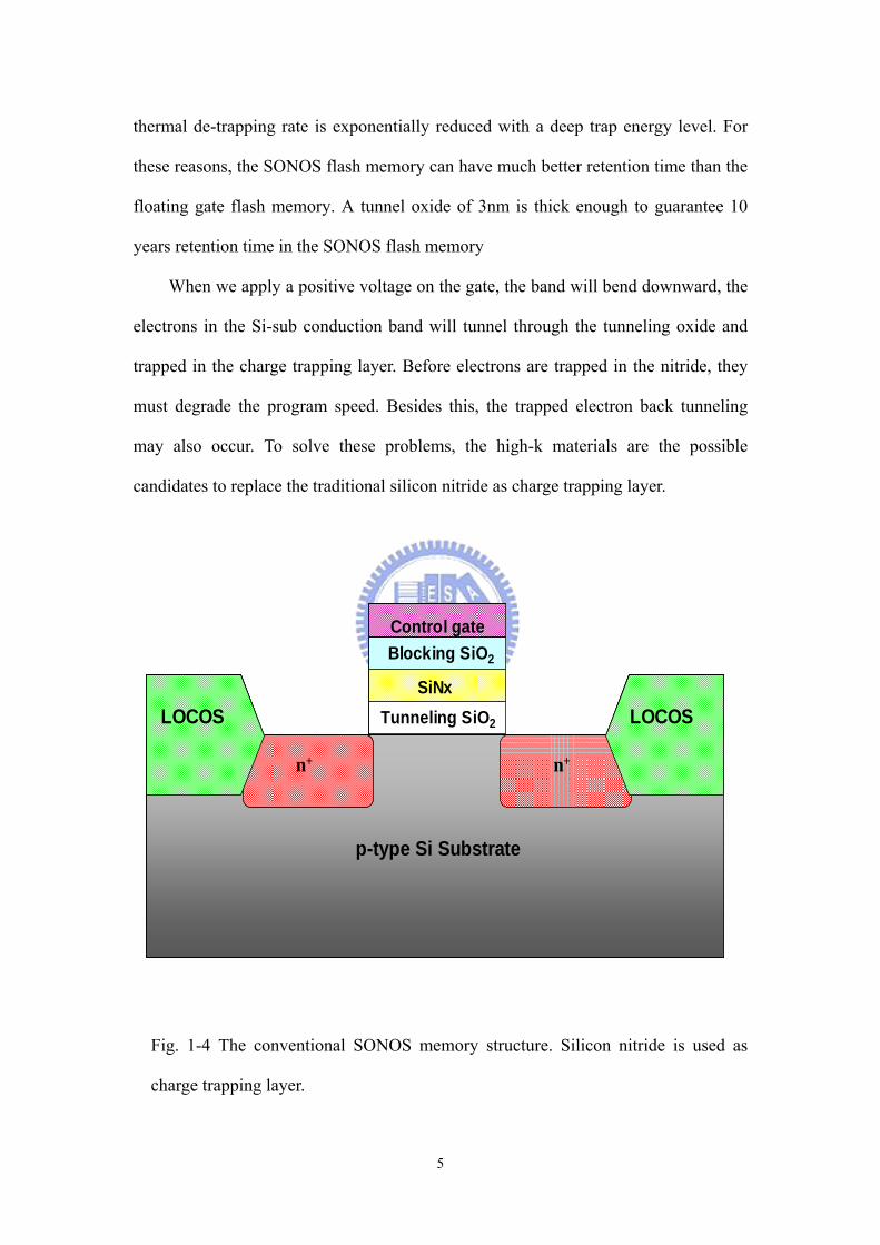
5
p-type Si Substrate
n+
LOCOS
n+
LOCOS
Control gateBlocking SiO2
Tunneling SiO2
SiNx
p-type Si Substrate
n+
LOCOS
n+
LOCOS
p-type Si Substrate
n+
LOCOS
n+n+
LOCOS
Control gateBlocking SiO2
Tunneling SiO2
SiNx
Control gateBlocking SiO2
Tunneling SiO2
SiNx
thermal de-trapping rate is exponentially reduced with a deep trap energy level For
these reasons the SONOS flash memory can have much better retention time than the
floating gate flash memory A tunnel oxide of 3nm is thick enough to guarantee 10
years retention time in the SONOS flash memory
When we apply a positive voltage on the gate the band will bend downward the
electrons in the Si-sub conduction band will tunnel through the tunneling oxide and
trapped in the charge trapping layer Before electrons are trapped in the nitride they
must degrade the program speed Besides this the trapped electron back tunneling
may also occur To solve these problems the high-k materials are the possible
candidates to replace the traditional silicon nitride as charge trapping layer
Fig 1-4 The conventional SONOS memory structure Silicon nitride is used as
charge trapping layer
6
Fig 1-5 The band diagram of nitride- based SONOS memory
The advantages of high-k material are smaller barrier height between silicon
substrate and high-k charge trapping layer and more trapping sites than silicon nitride
The smaller barrier height can get faster program speed under the same stress
condition More trapping sites can achieve larger Vth shift for larger memory window
Thus it is beneficial to use a high-k material as the charge trapping layer in a
SONOS-type memory device It provides more deep level trapping sites in the high-k
material than in silicon nitride It is desirable to choose a high-k material with small
barrier height with silicon substrate and deep trapping level as charge trapping layer
to achieve high programerase speed and good reliability due to deep trapping level
In addition high-k material has large dielectric constant a wide band gap high trap
site density so it is suitable for SONOS-type memory application
31eV
11eV
46eV
31eV
11eV
46eV
105eV
51eV
265eV
p-sub SiO2 SiO2SiN
N+ poly- Si
7
1-2 Motivation The serious leakage problem during retention can be eliminated by utilizing a
semiconductor nanocrystal memory structure Only the electrons stored on the
nanocrystal directly above the defect chain will be affected since the nanocrystals are
separated from each other within the gate oxide dielectric Hence the tunnel oxide
thickness in the nanocrystal memory device can be reduced to allow faster
programming and lower voltage operation In this thesis we have designed a high
performance nonvolatile memory with high-k CeO2 nanocrystal charge trapping layer
Use this high-k layer replace the silicon nitride layer in the SONOS structure can gain
many advantages We also use several different sourcedrain implantation approaches
to achieve superior characteristics in terms of large memory window high
programerase speed long retention time low disturbance and reduce off-state
leakage current
From the papers we find the impact of metal work function (ΦM) on memory
properties of charge-trap-flash memory devices Theoretical and experimental studies
show that high ΦM metal plays a key role in eliminating electron back tunneling (EBT)
through the blocking dielectric during the erase operation Therefore we choose
suitable temperatures to anneal different metal gates and apply these metals to
n-channel SONOS memories
1-3 Thesis Organization In this thesis we study the performance of the SONOS-type memory device
used CeO2 high-k dielectric as charge trapping layer
In Chapter 1 we introduce the background of the flash memory and explain
why SONOS-type memory with high-k charge trapping layer is studied to replace the
8
traditional floating gate memory
In Chapter 2 we fabricate MoN and TaN capacitors measuring C-V I-V and
RES characteristics And then we extract the flat band voltages of C-V curves and
metal work functions of MoN TaN under different annealing temperatures
In Chapter 3 we fabricate n-channel SONOS type memories by using CeO2
charge trapping layer And then we replace poly-Si gate with metal gate discussing
the electrical experiments The results reveal that the programerase speed and
disturbances of our devices have good characteristics
In Chapter 4 we fabricate SONOS type memory by using CeO2 charge trapping
layer and use different sourcedrain implantation approaches to achieve superior
characteristics We discuss the electrical experiments and the results reveal that the
programerase speed retention and disturbances of our devices have good
characteristics
At the end of this thesis we make a conclusion in Chapter 5
9
1-4 Reference [1] Y King ldquoThin Dielectric Technology and Memory Devicesrdquo PhD dissertation
Univ of California Berkeley CA 1999
[2] AJ Walker et al ldquo 3D TFT-SONOS Memory Cell for Ultra-High Density File
Storage Applicationsrdquo 2003 Symposium on VLSI Technology
[3] Pier Luigi Rolandi et al ldquoA 4-bitcell Flash Memory Suitable for Stand-Alone
and Embedded Mass Storage Applicationsrdquo pp75 Non-Volatile Semiconductor
Memory Workshop Monterey CA 2000
[4] ldquoAdvanced Memory Technology and Architecturerdquo short course IEDM 2001
[5] Seiichi Aritome ldquoAdvanced Flash Memory Technology and Trends for Files
Storage Applicationrdquo pp763 IEDM 2002
[6] R Bez E Camerlenghi A Modelli and A Visconti Proc of the IEEE 91 489
(2003)
[7] SM Sze ldquoPhysics of Semiconductor Devices 2nd Editionrdquo John Wiley amp Sons
[8] B D Salvo C Gerardi R V Schaijk S A Lombardo D Corso C
Plantamura T Serafino G Ammendola M V Duuren P Goarin W Y Mei
K V D Jeugd H Baron M Geacutely P Mur and S Deleonibus IEEE Trans
Device and Materials Reliability 4 377 (2004)
10
[9] Y-N Tan W-K Chim B J Cho and W-K Choi IEEE Trans Electron
Devices 51 1143 (2004)
[10] T Yamaguchi H Satake and N Fukushima IEEE Trans Electron Devices
51 774 (2004)
[11] W Zhu TP Ma T Tamagawa Y Di J Kim R Carruthers M Gibson T
Furukawa IEDM 463 (2001)
[12] S Haukka E L Lakomaa and T Suntola in Adsorption and Its Applications
in Industry and Environmental Protection Stud Surf Sci Catal ed A
Dabrowski Vol120 Elsevier Amsterdam 1998 pp 715-750
[13] S Ek Helsinki University of Technology Inorganic Chemistry Publication
Series No4 Espoo 2004
[14] C J Brinker A J Hurd P R Schunk C S Ashley R A Cairncross J
Samuel K S Chen C Scotto and R A Schwartz Metallurgical and
Ceramic Protective Coatings Chapman amp Hall London 1996 pp 112-151
[15] T Olding M Sayer and D Barrow Thin Solid Films 581(2001)
[16] T Kololuoma S M Nissila and J T Rantala Sol-Gel Optics V Society of
Photo-Optical Instrumentation 54 Engineers 2000 pp 218 (Proceedings of
SPIE Vol 3943)
[17] M Marvola J Kiesvaara K Jarvinen M Linden and A Urtti Sol-Gel
11
Derived Silica Gel Monoliths And Microparticles As Delivery in Tissue
Admonistration Division of Biopharmaceutics and Pharmacokinetics
Department of Pharmacy University of Helsinki (2001)
[18] F Schwertfeger and U Schubert Chem Mater 71909 (1995)
[19] Sanghun Jeon1 Jeong Hee Han1 Junghoon Lee1 Cheol Jong Choi2
Sangmoo Choi3 Hyunsang Hwang3 and Chungwoo Kim rdquoHigh
work-function metal gate and high-K dielectrics for charge trap flash
memorydevice applicationsrdquo Proceedings of ESSDERC Grenoble France
2005
[20] Impact of Metal Work Function on Memory Properties of Charge-Trap Flash
Memory Devices Using FowlerndashNordheim PE Mode IEEE ELECTRON
DEVICE LETTERS VOL 27 NO 6 JUNE 2006
12
Chapter 2 Physical and Electrical properties of MoN
and TaN MOS Capacitors
2-1 Introduction The problems of polysilicon (poly-Si) gate depletion high gate resistance high
gate tunneling leakage current and boron penetration into the channel region become
more severe as the channel length and gate-oxide thickness are aggressively reduced
Therefore there is immense interest in metal gates and alternative gate dielectrics
with high permittivity Metal gates with work functions near the conduction and
valence band edges of Si are desired for the N- and P-MOSFETs respectively An
accurate understanding of the top interface of the gate dielectric ie the
metalndashdielectric or the poly-Sindashdielectric interface is important to achieving precise
control of gate work functions and threshold voltages in transistors with high-k gate
dielectrics
In this work we discuss the dependence of metal gate work functions on the
different annealing temperatures We found a systematic methodology to extract the
accurate work function of metal gates This methodology consists of the interfacial
layer and decouples the impact of charges from the work function We expect metal
gate work-function can play a key role in eliminating electron back tunneling (EBT)
through the blocking dielectric during the erase operation
13
2-2 Experimental Figure 2-1 schematically depicts the process flow of the proposed MIS
capacitors The fabrication process of the MoN and TaN MOS capacitors were started
on n-type and p-type 5-10 Ω cm (100) 150mm silicon substrates First various
silicon dioxide thickness (33nm 106nm 177nm 351nm) were deposited by
chemical vapor deposition in horizontal furnace system In order to observe the effect
of metal gate work function on memory properties various metal materials on silicon
dioxide with various thicknesses were prepared Therefore MoN and TaN metals were
deposited by sputtering method with pure Mo target and pure Ta target in the nitrogen
and argon gas ambient After that the samples went through metal RTA treatment in
N2 ambient at various temperatures (500OC 600OC 700OC) for 30 sec Then all
samples went through metal RTA treatment in N2 ambient at 900OC for 20 sec Finally
the backside of the samples was deposited with Al by sputtering method with pure Al
target
Metal
SiO2
Si-substrate
IL (Interfacial layer)
Vfb=Φmsndash1 ЄOX intE
OOT xρ(x) dx
=ΦmsndashρoxEOT2 2ЄOXndashρILEOT ЄOX
0
EOTMetal
SiO2
Si-substrate
IL (Interfacial layer)
Vfb=Φmsndash1 ЄOX intE
OOT xρ(x) dx
=ΦmsndashρoxEOT2 2ЄOXndashρILEOT ЄOX
0
EOT
Fig 2-1 The process flow of the MoN and TaN MOS capacitors
2-3 Results and Discussion In this section the physical and electrical characteristics of MoN and TaN MOS
14
capacitors were discussed
Fig 2-2 shows the relation of flat band voltage and effective oxide thickness
(EOT) for TaN MOS Capacitors First we have four thicknesses of TaN MOS
capacitors annealing them at different temperatures Then we measure C-V curves
using a systematic methodology to extract the accurate flat band voltage of TaN MOS
capacitors as depicted in Fig 2-2We found three lines were intercepted in the same
point Because thermal budget of 900oC is larger than that of 500oC 600oCand 700oC
We also found that if TaN metal did not go to a pre-annealing step (such as
500oC600oC 700oC) to densify metal before treatment in N2 ambient at 900OC for 20
sec the characteristics of TaN MOS capacitors will very bad The slope of three lines
stands for effective oxide charge
0 50 100 150 200 250 300 350 400-15
-10
-05
N2 500oC 30S N2 900oC 20S
N2 600oC 30S N2 900oC 20S
N2 700oC 30S N2 900oC 20S
V fb (e
V)
EOT (A)
Fig 2-2 The relation of flat band voltage and effective oxide thickness (EOT)
under different annealing conditions for TaN MOS capacitors
15
Fig 2-3 shows the relation of flat band voltage and effective oxide thickness
(EOT) for MoN MOS Capacitors Like TaN MOS Capacitors we measure C-V curves
using a systematic methodology to extract the accurate flat band voltage of MoN
MOS capacitors as depicted in Fig 2-3 Unlike TaN MOS Capacitors if MoN metal
did not go to a pre-annealing step (such as 500oC and 600oC) to densify metal before
treatment in N2 ambient at 900OC for 20 sec the characteristics of MoN MOS
capacitors will not bad The slope of three lines stands for effective oxide charge
0 50 100 150 200 250 300 350 400 45002
03
04
05
06
07
08 N2 900oC 20S
N2 500oC 30S N2 900oC 20S
N2 600oC 30S N2 900oC 20S
V fb (e
V)
EOT (Α)
Fig 2-3 The relation of flat band voltage and effective oxide thickness (EOT)
under different annealing conditions for MoN MOS capacitors
Fig 2-4 shows work function of TaN metal and current density at Vg = 1V under
different annealing conditions From Fig 2-2 intercept at Y-axis when EOT=0 the
16
value of flat band voltage can extract work function of TaN It shows almost the same
work function value The right Y-axis show the current density at Vg = 1V TaN
metal did not go to a pre-annealing step (such as 500oC 600oC 700oC) to densify
metal before treatment in N2 ambient at 900OC for 20 sec which has the maximum
leakage current density Another TaN metal went to a 700oC pre-annealing step
which has the minimum leakage current density
As 500 600 70043
44
45
46
47
EOT = 338 nmAnneal at 900oC in N2 for 20 sJ measured at Vg = 1 V
Current D
ensity J (Acm
2)
Wor
k fu
nctio
n (e
V)
Pre-annealed Temperature (OC)
1E-6
1E-5
1E-4
Fig 2-4 Work function of TaN metal and current density at Vg = 1V under
different annealing conditions
Fig 2-5 shows work function of MoN metal and current density at Vg = -1V
under different annealing conditions From Fig 2-3 intercept at Y-axis when EOT=0
the value of flat band voltage can extract work function of MoN The metal work
17
function value ranges about 01eV (about 49eV~5eV) The right Y-axis show the
current density at Vg = -1V MoN metal went to a 500oC pre-annealing step to
densify metal before treatment in N2 ambient at 900OC for 20 sec which has the
maximum leakage current density Another MoN metal went to a 600oC
pre-annealing step which has the minimum leakage current density
As 500 600 47
48
49
50
EOT = 338 nmAnneal at 900oC in N2 for 20 sJ measured at Vg = - 1 V
Current D
ensity J (Acm
2)
Wor
k fu
nctio
n (e
V)
Pre-annealed Temperature (OC)
1E-7
1E-6
1E-5
1E-4
As 500 600 47
48
49
50
EOT = 338 nmAnneal at 900oC in N2 for 20 sJ measured at Vg = - 1 V
Current D
ensity J (Acm
2)
Wor
k fu
nctio
n (e
V)
Pre-annealed Temperature (OC)
1E-7
1E-6
1E-5
1E-4
Fig 2-5 Work function of MoN metal and current density at Vg = - 1V under
different annealing conditions
From the above pictures we plot a table to show work function and current
density for different metal and annealing conditions As depicted in Table2-1
18
900E-074622700rarr900TaN
153E-064622600rarr900TaN
254E-054601500rarr900TaN
901E-07497600rarr900MoN
459E-054879500rarr900MoN
999E-07495ASrarr900MoN
Jg atV=1V(Acm-2)
WF(eV)
Condition( OC )
Material
900E-074622700rarr900TaN
153E-064622600rarr900TaN
254E-054601500rarr900TaN
901E-07497600rarr900MoN
459E-054879500rarr900MoN
999E-07495ASrarr900MoN
Jg atV=1V(Acm-2)
WF(eV)
Condition( OC )
Material
Table 2-1 Work function and current density for TaN and MoN metal
2-4 Summary In this chapter we found the work function of TaN was about 46eV It located at
the midgap of energy level so we choose a 700oC pre-annealing step to densify metal
and then treatment at 900OC for 20 sec to fabricate NMOS and PMOS In the other
hand for MoN metal we choose a 600oC pre-annealing step to densify metal and then
treatment at 900OC for 20 sec to fabricate NMOS
19
2-5 Reference
[1] ldquoEffects of High-K Gate Dielectric Materials on Metal and Silicon Gate
Workfunctionsrdquo Yee-Chia Yeo Student Member IEEE Pushkar Ranade
Student Member IEEE Tsu-Jae King Senior Member IEEE and Chenming Hu
Fellow IEEE IEEE ELECTRON DEVICE LETTERS VOL 23 NO 6 JUNE
2002
[2] A Capacitance-Based Methodology for Work Function Extraction of Metals on
High-K Rashmi Jha Jason Gurganos Y H Kim R Choi Jack Lee Member
IEEE and Veena Misra Member IEEE IEEE ELECTRON DEVICE
LETTERS VOL 25 NO 6 JUNE 2004
[3] High work-function metal gate and high-K dielectrics for charge trap flash
memory device applications Sanghun Jeon1 Jeong Hee Han1 Junghoon
Lee1 Cheol Jong Choi2 Sangmoo Choi3 Hyunsang Hwang3 and Chungwoo
Kim Proceedings of ESSDERC Grenoble France 2005
[4] The impact of work-function of metal gate and fixed oxide charge of high-K
blocking dielectric on memory properties ofNAND type charge trap flash
memory devices Sanghun Jeonl Jeong Hee Hani Junghoon Lee1 Jaewoong
Hyun Ju Hyung Kim2 Y S Jeong Hee Soon Chael Soo Doo Chae2 M K
Kim J-W Leel Sangmoo Choi3 Man Jang3 Hyunsang Hwang3 and
Chungwoo Kim1
20
[5] Thermal Instability of Effective Work Function in MetalHigh-K Stack and Its
Material Dependence Moon Sig Joo Byung Jin Cho Senior Member IEEE N
Balasubramanian and Dim-Lee Kwong Senior Member IEEE IEEE
ELECTRON DEVICE LETTERS VOL 25 NO 11 NOVEMBER 2004
21
Chapter 3
Characteristics of High-K CeO2 Nanocrystal
Memory with Different Metal Gates
3-1 Introduction
Charge trapping flash(CTF) memory devices have received considerable attention
due to the detrimental coupling effect among adjacent cells in sub-50nm NAND type
floating gate flash memory devices Nitride based CTF memory devices have several
advantages such as fast programming low power operation high density integration
good reliability characteristics and high compatibility with conventional CMOS
technology However it is difficult to satisfy the NAND specifications of low erase state
Vth of ndash3V from 1V at ndash18V for 2ms and good retention characteristics because the
current through the tunnel dielectric thickness critically affects both properties and the
electron back tunneling (EBT) during erase operation limits the low erase state Vth EBT
is known to a serious concern for meeting specification of NAND devices using
Fowler-Nordheim (FN) program and erase schemes The experimental studies show that
high work-function metal gate and high permittivity (high-K) dielectric play a key role in
eliminating electron back tunneling (EBT) through the blocking dielectric during the
erase operation
In this work in order to reconcile this conflicting behavior we have carried out a
study on the impact of work function of metal gate and high permittivity (high-K)
dielectric on the memory properties of CeO2 based CTF devices Techniques to improve
erase efficiency of CTF memory devices with different metal gates by using n-channel
CeO2 based CTF devices are discussed In the past n-channel flash cells were widely
used in the design of flash memory products However the requirement of high voltage
operation for channel-hot-electron (CHE) programming results in a large power
consumption In order to improve it the p-channel flash cell has been suggested for low
22
voltage and low power applications A more matured p-channel cell using band-to-hand
tunneling induced hot electron injection (BBHE) has later been proposed We
demonstrate reliability enhancement for n-channel and p-channel flash cells
3-2 Experimental Figure 4-1 schematically depicts the process flow of the proposed SONOS flash
memory The fabrication process of the CeO2 nanocrystal memory devices involved was
started with the LOCOS isolation process on p-type and n-type 5-10 Ω cm (100) 150mm
silicon substrates First a 3 nm thick tunnel oxide was thermally grown at 1000OC in
vertical furnace system The trapping layer of CeO2 layer was deposited by dual E-gun
method with CeO2 target After that the samples went through RTA treatment in O2
ambient at 900OC for 1 minute A blocking oxide of about 20 nm thick was then
deposited by high density plasma chemical vapor deposition (HDPCVD) After that the
sample went through RTA treatment in O2 ambient at 900OC for 1 minute For control
samples a 200 nm thick poly-silicon was deposited to serve as the gate electrode by
LPCVD In addition another metal gates 100nm MoN and TaN were deposited by
sputtering method with pure Mo target and pure Ta target in the nitrogen and argon gas
ambient Then gate electrode was patterned For NMOSFET the sourcedrain and gate
were doped by self-aligned P ion implantation at the dosage and energy of 5times1015
ionscm-2 and 25 KeV then the substrate contact was patterned and the sub-contact was
implanted with BF2 at the dosage and energy of 5times1015 ionscm-2 and 40 KeV For
PMOSFET the sourcedrain and gate were doped by self-aligned BF2 ion implantation at
the dosage and energy of 5times1015 ionscm-2 and 25 KeV then the substrate contact was
patterned and the sub-contact was implanted with P at the dosage and energy of 5times1015
ionscm-2 and 40 KeV After these implantations for NMOSFET the dopants were
activated at 950OC for 20 sec For PMOSFET the dopants were activated at 950OC for 10
sec The rest of the subsequent standard CMOS procedures were complete for fabricating
the CeO2 high-k memory devices
23
p-type Si substrate
LOCOSLOCOS
p-type Si substrate
LOCOSLOCOS
p-type Si substrate
LOCOSLOCOSTunneling oxide
p-type Si substrate
LOCOSLOCOSTunneling oxide
p-type Si substrate
LOCOSLOCOSTunneling oxide
CeO2 Trapping layer
p-type Si substrate
LOCOSLOCOSTunneling oxide
CeO2 Trapping layer
O2 RTA 900OC 60secform CeO2 nanocrystal
24
p-type Si substrate
LOCOSLOCOSTunneling oxide
CeO2 nanocrystalBlocking oxide
p-type Si substrate
LOCOSLOCOSTunneling oxide
CeO2 nanocrystalBlocking oxide
p-type Si substrate
LOCOSLOCOSTunneling oxide
CeO2 nanocrystal
Metal Gate
Blocking oxide
p-type Si substrate
LOCOSLOCOSTunneling oxide
CeO2 nanocrystal
Metal Gate
Blocking oxide
25
p-type Si substrate
Tunneling oxideCeO2 nanocrystal
Blocking Oxide
Metal Gate
LOCOSLOCOS
p-type Si substrate
Tunneling oxideCeO2 nanocrystal
Blocking Oxide
Metal Gate
LOCOSLOCOS
p-type Si substrate
Tunneling oxideCeO2 nanocrystal
Blocking Oxide
Metal Gate
LOCOSLOCOS
P31+ Ion implantation
p-type Si substrate
Tunneling oxideCeO2 nanocrystal
Blocking Oxide
Metal Gate
LOCOSLOCOS
p-type Si substrate
Tunneling oxideCeO2 nanocrystal
Blocking Oxide
Metal Gate
LOCOSLOCOSLOCOSLOCOS
P31+ Ion implantation
26
p-type Si substrate
Tunneling oxideCeO2 nanocrystal
Blocking Oxide
Metal Gate
LOCOSLOCOS N+N+
p-type Si substrate
Tunneling oxideCeO2 nanocrystal
Blocking Oxide
Metal Gate
LOCOSLOCOS N+N+
p-type Si substrate
Tunneling oxideCeO2 nanocrystal
Blocking Oxide
Metal Gate
LOCOSLOCOS
metal
N+ N+
SiO2
p-type Si substrate
Tunneling oxideCeO2 nanocrystal
Blocking Oxide
Metal Gate
LOCOSLOCOS
p-type Si substrate
Tunneling oxideCeO2 nanocrystal
Blocking Oxide
Metal Gate
LOCOSLOCOS
p-type Si substrate
Tunneling oxideCeO2 nanocrystal
Blocking Oxide
Metal Gate
LOCOSLOCOS
metal
N+ N+
SiO2
Fig 3-1 The process flow of the metal gate flash memory and the cross-section of
the metal gate flash memory
27
3-3 Results and Discussion In this section the electrical characteristics of metal gate high-k CeO2 nanocrystal
SONOS-type memory were discussed
3-3-1 Id-Vg Curve
0 1 2 3 4 5 6 7 8 910-1310-1210-1110-1010-910-810-710-610-510-410-310-2
Fresh Program state Vg=7V Vd=7V 1msec Erase state Vg=- 3V Vd=8V 1msec
I d (A)
Vg (V)
Fig 3-2 The Id-Vg curves of the MoN metal gate flash memory in the
programmed and erased state
Figure 3-2 shows the Id-Vg curve of the device under program and erase operations
We use channel hot electron injection (CHEI) to program and band to band hot hole to
erase (BTBHH) The program condition is Vg= 7V Vd= 7V with 1 msec stress The erase
condition are Vg= -3V Vd= 8V with 1 msec stress The Vth after programming shifts
28
about 2V from the original fresh state After erasing the Vth shifts leftward 19V So the
memory window is about 2V
-2 -1 0 1 2 3 4 5 6 710-12
10-11
10-10
10-9
10-8
10-7
10-6
10-5
10-4
10-3 Fresh Erase state Vg= - 3V Vd=9V 1msec Program state Vg=7V Vd=7V 1msec
I d (A
)
Vg (V)
Fig 3-3 The Id-Vg curves of the TaN metal gate flash memory in the
programmed and erased state
Figure 3-3 shows the Id-Vg curve of the device under program and erase operations
We use CHEI to program and BTBHH to erase The program condition is Vg= 7V Vd=
7V with 1 msec stress The erase condition are Vg= -3V Vd= 9V with 1 msec stress The
memory window is about 2V
3-3-2 Program and Erase Speed
29
For the high-k CeO2 nanocrystal SONOS-type flash memory with MoN metal gate
the program speed is shown in Fig3-4
10-7 10-6 10-5 10-4 10-3 10-2 10-1 100
0
1
2
3
4
5 Vg=6V Vd=6V Vg=7V Vd=7V Vg=8V Vd=8V Vg=9V Vd=9V
V th s
hift
(V)
Program Time (sec)
Fig 3-4 The program speed curves of high-k CeO2 nanocrystal SONOS-type
flash memory with MoN metal gate
We show four different stress conditions Vg=6VVd=6V Vg=7VVd=7V
Vg=8VVd=8V Vg=9VVd=9V As Fig 3-4 shows the condition Vg=7V Vd=7V 1
msec cause Vth shift about 2V and the condition Vg=8V Vd=8V 01 msec cause Vth
shift over 2V Its memory window is gt 4V At large voltage (such as gt Vg=9V Vd =9)
the program speed is very fast within short time Like the condition Vg=9V Vd =9V 1
usec cause Vth shift 23V
30
10-7 10-6 10-5 10-4 10-3 10-2 10-1 100
0
1
2
3
Initial Vt
Vg=-3V Vd=8V Vg=-4V Vd=8V Vg=-5V Vd=8V
V th
shi
ft (V
)
Erase Time (sec)
Fig 3-5 The erase speed curves of high-k CeO2 nanocrystal SONOS-type flash
memory with MoN metal gate
Figure 3-5 shows the erase speed of the MoN metal gate device For Vg= -3V -4V
and -5V with the same Vd =8V We can see all stress conditions the Vth shift gt 2V in
10msec The final erase state is below the initial state Therefore it shows no electron
back tunneling (EBT) and a little over-erase
For the high-k CeO2 nanocrystal SONOS-type flash memory with TaN metal gate
the program speed is shown in Fig3-6 We show three different stress conditions Vg=5V
Vd=5V Vg=6V Vd=6V Vg=7V Vd=7V As Fig 3-6 shows the condition Vg=7V Vd
=7V 1 msec cause Vth shift about 2V Its memory window is gt 5V
31
10-7 10-6 10-5 10-4 10-3 10-2 10-1 100
0
1
2
3
4
5 Vg=5V Vd=5V Vg=6V Vd=6V Vg=7V Vd=7V
V th
shi
ft (V
)
Program Time (sec)
Fig 3-6 The program speed curves of high-k CeO2 nanocrystal SONOS-type
flash memory with TaN metal gate
Figure 3-7 shows the erase speed of the TaN metal gate device For Vg= -3V -4V
and -5V with the same Vd=9V We can see all stress conditions the Vth shift gt 2V in
10msec And Vt shift of -2V can be achieved with Vg=-4 Vd=9V t lt1ms The final erase
state is below the initial state Because it has no electron back tunneling (EBT) so it
shows over-erase under large erase voltage (such as Vg= -4V Vd=9V and Vg=
-5V Vd=9V)
32
10-7 10-6 10-5 10-4 10-3 10-2 10-1 100-1
0
1
2
3
Initial Vt
Vg=-3V Vd=9V Vg=-4V Vd=9V Vg=-5V Vd=9V
V th
shi
ft (V
)
Erase Time (sec)
Fig 3-7 The erase speed curves of high-k CeO2 nanocrystal SONOS-type flash
memory with TaN metal gate
Figure 3-8 shows the erase speed of the N+-poly and MoN metal gate device To be
clearly understood EBT phenomenon we use F-N tunneling mechanism to erase For
N+-poly gate we can see a little Vth shift under small voltage (Vg=-15V) And EBT
phenomenon occurs when we apply large voltage to it (Vg=-18V) For MoN metal gate
it has no EBT under whether large nor small voltage It shows reasonable erase speed for
MoN metal gate device
33
10-7 10-6 10-5 10-4 10-3 10-2 10-1 1002
3
4
5
6
7
8 N+- poly gate Vg=-15V Vg=-18V
MoN gate Vg=-15V Vg=-18V
V th
shi
ft(V)
Erase Time(sec)
initial Vt
Fig 3-8 The erase speed curves of N+-poly and MoN gate CeO2 nanocrystal
memory with F-N tunneling mechanism
3-3-3 Data Retention Characteristic
Fig 3-9 is the data retention characteristic of MoN metal gate high-k CeO2
nanocrystal SONOS memory measured at 25oC We find the small charge loss with
time The curve shows only 5 charge loss as measure time up to 104 sec and 13
charge loss up to 108 sec at 25oC We infer the small charge loss at room temperature is
from the electron deep trap of high-k CeO2 nanocrystal We prove that sputtering MoN
and TaN metal will not damage the blocking oxide and CeO2 layer so it shows good
retention characteristic
34
100 101 102 103 104 105 106 107 1080
1
2
3
4
5
6
Initial Vt
retention at T=25oC
V th
(V)
Time (sec)
Fig 3-9 Retention characteristic of MoN metal gate high-k CeO2 nanocrystal
SONOS-type flash memory at 25OC
3-3-4 Disturbance Measurement Figure 3-10 shows the gate disturbance measurement of the MoN metal gate device
for three stress conditions Vg=7V Vg= 9V and Vg=11V with Vd =Vs=Vb=0V And
Figure 3-11 shows the gate disturbance measurement of the TaN metal gate device for
three stress conditions Vg=6V Vg= 8V and Vg=10V with Vd =Vs=Vb=0V The applied
gate voltage will attract electrons in the substrate tunneling to the CeO2 layer by FN
tunneling mechanism and result into Vth increase After 1000 sec stress the fresh state
Vth are almost the same It shows almost no gate disturbance after 1000 sec stress
35
100 101 102 103-2
-1
0
1
2
MoN Metal Vg=7V Vg=9V Vg=11V
Er
ase
stat
e V th
shi
ft (V
)
Gate Disturb Time (sec)
Fig 3-10 The gate disturbance characteristics of MoN metal gate device
100 101 102 103-20
-15
-10
-05
00
05
10
15
20
TaN Metal Vg=6V Vg=8V Vg=10V
Eras
e st
ate
V th s
hift
(V)
Gate Disturb Time (sec)
Fig 3-11 The gate disturbance characteristics of TaN metal gate device
36
Figure 3-12 shows the read disturbance measurement of the MoN metal gate device
And Figure 3-13 shows the read disturbance measurement of the TaN metal gate device
The measurement conditions are all fixed Vg=4V with different Vd= 2V 3V and 4V for
1000 sec stress The stress caused the fresh state Vth increase almost 0V It shows almost
no read disturbance after 1000 sec stress
100 101 102 103-2
-1
0
1
2
MoN Metal Vg=4V Vd=2V Vg=4V Vd=3V Vg=4V Vd=4V
Eras
e st
ate
V th s
hift
(V)
Read Disturb Time (sec)
Fig 3-12 The read disturbance characteristics of MoN metal gate device
37
100 101 102 103-2
-1
0
1
2
TaN Metal Vg=4V Vd=2V Vg=4V Vd=3V Vg=4V Vd=4V
Er
ase
stat
e V th
shi
ft (V
)
Read Disturb Time (sec)
Fig 3-13 The gate disturbance characteristics of TaN metal gate device
3-3-5 Physical Characteristics
Fig 3-14 shows the X-ray diffraction (XRD) characteristic of MoN metal gate
device The incident angle ranges from 15 degree to 60 degree We find signal intensity
peak appears at 3285 degree By searching the data base we find the rate between Mo
and N element is 11
Fig 3-15 shows the X-ray diffraction (XRD) characteristic of TaN metal gate device
The incident angle ranges from 15 degree to 60 degree We find signal intensity peak
appears at 33 degree By searching the data base we find the rate between Ta and N
element is 2086
38
20 30 40 50 600
500
1000
1500
2000
XRD Mo1N1
In
tens
ity (c
ps)
2 THETA (deg)
3285
Fig 3-14 The XRD characteristic of MoN metal gate device
28 30 32 34 36 380
5000
10000
15000
20000
XRD Ta2N086
Inte
nsity
(cps
)
2 THETA (deg)
33
Fig 3-15 The XRD characteristic of TaN metal gate device
39
Fig 3-16 The TEM image of MoN metal gate device
Fig 3-16 shows the cross-section-view high resolution tunneling electron
microscopy (HRTEM) of MoN metal gate device From the image the isolation of the
nanocrystals prevents the formation of effective conductive paths between adjacent nodes
The thickness of the tunnel oxide and blocking oxide are about 34nm and 154nm and
the thickness of the MoN metal is about 932nm The nanocrystal size ranges from 75nm
to 98nm
40
3-4 Summary In this chapter we replace conventional poly-Si gate with metal gate MoN TaN We
have shown the electric curves like Id-Vg program speed erase speed and small
disturbance We improve erase efficiency of high-k CeO2 nanocrystal memory with
different metal gates by using p-channel and n-channel devices We also demonstrate the
quality of high-k CeO2 nanocrystal with some good characteristics
41
3-5 Reference [1] Marvin H White Yang (Larry) Yang Ansha Purwar Margaret L Frenchrdquo A Low
Voltage SONOS Nonvolatile Semiconductor Memory Technology rdquo IEEE
transactions on components packaging and manufacturing technologymdashPART A
VOL 20 NO 2 JUNE 1997
[2] Shin-ichi Minami and Yoshiaki Kamigakirdquo A Novel MONOS Nonvolatile Memory
Device Ensuring 10-Year Data Retention after 107 EraseWrite Cycles rdquo IEEE
Transactions on Electron Devices VOL 40 NO 11 NOVEMBER 1993
[3] C C-H Hsu et al Exf Ah SSDM Tsukuba p 1401992
[4] T Ohnakado et al in IEDM Tech Dig p 2791995
[5] Jao-Hsian Shiue et al A study of interface trap generation by Fowler-Nordheim
and Substrate-hot-carrier stresses for 4-nm thick gate oxides in IEEE transactions
on electron devices vol 46 NO8 August 1999
[6] O Takahiro T Hiroshi K Hayashi and M D K Kaisha ldquoNon-volatile
semiconductor memory device capable of high speed programmingerasure US
patent no 5818761rdquo Oct 6 1998
[7] D P Shum et al ldquoA novel band-to-band tunneling induced convergence
mechanism for low current high density Flash EEPROM applicationsrdquo in IEDM
Tech Dig 1994 pp 41ndash44
[8] C-Y Hu et al ldquoSubstrate-current-induced hot electron (SCIHE) injection A new
convergence scheme for Flash memoryrdquo in IEDM Tech Dig 1995 pp 283ndash287
[9] T S Chen K H Wu H Chung and C H Kao ldquoperformance improvement of
SONOS memory by bandgap engineer of charge-trapping layerldquo IEEE Electron
42
Device Lett vol25 no4 pp 205-207 Apr 2002
[10] Marvin H White Yang (Larry) Yang Ansha Purwar Margaret L Frenchrdquo A
Low Voltage SONOS Nonvolatile Semiconductor Memory Technology rdquo IEEE
transactions on components packaging and manufacturing technologymdashPART A
VOL 20 NO 2 JUNE 1997
[11] T Sugizaki M Kohayashi M Ishidao H Minakata M Yamaguchi Y Tamura
Y Sugiyama T Nakanishi and H Tanakardquo Novel Multi-bit SONOS Type Flash
Memory Using a Highk Charge Trapping Layerrdquo Symposium on VLSl Technology
Digest of Technical Papers 2003
[12] Marvin H White Dennis A Adams James R Murray StephenWrazien Yijie
(Sandy) Zhao Yu (Richard) Wang Bilal Khan Wayne Miller Rajiv Mehrotra1rdquo
Characterization of Scaled SONOS EEPROM Memory Devices for Space and
Military Systems rdquo IEEE 2004
[13] G D Wilk R M Wallace J M Anthony rdquoHigh-k gate dielectrics Current status
and materials properties considerations rdquo Applied Physics Review vol89
no10pp5243-5275 Nay 2001
[14] T Ohnakado et al ldquoNovel electron injection method using band-to-band
tunneling induced hot electron (BBHE) for Flash memory with a p-channel cellrdquo
IEDM Tech Dig pp 279ndash282 1995
[15] T Ohnakado et al ldquoNovel self-limiting program scheme utilizing N-channel
select transistors in P-channel DINOR Flash memoryrdquo in IEDM Tech Dig 1996
pp 181ndash184
[16] S J Shen C S Yang Y S Wang and C C-H HsuldquoNovel self-convergent
programming scheme for multilevel P-channel Flash memoryrdquo in IEDM Tech
43
Dig 1997 pp 287ndash290
[17] R-L Lin Y-S Wang and C C-H HsuldquoP-channel Flash memoryrdquo in Proc
NVSMW 1998 pp 27ndash34
[18] T S-D Chang ldquoPMOS memory cell with hot electron injection programming and
tunneling erasing US Patent no 5687118rdquo Nov 11 1997
[19] T S-D Chang ldquoPMOS flash memory cell capable of multi-level threshold
voltage storage US Patent no 5666307rdquo Sept 9 1997
[20] T S-D Changldquonon-volatile electrically erasable memory with PMOS transistor
NAND gate structure US Patent no 5581504rdquo Dec 3 1996
[21] S J Shen C S Yang Y S Wang and C C-H HsuldquoNovel self-convergent
programming scheme for multilevel P-channel Flash memoryrdquo in IEDM Tech
Dig 1997 pp 287ndash290
[22] Frank Ruei-Ling Lin Yen-Sen Wang and Charles Ching-Hsiang Hsu
ldquoMulti-Level P-channel Flash Memoryrdquo pp457-463
[23] Steve S Chung S N Kuo C M Yih and T S Chao ldquoPerformance and
Reliability Evaluations of P-Channel Flash Memories with Different Programming
Schemesrdquo IEDM 97-295
[24] C C-H Hsu et al ldquoA high speed low power p-channel Flash EEPROM using
silicon rich oxide as tunneling dielectricrdquo in Proc Conf Solid State Devices and
Materials 1992 pp 140ndash141
44
Chapter 4
Characteristics of High-K CeO2 Nanocrystal
Memory with Different SourceDrain
Implantations
4-1 Introduction Recently SONOS-type memory has received considerable interest as one of the most
promising candidates to replace the conventional floating-gate flash memory Because as
the tunnel oxide thickness is scaled below 80 Aring the stress-induced leakage current (SILC)
has become such a severe problem that it will be a formidable challenge for floating-gate
devices to meet the ten-year retention requirement However for the SONOS device due
to its discrete charge trapping nature it is more robust to SILC since there is no lateral
charges movement to discharge the whole memory as one single defect is generated in
the tunnel oxide In addition SONOS memory has low operation voltage better
endurance and good compatibility with conventional CMOS process However
achieving fast programming and long retention at the same time remains to be one
challenge for SONOS devices Various approaches have been proposed for improving the
SONOS performance and reliability
In this work we purpose a high performance nonvolatile memory with high-k CeO2
nanocrystal charge trapping layer The serious leakage problem during retention can be
eliminated by utilizing a nanocrystal memory structure The electrons stored on the
nanocrystal directly above the defect chain will be affected since the nanocrystals are
separated from each other within the gate oxide dielectric The tunnel oxide thickness in
the nanocrystal memory device can be reduced to allow faster programming and lower
voltage operation We also use different sourcedrain implantation approaches to achieve
superior memory characteristics
45
4-2 Experimental Figure 4-1 schematically depicts the process flow of the proposed SONOS flash
memory
p-type Si substrate
LOCOSLOCOS
p-type Si substrate
LOCOSLOCOS
p-type Si substrate
LOCOSLOCOSTunneling oxide
CeO2 nanocrystal
Poly-Si Gate
Blocking oxide
p-type Si substrate
LOCOSLOCOSTunneling oxide
CeO2 nanocrystal
Poly-Si Gate
Blocking oxide
46
p-type Si substrate
Tunneling oxideCeO2 nanocrystal
Blocking Oxide
Poly-Si Gate
LOCOSLOCOS N+N+
p-type Si substrate
Tunneling oxideCeO2 nanocrystal
Blocking Oxide
Poly-Si Gate
LOCOSLOCOS N+N+
p-type Si substrate
Tunneling oxideCeO2 nanocrystal
Blocking Oxide
Poly-Si Gate
LOCOSLOCOS
metal
N+ N+
SiO2
p-type Si substrate
Tunneling oxideCeO2 nanocrystal
Blocking Oxide
Poly-Si Gate
LOCOSLOCOS
p-type Si substrate
Tunneling oxideCeO2 nanocrystal
Blocking Oxide
Poly-Si Gate
LOCOSLOCOS
p-type Si substrate
Tunneling oxideCeO2 nanocrystal
Blocking Oxide
Poly-Si Gate
LOCOSLOCOS
metal
N+ N+
SiO2
47
Fig 4-1 The process flow of the flash memory and the cross-section of the flash
memory (control samples)
The fabrication process of the CeO2 nanocrystal memory devices involved was
started with the LOCOS isolation process on p-type 5-10 Ω cm (100) 150mm silicon
substrates First a 2 nm thick tunnel oxide was thermally grown at 1000OC in vertical
furnace system The trapping layer of CeO2 layer was deposited by dual E-gun method
with CeO2 target After that the samples went through RTA treatment in O2 ambient at
900OC for 1 minute A blocking oxide of about 20 nm thick was then deposited by high
density plasma chemical vapor deposition (HDPCVD) After that the sample went
through RTA treatment in O2 ambient at 900OC for 1 minute Then a 200 nm thick
poly-silicon was deposited to serve as the gate electrode by LPCVD Then gate electrode
was patterned and the sourcedrain and gate were doped by self-aligned P ion
implantation at the dosage and energy of 5times1015 ionscm-2 and 25 KeV then the substrate
contact was patterned and the sub-contact was implanted with BF2 at the dosage and
energy of 5times1015 ionscm-2 and 40 KeV After these implantations the dopants were
activated at 950OC for 20 sec The rest of the subsequent standard CMOS procedures
were complete for fabricating the CeO2 high-k memory devices The above are control
samples
48
p-type Si substrate
Tunneling oxideCeO2 nanocrystal
Blocking Oxide
Poly-Si Gate
LOCOSLOCOS
BF2 ion implantation
p-type Si substrate
Tunneling oxideCeO2 nanocrystal
Blocking Oxide
Poly-Si Gate
LOCOSLOCOS
p-type Si substrate
Tunneling oxideCeO2 nanocrystal
Blocking Oxide
Poly-Si Gate
LOCOSLOCOS
BF2 ion implantation
p-type Si substrate
Tunneling oxideCeO2 nanocrystal
Blocking Oxide
Poly-Si Gate
LOCOSLOCOS
P31+ ion implantation
p-type Si substrate
Tunneling oxideCeO2 nanocrystal
Blocking Oxide
Poly-Si Gate
LOCOSLOCOSLOCOSLOCOS
P31+ ion implantation
49
p-type Si substrate
Tunneling oxideCeO2 nanocrystal
Blocking Oxide
Poly-Si Gate
LOCOSLOCOS N+N+ P+
p-type Si substrate
Tunneling oxideCeO2 nanocrystal
Blocking Oxide
Poly-Si Gate
LOCOSLOCOS N+N+ P+
p-type Si substrate
Tunneling oxideCeO2 nanocrystal
Blocking Oxide
Poly-Si Gate
LOCOSLOCOS
metal
N+ N+P+
SiO2
p-type Si substrate
Tunneling oxideCeO2 nanocrystal
Blocking Oxide
Poly-Si Gate
LOCOSLOCOS
p-type Si substrate
Tunneling oxideCeO2 nanocrystal
Blocking Oxide
Poly-Si Gate
LOCOSLOCOS
metal
N+ N+P+
SiO2
Fig 4-2 The process flow and the cross-section of the asymmetry sourcedrain
50
flash memory (asymmetry SD)
Figure 4-2 schematically depicts the process flow of the asymmetry sourcedrain
SONOS flash memory We changed the sourcedrain implantation with BF2 ion
implantation at the dosage and energy of 5times1013 ionscm-2 and 25 KeV (twist angle 72
degree tilt angle 30degree) then doped by P ion implantation at the dosage and energy
of 5times1015 ionscm-2 and 25 KeV (twist angle 0 degree tilt angle 0 degree) Then the
substrate contact was patterned and the sub-contact was implanted with BF2 at the dosage
and energy of 5times1015 ionscm-2 and 40 KeV After these implantations the dopants were
activated at 950OC for 20 sec The rest of the subsequent standard CMOS procedures
were complete for fabricating the CeO2 high-k memory devices
4-3 Results and Discussion In this section the electrical characteristics of high-k CeO2 nanocrystal SONOS-type
memory were discussed
4-3-1 Id-Vg Curve Figure 4-3 shows the Id-Vg curves of the device under program and erase
operations
51
2 3 4 5 6 7 8 9 101E-12
1E-11
1E-10
1E-9
1E-8
1E-7
1E-6
1E-5
1E-4
1E-3 Fresh Program state Vg=7V Vd=7V 10msec Erase state Vg=-4V Vd=8V 10msec
I d (A
)
Vg (V)
Fig 4-3 The Id-Vg curves of the high-k CeO2 nanocrystal SONOS-type flash
memory in the programmed and erase state
We use channel hot electron injection (CHEI) to program and band to band hot hole
to erase (BTBHH) The program condition is Vg= 7V Vd= 7V with 10 msec stress The
erase condition are Vg= -4V Vd= 8V with 10 msec stress The Vth after programming
shifts about 3V from the original fresh state After erasing the Vth shifts leftward about
27V So the memory window is about 3V We think the Vth shift rightward is due to
electron trapping in the high-k CeO2 nanocrystal layer The band offset is the reason why
trapping occurred During programming the electrons in the substrate gain energy from
the applied voltage Vg and Vd If the energy is enough to cross the energy barrier the hot
electrons will inject to the high-k CeO2 nanocrystal charge trapping layer and be trapped
This causes the Vth change When erasing we apply a negative gate voltage and positive
52
drain voltage to generate hot hole in the substrate If the hot hole in the substrate achieves
enough energy to cross the energy barrier it can reach the high-k CeO2 nanocrystal
charge trapping layer and cause the Id-Vg curve shift toward left
0 1 2 3 4 5 6 7 810-12
10-11
10-10
10-9
10-8
10-7
10-6
10-5
10-4
10-3
Fresh Program state Vg=7V Vd=7V 1msec Erase state Vg=-4V Vd=8V 10msec
I d (A
)
Vg (V)
Fig 4-4 The Id-Vg curves of the asymmetry sourcedrain high-k CeO2
nanocrystal SONOS-type flash memory
Figure 4-4 shows the Id-Vg curves of the device under program and erase operations
We use channel hot electron injection (CHEI) to program and band to band hot hole to
erase (BTBHH) The program condition is Vg= 7V Vd= 7V with 1 msec stress The erase
condition are Vg= -4V Vd= 8V with 10 msec stress The Vth after programming shifts
about 23V from the original fresh state After erasing the Vth shifts leftward about 23V
So the memory window is about 23V
4-3-2 Program and Erase Speed
53
For the control samples the program speed is shown in Fig 4-5
10-7 10-6 10-5 10-4 10-3 10-2 10-1 100
0
1
2
3
4
5
6 Vg=6V Vd=6V Vg=7V Vd=7V Vg=8V Vd=8V Vg=9V Vd=9V
V th s
hift
(V)
Program Time(sec)
Fig 4-5 The program speed curve of high-k CeO2 nanocrystal SONOS-type flash
memory
We show four different stress conditions Vg=6VVd=6V Vg=7VVd=7V
Vg=8VVd=8V Vg=9VVd=9V As Fig 4-5 shows the condition Vg=7V Vd=7V 1
msec cause Vth shift 2V and the condition Vg=8V Vd=8V 01 msec cause Vth shift 2V
With the Vg and Vd increasing the Vth shift also increases and the program speed is
faster memory window is gt 5V This is because as the gate voltage become more
positive for programming more hot electrons are generated So more and more hot
electrons can be trapped in the charge trapping layer Hence the Vth shift increases as
gate voltage and drain voltage increases
54
1E-7 1E-6 1E-5 1E-4 1E-3 001 01 10
1
2
3
4
5
6
7Vg Vs
Vg=6V Vd=6V Vg=7V Vd=7V Vg=8V Vd=8V
Vg Vd Vg=6V Vd=6V Vg=7V Vd=7V Vg=8V Vd=8V
V th s
hift(
V)
Program Time(sec)
Fig 4-6 The program speed curves of asymmetry sourcedrain high-k CeO2
nanocrystal SONOS-type flash memory
55
Fig 4-7 The band diagram of P+-N junction at reverse bias
Figure 4-6 shows the program speed of the asymmetry sourcedrain device First
define n-type only region as source define n-type and p-type region as drain We show
three different stress conditions Vg=6VVd=6V Vg=7VVd=7V Vg=8VVd=8V
compare with Vg=6VVs=6V Vg=7VVs=7V Vg=8VVs=8V As Fig 4-5 shows both
the condition Vg=7V Vd=7V and the condition Vg=7V Vs=7V 1 msec cause Vth shift
gt 2V With the Vg and VdVs increasing the Vth shift also increases and the program
speed is faster memory window is gt 6V Hence the Vth shift increases as gate voltage
and drain voltage source voltage increases When the drain voltage applies to the drain
region the p+-n junction is at reverse-biased condition so band bending becomes more
serious and then occurs zener breakdown as depicted in Fig 4-7 Therefore near drain
region more and more electron hole pairs generate so more and more hot electrons can
be trapped in the charge trapping layer In Fig 4-8 we prove high drain current under the
same drain and gate voltage the asymmetry sourcedrain device than the normal
sourcedrain device It means more and more electron hole pairs generate
Ec Ef Ev
P+ N
Vd
56
0 1 2 3 400
20x10-5
40x10-5
60x10-5
IdVd Vg-Vt=2V Vg-Vt=4V Vg-Vt=6V
IsVs Vg-Vt=2V Vg-Vt=4V Vg-Vt=6V
I d I s (V
)
Vd Vs (V)
Fig 4-8 The Id-Vd Is-Vs curves of the asymmetry sourcedrain high-k CeO2
nanocrystal SONOS-type flash memory
57
10-7 10-6 10-5 10-4 10-3 10-2 10-1 1000
1
2
3
4
5
6
7control
Vg=6V Vd=6V Vg=7V Vd=7V Vg=8V Vd=8V
changed Vg=6V Vd=6V Vg=7V Vd=7V Vg=8V Vd=8V
V th
shi
ft(V)
Program Time(sec)
Fig 4-9 The program speed curve of normal and asymmetry sourcedrain high-k
CeO2 nanocrystal SONOS-type flash memory
Figure 4-9 shows the program speed of the control device and asymmetry
sourcedrain device We show three different stress conditions Vg=6VVd=6V
Vg=7VVd=7V Vg=8VVd=8V With the Vg and VdVs increasing the Vth shift also
increases and the program speed is faster memory window is gt 6V Hence the Vth shift
increases as gate voltage and drain voltage increases Compared with control samples the
band bending of the p+-n junction at reverse-biased condition is more serious and occurs
zener breakdown Therefore more electron hole pairs generate more hot electrons can be
trapped in the charge trapping layer So the program speed of the asymmetry
sourcedrain device is faster than control device We prove this comment with Fig 4-10
58
0 1 2 3 400
20x10-5
40x10-5
60x10-5
control Vg-Vt=2V Vg-Vt=4V Vg-Vt=6V
changed Vg-Vt=2V Vg-Vt=4V Vg-Vt=6V
I d (V
)
Vd (V)
Fig 4-10 The Id-Vd curves of normal and asymmetry sourcedrain high-k CeO2
nanocrystal SONOS-type flash memory
Figure 4-11 shows the normalized erase speed of the device For Vg= -3V -4V and
-5V with the same Vd=8V We can see as the gate voltage becomes more negative the
Vth shift a little more and all stress conditions the Vth shift gt 25V in 10msec For Vd=
6V 7V and 8V with the same Vg= -4V We can see as the drain voltage becomes more
positive the Vth shift more Hence the Vth shift increases as gate voltage increases or
drain voltage increases Drain voltage influnces the erase speed is large than gate voltage
59
10-7 10-6 10-5 10-4 10-3 10-2 10-1 100-4
-3
-2
-1
0
Vg=-3V Vd=8V Vg=-4V Vd=8V Vg=-5V Vd=8V Vg=-4V Vd=6V Vg=-4V Vd=7V
V th s
hift(
V)
Erase Time(sec)
Fig 4-11 The erase speed curve of high-k CeO2 nanocrystal SONOS-type flash
memory
60
10-7 10-6 10-5 10-4 10-3 10-2 10-1 100
-4
-3
-2
-1
0
Vg Vs Vg=-4V Vd=6V Vg=-4V Vd=7V Vg=-4V Vd=8V
Vg Vd Vg=-4V Vd=6V Vg=-4V Vd=7V Vg=-4V Vd=8V
V th
shi
ft(V)
Erase Time(sec)
Fig 4-12 The erase speed curve of asymmetry sourcedrain high-k CeO2
nanocrystal SONOS-type flash memory
Figure 4-12 shows the normalized erase speed of the asymmetry sourcedrain device
For Vd= 6V 7V and 8V with the same Vg= -4V At low voltage (6V) the band
bending of high-dose P+-N junction at reversed bias is more serious than that of low-dose
P-N junction at reversed bias So more and more electron hole pairs generate near drain
region than that near source region The erase speed of condition Vg= -4V Vd= 6V is
more faster than condition Vg= -4V Vs= 6V At high voltage the band bending of
high-dose P+-N junction and low-dose P-N junction at reversed bias are all serious
Therefore the erase speeds of them are almost the same
Figure 4-13 shows the erase speed of the control device and asymmetry
sourcedrain device For Vd= 6V 7V and 8V with the same Vg= -4V This is also
61
because the band bending of high-dose P+-N junction (asymmetry sourcedrain) at
reversed bias is more serious than that of low-dose P-N junction (control samples) at
reversed bias Therefore the erase speed of the asymmetry sourcedrain device is faster
than control samples
10-7 10-6 10-5 10-4 10-3 10-2 10-1 100
-4
-3
-2
-1
0
control Vg=-4V Vd=6V Vg=-4V Vd=7V Vg=-4V Vd=8V
changed Vg=-4V Vd=6V Vg=-4V Vd=7V Vg=-4V Vd=8V
V th s
hift
(V)
Erase Time(sec)
Fig 4-13 The erase speed curves of normal and asymmetry sourcedrain high-k
CeO2 nanocrystal SONOS-type flash memory
62
4-3-3 Data Retention Characteristic Fig 4-14 is the data retention characteristic of high-k CeO2 nanocrystal SONOS
memory measured at 25oC We find the small charge loss with time The curve shows
only 85 charge loss as measure time up to 104 sec and 16 charge loss up to 108 sec at
25oC We infer the small charge loss at room temperature is from the electron deep trap of
high-k CeO2 nanocrystal charge trapping layer mentioned above
100 101 102 103 104 105 106 107 10800
05
10
15
20
25
30
35
40
Initial Vt
retention at T=25oC
V th (V
)
Time (sec)
Fig 4-14 Retention characteristic of the high-k CeO2 nanocrystal SONOS-type
flash memory at 25OC
63
4-3-4 Disturbance Measurement Figure 4-15 shows drain disturbance measurement of the normal and asymmetry
sourcedrain high-k CeO2 nanocrystal device We applied two stress conditions Vd =6V
and Vd=8V with Vg=Vs=Vb=0V to the device From the Fig 4-12 we can see little Vth
loss after 1000 sec stress for normal device the programmed state Vth loss is 015V at
Vd=6V and 023V for Vd=8V for the asymmetry sourcedrain device
100 101 102 103-03
-02
-01
00
01
02
03
Prog
ram
stat
e V
th sh
ift (V
)
Drain Disturb Time (sec)
controlVd=6V Vd=8V
changed Vd=6V Vd=8V
Fig 4-15 Drain disturbance characteristics of normal and asymmetry
sourcedrain high-k CeO2 nanocrystal SONOS-type flash memory
64
4-4 Summary In this chapter we propose a new sourcedrain implantation method for high-k CeO2
nanocrystal SONOS memory We have shown the electric curves like Id-Vg
programerase speed charge retention and drain disturbance We demonstrate the quality
of high-k CeO2 nanocrystal with some good characteristics in terms of large memory
window long charge retention time due to deep trap level in the CeO2 layer and small
drain disturbance
65
4-5 Reference [1] H Aozasa I Fujiwara A Nakamura and Y Komatsu ldquoAnalysis of Carrier Traps
in Si3N4 in OxideNitrideOxide for Metal OxideNitrideOxide Silicon Nonvolatile
Memoryrdquo Japanese Journal of Applied Physics Vol38 part 1 No 3A
pp1441-1447 1999
[2] Y Yang and M H White ldquoCharge retention of scaled SONOS nonvolatile
memory devices at elevated temperaturesrdquo Solid State Electronics Vol 44
pp949-958 2000
[3] YN Tan WK Chim BJ Cho and WK Choi ldquoOver-erase phenomenon in
SONOS-type flash memory and its minimization using a hafnium oxide charge
storage layerrdquo IEEE Trans Electron Devices vol 51 pp 1143-1147 July 2004
[4] G D Wilk R M Wallace and J M Anthony ldquoHigh-k gate dielectrics Current
status and materials properties considerationsrdquo Journal of Applied Physics Vol 89
pp 5243-5275 2001
[5] W Zhu TP Ma T Tamagawa Y Di J Kim R Carruthers M Gibson and T
Furukawa ldquoHfO2 and HfAlO for CMOS Thermal stability and current transportrdquo
in IEDM Tech Dig pp 463-466 2001
[6] S Ventkataraj O Kappertz C Liesch R Detemple R Jayavel M Wutting
Vacuum 75 7 (2004)
[7] W Zhao B K Tay G Q Yu S P Lau J Phys ndashCondens Mat 15 7707 (2003)
[8] A J Moulson and J M Herbert Electroceramics Wiley NJ (2003)
[9] W Zhu TP Ma T Tamagawa Y Di J Kim R Carruthers M Gibson T
Furukawa IEDM 463 (2001)
66
[10] M Balog M Schieber M Michman and S Patai Thin Solid films 47 190
(1997)
[11] M Balog and M Schieber J Electrochem Soc 1261203 (1979)
[12] WJ Tsai NK Zous CJ Liu CH Chen Tahui Wang Sam Pan and C-Y Lu
IEDM 719 (2001)
[13] Y-H Shih H-T Lue K-Y Hsieh Rich Liu and C-Y Lu IEDM 881 (2004)
[14] C T Swift G L Chindalore K Harber T S Harp A Hoefler C M Hong P
A Ingersoll C B Li E J Prinz and J A Yater IEDM 927 (2002)
67
Chapter 5
Conclusions The thesis of ldquoThe Study of High-K CeO2 Nanocrystal Flash Memory with
Different Metal Gates and SD Implantationsrdquo was proposed The results of each
chapter are summarized as below
In chapter 2 we discuss the dependence of metal gate work functions on the
different annealing temperatures We found a systematic methodology to extract the
accurate work function of metal gates We found the work function of TaN was about
46eV It located at the midgap of energy level so we choose a 700oC pre-annealing
step to densify metal and then treatment at 900OC for 20 sec to fabricate NMOS In
the other hand for MoN metal we choose a 600oC pre-annealing step to densify metal
and then treatment at 900OC for 20 sec to fabricate NMOS
In chapter 3 we replace conventional poly-Si gate with MoN and TaN metal
gates We have shown the electric curves like Id-Vg program speed erase speed and
disturbances We improve erase efficiency of high-k CeO2 nanocrystal memory with
different metal gates by using n-channel devices We also demonstrate the quality of
high-k CeO2 nanocrystal with some good characteristic in terms of large memory
window long charge retention time and small gate disturbance and read disturbance
In chapter 4 we propose a new sourcedrain implantation method to high-k CeO2
nanocrystal SONOS memory We have shown the electric curves like Id-Vg
programerase speedcharge retention and drain disturbance We demonstrate the
68
quality of high-k CeO2 nanocrystal with some good characteristics in terms of large
memory window long charge retention time due to deep trap level in the CeO2
nanocrystal and small drain disturbance
簡歷
姓 名 余 明 爵
性 別 男
出生日期 中華民國七十二年五月十一日
籍 貫 台灣省 桃園縣桃園市
地 址 桃園縣八德市廣德里 16 鄰順昌街 72 巷 1 號
學 歷 國立清華大學 工程與系統科學系
(民國 94 年 6 月)
國立交通大學 電子研究所固態組 碩士班
(民國 96 年 6 月)
論文題目 應用不同金屬閘極和源極汲極離子佈植於二氧化鈰
奈米微晶粒之 SONOS 記憶體研究
The Study of High-K CeO2 Nanocrystal Flash Memory
with Different Metal Gates and SourceDrain
Implantations
電子郵件u902131alumninthuedutw

6
Fig 1-5 The band diagram of nitride- based SONOS memory
The advantages of high-k material are smaller barrier height between silicon
substrate and high-k charge trapping layer and more trapping sites than silicon nitride
The smaller barrier height can get faster program speed under the same stress
condition More trapping sites can achieve larger Vth shift for larger memory window
Thus it is beneficial to use a high-k material as the charge trapping layer in a
SONOS-type memory device It provides more deep level trapping sites in the high-k
material than in silicon nitride It is desirable to choose a high-k material with small
barrier height with silicon substrate and deep trapping level as charge trapping layer
to achieve high programerase speed and good reliability due to deep trapping level
In addition high-k material has large dielectric constant a wide band gap high trap
site density so it is suitable for SONOS-type memory application
31eV
11eV
46eV
31eV
11eV
46eV
105eV
51eV
265eV
p-sub SiO2 SiO2SiN
N+ poly- Si
7
1-2 Motivation The serious leakage problem during retention can be eliminated by utilizing a
semiconductor nanocrystal memory structure Only the electrons stored on the
nanocrystal directly above the defect chain will be affected since the nanocrystals are
separated from each other within the gate oxide dielectric Hence the tunnel oxide
thickness in the nanocrystal memory device can be reduced to allow faster
programming and lower voltage operation In this thesis we have designed a high
performance nonvolatile memory with high-k CeO2 nanocrystal charge trapping layer
Use this high-k layer replace the silicon nitride layer in the SONOS structure can gain
many advantages We also use several different sourcedrain implantation approaches
to achieve superior characteristics in terms of large memory window high
programerase speed long retention time low disturbance and reduce off-state
leakage current
From the papers we find the impact of metal work function (ΦM) on memory
properties of charge-trap-flash memory devices Theoretical and experimental studies
show that high ΦM metal plays a key role in eliminating electron back tunneling (EBT)
through the blocking dielectric during the erase operation Therefore we choose
suitable temperatures to anneal different metal gates and apply these metals to
n-channel SONOS memories
1-3 Thesis Organization In this thesis we study the performance of the SONOS-type memory device
used CeO2 high-k dielectric as charge trapping layer
In Chapter 1 we introduce the background of the flash memory and explain
why SONOS-type memory with high-k charge trapping layer is studied to replace the
8
traditional floating gate memory
In Chapter 2 we fabricate MoN and TaN capacitors measuring C-V I-V and
RES characteristics And then we extract the flat band voltages of C-V curves and
metal work functions of MoN TaN under different annealing temperatures
In Chapter 3 we fabricate n-channel SONOS type memories by using CeO2
charge trapping layer And then we replace poly-Si gate with metal gate discussing
the electrical experiments The results reveal that the programerase speed and
disturbances of our devices have good characteristics
In Chapter 4 we fabricate SONOS type memory by using CeO2 charge trapping
layer and use different sourcedrain implantation approaches to achieve superior
characteristics We discuss the electrical experiments and the results reveal that the
programerase speed retention and disturbances of our devices have good
characteristics
At the end of this thesis we make a conclusion in Chapter 5
9
1-4 Reference [1] Y King ldquoThin Dielectric Technology and Memory Devicesrdquo PhD dissertation
Univ of California Berkeley CA 1999
[2] AJ Walker et al ldquo 3D TFT-SONOS Memory Cell for Ultra-High Density File
Storage Applicationsrdquo 2003 Symposium on VLSI Technology
[3] Pier Luigi Rolandi et al ldquoA 4-bitcell Flash Memory Suitable for Stand-Alone
and Embedded Mass Storage Applicationsrdquo pp75 Non-Volatile Semiconductor
Memory Workshop Monterey CA 2000
[4] ldquoAdvanced Memory Technology and Architecturerdquo short course IEDM 2001
[5] Seiichi Aritome ldquoAdvanced Flash Memory Technology and Trends for Files
Storage Applicationrdquo pp763 IEDM 2002
[6] R Bez E Camerlenghi A Modelli and A Visconti Proc of the IEEE 91 489
(2003)
[7] SM Sze ldquoPhysics of Semiconductor Devices 2nd Editionrdquo John Wiley amp Sons
[8] B D Salvo C Gerardi R V Schaijk S A Lombardo D Corso C
Plantamura T Serafino G Ammendola M V Duuren P Goarin W Y Mei
K V D Jeugd H Baron M Geacutely P Mur and S Deleonibus IEEE Trans
Device and Materials Reliability 4 377 (2004)
10
[9] Y-N Tan W-K Chim B J Cho and W-K Choi IEEE Trans Electron
Devices 51 1143 (2004)
[10] T Yamaguchi H Satake and N Fukushima IEEE Trans Electron Devices
51 774 (2004)
[11] W Zhu TP Ma T Tamagawa Y Di J Kim R Carruthers M Gibson T
Furukawa IEDM 463 (2001)
[12] S Haukka E L Lakomaa and T Suntola in Adsorption and Its Applications
in Industry and Environmental Protection Stud Surf Sci Catal ed A
Dabrowski Vol120 Elsevier Amsterdam 1998 pp 715-750
[13] S Ek Helsinki University of Technology Inorganic Chemistry Publication
Series No4 Espoo 2004
[14] C J Brinker A J Hurd P R Schunk C S Ashley R A Cairncross J
Samuel K S Chen C Scotto and R A Schwartz Metallurgical and
Ceramic Protective Coatings Chapman amp Hall London 1996 pp 112-151
[15] T Olding M Sayer and D Barrow Thin Solid Films 581(2001)
[16] T Kololuoma S M Nissila and J T Rantala Sol-Gel Optics V Society of
Photo-Optical Instrumentation 54 Engineers 2000 pp 218 (Proceedings of
SPIE Vol 3943)
[17] M Marvola J Kiesvaara K Jarvinen M Linden and A Urtti Sol-Gel
11
Derived Silica Gel Monoliths And Microparticles As Delivery in Tissue
Admonistration Division of Biopharmaceutics and Pharmacokinetics
Department of Pharmacy University of Helsinki (2001)
[18] F Schwertfeger and U Schubert Chem Mater 71909 (1995)
[19] Sanghun Jeon1 Jeong Hee Han1 Junghoon Lee1 Cheol Jong Choi2
Sangmoo Choi3 Hyunsang Hwang3 and Chungwoo Kim rdquoHigh
work-function metal gate and high-K dielectrics for charge trap flash
memorydevice applicationsrdquo Proceedings of ESSDERC Grenoble France
2005
[20] Impact of Metal Work Function on Memory Properties of Charge-Trap Flash
Memory Devices Using FowlerndashNordheim PE Mode IEEE ELECTRON
DEVICE LETTERS VOL 27 NO 6 JUNE 2006
12
Chapter 2 Physical and Electrical properties of MoN
and TaN MOS Capacitors
2-1 Introduction The problems of polysilicon (poly-Si) gate depletion high gate resistance high
gate tunneling leakage current and boron penetration into the channel region become
more severe as the channel length and gate-oxide thickness are aggressively reduced
Therefore there is immense interest in metal gates and alternative gate dielectrics
with high permittivity Metal gates with work functions near the conduction and
valence band edges of Si are desired for the N- and P-MOSFETs respectively An
accurate understanding of the top interface of the gate dielectric ie the
metalndashdielectric or the poly-Sindashdielectric interface is important to achieving precise
control of gate work functions and threshold voltages in transistors with high-k gate
dielectrics
In this work we discuss the dependence of metal gate work functions on the
different annealing temperatures We found a systematic methodology to extract the
accurate work function of metal gates This methodology consists of the interfacial
layer and decouples the impact of charges from the work function We expect metal
gate work-function can play a key role in eliminating electron back tunneling (EBT)
through the blocking dielectric during the erase operation
13
2-2 Experimental Figure 2-1 schematically depicts the process flow of the proposed MIS
capacitors The fabrication process of the MoN and TaN MOS capacitors were started
on n-type and p-type 5-10 Ω cm (100) 150mm silicon substrates First various
silicon dioxide thickness (33nm 106nm 177nm 351nm) were deposited by
chemical vapor deposition in horizontal furnace system In order to observe the effect
of metal gate work function on memory properties various metal materials on silicon
dioxide with various thicknesses were prepared Therefore MoN and TaN metals were
deposited by sputtering method with pure Mo target and pure Ta target in the nitrogen
and argon gas ambient After that the samples went through metal RTA treatment in
N2 ambient at various temperatures (500OC 600OC 700OC) for 30 sec Then all
samples went through metal RTA treatment in N2 ambient at 900OC for 20 sec Finally
the backside of the samples was deposited with Al by sputtering method with pure Al
target
Metal
SiO2
Si-substrate
IL (Interfacial layer)
Vfb=Φmsndash1 ЄOX intE
OOT xρ(x) dx
=ΦmsndashρoxEOT2 2ЄOXndashρILEOT ЄOX
0
EOTMetal
SiO2
Si-substrate
IL (Interfacial layer)
Vfb=Φmsndash1 ЄOX intE
OOT xρ(x) dx
=ΦmsndashρoxEOT2 2ЄOXndashρILEOT ЄOX
0
EOT
Fig 2-1 The process flow of the MoN and TaN MOS capacitors
2-3 Results and Discussion In this section the physical and electrical characteristics of MoN and TaN MOS
14
capacitors were discussed
Fig 2-2 shows the relation of flat band voltage and effective oxide thickness
(EOT) for TaN MOS Capacitors First we have four thicknesses of TaN MOS
capacitors annealing them at different temperatures Then we measure C-V curves
using a systematic methodology to extract the accurate flat band voltage of TaN MOS
capacitors as depicted in Fig 2-2We found three lines were intercepted in the same
point Because thermal budget of 900oC is larger than that of 500oC 600oCand 700oC
We also found that if TaN metal did not go to a pre-annealing step (such as
500oC600oC 700oC) to densify metal before treatment in N2 ambient at 900OC for 20
sec the characteristics of TaN MOS capacitors will very bad The slope of three lines
stands for effective oxide charge
0 50 100 150 200 250 300 350 400-15
-10
-05
N2 500oC 30S N2 900oC 20S
N2 600oC 30S N2 900oC 20S
N2 700oC 30S N2 900oC 20S
V fb (e
V)
EOT (A)
Fig 2-2 The relation of flat band voltage and effective oxide thickness (EOT)
under different annealing conditions for TaN MOS capacitors
15
Fig 2-3 shows the relation of flat band voltage and effective oxide thickness
(EOT) for MoN MOS Capacitors Like TaN MOS Capacitors we measure C-V curves
using a systematic methodology to extract the accurate flat band voltage of MoN
MOS capacitors as depicted in Fig 2-3 Unlike TaN MOS Capacitors if MoN metal
did not go to a pre-annealing step (such as 500oC and 600oC) to densify metal before
treatment in N2 ambient at 900OC for 20 sec the characteristics of MoN MOS
capacitors will not bad The slope of three lines stands for effective oxide charge
0 50 100 150 200 250 300 350 400 45002
03
04
05
06
07
08 N2 900oC 20S
N2 500oC 30S N2 900oC 20S
N2 600oC 30S N2 900oC 20S
V fb (e
V)
EOT (Α)
Fig 2-3 The relation of flat band voltage and effective oxide thickness (EOT)
under different annealing conditions for MoN MOS capacitors
Fig 2-4 shows work function of TaN metal and current density at Vg = 1V under
different annealing conditions From Fig 2-2 intercept at Y-axis when EOT=0 the
16
value of flat band voltage can extract work function of TaN It shows almost the same
work function value The right Y-axis show the current density at Vg = 1V TaN
metal did not go to a pre-annealing step (such as 500oC 600oC 700oC) to densify
metal before treatment in N2 ambient at 900OC for 20 sec which has the maximum
leakage current density Another TaN metal went to a 700oC pre-annealing step
which has the minimum leakage current density
As 500 600 70043
44
45
46
47
EOT = 338 nmAnneal at 900oC in N2 for 20 sJ measured at Vg = 1 V
Current D
ensity J (Acm
2)
Wor
k fu
nctio
n (e
V)
Pre-annealed Temperature (OC)
1E-6
1E-5
1E-4
Fig 2-4 Work function of TaN metal and current density at Vg = 1V under
different annealing conditions
Fig 2-5 shows work function of MoN metal and current density at Vg = -1V
under different annealing conditions From Fig 2-3 intercept at Y-axis when EOT=0
the value of flat band voltage can extract work function of MoN The metal work
17
function value ranges about 01eV (about 49eV~5eV) The right Y-axis show the
current density at Vg = -1V MoN metal went to a 500oC pre-annealing step to
densify metal before treatment in N2 ambient at 900OC for 20 sec which has the
maximum leakage current density Another MoN metal went to a 600oC
pre-annealing step which has the minimum leakage current density
As 500 600 47
48
49
50
EOT = 338 nmAnneal at 900oC in N2 for 20 sJ measured at Vg = - 1 V
Current D
ensity J (Acm
2)
Wor
k fu
nctio
n (e
V)
Pre-annealed Temperature (OC)
1E-7
1E-6
1E-5
1E-4
As 500 600 47
48
49
50
EOT = 338 nmAnneal at 900oC in N2 for 20 sJ measured at Vg = - 1 V
Current D
ensity J (Acm
2)
Wor
k fu
nctio
n (e
V)
Pre-annealed Temperature (OC)
1E-7
1E-6
1E-5
1E-4
Fig 2-5 Work function of MoN metal and current density at Vg = - 1V under
different annealing conditions
From the above pictures we plot a table to show work function and current
density for different metal and annealing conditions As depicted in Table2-1
18
900E-074622700rarr900TaN
153E-064622600rarr900TaN
254E-054601500rarr900TaN
901E-07497600rarr900MoN
459E-054879500rarr900MoN
999E-07495ASrarr900MoN
Jg atV=1V(Acm-2)
WF(eV)
Condition( OC )
Material
900E-074622700rarr900TaN
153E-064622600rarr900TaN
254E-054601500rarr900TaN
901E-07497600rarr900MoN
459E-054879500rarr900MoN
999E-07495ASrarr900MoN
Jg atV=1V(Acm-2)
WF(eV)
Condition( OC )
Material
Table 2-1 Work function and current density for TaN and MoN metal
2-4 Summary In this chapter we found the work function of TaN was about 46eV It located at
the midgap of energy level so we choose a 700oC pre-annealing step to densify metal
and then treatment at 900OC for 20 sec to fabricate NMOS and PMOS In the other
hand for MoN metal we choose a 600oC pre-annealing step to densify metal and then
treatment at 900OC for 20 sec to fabricate NMOS
19
2-5 Reference
[1] ldquoEffects of High-K Gate Dielectric Materials on Metal and Silicon Gate
Workfunctionsrdquo Yee-Chia Yeo Student Member IEEE Pushkar Ranade
Student Member IEEE Tsu-Jae King Senior Member IEEE and Chenming Hu
Fellow IEEE IEEE ELECTRON DEVICE LETTERS VOL 23 NO 6 JUNE
2002
[2] A Capacitance-Based Methodology for Work Function Extraction of Metals on
High-K Rashmi Jha Jason Gurganos Y H Kim R Choi Jack Lee Member
IEEE and Veena Misra Member IEEE IEEE ELECTRON DEVICE
LETTERS VOL 25 NO 6 JUNE 2004
[3] High work-function metal gate and high-K dielectrics for charge trap flash
memory device applications Sanghun Jeon1 Jeong Hee Han1 Junghoon
Lee1 Cheol Jong Choi2 Sangmoo Choi3 Hyunsang Hwang3 and Chungwoo
Kim Proceedings of ESSDERC Grenoble France 2005
[4] The impact of work-function of metal gate and fixed oxide charge of high-K
blocking dielectric on memory properties ofNAND type charge trap flash
memory devices Sanghun Jeonl Jeong Hee Hani Junghoon Lee1 Jaewoong
Hyun Ju Hyung Kim2 Y S Jeong Hee Soon Chael Soo Doo Chae2 M K
Kim J-W Leel Sangmoo Choi3 Man Jang3 Hyunsang Hwang3 and
Chungwoo Kim1
20
[5] Thermal Instability of Effective Work Function in MetalHigh-K Stack and Its
Material Dependence Moon Sig Joo Byung Jin Cho Senior Member IEEE N
Balasubramanian and Dim-Lee Kwong Senior Member IEEE IEEE
ELECTRON DEVICE LETTERS VOL 25 NO 11 NOVEMBER 2004
21
Chapter 3
Characteristics of High-K CeO2 Nanocrystal
Memory with Different Metal Gates
3-1 Introduction
Charge trapping flash(CTF) memory devices have received considerable attention
due to the detrimental coupling effect among adjacent cells in sub-50nm NAND type
floating gate flash memory devices Nitride based CTF memory devices have several
advantages such as fast programming low power operation high density integration
good reliability characteristics and high compatibility with conventional CMOS
technology However it is difficult to satisfy the NAND specifications of low erase state
Vth of ndash3V from 1V at ndash18V for 2ms and good retention characteristics because the
current through the tunnel dielectric thickness critically affects both properties and the
electron back tunneling (EBT) during erase operation limits the low erase state Vth EBT
is known to a serious concern for meeting specification of NAND devices using
Fowler-Nordheim (FN) program and erase schemes The experimental studies show that
high work-function metal gate and high permittivity (high-K) dielectric play a key role in
eliminating electron back tunneling (EBT) through the blocking dielectric during the
erase operation
In this work in order to reconcile this conflicting behavior we have carried out a
study on the impact of work function of metal gate and high permittivity (high-K)
dielectric on the memory properties of CeO2 based CTF devices Techniques to improve
erase efficiency of CTF memory devices with different metal gates by using n-channel
CeO2 based CTF devices are discussed In the past n-channel flash cells were widely
used in the design of flash memory products However the requirement of high voltage
operation for channel-hot-electron (CHE) programming results in a large power
consumption In order to improve it the p-channel flash cell has been suggested for low
22
voltage and low power applications A more matured p-channel cell using band-to-hand
tunneling induced hot electron injection (BBHE) has later been proposed We
demonstrate reliability enhancement for n-channel and p-channel flash cells
3-2 Experimental Figure 4-1 schematically depicts the process flow of the proposed SONOS flash
memory The fabrication process of the CeO2 nanocrystal memory devices involved was
started with the LOCOS isolation process on p-type and n-type 5-10 Ω cm (100) 150mm
silicon substrates First a 3 nm thick tunnel oxide was thermally grown at 1000OC in
vertical furnace system The trapping layer of CeO2 layer was deposited by dual E-gun
method with CeO2 target After that the samples went through RTA treatment in O2
ambient at 900OC for 1 minute A blocking oxide of about 20 nm thick was then
deposited by high density plasma chemical vapor deposition (HDPCVD) After that the
sample went through RTA treatment in O2 ambient at 900OC for 1 minute For control
samples a 200 nm thick poly-silicon was deposited to serve as the gate electrode by
LPCVD In addition another metal gates 100nm MoN and TaN were deposited by
sputtering method with pure Mo target and pure Ta target in the nitrogen and argon gas
ambient Then gate electrode was patterned For NMOSFET the sourcedrain and gate
were doped by self-aligned P ion implantation at the dosage and energy of 5times1015
ionscm-2 and 25 KeV then the substrate contact was patterned and the sub-contact was
implanted with BF2 at the dosage and energy of 5times1015 ionscm-2 and 40 KeV For
PMOSFET the sourcedrain and gate were doped by self-aligned BF2 ion implantation at
the dosage and energy of 5times1015 ionscm-2 and 25 KeV then the substrate contact was
patterned and the sub-contact was implanted with P at the dosage and energy of 5times1015
ionscm-2 and 40 KeV After these implantations for NMOSFET the dopants were
activated at 950OC for 20 sec For PMOSFET the dopants were activated at 950OC for 10
sec The rest of the subsequent standard CMOS procedures were complete for fabricating
the CeO2 high-k memory devices
23
p-type Si substrate
LOCOSLOCOS
p-type Si substrate
LOCOSLOCOS
p-type Si substrate
LOCOSLOCOSTunneling oxide
p-type Si substrate
LOCOSLOCOSTunneling oxide
p-type Si substrate
LOCOSLOCOSTunneling oxide
CeO2 Trapping layer
p-type Si substrate
LOCOSLOCOSTunneling oxide
CeO2 Trapping layer
O2 RTA 900OC 60secform CeO2 nanocrystal
24
p-type Si substrate
LOCOSLOCOSTunneling oxide
CeO2 nanocrystalBlocking oxide
p-type Si substrate
LOCOSLOCOSTunneling oxide
CeO2 nanocrystalBlocking oxide
p-type Si substrate
LOCOSLOCOSTunneling oxide
CeO2 nanocrystal
Metal Gate
Blocking oxide
p-type Si substrate
LOCOSLOCOSTunneling oxide
CeO2 nanocrystal
Metal Gate
Blocking oxide
25
p-type Si substrate
Tunneling oxideCeO2 nanocrystal
Blocking Oxide
Metal Gate
LOCOSLOCOS
p-type Si substrate
Tunneling oxideCeO2 nanocrystal
Blocking Oxide
Metal Gate
LOCOSLOCOS
p-type Si substrate
Tunneling oxideCeO2 nanocrystal
Blocking Oxide
Metal Gate
LOCOSLOCOS
P31+ Ion implantation
p-type Si substrate
Tunneling oxideCeO2 nanocrystal
Blocking Oxide
Metal Gate
LOCOSLOCOS
p-type Si substrate
Tunneling oxideCeO2 nanocrystal
Blocking Oxide
Metal Gate
LOCOSLOCOSLOCOSLOCOS
P31+ Ion implantation
26
p-type Si substrate
Tunneling oxideCeO2 nanocrystal
Blocking Oxide
Metal Gate
LOCOSLOCOS N+N+
p-type Si substrate
Tunneling oxideCeO2 nanocrystal
Blocking Oxide
Metal Gate
LOCOSLOCOS N+N+
p-type Si substrate
Tunneling oxideCeO2 nanocrystal
Blocking Oxide
Metal Gate
LOCOSLOCOS
metal
N+ N+
SiO2
p-type Si substrate
Tunneling oxideCeO2 nanocrystal
Blocking Oxide
Metal Gate
LOCOSLOCOS
p-type Si substrate
Tunneling oxideCeO2 nanocrystal
Blocking Oxide
Metal Gate
LOCOSLOCOS
p-type Si substrate
Tunneling oxideCeO2 nanocrystal
Blocking Oxide
Metal Gate
LOCOSLOCOS
metal
N+ N+
SiO2
Fig 3-1 The process flow of the metal gate flash memory and the cross-section of
the metal gate flash memory
27
3-3 Results and Discussion In this section the electrical characteristics of metal gate high-k CeO2 nanocrystal
SONOS-type memory were discussed
3-3-1 Id-Vg Curve
0 1 2 3 4 5 6 7 8 910-1310-1210-1110-1010-910-810-710-610-510-410-310-2
Fresh Program state Vg=7V Vd=7V 1msec Erase state Vg=- 3V Vd=8V 1msec
I d (A)
Vg (V)
Fig 3-2 The Id-Vg curves of the MoN metal gate flash memory in the
programmed and erased state
Figure 3-2 shows the Id-Vg curve of the device under program and erase operations
We use channel hot electron injection (CHEI) to program and band to band hot hole to
erase (BTBHH) The program condition is Vg= 7V Vd= 7V with 1 msec stress The erase
condition are Vg= -3V Vd= 8V with 1 msec stress The Vth after programming shifts
28
about 2V from the original fresh state After erasing the Vth shifts leftward 19V So the
memory window is about 2V
-2 -1 0 1 2 3 4 5 6 710-12
10-11
10-10
10-9
10-8
10-7
10-6
10-5
10-4
10-3 Fresh Erase state Vg= - 3V Vd=9V 1msec Program state Vg=7V Vd=7V 1msec
I d (A
)
Vg (V)
Fig 3-3 The Id-Vg curves of the TaN metal gate flash memory in the
programmed and erased state
Figure 3-3 shows the Id-Vg curve of the device under program and erase operations
We use CHEI to program and BTBHH to erase The program condition is Vg= 7V Vd=
7V with 1 msec stress The erase condition are Vg= -3V Vd= 9V with 1 msec stress The
memory window is about 2V
3-3-2 Program and Erase Speed
29
For the high-k CeO2 nanocrystal SONOS-type flash memory with MoN metal gate
the program speed is shown in Fig3-4
10-7 10-6 10-5 10-4 10-3 10-2 10-1 100
0
1
2
3
4
5 Vg=6V Vd=6V Vg=7V Vd=7V Vg=8V Vd=8V Vg=9V Vd=9V
V th s
hift
(V)
Program Time (sec)
Fig 3-4 The program speed curves of high-k CeO2 nanocrystal SONOS-type
flash memory with MoN metal gate
We show four different stress conditions Vg=6VVd=6V Vg=7VVd=7V
Vg=8VVd=8V Vg=9VVd=9V As Fig 3-4 shows the condition Vg=7V Vd=7V 1
msec cause Vth shift about 2V and the condition Vg=8V Vd=8V 01 msec cause Vth
shift over 2V Its memory window is gt 4V At large voltage (such as gt Vg=9V Vd =9)
the program speed is very fast within short time Like the condition Vg=9V Vd =9V 1
usec cause Vth shift 23V
30
10-7 10-6 10-5 10-4 10-3 10-2 10-1 100
0
1
2
3
Initial Vt
Vg=-3V Vd=8V Vg=-4V Vd=8V Vg=-5V Vd=8V
V th
shi
ft (V
)
Erase Time (sec)
Fig 3-5 The erase speed curves of high-k CeO2 nanocrystal SONOS-type flash
memory with MoN metal gate
Figure 3-5 shows the erase speed of the MoN metal gate device For Vg= -3V -4V
and -5V with the same Vd =8V We can see all stress conditions the Vth shift gt 2V in
10msec The final erase state is below the initial state Therefore it shows no electron
back tunneling (EBT) and a little over-erase
For the high-k CeO2 nanocrystal SONOS-type flash memory with TaN metal gate
the program speed is shown in Fig3-6 We show three different stress conditions Vg=5V
Vd=5V Vg=6V Vd=6V Vg=7V Vd=7V As Fig 3-6 shows the condition Vg=7V Vd
=7V 1 msec cause Vth shift about 2V Its memory window is gt 5V
31
10-7 10-6 10-5 10-4 10-3 10-2 10-1 100
0
1
2
3
4
5 Vg=5V Vd=5V Vg=6V Vd=6V Vg=7V Vd=7V
V th
shi
ft (V
)
Program Time (sec)
Fig 3-6 The program speed curves of high-k CeO2 nanocrystal SONOS-type
flash memory with TaN metal gate
Figure 3-7 shows the erase speed of the TaN metal gate device For Vg= -3V -4V
and -5V with the same Vd=9V We can see all stress conditions the Vth shift gt 2V in
10msec And Vt shift of -2V can be achieved with Vg=-4 Vd=9V t lt1ms The final erase
state is below the initial state Because it has no electron back tunneling (EBT) so it
shows over-erase under large erase voltage (such as Vg= -4V Vd=9V and Vg=
-5V Vd=9V)
32
10-7 10-6 10-5 10-4 10-3 10-2 10-1 100-1
0
1
2
3
Initial Vt
Vg=-3V Vd=9V Vg=-4V Vd=9V Vg=-5V Vd=9V
V th
shi
ft (V
)
Erase Time (sec)
Fig 3-7 The erase speed curves of high-k CeO2 nanocrystal SONOS-type flash
memory with TaN metal gate
Figure 3-8 shows the erase speed of the N+-poly and MoN metal gate device To be
clearly understood EBT phenomenon we use F-N tunneling mechanism to erase For
N+-poly gate we can see a little Vth shift under small voltage (Vg=-15V) And EBT
phenomenon occurs when we apply large voltage to it (Vg=-18V) For MoN metal gate
it has no EBT under whether large nor small voltage It shows reasonable erase speed for
MoN metal gate device
33
10-7 10-6 10-5 10-4 10-3 10-2 10-1 1002
3
4
5
6
7
8 N+- poly gate Vg=-15V Vg=-18V
MoN gate Vg=-15V Vg=-18V
V th
shi
ft(V)
Erase Time(sec)
initial Vt
Fig 3-8 The erase speed curves of N+-poly and MoN gate CeO2 nanocrystal
memory with F-N tunneling mechanism
3-3-3 Data Retention Characteristic
Fig 3-9 is the data retention characteristic of MoN metal gate high-k CeO2
nanocrystal SONOS memory measured at 25oC We find the small charge loss with
time The curve shows only 5 charge loss as measure time up to 104 sec and 13
charge loss up to 108 sec at 25oC We infer the small charge loss at room temperature is
from the electron deep trap of high-k CeO2 nanocrystal We prove that sputtering MoN
and TaN metal will not damage the blocking oxide and CeO2 layer so it shows good
retention characteristic
34
100 101 102 103 104 105 106 107 1080
1
2
3
4
5
6
Initial Vt
retention at T=25oC
V th
(V)
Time (sec)
Fig 3-9 Retention characteristic of MoN metal gate high-k CeO2 nanocrystal
SONOS-type flash memory at 25OC
3-3-4 Disturbance Measurement Figure 3-10 shows the gate disturbance measurement of the MoN metal gate device
for three stress conditions Vg=7V Vg= 9V and Vg=11V with Vd =Vs=Vb=0V And
Figure 3-11 shows the gate disturbance measurement of the TaN metal gate device for
three stress conditions Vg=6V Vg= 8V and Vg=10V with Vd =Vs=Vb=0V The applied
gate voltage will attract electrons in the substrate tunneling to the CeO2 layer by FN
tunneling mechanism and result into Vth increase After 1000 sec stress the fresh state
Vth are almost the same It shows almost no gate disturbance after 1000 sec stress
35
100 101 102 103-2
-1
0
1
2
MoN Metal Vg=7V Vg=9V Vg=11V
Er
ase
stat
e V th
shi
ft (V
)
Gate Disturb Time (sec)
Fig 3-10 The gate disturbance characteristics of MoN metal gate device
100 101 102 103-20
-15
-10
-05
00
05
10
15
20
TaN Metal Vg=6V Vg=8V Vg=10V
Eras
e st
ate
V th s
hift
(V)
Gate Disturb Time (sec)
Fig 3-11 The gate disturbance characteristics of TaN metal gate device
36
Figure 3-12 shows the read disturbance measurement of the MoN metal gate device
And Figure 3-13 shows the read disturbance measurement of the TaN metal gate device
The measurement conditions are all fixed Vg=4V with different Vd= 2V 3V and 4V for
1000 sec stress The stress caused the fresh state Vth increase almost 0V It shows almost
no read disturbance after 1000 sec stress
100 101 102 103-2
-1
0
1
2
MoN Metal Vg=4V Vd=2V Vg=4V Vd=3V Vg=4V Vd=4V
Eras
e st
ate
V th s
hift
(V)
Read Disturb Time (sec)
Fig 3-12 The read disturbance characteristics of MoN metal gate device
37
100 101 102 103-2
-1
0
1
2
TaN Metal Vg=4V Vd=2V Vg=4V Vd=3V Vg=4V Vd=4V
Er
ase
stat
e V th
shi
ft (V
)
Read Disturb Time (sec)
Fig 3-13 The gate disturbance characteristics of TaN metal gate device
3-3-5 Physical Characteristics
Fig 3-14 shows the X-ray diffraction (XRD) characteristic of MoN metal gate
device The incident angle ranges from 15 degree to 60 degree We find signal intensity
peak appears at 3285 degree By searching the data base we find the rate between Mo
and N element is 11
Fig 3-15 shows the X-ray diffraction (XRD) characteristic of TaN metal gate device
The incident angle ranges from 15 degree to 60 degree We find signal intensity peak
appears at 33 degree By searching the data base we find the rate between Ta and N
element is 2086
38
20 30 40 50 600
500
1000
1500
2000
XRD Mo1N1
In
tens
ity (c
ps)
2 THETA (deg)
3285
Fig 3-14 The XRD characteristic of MoN metal gate device
28 30 32 34 36 380
5000
10000
15000
20000
XRD Ta2N086
Inte
nsity
(cps
)
2 THETA (deg)
33
Fig 3-15 The XRD characteristic of TaN metal gate device
39
Fig 3-16 The TEM image of MoN metal gate device
Fig 3-16 shows the cross-section-view high resolution tunneling electron
microscopy (HRTEM) of MoN metal gate device From the image the isolation of the
nanocrystals prevents the formation of effective conductive paths between adjacent nodes
The thickness of the tunnel oxide and blocking oxide are about 34nm and 154nm and
the thickness of the MoN metal is about 932nm The nanocrystal size ranges from 75nm
to 98nm
40
3-4 Summary In this chapter we replace conventional poly-Si gate with metal gate MoN TaN We
have shown the electric curves like Id-Vg program speed erase speed and small
disturbance We improve erase efficiency of high-k CeO2 nanocrystal memory with
different metal gates by using p-channel and n-channel devices We also demonstrate the
quality of high-k CeO2 nanocrystal with some good characteristics
41
3-5 Reference [1] Marvin H White Yang (Larry) Yang Ansha Purwar Margaret L Frenchrdquo A Low
Voltage SONOS Nonvolatile Semiconductor Memory Technology rdquo IEEE
transactions on components packaging and manufacturing technologymdashPART A
VOL 20 NO 2 JUNE 1997
[2] Shin-ichi Minami and Yoshiaki Kamigakirdquo A Novel MONOS Nonvolatile Memory
Device Ensuring 10-Year Data Retention after 107 EraseWrite Cycles rdquo IEEE
Transactions on Electron Devices VOL 40 NO 11 NOVEMBER 1993
[3] C C-H Hsu et al Exf Ah SSDM Tsukuba p 1401992
[4] T Ohnakado et al in IEDM Tech Dig p 2791995
[5] Jao-Hsian Shiue et al A study of interface trap generation by Fowler-Nordheim
and Substrate-hot-carrier stresses for 4-nm thick gate oxides in IEEE transactions
on electron devices vol 46 NO8 August 1999
[6] O Takahiro T Hiroshi K Hayashi and M D K Kaisha ldquoNon-volatile
semiconductor memory device capable of high speed programmingerasure US
patent no 5818761rdquo Oct 6 1998
[7] D P Shum et al ldquoA novel band-to-band tunneling induced convergence
mechanism for low current high density Flash EEPROM applicationsrdquo in IEDM
Tech Dig 1994 pp 41ndash44
[8] C-Y Hu et al ldquoSubstrate-current-induced hot electron (SCIHE) injection A new
convergence scheme for Flash memoryrdquo in IEDM Tech Dig 1995 pp 283ndash287
[9] T S Chen K H Wu H Chung and C H Kao ldquoperformance improvement of
SONOS memory by bandgap engineer of charge-trapping layerldquo IEEE Electron
42
Device Lett vol25 no4 pp 205-207 Apr 2002
[10] Marvin H White Yang (Larry) Yang Ansha Purwar Margaret L Frenchrdquo A
Low Voltage SONOS Nonvolatile Semiconductor Memory Technology rdquo IEEE
transactions on components packaging and manufacturing technologymdashPART A
VOL 20 NO 2 JUNE 1997
[11] T Sugizaki M Kohayashi M Ishidao H Minakata M Yamaguchi Y Tamura
Y Sugiyama T Nakanishi and H Tanakardquo Novel Multi-bit SONOS Type Flash
Memory Using a Highk Charge Trapping Layerrdquo Symposium on VLSl Technology
Digest of Technical Papers 2003
[12] Marvin H White Dennis A Adams James R Murray StephenWrazien Yijie
(Sandy) Zhao Yu (Richard) Wang Bilal Khan Wayne Miller Rajiv Mehrotra1rdquo
Characterization of Scaled SONOS EEPROM Memory Devices for Space and
Military Systems rdquo IEEE 2004
[13] G D Wilk R M Wallace J M Anthony rdquoHigh-k gate dielectrics Current status
and materials properties considerations rdquo Applied Physics Review vol89
no10pp5243-5275 Nay 2001
[14] T Ohnakado et al ldquoNovel electron injection method using band-to-band
tunneling induced hot electron (BBHE) for Flash memory with a p-channel cellrdquo
IEDM Tech Dig pp 279ndash282 1995
[15] T Ohnakado et al ldquoNovel self-limiting program scheme utilizing N-channel
select transistors in P-channel DINOR Flash memoryrdquo in IEDM Tech Dig 1996
pp 181ndash184
[16] S J Shen C S Yang Y S Wang and C C-H HsuldquoNovel self-convergent
programming scheme for multilevel P-channel Flash memoryrdquo in IEDM Tech
43
Dig 1997 pp 287ndash290
[17] R-L Lin Y-S Wang and C C-H HsuldquoP-channel Flash memoryrdquo in Proc
NVSMW 1998 pp 27ndash34
[18] T S-D Chang ldquoPMOS memory cell with hot electron injection programming and
tunneling erasing US Patent no 5687118rdquo Nov 11 1997
[19] T S-D Chang ldquoPMOS flash memory cell capable of multi-level threshold
voltage storage US Patent no 5666307rdquo Sept 9 1997
[20] T S-D Changldquonon-volatile electrically erasable memory with PMOS transistor
NAND gate structure US Patent no 5581504rdquo Dec 3 1996
[21] S J Shen C S Yang Y S Wang and C C-H HsuldquoNovel self-convergent
programming scheme for multilevel P-channel Flash memoryrdquo in IEDM Tech
Dig 1997 pp 287ndash290
[22] Frank Ruei-Ling Lin Yen-Sen Wang and Charles Ching-Hsiang Hsu
ldquoMulti-Level P-channel Flash Memoryrdquo pp457-463
[23] Steve S Chung S N Kuo C M Yih and T S Chao ldquoPerformance and
Reliability Evaluations of P-Channel Flash Memories with Different Programming
Schemesrdquo IEDM 97-295
[24] C C-H Hsu et al ldquoA high speed low power p-channel Flash EEPROM using
silicon rich oxide as tunneling dielectricrdquo in Proc Conf Solid State Devices and
Materials 1992 pp 140ndash141
44
Chapter 4
Characteristics of High-K CeO2 Nanocrystal
Memory with Different SourceDrain
Implantations
4-1 Introduction Recently SONOS-type memory has received considerable interest as one of the most
promising candidates to replace the conventional floating-gate flash memory Because as
the tunnel oxide thickness is scaled below 80 Aring the stress-induced leakage current (SILC)
has become such a severe problem that it will be a formidable challenge for floating-gate
devices to meet the ten-year retention requirement However for the SONOS device due
to its discrete charge trapping nature it is more robust to SILC since there is no lateral
charges movement to discharge the whole memory as one single defect is generated in
the tunnel oxide In addition SONOS memory has low operation voltage better
endurance and good compatibility with conventional CMOS process However
achieving fast programming and long retention at the same time remains to be one
challenge for SONOS devices Various approaches have been proposed for improving the
SONOS performance and reliability
In this work we purpose a high performance nonvolatile memory with high-k CeO2
nanocrystal charge trapping layer The serious leakage problem during retention can be
eliminated by utilizing a nanocrystal memory structure The electrons stored on the
nanocrystal directly above the defect chain will be affected since the nanocrystals are
separated from each other within the gate oxide dielectric The tunnel oxide thickness in
the nanocrystal memory device can be reduced to allow faster programming and lower
voltage operation We also use different sourcedrain implantation approaches to achieve
superior memory characteristics
45
4-2 Experimental Figure 4-1 schematically depicts the process flow of the proposed SONOS flash
memory
p-type Si substrate
LOCOSLOCOS
p-type Si substrate
LOCOSLOCOS
p-type Si substrate
LOCOSLOCOSTunneling oxide
CeO2 nanocrystal
Poly-Si Gate
Blocking oxide
p-type Si substrate
LOCOSLOCOSTunneling oxide
CeO2 nanocrystal
Poly-Si Gate
Blocking oxide
46
p-type Si substrate
Tunneling oxideCeO2 nanocrystal
Blocking Oxide
Poly-Si Gate
LOCOSLOCOS N+N+
p-type Si substrate
Tunneling oxideCeO2 nanocrystal
Blocking Oxide
Poly-Si Gate
LOCOSLOCOS N+N+
p-type Si substrate
Tunneling oxideCeO2 nanocrystal
Blocking Oxide
Poly-Si Gate
LOCOSLOCOS
metal
N+ N+
SiO2
p-type Si substrate
Tunneling oxideCeO2 nanocrystal
Blocking Oxide
Poly-Si Gate
LOCOSLOCOS
p-type Si substrate
Tunneling oxideCeO2 nanocrystal
Blocking Oxide
Poly-Si Gate
LOCOSLOCOS
p-type Si substrate
Tunneling oxideCeO2 nanocrystal
Blocking Oxide
Poly-Si Gate
LOCOSLOCOS
metal
N+ N+
SiO2
47
Fig 4-1 The process flow of the flash memory and the cross-section of the flash
memory (control samples)
The fabrication process of the CeO2 nanocrystal memory devices involved was
started with the LOCOS isolation process on p-type 5-10 Ω cm (100) 150mm silicon
substrates First a 2 nm thick tunnel oxide was thermally grown at 1000OC in vertical
furnace system The trapping layer of CeO2 layer was deposited by dual E-gun method
with CeO2 target After that the samples went through RTA treatment in O2 ambient at
900OC for 1 minute A blocking oxide of about 20 nm thick was then deposited by high
density plasma chemical vapor deposition (HDPCVD) After that the sample went
through RTA treatment in O2 ambient at 900OC for 1 minute Then a 200 nm thick
poly-silicon was deposited to serve as the gate electrode by LPCVD Then gate electrode
was patterned and the sourcedrain and gate were doped by self-aligned P ion
implantation at the dosage and energy of 5times1015 ionscm-2 and 25 KeV then the substrate
contact was patterned and the sub-contact was implanted with BF2 at the dosage and
energy of 5times1015 ionscm-2 and 40 KeV After these implantations the dopants were
activated at 950OC for 20 sec The rest of the subsequent standard CMOS procedures
were complete for fabricating the CeO2 high-k memory devices The above are control
samples
48
p-type Si substrate
Tunneling oxideCeO2 nanocrystal
Blocking Oxide
Poly-Si Gate
LOCOSLOCOS
BF2 ion implantation
p-type Si substrate
Tunneling oxideCeO2 nanocrystal
Blocking Oxide
Poly-Si Gate
LOCOSLOCOS
p-type Si substrate
Tunneling oxideCeO2 nanocrystal
Blocking Oxide
Poly-Si Gate
LOCOSLOCOS
BF2 ion implantation
p-type Si substrate
Tunneling oxideCeO2 nanocrystal
Blocking Oxide
Poly-Si Gate
LOCOSLOCOS
P31+ ion implantation
p-type Si substrate
Tunneling oxideCeO2 nanocrystal
Blocking Oxide
Poly-Si Gate
LOCOSLOCOSLOCOSLOCOS
P31+ ion implantation
49
p-type Si substrate
Tunneling oxideCeO2 nanocrystal
Blocking Oxide
Poly-Si Gate
LOCOSLOCOS N+N+ P+
p-type Si substrate
Tunneling oxideCeO2 nanocrystal
Blocking Oxide
Poly-Si Gate
LOCOSLOCOS N+N+ P+
p-type Si substrate
Tunneling oxideCeO2 nanocrystal
Blocking Oxide
Poly-Si Gate
LOCOSLOCOS
metal
N+ N+P+
SiO2
p-type Si substrate
Tunneling oxideCeO2 nanocrystal
Blocking Oxide
Poly-Si Gate
LOCOSLOCOS
p-type Si substrate
Tunneling oxideCeO2 nanocrystal
Blocking Oxide
Poly-Si Gate
LOCOSLOCOS
metal
N+ N+P+
SiO2
Fig 4-2 The process flow and the cross-section of the asymmetry sourcedrain
50
flash memory (asymmetry SD)
Figure 4-2 schematically depicts the process flow of the asymmetry sourcedrain
SONOS flash memory We changed the sourcedrain implantation with BF2 ion
implantation at the dosage and energy of 5times1013 ionscm-2 and 25 KeV (twist angle 72
degree tilt angle 30degree) then doped by P ion implantation at the dosage and energy
of 5times1015 ionscm-2 and 25 KeV (twist angle 0 degree tilt angle 0 degree) Then the
substrate contact was patterned and the sub-contact was implanted with BF2 at the dosage
and energy of 5times1015 ionscm-2 and 40 KeV After these implantations the dopants were
activated at 950OC for 20 sec The rest of the subsequent standard CMOS procedures
were complete for fabricating the CeO2 high-k memory devices
4-3 Results and Discussion In this section the electrical characteristics of high-k CeO2 nanocrystal SONOS-type
memory were discussed
4-3-1 Id-Vg Curve Figure 4-3 shows the Id-Vg curves of the device under program and erase
operations
51
2 3 4 5 6 7 8 9 101E-12
1E-11
1E-10
1E-9
1E-8
1E-7
1E-6
1E-5
1E-4
1E-3 Fresh Program state Vg=7V Vd=7V 10msec Erase state Vg=-4V Vd=8V 10msec
I d (A
)
Vg (V)
Fig 4-3 The Id-Vg curves of the high-k CeO2 nanocrystal SONOS-type flash
memory in the programmed and erase state
We use channel hot electron injection (CHEI) to program and band to band hot hole
to erase (BTBHH) The program condition is Vg= 7V Vd= 7V with 10 msec stress The
erase condition are Vg= -4V Vd= 8V with 10 msec stress The Vth after programming
shifts about 3V from the original fresh state After erasing the Vth shifts leftward about
27V So the memory window is about 3V We think the Vth shift rightward is due to
electron trapping in the high-k CeO2 nanocrystal layer The band offset is the reason why
trapping occurred During programming the electrons in the substrate gain energy from
the applied voltage Vg and Vd If the energy is enough to cross the energy barrier the hot
electrons will inject to the high-k CeO2 nanocrystal charge trapping layer and be trapped
This causes the Vth change When erasing we apply a negative gate voltage and positive
52
drain voltage to generate hot hole in the substrate If the hot hole in the substrate achieves
enough energy to cross the energy barrier it can reach the high-k CeO2 nanocrystal
charge trapping layer and cause the Id-Vg curve shift toward left
0 1 2 3 4 5 6 7 810-12
10-11
10-10
10-9
10-8
10-7
10-6
10-5
10-4
10-3
Fresh Program state Vg=7V Vd=7V 1msec Erase state Vg=-4V Vd=8V 10msec
I d (A
)
Vg (V)
Fig 4-4 The Id-Vg curves of the asymmetry sourcedrain high-k CeO2
nanocrystal SONOS-type flash memory
Figure 4-4 shows the Id-Vg curves of the device under program and erase operations
We use channel hot electron injection (CHEI) to program and band to band hot hole to
erase (BTBHH) The program condition is Vg= 7V Vd= 7V with 1 msec stress The erase
condition are Vg= -4V Vd= 8V with 10 msec stress The Vth after programming shifts
about 23V from the original fresh state After erasing the Vth shifts leftward about 23V
So the memory window is about 23V
4-3-2 Program and Erase Speed
53
For the control samples the program speed is shown in Fig 4-5
10-7 10-6 10-5 10-4 10-3 10-2 10-1 100
0
1
2
3
4
5
6 Vg=6V Vd=6V Vg=7V Vd=7V Vg=8V Vd=8V Vg=9V Vd=9V
V th s
hift
(V)
Program Time(sec)
Fig 4-5 The program speed curve of high-k CeO2 nanocrystal SONOS-type flash
memory
We show four different stress conditions Vg=6VVd=6V Vg=7VVd=7V
Vg=8VVd=8V Vg=9VVd=9V As Fig 4-5 shows the condition Vg=7V Vd=7V 1
msec cause Vth shift 2V and the condition Vg=8V Vd=8V 01 msec cause Vth shift 2V
With the Vg and Vd increasing the Vth shift also increases and the program speed is
faster memory window is gt 5V This is because as the gate voltage become more
positive for programming more hot electrons are generated So more and more hot
electrons can be trapped in the charge trapping layer Hence the Vth shift increases as
gate voltage and drain voltage increases
54
1E-7 1E-6 1E-5 1E-4 1E-3 001 01 10
1
2
3
4
5
6
7Vg Vs
Vg=6V Vd=6V Vg=7V Vd=7V Vg=8V Vd=8V
Vg Vd Vg=6V Vd=6V Vg=7V Vd=7V Vg=8V Vd=8V
V th s
hift(
V)
Program Time(sec)
Fig 4-6 The program speed curves of asymmetry sourcedrain high-k CeO2
nanocrystal SONOS-type flash memory
55
Fig 4-7 The band diagram of P+-N junction at reverse bias
Figure 4-6 shows the program speed of the asymmetry sourcedrain device First
define n-type only region as source define n-type and p-type region as drain We show
three different stress conditions Vg=6VVd=6V Vg=7VVd=7V Vg=8VVd=8V
compare with Vg=6VVs=6V Vg=7VVs=7V Vg=8VVs=8V As Fig 4-5 shows both
the condition Vg=7V Vd=7V and the condition Vg=7V Vs=7V 1 msec cause Vth shift
gt 2V With the Vg and VdVs increasing the Vth shift also increases and the program
speed is faster memory window is gt 6V Hence the Vth shift increases as gate voltage
and drain voltage source voltage increases When the drain voltage applies to the drain
region the p+-n junction is at reverse-biased condition so band bending becomes more
serious and then occurs zener breakdown as depicted in Fig 4-7 Therefore near drain
region more and more electron hole pairs generate so more and more hot electrons can
be trapped in the charge trapping layer In Fig 4-8 we prove high drain current under the
same drain and gate voltage the asymmetry sourcedrain device than the normal
sourcedrain device It means more and more electron hole pairs generate
Ec Ef Ev
P+ N
Vd
56
0 1 2 3 400
20x10-5
40x10-5
60x10-5
IdVd Vg-Vt=2V Vg-Vt=4V Vg-Vt=6V
IsVs Vg-Vt=2V Vg-Vt=4V Vg-Vt=6V
I d I s (V
)
Vd Vs (V)
Fig 4-8 The Id-Vd Is-Vs curves of the asymmetry sourcedrain high-k CeO2
nanocrystal SONOS-type flash memory
57
10-7 10-6 10-5 10-4 10-3 10-2 10-1 1000
1
2
3
4
5
6
7control
Vg=6V Vd=6V Vg=7V Vd=7V Vg=8V Vd=8V
changed Vg=6V Vd=6V Vg=7V Vd=7V Vg=8V Vd=8V
V th
shi
ft(V)
Program Time(sec)
Fig 4-9 The program speed curve of normal and asymmetry sourcedrain high-k
CeO2 nanocrystal SONOS-type flash memory
Figure 4-9 shows the program speed of the control device and asymmetry
sourcedrain device We show three different stress conditions Vg=6VVd=6V
Vg=7VVd=7V Vg=8VVd=8V With the Vg and VdVs increasing the Vth shift also
increases and the program speed is faster memory window is gt 6V Hence the Vth shift
increases as gate voltage and drain voltage increases Compared with control samples the
band bending of the p+-n junction at reverse-biased condition is more serious and occurs
zener breakdown Therefore more electron hole pairs generate more hot electrons can be
trapped in the charge trapping layer So the program speed of the asymmetry
sourcedrain device is faster than control device We prove this comment with Fig 4-10
58
0 1 2 3 400
20x10-5
40x10-5
60x10-5
control Vg-Vt=2V Vg-Vt=4V Vg-Vt=6V
changed Vg-Vt=2V Vg-Vt=4V Vg-Vt=6V
I d (V
)
Vd (V)
Fig 4-10 The Id-Vd curves of normal and asymmetry sourcedrain high-k CeO2
nanocrystal SONOS-type flash memory
Figure 4-11 shows the normalized erase speed of the device For Vg= -3V -4V and
-5V with the same Vd=8V We can see as the gate voltage becomes more negative the
Vth shift a little more and all stress conditions the Vth shift gt 25V in 10msec For Vd=
6V 7V and 8V with the same Vg= -4V We can see as the drain voltage becomes more
positive the Vth shift more Hence the Vth shift increases as gate voltage increases or
drain voltage increases Drain voltage influnces the erase speed is large than gate voltage
59
10-7 10-6 10-5 10-4 10-3 10-2 10-1 100-4
-3
-2
-1
0
Vg=-3V Vd=8V Vg=-4V Vd=8V Vg=-5V Vd=8V Vg=-4V Vd=6V Vg=-4V Vd=7V
V th s
hift(
V)
Erase Time(sec)
Fig 4-11 The erase speed curve of high-k CeO2 nanocrystal SONOS-type flash
memory
60
10-7 10-6 10-5 10-4 10-3 10-2 10-1 100
-4
-3
-2
-1
0
Vg Vs Vg=-4V Vd=6V Vg=-4V Vd=7V Vg=-4V Vd=8V
Vg Vd Vg=-4V Vd=6V Vg=-4V Vd=7V Vg=-4V Vd=8V
V th
shi
ft(V)
Erase Time(sec)
Fig 4-12 The erase speed curve of asymmetry sourcedrain high-k CeO2
nanocrystal SONOS-type flash memory
Figure 4-12 shows the normalized erase speed of the asymmetry sourcedrain device
For Vd= 6V 7V and 8V with the same Vg= -4V At low voltage (6V) the band
bending of high-dose P+-N junction at reversed bias is more serious than that of low-dose
P-N junction at reversed bias So more and more electron hole pairs generate near drain
region than that near source region The erase speed of condition Vg= -4V Vd= 6V is
more faster than condition Vg= -4V Vs= 6V At high voltage the band bending of
high-dose P+-N junction and low-dose P-N junction at reversed bias are all serious
Therefore the erase speeds of them are almost the same
Figure 4-13 shows the erase speed of the control device and asymmetry
sourcedrain device For Vd= 6V 7V and 8V with the same Vg= -4V This is also
61
because the band bending of high-dose P+-N junction (asymmetry sourcedrain) at
reversed bias is more serious than that of low-dose P-N junction (control samples) at
reversed bias Therefore the erase speed of the asymmetry sourcedrain device is faster
than control samples
10-7 10-6 10-5 10-4 10-3 10-2 10-1 100
-4
-3
-2
-1
0
control Vg=-4V Vd=6V Vg=-4V Vd=7V Vg=-4V Vd=8V
changed Vg=-4V Vd=6V Vg=-4V Vd=7V Vg=-4V Vd=8V
V th s
hift
(V)
Erase Time(sec)
Fig 4-13 The erase speed curves of normal and asymmetry sourcedrain high-k
CeO2 nanocrystal SONOS-type flash memory
62
4-3-3 Data Retention Characteristic Fig 4-14 is the data retention characteristic of high-k CeO2 nanocrystal SONOS
memory measured at 25oC We find the small charge loss with time The curve shows
only 85 charge loss as measure time up to 104 sec and 16 charge loss up to 108 sec at
25oC We infer the small charge loss at room temperature is from the electron deep trap of
high-k CeO2 nanocrystal charge trapping layer mentioned above
100 101 102 103 104 105 106 107 10800
05
10
15
20
25
30
35
40
Initial Vt
retention at T=25oC
V th (V
)
Time (sec)
Fig 4-14 Retention characteristic of the high-k CeO2 nanocrystal SONOS-type
flash memory at 25OC
63
4-3-4 Disturbance Measurement Figure 4-15 shows drain disturbance measurement of the normal and asymmetry
sourcedrain high-k CeO2 nanocrystal device We applied two stress conditions Vd =6V
and Vd=8V with Vg=Vs=Vb=0V to the device From the Fig 4-12 we can see little Vth
loss after 1000 sec stress for normal device the programmed state Vth loss is 015V at
Vd=6V and 023V for Vd=8V for the asymmetry sourcedrain device
100 101 102 103-03
-02
-01
00
01
02
03
Prog
ram
stat
e V
th sh
ift (V
)
Drain Disturb Time (sec)
controlVd=6V Vd=8V
changed Vd=6V Vd=8V
Fig 4-15 Drain disturbance characteristics of normal and asymmetry
sourcedrain high-k CeO2 nanocrystal SONOS-type flash memory
64
4-4 Summary In this chapter we propose a new sourcedrain implantation method for high-k CeO2
nanocrystal SONOS memory We have shown the electric curves like Id-Vg
programerase speed charge retention and drain disturbance We demonstrate the quality
of high-k CeO2 nanocrystal with some good characteristics in terms of large memory
window long charge retention time due to deep trap level in the CeO2 layer and small
drain disturbance
65
4-5 Reference [1] H Aozasa I Fujiwara A Nakamura and Y Komatsu ldquoAnalysis of Carrier Traps
in Si3N4 in OxideNitrideOxide for Metal OxideNitrideOxide Silicon Nonvolatile
Memoryrdquo Japanese Journal of Applied Physics Vol38 part 1 No 3A
pp1441-1447 1999
[2] Y Yang and M H White ldquoCharge retention of scaled SONOS nonvolatile
memory devices at elevated temperaturesrdquo Solid State Electronics Vol 44
pp949-958 2000
[3] YN Tan WK Chim BJ Cho and WK Choi ldquoOver-erase phenomenon in
SONOS-type flash memory and its minimization using a hafnium oxide charge
storage layerrdquo IEEE Trans Electron Devices vol 51 pp 1143-1147 July 2004
[4] G D Wilk R M Wallace and J M Anthony ldquoHigh-k gate dielectrics Current
status and materials properties considerationsrdquo Journal of Applied Physics Vol 89
pp 5243-5275 2001
[5] W Zhu TP Ma T Tamagawa Y Di J Kim R Carruthers M Gibson and T
Furukawa ldquoHfO2 and HfAlO for CMOS Thermal stability and current transportrdquo
in IEDM Tech Dig pp 463-466 2001
[6] S Ventkataraj O Kappertz C Liesch R Detemple R Jayavel M Wutting
Vacuum 75 7 (2004)
[7] W Zhao B K Tay G Q Yu S P Lau J Phys ndashCondens Mat 15 7707 (2003)
[8] A J Moulson and J M Herbert Electroceramics Wiley NJ (2003)
[9] W Zhu TP Ma T Tamagawa Y Di J Kim R Carruthers M Gibson T
Furukawa IEDM 463 (2001)
66
[10] M Balog M Schieber M Michman and S Patai Thin Solid films 47 190
(1997)
[11] M Balog and M Schieber J Electrochem Soc 1261203 (1979)
[12] WJ Tsai NK Zous CJ Liu CH Chen Tahui Wang Sam Pan and C-Y Lu
IEDM 719 (2001)
[13] Y-H Shih H-T Lue K-Y Hsieh Rich Liu and C-Y Lu IEDM 881 (2004)
[14] C T Swift G L Chindalore K Harber T S Harp A Hoefler C M Hong P
A Ingersoll C B Li E J Prinz and J A Yater IEDM 927 (2002)
67
Chapter 5
Conclusions The thesis of ldquoThe Study of High-K CeO2 Nanocrystal Flash Memory with
Different Metal Gates and SD Implantationsrdquo was proposed The results of each
chapter are summarized as below
In chapter 2 we discuss the dependence of metal gate work functions on the
different annealing temperatures We found a systematic methodology to extract the
accurate work function of metal gates We found the work function of TaN was about
46eV It located at the midgap of energy level so we choose a 700oC pre-annealing
step to densify metal and then treatment at 900OC for 20 sec to fabricate NMOS In
the other hand for MoN metal we choose a 600oC pre-annealing step to densify metal
and then treatment at 900OC for 20 sec to fabricate NMOS
In chapter 3 we replace conventional poly-Si gate with MoN and TaN metal
gates We have shown the electric curves like Id-Vg program speed erase speed and
disturbances We improve erase efficiency of high-k CeO2 nanocrystal memory with
different metal gates by using n-channel devices We also demonstrate the quality of
high-k CeO2 nanocrystal with some good characteristic in terms of large memory
window long charge retention time and small gate disturbance and read disturbance
In chapter 4 we propose a new sourcedrain implantation method to high-k CeO2
nanocrystal SONOS memory We have shown the electric curves like Id-Vg
programerase speedcharge retention and drain disturbance We demonstrate the
68
quality of high-k CeO2 nanocrystal with some good characteristics in terms of large
memory window long charge retention time due to deep trap level in the CeO2
nanocrystal and small drain disturbance
簡歷
姓 名 余 明 爵
性 別 男
出生日期 中華民國七十二年五月十一日
籍 貫 台灣省 桃園縣桃園市
地 址 桃園縣八德市廣德里 16 鄰順昌街 72 巷 1 號
學 歷 國立清華大學 工程與系統科學系
(民國 94 年 6 月)
國立交通大學 電子研究所固態組 碩士班
(民國 96 年 6 月)
論文題目 應用不同金屬閘極和源極汲極離子佈植於二氧化鈰
奈米微晶粒之 SONOS 記憶體研究
The Study of High-K CeO2 Nanocrystal Flash Memory
with Different Metal Gates and SourceDrain
Implantations
電子郵件u902131alumninthuedutw

7
1-2 Motivation The serious leakage problem during retention can be eliminated by utilizing a
semiconductor nanocrystal memory structure Only the electrons stored on the
nanocrystal directly above the defect chain will be affected since the nanocrystals are
separated from each other within the gate oxide dielectric Hence the tunnel oxide
thickness in the nanocrystal memory device can be reduced to allow faster
programming and lower voltage operation In this thesis we have designed a high
performance nonvolatile memory with high-k CeO2 nanocrystal charge trapping layer
Use this high-k layer replace the silicon nitride layer in the SONOS structure can gain
many advantages We also use several different sourcedrain implantation approaches
to achieve superior characteristics in terms of large memory window high
programerase speed long retention time low disturbance and reduce off-state
leakage current
From the papers we find the impact of metal work function (ΦM) on memory
properties of charge-trap-flash memory devices Theoretical and experimental studies
show that high ΦM metal plays a key role in eliminating electron back tunneling (EBT)
through the blocking dielectric during the erase operation Therefore we choose
suitable temperatures to anneal different metal gates and apply these metals to
n-channel SONOS memories
1-3 Thesis Organization In this thesis we study the performance of the SONOS-type memory device
used CeO2 high-k dielectric as charge trapping layer
In Chapter 1 we introduce the background of the flash memory and explain
why SONOS-type memory with high-k charge trapping layer is studied to replace the
8
traditional floating gate memory
In Chapter 2 we fabricate MoN and TaN capacitors measuring C-V I-V and
RES characteristics And then we extract the flat band voltages of C-V curves and
metal work functions of MoN TaN under different annealing temperatures
In Chapter 3 we fabricate n-channel SONOS type memories by using CeO2
charge trapping layer And then we replace poly-Si gate with metal gate discussing
the electrical experiments The results reveal that the programerase speed and
disturbances of our devices have good characteristics
In Chapter 4 we fabricate SONOS type memory by using CeO2 charge trapping
layer and use different sourcedrain implantation approaches to achieve superior
characteristics We discuss the electrical experiments and the results reveal that the
programerase speed retention and disturbances of our devices have good
characteristics
At the end of this thesis we make a conclusion in Chapter 5
9
1-4 Reference [1] Y King ldquoThin Dielectric Technology and Memory Devicesrdquo PhD dissertation
Univ of California Berkeley CA 1999
[2] AJ Walker et al ldquo 3D TFT-SONOS Memory Cell for Ultra-High Density File
Storage Applicationsrdquo 2003 Symposium on VLSI Technology
[3] Pier Luigi Rolandi et al ldquoA 4-bitcell Flash Memory Suitable for Stand-Alone
and Embedded Mass Storage Applicationsrdquo pp75 Non-Volatile Semiconductor
Memory Workshop Monterey CA 2000
[4] ldquoAdvanced Memory Technology and Architecturerdquo short course IEDM 2001
[5] Seiichi Aritome ldquoAdvanced Flash Memory Technology and Trends for Files
Storage Applicationrdquo pp763 IEDM 2002
[6] R Bez E Camerlenghi A Modelli and A Visconti Proc of the IEEE 91 489
(2003)
[7] SM Sze ldquoPhysics of Semiconductor Devices 2nd Editionrdquo John Wiley amp Sons
[8] B D Salvo C Gerardi R V Schaijk S A Lombardo D Corso C
Plantamura T Serafino G Ammendola M V Duuren P Goarin W Y Mei
K V D Jeugd H Baron M Geacutely P Mur and S Deleonibus IEEE Trans
Device and Materials Reliability 4 377 (2004)
10
[9] Y-N Tan W-K Chim B J Cho and W-K Choi IEEE Trans Electron
Devices 51 1143 (2004)
[10] T Yamaguchi H Satake and N Fukushima IEEE Trans Electron Devices
51 774 (2004)
[11] W Zhu TP Ma T Tamagawa Y Di J Kim R Carruthers M Gibson T
Furukawa IEDM 463 (2001)
[12] S Haukka E L Lakomaa and T Suntola in Adsorption and Its Applications
in Industry and Environmental Protection Stud Surf Sci Catal ed A
Dabrowski Vol120 Elsevier Amsterdam 1998 pp 715-750
[13] S Ek Helsinki University of Technology Inorganic Chemistry Publication
Series No4 Espoo 2004
[14] C J Brinker A J Hurd P R Schunk C S Ashley R A Cairncross J
Samuel K S Chen C Scotto and R A Schwartz Metallurgical and
Ceramic Protective Coatings Chapman amp Hall London 1996 pp 112-151
[15] T Olding M Sayer and D Barrow Thin Solid Films 581(2001)
[16] T Kololuoma S M Nissila and J T Rantala Sol-Gel Optics V Society of
Photo-Optical Instrumentation 54 Engineers 2000 pp 218 (Proceedings of
SPIE Vol 3943)
[17] M Marvola J Kiesvaara K Jarvinen M Linden and A Urtti Sol-Gel
11
Derived Silica Gel Monoliths And Microparticles As Delivery in Tissue
Admonistration Division of Biopharmaceutics and Pharmacokinetics
Department of Pharmacy University of Helsinki (2001)
[18] F Schwertfeger and U Schubert Chem Mater 71909 (1995)
[19] Sanghun Jeon1 Jeong Hee Han1 Junghoon Lee1 Cheol Jong Choi2
Sangmoo Choi3 Hyunsang Hwang3 and Chungwoo Kim rdquoHigh
work-function metal gate and high-K dielectrics for charge trap flash
memorydevice applicationsrdquo Proceedings of ESSDERC Grenoble France
2005
[20] Impact of Metal Work Function on Memory Properties of Charge-Trap Flash
Memory Devices Using FowlerndashNordheim PE Mode IEEE ELECTRON
DEVICE LETTERS VOL 27 NO 6 JUNE 2006
12
Chapter 2 Physical and Electrical properties of MoN
and TaN MOS Capacitors
2-1 Introduction The problems of polysilicon (poly-Si) gate depletion high gate resistance high
gate tunneling leakage current and boron penetration into the channel region become
more severe as the channel length and gate-oxide thickness are aggressively reduced
Therefore there is immense interest in metal gates and alternative gate dielectrics
with high permittivity Metal gates with work functions near the conduction and
valence band edges of Si are desired for the N- and P-MOSFETs respectively An
accurate understanding of the top interface of the gate dielectric ie the
metalndashdielectric or the poly-Sindashdielectric interface is important to achieving precise
control of gate work functions and threshold voltages in transistors with high-k gate
dielectrics
In this work we discuss the dependence of metal gate work functions on the
different annealing temperatures We found a systematic methodology to extract the
accurate work function of metal gates This methodology consists of the interfacial
layer and decouples the impact of charges from the work function We expect metal
gate work-function can play a key role in eliminating electron back tunneling (EBT)
through the blocking dielectric during the erase operation
13
2-2 Experimental Figure 2-1 schematically depicts the process flow of the proposed MIS
capacitors The fabrication process of the MoN and TaN MOS capacitors were started
on n-type and p-type 5-10 Ω cm (100) 150mm silicon substrates First various
silicon dioxide thickness (33nm 106nm 177nm 351nm) were deposited by
chemical vapor deposition in horizontal furnace system In order to observe the effect
of metal gate work function on memory properties various metal materials on silicon
dioxide with various thicknesses were prepared Therefore MoN and TaN metals were
deposited by sputtering method with pure Mo target and pure Ta target in the nitrogen
and argon gas ambient After that the samples went through metal RTA treatment in
N2 ambient at various temperatures (500OC 600OC 700OC) for 30 sec Then all
samples went through metal RTA treatment in N2 ambient at 900OC for 20 sec Finally
the backside of the samples was deposited with Al by sputtering method with pure Al
target
Metal
SiO2
Si-substrate
IL (Interfacial layer)
Vfb=Φmsndash1 ЄOX intE
OOT xρ(x) dx
=ΦmsndashρoxEOT2 2ЄOXndashρILEOT ЄOX
0
EOTMetal
SiO2
Si-substrate
IL (Interfacial layer)
Vfb=Φmsndash1 ЄOX intE
OOT xρ(x) dx
=ΦmsndashρoxEOT2 2ЄOXndashρILEOT ЄOX
0
EOT
Fig 2-1 The process flow of the MoN and TaN MOS capacitors
2-3 Results and Discussion In this section the physical and electrical characteristics of MoN and TaN MOS
14
capacitors were discussed
Fig 2-2 shows the relation of flat band voltage and effective oxide thickness
(EOT) for TaN MOS Capacitors First we have four thicknesses of TaN MOS
capacitors annealing them at different temperatures Then we measure C-V curves
using a systematic methodology to extract the accurate flat band voltage of TaN MOS
capacitors as depicted in Fig 2-2We found three lines were intercepted in the same
point Because thermal budget of 900oC is larger than that of 500oC 600oCand 700oC
We also found that if TaN metal did not go to a pre-annealing step (such as
500oC600oC 700oC) to densify metal before treatment in N2 ambient at 900OC for 20
sec the characteristics of TaN MOS capacitors will very bad The slope of three lines
stands for effective oxide charge
0 50 100 150 200 250 300 350 400-15
-10
-05
N2 500oC 30S N2 900oC 20S
N2 600oC 30S N2 900oC 20S
N2 700oC 30S N2 900oC 20S
V fb (e
V)
EOT (A)
Fig 2-2 The relation of flat band voltage and effective oxide thickness (EOT)
under different annealing conditions for TaN MOS capacitors
15
Fig 2-3 shows the relation of flat band voltage and effective oxide thickness
(EOT) for MoN MOS Capacitors Like TaN MOS Capacitors we measure C-V curves
using a systematic methodology to extract the accurate flat band voltage of MoN
MOS capacitors as depicted in Fig 2-3 Unlike TaN MOS Capacitors if MoN metal
did not go to a pre-annealing step (such as 500oC and 600oC) to densify metal before
treatment in N2 ambient at 900OC for 20 sec the characteristics of MoN MOS
capacitors will not bad The slope of three lines stands for effective oxide charge
0 50 100 150 200 250 300 350 400 45002
03
04
05
06
07
08 N2 900oC 20S
N2 500oC 30S N2 900oC 20S
N2 600oC 30S N2 900oC 20S
V fb (e
V)
EOT (Α)
Fig 2-3 The relation of flat band voltage and effective oxide thickness (EOT)
under different annealing conditions for MoN MOS capacitors
Fig 2-4 shows work function of TaN metal and current density at Vg = 1V under
different annealing conditions From Fig 2-2 intercept at Y-axis when EOT=0 the
16
value of flat band voltage can extract work function of TaN It shows almost the same
work function value The right Y-axis show the current density at Vg = 1V TaN
metal did not go to a pre-annealing step (such as 500oC 600oC 700oC) to densify
metal before treatment in N2 ambient at 900OC for 20 sec which has the maximum
leakage current density Another TaN metal went to a 700oC pre-annealing step
which has the minimum leakage current density
As 500 600 70043
44
45
46
47
EOT = 338 nmAnneal at 900oC in N2 for 20 sJ measured at Vg = 1 V
Current D
ensity J (Acm
2)
Wor
k fu
nctio
n (e
V)
Pre-annealed Temperature (OC)
1E-6
1E-5
1E-4
Fig 2-4 Work function of TaN metal and current density at Vg = 1V under
different annealing conditions
Fig 2-5 shows work function of MoN metal and current density at Vg = -1V
under different annealing conditions From Fig 2-3 intercept at Y-axis when EOT=0
the value of flat band voltage can extract work function of MoN The metal work
17
function value ranges about 01eV (about 49eV~5eV) The right Y-axis show the
current density at Vg = -1V MoN metal went to a 500oC pre-annealing step to
densify metal before treatment in N2 ambient at 900OC for 20 sec which has the
maximum leakage current density Another MoN metal went to a 600oC
pre-annealing step which has the minimum leakage current density
As 500 600 47
48
49
50
EOT = 338 nmAnneal at 900oC in N2 for 20 sJ measured at Vg = - 1 V
Current D
ensity J (Acm
2)
Wor
k fu
nctio
n (e
V)
Pre-annealed Temperature (OC)
1E-7
1E-6
1E-5
1E-4
As 500 600 47
48
49
50
EOT = 338 nmAnneal at 900oC in N2 for 20 sJ measured at Vg = - 1 V
Current D
ensity J (Acm
2)
Wor
k fu
nctio
n (e
V)
Pre-annealed Temperature (OC)
1E-7
1E-6
1E-5
1E-4
Fig 2-5 Work function of MoN metal and current density at Vg = - 1V under
different annealing conditions
From the above pictures we plot a table to show work function and current
density for different metal and annealing conditions As depicted in Table2-1
18
900E-074622700rarr900TaN
153E-064622600rarr900TaN
254E-054601500rarr900TaN
901E-07497600rarr900MoN
459E-054879500rarr900MoN
999E-07495ASrarr900MoN
Jg atV=1V(Acm-2)
WF(eV)
Condition( OC )
Material
900E-074622700rarr900TaN
153E-064622600rarr900TaN
254E-054601500rarr900TaN
901E-07497600rarr900MoN
459E-054879500rarr900MoN
999E-07495ASrarr900MoN
Jg atV=1V(Acm-2)
WF(eV)
Condition( OC )
Material
Table 2-1 Work function and current density for TaN and MoN metal
2-4 Summary In this chapter we found the work function of TaN was about 46eV It located at
the midgap of energy level so we choose a 700oC pre-annealing step to densify metal
and then treatment at 900OC for 20 sec to fabricate NMOS and PMOS In the other
hand for MoN metal we choose a 600oC pre-annealing step to densify metal and then
treatment at 900OC for 20 sec to fabricate NMOS
19
2-5 Reference
[1] ldquoEffects of High-K Gate Dielectric Materials on Metal and Silicon Gate
Workfunctionsrdquo Yee-Chia Yeo Student Member IEEE Pushkar Ranade
Student Member IEEE Tsu-Jae King Senior Member IEEE and Chenming Hu
Fellow IEEE IEEE ELECTRON DEVICE LETTERS VOL 23 NO 6 JUNE
2002
[2] A Capacitance-Based Methodology for Work Function Extraction of Metals on
High-K Rashmi Jha Jason Gurganos Y H Kim R Choi Jack Lee Member
IEEE and Veena Misra Member IEEE IEEE ELECTRON DEVICE
LETTERS VOL 25 NO 6 JUNE 2004
[3] High work-function metal gate and high-K dielectrics for charge trap flash
memory device applications Sanghun Jeon1 Jeong Hee Han1 Junghoon
Lee1 Cheol Jong Choi2 Sangmoo Choi3 Hyunsang Hwang3 and Chungwoo
Kim Proceedings of ESSDERC Grenoble France 2005
[4] The impact of work-function of metal gate and fixed oxide charge of high-K
blocking dielectric on memory properties ofNAND type charge trap flash
memory devices Sanghun Jeonl Jeong Hee Hani Junghoon Lee1 Jaewoong
Hyun Ju Hyung Kim2 Y S Jeong Hee Soon Chael Soo Doo Chae2 M K
Kim J-W Leel Sangmoo Choi3 Man Jang3 Hyunsang Hwang3 and
Chungwoo Kim1
20
[5] Thermal Instability of Effective Work Function in MetalHigh-K Stack and Its
Material Dependence Moon Sig Joo Byung Jin Cho Senior Member IEEE N
Balasubramanian and Dim-Lee Kwong Senior Member IEEE IEEE
ELECTRON DEVICE LETTERS VOL 25 NO 11 NOVEMBER 2004
21
Chapter 3
Characteristics of High-K CeO2 Nanocrystal
Memory with Different Metal Gates
3-1 Introduction
Charge trapping flash(CTF) memory devices have received considerable attention
due to the detrimental coupling effect among adjacent cells in sub-50nm NAND type
floating gate flash memory devices Nitride based CTF memory devices have several
advantages such as fast programming low power operation high density integration
good reliability characteristics and high compatibility with conventional CMOS
technology However it is difficult to satisfy the NAND specifications of low erase state
Vth of ndash3V from 1V at ndash18V for 2ms and good retention characteristics because the
current through the tunnel dielectric thickness critically affects both properties and the
electron back tunneling (EBT) during erase operation limits the low erase state Vth EBT
is known to a serious concern for meeting specification of NAND devices using
Fowler-Nordheim (FN) program and erase schemes The experimental studies show that
high work-function metal gate and high permittivity (high-K) dielectric play a key role in
eliminating electron back tunneling (EBT) through the blocking dielectric during the
erase operation
In this work in order to reconcile this conflicting behavior we have carried out a
study on the impact of work function of metal gate and high permittivity (high-K)
dielectric on the memory properties of CeO2 based CTF devices Techniques to improve
erase efficiency of CTF memory devices with different metal gates by using n-channel
CeO2 based CTF devices are discussed In the past n-channel flash cells were widely
used in the design of flash memory products However the requirement of high voltage
operation for channel-hot-electron (CHE) programming results in a large power
consumption In order to improve it the p-channel flash cell has been suggested for low
22
voltage and low power applications A more matured p-channel cell using band-to-hand
tunneling induced hot electron injection (BBHE) has later been proposed We
demonstrate reliability enhancement for n-channel and p-channel flash cells
3-2 Experimental Figure 4-1 schematically depicts the process flow of the proposed SONOS flash
memory The fabrication process of the CeO2 nanocrystal memory devices involved was
started with the LOCOS isolation process on p-type and n-type 5-10 Ω cm (100) 150mm
silicon substrates First a 3 nm thick tunnel oxide was thermally grown at 1000OC in
vertical furnace system The trapping layer of CeO2 layer was deposited by dual E-gun
method with CeO2 target After that the samples went through RTA treatment in O2
ambient at 900OC for 1 minute A blocking oxide of about 20 nm thick was then
deposited by high density plasma chemical vapor deposition (HDPCVD) After that the
sample went through RTA treatment in O2 ambient at 900OC for 1 minute For control
samples a 200 nm thick poly-silicon was deposited to serve as the gate electrode by
LPCVD In addition another metal gates 100nm MoN and TaN were deposited by
sputtering method with pure Mo target and pure Ta target in the nitrogen and argon gas
ambient Then gate electrode was patterned For NMOSFET the sourcedrain and gate
were doped by self-aligned P ion implantation at the dosage and energy of 5times1015
ionscm-2 and 25 KeV then the substrate contact was patterned and the sub-contact was
implanted with BF2 at the dosage and energy of 5times1015 ionscm-2 and 40 KeV For
PMOSFET the sourcedrain and gate were doped by self-aligned BF2 ion implantation at
the dosage and energy of 5times1015 ionscm-2 and 25 KeV then the substrate contact was
patterned and the sub-contact was implanted with P at the dosage and energy of 5times1015
ionscm-2 and 40 KeV After these implantations for NMOSFET the dopants were
activated at 950OC for 20 sec For PMOSFET the dopants were activated at 950OC for 10
sec The rest of the subsequent standard CMOS procedures were complete for fabricating
the CeO2 high-k memory devices
23
p-type Si substrate
LOCOSLOCOS
p-type Si substrate
LOCOSLOCOS
p-type Si substrate
LOCOSLOCOSTunneling oxide
p-type Si substrate
LOCOSLOCOSTunneling oxide
p-type Si substrate
LOCOSLOCOSTunneling oxide
CeO2 Trapping layer
p-type Si substrate
LOCOSLOCOSTunneling oxide
CeO2 Trapping layer
O2 RTA 900OC 60secform CeO2 nanocrystal
24
p-type Si substrate
LOCOSLOCOSTunneling oxide
CeO2 nanocrystalBlocking oxide
p-type Si substrate
LOCOSLOCOSTunneling oxide
CeO2 nanocrystalBlocking oxide
p-type Si substrate
LOCOSLOCOSTunneling oxide
CeO2 nanocrystal
Metal Gate
Blocking oxide
p-type Si substrate
LOCOSLOCOSTunneling oxide
CeO2 nanocrystal
Metal Gate
Blocking oxide
25
p-type Si substrate
Tunneling oxideCeO2 nanocrystal
Blocking Oxide
Metal Gate
LOCOSLOCOS
p-type Si substrate
Tunneling oxideCeO2 nanocrystal
Blocking Oxide
Metal Gate
LOCOSLOCOS
p-type Si substrate
Tunneling oxideCeO2 nanocrystal
Blocking Oxide
Metal Gate
LOCOSLOCOS
P31+ Ion implantation
p-type Si substrate
Tunneling oxideCeO2 nanocrystal
Blocking Oxide
Metal Gate
LOCOSLOCOS
p-type Si substrate
Tunneling oxideCeO2 nanocrystal
Blocking Oxide
Metal Gate
LOCOSLOCOSLOCOSLOCOS
P31+ Ion implantation
26
p-type Si substrate
Tunneling oxideCeO2 nanocrystal
Blocking Oxide
Metal Gate
LOCOSLOCOS N+N+
p-type Si substrate
Tunneling oxideCeO2 nanocrystal
Blocking Oxide
Metal Gate
LOCOSLOCOS N+N+
p-type Si substrate
Tunneling oxideCeO2 nanocrystal
Blocking Oxide
Metal Gate
LOCOSLOCOS
metal
N+ N+
SiO2
p-type Si substrate
Tunneling oxideCeO2 nanocrystal
Blocking Oxide
Metal Gate
LOCOSLOCOS
p-type Si substrate
Tunneling oxideCeO2 nanocrystal
Blocking Oxide
Metal Gate
LOCOSLOCOS
p-type Si substrate
Tunneling oxideCeO2 nanocrystal
Blocking Oxide
Metal Gate
LOCOSLOCOS
metal
N+ N+
SiO2
Fig 3-1 The process flow of the metal gate flash memory and the cross-section of
the metal gate flash memory
27
3-3 Results and Discussion In this section the electrical characteristics of metal gate high-k CeO2 nanocrystal
SONOS-type memory were discussed
3-3-1 Id-Vg Curve
0 1 2 3 4 5 6 7 8 910-1310-1210-1110-1010-910-810-710-610-510-410-310-2
Fresh Program state Vg=7V Vd=7V 1msec Erase state Vg=- 3V Vd=8V 1msec
I d (A)
Vg (V)
Fig 3-2 The Id-Vg curves of the MoN metal gate flash memory in the
programmed and erased state
Figure 3-2 shows the Id-Vg curve of the device under program and erase operations
We use channel hot electron injection (CHEI) to program and band to band hot hole to
erase (BTBHH) The program condition is Vg= 7V Vd= 7V with 1 msec stress The erase
condition are Vg= -3V Vd= 8V with 1 msec stress The Vth after programming shifts
28
about 2V from the original fresh state After erasing the Vth shifts leftward 19V So the
memory window is about 2V
-2 -1 0 1 2 3 4 5 6 710-12
10-11
10-10
10-9
10-8
10-7
10-6
10-5
10-4
10-3 Fresh Erase state Vg= - 3V Vd=9V 1msec Program state Vg=7V Vd=7V 1msec
I d (A
)
Vg (V)
Fig 3-3 The Id-Vg curves of the TaN metal gate flash memory in the
programmed and erased state
Figure 3-3 shows the Id-Vg curve of the device under program and erase operations
We use CHEI to program and BTBHH to erase The program condition is Vg= 7V Vd=
7V with 1 msec stress The erase condition are Vg= -3V Vd= 9V with 1 msec stress The
memory window is about 2V
3-3-2 Program and Erase Speed
29
For the high-k CeO2 nanocrystal SONOS-type flash memory with MoN metal gate
the program speed is shown in Fig3-4
10-7 10-6 10-5 10-4 10-3 10-2 10-1 100
0
1
2
3
4
5 Vg=6V Vd=6V Vg=7V Vd=7V Vg=8V Vd=8V Vg=9V Vd=9V
V th s
hift
(V)
Program Time (sec)
Fig 3-4 The program speed curves of high-k CeO2 nanocrystal SONOS-type
flash memory with MoN metal gate
We show four different stress conditions Vg=6VVd=6V Vg=7VVd=7V
Vg=8VVd=8V Vg=9VVd=9V As Fig 3-4 shows the condition Vg=7V Vd=7V 1
msec cause Vth shift about 2V and the condition Vg=8V Vd=8V 01 msec cause Vth
shift over 2V Its memory window is gt 4V At large voltage (such as gt Vg=9V Vd =9)
the program speed is very fast within short time Like the condition Vg=9V Vd =9V 1
usec cause Vth shift 23V
30
10-7 10-6 10-5 10-4 10-3 10-2 10-1 100
0
1
2
3
Initial Vt
Vg=-3V Vd=8V Vg=-4V Vd=8V Vg=-5V Vd=8V
V th
shi
ft (V
)
Erase Time (sec)
Fig 3-5 The erase speed curves of high-k CeO2 nanocrystal SONOS-type flash
memory with MoN metal gate
Figure 3-5 shows the erase speed of the MoN metal gate device For Vg= -3V -4V
and -5V with the same Vd =8V We can see all stress conditions the Vth shift gt 2V in
10msec The final erase state is below the initial state Therefore it shows no electron
back tunneling (EBT) and a little over-erase
For the high-k CeO2 nanocrystal SONOS-type flash memory with TaN metal gate
the program speed is shown in Fig3-6 We show three different stress conditions Vg=5V
Vd=5V Vg=6V Vd=6V Vg=7V Vd=7V As Fig 3-6 shows the condition Vg=7V Vd
=7V 1 msec cause Vth shift about 2V Its memory window is gt 5V
31
10-7 10-6 10-5 10-4 10-3 10-2 10-1 100
0
1
2
3
4
5 Vg=5V Vd=5V Vg=6V Vd=6V Vg=7V Vd=7V
V th
shi
ft (V
)
Program Time (sec)
Fig 3-6 The program speed curves of high-k CeO2 nanocrystal SONOS-type
flash memory with TaN metal gate
Figure 3-7 shows the erase speed of the TaN metal gate device For Vg= -3V -4V
and -5V with the same Vd=9V We can see all stress conditions the Vth shift gt 2V in
10msec And Vt shift of -2V can be achieved with Vg=-4 Vd=9V t lt1ms The final erase
state is below the initial state Because it has no electron back tunneling (EBT) so it
shows over-erase under large erase voltage (such as Vg= -4V Vd=9V and Vg=
-5V Vd=9V)
32
10-7 10-6 10-5 10-4 10-3 10-2 10-1 100-1
0
1
2
3
Initial Vt
Vg=-3V Vd=9V Vg=-4V Vd=9V Vg=-5V Vd=9V
V th
shi
ft (V
)
Erase Time (sec)
Fig 3-7 The erase speed curves of high-k CeO2 nanocrystal SONOS-type flash
memory with TaN metal gate
Figure 3-8 shows the erase speed of the N+-poly and MoN metal gate device To be
clearly understood EBT phenomenon we use F-N tunneling mechanism to erase For
N+-poly gate we can see a little Vth shift under small voltage (Vg=-15V) And EBT
phenomenon occurs when we apply large voltage to it (Vg=-18V) For MoN metal gate
it has no EBT under whether large nor small voltage It shows reasonable erase speed for
MoN metal gate device
33
10-7 10-6 10-5 10-4 10-3 10-2 10-1 1002
3
4
5
6
7
8 N+- poly gate Vg=-15V Vg=-18V
MoN gate Vg=-15V Vg=-18V
V th
shi
ft(V)
Erase Time(sec)
initial Vt
Fig 3-8 The erase speed curves of N+-poly and MoN gate CeO2 nanocrystal
memory with F-N tunneling mechanism
3-3-3 Data Retention Characteristic
Fig 3-9 is the data retention characteristic of MoN metal gate high-k CeO2
nanocrystal SONOS memory measured at 25oC We find the small charge loss with
time The curve shows only 5 charge loss as measure time up to 104 sec and 13
charge loss up to 108 sec at 25oC We infer the small charge loss at room temperature is
from the electron deep trap of high-k CeO2 nanocrystal We prove that sputtering MoN
and TaN metal will not damage the blocking oxide and CeO2 layer so it shows good
retention characteristic
34
100 101 102 103 104 105 106 107 1080
1
2
3
4
5
6
Initial Vt
retention at T=25oC
V th
(V)
Time (sec)
Fig 3-9 Retention characteristic of MoN metal gate high-k CeO2 nanocrystal
SONOS-type flash memory at 25OC
3-3-4 Disturbance Measurement Figure 3-10 shows the gate disturbance measurement of the MoN metal gate device
for three stress conditions Vg=7V Vg= 9V and Vg=11V with Vd =Vs=Vb=0V And
Figure 3-11 shows the gate disturbance measurement of the TaN metal gate device for
three stress conditions Vg=6V Vg= 8V and Vg=10V with Vd =Vs=Vb=0V The applied
gate voltage will attract electrons in the substrate tunneling to the CeO2 layer by FN
tunneling mechanism and result into Vth increase After 1000 sec stress the fresh state
Vth are almost the same It shows almost no gate disturbance after 1000 sec stress
35
100 101 102 103-2
-1
0
1
2
MoN Metal Vg=7V Vg=9V Vg=11V
Er
ase
stat
e V th
shi
ft (V
)
Gate Disturb Time (sec)
Fig 3-10 The gate disturbance characteristics of MoN metal gate device
100 101 102 103-20
-15
-10
-05
00
05
10
15
20
TaN Metal Vg=6V Vg=8V Vg=10V
Eras
e st
ate
V th s
hift
(V)
Gate Disturb Time (sec)
Fig 3-11 The gate disturbance characteristics of TaN metal gate device
36
Figure 3-12 shows the read disturbance measurement of the MoN metal gate device
And Figure 3-13 shows the read disturbance measurement of the TaN metal gate device
The measurement conditions are all fixed Vg=4V with different Vd= 2V 3V and 4V for
1000 sec stress The stress caused the fresh state Vth increase almost 0V It shows almost
no read disturbance after 1000 sec stress
100 101 102 103-2
-1
0
1
2
MoN Metal Vg=4V Vd=2V Vg=4V Vd=3V Vg=4V Vd=4V
Eras
e st
ate
V th s
hift
(V)
Read Disturb Time (sec)
Fig 3-12 The read disturbance characteristics of MoN metal gate device
37
100 101 102 103-2
-1
0
1
2
TaN Metal Vg=4V Vd=2V Vg=4V Vd=3V Vg=4V Vd=4V
Er
ase
stat
e V th
shi
ft (V
)
Read Disturb Time (sec)
Fig 3-13 The gate disturbance characteristics of TaN metal gate device
3-3-5 Physical Characteristics
Fig 3-14 shows the X-ray diffraction (XRD) characteristic of MoN metal gate
device The incident angle ranges from 15 degree to 60 degree We find signal intensity
peak appears at 3285 degree By searching the data base we find the rate between Mo
and N element is 11
Fig 3-15 shows the X-ray diffraction (XRD) characteristic of TaN metal gate device
The incident angle ranges from 15 degree to 60 degree We find signal intensity peak
appears at 33 degree By searching the data base we find the rate between Ta and N
element is 2086
38
20 30 40 50 600
500
1000
1500
2000
XRD Mo1N1
In
tens
ity (c
ps)
2 THETA (deg)
3285
Fig 3-14 The XRD characteristic of MoN metal gate device
28 30 32 34 36 380
5000
10000
15000
20000
XRD Ta2N086
Inte
nsity
(cps
)
2 THETA (deg)
33
Fig 3-15 The XRD characteristic of TaN metal gate device
39
Fig 3-16 The TEM image of MoN metal gate device
Fig 3-16 shows the cross-section-view high resolution tunneling electron
microscopy (HRTEM) of MoN metal gate device From the image the isolation of the
nanocrystals prevents the formation of effective conductive paths between adjacent nodes
The thickness of the tunnel oxide and blocking oxide are about 34nm and 154nm and
the thickness of the MoN metal is about 932nm The nanocrystal size ranges from 75nm
to 98nm
40
3-4 Summary In this chapter we replace conventional poly-Si gate with metal gate MoN TaN We
have shown the electric curves like Id-Vg program speed erase speed and small
disturbance We improve erase efficiency of high-k CeO2 nanocrystal memory with
different metal gates by using p-channel and n-channel devices We also demonstrate the
quality of high-k CeO2 nanocrystal with some good characteristics
41
3-5 Reference [1] Marvin H White Yang (Larry) Yang Ansha Purwar Margaret L Frenchrdquo A Low
Voltage SONOS Nonvolatile Semiconductor Memory Technology rdquo IEEE
transactions on components packaging and manufacturing technologymdashPART A
VOL 20 NO 2 JUNE 1997
[2] Shin-ichi Minami and Yoshiaki Kamigakirdquo A Novel MONOS Nonvolatile Memory
Device Ensuring 10-Year Data Retention after 107 EraseWrite Cycles rdquo IEEE
Transactions on Electron Devices VOL 40 NO 11 NOVEMBER 1993
[3] C C-H Hsu et al Exf Ah SSDM Tsukuba p 1401992
[4] T Ohnakado et al in IEDM Tech Dig p 2791995
[5] Jao-Hsian Shiue et al A study of interface trap generation by Fowler-Nordheim
and Substrate-hot-carrier stresses for 4-nm thick gate oxides in IEEE transactions
on electron devices vol 46 NO8 August 1999
[6] O Takahiro T Hiroshi K Hayashi and M D K Kaisha ldquoNon-volatile
semiconductor memory device capable of high speed programmingerasure US
patent no 5818761rdquo Oct 6 1998
[7] D P Shum et al ldquoA novel band-to-band tunneling induced convergence
mechanism for low current high density Flash EEPROM applicationsrdquo in IEDM
Tech Dig 1994 pp 41ndash44
[8] C-Y Hu et al ldquoSubstrate-current-induced hot electron (SCIHE) injection A new
convergence scheme for Flash memoryrdquo in IEDM Tech Dig 1995 pp 283ndash287
[9] T S Chen K H Wu H Chung and C H Kao ldquoperformance improvement of
SONOS memory by bandgap engineer of charge-trapping layerldquo IEEE Electron
42
Device Lett vol25 no4 pp 205-207 Apr 2002
[10] Marvin H White Yang (Larry) Yang Ansha Purwar Margaret L Frenchrdquo A
Low Voltage SONOS Nonvolatile Semiconductor Memory Technology rdquo IEEE
transactions on components packaging and manufacturing technologymdashPART A
VOL 20 NO 2 JUNE 1997
[11] T Sugizaki M Kohayashi M Ishidao H Minakata M Yamaguchi Y Tamura
Y Sugiyama T Nakanishi and H Tanakardquo Novel Multi-bit SONOS Type Flash
Memory Using a Highk Charge Trapping Layerrdquo Symposium on VLSl Technology
Digest of Technical Papers 2003
[12] Marvin H White Dennis A Adams James R Murray StephenWrazien Yijie
(Sandy) Zhao Yu (Richard) Wang Bilal Khan Wayne Miller Rajiv Mehrotra1rdquo
Characterization of Scaled SONOS EEPROM Memory Devices for Space and
Military Systems rdquo IEEE 2004
[13] G D Wilk R M Wallace J M Anthony rdquoHigh-k gate dielectrics Current status
and materials properties considerations rdquo Applied Physics Review vol89
no10pp5243-5275 Nay 2001
[14] T Ohnakado et al ldquoNovel electron injection method using band-to-band
tunneling induced hot electron (BBHE) for Flash memory with a p-channel cellrdquo
IEDM Tech Dig pp 279ndash282 1995
[15] T Ohnakado et al ldquoNovel self-limiting program scheme utilizing N-channel
select transistors in P-channel DINOR Flash memoryrdquo in IEDM Tech Dig 1996
pp 181ndash184
[16] S J Shen C S Yang Y S Wang and C C-H HsuldquoNovel self-convergent
programming scheme for multilevel P-channel Flash memoryrdquo in IEDM Tech
43
Dig 1997 pp 287ndash290
[17] R-L Lin Y-S Wang and C C-H HsuldquoP-channel Flash memoryrdquo in Proc
NVSMW 1998 pp 27ndash34
[18] T S-D Chang ldquoPMOS memory cell with hot electron injection programming and
tunneling erasing US Patent no 5687118rdquo Nov 11 1997
[19] T S-D Chang ldquoPMOS flash memory cell capable of multi-level threshold
voltage storage US Patent no 5666307rdquo Sept 9 1997
[20] T S-D Changldquonon-volatile electrically erasable memory with PMOS transistor
NAND gate structure US Patent no 5581504rdquo Dec 3 1996
[21] S J Shen C S Yang Y S Wang and C C-H HsuldquoNovel self-convergent
programming scheme for multilevel P-channel Flash memoryrdquo in IEDM Tech
Dig 1997 pp 287ndash290
[22] Frank Ruei-Ling Lin Yen-Sen Wang and Charles Ching-Hsiang Hsu
ldquoMulti-Level P-channel Flash Memoryrdquo pp457-463
[23] Steve S Chung S N Kuo C M Yih and T S Chao ldquoPerformance and
Reliability Evaluations of P-Channel Flash Memories with Different Programming
Schemesrdquo IEDM 97-295
[24] C C-H Hsu et al ldquoA high speed low power p-channel Flash EEPROM using
silicon rich oxide as tunneling dielectricrdquo in Proc Conf Solid State Devices and
Materials 1992 pp 140ndash141
44
Chapter 4
Characteristics of High-K CeO2 Nanocrystal
Memory with Different SourceDrain
Implantations
4-1 Introduction Recently SONOS-type memory has received considerable interest as one of the most
promising candidates to replace the conventional floating-gate flash memory Because as
the tunnel oxide thickness is scaled below 80 Aring the stress-induced leakage current (SILC)
has become such a severe problem that it will be a formidable challenge for floating-gate
devices to meet the ten-year retention requirement However for the SONOS device due
to its discrete charge trapping nature it is more robust to SILC since there is no lateral
charges movement to discharge the whole memory as one single defect is generated in
the tunnel oxide In addition SONOS memory has low operation voltage better
endurance and good compatibility with conventional CMOS process However
achieving fast programming and long retention at the same time remains to be one
challenge for SONOS devices Various approaches have been proposed for improving the
SONOS performance and reliability
In this work we purpose a high performance nonvolatile memory with high-k CeO2
nanocrystal charge trapping layer The serious leakage problem during retention can be
eliminated by utilizing a nanocrystal memory structure The electrons stored on the
nanocrystal directly above the defect chain will be affected since the nanocrystals are
separated from each other within the gate oxide dielectric The tunnel oxide thickness in
the nanocrystal memory device can be reduced to allow faster programming and lower
voltage operation We also use different sourcedrain implantation approaches to achieve
superior memory characteristics
45
4-2 Experimental Figure 4-1 schematically depicts the process flow of the proposed SONOS flash
memory
p-type Si substrate
LOCOSLOCOS
p-type Si substrate
LOCOSLOCOS
p-type Si substrate
LOCOSLOCOSTunneling oxide
CeO2 nanocrystal
Poly-Si Gate
Blocking oxide
p-type Si substrate
LOCOSLOCOSTunneling oxide
CeO2 nanocrystal
Poly-Si Gate
Blocking oxide
46
p-type Si substrate
Tunneling oxideCeO2 nanocrystal
Blocking Oxide
Poly-Si Gate
LOCOSLOCOS N+N+
p-type Si substrate
Tunneling oxideCeO2 nanocrystal
Blocking Oxide
Poly-Si Gate
LOCOSLOCOS N+N+
p-type Si substrate
Tunneling oxideCeO2 nanocrystal
Blocking Oxide
Poly-Si Gate
LOCOSLOCOS
metal
N+ N+
SiO2
p-type Si substrate
Tunneling oxideCeO2 nanocrystal
Blocking Oxide
Poly-Si Gate
LOCOSLOCOS
p-type Si substrate
Tunneling oxideCeO2 nanocrystal
Blocking Oxide
Poly-Si Gate
LOCOSLOCOS
p-type Si substrate
Tunneling oxideCeO2 nanocrystal
Blocking Oxide
Poly-Si Gate
LOCOSLOCOS
metal
N+ N+
SiO2
47
Fig 4-1 The process flow of the flash memory and the cross-section of the flash
memory (control samples)
The fabrication process of the CeO2 nanocrystal memory devices involved was
started with the LOCOS isolation process on p-type 5-10 Ω cm (100) 150mm silicon
substrates First a 2 nm thick tunnel oxide was thermally grown at 1000OC in vertical
furnace system The trapping layer of CeO2 layer was deposited by dual E-gun method
with CeO2 target After that the samples went through RTA treatment in O2 ambient at
900OC for 1 minute A blocking oxide of about 20 nm thick was then deposited by high
density plasma chemical vapor deposition (HDPCVD) After that the sample went
through RTA treatment in O2 ambient at 900OC for 1 minute Then a 200 nm thick
poly-silicon was deposited to serve as the gate electrode by LPCVD Then gate electrode
was patterned and the sourcedrain and gate were doped by self-aligned P ion
implantation at the dosage and energy of 5times1015 ionscm-2 and 25 KeV then the substrate
contact was patterned and the sub-contact was implanted with BF2 at the dosage and
energy of 5times1015 ionscm-2 and 40 KeV After these implantations the dopants were
activated at 950OC for 20 sec The rest of the subsequent standard CMOS procedures
were complete for fabricating the CeO2 high-k memory devices The above are control
samples
48
p-type Si substrate
Tunneling oxideCeO2 nanocrystal
Blocking Oxide
Poly-Si Gate
LOCOSLOCOS
BF2 ion implantation
p-type Si substrate
Tunneling oxideCeO2 nanocrystal
Blocking Oxide
Poly-Si Gate
LOCOSLOCOS
p-type Si substrate
Tunneling oxideCeO2 nanocrystal
Blocking Oxide
Poly-Si Gate
LOCOSLOCOS
BF2 ion implantation
p-type Si substrate
Tunneling oxideCeO2 nanocrystal
Blocking Oxide
Poly-Si Gate
LOCOSLOCOS
P31+ ion implantation
p-type Si substrate
Tunneling oxideCeO2 nanocrystal
Blocking Oxide
Poly-Si Gate
LOCOSLOCOSLOCOSLOCOS
P31+ ion implantation
49
p-type Si substrate
Tunneling oxideCeO2 nanocrystal
Blocking Oxide
Poly-Si Gate
LOCOSLOCOS N+N+ P+
p-type Si substrate
Tunneling oxideCeO2 nanocrystal
Blocking Oxide
Poly-Si Gate
LOCOSLOCOS N+N+ P+
p-type Si substrate
Tunneling oxideCeO2 nanocrystal
Blocking Oxide
Poly-Si Gate
LOCOSLOCOS
metal
N+ N+P+
SiO2
p-type Si substrate
Tunneling oxideCeO2 nanocrystal
Blocking Oxide
Poly-Si Gate
LOCOSLOCOS
p-type Si substrate
Tunneling oxideCeO2 nanocrystal
Blocking Oxide
Poly-Si Gate
LOCOSLOCOS
metal
N+ N+P+
SiO2
Fig 4-2 The process flow and the cross-section of the asymmetry sourcedrain
50
flash memory (asymmetry SD)
Figure 4-2 schematically depicts the process flow of the asymmetry sourcedrain
SONOS flash memory We changed the sourcedrain implantation with BF2 ion
implantation at the dosage and energy of 5times1013 ionscm-2 and 25 KeV (twist angle 72
degree tilt angle 30degree) then doped by P ion implantation at the dosage and energy
of 5times1015 ionscm-2 and 25 KeV (twist angle 0 degree tilt angle 0 degree) Then the
substrate contact was patterned and the sub-contact was implanted with BF2 at the dosage
and energy of 5times1015 ionscm-2 and 40 KeV After these implantations the dopants were
activated at 950OC for 20 sec The rest of the subsequent standard CMOS procedures
were complete for fabricating the CeO2 high-k memory devices
4-3 Results and Discussion In this section the electrical characteristics of high-k CeO2 nanocrystal SONOS-type
memory were discussed
4-3-1 Id-Vg Curve Figure 4-3 shows the Id-Vg curves of the device under program and erase
operations
51
2 3 4 5 6 7 8 9 101E-12
1E-11
1E-10
1E-9
1E-8
1E-7
1E-6
1E-5
1E-4
1E-3 Fresh Program state Vg=7V Vd=7V 10msec Erase state Vg=-4V Vd=8V 10msec
I d (A
)
Vg (V)
Fig 4-3 The Id-Vg curves of the high-k CeO2 nanocrystal SONOS-type flash
memory in the programmed and erase state
We use channel hot electron injection (CHEI) to program and band to band hot hole
to erase (BTBHH) The program condition is Vg= 7V Vd= 7V with 10 msec stress The
erase condition are Vg= -4V Vd= 8V with 10 msec stress The Vth after programming
shifts about 3V from the original fresh state After erasing the Vth shifts leftward about
27V So the memory window is about 3V We think the Vth shift rightward is due to
electron trapping in the high-k CeO2 nanocrystal layer The band offset is the reason why
trapping occurred During programming the electrons in the substrate gain energy from
the applied voltage Vg and Vd If the energy is enough to cross the energy barrier the hot
electrons will inject to the high-k CeO2 nanocrystal charge trapping layer and be trapped
This causes the Vth change When erasing we apply a negative gate voltage and positive
52
drain voltage to generate hot hole in the substrate If the hot hole in the substrate achieves
enough energy to cross the energy barrier it can reach the high-k CeO2 nanocrystal
charge trapping layer and cause the Id-Vg curve shift toward left
0 1 2 3 4 5 6 7 810-12
10-11
10-10
10-9
10-8
10-7
10-6
10-5
10-4
10-3
Fresh Program state Vg=7V Vd=7V 1msec Erase state Vg=-4V Vd=8V 10msec
I d (A
)
Vg (V)
Fig 4-4 The Id-Vg curves of the asymmetry sourcedrain high-k CeO2
nanocrystal SONOS-type flash memory
Figure 4-4 shows the Id-Vg curves of the device under program and erase operations
We use channel hot electron injection (CHEI) to program and band to band hot hole to
erase (BTBHH) The program condition is Vg= 7V Vd= 7V with 1 msec stress The erase
condition are Vg= -4V Vd= 8V with 10 msec stress The Vth after programming shifts
about 23V from the original fresh state After erasing the Vth shifts leftward about 23V
So the memory window is about 23V
4-3-2 Program and Erase Speed
53
For the control samples the program speed is shown in Fig 4-5
10-7 10-6 10-5 10-4 10-3 10-2 10-1 100
0
1
2
3
4
5
6 Vg=6V Vd=6V Vg=7V Vd=7V Vg=8V Vd=8V Vg=9V Vd=9V
V th s
hift
(V)
Program Time(sec)
Fig 4-5 The program speed curve of high-k CeO2 nanocrystal SONOS-type flash
memory
We show four different stress conditions Vg=6VVd=6V Vg=7VVd=7V
Vg=8VVd=8V Vg=9VVd=9V As Fig 4-5 shows the condition Vg=7V Vd=7V 1
msec cause Vth shift 2V and the condition Vg=8V Vd=8V 01 msec cause Vth shift 2V
With the Vg and Vd increasing the Vth shift also increases and the program speed is
faster memory window is gt 5V This is because as the gate voltage become more
positive for programming more hot electrons are generated So more and more hot
electrons can be trapped in the charge trapping layer Hence the Vth shift increases as
gate voltage and drain voltage increases
54
1E-7 1E-6 1E-5 1E-4 1E-3 001 01 10
1
2
3
4
5
6
7Vg Vs
Vg=6V Vd=6V Vg=7V Vd=7V Vg=8V Vd=8V
Vg Vd Vg=6V Vd=6V Vg=7V Vd=7V Vg=8V Vd=8V
V th s
hift(
V)
Program Time(sec)
Fig 4-6 The program speed curves of asymmetry sourcedrain high-k CeO2
nanocrystal SONOS-type flash memory
55
Fig 4-7 The band diagram of P+-N junction at reverse bias
Figure 4-6 shows the program speed of the asymmetry sourcedrain device First
define n-type only region as source define n-type and p-type region as drain We show
three different stress conditions Vg=6VVd=6V Vg=7VVd=7V Vg=8VVd=8V
compare with Vg=6VVs=6V Vg=7VVs=7V Vg=8VVs=8V As Fig 4-5 shows both
the condition Vg=7V Vd=7V and the condition Vg=7V Vs=7V 1 msec cause Vth shift
gt 2V With the Vg and VdVs increasing the Vth shift also increases and the program
speed is faster memory window is gt 6V Hence the Vth shift increases as gate voltage
and drain voltage source voltage increases When the drain voltage applies to the drain
region the p+-n junction is at reverse-biased condition so band bending becomes more
serious and then occurs zener breakdown as depicted in Fig 4-7 Therefore near drain
region more and more electron hole pairs generate so more and more hot electrons can
be trapped in the charge trapping layer In Fig 4-8 we prove high drain current under the
same drain and gate voltage the asymmetry sourcedrain device than the normal
sourcedrain device It means more and more electron hole pairs generate
Ec Ef Ev
P+ N
Vd
56
0 1 2 3 400
20x10-5
40x10-5
60x10-5
IdVd Vg-Vt=2V Vg-Vt=4V Vg-Vt=6V
IsVs Vg-Vt=2V Vg-Vt=4V Vg-Vt=6V
I d I s (V
)
Vd Vs (V)
Fig 4-8 The Id-Vd Is-Vs curves of the asymmetry sourcedrain high-k CeO2
nanocrystal SONOS-type flash memory
57
10-7 10-6 10-5 10-4 10-3 10-2 10-1 1000
1
2
3
4
5
6
7control
Vg=6V Vd=6V Vg=7V Vd=7V Vg=8V Vd=8V
changed Vg=6V Vd=6V Vg=7V Vd=7V Vg=8V Vd=8V
V th
shi
ft(V)
Program Time(sec)
Fig 4-9 The program speed curve of normal and asymmetry sourcedrain high-k
CeO2 nanocrystal SONOS-type flash memory
Figure 4-9 shows the program speed of the control device and asymmetry
sourcedrain device We show three different stress conditions Vg=6VVd=6V
Vg=7VVd=7V Vg=8VVd=8V With the Vg and VdVs increasing the Vth shift also
increases and the program speed is faster memory window is gt 6V Hence the Vth shift
increases as gate voltage and drain voltage increases Compared with control samples the
band bending of the p+-n junction at reverse-biased condition is more serious and occurs
zener breakdown Therefore more electron hole pairs generate more hot electrons can be
trapped in the charge trapping layer So the program speed of the asymmetry
sourcedrain device is faster than control device We prove this comment with Fig 4-10
58
0 1 2 3 400
20x10-5
40x10-5
60x10-5
control Vg-Vt=2V Vg-Vt=4V Vg-Vt=6V
changed Vg-Vt=2V Vg-Vt=4V Vg-Vt=6V
I d (V
)
Vd (V)
Fig 4-10 The Id-Vd curves of normal and asymmetry sourcedrain high-k CeO2
nanocrystal SONOS-type flash memory
Figure 4-11 shows the normalized erase speed of the device For Vg= -3V -4V and
-5V with the same Vd=8V We can see as the gate voltage becomes more negative the
Vth shift a little more and all stress conditions the Vth shift gt 25V in 10msec For Vd=
6V 7V and 8V with the same Vg= -4V We can see as the drain voltage becomes more
positive the Vth shift more Hence the Vth shift increases as gate voltage increases or
drain voltage increases Drain voltage influnces the erase speed is large than gate voltage
59
10-7 10-6 10-5 10-4 10-3 10-2 10-1 100-4
-3
-2
-1
0
Vg=-3V Vd=8V Vg=-4V Vd=8V Vg=-5V Vd=8V Vg=-4V Vd=6V Vg=-4V Vd=7V
V th s
hift(
V)
Erase Time(sec)
Fig 4-11 The erase speed curve of high-k CeO2 nanocrystal SONOS-type flash
memory
60
10-7 10-6 10-5 10-4 10-3 10-2 10-1 100
-4
-3
-2
-1
0
Vg Vs Vg=-4V Vd=6V Vg=-4V Vd=7V Vg=-4V Vd=8V
Vg Vd Vg=-4V Vd=6V Vg=-4V Vd=7V Vg=-4V Vd=8V
V th
shi
ft(V)
Erase Time(sec)
Fig 4-12 The erase speed curve of asymmetry sourcedrain high-k CeO2
nanocrystal SONOS-type flash memory
Figure 4-12 shows the normalized erase speed of the asymmetry sourcedrain device
For Vd= 6V 7V and 8V with the same Vg= -4V At low voltage (6V) the band
bending of high-dose P+-N junction at reversed bias is more serious than that of low-dose
P-N junction at reversed bias So more and more electron hole pairs generate near drain
region than that near source region The erase speed of condition Vg= -4V Vd= 6V is
more faster than condition Vg= -4V Vs= 6V At high voltage the band bending of
high-dose P+-N junction and low-dose P-N junction at reversed bias are all serious
Therefore the erase speeds of them are almost the same
Figure 4-13 shows the erase speed of the control device and asymmetry
sourcedrain device For Vd= 6V 7V and 8V with the same Vg= -4V This is also
61
because the band bending of high-dose P+-N junction (asymmetry sourcedrain) at
reversed bias is more serious than that of low-dose P-N junction (control samples) at
reversed bias Therefore the erase speed of the asymmetry sourcedrain device is faster
than control samples
10-7 10-6 10-5 10-4 10-3 10-2 10-1 100
-4
-3
-2
-1
0
control Vg=-4V Vd=6V Vg=-4V Vd=7V Vg=-4V Vd=8V
changed Vg=-4V Vd=6V Vg=-4V Vd=7V Vg=-4V Vd=8V
V th s
hift
(V)
Erase Time(sec)
Fig 4-13 The erase speed curves of normal and asymmetry sourcedrain high-k
CeO2 nanocrystal SONOS-type flash memory
62
4-3-3 Data Retention Characteristic Fig 4-14 is the data retention characteristic of high-k CeO2 nanocrystal SONOS
memory measured at 25oC We find the small charge loss with time The curve shows
only 85 charge loss as measure time up to 104 sec and 16 charge loss up to 108 sec at
25oC We infer the small charge loss at room temperature is from the electron deep trap of
high-k CeO2 nanocrystal charge trapping layer mentioned above
100 101 102 103 104 105 106 107 10800
05
10
15
20
25
30
35
40
Initial Vt
retention at T=25oC
V th (V
)
Time (sec)
Fig 4-14 Retention characteristic of the high-k CeO2 nanocrystal SONOS-type
flash memory at 25OC
63
4-3-4 Disturbance Measurement Figure 4-15 shows drain disturbance measurement of the normal and asymmetry
sourcedrain high-k CeO2 nanocrystal device We applied two stress conditions Vd =6V
and Vd=8V with Vg=Vs=Vb=0V to the device From the Fig 4-12 we can see little Vth
loss after 1000 sec stress for normal device the programmed state Vth loss is 015V at
Vd=6V and 023V for Vd=8V for the asymmetry sourcedrain device
100 101 102 103-03
-02
-01
00
01
02
03
Prog
ram
stat
e V
th sh
ift (V
)
Drain Disturb Time (sec)
controlVd=6V Vd=8V
changed Vd=6V Vd=8V
Fig 4-15 Drain disturbance characteristics of normal and asymmetry
sourcedrain high-k CeO2 nanocrystal SONOS-type flash memory
64
4-4 Summary In this chapter we propose a new sourcedrain implantation method for high-k CeO2
nanocrystal SONOS memory We have shown the electric curves like Id-Vg
programerase speed charge retention and drain disturbance We demonstrate the quality
of high-k CeO2 nanocrystal with some good characteristics in terms of large memory
window long charge retention time due to deep trap level in the CeO2 layer and small
drain disturbance
65
4-5 Reference [1] H Aozasa I Fujiwara A Nakamura and Y Komatsu ldquoAnalysis of Carrier Traps
in Si3N4 in OxideNitrideOxide for Metal OxideNitrideOxide Silicon Nonvolatile
Memoryrdquo Japanese Journal of Applied Physics Vol38 part 1 No 3A
pp1441-1447 1999
[2] Y Yang and M H White ldquoCharge retention of scaled SONOS nonvolatile
memory devices at elevated temperaturesrdquo Solid State Electronics Vol 44
pp949-958 2000
[3] YN Tan WK Chim BJ Cho and WK Choi ldquoOver-erase phenomenon in
SONOS-type flash memory and its minimization using a hafnium oxide charge
storage layerrdquo IEEE Trans Electron Devices vol 51 pp 1143-1147 July 2004
[4] G D Wilk R M Wallace and J M Anthony ldquoHigh-k gate dielectrics Current
status and materials properties considerationsrdquo Journal of Applied Physics Vol 89
pp 5243-5275 2001
[5] W Zhu TP Ma T Tamagawa Y Di J Kim R Carruthers M Gibson and T
Furukawa ldquoHfO2 and HfAlO for CMOS Thermal stability and current transportrdquo
in IEDM Tech Dig pp 463-466 2001
[6] S Ventkataraj O Kappertz C Liesch R Detemple R Jayavel M Wutting
Vacuum 75 7 (2004)
[7] W Zhao B K Tay G Q Yu S P Lau J Phys ndashCondens Mat 15 7707 (2003)
[8] A J Moulson and J M Herbert Electroceramics Wiley NJ (2003)
[9] W Zhu TP Ma T Tamagawa Y Di J Kim R Carruthers M Gibson T
Furukawa IEDM 463 (2001)
66
[10] M Balog M Schieber M Michman and S Patai Thin Solid films 47 190
(1997)
[11] M Balog and M Schieber J Electrochem Soc 1261203 (1979)
[12] WJ Tsai NK Zous CJ Liu CH Chen Tahui Wang Sam Pan and C-Y Lu
IEDM 719 (2001)
[13] Y-H Shih H-T Lue K-Y Hsieh Rich Liu and C-Y Lu IEDM 881 (2004)
[14] C T Swift G L Chindalore K Harber T S Harp A Hoefler C M Hong P
A Ingersoll C B Li E J Prinz and J A Yater IEDM 927 (2002)
67
Chapter 5
Conclusions The thesis of ldquoThe Study of High-K CeO2 Nanocrystal Flash Memory with
Different Metal Gates and SD Implantationsrdquo was proposed The results of each
chapter are summarized as below
In chapter 2 we discuss the dependence of metal gate work functions on the
different annealing temperatures We found a systematic methodology to extract the
accurate work function of metal gates We found the work function of TaN was about
46eV It located at the midgap of energy level so we choose a 700oC pre-annealing
step to densify metal and then treatment at 900OC for 20 sec to fabricate NMOS In
the other hand for MoN metal we choose a 600oC pre-annealing step to densify metal
and then treatment at 900OC for 20 sec to fabricate NMOS
In chapter 3 we replace conventional poly-Si gate with MoN and TaN metal
gates We have shown the electric curves like Id-Vg program speed erase speed and
disturbances We improve erase efficiency of high-k CeO2 nanocrystal memory with
different metal gates by using n-channel devices We also demonstrate the quality of
high-k CeO2 nanocrystal with some good characteristic in terms of large memory
window long charge retention time and small gate disturbance and read disturbance
In chapter 4 we propose a new sourcedrain implantation method to high-k CeO2
nanocrystal SONOS memory We have shown the electric curves like Id-Vg
programerase speedcharge retention and drain disturbance We demonstrate the
68
quality of high-k CeO2 nanocrystal with some good characteristics in terms of large
memory window long charge retention time due to deep trap level in the CeO2
nanocrystal and small drain disturbance
簡歷
姓 名 余 明 爵
性 別 男
出生日期 中華民國七十二年五月十一日
籍 貫 台灣省 桃園縣桃園市
地 址 桃園縣八德市廣德里 16 鄰順昌街 72 巷 1 號
學 歷 國立清華大學 工程與系統科學系
(民國 94 年 6 月)
國立交通大學 電子研究所固態組 碩士班
(民國 96 年 6 月)
論文題目 應用不同金屬閘極和源極汲極離子佈植於二氧化鈰
奈米微晶粒之 SONOS 記憶體研究
The Study of High-K CeO2 Nanocrystal Flash Memory
with Different Metal Gates and SourceDrain
Implantations
電子郵件u902131alumninthuedutw
10
[9] Y-N Tan W-K Chim B J Cho and W-K Choi IEEE Trans Electron
Devices 51 1143 (2004)
[10] T Yamaguchi H Satake and N Fukushima IEEE Trans Electron Devices
51 774 (2004)
[11] W Zhu TP Ma T Tamagawa Y Di J Kim R Carruthers M Gibson T
Furukawa IEDM 463 (2001)
[12] S Haukka E L Lakomaa and T Suntola in Adsorption and Its Applications
in Industry and Environmental Protection Stud Surf Sci Catal ed A
Dabrowski Vol120 Elsevier Amsterdam 1998 pp 715-750
[13] S Ek Helsinki University of Technology Inorganic Chemistry Publication
Series No4 Espoo 2004
[14] C J Brinker A J Hurd P R Schunk C S Ashley R A Cairncross J
Samuel K S Chen C Scotto and R A Schwartz Metallurgical and
Ceramic Protective Coatings Chapman amp Hall London 1996 pp 112-151
[15] T Olding M Sayer and D Barrow Thin Solid Films 581(2001)
[16] T Kololuoma S M Nissila and J T Rantala Sol-Gel Optics V Society of
Photo-Optical Instrumentation 54 Engineers 2000 pp 218 (Proceedings of
SPIE Vol 3943)
[17] M Marvola J Kiesvaara K Jarvinen M Linden and A Urtti Sol-Gel
11
Derived Silica Gel Monoliths And Microparticles As Delivery in Tissue
Admonistration Division of Biopharmaceutics and Pharmacokinetics
Department of Pharmacy University of Helsinki (2001)
[18] F Schwertfeger and U Schubert Chem Mater 71909 (1995)
[19] Sanghun Jeon1 Jeong Hee Han1 Junghoon Lee1 Cheol Jong Choi2
Sangmoo Choi3 Hyunsang Hwang3 and Chungwoo Kim rdquoHigh
work-function metal gate and high-K dielectrics for charge trap flash
memorydevice applicationsrdquo Proceedings of ESSDERC Grenoble France
2005
[20] Impact of Metal Work Function on Memory Properties of Charge-Trap Flash
Memory Devices Using FowlerndashNordheim PE Mode IEEE ELECTRON
DEVICE LETTERS VOL 27 NO 6 JUNE 2006
12
Chapter 2 Physical and Electrical properties of MoN
and TaN MOS Capacitors
2-1 Introduction The problems of polysilicon (poly-Si) gate depletion high gate resistance high
gate tunneling leakage current and boron penetration into the channel region become
more severe as the channel length and gate-oxide thickness are aggressively reduced
Therefore there is immense interest in metal gates and alternative gate dielectrics
with high permittivity Metal gates with work functions near the conduction and
valence band edges of Si are desired for the N- and P-MOSFETs respectively An
accurate understanding of the top interface of the gate dielectric ie the
metalndashdielectric or the poly-Sindashdielectric interface is important to achieving precise
control of gate work functions and threshold voltages in transistors with high-k gate
dielectrics
In this work we discuss the dependence of metal gate work functions on the
different annealing temperatures We found a systematic methodology to extract the
accurate work function of metal gates This methodology consists of the interfacial
layer and decouples the impact of charges from the work function We expect metal
gate work-function can play a key role in eliminating electron back tunneling (EBT)
through the blocking dielectric during the erase operation
13
2-2 Experimental Figure 2-1 schematically depicts the process flow of the proposed MIS
capacitors The fabrication process of the MoN and TaN MOS capacitors were started
on n-type and p-type 5-10 Ω cm (100) 150mm silicon substrates First various
silicon dioxide thickness (33nm 106nm 177nm 351nm) were deposited by
chemical vapor deposition in horizontal furnace system In order to observe the effect
of metal gate work function on memory properties various metal materials on silicon
dioxide with various thicknesses were prepared Therefore MoN and TaN metals were
deposited by sputtering method with pure Mo target and pure Ta target in the nitrogen
and argon gas ambient After that the samples went through metal RTA treatment in
N2 ambient at various temperatures (500OC 600OC 700OC) for 30 sec Then all
samples went through metal RTA treatment in N2 ambient at 900OC for 20 sec Finally
the backside of the samples was deposited with Al by sputtering method with pure Al
target
Metal
SiO2
Si-substrate
IL (Interfacial layer)
Vfb=Φmsndash1 ЄOX intE
OOT xρ(x) dx
=ΦmsndashρoxEOT2 2ЄOXndashρILEOT ЄOX
0
EOTMetal
SiO2
Si-substrate
IL (Interfacial layer)
Vfb=Φmsndash1 ЄOX intE
OOT xρ(x) dx
=ΦmsndashρoxEOT2 2ЄOXndashρILEOT ЄOX
0
EOT
Fig 2-1 The process flow of the MoN and TaN MOS capacitors
2-3 Results and Discussion In this section the physical and electrical characteristics of MoN and TaN MOS
14
capacitors were discussed
Fig 2-2 shows the relation of flat band voltage and effective oxide thickness
(EOT) for TaN MOS Capacitors First we have four thicknesses of TaN MOS
capacitors annealing them at different temperatures Then we measure C-V curves
using a systematic methodology to extract the accurate flat band voltage of TaN MOS
capacitors as depicted in Fig 2-2We found three lines were intercepted in the same
point Because thermal budget of 900oC is larger than that of 500oC 600oCand 700oC
We also found that if TaN metal did not go to a pre-annealing step (such as
500oC600oC 700oC) to densify metal before treatment in N2 ambient at 900OC for 20
sec the characteristics of TaN MOS capacitors will very bad The slope of three lines
stands for effective oxide charge
0 50 100 150 200 250 300 350 400-15
-10
-05
N2 500oC 30S N2 900oC 20S
N2 600oC 30S N2 900oC 20S
N2 700oC 30S N2 900oC 20S
V fb (e
V)
EOT (A)
Fig 2-2 The relation of flat band voltage and effective oxide thickness (EOT)
under different annealing conditions for TaN MOS capacitors
15
Fig 2-3 shows the relation of flat band voltage and effective oxide thickness
(EOT) for MoN MOS Capacitors Like TaN MOS Capacitors we measure C-V curves
using a systematic methodology to extract the accurate flat band voltage of MoN
MOS capacitors as depicted in Fig 2-3 Unlike TaN MOS Capacitors if MoN metal
did not go to a pre-annealing step (such as 500oC and 600oC) to densify metal before
treatment in N2 ambient at 900OC for 20 sec the characteristics of MoN MOS
capacitors will not bad The slope of three lines stands for effective oxide charge
0 50 100 150 200 250 300 350 400 45002
03
04
05
06
07
08 N2 900oC 20S
N2 500oC 30S N2 900oC 20S
N2 600oC 30S N2 900oC 20S
V fb (e
V)
EOT (Α)
Fig 2-3 The relation of flat band voltage and effective oxide thickness (EOT)
under different annealing conditions for MoN MOS capacitors
Fig 2-4 shows work function of TaN metal and current density at Vg = 1V under
different annealing conditions From Fig 2-2 intercept at Y-axis when EOT=0 the
16
value of flat band voltage can extract work function of TaN It shows almost the same
work function value The right Y-axis show the current density at Vg = 1V TaN
metal did not go to a pre-annealing step (such as 500oC 600oC 700oC) to densify
metal before treatment in N2 ambient at 900OC for 20 sec which has the maximum
leakage current density Another TaN metal went to a 700oC pre-annealing step
which has the minimum leakage current density
As 500 600 70043
44
45
46
47
EOT = 338 nmAnneal at 900oC in N2 for 20 sJ measured at Vg = 1 V
Current D
ensity J (Acm
2)
Wor
k fu
nctio
n (e
V)
Pre-annealed Temperature (OC)
1E-6
1E-5
1E-4
Fig 2-4 Work function of TaN metal and current density at Vg = 1V under
different annealing conditions
Fig 2-5 shows work function of MoN metal and current density at Vg = -1V
under different annealing conditions From Fig 2-3 intercept at Y-axis when EOT=0
the value of flat band voltage can extract work function of MoN The metal work
17
function value ranges about 01eV (about 49eV~5eV) The right Y-axis show the
current density at Vg = -1V MoN metal went to a 500oC pre-annealing step to
densify metal before treatment in N2 ambient at 900OC for 20 sec which has the
maximum leakage current density Another MoN metal went to a 600oC
pre-annealing step which has the minimum leakage current density
As 500 600 47
48
49
50
EOT = 338 nmAnneal at 900oC in N2 for 20 sJ measured at Vg = - 1 V
Current D
ensity J (Acm
2)
Wor
k fu
nctio
n (e
V)
Pre-annealed Temperature (OC)
1E-7
1E-6
1E-5
1E-4
As 500 600 47
48
49
50
EOT = 338 nmAnneal at 900oC in N2 for 20 sJ measured at Vg = - 1 V
Current D
ensity J (Acm
2)
Wor
k fu
nctio
n (e
V)
Pre-annealed Temperature (OC)
1E-7
1E-6
1E-5
1E-4
Fig 2-5 Work function of MoN metal and current density at Vg = - 1V under
different annealing conditions
From the above pictures we plot a table to show work function and current
density for different metal and annealing conditions As depicted in Table2-1
18
900E-074622700rarr900TaN
153E-064622600rarr900TaN
254E-054601500rarr900TaN
901E-07497600rarr900MoN
459E-054879500rarr900MoN
999E-07495ASrarr900MoN
Jg atV=1V(Acm-2)
WF(eV)
Condition( OC )
Material
900E-074622700rarr900TaN
153E-064622600rarr900TaN
254E-054601500rarr900TaN
901E-07497600rarr900MoN
459E-054879500rarr900MoN
999E-07495ASrarr900MoN
Jg atV=1V(Acm-2)
WF(eV)
Condition( OC )
Material
Table 2-1 Work function and current density for TaN and MoN metal
2-4 Summary In this chapter we found the work function of TaN was about 46eV It located at
the midgap of energy level so we choose a 700oC pre-annealing step to densify metal
and then treatment at 900OC for 20 sec to fabricate NMOS and PMOS In the other
hand for MoN metal we choose a 600oC pre-annealing step to densify metal and then
treatment at 900OC for 20 sec to fabricate NMOS
19
2-5 Reference
[1] ldquoEffects of High-K Gate Dielectric Materials on Metal and Silicon Gate
Workfunctionsrdquo Yee-Chia Yeo Student Member IEEE Pushkar Ranade
Student Member IEEE Tsu-Jae King Senior Member IEEE and Chenming Hu
Fellow IEEE IEEE ELECTRON DEVICE LETTERS VOL 23 NO 6 JUNE
2002
[2] A Capacitance-Based Methodology for Work Function Extraction of Metals on
High-K Rashmi Jha Jason Gurganos Y H Kim R Choi Jack Lee Member
IEEE and Veena Misra Member IEEE IEEE ELECTRON DEVICE
LETTERS VOL 25 NO 6 JUNE 2004
[3] High work-function metal gate and high-K dielectrics for charge trap flash
memory device applications Sanghun Jeon1 Jeong Hee Han1 Junghoon
Lee1 Cheol Jong Choi2 Sangmoo Choi3 Hyunsang Hwang3 and Chungwoo
Kim Proceedings of ESSDERC Grenoble France 2005
[4] The impact of work-function of metal gate and fixed oxide charge of high-K
blocking dielectric on memory properties ofNAND type charge trap flash
memory devices Sanghun Jeonl Jeong Hee Hani Junghoon Lee1 Jaewoong
Hyun Ju Hyung Kim2 Y S Jeong Hee Soon Chael Soo Doo Chae2 M K
Kim J-W Leel Sangmoo Choi3 Man Jang3 Hyunsang Hwang3 and
Chungwoo Kim1
20
[5] Thermal Instability of Effective Work Function in MetalHigh-K Stack and Its
Material Dependence Moon Sig Joo Byung Jin Cho Senior Member IEEE N
Balasubramanian and Dim-Lee Kwong Senior Member IEEE IEEE
ELECTRON DEVICE LETTERS VOL 25 NO 11 NOVEMBER 2004
21
Chapter 3
Characteristics of High-K CeO2 Nanocrystal
Memory with Different Metal Gates
3-1 Introduction
Charge trapping flash(CTF) memory devices have received considerable attention
due to the detrimental coupling effect among adjacent cells in sub-50nm NAND type
floating gate flash memory devices Nitride based CTF memory devices have several
advantages such as fast programming low power operation high density integration
good reliability characteristics and high compatibility with conventional CMOS
technology However it is difficult to satisfy the NAND specifications of low erase state
Vth of ndash3V from 1V at ndash18V for 2ms and good retention characteristics because the
current through the tunnel dielectric thickness critically affects both properties and the
electron back tunneling (EBT) during erase operation limits the low erase state Vth EBT
is known to a serious concern for meeting specification of NAND devices using
Fowler-Nordheim (FN) program and erase schemes The experimental studies show that
high work-function metal gate and high permittivity (high-K) dielectric play a key role in
eliminating electron back tunneling (EBT) through the blocking dielectric during the
erase operation
In this work in order to reconcile this conflicting behavior we have carried out a
study on the impact of work function of metal gate and high permittivity (high-K)
dielectric on the memory properties of CeO2 based CTF devices Techniques to improve
erase efficiency of CTF memory devices with different metal gates by using n-channel
CeO2 based CTF devices are discussed In the past n-channel flash cells were widely
used in the design of flash memory products However the requirement of high voltage
operation for channel-hot-electron (CHE) programming results in a large power
consumption In order to improve it the p-channel flash cell has been suggested for low
22
voltage and low power applications A more matured p-channel cell using band-to-hand
tunneling induced hot electron injection (BBHE) has later been proposed We
demonstrate reliability enhancement for n-channel and p-channel flash cells
3-2 Experimental Figure 4-1 schematically depicts the process flow of the proposed SONOS flash
memory The fabrication process of the CeO2 nanocrystal memory devices involved was
started with the LOCOS isolation process on p-type and n-type 5-10 Ω cm (100) 150mm
silicon substrates First a 3 nm thick tunnel oxide was thermally grown at 1000OC in
vertical furnace system The trapping layer of CeO2 layer was deposited by dual E-gun
method with CeO2 target After that the samples went through RTA treatment in O2
ambient at 900OC for 1 minute A blocking oxide of about 20 nm thick was then
deposited by high density plasma chemical vapor deposition (HDPCVD) After that the
sample went through RTA treatment in O2 ambient at 900OC for 1 minute For control
samples a 200 nm thick poly-silicon was deposited to serve as the gate electrode by
LPCVD In addition another metal gates 100nm MoN and TaN were deposited by
sputtering method with pure Mo target and pure Ta target in the nitrogen and argon gas
ambient Then gate electrode was patterned For NMOSFET the sourcedrain and gate
were doped by self-aligned P ion implantation at the dosage and energy of 5times1015
ionscm-2 and 25 KeV then the substrate contact was patterned and the sub-contact was
implanted with BF2 at the dosage and energy of 5times1015 ionscm-2 and 40 KeV For
PMOSFET the sourcedrain and gate were doped by self-aligned BF2 ion implantation at
the dosage and energy of 5times1015 ionscm-2 and 25 KeV then the substrate contact was
patterned and the sub-contact was implanted with P at the dosage and energy of 5times1015
ionscm-2 and 40 KeV After these implantations for NMOSFET the dopants were
activated at 950OC for 20 sec For PMOSFET the dopants were activated at 950OC for 10
sec The rest of the subsequent standard CMOS procedures were complete for fabricating
the CeO2 high-k memory devices
23
p-type Si substrate
LOCOSLOCOS
p-type Si substrate
LOCOSLOCOS
p-type Si substrate
LOCOSLOCOSTunneling oxide
p-type Si substrate
LOCOSLOCOSTunneling oxide
p-type Si substrate
LOCOSLOCOSTunneling oxide
CeO2 Trapping layer
p-type Si substrate
LOCOSLOCOSTunneling oxide
CeO2 Trapping layer
O2 RTA 900OC 60secform CeO2 nanocrystal
24
p-type Si substrate
LOCOSLOCOSTunneling oxide
CeO2 nanocrystalBlocking oxide
p-type Si substrate
LOCOSLOCOSTunneling oxide
CeO2 nanocrystalBlocking oxide
p-type Si substrate
LOCOSLOCOSTunneling oxide
CeO2 nanocrystal
Metal Gate
Blocking oxide
p-type Si substrate
LOCOSLOCOSTunneling oxide
CeO2 nanocrystal
Metal Gate
Blocking oxide
25
p-type Si substrate
Tunneling oxideCeO2 nanocrystal
Blocking Oxide
Metal Gate
LOCOSLOCOS
p-type Si substrate
Tunneling oxideCeO2 nanocrystal
Blocking Oxide
Metal Gate
LOCOSLOCOS
p-type Si substrate
Tunneling oxideCeO2 nanocrystal
Blocking Oxide
Metal Gate
LOCOSLOCOS
P31+ Ion implantation
p-type Si substrate
Tunneling oxideCeO2 nanocrystal
Blocking Oxide
Metal Gate
LOCOSLOCOS
p-type Si substrate
Tunneling oxideCeO2 nanocrystal
Blocking Oxide
Metal Gate
LOCOSLOCOSLOCOSLOCOS
P31+ Ion implantation
26
p-type Si substrate
Tunneling oxideCeO2 nanocrystal
Blocking Oxide
Metal Gate
LOCOSLOCOS N+N+
p-type Si substrate
Tunneling oxideCeO2 nanocrystal
Blocking Oxide
Metal Gate
LOCOSLOCOS N+N+
p-type Si substrate
Tunneling oxideCeO2 nanocrystal
Blocking Oxide
Metal Gate
LOCOSLOCOS
metal
N+ N+
SiO2
p-type Si substrate
Tunneling oxideCeO2 nanocrystal
Blocking Oxide
Metal Gate
LOCOSLOCOS
p-type Si substrate
Tunneling oxideCeO2 nanocrystal
Blocking Oxide
Metal Gate
LOCOSLOCOS
p-type Si substrate
Tunneling oxideCeO2 nanocrystal
Blocking Oxide
Metal Gate
LOCOSLOCOS
metal
N+ N+
SiO2
Fig 3-1 The process flow of the metal gate flash memory and the cross-section of
the metal gate flash memory
27
3-3 Results and Discussion In this section the electrical characteristics of metal gate high-k CeO2 nanocrystal
SONOS-type memory were discussed
3-3-1 Id-Vg Curve
0 1 2 3 4 5 6 7 8 910-1310-1210-1110-1010-910-810-710-610-510-410-310-2
Fresh Program state Vg=7V Vd=7V 1msec Erase state Vg=- 3V Vd=8V 1msec
I d (A)
Vg (V)
Fig 3-2 The Id-Vg curves of the MoN metal gate flash memory in the
programmed and erased state
Figure 3-2 shows the Id-Vg curve of the device under program and erase operations
We use channel hot electron injection (CHEI) to program and band to band hot hole to
erase (BTBHH) The program condition is Vg= 7V Vd= 7V with 1 msec stress The erase
condition are Vg= -3V Vd= 8V with 1 msec stress The Vth after programming shifts
28
about 2V from the original fresh state After erasing the Vth shifts leftward 19V So the
memory window is about 2V
-2 -1 0 1 2 3 4 5 6 710-12
10-11
10-10
10-9
10-8
10-7
10-6
10-5
10-4
10-3 Fresh Erase state Vg= - 3V Vd=9V 1msec Program state Vg=7V Vd=7V 1msec
I d (A
)
Vg (V)
Fig 3-3 The Id-Vg curves of the TaN metal gate flash memory in the
programmed and erased state
Figure 3-3 shows the Id-Vg curve of the device under program and erase operations
We use CHEI to program and BTBHH to erase The program condition is Vg= 7V Vd=
7V with 1 msec stress The erase condition are Vg= -3V Vd= 9V with 1 msec stress The
memory window is about 2V
3-3-2 Program and Erase Speed
29
For the high-k CeO2 nanocrystal SONOS-type flash memory with MoN metal gate
the program speed is shown in Fig3-4
10-7 10-6 10-5 10-4 10-3 10-2 10-1 100
0
1
2
3
4
5 Vg=6V Vd=6V Vg=7V Vd=7V Vg=8V Vd=8V Vg=9V Vd=9V
V th s
hift
(V)
Program Time (sec)
Fig 3-4 The program speed curves of high-k CeO2 nanocrystal SONOS-type
flash memory with MoN metal gate
We show four different stress conditions Vg=6VVd=6V Vg=7VVd=7V
Vg=8VVd=8V Vg=9VVd=9V As Fig 3-4 shows the condition Vg=7V Vd=7V 1
msec cause Vth shift about 2V and the condition Vg=8V Vd=8V 01 msec cause Vth
shift over 2V Its memory window is gt 4V At large voltage (such as gt Vg=9V Vd =9)
the program speed is very fast within short time Like the condition Vg=9V Vd =9V 1
usec cause Vth shift 23V
30
10-7 10-6 10-5 10-4 10-3 10-2 10-1 100
0
1
2
3
Initial Vt
Vg=-3V Vd=8V Vg=-4V Vd=8V Vg=-5V Vd=8V
V th
shi
ft (V
)
Erase Time (sec)
Fig 3-5 The erase speed curves of high-k CeO2 nanocrystal SONOS-type flash
memory with MoN metal gate
Figure 3-5 shows the erase speed of the MoN metal gate device For Vg= -3V -4V
and -5V with the same Vd =8V We can see all stress conditions the Vth shift gt 2V in
10msec The final erase state is below the initial state Therefore it shows no electron
back tunneling (EBT) and a little over-erase
For the high-k CeO2 nanocrystal SONOS-type flash memory with TaN metal gate
the program speed is shown in Fig3-6 We show three different stress conditions Vg=5V
Vd=5V Vg=6V Vd=6V Vg=7V Vd=7V As Fig 3-6 shows the condition Vg=7V Vd
=7V 1 msec cause Vth shift about 2V Its memory window is gt 5V
31
10-7 10-6 10-5 10-4 10-3 10-2 10-1 100
0
1
2
3
4
5 Vg=5V Vd=5V Vg=6V Vd=6V Vg=7V Vd=7V
V th
shi
ft (V
)
Program Time (sec)
Fig 3-6 The program speed curves of high-k CeO2 nanocrystal SONOS-type
flash memory with TaN metal gate
Figure 3-7 shows the erase speed of the TaN metal gate device For Vg= -3V -4V
and -5V with the same Vd=9V We can see all stress conditions the Vth shift gt 2V in
10msec And Vt shift of -2V can be achieved with Vg=-4 Vd=9V t lt1ms The final erase
state is below the initial state Because it has no electron back tunneling (EBT) so it
shows over-erase under large erase voltage (such as Vg= -4V Vd=9V and Vg=
-5V Vd=9V)
32
10-7 10-6 10-5 10-4 10-3 10-2 10-1 100-1
0
1
2
3
Initial Vt
Vg=-3V Vd=9V Vg=-4V Vd=9V Vg=-5V Vd=9V
V th
shi
ft (V
)
Erase Time (sec)
Fig 3-7 The erase speed curves of high-k CeO2 nanocrystal SONOS-type flash
memory with TaN metal gate
Figure 3-8 shows the erase speed of the N+-poly and MoN metal gate device To be
clearly understood EBT phenomenon we use F-N tunneling mechanism to erase For
N+-poly gate we can see a little Vth shift under small voltage (Vg=-15V) And EBT
phenomenon occurs when we apply large voltage to it (Vg=-18V) For MoN metal gate
it has no EBT under whether large nor small voltage It shows reasonable erase speed for
MoN metal gate device
33
10-7 10-6 10-5 10-4 10-3 10-2 10-1 1002
3
4
5
6
7
8 N+- poly gate Vg=-15V Vg=-18V
MoN gate Vg=-15V Vg=-18V
V th
shi
ft(V)
Erase Time(sec)
initial Vt
Fig 3-8 The erase speed curves of N+-poly and MoN gate CeO2 nanocrystal
memory with F-N tunneling mechanism
3-3-3 Data Retention Characteristic
Fig 3-9 is the data retention characteristic of MoN metal gate high-k CeO2
nanocrystal SONOS memory measured at 25oC We find the small charge loss with
time The curve shows only 5 charge loss as measure time up to 104 sec and 13
charge loss up to 108 sec at 25oC We infer the small charge loss at room temperature is
from the electron deep trap of high-k CeO2 nanocrystal We prove that sputtering MoN
and TaN metal will not damage the blocking oxide and CeO2 layer so it shows good
retention characteristic
34
100 101 102 103 104 105 106 107 1080
1
2
3
4
5
6
Initial Vt
retention at T=25oC
V th
(V)
Time (sec)
Fig 3-9 Retention characteristic of MoN metal gate high-k CeO2 nanocrystal
SONOS-type flash memory at 25OC
3-3-4 Disturbance Measurement Figure 3-10 shows the gate disturbance measurement of the MoN metal gate device
for three stress conditions Vg=7V Vg= 9V and Vg=11V with Vd =Vs=Vb=0V And
Figure 3-11 shows the gate disturbance measurement of the TaN metal gate device for
three stress conditions Vg=6V Vg= 8V and Vg=10V with Vd =Vs=Vb=0V The applied
gate voltage will attract electrons in the substrate tunneling to the CeO2 layer by FN
tunneling mechanism and result into Vth increase After 1000 sec stress the fresh state
Vth are almost the same It shows almost no gate disturbance after 1000 sec stress
35
100 101 102 103-2
-1
0
1
2
MoN Metal Vg=7V Vg=9V Vg=11V
Er
ase
stat
e V th
shi
ft (V
)
Gate Disturb Time (sec)
Fig 3-10 The gate disturbance characteristics of MoN metal gate device
100 101 102 103-20
-15
-10
-05
00
05
10
15
20
TaN Metal Vg=6V Vg=8V Vg=10V
Eras
e st
ate
V th s
hift
(V)
Gate Disturb Time (sec)
Fig 3-11 The gate disturbance characteristics of TaN metal gate device
36
Figure 3-12 shows the read disturbance measurement of the MoN metal gate device
And Figure 3-13 shows the read disturbance measurement of the TaN metal gate device
The measurement conditions are all fixed Vg=4V with different Vd= 2V 3V and 4V for
1000 sec stress The stress caused the fresh state Vth increase almost 0V It shows almost
no read disturbance after 1000 sec stress
100 101 102 103-2
-1
0
1
2
MoN Metal Vg=4V Vd=2V Vg=4V Vd=3V Vg=4V Vd=4V
Eras
e st
ate
V th s
hift
(V)
Read Disturb Time (sec)
Fig 3-12 The read disturbance characteristics of MoN metal gate device
37
100 101 102 103-2
-1
0
1
2
TaN Metal Vg=4V Vd=2V Vg=4V Vd=3V Vg=4V Vd=4V
Er
ase
stat
e V th
shi
ft (V
)
Read Disturb Time (sec)
Fig 3-13 The gate disturbance characteristics of TaN metal gate device
3-3-5 Physical Characteristics
Fig 3-14 shows the X-ray diffraction (XRD) characteristic of MoN metal gate
device The incident angle ranges from 15 degree to 60 degree We find signal intensity
peak appears at 3285 degree By searching the data base we find the rate between Mo
and N element is 11
Fig 3-15 shows the X-ray diffraction (XRD) characteristic of TaN metal gate device
The incident angle ranges from 15 degree to 60 degree We find signal intensity peak
appears at 33 degree By searching the data base we find the rate between Ta and N
element is 2086
38
20 30 40 50 600
500
1000
1500
2000
XRD Mo1N1
In
tens
ity (c
ps)
2 THETA (deg)
3285
Fig 3-14 The XRD characteristic of MoN metal gate device
28 30 32 34 36 380
5000
10000
15000
20000
XRD Ta2N086
Inte
nsity
(cps
)
2 THETA (deg)
33
Fig 3-15 The XRD characteristic of TaN metal gate device
39
Fig 3-16 The TEM image of MoN metal gate device
Fig 3-16 shows the cross-section-view high resolution tunneling electron
microscopy (HRTEM) of MoN metal gate device From the image the isolation of the
nanocrystals prevents the formation of effective conductive paths between adjacent nodes
The thickness of the tunnel oxide and blocking oxide are about 34nm and 154nm and
the thickness of the MoN metal is about 932nm The nanocrystal size ranges from 75nm
to 98nm
40
3-4 Summary In this chapter we replace conventional poly-Si gate with metal gate MoN TaN We
have shown the electric curves like Id-Vg program speed erase speed and small
disturbance We improve erase efficiency of high-k CeO2 nanocrystal memory with
different metal gates by using p-channel and n-channel devices We also demonstrate the
quality of high-k CeO2 nanocrystal with some good characteristics
41
3-5 Reference [1] Marvin H White Yang (Larry) Yang Ansha Purwar Margaret L Frenchrdquo A Low
Voltage SONOS Nonvolatile Semiconductor Memory Technology rdquo IEEE
transactions on components packaging and manufacturing technologymdashPART A
VOL 20 NO 2 JUNE 1997
[2] Shin-ichi Minami and Yoshiaki Kamigakirdquo A Novel MONOS Nonvolatile Memory
Device Ensuring 10-Year Data Retention after 107 EraseWrite Cycles rdquo IEEE
Transactions on Electron Devices VOL 40 NO 11 NOVEMBER 1993
[3] C C-H Hsu et al Exf Ah SSDM Tsukuba p 1401992
[4] T Ohnakado et al in IEDM Tech Dig p 2791995
[5] Jao-Hsian Shiue et al A study of interface trap generation by Fowler-Nordheim
and Substrate-hot-carrier stresses for 4-nm thick gate oxides in IEEE transactions
on electron devices vol 46 NO8 August 1999
[6] O Takahiro T Hiroshi K Hayashi and M D K Kaisha ldquoNon-volatile
semiconductor memory device capable of high speed programmingerasure US
patent no 5818761rdquo Oct 6 1998
[7] D P Shum et al ldquoA novel band-to-band tunneling induced convergence
mechanism for low current high density Flash EEPROM applicationsrdquo in IEDM
Tech Dig 1994 pp 41ndash44
[8] C-Y Hu et al ldquoSubstrate-current-induced hot electron (SCIHE) injection A new
convergence scheme for Flash memoryrdquo in IEDM Tech Dig 1995 pp 283ndash287
[9] T S Chen K H Wu H Chung and C H Kao ldquoperformance improvement of
SONOS memory by bandgap engineer of charge-trapping layerldquo IEEE Electron
42
Device Lett vol25 no4 pp 205-207 Apr 2002
[10] Marvin H White Yang (Larry) Yang Ansha Purwar Margaret L Frenchrdquo A
Low Voltage SONOS Nonvolatile Semiconductor Memory Technology rdquo IEEE
transactions on components packaging and manufacturing technologymdashPART A
VOL 20 NO 2 JUNE 1997
[11] T Sugizaki M Kohayashi M Ishidao H Minakata M Yamaguchi Y Tamura
Y Sugiyama T Nakanishi and H Tanakardquo Novel Multi-bit SONOS Type Flash
Memory Using a Highk Charge Trapping Layerrdquo Symposium on VLSl Technology
Digest of Technical Papers 2003
[12] Marvin H White Dennis A Adams James R Murray StephenWrazien Yijie
(Sandy) Zhao Yu (Richard) Wang Bilal Khan Wayne Miller Rajiv Mehrotra1rdquo
Characterization of Scaled SONOS EEPROM Memory Devices for Space and
Military Systems rdquo IEEE 2004
[13] G D Wilk R M Wallace J M Anthony rdquoHigh-k gate dielectrics Current status
and materials properties considerations rdquo Applied Physics Review vol89
no10pp5243-5275 Nay 2001
[14] T Ohnakado et al ldquoNovel electron injection method using band-to-band
tunneling induced hot electron (BBHE) for Flash memory with a p-channel cellrdquo
IEDM Tech Dig pp 279ndash282 1995
[15] T Ohnakado et al ldquoNovel self-limiting program scheme utilizing N-channel
select transistors in P-channel DINOR Flash memoryrdquo in IEDM Tech Dig 1996
pp 181ndash184
[16] S J Shen C S Yang Y S Wang and C C-H HsuldquoNovel self-convergent
programming scheme for multilevel P-channel Flash memoryrdquo in IEDM Tech
43
Dig 1997 pp 287ndash290
[17] R-L Lin Y-S Wang and C C-H HsuldquoP-channel Flash memoryrdquo in Proc
NVSMW 1998 pp 27ndash34
[18] T S-D Chang ldquoPMOS memory cell with hot electron injection programming and
tunneling erasing US Patent no 5687118rdquo Nov 11 1997
[19] T S-D Chang ldquoPMOS flash memory cell capable of multi-level threshold
voltage storage US Patent no 5666307rdquo Sept 9 1997
[20] T S-D Changldquonon-volatile electrically erasable memory with PMOS transistor
NAND gate structure US Patent no 5581504rdquo Dec 3 1996
[21] S J Shen C S Yang Y S Wang and C C-H HsuldquoNovel self-convergent
programming scheme for multilevel P-channel Flash memoryrdquo in IEDM Tech
Dig 1997 pp 287ndash290
[22] Frank Ruei-Ling Lin Yen-Sen Wang and Charles Ching-Hsiang Hsu
ldquoMulti-Level P-channel Flash Memoryrdquo pp457-463
[23] Steve S Chung S N Kuo C M Yih and T S Chao ldquoPerformance and
Reliability Evaluations of P-Channel Flash Memories with Different Programming
Schemesrdquo IEDM 97-295
[24] C C-H Hsu et al ldquoA high speed low power p-channel Flash EEPROM using
silicon rich oxide as tunneling dielectricrdquo in Proc Conf Solid State Devices and
Materials 1992 pp 140ndash141
44
Chapter 4
Characteristics of High-K CeO2 Nanocrystal
Memory with Different SourceDrain
Implantations
4-1 Introduction Recently SONOS-type memory has received considerable interest as one of the most
promising candidates to replace the conventional floating-gate flash memory Because as
the tunnel oxide thickness is scaled below 80 Aring the stress-induced leakage current (SILC)
has become such a severe problem that it will be a formidable challenge for floating-gate
devices to meet the ten-year retention requirement However for the SONOS device due
to its discrete charge trapping nature it is more robust to SILC since there is no lateral
charges movement to discharge the whole memory as one single defect is generated in
the tunnel oxide In addition SONOS memory has low operation voltage better
endurance and good compatibility with conventional CMOS process However
achieving fast programming and long retention at the same time remains to be one
challenge for SONOS devices Various approaches have been proposed for improving the
SONOS performance and reliability
In this work we purpose a high performance nonvolatile memory with high-k CeO2
nanocrystal charge trapping layer The serious leakage problem during retention can be
eliminated by utilizing a nanocrystal memory structure The electrons stored on the
nanocrystal directly above the defect chain will be affected since the nanocrystals are
separated from each other within the gate oxide dielectric The tunnel oxide thickness in
the nanocrystal memory device can be reduced to allow faster programming and lower
voltage operation We also use different sourcedrain implantation approaches to achieve
superior memory characteristics
45
4-2 Experimental Figure 4-1 schematically depicts the process flow of the proposed SONOS flash
memory
p-type Si substrate
LOCOSLOCOS
p-type Si substrate
LOCOSLOCOS
p-type Si substrate
LOCOSLOCOSTunneling oxide
CeO2 nanocrystal
Poly-Si Gate
Blocking oxide
p-type Si substrate
LOCOSLOCOSTunneling oxide
CeO2 nanocrystal
Poly-Si Gate
Blocking oxide
46
p-type Si substrate
Tunneling oxideCeO2 nanocrystal
Blocking Oxide
Poly-Si Gate
LOCOSLOCOS N+N+
p-type Si substrate
Tunneling oxideCeO2 nanocrystal
Blocking Oxide
Poly-Si Gate
LOCOSLOCOS N+N+
p-type Si substrate
Tunneling oxideCeO2 nanocrystal
Blocking Oxide
Poly-Si Gate
LOCOSLOCOS
metal
N+ N+
SiO2
p-type Si substrate
Tunneling oxideCeO2 nanocrystal
Blocking Oxide
Poly-Si Gate
LOCOSLOCOS
p-type Si substrate
Tunneling oxideCeO2 nanocrystal
Blocking Oxide
Poly-Si Gate
LOCOSLOCOS
p-type Si substrate
Tunneling oxideCeO2 nanocrystal
Blocking Oxide
Poly-Si Gate
LOCOSLOCOS
metal
N+ N+
SiO2
47
Fig 4-1 The process flow of the flash memory and the cross-section of the flash
memory (control samples)
The fabrication process of the CeO2 nanocrystal memory devices involved was
started with the LOCOS isolation process on p-type 5-10 Ω cm (100) 150mm silicon
substrates First a 2 nm thick tunnel oxide was thermally grown at 1000OC in vertical
furnace system The trapping layer of CeO2 layer was deposited by dual E-gun method
with CeO2 target After that the samples went through RTA treatment in O2 ambient at
900OC for 1 minute A blocking oxide of about 20 nm thick was then deposited by high
density plasma chemical vapor deposition (HDPCVD) After that the sample went
through RTA treatment in O2 ambient at 900OC for 1 minute Then a 200 nm thick
poly-silicon was deposited to serve as the gate electrode by LPCVD Then gate electrode
was patterned and the sourcedrain and gate were doped by self-aligned P ion
implantation at the dosage and energy of 5times1015 ionscm-2 and 25 KeV then the substrate
contact was patterned and the sub-contact was implanted with BF2 at the dosage and
energy of 5times1015 ionscm-2 and 40 KeV After these implantations the dopants were
activated at 950OC for 20 sec The rest of the subsequent standard CMOS procedures
were complete for fabricating the CeO2 high-k memory devices The above are control
samples
48
p-type Si substrate
Tunneling oxideCeO2 nanocrystal
Blocking Oxide
Poly-Si Gate
LOCOSLOCOS
BF2 ion implantation
p-type Si substrate
Tunneling oxideCeO2 nanocrystal
Blocking Oxide
Poly-Si Gate
LOCOSLOCOS
p-type Si substrate
Tunneling oxideCeO2 nanocrystal
Blocking Oxide
Poly-Si Gate
LOCOSLOCOS
BF2 ion implantation
p-type Si substrate
Tunneling oxideCeO2 nanocrystal
Blocking Oxide
Poly-Si Gate
LOCOSLOCOS
P31+ ion implantation
p-type Si substrate
Tunneling oxideCeO2 nanocrystal
Blocking Oxide
Poly-Si Gate
LOCOSLOCOSLOCOSLOCOS
P31+ ion implantation
49
p-type Si substrate
Tunneling oxideCeO2 nanocrystal
Blocking Oxide
Poly-Si Gate
LOCOSLOCOS N+N+ P+
p-type Si substrate
Tunneling oxideCeO2 nanocrystal
Blocking Oxide
Poly-Si Gate
LOCOSLOCOS N+N+ P+
p-type Si substrate
Tunneling oxideCeO2 nanocrystal
Blocking Oxide
Poly-Si Gate
LOCOSLOCOS
metal
N+ N+P+
SiO2
p-type Si substrate
Tunneling oxideCeO2 nanocrystal
Blocking Oxide
Poly-Si Gate
LOCOSLOCOS
p-type Si substrate
Tunneling oxideCeO2 nanocrystal
Blocking Oxide
Poly-Si Gate
LOCOSLOCOS
metal
N+ N+P+
SiO2
Fig 4-2 The process flow and the cross-section of the asymmetry sourcedrain
50
flash memory (asymmetry SD)
Figure 4-2 schematically depicts the process flow of the asymmetry sourcedrain
SONOS flash memory We changed the sourcedrain implantation with BF2 ion
implantation at the dosage and energy of 5times1013 ionscm-2 and 25 KeV (twist angle 72
degree tilt angle 30degree) then doped by P ion implantation at the dosage and energy
of 5times1015 ionscm-2 and 25 KeV (twist angle 0 degree tilt angle 0 degree) Then the
substrate contact was patterned and the sub-contact was implanted with BF2 at the dosage
and energy of 5times1015 ionscm-2 and 40 KeV After these implantations the dopants were
activated at 950OC for 20 sec The rest of the subsequent standard CMOS procedures
were complete for fabricating the CeO2 high-k memory devices
4-3 Results and Discussion In this section the electrical characteristics of high-k CeO2 nanocrystal SONOS-type
memory were discussed
4-3-1 Id-Vg Curve Figure 4-3 shows the Id-Vg curves of the device under program and erase
operations
51
2 3 4 5 6 7 8 9 101E-12
1E-11
1E-10
1E-9
1E-8
1E-7
1E-6
1E-5
1E-4
1E-3 Fresh Program state Vg=7V Vd=7V 10msec Erase state Vg=-4V Vd=8V 10msec
I d (A
)
Vg (V)
Fig 4-3 The Id-Vg curves of the high-k CeO2 nanocrystal SONOS-type flash
memory in the programmed and erase state
We use channel hot electron injection (CHEI) to program and band to band hot hole
to erase (BTBHH) The program condition is Vg= 7V Vd= 7V with 10 msec stress The
erase condition are Vg= -4V Vd= 8V with 10 msec stress The Vth after programming
shifts about 3V from the original fresh state After erasing the Vth shifts leftward about
27V So the memory window is about 3V We think the Vth shift rightward is due to
electron trapping in the high-k CeO2 nanocrystal layer The band offset is the reason why
trapping occurred During programming the electrons in the substrate gain energy from
the applied voltage Vg and Vd If the energy is enough to cross the energy barrier the hot
electrons will inject to the high-k CeO2 nanocrystal charge trapping layer and be trapped
This causes the Vth change When erasing we apply a negative gate voltage and positive
52
drain voltage to generate hot hole in the substrate If the hot hole in the substrate achieves
enough energy to cross the energy barrier it can reach the high-k CeO2 nanocrystal
charge trapping layer and cause the Id-Vg curve shift toward left
0 1 2 3 4 5 6 7 810-12
10-11
10-10
10-9
10-8
10-7
10-6
10-5
10-4
10-3
Fresh Program state Vg=7V Vd=7V 1msec Erase state Vg=-4V Vd=8V 10msec
I d (A
)
Vg (V)
Fig 4-4 The Id-Vg curves of the asymmetry sourcedrain high-k CeO2
nanocrystal SONOS-type flash memory
Figure 4-4 shows the Id-Vg curves of the device under program and erase operations
We use channel hot electron injection (CHEI) to program and band to band hot hole to
erase (BTBHH) The program condition is Vg= 7V Vd= 7V with 1 msec stress The erase
condition are Vg= -4V Vd= 8V with 10 msec stress The Vth after programming shifts
about 23V from the original fresh state After erasing the Vth shifts leftward about 23V
So the memory window is about 23V
4-3-2 Program and Erase Speed
53
For the control samples the program speed is shown in Fig 4-5
10-7 10-6 10-5 10-4 10-3 10-2 10-1 100
0
1
2
3
4
5
6 Vg=6V Vd=6V Vg=7V Vd=7V Vg=8V Vd=8V Vg=9V Vd=9V
V th s
hift
(V)
Program Time(sec)
Fig 4-5 The program speed curve of high-k CeO2 nanocrystal SONOS-type flash
memory
We show four different stress conditions Vg=6VVd=6V Vg=7VVd=7V
Vg=8VVd=8V Vg=9VVd=9V As Fig 4-5 shows the condition Vg=7V Vd=7V 1
msec cause Vth shift 2V and the condition Vg=8V Vd=8V 01 msec cause Vth shift 2V
With the Vg and Vd increasing the Vth shift also increases and the program speed is
faster memory window is gt 5V This is because as the gate voltage become more
positive for programming more hot electrons are generated So more and more hot
electrons can be trapped in the charge trapping layer Hence the Vth shift increases as
gate voltage and drain voltage increases
54
1E-7 1E-6 1E-5 1E-4 1E-3 001 01 10
1
2
3
4
5
6
7Vg Vs
Vg=6V Vd=6V Vg=7V Vd=7V Vg=8V Vd=8V
Vg Vd Vg=6V Vd=6V Vg=7V Vd=7V Vg=8V Vd=8V
V th s
hift(
V)
Program Time(sec)
Fig 4-6 The program speed curves of asymmetry sourcedrain high-k CeO2
nanocrystal SONOS-type flash memory
55
Fig 4-7 The band diagram of P+-N junction at reverse bias
Figure 4-6 shows the program speed of the asymmetry sourcedrain device First
define n-type only region as source define n-type and p-type region as drain We show
three different stress conditions Vg=6VVd=6V Vg=7VVd=7V Vg=8VVd=8V
compare with Vg=6VVs=6V Vg=7VVs=7V Vg=8VVs=8V As Fig 4-5 shows both
the condition Vg=7V Vd=7V and the condition Vg=7V Vs=7V 1 msec cause Vth shift
gt 2V With the Vg and VdVs increasing the Vth shift also increases and the program
speed is faster memory window is gt 6V Hence the Vth shift increases as gate voltage
and drain voltage source voltage increases When the drain voltage applies to the drain
region the p+-n junction is at reverse-biased condition so band bending becomes more
serious and then occurs zener breakdown as depicted in Fig 4-7 Therefore near drain
region more and more electron hole pairs generate so more and more hot electrons can
be trapped in the charge trapping layer In Fig 4-8 we prove high drain current under the
same drain and gate voltage the asymmetry sourcedrain device than the normal
sourcedrain device It means more and more electron hole pairs generate
Ec Ef Ev
P+ N
Vd
56
0 1 2 3 400
20x10-5
40x10-5
60x10-5
IdVd Vg-Vt=2V Vg-Vt=4V Vg-Vt=6V
IsVs Vg-Vt=2V Vg-Vt=4V Vg-Vt=6V
I d I s (V
)
Vd Vs (V)
Fig 4-8 The Id-Vd Is-Vs curves of the asymmetry sourcedrain high-k CeO2
nanocrystal SONOS-type flash memory
57
10-7 10-6 10-5 10-4 10-3 10-2 10-1 1000
1
2
3
4
5
6
7control
Vg=6V Vd=6V Vg=7V Vd=7V Vg=8V Vd=8V
changed Vg=6V Vd=6V Vg=7V Vd=7V Vg=8V Vd=8V
V th
shi
ft(V)
Program Time(sec)
Fig 4-9 The program speed curve of normal and asymmetry sourcedrain high-k
CeO2 nanocrystal SONOS-type flash memory
Figure 4-9 shows the program speed of the control device and asymmetry
sourcedrain device We show three different stress conditions Vg=6VVd=6V
Vg=7VVd=7V Vg=8VVd=8V With the Vg and VdVs increasing the Vth shift also
increases and the program speed is faster memory window is gt 6V Hence the Vth shift
increases as gate voltage and drain voltage increases Compared with control samples the
band bending of the p+-n junction at reverse-biased condition is more serious and occurs
zener breakdown Therefore more electron hole pairs generate more hot electrons can be
trapped in the charge trapping layer So the program speed of the asymmetry
sourcedrain device is faster than control device We prove this comment with Fig 4-10
58
0 1 2 3 400
20x10-5
40x10-5
60x10-5
control Vg-Vt=2V Vg-Vt=4V Vg-Vt=6V
changed Vg-Vt=2V Vg-Vt=4V Vg-Vt=6V
I d (V
)
Vd (V)
Fig 4-10 The Id-Vd curves of normal and asymmetry sourcedrain high-k CeO2
nanocrystal SONOS-type flash memory
Figure 4-11 shows the normalized erase speed of the device For Vg= -3V -4V and
-5V with the same Vd=8V We can see as the gate voltage becomes more negative the
Vth shift a little more and all stress conditions the Vth shift gt 25V in 10msec For Vd=
6V 7V and 8V with the same Vg= -4V We can see as the drain voltage becomes more
positive the Vth shift more Hence the Vth shift increases as gate voltage increases or
drain voltage increases Drain voltage influnces the erase speed is large than gate voltage
59
10-7 10-6 10-5 10-4 10-3 10-2 10-1 100-4
-3
-2
-1
0
Vg=-3V Vd=8V Vg=-4V Vd=8V Vg=-5V Vd=8V Vg=-4V Vd=6V Vg=-4V Vd=7V
V th s
hift(
V)
Erase Time(sec)
Fig 4-11 The erase speed curve of high-k CeO2 nanocrystal SONOS-type flash
memory
60
10-7 10-6 10-5 10-4 10-3 10-2 10-1 100
-4
-3
-2
-1
0
Vg Vs Vg=-4V Vd=6V Vg=-4V Vd=7V Vg=-4V Vd=8V
Vg Vd Vg=-4V Vd=6V Vg=-4V Vd=7V Vg=-4V Vd=8V
V th
shi
ft(V)
Erase Time(sec)
Fig 4-12 The erase speed curve of asymmetry sourcedrain high-k CeO2
nanocrystal SONOS-type flash memory
Figure 4-12 shows the normalized erase speed of the asymmetry sourcedrain device
For Vd= 6V 7V and 8V with the same Vg= -4V At low voltage (6V) the band
bending of high-dose P+-N junction at reversed bias is more serious than that of low-dose
P-N junction at reversed bias So more and more electron hole pairs generate near drain
region than that near source region The erase speed of condition Vg= -4V Vd= 6V is
more faster than condition Vg= -4V Vs= 6V At high voltage the band bending of
high-dose P+-N junction and low-dose P-N junction at reversed bias are all serious
Therefore the erase speeds of them are almost the same
Figure 4-13 shows the erase speed of the control device and asymmetry
sourcedrain device For Vd= 6V 7V and 8V with the same Vg= -4V This is also
61
because the band bending of high-dose P+-N junction (asymmetry sourcedrain) at
reversed bias is more serious than that of low-dose P-N junction (control samples) at
reversed bias Therefore the erase speed of the asymmetry sourcedrain device is faster
than control samples
10-7 10-6 10-5 10-4 10-3 10-2 10-1 100
-4
-3
-2
-1
0
control Vg=-4V Vd=6V Vg=-4V Vd=7V Vg=-4V Vd=8V
changed Vg=-4V Vd=6V Vg=-4V Vd=7V Vg=-4V Vd=8V
V th s
hift
(V)
Erase Time(sec)
Fig 4-13 The erase speed curves of normal and asymmetry sourcedrain high-k
CeO2 nanocrystal SONOS-type flash memory
62
4-3-3 Data Retention Characteristic Fig 4-14 is the data retention characteristic of high-k CeO2 nanocrystal SONOS
memory measured at 25oC We find the small charge loss with time The curve shows
only 85 charge loss as measure time up to 104 sec and 16 charge loss up to 108 sec at
25oC We infer the small charge loss at room temperature is from the electron deep trap of
high-k CeO2 nanocrystal charge trapping layer mentioned above
100 101 102 103 104 105 106 107 10800
05
10
15
20
25
30
35
40
Initial Vt
retention at T=25oC
V th (V
)
Time (sec)
Fig 4-14 Retention characteristic of the high-k CeO2 nanocrystal SONOS-type
flash memory at 25OC
63
4-3-4 Disturbance Measurement Figure 4-15 shows drain disturbance measurement of the normal and asymmetry
sourcedrain high-k CeO2 nanocrystal device We applied two stress conditions Vd =6V
and Vd=8V with Vg=Vs=Vb=0V to the device From the Fig 4-12 we can see little Vth
loss after 1000 sec stress for normal device the programmed state Vth loss is 015V at
Vd=6V and 023V for Vd=8V for the asymmetry sourcedrain device
100 101 102 103-03
-02
-01
00
01
02
03
Prog
ram
stat
e V
th sh
ift (V
)
Drain Disturb Time (sec)
controlVd=6V Vd=8V
changed Vd=6V Vd=8V
Fig 4-15 Drain disturbance characteristics of normal and asymmetry
sourcedrain high-k CeO2 nanocrystal SONOS-type flash memory
64
4-4 Summary In this chapter we propose a new sourcedrain implantation method for high-k CeO2
nanocrystal SONOS memory We have shown the electric curves like Id-Vg
programerase speed charge retention and drain disturbance We demonstrate the quality
of high-k CeO2 nanocrystal with some good characteristics in terms of large memory
window long charge retention time due to deep trap level in the CeO2 layer and small
drain disturbance
65
4-5 Reference [1] H Aozasa I Fujiwara A Nakamura and Y Komatsu ldquoAnalysis of Carrier Traps
in Si3N4 in OxideNitrideOxide for Metal OxideNitrideOxide Silicon Nonvolatile
Memoryrdquo Japanese Journal of Applied Physics Vol38 part 1 No 3A
pp1441-1447 1999
[2] Y Yang and M H White ldquoCharge retention of scaled SONOS nonvolatile
memory devices at elevated temperaturesrdquo Solid State Electronics Vol 44
pp949-958 2000
[3] YN Tan WK Chim BJ Cho and WK Choi ldquoOver-erase phenomenon in
SONOS-type flash memory and its minimization using a hafnium oxide charge
storage layerrdquo IEEE Trans Electron Devices vol 51 pp 1143-1147 July 2004
[4] G D Wilk R M Wallace and J M Anthony ldquoHigh-k gate dielectrics Current
status and materials properties considerationsrdquo Journal of Applied Physics Vol 89
pp 5243-5275 2001
[5] W Zhu TP Ma T Tamagawa Y Di J Kim R Carruthers M Gibson and T
Furukawa ldquoHfO2 and HfAlO for CMOS Thermal stability and current transportrdquo
in IEDM Tech Dig pp 463-466 2001
[6] S Ventkataraj O Kappertz C Liesch R Detemple R Jayavel M Wutting
Vacuum 75 7 (2004)
[7] W Zhao B K Tay G Q Yu S P Lau J Phys ndashCondens Mat 15 7707 (2003)
[8] A J Moulson and J M Herbert Electroceramics Wiley NJ (2003)
[9] W Zhu TP Ma T Tamagawa Y Di J Kim R Carruthers M Gibson T
Furukawa IEDM 463 (2001)
66
[10] M Balog M Schieber M Michman and S Patai Thin Solid films 47 190
(1997)
[11] M Balog and M Schieber J Electrochem Soc 1261203 (1979)
[12] WJ Tsai NK Zous CJ Liu CH Chen Tahui Wang Sam Pan and C-Y Lu
IEDM 719 (2001)
[13] Y-H Shih H-T Lue K-Y Hsieh Rich Liu and C-Y Lu IEDM 881 (2004)
[14] C T Swift G L Chindalore K Harber T S Harp A Hoefler C M Hong P
A Ingersoll C B Li E J Prinz and J A Yater IEDM 927 (2002)
67
Chapter 5
Conclusions The thesis of ldquoThe Study of High-K CeO2 Nanocrystal Flash Memory with
Different Metal Gates and SD Implantationsrdquo was proposed The results of each
chapter are summarized as below
In chapter 2 we discuss the dependence of metal gate work functions on the
different annealing temperatures We found a systematic methodology to extract the
accurate work function of metal gates We found the work function of TaN was about
46eV It located at the midgap of energy level so we choose a 700oC pre-annealing
step to densify metal and then treatment at 900OC for 20 sec to fabricate NMOS In
the other hand for MoN metal we choose a 600oC pre-annealing step to densify metal
and then treatment at 900OC for 20 sec to fabricate NMOS
In chapter 3 we replace conventional poly-Si gate with MoN and TaN metal
gates We have shown the electric curves like Id-Vg program speed erase speed and
disturbances We improve erase efficiency of high-k CeO2 nanocrystal memory with
different metal gates by using n-channel devices We also demonstrate the quality of
high-k CeO2 nanocrystal with some good characteristic in terms of large memory
window long charge retention time and small gate disturbance and read disturbance
In chapter 4 we propose a new sourcedrain implantation method to high-k CeO2
nanocrystal SONOS memory We have shown the electric curves like Id-Vg
programerase speedcharge retention and drain disturbance We demonstrate the
68
quality of high-k CeO2 nanocrystal with some good characteristics in terms of large
memory window long charge retention time due to deep trap level in the CeO2
nanocrystal and small drain disturbance
簡歷
姓 名 余 明 爵
性 別 男
出生日期 中華民國七十二年五月十一日
籍 貫 台灣省 桃園縣桃園市
地 址 桃園縣八德市廣德里 16 鄰順昌街 72 巷 1 號
學 歷 國立清華大學 工程與系統科學系
(民國 94 年 6 月)
國立交通大學 電子研究所固態組 碩士班
(民國 96 年 6 月)
論文題目 應用不同金屬閘極和源極汲極離子佈植於二氧化鈰
奈米微晶粒之 SONOS 記憶體研究
The Study of High-K CeO2 Nanocrystal Flash Memory
with Different Metal Gates and SourceDrain
Implantations
電子郵件u902131alumninthuedutw
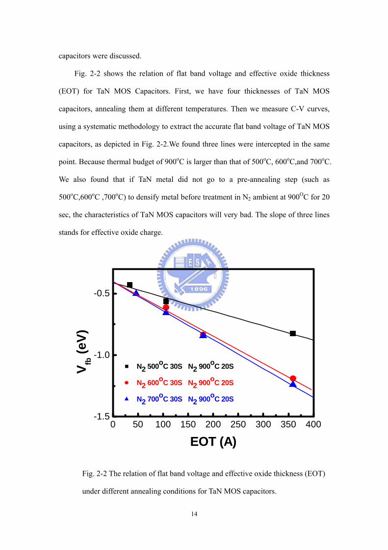

15
Fig 2-3 shows the relation of flat band voltage and effective oxide thickness
(EOT) for MoN MOS Capacitors Like TaN MOS Capacitors we measure C-V curves
using a systematic methodology to extract the accurate flat band voltage of MoN
MOS capacitors as depicted in Fig 2-3 Unlike TaN MOS Capacitors if MoN metal
did not go to a pre-annealing step (such as 500oC and 600oC) to densify metal before
treatment in N2 ambient at 900OC for 20 sec the characteristics of MoN MOS
capacitors will not bad The slope of three lines stands for effective oxide charge
0 50 100 150 200 250 300 350 400 45002
03
04
05
06
07
08 N2 900oC 20S
N2 500oC 30S N2 900oC 20S
N2 600oC 30S N2 900oC 20S
V fb (e
V)
EOT (Α)
Fig 2-3 The relation of flat band voltage and effective oxide thickness (EOT)
under different annealing conditions for MoN MOS capacitors
Fig 2-4 shows work function of TaN metal and current density at Vg = 1V under
different annealing conditions From Fig 2-2 intercept at Y-axis when EOT=0 the
16
value of flat band voltage can extract work function of TaN It shows almost the same
work function value The right Y-axis show the current density at Vg = 1V TaN
metal did not go to a pre-annealing step (such as 500oC 600oC 700oC) to densify
metal before treatment in N2 ambient at 900OC for 20 sec which has the maximum
leakage current density Another TaN metal went to a 700oC pre-annealing step
which has the minimum leakage current density
As 500 600 70043
44
45
46
47
EOT = 338 nmAnneal at 900oC in N2 for 20 sJ measured at Vg = 1 V
Current D
ensity J (Acm
2)
Wor
k fu
nctio
n (e
V)
Pre-annealed Temperature (OC)
1E-6
1E-5
1E-4
Fig 2-4 Work function of TaN metal and current density at Vg = 1V under
different annealing conditions
Fig 2-5 shows work function of MoN metal and current density at Vg = -1V
under different annealing conditions From Fig 2-3 intercept at Y-axis when EOT=0
the value of flat band voltage can extract work function of MoN The metal work
17
function value ranges about 01eV (about 49eV~5eV) The right Y-axis show the
current density at Vg = -1V MoN metal went to a 500oC pre-annealing step to
densify metal before treatment in N2 ambient at 900OC for 20 sec which has the
maximum leakage current density Another MoN metal went to a 600oC
pre-annealing step which has the minimum leakage current density
As 500 600 47
48
49
50
EOT = 338 nmAnneal at 900oC in N2 for 20 sJ measured at Vg = - 1 V
Current D
ensity J (Acm
2)
Wor
k fu
nctio
n (e
V)
Pre-annealed Temperature (OC)
1E-7
1E-6
1E-5
1E-4
As 500 600 47
48
49
50
EOT = 338 nmAnneal at 900oC in N2 for 20 sJ measured at Vg = - 1 V
Current D
ensity J (Acm
2)
Wor
k fu
nctio
n (e
V)
Pre-annealed Temperature (OC)
1E-7
1E-6
1E-5
1E-4
Fig 2-5 Work function of MoN metal and current density at Vg = - 1V under
different annealing conditions
From the above pictures we plot a table to show work function and current
density for different metal and annealing conditions As depicted in Table2-1
18
900E-074622700rarr900TaN
153E-064622600rarr900TaN
254E-054601500rarr900TaN
901E-07497600rarr900MoN
459E-054879500rarr900MoN
999E-07495ASrarr900MoN
Jg atV=1V(Acm-2)
WF(eV)
Condition( OC )
Material
900E-074622700rarr900TaN
153E-064622600rarr900TaN
254E-054601500rarr900TaN
901E-07497600rarr900MoN
459E-054879500rarr900MoN
999E-07495ASrarr900MoN
Jg atV=1V(Acm-2)
WF(eV)
Condition( OC )
Material
Table 2-1 Work function and current density for TaN and MoN metal
2-4 Summary In this chapter we found the work function of TaN was about 46eV It located at
the midgap of energy level so we choose a 700oC pre-annealing step to densify metal
and then treatment at 900OC for 20 sec to fabricate NMOS and PMOS In the other
hand for MoN metal we choose a 600oC pre-annealing step to densify metal and then
treatment at 900OC for 20 sec to fabricate NMOS
19
2-5 Reference
[1] ldquoEffects of High-K Gate Dielectric Materials on Metal and Silicon Gate
Workfunctionsrdquo Yee-Chia Yeo Student Member IEEE Pushkar Ranade
Student Member IEEE Tsu-Jae King Senior Member IEEE and Chenming Hu
Fellow IEEE IEEE ELECTRON DEVICE LETTERS VOL 23 NO 6 JUNE
2002
[2] A Capacitance-Based Methodology for Work Function Extraction of Metals on
High-K Rashmi Jha Jason Gurganos Y H Kim R Choi Jack Lee Member
IEEE and Veena Misra Member IEEE IEEE ELECTRON DEVICE
LETTERS VOL 25 NO 6 JUNE 2004
[3] High work-function metal gate and high-K dielectrics for charge trap flash
memory device applications Sanghun Jeon1 Jeong Hee Han1 Junghoon
Lee1 Cheol Jong Choi2 Sangmoo Choi3 Hyunsang Hwang3 and Chungwoo
Kim Proceedings of ESSDERC Grenoble France 2005
[4] The impact of work-function of metal gate and fixed oxide charge of high-K
blocking dielectric on memory properties ofNAND type charge trap flash
memory devices Sanghun Jeonl Jeong Hee Hani Junghoon Lee1 Jaewoong
Hyun Ju Hyung Kim2 Y S Jeong Hee Soon Chael Soo Doo Chae2 M K
Kim J-W Leel Sangmoo Choi3 Man Jang3 Hyunsang Hwang3 and
Chungwoo Kim1
20
[5] Thermal Instability of Effective Work Function in MetalHigh-K Stack and Its
Material Dependence Moon Sig Joo Byung Jin Cho Senior Member IEEE N
Balasubramanian and Dim-Lee Kwong Senior Member IEEE IEEE
ELECTRON DEVICE LETTERS VOL 25 NO 11 NOVEMBER 2004
21
Chapter 3
Characteristics of High-K CeO2 Nanocrystal
Memory with Different Metal Gates
3-1 Introduction
Charge trapping flash(CTF) memory devices have received considerable attention
due to the detrimental coupling effect among adjacent cells in sub-50nm NAND type
floating gate flash memory devices Nitride based CTF memory devices have several
advantages such as fast programming low power operation high density integration
good reliability characteristics and high compatibility with conventional CMOS
technology However it is difficult to satisfy the NAND specifications of low erase state
Vth of ndash3V from 1V at ndash18V for 2ms and good retention characteristics because the
current through the tunnel dielectric thickness critically affects both properties and the
electron back tunneling (EBT) during erase operation limits the low erase state Vth EBT
is known to a serious concern for meeting specification of NAND devices using
Fowler-Nordheim (FN) program and erase schemes The experimental studies show that
high work-function metal gate and high permittivity (high-K) dielectric play a key role in
eliminating electron back tunneling (EBT) through the blocking dielectric during the
erase operation
In this work in order to reconcile this conflicting behavior we have carried out a
study on the impact of work function of metal gate and high permittivity (high-K)
dielectric on the memory properties of CeO2 based CTF devices Techniques to improve
erase efficiency of CTF memory devices with different metal gates by using n-channel
CeO2 based CTF devices are discussed In the past n-channel flash cells were widely
used in the design of flash memory products However the requirement of high voltage
operation for channel-hot-electron (CHE) programming results in a large power
consumption In order to improve it the p-channel flash cell has been suggested for low
22
voltage and low power applications A more matured p-channel cell using band-to-hand
tunneling induced hot electron injection (BBHE) has later been proposed We
demonstrate reliability enhancement for n-channel and p-channel flash cells
3-2 Experimental Figure 4-1 schematically depicts the process flow of the proposed SONOS flash
memory The fabrication process of the CeO2 nanocrystal memory devices involved was
started with the LOCOS isolation process on p-type and n-type 5-10 Ω cm (100) 150mm
silicon substrates First a 3 nm thick tunnel oxide was thermally grown at 1000OC in
vertical furnace system The trapping layer of CeO2 layer was deposited by dual E-gun
method with CeO2 target After that the samples went through RTA treatment in O2
ambient at 900OC for 1 minute A blocking oxide of about 20 nm thick was then
deposited by high density plasma chemical vapor deposition (HDPCVD) After that the
sample went through RTA treatment in O2 ambient at 900OC for 1 minute For control
samples a 200 nm thick poly-silicon was deposited to serve as the gate electrode by
LPCVD In addition another metal gates 100nm MoN and TaN were deposited by
sputtering method with pure Mo target and pure Ta target in the nitrogen and argon gas
ambient Then gate electrode was patterned For NMOSFET the sourcedrain and gate
were doped by self-aligned P ion implantation at the dosage and energy of 5times1015
ionscm-2 and 25 KeV then the substrate contact was patterned and the sub-contact was
implanted with BF2 at the dosage and energy of 5times1015 ionscm-2 and 40 KeV For
PMOSFET the sourcedrain and gate were doped by self-aligned BF2 ion implantation at
the dosage and energy of 5times1015 ionscm-2 and 25 KeV then the substrate contact was
patterned and the sub-contact was implanted with P at the dosage and energy of 5times1015
ionscm-2 and 40 KeV After these implantations for NMOSFET the dopants were
activated at 950OC for 20 sec For PMOSFET the dopants were activated at 950OC for 10
sec The rest of the subsequent standard CMOS procedures were complete for fabricating
the CeO2 high-k memory devices
23
p-type Si substrate
LOCOSLOCOS
p-type Si substrate
LOCOSLOCOS
p-type Si substrate
LOCOSLOCOSTunneling oxide
p-type Si substrate
LOCOSLOCOSTunneling oxide
p-type Si substrate
LOCOSLOCOSTunneling oxide
CeO2 Trapping layer
p-type Si substrate
LOCOSLOCOSTunneling oxide
CeO2 Trapping layer
O2 RTA 900OC 60secform CeO2 nanocrystal
24
p-type Si substrate
LOCOSLOCOSTunneling oxide
CeO2 nanocrystalBlocking oxide
p-type Si substrate
LOCOSLOCOSTunneling oxide
CeO2 nanocrystalBlocking oxide
p-type Si substrate
LOCOSLOCOSTunneling oxide
CeO2 nanocrystal
Metal Gate
Blocking oxide
p-type Si substrate
LOCOSLOCOSTunneling oxide
CeO2 nanocrystal
Metal Gate
Blocking oxide
25
p-type Si substrate
Tunneling oxideCeO2 nanocrystal
Blocking Oxide
Metal Gate
LOCOSLOCOS
p-type Si substrate
Tunneling oxideCeO2 nanocrystal
Blocking Oxide
Metal Gate
LOCOSLOCOS
p-type Si substrate
Tunneling oxideCeO2 nanocrystal
Blocking Oxide
Metal Gate
LOCOSLOCOS
P31+ Ion implantation
p-type Si substrate
Tunneling oxideCeO2 nanocrystal
Blocking Oxide
Metal Gate
LOCOSLOCOS
p-type Si substrate
Tunneling oxideCeO2 nanocrystal
Blocking Oxide
Metal Gate
LOCOSLOCOSLOCOSLOCOS
P31+ Ion implantation
26
p-type Si substrate
Tunneling oxideCeO2 nanocrystal
Blocking Oxide
Metal Gate
LOCOSLOCOS N+N+
p-type Si substrate
Tunneling oxideCeO2 nanocrystal
Blocking Oxide
Metal Gate
LOCOSLOCOS N+N+
p-type Si substrate
Tunneling oxideCeO2 nanocrystal
Blocking Oxide
Metal Gate
LOCOSLOCOS
metal
N+ N+
SiO2
p-type Si substrate
Tunneling oxideCeO2 nanocrystal
Blocking Oxide
Metal Gate
LOCOSLOCOS
p-type Si substrate
Tunneling oxideCeO2 nanocrystal
Blocking Oxide
Metal Gate
LOCOSLOCOS
p-type Si substrate
Tunneling oxideCeO2 nanocrystal
Blocking Oxide
Metal Gate
LOCOSLOCOS
metal
N+ N+
SiO2
Fig 3-1 The process flow of the metal gate flash memory and the cross-section of
the metal gate flash memory
27
3-3 Results and Discussion In this section the electrical characteristics of metal gate high-k CeO2 nanocrystal
SONOS-type memory were discussed
3-3-1 Id-Vg Curve
0 1 2 3 4 5 6 7 8 910-1310-1210-1110-1010-910-810-710-610-510-410-310-2
Fresh Program state Vg=7V Vd=7V 1msec Erase state Vg=- 3V Vd=8V 1msec
I d (A)
Vg (V)
Fig 3-2 The Id-Vg curves of the MoN metal gate flash memory in the
programmed and erased state
Figure 3-2 shows the Id-Vg curve of the device under program and erase operations
We use channel hot electron injection (CHEI) to program and band to band hot hole to
erase (BTBHH) The program condition is Vg= 7V Vd= 7V with 1 msec stress The erase
condition are Vg= -3V Vd= 8V with 1 msec stress The Vth after programming shifts
28
about 2V from the original fresh state After erasing the Vth shifts leftward 19V So the
memory window is about 2V
-2 -1 0 1 2 3 4 5 6 710-12
10-11
10-10
10-9
10-8
10-7
10-6
10-5
10-4
10-3 Fresh Erase state Vg= - 3V Vd=9V 1msec Program state Vg=7V Vd=7V 1msec
I d (A
)
Vg (V)
Fig 3-3 The Id-Vg curves of the TaN metal gate flash memory in the
programmed and erased state
Figure 3-3 shows the Id-Vg curve of the device under program and erase operations
We use CHEI to program and BTBHH to erase The program condition is Vg= 7V Vd=
7V with 1 msec stress The erase condition are Vg= -3V Vd= 9V with 1 msec stress The
memory window is about 2V
3-3-2 Program and Erase Speed
29
For the high-k CeO2 nanocrystal SONOS-type flash memory with MoN metal gate
the program speed is shown in Fig3-4
10-7 10-6 10-5 10-4 10-3 10-2 10-1 100
0
1
2
3
4
5 Vg=6V Vd=6V Vg=7V Vd=7V Vg=8V Vd=8V Vg=9V Vd=9V
V th s
hift
(V)
Program Time (sec)
Fig 3-4 The program speed curves of high-k CeO2 nanocrystal SONOS-type
flash memory with MoN metal gate
We show four different stress conditions Vg=6VVd=6V Vg=7VVd=7V
Vg=8VVd=8V Vg=9VVd=9V As Fig 3-4 shows the condition Vg=7V Vd=7V 1
msec cause Vth shift about 2V and the condition Vg=8V Vd=8V 01 msec cause Vth
shift over 2V Its memory window is gt 4V At large voltage (such as gt Vg=9V Vd =9)
the program speed is very fast within short time Like the condition Vg=9V Vd =9V 1
usec cause Vth shift 23V
30
10-7 10-6 10-5 10-4 10-3 10-2 10-1 100
0
1
2
3
Initial Vt
Vg=-3V Vd=8V Vg=-4V Vd=8V Vg=-5V Vd=8V
V th
shi
ft (V
)
Erase Time (sec)
Fig 3-5 The erase speed curves of high-k CeO2 nanocrystal SONOS-type flash
memory with MoN metal gate
Figure 3-5 shows the erase speed of the MoN metal gate device For Vg= -3V -4V
and -5V with the same Vd =8V We can see all stress conditions the Vth shift gt 2V in
10msec The final erase state is below the initial state Therefore it shows no electron
back tunneling (EBT) and a little over-erase
For the high-k CeO2 nanocrystal SONOS-type flash memory with TaN metal gate
the program speed is shown in Fig3-6 We show three different stress conditions Vg=5V
Vd=5V Vg=6V Vd=6V Vg=7V Vd=7V As Fig 3-6 shows the condition Vg=7V Vd
=7V 1 msec cause Vth shift about 2V Its memory window is gt 5V
31
10-7 10-6 10-5 10-4 10-3 10-2 10-1 100
0
1
2
3
4
5 Vg=5V Vd=5V Vg=6V Vd=6V Vg=7V Vd=7V
V th
shi
ft (V
)
Program Time (sec)
Fig 3-6 The program speed curves of high-k CeO2 nanocrystal SONOS-type
flash memory with TaN metal gate
Figure 3-7 shows the erase speed of the TaN metal gate device For Vg= -3V -4V
and -5V with the same Vd=9V We can see all stress conditions the Vth shift gt 2V in
10msec And Vt shift of -2V can be achieved with Vg=-4 Vd=9V t lt1ms The final erase
state is below the initial state Because it has no electron back tunneling (EBT) so it
shows over-erase under large erase voltage (such as Vg= -4V Vd=9V and Vg=
-5V Vd=9V)
32
10-7 10-6 10-5 10-4 10-3 10-2 10-1 100-1
0
1
2
3
Initial Vt
Vg=-3V Vd=9V Vg=-4V Vd=9V Vg=-5V Vd=9V
V th
shi
ft (V
)
Erase Time (sec)
Fig 3-7 The erase speed curves of high-k CeO2 nanocrystal SONOS-type flash
memory with TaN metal gate
Figure 3-8 shows the erase speed of the N+-poly and MoN metal gate device To be
clearly understood EBT phenomenon we use F-N tunneling mechanism to erase For
N+-poly gate we can see a little Vth shift under small voltage (Vg=-15V) And EBT
phenomenon occurs when we apply large voltage to it (Vg=-18V) For MoN metal gate
it has no EBT under whether large nor small voltage It shows reasonable erase speed for
MoN metal gate device
33
10-7 10-6 10-5 10-4 10-3 10-2 10-1 1002
3
4
5
6
7
8 N+- poly gate Vg=-15V Vg=-18V
MoN gate Vg=-15V Vg=-18V
V th
shi
ft(V)
Erase Time(sec)
initial Vt
Fig 3-8 The erase speed curves of N+-poly and MoN gate CeO2 nanocrystal
memory with F-N tunneling mechanism
3-3-3 Data Retention Characteristic
Fig 3-9 is the data retention characteristic of MoN metal gate high-k CeO2
nanocrystal SONOS memory measured at 25oC We find the small charge loss with
time The curve shows only 5 charge loss as measure time up to 104 sec and 13
charge loss up to 108 sec at 25oC We infer the small charge loss at room temperature is
from the electron deep trap of high-k CeO2 nanocrystal We prove that sputtering MoN
and TaN metal will not damage the blocking oxide and CeO2 layer so it shows good
retention characteristic
34
100 101 102 103 104 105 106 107 1080
1
2
3
4
5
6
Initial Vt
retention at T=25oC
V th
(V)
Time (sec)
Fig 3-9 Retention characteristic of MoN metal gate high-k CeO2 nanocrystal
SONOS-type flash memory at 25OC
3-3-4 Disturbance Measurement Figure 3-10 shows the gate disturbance measurement of the MoN metal gate device
for three stress conditions Vg=7V Vg= 9V and Vg=11V with Vd =Vs=Vb=0V And
Figure 3-11 shows the gate disturbance measurement of the TaN metal gate device for
three stress conditions Vg=6V Vg= 8V and Vg=10V with Vd =Vs=Vb=0V The applied
gate voltage will attract electrons in the substrate tunneling to the CeO2 layer by FN
tunneling mechanism and result into Vth increase After 1000 sec stress the fresh state
Vth are almost the same It shows almost no gate disturbance after 1000 sec stress
35
100 101 102 103-2
-1
0
1
2
MoN Metal Vg=7V Vg=9V Vg=11V
Er
ase
stat
e V th
shi
ft (V
)
Gate Disturb Time (sec)
Fig 3-10 The gate disturbance characteristics of MoN metal gate device
100 101 102 103-20
-15
-10
-05
00
05
10
15
20
TaN Metal Vg=6V Vg=8V Vg=10V
Eras
e st
ate
V th s
hift
(V)
Gate Disturb Time (sec)
Fig 3-11 The gate disturbance characteristics of TaN metal gate device
36
Figure 3-12 shows the read disturbance measurement of the MoN metal gate device
And Figure 3-13 shows the read disturbance measurement of the TaN metal gate device
The measurement conditions are all fixed Vg=4V with different Vd= 2V 3V and 4V for
1000 sec stress The stress caused the fresh state Vth increase almost 0V It shows almost
no read disturbance after 1000 sec stress
100 101 102 103-2
-1
0
1
2
MoN Metal Vg=4V Vd=2V Vg=4V Vd=3V Vg=4V Vd=4V
Eras
e st
ate
V th s
hift
(V)
Read Disturb Time (sec)
Fig 3-12 The read disturbance characteristics of MoN metal gate device
37
100 101 102 103-2
-1
0
1
2
TaN Metal Vg=4V Vd=2V Vg=4V Vd=3V Vg=4V Vd=4V
Er
ase
stat
e V th
shi
ft (V
)
Read Disturb Time (sec)
Fig 3-13 The gate disturbance characteristics of TaN metal gate device
3-3-5 Physical Characteristics
Fig 3-14 shows the X-ray diffraction (XRD) characteristic of MoN metal gate
device The incident angle ranges from 15 degree to 60 degree We find signal intensity
peak appears at 3285 degree By searching the data base we find the rate between Mo
and N element is 11
Fig 3-15 shows the X-ray diffraction (XRD) characteristic of TaN metal gate device
The incident angle ranges from 15 degree to 60 degree We find signal intensity peak
appears at 33 degree By searching the data base we find the rate between Ta and N
element is 2086
38
20 30 40 50 600
500
1000
1500
2000
XRD Mo1N1
In
tens
ity (c
ps)
2 THETA (deg)
3285
Fig 3-14 The XRD characteristic of MoN metal gate device
28 30 32 34 36 380
5000
10000
15000
20000
XRD Ta2N086
Inte
nsity
(cps
)
2 THETA (deg)
33
Fig 3-15 The XRD characteristic of TaN metal gate device
39
Fig 3-16 The TEM image of MoN metal gate device
Fig 3-16 shows the cross-section-view high resolution tunneling electron
microscopy (HRTEM) of MoN metal gate device From the image the isolation of the
nanocrystals prevents the formation of effective conductive paths between adjacent nodes
The thickness of the tunnel oxide and blocking oxide are about 34nm and 154nm and
the thickness of the MoN metal is about 932nm The nanocrystal size ranges from 75nm
to 98nm
40
3-4 Summary In this chapter we replace conventional poly-Si gate with metal gate MoN TaN We
have shown the electric curves like Id-Vg program speed erase speed and small
disturbance We improve erase efficiency of high-k CeO2 nanocrystal memory with
different metal gates by using p-channel and n-channel devices We also demonstrate the
quality of high-k CeO2 nanocrystal with some good characteristics
41
3-5 Reference [1] Marvin H White Yang (Larry) Yang Ansha Purwar Margaret L Frenchrdquo A Low
Voltage SONOS Nonvolatile Semiconductor Memory Technology rdquo IEEE
transactions on components packaging and manufacturing technologymdashPART A
VOL 20 NO 2 JUNE 1997
[2] Shin-ichi Minami and Yoshiaki Kamigakirdquo A Novel MONOS Nonvolatile Memory
Device Ensuring 10-Year Data Retention after 107 EraseWrite Cycles rdquo IEEE
Transactions on Electron Devices VOL 40 NO 11 NOVEMBER 1993
[3] C C-H Hsu et al Exf Ah SSDM Tsukuba p 1401992
[4] T Ohnakado et al in IEDM Tech Dig p 2791995
[5] Jao-Hsian Shiue et al A study of interface trap generation by Fowler-Nordheim
and Substrate-hot-carrier stresses for 4-nm thick gate oxides in IEEE transactions
on electron devices vol 46 NO8 August 1999
[6] O Takahiro T Hiroshi K Hayashi and M D K Kaisha ldquoNon-volatile
semiconductor memory device capable of high speed programmingerasure US
patent no 5818761rdquo Oct 6 1998
[7] D P Shum et al ldquoA novel band-to-band tunneling induced convergence
mechanism for low current high density Flash EEPROM applicationsrdquo in IEDM
Tech Dig 1994 pp 41ndash44
[8] C-Y Hu et al ldquoSubstrate-current-induced hot electron (SCIHE) injection A new
convergence scheme for Flash memoryrdquo in IEDM Tech Dig 1995 pp 283ndash287
[9] T S Chen K H Wu H Chung and C H Kao ldquoperformance improvement of
SONOS memory by bandgap engineer of charge-trapping layerldquo IEEE Electron
42
Device Lett vol25 no4 pp 205-207 Apr 2002
[10] Marvin H White Yang (Larry) Yang Ansha Purwar Margaret L Frenchrdquo A
Low Voltage SONOS Nonvolatile Semiconductor Memory Technology rdquo IEEE
transactions on components packaging and manufacturing technologymdashPART A
VOL 20 NO 2 JUNE 1997
[11] T Sugizaki M Kohayashi M Ishidao H Minakata M Yamaguchi Y Tamura
Y Sugiyama T Nakanishi and H Tanakardquo Novel Multi-bit SONOS Type Flash
Memory Using a Highk Charge Trapping Layerrdquo Symposium on VLSl Technology
Digest of Technical Papers 2003
[12] Marvin H White Dennis A Adams James R Murray StephenWrazien Yijie
(Sandy) Zhao Yu (Richard) Wang Bilal Khan Wayne Miller Rajiv Mehrotra1rdquo
Characterization of Scaled SONOS EEPROM Memory Devices for Space and
Military Systems rdquo IEEE 2004
[13] G D Wilk R M Wallace J M Anthony rdquoHigh-k gate dielectrics Current status
and materials properties considerations rdquo Applied Physics Review vol89
no10pp5243-5275 Nay 2001
[14] T Ohnakado et al ldquoNovel electron injection method using band-to-band
tunneling induced hot electron (BBHE) for Flash memory with a p-channel cellrdquo
IEDM Tech Dig pp 279ndash282 1995
[15] T Ohnakado et al ldquoNovel self-limiting program scheme utilizing N-channel
select transistors in P-channel DINOR Flash memoryrdquo in IEDM Tech Dig 1996
pp 181ndash184
[16] S J Shen C S Yang Y S Wang and C C-H HsuldquoNovel self-convergent
programming scheme for multilevel P-channel Flash memoryrdquo in IEDM Tech
43
Dig 1997 pp 287ndash290
[17] R-L Lin Y-S Wang and C C-H HsuldquoP-channel Flash memoryrdquo in Proc
NVSMW 1998 pp 27ndash34
[18] T S-D Chang ldquoPMOS memory cell with hot electron injection programming and
tunneling erasing US Patent no 5687118rdquo Nov 11 1997
[19] T S-D Chang ldquoPMOS flash memory cell capable of multi-level threshold
voltage storage US Patent no 5666307rdquo Sept 9 1997
[20] T S-D Changldquonon-volatile electrically erasable memory with PMOS transistor
NAND gate structure US Patent no 5581504rdquo Dec 3 1996
[21] S J Shen C S Yang Y S Wang and C C-H HsuldquoNovel self-convergent
programming scheme for multilevel P-channel Flash memoryrdquo in IEDM Tech
Dig 1997 pp 287ndash290
[22] Frank Ruei-Ling Lin Yen-Sen Wang and Charles Ching-Hsiang Hsu
ldquoMulti-Level P-channel Flash Memoryrdquo pp457-463
[23] Steve S Chung S N Kuo C M Yih and T S Chao ldquoPerformance and
Reliability Evaluations of P-Channel Flash Memories with Different Programming
Schemesrdquo IEDM 97-295
[24] C C-H Hsu et al ldquoA high speed low power p-channel Flash EEPROM using
silicon rich oxide as tunneling dielectricrdquo in Proc Conf Solid State Devices and
Materials 1992 pp 140ndash141
44
Chapter 4
Characteristics of High-K CeO2 Nanocrystal
Memory with Different SourceDrain
Implantations
4-1 Introduction Recently SONOS-type memory has received considerable interest as one of the most
promising candidates to replace the conventional floating-gate flash memory Because as
the tunnel oxide thickness is scaled below 80 Aring the stress-induced leakage current (SILC)
has become such a severe problem that it will be a formidable challenge for floating-gate
devices to meet the ten-year retention requirement However for the SONOS device due
to its discrete charge trapping nature it is more robust to SILC since there is no lateral
charges movement to discharge the whole memory as one single defect is generated in
the tunnel oxide In addition SONOS memory has low operation voltage better
endurance and good compatibility with conventional CMOS process However
achieving fast programming and long retention at the same time remains to be one
challenge for SONOS devices Various approaches have been proposed for improving the
SONOS performance and reliability
In this work we purpose a high performance nonvolatile memory with high-k CeO2
nanocrystal charge trapping layer The serious leakage problem during retention can be
eliminated by utilizing a nanocrystal memory structure The electrons stored on the
nanocrystal directly above the defect chain will be affected since the nanocrystals are
separated from each other within the gate oxide dielectric The tunnel oxide thickness in
the nanocrystal memory device can be reduced to allow faster programming and lower
voltage operation We also use different sourcedrain implantation approaches to achieve
superior memory characteristics
45
4-2 Experimental Figure 4-1 schematically depicts the process flow of the proposed SONOS flash
memory
p-type Si substrate
LOCOSLOCOS
p-type Si substrate
LOCOSLOCOS
p-type Si substrate
LOCOSLOCOSTunneling oxide
CeO2 nanocrystal
Poly-Si Gate
Blocking oxide
p-type Si substrate
LOCOSLOCOSTunneling oxide
CeO2 nanocrystal
Poly-Si Gate
Blocking oxide
46
p-type Si substrate
Tunneling oxideCeO2 nanocrystal
Blocking Oxide
Poly-Si Gate
LOCOSLOCOS N+N+
p-type Si substrate
Tunneling oxideCeO2 nanocrystal
Blocking Oxide
Poly-Si Gate
LOCOSLOCOS N+N+
p-type Si substrate
Tunneling oxideCeO2 nanocrystal
Blocking Oxide
Poly-Si Gate
LOCOSLOCOS
metal
N+ N+
SiO2
p-type Si substrate
Tunneling oxideCeO2 nanocrystal
Blocking Oxide
Poly-Si Gate
LOCOSLOCOS
p-type Si substrate
Tunneling oxideCeO2 nanocrystal
Blocking Oxide
Poly-Si Gate
LOCOSLOCOS
p-type Si substrate
Tunneling oxideCeO2 nanocrystal
Blocking Oxide
Poly-Si Gate
LOCOSLOCOS
metal
N+ N+
SiO2
47
Fig 4-1 The process flow of the flash memory and the cross-section of the flash
memory (control samples)
The fabrication process of the CeO2 nanocrystal memory devices involved was
started with the LOCOS isolation process on p-type 5-10 Ω cm (100) 150mm silicon
substrates First a 2 nm thick tunnel oxide was thermally grown at 1000OC in vertical
furnace system The trapping layer of CeO2 layer was deposited by dual E-gun method
with CeO2 target After that the samples went through RTA treatment in O2 ambient at
900OC for 1 minute A blocking oxide of about 20 nm thick was then deposited by high
density plasma chemical vapor deposition (HDPCVD) After that the sample went
through RTA treatment in O2 ambient at 900OC for 1 minute Then a 200 nm thick
poly-silicon was deposited to serve as the gate electrode by LPCVD Then gate electrode
was patterned and the sourcedrain and gate were doped by self-aligned P ion
implantation at the dosage and energy of 5times1015 ionscm-2 and 25 KeV then the substrate
contact was patterned and the sub-contact was implanted with BF2 at the dosage and
energy of 5times1015 ionscm-2 and 40 KeV After these implantations the dopants were
activated at 950OC for 20 sec The rest of the subsequent standard CMOS procedures
were complete for fabricating the CeO2 high-k memory devices The above are control
samples
48
p-type Si substrate
Tunneling oxideCeO2 nanocrystal
Blocking Oxide
Poly-Si Gate
LOCOSLOCOS
BF2 ion implantation
p-type Si substrate
Tunneling oxideCeO2 nanocrystal
Blocking Oxide
Poly-Si Gate
LOCOSLOCOS
p-type Si substrate
Tunneling oxideCeO2 nanocrystal
Blocking Oxide
Poly-Si Gate
LOCOSLOCOS
BF2 ion implantation
p-type Si substrate
Tunneling oxideCeO2 nanocrystal
Blocking Oxide
Poly-Si Gate
LOCOSLOCOS
P31+ ion implantation
p-type Si substrate
Tunneling oxideCeO2 nanocrystal
Blocking Oxide
Poly-Si Gate
LOCOSLOCOSLOCOSLOCOS
P31+ ion implantation
49
p-type Si substrate
Tunneling oxideCeO2 nanocrystal
Blocking Oxide
Poly-Si Gate
LOCOSLOCOS N+N+ P+
p-type Si substrate
Tunneling oxideCeO2 nanocrystal
Blocking Oxide
Poly-Si Gate
LOCOSLOCOS N+N+ P+
p-type Si substrate
Tunneling oxideCeO2 nanocrystal
Blocking Oxide
Poly-Si Gate
LOCOSLOCOS
metal
N+ N+P+
SiO2
p-type Si substrate
Tunneling oxideCeO2 nanocrystal
Blocking Oxide
Poly-Si Gate
LOCOSLOCOS
p-type Si substrate
Tunneling oxideCeO2 nanocrystal
Blocking Oxide
Poly-Si Gate
LOCOSLOCOS
metal
N+ N+P+
SiO2
Fig 4-2 The process flow and the cross-section of the asymmetry sourcedrain
50
flash memory (asymmetry SD)
Figure 4-2 schematically depicts the process flow of the asymmetry sourcedrain
SONOS flash memory We changed the sourcedrain implantation with BF2 ion
implantation at the dosage and energy of 5times1013 ionscm-2 and 25 KeV (twist angle 72
degree tilt angle 30degree) then doped by P ion implantation at the dosage and energy
of 5times1015 ionscm-2 and 25 KeV (twist angle 0 degree tilt angle 0 degree) Then the
substrate contact was patterned and the sub-contact was implanted with BF2 at the dosage
and energy of 5times1015 ionscm-2 and 40 KeV After these implantations the dopants were
activated at 950OC for 20 sec The rest of the subsequent standard CMOS procedures
were complete for fabricating the CeO2 high-k memory devices
4-3 Results and Discussion In this section the electrical characteristics of high-k CeO2 nanocrystal SONOS-type
memory were discussed
4-3-1 Id-Vg Curve Figure 4-3 shows the Id-Vg curves of the device under program and erase
operations
51
2 3 4 5 6 7 8 9 101E-12
1E-11
1E-10
1E-9
1E-8
1E-7
1E-6
1E-5
1E-4
1E-3 Fresh Program state Vg=7V Vd=7V 10msec Erase state Vg=-4V Vd=8V 10msec
I d (A
)
Vg (V)
Fig 4-3 The Id-Vg curves of the high-k CeO2 nanocrystal SONOS-type flash
memory in the programmed and erase state
We use channel hot electron injection (CHEI) to program and band to band hot hole
to erase (BTBHH) The program condition is Vg= 7V Vd= 7V with 10 msec stress The
erase condition are Vg= -4V Vd= 8V with 10 msec stress The Vth after programming
shifts about 3V from the original fresh state After erasing the Vth shifts leftward about
27V So the memory window is about 3V We think the Vth shift rightward is due to
electron trapping in the high-k CeO2 nanocrystal layer The band offset is the reason why
trapping occurred During programming the electrons in the substrate gain energy from
the applied voltage Vg and Vd If the energy is enough to cross the energy barrier the hot
electrons will inject to the high-k CeO2 nanocrystal charge trapping layer and be trapped
This causes the Vth change When erasing we apply a negative gate voltage and positive
52
drain voltage to generate hot hole in the substrate If the hot hole in the substrate achieves
enough energy to cross the energy barrier it can reach the high-k CeO2 nanocrystal
charge trapping layer and cause the Id-Vg curve shift toward left
0 1 2 3 4 5 6 7 810-12
10-11
10-10
10-9
10-8
10-7
10-6
10-5
10-4
10-3
Fresh Program state Vg=7V Vd=7V 1msec Erase state Vg=-4V Vd=8V 10msec
I d (A
)
Vg (V)
Fig 4-4 The Id-Vg curves of the asymmetry sourcedrain high-k CeO2
nanocrystal SONOS-type flash memory
Figure 4-4 shows the Id-Vg curves of the device under program and erase operations
We use channel hot electron injection (CHEI) to program and band to band hot hole to
erase (BTBHH) The program condition is Vg= 7V Vd= 7V with 1 msec stress The erase
condition are Vg= -4V Vd= 8V with 10 msec stress The Vth after programming shifts
about 23V from the original fresh state After erasing the Vth shifts leftward about 23V
So the memory window is about 23V
4-3-2 Program and Erase Speed
53
For the control samples the program speed is shown in Fig 4-5
10-7 10-6 10-5 10-4 10-3 10-2 10-1 100
0
1
2
3
4
5
6 Vg=6V Vd=6V Vg=7V Vd=7V Vg=8V Vd=8V Vg=9V Vd=9V
V th s
hift
(V)
Program Time(sec)
Fig 4-5 The program speed curve of high-k CeO2 nanocrystal SONOS-type flash
memory
We show four different stress conditions Vg=6VVd=6V Vg=7VVd=7V
Vg=8VVd=8V Vg=9VVd=9V As Fig 4-5 shows the condition Vg=7V Vd=7V 1
msec cause Vth shift 2V and the condition Vg=8V Vd=8V 01 msec cause Vth shift 2V
With the Vg and Vd increasing the Vth shift also increases and the program speed is
faster memory window is gt 5V This is because as the gate voltage become more
positive for programming more hot electrons are generated So more and more hot
electrons can be trapped in the charge trapping layer Hence the Vth shift increases as
gate voltage and drain voltage increases
54
1E-7 1E-6 1E-5 1E-4 1E-3 001 01 10
1
2
3
4
5
6
7Vg Vs
Vg=6V Vd=6V Vg=7V Vd=7V Vg=8V Vd=8V
Vg Vd Vg=6V Vd=6V Vg=7V Vd=7V Vg=8V Vd=8V
V th s
hift(
V)
Program Time(sec)
Fig 4-6 The program speed curves of asymmetry sourcedrain high-k CeO2
nanocrystal SONOS-type flash memory
55
Fig 4-7 The band diagram of P+-N junction at reverse bias
Figure 4-6 shows the program speed of the asymmetry sourcedrain device First
define n-type only region as source define n-type and p-type region as drain We show
three different stress conditions Vg=6VVd=6V Vg=7VVd=7V Vg=8VVd=8V
compare with Vg=6VVs=6V Vg=7VVs=7V Vg=8VVs=8V As Fig 4-5 shows both
the condition Vg=7V Vd=7V and the condition Vg=7V Vs=7V 1 msec cause Vth shift
gt 2V With the Vg and VdVs increasing the Vth shift also increases and the program
speed is faster memory window is gt 6V Hence the Vth shift increases as gate voltage
and drain voltage source voltage increases When the drain voltage applies to the drain
region the p+-n junction is at reverse-biased condition so band bending becomes more
serious and then occurs zener breakdown as depicted in Fig 4-7 Therefore near drain
region more and more electron hole pairs generate so more and more hot electrons can
be trapped in the charge trapping layer In Fig 4-8 we prove high drain current under the
same drain and gate voltage the asymmetry sourcedrain device than the normal
sourcedrain device It means more and more electron hole pairs generate
Ec Ef Ev
P+ N
Vd
56
0 1 2 3 400
20x10-5
40x10-5
60x10-5
IdVd Vg-Vt=2V Vg-Vt=4V Vg-Vt=6V
IsVs Vg-Vt=2V Vg-Vt=4V Vg-Vt=6V
I d I s (V
)
Vd Vs (V)
Fig 4-8 The Id-Vd Is-Vs curves of the asymmetry sourcedrain high-k CeO2
nanocrystal SONOS-type flash memory
57
10-7 10-6 10-5 10-4 10-3 10-2 10-1 1000
1
2
3
4
5
6
7control
Vg=6V Vd=6V Vg=7V Vd=7V Vg=8V Vd=8V
changed Vg=6V Vd=6V Vg=7V Vd=7V Vg=8V Vd=8V
V th
shi
ft(V)
Program Time(sec)
Fig 4-9 The program speed curve of normal and asymmetry sourcedrain high-k
CeO2 nanocrystal SONOS-type flash memory
Figure 4-9 shows the program speed of the control device and asymmetry
sourcedrain device We show three different stress conditions Vg=6VVd=6V
Vg=7VVd=7V Vg=8VVd=8V With the Vg and VdVs increasing the Vth shift also
increases and the program speed is faster memory window is gt 6V Hence the Vth shift
increases as gate voltage and drain voltage increases Compared with control samples the
band bending of the p+-n junction at reverse-biased condition is more serious and occurs
zener breakdown Therefore more electron hole pairs generate more hot electrons can be
trapped in the charge trapping layer So the program speed of the asymmetry
sourcedrain device is faster than control device We prove this comment with Fig 4-10
58
0 1 2 3 400
20x10-5
40x10-5
60x10-5
control Vg-Vt=2V Vg-Vt=4V Vg-Vt=6V
changed Vg-Vt=2V Vg-Vt=4V Vg-Vt=6V
I d (V
)
Vd (V)
Fig 4-10 The Id-Vd curves of normal and asymmetry sourcedrain high-k CeO2
nanocrystal SONOS-type flash memory
Figure 4-11 shows the normalized erase speed of the device For Vg= -3V -4V and
-5V with the same Vd=8V We can see as the gate voltage becomes more negative the
Vth shift a little more and all stress conditions the Vth shift gt 25V in 10msec For Vd=
6V 7V and 8V with the same Vg= -4V We can see as the drain voltage becomes more
positive the Vth shift more Hence the Vth shift increases as gate voltage increases or
drain voltage increases Drain voltage influnces the erase speed is large than gate voltage
59
10-7 10-6 10-5 10-4 10-3 10-2 10-1 100-4
-3
-2
-1
0
Vg=-3V Vd=8V Vg=-4V Vd=8V Vg=-5V Vd=8V Vg=-4V Vd=6V Vg=-4V Vd=7V
V th s
hift(
V)
Erase Time(sec)
Fig 4-11 The erase speed curve of high-k CeO2 nanocrystal SONOS-type flash
memory
60
10-7 10-6 10-5 10-4 10-3 10-2 10-1 100
-4
-3
-2
-1
0
Vg Vs Vg=-4V Vd=6V Vg=-4V Vd=7V Vg=-4V Vd=8V
Vg Vd Vg=-4V Vd=6V Vg=-4V Vd=7V Vg=-4V Vd=8V
V th
shi
ft(V)
Erase Time(sec)
Fig 4-12 The erase speed curve of asymmetry sourcedrain high-k CeO2
nanocrystal SONOS-type flash memory
Figure 4-12 shows the normalized erase speed of the asymmetry sourcedrain device
For Vd= 6V 7V and 8V with the same Vg= -4V At low voltage (6V) the band
bending of high-dose P+-N junction at reversed bias is more serious than that of low-dose
P-N junction at reversed bias So more and more electron hole pairs generate near drain
region than that near source region The erase speed of condition Vg= -4V Vd= 6V is
more faster than condition Vg= -4V Vs= 6V At high voltage the band bending of
high-dose P+-N junction and low-dose P-N junction at reversed bias are all serious
Therefore the erase speeds of them are almost the same
Figure 4-13 shows the erase speed of the control device and asymmetry
sourcedrain device For Vd= 6V 7V and 8V with the same Vg= -4V This is also
61
because the band bending of high-dose P+-N junction (asymmetry sourcedrain) at
reversed bias is more serious than that of low-dose P-N junction (control samples) at
reversed bias Therefore the erase speed of the asymmetry sourcedrain device is faster
than control samples
10-7 10-6 10-5 10-4 10-3 10-2 10-1 100
-4
-3
-2
-1
0
control Vg=-4V Vd=6V Vg=-4V Vd=7V Vg=-4V Vd=8V
changed Vg=-4V Vd=6V Vg=-4V Vd=7V Vg=-4V Vd=8V
V th s
hift
(V)
Erase Time(sec)
Fig 4-13 The erase speed curves of normal and asymmetry sourcedrain high-k
CeO2 nanocrystal SONOS-type flash memory
62
4-3-3 Data Retention Characteristic Fig 4-14 is the data retention characteristic of high-k CeO2 nanocrystal SONOS
memory measured at 25oC We find the small charge loss with time The curve shows
only 85 charge loss as measure time up to 104 sec and 16 charge loss up to 108 sec at
25oC We infer the small charge loss at room temperature is from the electron deep trap of
high-k CeO2 nanocrystal charge trapping layer mentioned above
100 101 102 103 104 105 106 107 10800
05
10
15
20
25
30
35
40
Initial Vt
retention at T=25oC
V th (V
)
Time (sec)
Fig 4-14 Retention characteristic of the high-k CeO2 nanocrystal SONOS-type
flash memory at 25OC
63
4-3-4 Disturbance Measurement Figure 4-15 shows drain disturbance measurement of the normal and asymmetry
sourcedrain high-k CeO2 nanocrystal device We applied two stress conditions Vd =6V
and Vd=8V with Vg=Vs=Vb=0V to the device From the Fig 4-12 we can see little Vth
loss after 1000 sec stress for normal device the programmed state Vth loss is 015V at
Vd=6V and 023V for Vd=8V for the asymmetry sourcedrain device
100 101 102 103-03
-02
-01
00
01
02
03
Prog
ram
stat
e V
th sh
ift (V
)
Drain Disturb Time (sec)
controlVd=6V Vd=8V
changed Vd=6V Vd=8V
Fig 4-15 Drain disturbance characteristics of normal and asymmetry
sourcedrain high-k CeO2 nanocrystal SONOS-type flash memory
64
4-4 Summary In this chapter we propose a new sourcedrain implantation method for high-k CeO2
nanocrystal SONOS memory We have shown the electric curves like Id-Vg
programerase speed charge retention and drain disturbance We demonstrate the quality
of high-k CeO2 nanocrystal with some good characteristics in terms of large memory
window long charge retention time due to deep trap level in the CeO2 layer and small
drain disturbance
65
4-5 Reference [1] H Aozasa I Fujiwara A Nakamura and Y Komatsu ldquoAnalysis of Carrier Traps
in Si3N4 in OxideNitrideOxide for Metal OxideNitrideOxide Silicon Nonvolatile
Memoryrdquo Japanese Journal of Applied Physics Vol38 part 1 No 3A
pp1441-1447 1999
[2] Y Yang and M H White ldquoCharge retention of scaled SONOS nonvolatile
memory devices at elevated temperaturesrdquo Solid State Electronics Vol 44
pp949-958 2000
[3] YN Tan WK Chim BJ Cho and WK Choi ldquoOver-erase phenomenon in
SONOS-type flash memory and its minimization using a hafnium oxide charge
storage layerrdquo IEEE Trans Electron Devices vol 51 pp 1143-1147 July 2004
[4] G D Wilk R M Wallace and J M Anthony ldquoHigh-k gate dielectrics Current
status and materials properties considerationsrdquo Journal of Applied Physics Vol 89
pp 5243-5275 2001
[5] W Zhu TP Ma T Tamagawa Y Di J Kim R Carruthers M Gibson and T
Furukawa ldquoHfO2 and HfAlO for CMOS Thermal stability and current transportrdquo
in IEDM Tech Dig pp 463-466 2001
[6] S Ventkataraj O Kappertz C Liesch R Detemple R Jayavel M Wutting
Vacuum 75 7 (2004)
[7] W Zhao B K Tay G Q Yu S P Lau J Phys ndashCondens Mat 15 7707 (2003)
[8] A J Moulson and J M Herbert Electroceramics Wiley NJ (2003)
[9] W Zhu TP Ma T Tamagawa Y Di J Kim R Carruthers M Gibson T
Furukawa IEDM 463 (2001)
66
[10] M Balog M Schieber M Michman and S Patai Thin Solid films 47 190
(1997)
[11] M Balog and M Schieber J Electrochem Soc 1261203 (1979)
[12] WJ Tsai NK Zous CJ Liu CH Chen Tahui Wang Sam Pan and C-Y Lu
IEDM 719 (2001)
[13] Y-H Shih H-T Lue K-Y Hsieh Rich Liu and C-Y Lu IEDM 881 (2004)
[14] C T Swift G L Chindalore K Harber T S Harp A Hoefler C M Hong P
A Ingersoll C B Li E J Prinz and J A Yater IEDM 927 (2002)
67
Chapter 5
Conclusions The thesis of ldquoThe Study of High-K CeO2 Nanocrystal Flash Memory with
Different Metal Gates and SD Implantationsrdquo was proposed The results of each
chapter are summarized as below
In chapter 2 we discuss the dependence of metal gate work functions on the
different annealing temperatures We found a systematic methodology to extract the
accurate work function of metal gates We found the work function of TaN was about
46eV It located at the midgap of energy level so we choose a 700oC pre-annealing
step to densify metal and then treatment at 900OC for 20 sec to fabricate NMOS In
the other hand for MoN metal we choose a 600oC pre-annealing step to densify metal
and then treatment at 900OC for 20 sec to fabricate NMOS
In chapter 3 we replace conventional poly-Si gate with MoN and TaN metal
gates We have shown the electric curves like Id-Vg program speed erase speed and
disturbances We improve erase efficiency of high-k CeO2 nanocrystal memory with
different metal gates by using n-channel devices We also demonstrate the quality of
high-k CeO2 nanocrystal with some good characteristic in terms of large memory
window long charge retention time and small gate disturbance and read disturbance
In chapter 4 we propose a new sourcedrain implantation method to high-k CeO2
nanocrystal SONOS memory We have shown the electric curves like Id-Vg
programerase speedcharge retention and drain disturbance We demonstrate the
68
quality of high-k CeO2 nanocrystal with some good characteristics in terms of large
memory window long charge retention time due to deep trap level in the CeO2
nanocrystal and small drain disturbance
簡歷
姓 名 余 明 爵
性 別 男
出生日期 中華民國七十二年五月十一日
籍 貫 台灣省 桃園縣桃園市
地 址 桃園縣八德市廣德里 16 鄰順昌街 72 巷 1 號
學 歷 國立清華大學 工程與系統科學系
(民國 94 年 6 月)
國立交通大學 電子研究所固態組 碩士班
(民國 96 年 6 月)
論文題目 應用不同金屬閘極和源極汲極離子佈植於二氧化鈰
奈米微晶粒之 SONOS 記憶體研究
The Study of High-K CeO2 Nanocrystal Flash Memory
with Different Metal Gates and SourceDrain
Implantations
電子郵件u902131alumninthuedutw

20
[5] Thermal Instability of Effective Work Function in MetalHigh-K Stack and Its
Material Dependence Moon Sig Joo Byung Jin Cho Senior Member IEEE N
Balasubramanian and Dim-Lee Kwong Senior Member IEEE IEEE
ELECTRON DEVICE LETTERS VOL 25 NO 11 NOVEMBER 2004
21
Chapter 3
Characteristics of High-K CeO2 Nanocrystal
Memory with Different Metal Gates
3-1 Introduction
Charge trapping flash(CTF) memory devices have received considerable attention
due to the detrimental coupling effect among adjacent cells in sub-50nm NAND type
floating gate flash memory devices Nitride based CTF memory devices have several
advantages such as fast programming low power operation high density integration
good reliability characteristics and high compatibility with conventional CMOS
technology However it is difficult to satisfy the NAND specifications of low erase state
Vth of ndash3V from 1V at ndash18V for 2ms and good retention characteristics because the
current through the tunnel dielectric thickness critically affects both properties and the
electron back tunneling (EBT) during erase operation limits the low erase state Vth EBT
is known to a serious concern for meeting specification of NAND devices using
Fowler-Nordheim (FN) program and erase schemes The experimental studies show that
high work-function metal gate and high permittivity (high-K) dielectric play a key role in
eliminating electron back tunneling (EBT) through the blocking dielectric during the
erase operation
In this work in order to reconcile this conflicting behavior we have carried out a
study on the impact of work function of metal gate and high permittivity (high-K)
dielectric on the memory properties of CeO2 based CTF devices Techniques to improve
erase efficiency of CTF memory devices with different metal gates by using n-channel
CeO2 based CTF devices are discussed In the past n-channel flash cells were widely
used in the design of flash memory products However the requirement of high voltage
operation for channel-hot-electron (CHE) programming results in a large power
consumption In order to improve it the p-channel flash cell has been suggested for low
22
voltage and low power applications A more matured p-channel cell using band-to-hand
tunneling induced hot electron injection (BBHE) has later been proposed We
demonstrate reliability enhancement for n-channel and p-channel flash cells
3-2 Experimental Figure 4-1 schematically depicts the process flow of the proposed SONOS flash
memory The fabrication process of the CeO2 nanocrystal memory devices involved was
started with the LOCOS isolation process on p-type and n-type 5-10 Ω cm (100) 150mm
silicon substrates First a 3 nm thick tunnel oxide was thermally grown at 1000OC in
vertical furnace system The trapping layer of CeO2 layer was deposited by dual E-gun
method with CeO2 target After that the samples went through RTA treatment in O2
ambient at 900OC for 1 minute A blocking oxide of about 20 nm thick was then
deposited by high density plasma chemical vapor deposition (HDPCVD) After that the
sample went through RTA treatment in O2 ambient at 900OC for 1 minute For control
samples a 200 nm thick poly-silicon was deposited to serve as the gate electrode by
LPCVD In addition another metal gates 100nm MoN and TaN were deposited by
sputtering method with pure Mo target and pure Ta target in the nitrogen and argon gas
ambient Then gate electrode was patterned For NMOSFET the sourcedrain and gate
were doped by self-aligned P ion implantation at the dosage and energy of 5times1015
ionscm-2 and 25 KeV then the substrate contact was patterned and the sub-contact was
implanted with BF2 at the dosage and energy of 5times1015 ionscm-2 and 40 KeV For
PMOSFET the sourcedrain and gate were doped by self-aligned BF2 ion implantation at
the dosage and energy of 5times1015 ionscm-2 and 25 KeV then the substrate contact was
patterned and the sub-contact was implanted with P at the dosage and energy of 5times1015
ionscm-2 and 40 KeV After these implantations for NMOSFET the dopants were
activated at 950OC for 20 sec For PMOSFET the dopants were activated at 950OC for 10
sec The rest of the subsequent standard CMOS procedures were complete for fabricating
the CeO2 high-k memory devices
23
p-type Si substrate
LOCOSLOCOS
p-type Si substrate
LOCOSLOCOS
p-type Si substrate
LOCOSLOCOSTunneling oxide
p-type Si substrate
LOCOSLOCOSTunneling oxide
p-type Si substrate
LOCOSLOCOSTunneling oxide
CeO2 Trapping layer
p-type Si substrate
LOCOSLOCOSTunneling oxide
CeO2 Trapping layer
O2 RTA 900OC 60secform CeO2 nanocrystal
24
p-type Si substrate
LOCOSLOCOSTunneling oxide
CeO2 nanocrystalBlocking oxide
p-type Si substrate
LOCOSLOCOSTunneling oxide
CeO2 nanocrystalBlocking oxide
p-type Si substrate
LOCOSLOCOSTunneling oxide
CeO2 nanocrystal
Metal Gate
Blocking oxide
p-type Si substrate
LOCOSLOCOSTunneling oxide
CeO2 nanocrystal
Metal Gate
Blocking oxide
25
p-type Si substrate
Tunneling oxideCeO2 nanocrystal
Blocking Oxide
Metal Gate
LOCOSLOCOS
p-type Si substrate
Tunneling oxideCeO2 nanocrystal
Blocking Oxide
Metal Gate
LOCOSLOCOS
p-type Si substrate
Tunneling oxideCeO2 nanocrystal
Blocking Oxide
Metal Gate
LOCOSLOCOS
P31+ Ion implantation
p-type Si substrate
Tunneling oxideCeO2 nanocrystal
Blocking Oxide
Metal Gate
LOCOSLOCOS
p-type Si substrate
Tunneling oxideCeO2 nanocrystal
Blocking Oxide
Metal Gate
LOCOSLOCOSLOCOSLOCOS
P31+ Ion implantation
26
p-type Si substrate
Tunneling oxideCeO2 nanocrystal
Blocking Oxide
Metal Gate
LOCOSLOCOS N+N+
p-type Si substrate
Tunneling oxideCeO2 nanocrystal
Blocking Oxide
Metal Gate
LOCOSLOCOS N+N+
p-type Si substrate
Tunneling oxideCeO2 nanocrystal
Blocking Oxide
Metal Gate
LOCOSLOCOS
metal
N+ N+
SiO2
p-type Si substrate
Tunneling oxideCeO2 nanocrystal
Blocking Oxide
Metal Gate
LOCOSLOCOS
p-type Si substrate
Tunneling oxideCeO2 nanocrystal
Blocking Oxide
Metal Gate
LOCOSLOCOS
p-type Si substrate
Tunneling oxideCeO2 nanocrystal
Blocking Oxide
Metal Gate
LOCOSLOCOS
metal
N+ N+
SiO2
Fig 3-1 The process flow of the metal gate flash memory and the cross-section of
the metal gate flash memory
27
3-3 Results and Discussion In this section the electrical characteristics of metal gate high-k CeO2 nanocrystal
SONOS-type memory were discussed
3-3-1 Id-Vg Curve
0 1 2 3 4 5 6 7 8 910-1310-1210-1110-1010-910-810-710-610-510-410-310-2
Fresh Program state Vg=7V Vd=7V 1msec Erase state Vg=- 3V Vd=8V 1msec
I d (A)
Vg (V)
Fig 3-2 The Id-Vg curves of the MoN metal gate flash memory in the
programmed and erased state
Figure 3-2 shows the Id-Vg curve of the device under program and erase operations
We use channel hot electron injection (CHEI) to program and band to band hot hole to
erase (BTBHH) The program condition is Vg= 7V Vd= 7V with 1 msec stress The erase
condition are Vg= -3V Vd= 8V with 1 msec stress The Vth after programming shifts
28
about 2V from the original fresh state After erasing the Vth shifts leftward 19V So the
memory window is about 2V
-2 -1 0 1 2 3 4 5 6 710-12
10-11
10-10
10-9
10-8
10-7
10-6
10-5
10-4
10-3 Fresh Erase state Vg= - 3V Vd=9V 1msec Program state Vg=7V Vd=7V 1msec
I d (A
)
Vg (V)
Fig 3-3 The Id-Vg curves of the TaN metal gate flash memory in the
programmed and erased state
Figure 3-3 shows the Id-Vg curve of the device under program and erase operations
We use CHEI to program and BTBHH to erase The program condition is Vg= 7V Vd=
7V with 1 msec stress The erase condition are Vg= -3V Vd= 9V with 1 msec stress The
memory window is about 2V
3-3-2 Program and Erase Speed
29
For the high-k CeO2 nanocrystal SONOS-type flash memory with MoN metal gate
the program speed is shown in Fig3-4
10-7 10-6 10-5 10-4 10-3 10-2 10-1 100
0
1
2
3
4
5 Vg=6V Vd=6V Vg=7V Vd=7V Vg=8V Vd=8V Vg=9V Vd=9V
V th s
hift
(V)
Program Time (sec)
Fig 3-4 The program speed curves of high-k CeO2 nanocrystal SONOS-type
flash memory with MoN metal gate
We show four different stress conditions Vg=6VVd=6V Vg=7VVd=7V
Vg=8VVd=8V Vg=9VVd=9V As Fig 3-4 shows the condition Vg=7V Vd=7V 1
msec cause Vth shift about 2V and the condition Vg=8V Vd=8V 01 msec cause Vth
shift over 2V Its memory window is gt 4V At large voltage (such as gt Vg=9V Vd =9)
the program speed is very fast within short time Like the condition Vg=9V Vd =9V 1
usec cause Vth shift 23V
30
10-7 10-6 10-5 10-4 10-3 10-2 10-1 100
0
1
2
3
Initial Vt
Vg=-3V Vd=8V Vg=-4V Vd=8V Vg=-5V Vd=8V
V th
shi
ft (V
)
Erase Time (sec)
Fig 3-5 The erase speed curves of high-k CeO2 nanocrystal SONOS-type flash
memory with MoN metal gate
Figure 3-5 shows the erase speed of the MoN metal gate device For Vg= -3V -4V
and -5V with the same Vd =8V We can see all stress conditions the Vth shift gt 2V in
10msec The final erase state is below the initial state Therefore it shows no electron
back tunneling (EBT) and a little over-erase
For the high-k CeO2 nanocrystal SONOS-type flash memory with TaN metal gate
the program speed is shown in Fig3-6 We show three different stress conditions Vg=5V
Vd=5V Vg=6V Vd=6V Vg=7V Vd=7V As Fig 3-6 shows the condition Vg=7V Vd
=7V 1 msec cause Vth shift about 2V Its memory window is gt 5V
31
10-7 10-6 10-5 10-4 10-3 10-2 10-1 100
0
1
2
3
4
5 Vg=5V Vd=5V Vg=6V Vd=6V Vg=7V Vd=7V
V th
shi
ft (V
)
Program Time (sec)
Fig 3-6 The program speed curves of high-k CeO2 nanocrystal SONOS-type
flash memory with TaN metal gate
Figure 3-7 shows the erase speed of the TaN metal gate device For Vg= -3V -4V
and -5V with the same Vd=9V We can see all stress conditions the Vth shift gt 2V in
10msec And Vt shift of -2V can be achieved with Vg=-4 Vd=9V t lt1ms The final erase
state is below the initial state Because it has no electron back tunneling (EBT) so it
shows over-erase under large erase voltage (such as Vg= -4V Vd=9V and Vg=
-5V Vd=9V)
32
10-7 10-6 10-5 10-4 10-3 10-2 10-1 100-1
0
1
2
3
Initial Vt
Vg=-3V Vd=9V Vg=-4V Vd=9V Vg=-5V Vd=9V
V th
shi
ft (V
)
Erase Time (sec)
Fig 3-7 The erase speed curves of high-k CeO2 nanocrystal SONOS-type flash
memory with TaN metal gate
Figure 3-8 shows the erase speed of the N+-poly and MoN metal gate device To be
clearly understood EBT phenomenon we use F-N tunneling mechanism to erase For
N+-poly gate we can see a little Vth shift under small voltage (Vg=-15V) And EBT
phenomenon occurs when we apply large voltage to it (Vg=-18V) For MoN metal gate
it has no EBT under whether large nor small voltage It shows reasonable erase speed for
MoN metal gate device
33
10-7 10-6 10-5 10-4 10-3 10-2 10-1 1002
3
4
5
6
7
8 N+- poly gate Vg=-15V Vg=-18V
MoN gate Vg=-15V Vg=-18V
V th
shi
ft(V)
Erase Time(sec)
initial Vt
Fig 3-8 The erase speed curves of N+-poly and MoN gate CeO2 nanocrystal
memory with F-N tunneling mechanism
3-3-3 Data Retention Characteristic
Fig 3-9 is the data retention characteristic of MoN metal gate high-k CeO2
nanocrystal SONOS memory measured at 25oC We find the small charge loss with
time The curve shows only 5 charge loss as measure time up to 104 sec and 13
charge loss up to 108 sec at 25oC We infer the small charge loss at room temperature is
from the electron deep trap of high-k CeO2 nanocrystal We prove that sputtering MoN
and TaN metal will not damage the blocking oxide and CeO2 layer so it shows good
retention characteristic
34
100 101 102 103 104 105 106 107 1080
1
2
3
4
5
6
Initial Vt
retention at T=25oC
V th
(V)
Time (sec)
Fig 3-9 Retention characteristic of MoN metal gate high-k CeO2 nanocrystal
SONOS-type flash memory at 25OC
3-3-4 Disturbance Measurement Figure 3-10 shows the gate disturbance measurement of the MoN metal gate device
for three stress conditions Vg=7V Vg= 9V and Vg=11V with Vd =Vs=Vb=0V And
Figure 3-11 shows the gate disturbance measurement of the TaN metal gate device for
three stress conditions Vg=6V Vg= 8V and Vg=10V with Vd =Vs=Vb=0V The applied
gate voltage will attract electrons in the substrate tunneling to the CeO2 layer by FN
tunneling mechanism and result into Vth increase After 1000 sec stress the fresh state
Vth are almost the same It shows almost no gate disturbance after 1000 sec stress
35
100 101 102 103-2
-1
0
1
2
MoN Metal Vg=7V Vg=9V Vg=11V
Er
ase
stat
e V th
shi
ft (V
)
Gate Disturb Time (sec)
Fig 3-10 The gate disturbance characteristics of MoN metal gate device
100 101 102 103-20
-15
-10
-05
00
05
10
15
20
TaN Metal Vg=6V Vg=8V Vg=10V
Eras
e st
ate
V th s
hift
(V)
Gate Disturb Time (sec)
Fig 3-11 The gate disturbance characteristics of TaN metal gate device
36
Figure 3-12 shows the read disturbance measurement of the MoN metal gate device
And Figure 3-13 shows the read disturbance measurement of the TaN metal gate device
The measurement conditions are all fixed Vg=4V with different Vd= 2V 3V and 4V for
1000 sec stress The stress caused the fresh state Vth increase almost 0V It shows almost
no read disturbance after 1000 sec stress
100 101 102 103-2
-1
0
1
2
MoN Metal Vg=4V Vd=2V Vg=4V Vd=3V Vg=4V Vd=4V
Eras
e st
ate
V th s
hift
(V)
Read Disturb Time (sec)
Fig 3-12 The read disturbance characteristics of MoN metal gate device
37
100 101 102 103-2
-1
0
1
2
TaN Metal Vg=4V Vd=2V Vg=4V Vd=3V Vg=4V Vd=4V
Er
ase
stat
e V th
shi
ft (V
)
Read Disturb Time (sec)
Fig 3-13 The gate disturbance characteristics of TaN metal gate device
3-3-5 Physical Characteristics
Fig 3-14 shows the X-ray diffraction (XRD) characteristic of MoN metal gate
device The incident angle ranges from 15 degree to 60 degree We find signal intensity
peak appears at 3285 degree By searching the data base we find the rate between Mo
and N element is 11
Fig 3-15 shows the X-ray diffraction (XRD) characteristic of TaN metal gate device
The incident angle ranges from 15 degree to 60 degree We find signal intensity peak
appears at 33 degree By searching the data base we find the rate between Ta and N
element is 2086
38
20 30 40 50 600
500
1000
1500
2000
XRD Mo1N1
In
tens
ity (c
ps)
2 THETA (deg)
3285
Fig 3-14 The XRD characteristic of MoN metal gate device
28 30 32 34 36 380
5000
10000
15000
20000
XRD Ta2N086
Inte
nsity
(cps
)
2 THETA (deg)
33
Fig 3-15 The XRD characteristic of TaN metal gate device
39
Fig 3-16 The TEM image of MoN metal gate device
Fig 3-16 shows the cross-section-view high resolution tunneling electron
microscopy (HRTEM) of MoN metal gate device From the image the isolation of the
nanocrystals prevents the formation of effective conductive paths between adjacent nodes
The thickness of the tunnel oxide and blocking oxide are about 34nm and 154nm and
the thickness of the MoN metal is about 932nm The nanocrystal size ranges from 75nm
to 98nm
40
3-4 Summary In this chapter we replace conventional poly-Si gate with metal gate MoN TaN We
have shown the electric curves like Id-Vg program speed erase speed and small
disturbance We improve erase efficiency of high-k CeO2 nanocrystal memory with
different metal gates by using p-channel and n-channel devices We also demonstrate the
quality of high-k CeO2 nanocrystal with some good characteristics
41
3-5 Reference [1] Marvin H White Yang (Larry) Yang Ansha Purwar Margaret L Frenchrdquo A Low
Voltage SONOS Nonvolatile Semiconductor Memory Technology rdquo IEEE
transactions on components packaging and manufacturing technologymdashPART A
VOL 20 NO 2 JUNE 1997
[2] Shin-ichi Minami and Yoshiaki Kamigakirdquo A Novel MONOS Nonvolatile Memory
Device Ensuring 10-Year Data Retention after 107 EraseWrite Cycles rdquo IEEE
Transactions on Electron Devices VOL 40 NO 11 NOVEMBER 1993
[3] C C-H Hsu et al Exf Ah SSDM Tsukuba p 1401992
[4] T Ohnakado et al in IEDM Tech Dig p 2791995
[5] Jao-Hsian Shiue et al A study of interface trap generation by Fowler-Nordheim
and Substrate-hot-carrier stresses for 4-nm thick gate oxides in IEEE transactions
on electron devices vol 46 NO8 August 1999
[6] O Takahiro T Hiroshi K Hayashi and M D K Kaisha ldquoNon-volatile
semiconductor memory device capable of high speed programmingerasure US
patent no 5818761rdquo Oct 6 1998
[7] D P Shum et al ldquoA novel band-to-band tunneling induced convergence
mechanism for low current high density Flash EEPROM applicationsrdquo in IEDM
Tech Dig 1994 pp 41ndash44
[8] C-Y Hu et al ldquoSubstrate-current-induced hot electron (SCIHE) injection A new
convergence scheme for Flash memoryrdquo in IEDM Tech Dig 1995 pp 283ndash287
[9] T S Chen K H Wu H Chung and C H Kao ldquoperformance improvement of
SONOS memory by bandgap engineer of charge-trapping layerldquo IEEE Electron
42
Device Lett vol25 no4 pp 205-207 Apr 2002
[10] Marvin H White Yang (Larry) Yang Ansha Purwar Margaret L Frenchrdquo A
Low Voltage SONOS Nonvolatile Semiconductor Memory Technology rdquo IEEE
transactions on components packaging and manufacturing technologymdashPART A
VOL 20 NO 2 JUNE 1997
[11] T Sugizaki M Kohayashi M Ishidao H Minakata M Yamaguchi Y Tamura
Y Sugiyama T Nakanishi and H Tanakardquo Novel Multi-bit SONOS Type Flash
Memory Using a Highk Charge Trapping Layerrdquo Symposium on VLSl Technology
Digest of Technical Papers 2003
[12] Marvin H White Dennis A Adams James R Murray StephenWrazien Yijie
(Sandy) Zhao Yu (Richard) Wang Bilal Khan Wayne Miller Rajiv Mehrotra1rdquo
Characterization of Scaled SONOS EEPROM Memory Devices for Space and
Military Systems rdquo IEEE 2004
[13] G D Wilk R M Wallace J M Anthony rdquoHigh-k gate dielectrics Current status
and materials properties considerations rdquo Applied Physics Review vol89
no10pp5243-5275 Nay 2001
[14] T Ohnakado et al ldquoNovel electron injection method using band-to-band
tunneling induced hot electron (BBHE) for Flash memory with a p-channel cellrdquo
IEDM Tech Dig pp 279ndash282 1995
[15] T Ohnakado et al ldquoNovel self-limiting program scheme utilizing N-channel
select transistors in P-channel DINOR Flash memoryrdquo in IEDM Tech Dig 1996
pp 181ndash184
[16] S J Shen C S Yang Y S Wang and C C-H HsuldquoNovel self-convergent
programming scheme for multilevel P-channel Flash memoryrdquo in IEDM Tech
43
Dig 1997 pp 287ndash290
[17] R-L Lin Y-S Wang and C C-H HsuldquoP-channel Flash memoryrdquo in Proc
NVSMW 1998 pp 27ndash34
[18] T S-D Chang ldquoPMOS memory cell with hot electron injection programming and
tunneling erasing US Patent no 5687118rdquo Nov 11 1997
[19] T S-D Chang ldquoPMOS flash memory cell capable of multi-level threshold
voltage storage US Patent no 5666307rdquo Sept 9 1997
[20] T S-D Changldquonon-volatile electrically erasable memory with PMOS transistor
NAND gate structure US Patent no 5581504rdquo Dec 3 1996
[21] S J Shen C S Yang Y S Wang and C C-H HsuldquoNovel self-convergent
programming scheme for multilevel P-channel Flash memoryrdquo in IEDM Tech
Dig 1997 pp 287ndash290
[22] Frank Ruei-Ling Lin Yen-Sen Wang and Charles Ching-Hsiang Hsu
ldquoMulti-Level P-channel Flash Memoryrdquo pp457-463
[23] Steve S Chung S N Kuo C M Yih and T S Chao ldquoPerformance and
Reliability Evaluations of P-Channel Flash Memories with Different Programming
Schemesrdquo IEDM 97-295
[24] C C-H Hsu et al ldquoA high speed low power p-channel Flash EEPROM using
silicon rich oxide as tunneling dielectricrdquo in Proc Conf Solid State Devices and
Materials 1992 pp 140ndash141
44
Chapter 4
Characteristics of High-K CeO2 Nanocrystal
Memory with Different SourceDrain
Implantations
4-1 Introduction Recently SONOS-type memory has received considerable interest as one of the most
promising candidates to replace the conventional floating-gate flash memory Because as
the tunnel oxide thickness is scaled below 80 Aring the stress-induced leakage current (SILC)
has become such a severe problem that it will be a formidable challenge for floating-gate
devices to meet the ten-year retention requirement However for the SONOS device due
to its discrete charge trapping nature it is more robust to SILC since there is no lateral
charges movement to discharge the whole memory as one single defect is generated in
the tunnel oxide In addition SONOS memory has low operation voltage better
endurance and good compatibility with conventional CMOS process However
achieving fast programming and long retention at the same time remains to be one
challenge for SONOS devices Various approaches have been proposed for improving the
SONOS performance and reliability
In this work we purpose a high performance nonvolatile memory with high-k CeO2
nanocrystal charge trapping layer The serious leakage problem during retention can be
eliminated by utilizing a nanocrystal memory structure The electrons stored on the
nanocrystal directly above the defect chain will be affected since the nanocrystals are
separated from each other within the gate oxide dielectric The tunnel oxide thickness in
the nanocrystal memory device can be reduced to allow faster programming and lower
voltage operation We also use different sourcedrain implantation approaches to achieve
superior memory characteristics
45
4-2 Experimental Figure 4-1 schematically depicts the process flow of the proposed SONOS flash
memory
p-type Si substrate
LOCOSLOCOS
p-type Si substrate
LOCOSLOCOS
p-type Si substrate
LOCOSLOCOSTunneling oxide
CeO2 nanocrystal
Poly-Si Gate
Blocking oxide
p-type Si substrate
LOCOSLOCOSTunneling oxide
CeO2 nanocrystal
Poly-Si Gate
Blocking oxide
46
p-type Si substrate
Tunneling oxideCeO2 nanocrystal
Blocking Oxide
Poly-Si Gate
LOCOSLOCOS N+N+
p-type Si substrate
Tunneling oxideCeO2 nanocrystal
Blocking Oxide
Poly-Si Gate
LOCOSLOCOS N+N+
p-type Si substrate
Tunneling oxideCeO2 nanocrystal
Blocking Oxide
Poly-Si Gate
LOCOSLOCOS
metal
N+ N+
SiO2
p-type Si substrate
Tunneling oxideCeO2 nanocrystal
Blocking Oxide
Poly-Si Gate
LOCOSLOCOS
p-type Si substrate
Tunneling oxideCeO2 nanocrystal
Blocking Oxide
Poly-Si Gate
LOCOSLOCOS
p-type Si substrate
Tunneling oxideCeO2 nanocrystal
Blocking Oxide
Poly-Si Gate
LOCOSLOCOS
metal
N+ N+
SiO2
47
Fig 4-1 The process flow of the flash memory and the cross-section of the flash
memory (control samples)
The fabrication process of the CeO2 nanocrystal memory devices involved was
started with the LOCOS isolation process on p-type 5-10 Ω cm (100) 150mm silicon
substrates First a 2 nm thick tunnel oxide was thermally grown at 1000OC in vertical
furnace system The trapping layer of CeO2 layer was deposited by dual E-gun method
with CeO2 target After that the samples went through RTA treatment in O2 ambient at
900OC for 1 minute A blocking oxide of about 20 nm thick was then deposited by high
density plasma chemical vapor deposition (HDPCVD) After that the sample went
through RTA treatment in O2 ambient at 900OC for 1 minute Then a 200 nm thick
poly-silicon was deposited to serve as the gate electrode by LPCVD Then gate electrode
was patterned and the sourcedrain and gate were doped by self-aligned P ion
implantation at the dosage and energy of 5times1015 ionscm-2 and 25 KeV then the substrate
contact was patterned and the sub-contact was implanted with BF2 at the dosage and
energy of 5times1015 ionscm-2 and 40 KeV After these implantations the dopants were
activated at 950OC for 20 sec The rest of the subsequent standard CMOS procedures
were complete for fabricating the CeO2 high-k memory devices The above are control
samples
48
p-type Si substrate
Tunneling oxideCeO2 nanocrystal
Blocking Oxide
Poly-Si Gate
LOCOSLOCOS
BF2 ion implantation
p-type Si substrate
Tunneling oxideCeO2 nanocrystal
Blocking Oxide
Poly-Si Gate
LOCOSLOCOS
p-type Si substrate
Tunneling oxideCeO2 nanocrystal
Blocking Oxide
Poly-Si Gate
LOCOSLOCOS
BF2 ion implantation
p-type Si substrate
Tunneling oxideCeO2 nanocrystal
Blocking Oxide
Poly-Si Gate
LOCOSLOCOS
P31+ ion implantation
p-type Si substrate
Tunneling oxideCeO2 nanocrystal
Blocking Oxide
Poly-Si Gate
LOCOSLOCOSLOCOSLOCOS
P31+ ion implantation
49
p-type Si substrate
Tunneling oxideCeO2 nanocrystal
Blocking Oxide
Poly-Si Gate
LOCOSLOCOS N+N+ P+
p-type Si substrate
Tunneling oxideCeO2 nanocrystal
Blocking Oxide
Poly-Si Gate
LOCOSLOCOS N+N+ P+
p-type Si substrate
Tunneling oxideCeO2 nanocrystal
Blocking Oxide
Poly-Si Gate
LOCOSLOCOS
metal
N+ N+P+
SiO2
p-type Si substrate
Tunneling oxideCeO2 nanocrystal
Blocking Oxide
Poly-Si Gate
LOCOSLOCOS
p-type Si substrate
Tunneling oxideCeO2 nanocrystal
Blocking Oxide
Poly-Si Gate
LOCOSLOCOS
metal
N+ N+P+
SiO2
Fig 4-2 The process flow and the cross-section of the asymmetry sourcedrain
50
flash memory (asymmetry SD)
Figure 4-2 schematically depicts the process flow of the asymmetry sourcedrain
SONOS flash memory We changed the sourcedrain implantation with BF2 ion
implantation at the dosage and energy of 5times1013 ionscm-2 and 25 KeV (twist angle 72
degree tilt angle 30degree) then doped by P ion implantation at the dosage and energy
of 5times1015 ionscm-2 and 25 KeV (twist angle 0 degree tilt angle 0 degree) Then the
substrate contact was patterned and the sub-contact was implanted with BF2 at the dosage
and energy of 5times1015 ionscm-2 and 40 KeV After these implantations the dopants were
activated at 950OC for 20 sec The rest of the subsequent standard CMOS procedures
were complete for fabricating the CeO2 high-k memory devices
4-3 Results and Discussion In this section the electrical characteristics of high-k CeO2 nanocrystal SONOS-type
memory were discussed
4-3-1 Id-Vg Curve Figure 4-3 shows the Id-Vg curves of the device under program and erase
operations
51
2 3 4 5 6 7 8 9 101E-12
1E-11
1E-10
1E-9
1E-8
1E-7
1E-6
1E-5
1E-4
1E-3 Fresh Program state Vg=7V Vd=7V 10msec Erase state Vg=-4V Vd=8V 10msec
I d (A
)
Vg (V)
Fig 4-3 The Id-Vg curves of the high-k CeO2 nanocrystal SONOS-type flash
memory in the programmed and erase state
We use channel hot electron injection (CHEI) to program and band to band hot hole
to erase (BTBHH) The program condition is Vg= 7V Vd= 7V with 10 msec stress The
erase condition are Vg= -4V Vd= 8V with 10 msec stress The Vth after programming
shifts about 3V from the original fresh state After erasing the Vth shifts leftward about
27V So the memory window is about 3V We think the Vth shift rightward is due to
electron trapping in the high-k CeO2 nanocrystal layer The band offset is the reason why
trapping occurred During programming the electrons in the substrate gain energy from
the applied voltage Vg and Vd If the energy is enough to cross the energy barrier the hot
electrons will inject to the high-k CeO2 nanocrystal charge trapping layer and be trapped
This causes the Vth change When erasing we apply a negative gate voltage and positive
52
drain voltage to generate hot hole in the substrate If the hot hole in the substrate achieves
enough energy to cross the energy barrier it can reach the high-k CeO2 nanocrystal
charge trapping layer and cause the Id-Vg curve shift toward left
0 1 2 3 4 5 6 7 810-12
10-11
10-10
10-9
10-8
10-7
10-6
10-5
10-4
10-3
Fresh Program state Vg=7V Vd=7V 1msec Erase state Vg=-4V Vd=8V 10msec
I d (A
)
Vg (V)
Fig 4-4 The Id-Vg curves of the asymmetry sourcedrain high-k CeO2
nanocrystal SONOS-type flash memory
Figure 4-4 shows the Id-Vg curves of the device under program and erase operations
We use channel hot electron injection (CHEI) to program and band to band hot hole to
erase (BTBHH) The program condition is Vg= 7V Vd= 7V with 1 msec stress The erase
condition are Vg= -4V Vd= 8V with 10 msec stress The Vth after programming shifts
about 23V from the original fresh state After erasing the Vth shifts leftward about 23V
So the memory window is about 23V
4-3-2 Program and Erase Speed
53
For the control samples the program speed is shown in Fig 4-5
10-7 10-6 10-5 10-4 10-3 10-2 10-1 100
0
1
2
3
4
5
6 Vg=6V Vd=6V Vg=7V Vd=7V Vg=8V Vd=8V Vg=9V Vd=9V
V th s
hift
(V)
Program Time(sec)
Fig 4-5 The program speed curve of high-k CeO2 nanocrystal SONOS-type flash
memory
We show four different stress conditions Vg=6VVd=6V Vg=7VVd=7V
Vg=8VVd=8V Vg=9VVd=9V As Fig 4-5 shows the condition Vg=7V Vd=7V 1
msec cause Vth shift 2V and the condition Vg=8V Vd=8V 01 msec cause Vth shift 2V
With the Vg and Vd increasing the Vth shift also increases and the program speed is
faster memory window is gt 5V This is because as the gate voltage become more
positive for programming more hot electrons are generated So more and more hot
electrons can be trapped in the charge trapping layer Hence the Vth shift increases as
gate voltage and drain voltage increases
54
1E-7 1E-6 1E-5 1E-4 1E-3 001 01 10
1
2
3
4
5
6
7Vg Vs
Vg=6V Vd=6V Vg=7V Vd=7V Vg=8V Vd=8V
Vg Vd Vg=6V Vd=6V Vg=7V Vd=7V Vg=8V Vd=8V
V th s
hift(
V)
Program Time(sec)
Fig 4-6 The program speed curves of asymmetry sourcedrain high-k CeO2
nanocrystal SONOS-type flash memory
55
Fig 4-7 The band diagram of P+-N junction at reverse bias
Figure 4-6 shows the program speed of the asymmetry sourcedrain device First
define n-type only region as source define n-type and p-type region as drain We show
three different stress conditions Vg=6VVd=6V Vg=7VVd=7V Vg=8VVd=8V
compare with Vg=6VVs=6V Vg=7VVs=7V Vg=8VVs=8V As Fig 4-5 shows both
the condition Vg=7V Vd=7V and the condition Vg=7V Vs=7V 1 msec cause Vth shift
gt 2V With the Vg and VdVs increasing the Vth shift also increases and the program
speed is faster memory window is gt 6V Hence the Vth shift increases as gate voltage
and drain voltage source voltage increases When the drain voltage applies to the drain
region the p+-n junction is at reverse-biased condition so band bending becomes more
serious and then occurs zener breakdown as depicted in Fig 4-7 Therefore near drain
region more and more electron hole pairs generate so more and more hot electrons can
be trapped in the charge trapping layer In Fig 4-8 we prove high drain current under the
same drain and gate voltage the asymmetry sourcedrain device than the normal
sourcedrain device It means more and more electron hole pairs generate
Ec Ef Ev
P+ N
Vd
56
0 1 2 3 400
20x10-5
40x10-5
60x10-5
IdVd Vg-Vt=2V Vg-Vt=4V Vg-Vt=6V
IsVs Vg-Vt=2V Vg-Vt=4V Vg-Vt=6V
I d I s (V
)
Vd Vs (V)
Fig 4-8 The Id-Vd Is-Vs curves of the asymmetry sourcedrain high-k CeO2
nanocrystal SONOS-type flash memory
57
10-7 10-6 10-5 10-4 10-3 10-2 10-1 1000
1
2
3
4
5
6
7control
Vg=6V Vd=6V Vg=7V Vd=7V Vg=8V Vd=8V
changed Vg=6V Vd=6V Vg=7V Vd=7V Vg=8V Vd=8V
V th
shi
ft(V)
Program Time(sec)
Fig 4-9 The program speed curve of normal and asymmetry sourcedrain high-k
CeO2 nanocrystal SONOS-type flash memory
Figure 4-9 shows the program speed of the control device and asymmetry
sourcedrain device We show three different stress conditions Vg=6VVd=6V
Vg=7VVd=7V Vg=8VVd=8V With the Vg and VdVs increasing the Vth shift also
increases and the program speed is faster memory window is gt 6V Hence the Vth shift
increases as gate voltage and drain voltage increases Compared with control samples the
band bending of the p+-n junction at reverse-biased condition is more serious and occurs
zener breakdown Therefore more electron hole pairs generate more hot electrons can be
trapped in the charge trapping layer So the program speed of the asymmetry
sourcedrain device is faster than control device We prove this comment with Fig 4-10
58
0 1 2 3 400
20x10-5
40x10-5
60x10-5
control Vg-Vt=2V Vg-Vt=4V Vg-Vt=6V
changed Vg-Vt=2V Vg-Vt=4V Vg-Vt=6V
I d (V
)
Vd (V)
Fig 4-10 The Id-Vd curves of normal and asymmetry sourcedrain high-k CeO2
nanocrystal SONOS-type flash memory
Figure 4-11 shows the normalized erase speed of the device For Vg= -3V -4V and
-5V with the same Vd=8V We can see as the gate voltage becomes more negative the
Vth shift a little more and all stress conditions the Vth shift gt 25V in 10msec For Vd=
6V 7V and 8V with the same Vg= -4V We can see as the drain voltage becomes more
positive the Vth shift more Hence the Vth shift increases as gate voltage increases or
drain voltage increases Drain voltage influnces the erase speed is large than gate voltage
59
10-7 10-6 10-5 10-4 10-3 10-2 10-1 100-4
-3
-2
-1
0
Vg=-3V Vd=8V Vg=-4V Vd=8V Vg=-5V Vd=8V Vg=-4V Vd=6V Vg=-4V Vd=7V
V th s
hift(
V)
Erase Time(sec)
Fig 4-11 The erase speed curve of high-k CeO2 nanocrystal SONOS-type flash
memory
60
10-7 10-6 10-5 10-4 10-3 10-2 10-1 100
-4
-3
-2
-1
0
Vg Vs Vg=-4V Vd=6V Vg=-4V Vd=7V Vg=-4V Vd=8V
Vg Vd Vg=-4V Vd=6V Vg=-4V Vd=7V Vg=-4V Vd=8V
V th
shi
ft(V)
Erase Time(sec)
Fig 4-12 The erase speed curve of asymmetry sourcedrain high-k CeO2
nanocrystal SONOS-type flash memory
Figure 4-12 shows the normalized erase speed of the asymmetry sourcedrain device
For Vd= 6V 7V and 8V with the same Vg= -4V At low voltage (6V) the band
bending of high-dose P+-N junction at reversed bias is more serious than that of low-dose
P-N junction at reversed bias So more and more electron hole pairs generate near drain
region than that near source region The erase speed of condition Vg= -4V Vd= 6V is
more faster than condition Vg= -4V Vs= 6V At high voltage the band bending of
high-dose P+-N junction and low-dose P-N junction at reversed bias are all serious
Therefore the erase speeds of them are almost the same
Figure 4-13 shows the erase speed of the control device and asymmetry
sourcedrain device For Vd= 6V 7V and 8V with the same Vg= -4V This is also
61
because the band bending of high-dose P+-N junction (asymmetry sourcedrain) at
reversed bias is more serious than that of low-dose P-N junction (control samples) at
reversed bias Therefore the erase speed of the asymmetry sourcedrain device is faster
than control samples
10-7 10-6 10-5 10-4 10-3 10-2 10-1 100
-4
-3
-2
-1
0
control Vg=-4V Vd=6V Vg=-4V Vd=7V Vg=-4V Vd=8V
changed Vg=-4V Vd=6V Vg=-4V Vd=7V Vg=-4V Vd=8V
V th s
hift
(V)
Erase Time(sec)
Fig 4-13 The erase speed curves of normal and asymmetry sourcedrain high-k
CeO2 nanocrystal SONOS-type flash memory
62
4-3-3 Data Retention Characteristic Fig 4-14 is the data retention characteristic of high-k CeO2 nanocrystal SONOS
memory measured at 25oC We find the small charge loss with time The curve shows
only 85 charge loss as measure time up to 104 sec and 16 charge loss up to 108 sec at
25oC We infer the small charge loss at room temperature is from the electron deep trap of
high-k CeO2 nanocrystal charge trapping layer mentioned above
100 101 102 103 104 105 106 107 10800
05
10
15
20
25
30
35
40
Initial Vt
retention at T=25oC
V th (V
)
Time (sec)
Fig 4-14 Retention characteristic of the high-k CeO2 nanocrystal SONOS-type
flash memory at 25OC
63
4-3-4 Disturbance Measurement Figure 4-15 shows drain disturbance measurement of the normal and asymmetry
sourcedrain high-k CeO2 nanocrystal device We applied two stress conditions Vd =6V
and Vd=8V with Vg=Vs=Vb=0V to the device From the Fig 4-12 we can see little Vth
loss after 1000 sec stress for normal device the programmed state Vth loss is 015V at
Vd=6V and 023V for Vd=8V for the asymmetry sourcedrain device
100 101 102 103-03
-02
-01
00
01
02
03
Prog
ram
stat
e V
th sh
ift (V
)
Drain Disturb Time (sec)
controlVd=6V Vd=8V
changed Vd=6V Vd=8V
Fig 4-15 Drain disturbance characteristics of normal and asymmetry
sourcedrain high-k CeO2 nanocrystal SONOS-type flash memory
64
4-4 Summary In this chapter we propose a new sourcedrain implantation method for high-k CeO2
nanocrystal SONOS memory We have shown the electric curves like Id-Vg
programerase speed charge retention and drain disturbance We demonstrate the quality
of high-k CeO2 nanocrystal with some good characteristics in terms of large memory
window long charge retention time due to deep trap level in the CeO2 layer and small
drain disturbance
65
4-5 Reference [1] H Aozasa I Fujiwara A Nakamura and Y Komatsu ldquoAnalysis of Carrier Traps
in Si3N4 in OxideNitrideOxide for Metal OxideNitrideOxide Silicon Nonvolatile
Memoryrdquo Japanese Journal of Applied Physics Vol38 part 1 No 3A
pp1441-1447 1999
[2] Y Yang and M H White ldquoCharge retention of scaled SONOS nonvolatile
memory devices at elevated temperaturesrdquo Solid State Electronics Vol 44
pp949-958 2000
[3] YN Tan WK Chim BJ Cho and WK Choi ldquoOver-erase phenomenon in
SONOS-type flash memory and its minimization using a hafnium oxide charge
storage layerrdquo IEEE Trans Electron Devices vol 51 pp 1143-1147 July 2004
[4] G D Wilk R M Wallace and J M Anthony ldquoHigh-k gate dielectrics Current
status and materials properties considerationsrdquo Journal of Applied Physics Vol 89
pp 5243-5275 2001
[5] W Zhu TP Ma T Tamagawa Y Di J Kim R Carruthers M Gibson and T
Furukawa ldquoHfO2 and HfAlO for CMOS Thermal stability and current transportrdquo
in IEDM Tech Dig pp 463-466 2001
[6] S Ventkataraj O Kappertz C Liesch R Detemple R Jayavel M Wutting
Vacuum 75 7 (2004)
[7] W Zhao B K Tay G Q Yu S P Lau J Phys ndashCondens Mat 15 7707 (2003)
[8] A J Moulson and J M Herbert Electroceramics Wiley NJ (2003)
[9] W Zhu TP Ma T Tamagawa Y Di J Kim R Carruthers M Gibson T
Furukawa IEDM 463 (2001)
66
[10] M Balog M Schieber M Michman and S Patai Thin Solid films 47 190
(1997)
[11] M Balog and M Schieber J Electrochem Soc 1261203 (1979)
[12] WJ Tsai NK Zous CJ Liu CH Chen Tahui Wang Sam Pan and C-Y Lu
IEDM 719 (2001)
[13] Y-H Shih H-T Lue K-Y Hsieh Rich Liu and C-Y Lu IEDM 881 (2004)
[14] C T Swift G L Chindalore K Harber T S Harp A Hoefler C M Hong P
A Ingersoll C B Li E J Prinz and J A Yater IEDM 927 (2002)
67
Chapter 5
Conclusions The thesis of ldquoThe Study of High-K CeO2 Nanocrystal Flash Memory with
Different Metal Gates and SD Implantationsrdquo was proposed The results of each
chapter are summarized as below
In chapter 2 we discuss the dependence of metal gate work functions on the
different annealing temperatures We found a systematic methodology to extract the
accurate work function of metal gates We found the work function of TaN was about
46eV It located at the midgap of energy level so we choose a 700oC pre-annealing
step to densify metal and then treatment at 900OC for 20 sec to fabricate NMOS In
the other hand for MoN metal we choose a 600oC pre-annealing step to densify metal
and then treatment at 900OC for 20 sec to fabricate NMOS
In chapter 3 we replace conventional poly-Si gate with MoN and TaN metal
gates We have shown the electric curves like Id-Vg program speed erase speed and
disturbances We improve erase efficiency of high-k CeO2 nanocrystal memory with
different metal gates by using n-channel devices We also demonstrate the quality of
high-k CeO2 nanocrystal with some good characteristic in terms of large memory
window long charge retention time and small gate disturbance and read disturbance
In chapter 4 we propose a new sourcedrain implantation method to high-k CeO2
nanocrystal SONOS memory We have shown the electric curves like Id-Vg
programerase speedcharge retention and drain disturbance We demonstrate the
68
quality of high-k CeO2 nanocrystal with some good characteristics in terms of large
memory window long charge retention time due to deep trap level in the CeO2
nanocrystal and small drain disturbance
簡歷
姓 名 余 明 爵
性 別 男
出生日期 中華民國七十二年五月十一日
籍 貫 台灣省 桃園縣桃園市
地 址 桃園縣八德市廣德里 16 鄰順昌街 72 巷 1 號
學 歷 國立清華大學 工程與系統科學系
(民國 94 年 6 月)
國立交通大學 電子研究所固態組 碩士班
(民國 96 年 6 月)
論文題目 應用不同金屬閘極和源極汲極離子佈植於二氧化鈰
奈米微晶粒之 SONOS 記憶體研究
The Study of High-K CeO2 Nanocrystal Flash Memory
with Different Metal Gates and SourceDrain
Implantations
電子郵件u902131alumninthuedutw

25
p-type Si substrate
Tunneling oxideCeO2 nanocrystal
Blocking Oxide
Metal Gate
LOCOSLOCOS
p-type Si substrate
Tunneling oxideCeO2 nanocrystal
Blocking Oxide
Metal Gate
LOCOSLOCOS
p-type Si substrate
Tunneling oxideCeO2 nanocrystal
Blocking Oxide
Metal Gate
LOCOSLOCOS
P31+ Ion implantation
p-type Si substrate
Tunneling oxideCeO2 nanocrystal
Blocking Oxide
Metal Gate
LOCOSLOCOS
p-type Si substrate
Tunneling oxideCeO2 nanocrystal
Blocking Oxide
Metal Gate
LOCOSLOCOSLOCOSLOCOS
P31+ Ion implantation
26
p-type Si substrate
Tunneling oxideCeO2 nanocrystal
Blocking Oxide
Metal Gate
LOCOSLOCOS N+N+
p-type Si substrate
Tunneling oxideCeO2 nanocrystal
Blocking Oxide
Metal Gate
LOCOSLOCOS N+N+
p-type Si substrate
Tunneling oxideCeO2 nanocrystal
Blocking Oxide
Metal Gate
LOCOSLOCOS
metal
N+ N+
SiO2
p-type Si substrate
Tunneling oxideCeO2 nanocrystal
Blocking Oxide
Metal Gate
LOCOSLOCOS
p-type Si substrate
Tunneling oxideCeO2 nanocrystal
Blocking Oxide
Metal Gate
LOCOSLOCOS
p-type Si substrate
Tunneling oxideCeO2 nanocrystal
Blocking Oxide
Metal Gate
LOCOSLOCOS
metal
N+ N+
SiO2
Fig 3-1 The process flow of the metal gate flash memory and the cross-section of
the metal gate flash memory
27
3-3 Results and Discussion In this section the electrical characteristics of metal gate high-k CeO2 nanocrystal
SONOS-type memory were discussed
3-3-1 Id-Vg Curve
0 1 2 3 4 5 6 7 8 910-1310-1210-1110-1010-910-810-710-610-510-410-310-2
Fresh Program state Vg=7V Vd=7V 1msec Erase state Vg=- 3V Vd=8V 1msec
I d (A)
Vg (V)
Fig 3-2 The Id-Vg curves of the MoN metal gate flash memory in the
programmed and erased state
Figure 3-2 shows the Id-Vg curve of the device under program and erase operations
We use channel hot electron injection (CHEI) to program and band to band hot hole to
erase (BTBHH) The program condition is Vg= 7V Vd= 7V with 1 msec stress The erase
condition are Vg= -3V Vd= 8V with 1 msec stress The Vth after programming shifts
28
about 2V from the original fresh state After erasing the Vth shifts leftward 19V So the
memory window is about 2V
-2 -1 0 1 2 3 4 5 6 710-12
10-11
10-10
10-9
10-8
10-7
10-6
10-5
10-4
10-3 Fresh Erase state Vg= - 3V Vd=9V 1msec Program state Vg=7V Vd=7V 1msec
I d (A
)
Vg (V)
Fig 3-3 The Id-Vg curves of the TaN metal gate flash memory in the
programmed and erased state
Figure 3-3 shows the Id-Vg curve of the device under program and erase operations
We use CHEI to program and BTBHH to erase The program condition is Vg= 7V Vd=
7V with 1 msec stress The erase condition are Vg= -3V Vd= 9V with 1 msec stress The
memory window is about 2V
3-3-2 Program and Erase Speed
29
For the high-k CeO2 nanocrystal SONOS-type flash memory with MoN metal gate
the program speed is shown in Fig3-4
10-7 10-6 10-5 10-4 10-3 10-2 10-1 100
0
1
2
3
4
5 Vg=6V Vd=6V Vg=7V Vd=7V Vg=8V Vd=8V Vg=9V Vd=9V
V th s
hift
(V)
Program Time (sec)
Fig 3-4 The program speed curves of high-k CeO2 nanocrystal SONOS-type
flash memory with MoN metal gate
We show four different stress conditions Vg=6VVd=6V Vg=7VVd=7V
Vg=8VVd=8V Vg=9VVd=9V As Fig 3-4 shows the condition Vg=7V Vd=7V 1
msec cause Vth shift about 2V and the condition Vg=8V Vd=8V 01 msec cause Vth
shift over 2V Its memory window is gt 4V At large voltage (such as gt Vg=9V Vd =9)
the program speed is very fast within short time Like the condition Vg=9V Vd =9V 1
usec cause Vth shift 23V
30
10-7 10-6 10-5 10-4 10-3 10-2 10-1 100
0
1
2
3
Initial Vt
Vg=-3V Vd=8V Vg=-4V Vd=8V Vg=-5V Vd=8V
V th
shi
ft (V
)
Erase Time (sec)
Fig 3-5 The erase speed curves of high-k CeO2 nanocrystal SONOS-type flash
memory with MoN metal gate
Figure 3-5 shows the erase speed of the MoN metal gate device For Vg= -3V -4V
and -5V with the same Vd =8V We can see all stress conditions the Vth shift gt 2V in
10msec The final erase state is below the initial state Therefore it shows no electron
back tunneling (EBT) and a little over-erase
For the high-k CeO2 nanocrystal SONOS-type flash memory with TaN metal gate
the program speed is shown in Fig3-6 We show three different stress conditions Vg=5V
Vd=5V Vg=6V Vd=6V Vg=7V Vd=7V As Fig 3-6 shows the condition Vg=7V Vd
=7V 1 msec cause Vth shift about 2V Its memory window is gt 5V
31
10-7 10-6 10-5 10-4 10-3 10-2 10-1 100
0
1
2
3
4
5 Vg=5V Vd=5V Vg=6V Vd=6V Vg=7V Vd=7V
V th
shi
ft (V
)
Program Time (sec)
Fig 3-6 The program speed curves of high-k CeO2 nanocrystal SONOS-type
flash memory with TaN metal gate
Figure 3-7 shows the erase speed of the TaN metal gate device For Vg= -3V -4V
and -5V with the same Vd=9V We can see all stress conditions the Vth shift gt 2V in
10msec And Vt shift of -2V can be achieved with Vg=-4 Vd=9V t lt1ms The final erase
state is below the initial state Because it has no electron back tunneling (EBT) so it
shows over-erase under large erase voltage (such as Vg= -4V Vd=9V and Vg=
-5V Vd=9V)
32
10-7 10-6 10-5 10-4 10-3 10-2 10-1 100-1
0
1
2
3
Initial Vt
Vg=-3V Vd=9V Vg=-4V Vd=9V Vg=-5V Vd=9V
V th
shi
ft (V
)
Erase Time (sec)
Fig 3-7 The erase speed curves of high-k CeO2 nanocrystal SONOS-type flash
memory with TaN metal gate
Figure 3-8 shows the erase speed of the N+-poly and MoN metal gate device To be
clearly understood EBT phenomenon we use F-N tunneling mechanism to erase For
N+-poly gate we can see a little Vth shift under small voltage (Vg=-15V) And EBT
phenomenon occurs when we apply large voltage to it (Vg=-18V) For MoN metal gate
it has no EBT under whether large nor small voltage It shows reasonable erase speed for
MoN metal gate device
33
10-7 10-6 10-5 10-4 10-3 10-2 10-1 1002
3
4
5
6
7
8 N+- poly gate Vg=-15V Vg=-18V
MoN gate Vg=-15V Vg=-18V
V th
shi
ft(V)
Erase Time(sec)
initial Vt
Fig 3-8 The erase speed curves of N+-poly and MoN gate CeO2 nanocrystal
memory with F-N tunneling mechanism
3-3-3 Data Retention Characteristic
Fig 3-9 is the data retention characteristic of MoN metal gate high-k CeO2
nanocrystal SONOS memory measured at 25oC We find the small charge loss with
time The curve shows only 5 charge loss as measure time up to 104 sec and 13
charge loss up to 108 sec at 25oC We infer the small charge loss at room temperature is
from the electron deep trap of high-k CeO2 nanocrystal We prove that sputtering MoN
and TaN metal will not damage the blocking oxide and CeO2 layer so it shows good
retention characteristic
34
100 101 102 103 104 105 106 107 1080
1
2
3
4
5
6
Initial Vt
retention at T=25oC
V th
(V)
Time (sec)
Fig 3-9 Retention characteristic of MoN metal gate high-k CeO2 nanocrystal
SONOS-type flash memory at 25OC
3-3-4 Disturbance Measurement Figure 3-10 shows the gate disturbance measurement of the MoN metal gate device
for three stress conditions Vg=7V Vg= 9V and Vg=11V with Vd =Vs=Vb=0V And
Figure 3-11 shows the gate disturbance measurement of the TaN metal gate device for
three stress conditions Vg=6V Vg= 8V and Vg=10V with Vd =Vs=Vb=0V The applied
gate voltage will attract electrons in the substrate tunneling to the CeO2 layer by FN
tunneling mechanism and result into Vth increase After 1000 sec stress the fresh state
Vth are almost the same It shows almost no gate disturbance after 1000 sec stress
35
100 101 102 103-2
-1
0
1
2
MoN Metal Vg=7V Vg=9V Vg=11V
Er
ase
stat
e V th
shi
ft (V
)
Gate Disturb Time (sec)
Fig 3-10 The gate disturbance characteristics of MoN metal gate device
100 101 102 103-20
-15
-10
-05
00
05
10
15
20
TaN Metal Vg=6V Vg=8V Vg=10V
Eras
e st
ate
V th s
hift
(V)
Gate Disturb Time (sec)
Fig 3-11 The gate disturbance characteristics of TaN metal gate device
36
Figure 3-12 shows the read disturbance measurement of the MoN metal gate device
And Figure 3-13 shows the read disturbance measurement of the TaN metal gate device
The measurement conditions are all fixed Vg=4V with different Vd= 2V 3V and 4V for
1000 sec stress The stress caused the fresh state Vth increase almost 0V It shows almost
no read disturbance after 1000 sec stress
100 101 102 103-2
-1
0
1
2
MoN Metal Vg=4V Vd=2V Vg=4V Vd=3V Vg=4V Vd=4V
Eras
e st
ate
V th s
hift
(V)
Read Disturb Time (sec)
Fig 3-12 The read disturbance characteristics of MoN metal gate device
37
100 101 102 103-2
-1
0
1
2
TaN Metal Vg=4V Vd=2V Vg=4V Vd=3V Vg=4V Vd=4V
Er
ase
stat
e V th
shi
ft (V
)
Read Disturb Time (sec)
Fig 3-13 The gate disturbance characteristics of TaN metal gate device
3-3-5 Physical Characteristics
Fig 3-14 shows the X-ray diffraction (XRD) characteristic of MoN metal gate
device The incident angle ranges from 15 degree to 60 degree We find signal intensity
peak appears at 3285 degree By searching the data base we find the rate between Mo
and N element is 11
Fig 3-15 shows the X-ray diffraction (XRD) characteristic of TaN metal gate device
The incident angle ranges from 15 degree to 60 degree We find signal intensity peak
appears at 33 degree By searching the data base we find the rate between Ta and N
element is 2086
38
20 30 40 50 600
500
1000
1500
2000
XRD Mo1N1
In
tens
ity (c
ps)
2 THETA (deg)
3285
Fig 3-14 The XRD characteristic of MoN metal gate device
28 30 32 34 36 380
5000
10000
15000
20000
XRD Ta2N086
Inte
nsity
(cps
)
2 THETA (deg)
33
Fig 3-15 The XRD characteristic of TaN metal gate device
39
Fig 3-16 The TEM image of MoN metal gate device
Fig 3-16 shows the cross-section-view high resolution tunneling electron
microscopy (HRTEM) of MoN metal gate device From the image the isolation of the
nanocrystals prevents the formation of effective conductive paths between adjacent nodes
The thickness of the tunnel oxide and blocking oxide are about 34nm and 154nm and
the thickness of the MoN metal is about 932nm The nanocrystal size ranges from 75nm
to 98nm
40
3-4 Summary In this chapter we replace conventional poly-Si gate with metal gate MoN TaN We
have shown the electric curves like Id-Vg program speed erase speed and small
disturbance We improve erase efficiency of high-k CeO2 nanocrystal memory with
different metal gates by using p-channel and n-channel devices We also demonstrate the
quality of high-k CeO2 nanocrystal with some good characteristics
41
3-5 Reference [1] Marvin H White Yang (Larry) Yang Ansha Purwar Margaret L Frenchrdquo A Low
Voltage SONOS Nonvolatile Semiconductor Memory Technology rdquo IEEE
transactions on components packaging and manufacturing technologymdashPART A
VOL 20 NO 2 JUNE 1997
[2] Shin-ichi Minami and Yoshiaki Kamigakirdquo A Novel MONOS Nonvolatile Memory
Device Ensuring 10-Year Data Retention after 107 EraseWrite Cycles rdquo IEEE
Transactions on Electron Devices VOL 40 NO 11 NOVEMBER 1993
[3] C C-H Hsu et al Exf Ah SSDM Tsukuba p 1401992
[4] T Ohnakado et al in IEDM Tech Dig p 2791995
[5] Jao-Hsian Shiue et al A study of interface trap generation by Fowler-Nordheim
and Substrate-hot-carrier stresses for 4-nm thick gate oxides in IEEE transactions
on electron devices vol 46 NO8 August 1999
[6] O Takahiro T Hiroshi K Hayashi and M D K Kaisha ldquoNon-volatile
semiconductor memory device capable of high speed programmingerasure US
patent no 5818761rdquo Oct 6 1998
[7] D P Shum et al ldquoA novel band-to-band tunneling induced convergence
mechanism for low current high density Flash EEPROM applicationsrdquo in IEDM
Tech Dig 1994 pp 41ndash44
[8] C-Y Hu et al ldquoSubstrate-current-induced hot electron (SCIHE) injection A new
convergence scheme for Flash memoryrdquo in IEDM Tech Dig 1995 pp 283ndash287
[9] T S Chen K H Wu H Chung and C H Kao ldquoperformance improvement of
SONOS memory by bandgap engineer of charge-trapping layerldquo IEEE Electron
42
Device Lett vol25 no4 pp 205-207 Apr 2002
[10] Marvin H White Yang (Larry) Yang Ansha Purwar Margaret L Frenchrdquo A
Low Voltage SONOS Nonvolatile Semiconductor Memory Technology rdquo IEEE
transactions on components packaging and manufacturing technologymdashPART A
VOL 20 NO 2 JUNE 1997
[11] T Sugizaki M Kohayashi M Ishidao H Minakata M Yamaguchi Y Tamura
Y Sugiyama T Nakanishi and H Tanakardquo Novel Multi-bit SONOS Type Flash
Memory Using a Highk Charge Trapping Layerrdquo Symposium on VLSl Technology
Digest of Technical Papers 2003
[12] Marvin H White Dennis A Adams James R Murray StephenWrazien Yijie
(Sandy) Zhao Yu (Richard) Wang Bilal Khan Wayne Miller Rajiv Mehrotra1rdquo
Characterization of Scaled SONOS EEPROM Memory Devices for Space and
Military Systems rdquo IEEE 2004
[13] G D Wilk R M Wallace J M Anthony rdquoHigh-k gate dielectrics Current status
and materials properties considerations rdquo Applied Physics Review vol89
no10pp5243-5275 Nay 2001
[14] T Ohnakado et al ldquoNovel electron injection method using band-to-band
tunneling induced hot electron (BBHE) for Flash memory with a p-channel cellrdquo
IEDM Tech Dig pp 279ndash282 1995
[15] T Ohnakado et al ldquoNovel self-limiting program scheme utilizing N-channel
select transistors in P-channel DINOR Flash memoryrdquo in IEDM Tech Dig 1996
pp 181ndash184
[16] S J Shen C S Yang Y S Wang and C C-H HsuldquoNovel self-convergent
programming scheme for multilevel P-channel Flash memoryrdquo in IEDM Tech
43
Dig 1997 pp 287ndash290
[17] R-L Lin Y-S Wang and C C-H HsuldquoP-channel Flash memoryrdquo in Proc
NVSMW 1998 pp 27ndash34
[18] T S-D Chang ldquoPMOS memory cell with hot electron injection programming and
tunneling erasing US Patent no 5687118rdquo Nov 11 1997
[19] T S-D Chang ldquoPMOS flash memory cell capable of multi-level threshold
voltage storage US Patent no 5666307rdquo Sept 9 1997
[20] T S-D Changldquonon-volatile electrically erasable memory with PMOS transistor
NAND gate structure US Patent no 5581504rdquo Dec 3 1996
[21] S J Shen C S Yang Y S Wang and C C-H HsuldquoNovel self-convergent
programming scheme for multilevel P-channel Flash memoryrdquo in IEDM Tech
Dig 1997 pp 287ndash290
[22] Frank Ruei-Ling Lin Yen-Sen Wang and Charles Ching-Hsiang Hsu
ldquoMulti-Level P-channel Flash Memoryrdquo pp457-463
[23] Steve S Chung S N Kuo C M Yih and T S Chao ldquoPerformance and
Reliability Evaluations of P-Channel Flash Memories with Different Programming
Schemesrdquo IEDM 97-295
[24] C C-H Hsu et al ldquoA high speed low power p-channel Flash EEPROM using
silicon rich oxide as tunneling dielectricrdquo in Proc Conf Solid State Devices and
Materials 1992 pp 140ndash141
44
Chapter 4
Characteristics of High-K CeO2 Nanocrystal
Memory with Different SourceDrain
Implantations
4-1 Introduction Recently SONOS-type memory has received considerable interest as one of the most
promising candidates to replace the conventional floating-gate flash memory Because as
the tunnel oxide thickness is scaled below 80 Aring the stress-induced leakage current (SILC)
has become such a severe problem that it will be a formidable challenge for floating-gate
devices to meet the ten-year retention requirement However for the SONOS device due
to its discrete charge trapping nature it is more robust to SILC since there is no lateral
charges movement to discharge the whole memory as one single defect is generated in
the tunnel oxide In addition SONOS memory has low operation voltage better
endurance and good compatibility with conventional CMOS process However
achieving fast programming and long retention at the same time remains to be one
challenge for SONOS devices Various approaches have been proposed for improving the
SONOS performance and reliability
In this work we purpose a high performance nonvolatile memory with high-k CeO2
nanocrystal charge trapping layer The serious leakage problem during retention can be
eliminated by utilizing a nanocrystal memory structure The electrons stored on the
nanocrystal directly above the defect chain will be affected since the nanocrystals are
separated from each other within the gate oxide dielectric The tunnel oxide thickness in
the nanocrystal memory device can be reduced to allow faster programming and lower
voltage operation We also use different sourcedrain implantation approaches to achieve
superior memory characteristics
45
4-2 Experimental Figure 4-1 schematically depicts the process flow of the proposed SONOS flash
memory
p-type Si substrate
LOCOSLOCOS
p-type Si substrate
LOCOSLOCOS
p-type Si substrate
LOCOSLOCOSTunneling oxide
CeO2 nanocrystal
Poly-Si Gate
Blocking oxide
p-type Si substrate
LOCOSLOCOSTunneling oxide
CeO2 nanocrystal
Poly-Si Gate
Blocking oxide
46
p-type Si substrate
Tunneling oxideCeO2 nanocrystal
Blocking Oxide
Poly-Si Gate
LOCOSLOCOS N+N+
p-type Si substrate
Tunneling oxideCeO2 nanocrystal
Blocking Oxide
Poly-Si Gate
LOCOSLOCOS N+N+
p-type Si substrate
Tunneling oxideCeO2 nanocrystal
Blocking Oxide
Poly-Si Gate
LOCOSLOCOS
metal
N+ N+
SiO2
p-type Si substrate
Tunneling oxideCeO2 nanocrystal
Blocking Oxide
Poly-Si Gate
LOCOSLOCOS
p-type Si substrate
Tunneling oxideCeO2 nanocrystal
Blocking Oxide
Poly-Si Gate
LOCOSLOCOS
p-type Si substrate
Tunneling oxideCeO2 nanocrystal
Blocking Oxide
Poly-Si Gate
LOCOSLOCOS
metal
N+ N+
SiO2
47
Fig 4-1 The process flow of the flash memory and the cross-section of the flash
memory (control samples)
The fabrication process of the CeO2 nanocrystal memory devices involved was
started with the LOCOS isolation process on p-type 5-10 Ω cm (100) 150mm silicon
substrates First a 2 nm thick tunnel oxide was thermally grown at 1000OC in vertical
furnace system The trapping layer of CeO2 layer was deposited by dual E-gun method
with CeO2 target After that the samples went through RTA treatment in O2 ambient at
900OC for 1 minute A blocking oxide of about 20 nm thick was then deposited by high
density plasma chemical vapor deposition (HDPCVD) After that the sample went
through RTA treatment in O2 ambient at 900OC for 1 minute Then a 200 nm thick
poly-silicon was deposited to serve as the gate electrode by LPCVD Then gate electrode
was patterned and the sourcedrain and gate were doped by self-aligned P ion
implantation at the dosage and energy of 5times1015 ionscm-2 and 25 KeV then the substrate
contact was patterned and the sub-contact was implanted with BF2 at the dosage and
energy of 5times1015 ionscm-2 and 40 KeV After these implantations the dopants were
activated at 950OC for 20 sec The rest of the subsequent standard CMOS procedures
were complete for fabricating the CeO2 high-k memory devices The above are control
samples
48
p-type Si substrate
Tunneling oxideCeO2 nanocrystal
Blocking Oxide
Poly-Si Gate
LOCOSLOCOS
BF2 ion implantation
p-type Si substrate
Tunneling oxideCeO2 nanocrystal
Blocking Oxide
Poly-Si Gate
LOCOSLOCOS
p-type Si substrate
Tunneling oxideCeO2 nanocrystal
Blocking Oxide
Poly-Si Gate
LOCOSLOCOS
BF2 ion implantation
p-type Si substrate
Tunneling oxideCeO2 nanocrystal
Blocking Oxide
Poly-Si Gate
LOCOSLOCOS
P31+ ion implantation
p-type Si substrate
Tunneling oxideCeO2 nanocrystal
Blocking Oxide
Poly-Si Gate
LOCOSLOCOSLOCOSLOCOS
P31+ ion implantation
49
p-type Si substrate
Tunneling oxideCeO2 nanocrystal
Blocking Oxide
Poly-Si Gate
LOCOSLOCOS N+N+ P+
p-type Si substrate
Tunneling oxideCeO2 nanocrystal
Blocking Oxide
Poly-Si Gate
LOCOSLOCOS N+N+ P+
p-type Si substrate
Tunneling oxideCeO2 nanocrystal
Blocking Oxide
Poly-Si Gate
LOCOSLOCOS
metal
N+ N+P+
SiO2
p-type Si substrate
Tunneling oxideCeO2 nanocrystal
Blocking Oxide
Poly-Si Gate
LOCOSLOCOS
p-type Si substrate
Tunneling oxideCeO2 nanocrystal
Blocking Oxide
Poly-Si Gate
LOCOSLOCOS
metal
N+ N+P+
SiO2
Fig 4-2 The process flow and the cross-section of the asymmetry sourcedrain
50
flash memory (asymmetry SD)
Figure 4-2 schematically depicts the process flow of the asymmetry sourcedrain
SONOS flash memory We changed the sourcedrain implantation with BF2 ion
implantation at the dosage and energy of 5times1013 ionscm-2 and 25 KeV (twist angle 72
degree tilt angle 30degree) then doped by P ion implantation at the dosage and energy
of 5times1015 ionscm-2 and 25 KeV (twist angle 0 degree tilt angle 0 degree) Then the
substrate contact was patterned and the sub-contact was implanted with BF2 at the dosage
and energy of 5times1015 ionscm-2 and 40 KeV After these implantations the dopants were
activated at 950OC for 20 sec The rest of the subsequent standard CMOS procedures
were complete for fabricating the CeO2 high-k memory devices
4-3 Results and Discussion In this section the electrical characteristics of high-k CeO2 nanocrystal SONOS-type
memory were discussed
4-3-1 Id-Vg Curve Figure 4-3 shows the Id-Vg curves of the device under program and erase
operations
51
2 3 4 5 6 7 8 9 101E-12
1E-11
1E-10
1E-9
1E-8
1E-7
1E-6
1E-5
1E-4
1E-3 Fresh Program state Vg=7V Vd=7V 10msec Erase state Vg=-4V Vd=8V 10msec
I d (A
)
Vg (V)
Fig 4-3 The Id-Vg curves of the high-k CeO2 nanocrystal SONOS-type flash
memory in the programmed and erase state
We use channel hot electron injection (CHEI) to program and band to band hot hole
to erase (BTBHH) The program condition is Vg= 7V Vd= 7V with 10 msec stress The
erase condition are Vg= -4V Vd= 8V with 10 msec stress The Vth after programming
shifts about 3V from the original fresh state After erasing the Vth shifts leftward about
27V So the memory window is about 3V We think the Vth shift rightward is due to
electron trapping in the high-k CeO2 nanocrystal layer The band offset is the reason why
trapping occurred During programming the electrons in the substrate gain energy from
the applied voltage Vg and Vd If the energy is enough to cross the energy barrier the hot
electrons will inject to the high-k CeO2 nanocrystal charge trapping layer and be trapped
This causes the Vth change When erasing we apply a negative gate voltage and positive
52
drain voltage to generate hot hole in the substrate If the hot hole in the substrate achieves
enough energy to cross the energy barrier it can reach the high-k CeO2 nanocrystal
charge trapping layer and cause the Id-Vg curve shift toward left
0 1 2 3 4 5 6 7 810-12
10-11
10-10
10-9
10-8
10-7
10-6
10-5
10-4
10-3
Fresh Program state Vg=7V Vd=7V 1msec Erase state Vg=-4V Vd=8V 10msec
I d (A
)
Vg (V)
Fig 4-4 The Id-Vg curves of the asymmetry sourcedrain high-k CeO2
nanocrystal SONOS-type flash memory
Figure 4-4 shows the Id-Vg curves of the device under program and erase operations
We use channel hot electron injection (CHEI) to program and band to band hot hole to
erase (BTBHH) The program condition is Vg= 7V Vd= 7V with 1 msec stress The erase
condition are Vg= -4V Vd= 8V with 10 msec stress The Vth after programming shifts
about 23V from the original fresh state After erasing the Vth shifts leftward about 23V
So the memory window is about 23V
4-3-2 Program and Erase Speed
53
For the control samples the program speed is shown in Fig 4-5
10-7 10-6 10-5 10-4 10-3 10-2 10-1 100
0
1
2
3
4
5
6 Vg=6V Vd=6V Vg=7V Vd=7V Vg=8V Vd=8V Vg=9V Vd=9V
V th s
hift
(V)
Program Time(sec)
Fig 4-5 The program speed curve of high-k CeO2 nanocrystal SONOS-type flash
memory
We show four different stress conditions Vg=6VVd=6V Vg=7VVd=7V
Vg=8VVd=8V Vg=9VVd=9V As Fig 4-5 shows the condition Vg=7V Vd=7V 1
msec cause Vth shift 2V and the condition Vg=8V Vd=8V 01 msec cause Vth shift 2V
With the Vg and Vd increasing the Vth shift also increases and the program speed is
faster memory window is gt 5V This is because as the gate voltage become more
positive for programming more hot electrons are generated So more and more hot
electrons can be trapped in the charge trapping layer Hence the Vth shift increases as
gate voltage and drain voltage increases
54
1E-7 1E-6 1E-5 1E-4 1E-3 001 01 10
1
2
3
4
5
6
7Vg Vs
Vg=6V Vd=6V Vg=7V Vd=7V Vg=8V Vd=8V
Vg Vd Vg=6V Vd=6V Vg=7V Vd=7V Vg=8V Vd=8V
V th s
hift(
V)
Program Time(sec)
Fig 4-6 The program speed curves of asymmetry sourcedrain high-k CeO2
nanocrystal SONOS-type flash memory
55
Fig 4-7 The band diagram of P+-N junction at reverse bias
Figure 4-6 shows the program speed of the asymmetry sourcedrain device First
define n-type only region as source define n-type and p-type region as drain We show
three different stress conditions Vg=6VVd=6V Vg=7VVd=7V Vg=8VVd=8V
compare with Vg=6VVs=6V Vg=7VVs=7V Vg=8VVs=8V As Fig 4-5 shows both
the condition Vg=7V Vd=7V and the condition Vg=7V Vs=7V 1 msec cause Vth shift
gt 2V With the Vg and VdVs increasing the Vth shift also increases and the program
speed is faster memory window is gt 6V Hence the Vth shift increases as gate voltage
and drain voltage source voltage increases When the drain voltage applies to the drain
region the p+-n junction is at reverse-biased condition so band bending becomes more
serious and then occurs zener breakdown as depicted in Fig 4-7 Therefore near drain
region more and more electron hole pairs generate so more and more hot electrons can
be trapped in the charge trapping layer In Fig 4-8 we prove high drain current under the
same drain and gate voltage the asymmetry sourcedrain device than the normal
sourcedrain device It means more and more electron hole pairs generate
Ec Ef Ev
P+ N
Vd
56
0 1 2 3 400
20x10-5
40x10-5
60x10-5
IdVd Vg-Vt=2V Vg-Vt=4V Vg-Vt=6V
IsVs Vg-Vt=2V Vg-Vt=4V Vg-Vt=6V
I d I s (V
)
Vd Vs (V)
Fig 4-8 The Id-Vd Is-Vs curves of the asymmetry sourcedrain high-k CeO2
nanocrystal SONOS-type flash memory
57
10-7 10-6 10-5 10-4 10-3 10-2 10-1 1000
1
2
3
4
5
6
7control
Vg=6V Vd=6V Vg=7V Vd=7V Vg=8V Vd=8V
changed Vg=6V Vd=6V Vg=7V Vd=7V Vg=8V Vd=8V
V th
shi
ft(V)
Program Time(sec)
Fig 4-9 The program speed curve of normal and asymmetry sourcedrain high-k
CeO2 nanocrystal SONOS-type flash memory
Figure 4-9 shows the program speed of the control device and asymmetry
sourcedrain device We show three different stress conditions Vg=6VVd=6V
Vg=7VVd=7V Vg=8VVd=8V With the Vg and VdVs increasing the Vth shift also
increases and the program speed is faster memory window is gt 6V Hence the Vth shift
increases as gate voltage and drain voltage increases Compared with control samples the
band bending of the p+-n junction at reverse-biased condition is more serious and occurs
zener breakdown Therefore more electron hole pairs generate more hot electrons can be
trapped in the charge trapping layer So the program speed of the asymmetry
sourcedrain device is faster than control device We prove this comment with Fig 4-10
58
0 1 2 3 400
20x10-5
40x10-5
60x10-5
control Vg-Vt=2V Vg-Vt=4V Vg-Vt=6V
changed Vg-Vt=2V Vg-Vt=4V Vg-Vt=6V
I d (V
)
Vd (V)
Fig 4-10 The Id-Vd curves of normal and asymmetry sourcedrain high-k CeO2
nanocrystal SONOS-type flash memory
Figure 4-11 shows the normalized erase speed of the device For Vg= -3V -4V and
-5V with the same Vd=8V We can see as the gate voltage becomes more negative the
Vth shift a little more and all stress conditions the Vth shift gt 25V in 10msec For Vd=
6V 7V and 8V with the same Vg= -4V We can see as the drain voltage becomes more
positive the Vth shift more Hence the Vth shift increases as gate voltage increases or
drain voltage increases Drain voltage influnces the erase speed is large than gate voltage
59
10-7 10-6 10-5 10-4 10-3 10-2 10-1 100-4
-3
-2
-1
0
Vg=-3V Vd=8V Vg=-4V Vd=8V Vg=-5V Vd=8V Vg=-4V Vd=6V Vg=-4V Vd=7V
V th s
hift(
V)
Erase Time(sec)
Fig 4-11 The erase speed curve of high-k CeO2 nanocrystal SONOS-type flash
memory
60
10-7 10-6 10-5 10-4 10-3 10-2 10-1 100
-4
-3
-2
-1
0
Vg Vs Vg=-4V Vd=6V Vg=-4V Vd=7V Vg=-4V Vd=8V
Vg Vd Vg=-4V Vd=6V Vg=-4V Vd=7V Vg=-4V Vd=8V
V th
shi
ft(V)
Erase Time(sec)
Fig 4-12 The erase speed curve of asymmetry sourcedrain high-k CeO2
nanocrystal SONOS-type flash memory
Figure 4-12 shows the normalized erase speed of the asymmetry sourcedrain device
For Vd= 6V 7V and 8V with the same Vg= -4V At low voltage (6V) the band
bending of high-dose P+-N junction at reversed bias is more serious than that of low-dose
P-N junction at reversed bias So more and more electron hole pairs generate near drain
region than that near source region The erase speed of condition Vg= -4V Vd= 6V is
more faster than condition Vg= -4V Vs= 6V At high voltage the band bending of
high-dose P+-N junction and low-dose P-N junction at reversed bias are all serious
Therefore the erase speeds of them are almost the same
Figure 4-13 shows the erase speed of the control device and asymmetry
sourcedrain device For Vd= 6V 7V and 8V with the same Vg= -4V This is also
61
because the band bending of high-dose P+-N junction (asymmetry sourcedrain) at
reversed bias is more serious than that of low-dose P-N junction (control samples) at
reversed bias Therefore the erase speed of the asymmetry sourcedrain device is faster
than control samples
10-7 10-6 10-5 10-4 10-3 10-2 10-1 100
-4
-3
-2
-1
0
control Vg=-4V Vd=6V Vg=-4V Vd=7V Vg=-4V Vd=8V
changed Vg=-4V Vd=6V Vg=-4V Vd=7V Vg=-4V Vd=8V
V th s
hift
(V)
Erase Time(sec)
Fig 4-13 The erase speed curves of normal and asymmetry sourcedrain high-k
CeO2 nanocrystal SONOS-type flash memory
62
4-3-3 Data Retention Characteristic Fig 4-14 is the data retention characteristic of high-k CeO2 nanocrystal SONOS
memory measured at 25oC We find the small charge loss with time The curve shows
only 85 charge loss as measure time up to 104 sec and 16 charge loss up to 108 sec at
25oC We infer the small charge loss at room temperature is from the electron deep trap of
high-k CeO2 nanocrystal charge trapping layer mentioned above
100 101 102 103 104 105 106 107 10800
05
10
15
20
25
30
35
40
Initial Vt
retention at T=25oC
V th (V
)
Time (sec)
Fig 4-14 Retention characteristic of the high-k CeO2 nanocrystal SONOS-type
flash memory at 25OC
63
4-3-4 Disturbance Measurement Figure 4-15 shows drain disturbance measurement of the normal and asymmetry
sourcedrain high-k CeO2 nanocrystal device We applied two stress conditions Vd =6V
and Vd=8V with Vg=Vs=Vb=0V to the device From the Fig 4-12 we can see little Vth
loss after 1000 sec stress for normal device the programmed state Vth loss is 015V at
Vd=6V and 023V for Vd=8V for the asymmetry sourcedrain device
100 101 102 103-03
-02
-01
00
01
02
03
Prog
ram
stat
e V
th sh
ift (V
)
Drain Disturb Time (sec)
controlVd=6V Vd=8V
changed Vd=6V Vd=8V
Fig 4-15 Drain disturbance characteristics of normal and asymmetry
sourcedrain high-k CeO2 nanocrystal SONOS-type flash memory
64
4-4 Summary In this chapter we propose a new sourcedrain implantation method for high-k CeO2
nanocrystal SONOS memory We have shown the electric curves like Id-Vg
programerase speed charge retention and drain disturbance We demonstrate the quality
of high-k CeO2 nanocrystal with some good characteristics in terms of large memory
window long charge retention time due to deep trap level in the CeO2 layer and small
drain disturbance
65
4-5 Reference [1] H Aozasa I Fujiwara A Nakamura and Y Komatsu ldquoAnalysis of Carrier Traps
in Si3N4 in OxideNitrideOxide for Metal OxideNitrideOxide Silicon Nonvolatile
Memoryrdquo Japanese Journal of Applied Physics Vol38 part 1 No 3A
pp1441-1447 1999
[2] Y Yang and M H White ldquoCharge retention of scaled SONOS nonvolatile
memory devices at elevated temperaturesrdquo Solid State Electronics Vol 44
pp949-958 2000
[3] YN Tan WK Chim BJ Cho and WK Choi ldquoOver-erase phenomenon in
SONOS-type flash memory and its minimization using a hafnium oxide charge
storage layerrdquo IEEE Trans Electron Devices vol 51 pp 1143-1147 July 2004
[4] G D Wilk R M Wallace and J M Anthony ldquoHigh-k gate dielectrics Current
status and materials properties considerationsrdquo Journal of Applied Physics Vol 89
pp 5243-5275 2001
[5] W Zhu TP Ma T Tamagawa Y Di J Kim R Carruthers M Gibson and T
Furukawa ldquoHfO2 and HfAlO for CMOS Thermal stability and current transportrdquo
in IEDM Tech Dig pp 463-466 2001
[6] S Ventkataraj O Kappertz C Liesch R Detemple R Jayavel M Wutting
Vacuum 75 7 (2004)
[7] W Zhao B K Tay G Q Yu S P Lau J Phys ndashCondens Mat 15 7707 (2003)
[8] A J Moulson and J M Herbert Electroceramics Wiley NJ (2003)
[9] W Zhu TP Ma T Tamagawa Y Di J Kim R Carruthers M Gibson T
Furukawa IEDM 463 (2001)
66
[10] M Balog M Schieber M Michman and S Patai Thin Solid films 47 190
(1997)
[11] M Balog and M Schieber J Electrochem Soc 1261203 (1979)
[12] WJ Tsai NK Zous CJ Liu CH Chen Tahui Wang Sam Pan and C-Y Lu
IEDM 719 (2001)
[13] Y-H Shih H-T Lue K-Y Hsieh Rich Liu and C-Y Lu IEDM 881 (2004)
[14] C T Swift G L Chindalore K Harber T S Harp A Hoefler C M Hong P
A Ingersoll C B Li E J Prinz and J A Yater IEDM 927 (2002)
67
Chapter 5
Conclusions The thesis of ldquoThe Study of High-K CeO2 Nanocrystal Flash Memory with
Different Metal Gates and SD Implantationsrdquo was proposed The results of each
chapter are summarized as below
In chapter 2 we discuss the dependence of metal gate work functions on the
different annealing temperatures We found a systematic methodology to extract the
accurate work function of metal gates We found the work function of TaN was about
46eV It located at the midgap of energy level so we choose a 700oC pre-annealing
step to densify metal and then treatment at 900OC for 20 sec to fabricate NMOS In
the other hand for MoN metal we choose a 600oC pre-annealing step to densify metal
and then treatment at 900OC for 20 sec to fabricate NMOS
In chapter 3 we replace conventional poly-Si gate with MoN and TaN metal
gates We have shown the electric curves like Id-Vg program speed erase speed and
disturbances We improve erase efficiency of high-k CeO2 nanocrystal memory with
different metal gates by using n-channel devices We also demonstrate the quality of
high-k CeO2 nanocrystal with some good characteristic in terms of large memory
window long charge retention time and small gate disturbance and read disturbance
In chapter 4 we propose a new sourcedrain implantation method to high-k CeO2
nanocrystal SONOS memory We have shown the electric curves like Id-Vg
programerase speedcharge retention and drain disturbance We demonstrate the
68
quality of high-k CeO2 nanocrystal with some good characteristics in terms of large
memory window long charge retention time due to deep trap level in the CeO2
nanocrystal and small drain disturbance
簡歷
姓 名 余 明 爵
性 別 男
出生日期 中華民國七十二年五月十一日
籍 貫 台灣省 桃園縣桃園市
地 址 桃園縣八德市廣德里 16 鄰順昌街 72 巷 1 號
學 歷 國立清華大學 工程與系統科學系
(民國 94 年 6 月)
國立交通大學 電子研究所固態組 碩士班
(民國 96 年 6 月)
論文題目 應用不同金屬閘極和源極汲極離子佈植於二氧化鈰
奈米微晶粒之 SONOS 記憶體研究
The Study of High-K CeO2 Nanocrystal Flash Memory
with Different Metal Gates and SourceDrain
Implantations
電子郵件u902131alumninthuedutw
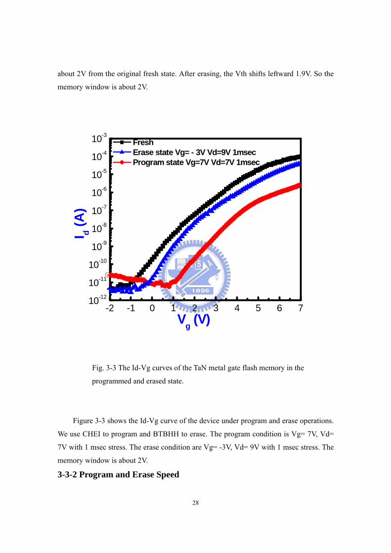

30
10-7 10-6 10-5 10-4 10-3 10-2 10-1 100
0
1
2
3
Initial Vt
Vg=-3V Vd=8V Vg=-4V Vd=8V Vg=-5V Vd=8V
V th
shi
ft (V
)
Erase Time (sec)
Fig 3-5 The erase speed curves of high-k CeO2 nanocrystal SONOS-type flash
memory with MoN metal gate
Figure 3-5 shows the erase speed of the MoN metal gate device For Vg= -3V -4V
and -5V with the same Vd =8V We can see all stress conditions the Vth shift gt 2V in
10msec The final erase state is below the initial state Therefore it shows no electron
back tunneling (EBT) and a little over-erase
For the high-k CeO2 nanocrystal SONOS-type flash memory with TaN metal gate
the program speed is shown in Fig3-6 We show three different stress conditions Vg=5V
Vd=5V Vg=6V Vd=6V Vg=7V Vd=7V As Fig 3-6 shows the condition Vg=7V Vd
=7V 1 msec cause Vth shift about 2V Its memory window is gt 5V
31
10-7 10-6 10-5 10-4 10-3 10-2 10-1 100
0
1
2
3
4
5 Vg=5V Vd=5V Vg=6V Vd=6V Vg=7V Vd=7V
V th
shi
ft (V
)
Program Time (sec)
Fig 3-6 The program speed curves of high-k CeO2 nanocrystal SONOS-type
flash memory with TaN metal gate
Figure 3-7 shows the erase speed of the TaN metal gate device For Vg= -3V -4V
and -5V with the same Vd=9V We can see all stress conditions the Vth shift gt 2V in
10msec And Vt shift of -2V can be achieved with Vg=-4 Vd=9V t lt1ms The final erase
state is below the initial state Because it has no electron back tunneling (EBT) so it
shows over-erase under large erase voltage (such as Vg= -4V Vd=9V and Vg=
-5V Vd=9V)
32
10-7 10-6 10-5 10-4 10-3 10-2 10-1 100-1
0
1
2
3
Initial Vt
Vg=-3V Vd=9V Vg=-4V Vd=9V Vg=-5V Vd=9V
V th
shi
ft (V
)
Erase Time (sec)
Fig 3-7 The erase speed curves of high-k CeO2 nanocrystal SONOS-type flash
memory with TaN metal gate
Figure 3-8 shows the erase speed of the N+-poly and MoN metal gate device To be
clearly understood EBT phenomenon we use F-N tunneling mechanism to erase For
N+-poly gate we can see a little Vth shift under small voltage (Vg=-15V) And EBT
phenomenon occurs when we apply large voltage to it (Vg=-18V) For MoN metal gate
it has no EBT under whether large nor small voltage It shows reasonable erase speed for
MoN metal gate device
33
10-7 10-6 10-5 10-4 10-3 10-2 10-1 1002
3
4
5
6
7
8 N+- poly gate Vg=-15V Vg=-18V
MoN gate Vg=-15V Vg=-18V
V th
shi
ft(V)
Erase Time(sec)
initial Vt
Fig 3-8 The erase speed curves of N+-poly and MoN gate CeO2 nanocrystal
memory with F-N tunneling mechanism
3-3-3 Data Retention Characteristic
Fig 3-9 is the data retention characteristic of MoN metal gate high-k CeO2
nanocrystal SONOS memory measured at 25oC We find the small charge loss with
time The curve shows only 5 charge loss as measure time up to 104 sec and 13
charge loss up to 108 sec at 25oC We infer the small charge loss at room temperature is
from the electron deep trap of high-k CeO2 nanocrystal We prove that sputtering MoN
and TaN metal will not damage the blocking oxide and CeO2 layer so it shows good
retention characteristic
34
100 101 102 103 104 105 106 107 1080
1
2
3
4
5
6
Initial Vt
retention at T=25oC
V th
(V)
Time (sec)
Fig 3-9 Retention characteristic of MoN metal gate high-k CeO2 nanocrystal
SONOS-type flash memory at 25OC
3-3-4 Disturbance Measurement Figure 3-10 shows the gate disturbance measurement of the MoN metal gate device
for three stress conditions Vg=7V Vg= 9V and Vg=11V with Vd =Vs=Vb=0V And
Figure 3-11 shows the gate disturbance measurement of the TaN metal gate device for
three stress conditions Vg=6V Vg= 8V and Vg=10V with Vd =Vs=Vb=0V The applied
gate voltage will attract electrons in the substrate tunneling to the CeO2 layer by FN
tunneling mechanism and result into Vth increase After 1000 sec stress the fresh state
Vth are almost the same It shows almost no gate disturbance after 1000 sec stress
35
100 101 102 103-2
-1
0
1
2
MoN Metal Vg=7V Vg=9V Vg=11V
Er
ase
stat
e V th
shi
ft (V
)
Gate Disturb Time (sec)
Fig 3-10 The gate disturbance characteristics of MoN metal gate device
100 101 102 103-20
-15
-10
-05
00
05
10
15
20
TaN Metal Vg=6V Vg=8V Vg=10V
Eras
e st
ate
V th s
hift
(V)
Gate Disturb Time (sec)
Fig 3-11 The gate disturbance characteristics of TaN metal gate device
36
Figure 3-12 shows the read disturbance measurement of the MoN metal gate device
And Figure 3-13 shows the read disturbance measurement of the TaN metal gate device
The measurement conditions are all fixed Vg=4V with different Vd= 2V 3V and 4V for
1000 sec stress The stress caused the fresh state Vth increase almost 0V It shows almost
no read disturbance after 1000 sec stress
100 101 102 103-2
-1
0
1
2
MoN Metal Vg=4V Vd=2V Vg=4V Vd=3V Vg=4V Vd=4V
Eras
e st
ate
V th s
hift
(V)
Read Disturb Time (sec)
Fig 3-12 The read disturbance characteristics of MoN metal gate device
37
100 101 102 103-2
-1
0
1
2
TaN Metal Vg=4V Vd=2V Vg=4V Vd=3V Vg=4V Vd=4V
Er
ase
stat
e V th
shi
ft (V
)
Read Disturb Time (sec)
Fig 3-13 The gate disturbance characteristics of TaN metal gate device
3-3-5 Physical Characteristics
Fig 3-14 shows the X-ray diffraction (XRD) characteristic of MoN metal gate
device The incident angle ranges from 15 degree to 60 degree We find signal intensity
peak appears at 3285 degree By searching the data base we find the rate between Mo
and N element is 11
Fig 3-15 shows the X-ray diffraction (XRD) characteristic of TaN metal gate device
The incident angle ranges from 15 degree to 60 degree We find signal intensity peak
appears at 33 degree By searching the data base we find the rate between Ta and N
element is 2086
38
20 30 40 50 600
500
1000
1500
2000
XRD Mo1N1
In
tens
ity (c
ps)
2 THETA (deg)
3285
Fig 3-14 The XRD characteristic of MoN metal gate device
28 30 32 34 36 380
5000
10000
15000
20000
XRD Ta2N086
Inte
nsity
(cps
)
2 THETA (deg)
33
Fig 3-15 The XRD characteristic of TaN metal gate device
39
Fig 3-16 The TEM image of MoN metal gate device
Fig 3-16 shows the cross-section-view high resolution tunneling electron
microscopy (HRTEM) of MoN metal gate device From the image the isolation of the
nanocrystals prevents the formation of effective conductive paths between adjacent nodes
The thickness of the tunnel oxide and blocking oxide are about 34nm and 154nm and
the thickness of the MoN metal is about 932nm The nanocrystal size ranges from 75nm
to 98nm
40
3-4 Summary In this chapter we replace conventional poly-Si gate with metal gate MoN TaN We
have shown the electric curves like Id-Vg program speed erase speed and small
disturbance We improve erase efficiency of high-k CeO2 nanocrystal memory with
different metal gates by using p-channel and n-channel devices We also demonstrate the
quality of high-k CeO2 nanocrystal with some good characteristics
41
3-5 Reference [1] Marvin H White Yang (Larry) Yang Ansha Purwar Margaret L Frenchrdquo A Low
Voltage SONOS Nonvolatile Semiconductor Memory Technology rdquo IEEE
transactions on components packaging and manufacturing technologymdashPART A
VOL 20 NO 2 JUNE 1997
[2] Shin-ichi Minami and Yoshiaki Kamigakirdquo A Novel MONOS Nonvolatile Memory
Device Ensuring 10-Year Data Retention after 107 EraseWrite Cycles rdquo IEEE
Transactions on Electron Devices VOL 40 NO 11 NOVEMBER 1993
[3] C C-H Hsu et al Exf Ah SSDM Tsukuba p 1401992
[4] T Ohnakado et al in IEDM Tech Dig p 2791995
[5] Jao-Hsian Shiue et al A study of interface trap generation by Fowler-Nordheim
and Substrate-hot-carrier stresses for 4-nm thick gate oxides in IEEE transactions
on electron devices vol 46 NO8 August 1999
[6] O Takahiro T Hiroshi K Hayashi and M D K Kaisha ldquoNon-volatile
semiconductor memory device capable of high speed programmingerasure US
patent no 5818761rdquo Oct 6 1998
[7] D P Shum et al ldquoA novel band-to-band tunneling induced convergence
mechanism for low current high density Flash EEPROM applicationsrdquo in IEDM
Tech Dig 1994 pp 41ndash44
[8] C-Y Hu et al ldquoSubstrate-current-induced hot electron (SCIHE) injection A new
convergence scheme for Flash memoryrdquo in IEDM Tech Dig 1995 pp 283ndash287
[9] T S Chen K H Wu H Chung and C H Kao ldquoperformance improvement of
SONOS memory by bandgap engineer of charge-trapping layerldquo IEEE Electron
42
Device Lett vol25 no4 pp 205-207 Apr 2002
[10] Marvin H White Yang (Larry) Yang Ansha Purwar Margaret L Frenchrdquo A
Low Voltage SONOS Nonvolatile Semiconductor Memory Technology rdquo IEEE
transactions on components packaging and manufacturing technologymdashPART A
VOL 20 NO 2 JUNE 1997
[11] T Sugizaki M Kohayashi M Ishidao H Minakata M Yamaguchi Y Tamura
Y Sugiyama T Nakanishi and H Tanakardquo Novel Multi-bit SONOS Type Flash
Memory Using a Highk Charge Trapping Layerrdquo Symposium on VLSl Technology
Digest of Technical Papers 2003
[12] Marvin H White Dennis A Adams James R Murray StephenWrazien Yijie
(Sandy) Zhao Yu (Richard) Wang Bilal Khan Wayne Miller Rajiv Mehrotra1rdquo
Characterization of Scaled SONOS EEPROM Memory Devices for Space and
Military Systems rdquo IEEE 2004
[13] G D Wilk R M Wallace J M Anthony rdquoHigh-k gate dielectrics Current status
and materials properties considerations rdquo Applied Physics Review vol89
no10pp5243-5275 Nay 2001
[14] T Ohnakado et al ldquoNovel electron injection method using band-to-band
tunneling induced hot electron (BBHE) for Flash memory with a p-channel cellrdquo
IEDM Tech Dig pp 279ndash282 1995
[15] T Ohnakado et al ldquoNovel self-limiting program scheme utilizing N-channel
select transistors in P-channel DINOR Flash memoryrdquo in IEDM Tech Dig 1996
pp 181ndash184
[16] S J Shen C S Yang Y S Wang and C C-H HsuldquoNovel self-convergent
programming scheme for multilevel P-channel Flash memoryrdquo in IEDM Tech
43
Dig 1997 pp 287ndash290
[17] R-L Lin Y-S Wang and C C-H HsuldquoP-channel Flash memoryrdquo in Proc
NVSMW 1998 pp 27ndash34
[18] T S-D Chang ldquoPMOS memory cell with hot electron injection programming and
tunneling erasing US Patent no 5687118rdquo Nov 11 1997
[19] T S-D Chang ldquoPMOS flash memory cell capable of multi-level threshold
voltage storage US Patent no 5666307rdquo Sept 9 1997
[20] T S-D Changldquonon-volatile electrically erasable memory with PMOS transistor
NAND gate structure US Patent no 5581504rdquo Dec 3 1996
[21] S J Shen C S Yang Y S Wang and C C-H HsuldquoNovel self-convergent
programming scheme for multilevel P-channel Flash memoryrdquo in IEDM Tech
Dig 1997 pp 287ndash290
[22] Frank Ruei-Ling Lin Yen-Sen Wang and Charles Ching-Hsiang Hsu
ldquoMulti-Level P-channel Flash Memoryrdquo pp457-463
[23] Steve S Chung S N Kuo C M Yih and T S Chao ldquoPerformance and
Reliability Evaluations of P-Channel Flash Memories with Different Programming
Schemesrdquo IEDM 97-295
[24] C C-H Hsu et al ldquoA high speed low power p-channel Flash EEPROM using
silicon rich oxide as tunneling dielectricrdquo in Proc Conf Solid State Devices and
Materials 1992 pp 140ndash141
44
Chapter 4
Characteristics of High-K CeO2 Nanocrystal
Memory with Different SourceDrain
Implantations
4-1 Introduction Recently SONOS-type memory has received considerable interest as one of the most
promising candidates to replace the conventional floating-gate flash memory Because as
the tunnel oxide thickness is scaled below 80 Aring the stress-induced leakage current (SILC)
has become such a severe problem that it will be a formidable challenge for floating-gate
devices to meet the ten-year retention requirement However for the SONOS device due
to its discrete charge trapping nature it is more robust to SILC since there is no lateral
charges movement to discharge the whole memory as one single defect is generated in
the tunnel oxide In addition SONOS memory has low operation voltage better
endurance and good compatibility with conventional CMOS process However
achieving fast programming and long retention at the same time remains to be one
challenge for SONOS devices Various approaches have been proposed for improving the
SONOS performance and reliability
In this work we purpose a high performance nonvolatile memory with high-k CeO2
nanocrystal charge trapping layer The serious leakage problem during retention can be
eliminated by utilizing a nanocrystal memory structure The electrons stored on the
nanocrystal directly above the defect chain will be affected since the nanocrystals are
separated from each other within the gate oxide dielectric The tunnel oxide thickness in
the nanocrystal memory device can be reduced to allow faster programming and lower
voltage operation We also use different sourcedrain implantation approaches to achieve
superior memory characteristics
45
4-2 Experimental Figure 4-1 schematically depicts the process flow of the proposed SONOS flash
memory
p-type Si substrate
LOCOSLOCOS
p-type Si substrate
LOCOSLOCOS
p-type Si substrate
LOCOSLOCOSTunneling oxide
CeO2 nanocrystal
Poly-Si Gate
Blocking oxide
p-type Si substrate
LOCOSLOCOSTunneling oxide
CeO2 nanocrystal
Poly-Si Gate
Blocking oxide
46
p-type Si substrate
Tunneling oxideCeO2 nanocrystal
Blocking Oxide
Poly-Si Gate
LOCOSLOCOS N+N+
p-type Si substrate
Tunneling oxideCeO2 nanocrystal
Blocking Oxide
Poly-Si Gate
LOCOSLOCOS N+N+
p-type Si substrate
Tunneling oxideCeO2 nanocrystal
Blocking Oxide
Poly-Si Gate
LOCOSLOCOS
metal
N+ N+
SiO2
p-type Si substrate
Tunneling oxideCeO2 nanocrystal
Blocking Oxide
Poly-Si Gate
LOCOSLOCOS
p-type Si substrate
Tunneling oxideCeO2 nanocrystal
Blocking Oxide
Poly-Si Gate
LOCOSLOCOS
p-type Si substrate
Tunneling oxideCeO2 nanocrystal
Blocking Oxide
Poly-Si Gate
LOCOSLOCOS
metal
N+ N+
SiO2
47
Fig 4-1 The process flow of the flash memory and the cross-section of the flash
memory (control samples)
The fabrication process of the CeO2 nanocrystal memory devices involved was
started with the LOCOS isolation process on p-type 5-10 Ω cm (100) 150mm silicon
substrates First a 2 nm thick tunnel oxide was thermally grown at 1000OC in vertical
furnace system The trapping layer of CeO2 layer was deposited by dual E-gun method
with CeO2 target After that the samples went through RTA treatment in O2 ambient at
900OC for 1 minute A blocking oxide of about 20 nm thick was then deposited by high
density plasma chemical vapor deposition (HDPCVD) After that the sample went
through RTA treatment in O2 ambient at 900OC for 1 minute Then a 200 nm thick
poly-silicon was deposited to serve as the gate electrode by LPCVD Then gate electrode
was patterned and the sourcedrain and gate were doped by self-aligned P ion
implantation at the dosage and energy of 5times1015 ionscm-2 and 25 KeV then the substrate
contact was patterned and the sub-contact was implanted with BF2 at the dosage and
energy of 5times1015 ionscm-2 and 40 KeV After these implantations the dopants were
activated at 950OC for 20 sec The rest of the subsequent standard CMOS procedures
were complete for fabricating the CeO2 high-k memory devices The above are control
samples
48
p-type Si substrate
Tunneling oxideCeO2 nanocrystal
Blocking Oxide
Poly-Si Gate
LOCOSLOCOS
BF2 ion implantation
p-type Si substrate
Tunneling oxideCeO2 nanocrystal
Blocking Oxide
Poly-Si Gate
LOCOSLOCOS
p-type Si substrate
Tunneling oxideCeO2 nanocrystal
Blocking Oxide
Poly-Si Gate
LOCOSLOCOS
BF2 ion implantation
p-type Si substrate
Tunneling oxideCeO2 nanocrystal
Blocking Oxide
Poly-Si Gate
LOCOSLOCOS
P31+ ion implantation
p-type Si substrate
Tunneling oxideCeO2 nanocrystal
Blocking Oxide
Poly-Si Gate
LOCOSLOCOSLOCOSLOCOS
P31+ ion implantation
49
p-type Si substrate
Tunneling oxideCeO2 nanocrystal
Blocking Oxide
Poly-Si Gate
LOCOSLOCOS N+N+ P+
p-type Si substrate
Tunneling oxideCeO2 nanocrystal
Blocking Oxide
Poly-Si Gate
LOCOSLOCOS N+N+ P+
p-type Si substrate
Tunneling oxideCeO2 nanocrystal
Blocking Oxide
Poly-Si Gate
LOCOSLOCOS
metal
N+ N+P+
SiO2
p-type Si substrate
Tunneling oxideCeO2 nanocrystal
Blocking Oxide
Poly-Si Gate
LOCOSLOCOS
p-type Si substrate
Tunneling oxideCeO2 nanocrystal
Blocking Oxide
Poly-Si Gate
LOCOSLOCOS
metal
N+ N+P+
SiO2
Fig 4-2 The process flow and the cross-section of the asymmetry sourcedrain
50
flash memory (asymmetry SD)
Figure 4-2 schematically depicts the process flow of the asymmetry sourcedrain
SONOS flash memory We changed the sourcedrain implantation with BF2 ion
implantation at the dosage and energy of 5times1013 ionscm-2 and 25 KeV (twist angle 72
degree tilt angle 30degree) then doped by P ion implantation at the dosage and energy
of 5times1015 ionscm-2 and 25 KeV (twist angle 0 degree tilt angle 0 degree) Then the
substrate contact was patterned and the sub-contact was implanted with BF2 at the dosage
and energy of 5times1015 ionscm-2 and 40 KeV After these implantations the dopants were
activated at 950OC for 20 sec The rest of the subsequent standard CMOS procedures
were complete for fabricating the CeO2 high-k memory devices
4-3 Results and Discussion In this section the electrical characteristics of high-k CeO2 nanocrystal SONOS-type
memory were discussed
4-3-1 Id-Vg Curve Figure 4-3 shows the Id-Vg curves of the device under program and erase
operations
51
2 3 4 5 6 7 8 9 101E-12
1E-11
1E-10
1E-9
1E-8
1E-7
1E-6
1E-5
1E-4
1E-3 Fresh Program state Vg=7V Vd=7V 10msec Erase state Vg=-4V Vd=8V 10msec
I d (A
)
Vg (V)
Fig 4-3 The Id-Vg curves of the high-k CeO2 nanocrystal SONOS-type flash
memory in the programmed and erase state
We use channel hot electron injection (CHEI) to program and band to band hot hole
to erase (BTBHH) The program condition is Vg= 7V Vd= 7V with 10 msec stress The
erase condition are Vg= -4V Vd= 8V with 10 msec stress The Vth after programming
shifts about 3V from the original fresh state After erasing the Vth shifts leftward about
27V So the memory window is about 3V We think the Vth shift rightward is due to
electron trapping in the high-k CeO2 nanocrystal layer The band offset is the reason why
trapping occurred During programming the electrons in the substrate gain energy from
the applied voltage Vg and Vd If the energy is enough to cross the energy barrier the hot
electrons will inject to the high-k CeO2 nanocrystal charge trapping layer and be trapped
This causes the Vth change When erasing we apply a negative gate voltage and positive
52
drain voltage to generate hot hole in the substrate If the hot hole in the substrate achieves
enough energy to cross the energy barrier it can reach the high-k CeO2 nanocrystal
charge trapping layer and cause the Id-Vg curve shift toward left
0 1 2 3 4 5 6 7 810-12
10-11
10-10
10-9
10-8
10-7
10-6
10-5
10-4
10-3
Fresh Program state Vg=7V Vd=7V 1msec Erase state Vg=-4V Vd=8V 10msec
I d (A
)
Vg (V)
Fig 4-4 The Id-Vg curves of the asymmetry sourcedrain high-k CeO2
nanocrystal SONOS-type flash memory
Figure 4-4 shows the Id-Vg curves of the device under program and erase operations
We use channel hot electron injection (CHEI) to program and band to band hot hole to
erase (BTBHH) The program condition is Vg= 7V Vd= 7V with 1 msec stress The erase
condition are Vg= -4V Vd= 8V with 10 msec stress The Vth after programming shifts
about 23V from the original fresh state After erasing the Vth shifts leftward about 23V
So the memory window is about 23V
4-3-2 Program and Erase Speed
53
For the control samples the program speed is shown in Fig 4-5
10-7 10-6 10-5 10-4 10-3 10-2 10-1 100
0
1
2
3
4
5
6 Vg=6V Vd=6V Vg=7V Vd=7V Vg=8V Vd=8V Vg=9V Vd=9V
V th s
hift
(V)
Program Time(sec)
Fig 4-5 The program speed curve of high-k CeO2 nanocrystal SONOS-type flash
memory
We show four different stress conditions Vg=6VVd=6V Vg=7VVd=7V
Vg=8VVd=8V Vg=9VVd=9V As Fig 4-5 shows the condition Vg=7V Vd=7V 1
msec cause Vth shift 2V and the condition Vg=8V Vd=8V 01 msec cause Vth shift 2V
With the Vg and Vd increasing the Vth shift also increases and the program speed is
faster memory window is gt 5V This is because as the gate voltage become more
positive for programming more hot electrons are generated So more and more hot
electrons can be trapped in the charge trapping layer Hence the Vth shift increases as
gate voltage and drain voltage increases
54
1E-7 1E-6 1E-5 1E-4 1E-3 001 01 10
1
2
3
4
5
6
7Vg Vs
Vg=6V Vd=6V Vg=7V Vd=7V Vg=8V Vd=8V
Vg Vd Vg=6V Vd=6V Vg=7V Vd=7V Vg=8V Vd=8V
V th s
hift(
V)
Program Time(sec)
Fig 4-6 The program speed curves of asymmetry sourcedrain high-k CeO2
nanocrystal SONOS-type flash memory
55
Fig 4-7 The band diagram of P+-N junction at reverse bias
Figure 4-6 shows the program speed of the asymmetry sourcedrain device First
define n-type only region as source define n-type and p-type region as drain We show
three different stress conditions Vg=6VVd=6V Vg=7VVd=7V Vg=8VVd=8V
compare with Vg=6VVs=6V Vg=7VVs=7V Vg=8VVs=8V As Fig 4-5 shows both
the condition Vg=7V Vd=7V and the condition Vg=7V Vs=7V 1 msec cause Vth shift
gt 2V With the Vg and VdVs increasing the Vth shift also increases and the program
speed is faster memory window is gt 6V Hence the Vth shift increases as gate voltage
and drain voltage source voltage increases When the drain voltage applies to the drain
region the p+-n junction is at reverse-biased condition so band bending becomes more
serious and then occurs zener breakdown as depicted in Fig 4-7 Therefore near drain
region more and more electron hole pairs generate so more and more hot electrons can
be trapped in the charge trapping layer In Fig 4-8 we prove high drain current under the
same drain and gate voltage the asymmetry sourcedrain device than the normal
sourcedrain device It means more and more electron hole pairs generate
Ec Ef Ev
P+ N
Vd
56
0 1 2 3 400
20x10-5
40x10-5
60x10-5
IdVd Vg-Vt=2V Vg-Vt=4V Vg-Vt=6V
IsVs Vg-Vt=2V Vg-Vt=4V Vg-Vt=6V
I d I s (V
)
Vd Vs (V)
Fig 4-8 The Id-Vd Is-Vs curves of the asymmetry sourcedrain high-k CeO2
nanocrystal SONOS-type flash memory
57
10-7 10-6 10-5 10-4 10-3 10-2 10-1 1000
1
2
3
4
5
6
7control
Vg=6V Vd=6V Vg=7V Vd=7V Vg=8V Vd=8V
changed Vg=6V Vd=6V Vg=7V Vd=7V Vg=8V Vd=8V
V th
shi
ft(V)
Program Time(sec)
Fig 4-9 The program speed curve of normal and asymmetry sourcedrain high-k
CeO2 nanocrystal SONOS-type flash memory
Figure 4-9 shows the program speed of the control device and asymmetry
sourcedrain device We show three different stress conditions Vg=6VVd=6V
Vg=7VVd=7V Vg=8VVd=8V With the Vg and VdVs increasing the Vth shift also
increases and the program speed is faster memory window is gt 6V Hence the Vth shift
increases as gate voltage and drain voltage increases Compared with control samples the
band bending of the p+-n junction at reverse-biased condition is more serious and occurs
zener breakdown Therefore more electron hole pairs generate more hot electrons can be
trapped in the charge trapping layer So the program speed of the asymmetry
sourcedrain device is faster than control device We prove this comment with Fig 4-10
58
0 1 2 3 400
20x10-5
40x10-5
60x10-5
control Vg-Vt=2V Vg-Vt=4V Vg-Vt=6V
changed Vg-Vt=2V Vg-Vt=4V Vg-Vt=6V
I d (V
)
Vd (V)
Fig 4-10 The Id-Vd curves of normal and asymmetry sourcedrain high-k CeO2
nanocrystal SONOS-type flash memory
Figure 4-11 shows the normalized erase speed of the device For Vg= -3V -4V and
-5V with the same Vd=8V We can see as the gate voltage becomes more negative the
Vth shift a little more and all stress conditions the Vth shift gt 25V in 10msec For Vd=
6V 7V and 8V with the same Vg= -4V We can see as the drain voltage becomes more
positive the Vth shift more Hence the Vth shift increases as gate voltage increases or
drain voltage increases Drain voltage influnces the erase speed is large than gate voltage
59
10-7 10-6 10-5 10-4 10-3 10-2 10-1 100-4
-3
-2
-1
0
Vg=-3V Vd=8V Vg=-4V Vd=8V Vg=-5V Vd=8V Vg=-4V Vd=6V Vg=-4V Vd=7V
V th s
hift(
V)
Erase Time(sec)
Fig 4-11 The erase speed curve of high-k CeO2 nanocrystal SONOS-type flash
memory
60
10-7 10-6 10-5 10-4 10-3 10-2 10-1 100
-4
-3
-2
-1
0
Vg Vs Vg=-4V Vd=6V Vg=-4V Vd=7V Vg=-4V Vd=8V
Vg Vd Vg=-4V Vd=6V Vg=-4V Vd=7V Vg=-4V Vd=8V
V th
shi
ft(V)
Erase Time(sec)
Fig 4-12 The erase speed curve of asymmetry sourcedrain high-k CeO2
nanocrystal SONOS-type flash memory
Figure 4-12 shows the normalized erase speed of the asymmetry sourcedrain device
For Vd= 6V 7V and 8V with the same Vg= -4V At low voltage (6V) the band
bending of high-dose P+-N junction at reversed bias is more serious than that of low-dose
P-N junction at reversed bias So more and more electron hole pairs generate near drain
region than that near source region The erase speed of condition Vg= -4V Vd= 6V is
more faster than condition Vg= -4V Vs= 6V At high voltage the band bending of
high-dose P+-N junction and low-dose P-N junction at reversed bias are all serious
Therefore the erase speeds of them are almost the same
Figure 4-13 shows the erase speed of the control device and asymmetry
sourcedrain device For Vd= 6V 7V and 8V with the same Vg= -4V This is also
61
because the band bending of high-dose P+-N junction (asymmetry sourcedrain) at
reversed bias is more serious than that of low-dose P-N junction (control samples) at
reversed bias Therefore the erase speed of the asymmetry sourcedrain device is faster
than control samples
10-7 10-6 10-5 10-4 10-3 10-2 10-1 100
-4
-3
-2
-1
0
control Vg=-4V Vd=6V Vg=-4V Vd=7V Vg=-4V Vd=8V
changed Vg=-4V Vd=6V Vg=-4V Vd=7V Vg=-4V Vd=8V
V th s
hift
(V)
Erase Time(sec)
Fig 4-13 The erase speed curves of normal and asymmetry sourcedrain high-k
CeO2 nanocrystal SONOS-type flash memory
62
4-3-3 Data Retention Characteristic Fig 4-14 is the data retention characteristic of high-k CeO2 nanocrystal SONOS
memory measured at 25oC We find the small charge loss with time The curve shows
only 85 charge loss as measure time up to 104 sec and 16 charge loss up to 108 sec at
25oC We infer the small charge loss at room temperature is from the electron deep trap of
high-k CeO2 nanocrystal charge trapping layer mentioned above
100 101 102 103 104 105 106 107 10800
05
10
15
20
25
30
35
40
Initial Vt
retention at T=25oC
V th (V
)
Time (sec)
Fig 4-14 Retention characteristic of the high-k CeO2 nanocrystal SONOS-type
flash memory at 25OC
63
4-3-4 Disturbance Measurement Figure 4-15 shows drain disturbance measurement of the normal and asymmetry
sourcedrain high-k CeO2 nanocrystal device We applied two stress conditions Vd =6V
and Vd=8V with Vg=Vs=Vb=0V to the device From the Fig 4-12 we can see little Vth
loss after 1000 sec stress for normal device the programmed state Vth loss is 015V at
Vd=6V and 023V for Vd=8V for the asymmetry sourcedrain device
100 101 102 103-03
-02
-01
00
01
02
03
Prog
ram
stat
e V
th sh
ift (V
)
Drain Disturb Time (sec)
controlVd=6V Vd=8V
changed Vd=6V Vd=8V
Fig 4-15 Drain disturbance characteristics of normal and asymmetry
sourcedrain high-k CeO2 nanocrystal SONOS-type flash memory
64
4-4 Summary In this chapter we propose a new sourcedrain implantation method for high-k CeO2
nanocrystal SONOS memory We have shown the electric curves like Id-Vg
programerase speed charge retention and drain disturbance We demonstrate the quality
of high-k CeO2 nanocrystal with some good characteristics in terms of large memory
window long charge retention time due to deep trap level in the CeO2 layer and small
drain disturbance
65
4-5 Reference [1] H Aozasa I Fujiwara A Nakamura and Y Komatsu ldquoAnalysis of Carrier Traps
in Si3N4 in OxideNitrideOxide for Metal OxideNitrideOxide Silicon Nonvolatile
Memoryrdquo Japanese Journal of Applied Physics Vol38 part 1 No 3A
pp1441-1447 1999
[2] Y Yang and M H White ldquoCharge retention of scaled SONOS nonvolatile
memory devices at elevated temperaturesrdquo Solid State Electronics Vol 44
pp949-958 2000
[3] YN Tan WK Chim BJ Cho and WK Choi ldquoOver-erase phenomenon in
SONOS-type flash memory and its minimization using a hafnium oxide charge
storage layerrdquo IEEE Trans Electron Devices vol 51 pp 1143-1147 July 2004
[4] G D Wilk R M Wallace and J M Anthony ldquoHigh-k gate dielectrics Current
status and materials properties considerationsrdquo Journal of Applied Physics Vol 89
pp 5243-5275 2001
[5] W Zhu TP Ma T Tamagawa Y Di J Kim R Carruthers M Gibson and T
Furukawa ldquoHfO2 and HfAlO for CMOS Thermal stability and current transportrdquo
in IEDM Tech Dig pp 463-466 2001
[6] S Ventkataraj O Kappertz C Liesch R Detemple R Jayavel M Wutting
Vacuum 75 7 (2004)
[7] W Zhao B K Tay G Q Yu S P Lau J Phys ndashCondens Mat 15 7707 (2003)
[8] A J Moulson and J M Herbert Electroceramics Wiley NJ (2003)
[9] W Zhu TP Ma T Tamagawa Y Di J Kim R Carruthers M Gibson T
Furukawa IEDM 463 (2001)
66
[10] M Balog M Schieber M Michman and S Patai Thin Solid films 47 190
(1997)
[11] M Balog and M Schieber J Electrochem Soc 1261203 (1979)
[12] WJ Tsai NK Zous CJ Liu CH Chen Tahui Wang Sam Pan and C-Y Lu
IEDM 719 (2001)
[13] Y-H Shih H-T Lue K-Y Hsieh Rich Liu and C-Y Lu IEDM 881 (2004)
[14] C T Swift G L Chindalore K Harber T S Harp A Hoefler C M Hong P
A Ingersoll C B Li E J Prinz and J A Yater IEDM 927 (2002)
67
Chapter 5
Conclusions The thesis of ldquoThe Study of High-K CeO2 Nanocrystal Flash Memory with
Different Metal Gates and SD Implantationsrdquo was proposed The results of each
chapter are summarized as below
In chapter 2 we discuss the dependence of metal gate work functions on the
different annealing temperatures We found a systematic methodology to extract the
accurate work function of metal gates We found the work function of TaN was about
46eV It located at the midgap of energy level so we choose a 700oC pre-annealing
step to densify metal and then treatment at 900OC for 20 sec to fabricate NMOS In
the other hand for MoN metal we choose a 600oC pre-annealing step to densify metal
and then treatment at 900OC for 20 sec to fabricate NMOS
In chapter 3 we replace conventional poly-Si gate with MoN and TaN metal
gates We have shown the electric curves like Id-Vg program speed erase speed and
disturbances We improve erase efficiency of high-k CeO2 nanocrystal memory with
different metal gates by using n-channel devices We also demonstrate the quality of
high-k CeO2 nanocrystal with some good characteristic in terms of large memory
window long charge retention time and small gate disturbance and read disturbance
In chapter 4 we propose a new sourcedrain implantation method to high-k CeO2
nanocrystal SONOS memory We have shown the electric curves like Id-Vg
programerase speedcharge retention and drain disturbance We demonstrate the
68
quality of high-k CeO2 nanocrystal with some good characteristics in terms of large
memory window long charge retention time due to deep trap level in the CeO2
nanocrystal and small drain disturbance
簡歷
姓 名 余 明 爵
性 別 男
出生日期 中華民國七十二年五月十一日
籍 貫 台灣省 桃園縣桃園市
地 址 桃園縣八德市廣德里 16 鄰順昌街 72 巷 1 號
學 歷 國立清華大學 工程與系統科學系
(民國 94 年 6 月)
國立交通大學 電子研究所固態組 碩士班
(民國 96 年 6 月)
論文題目 應用不同金屬閘極和源極汲極離子佈植於二氧化鈰
奈米微晶粒之 SONOS 記憶體研究
The Study of High-K CeO2 Nanocrystal Flash Memory
with Different Metal Gates and SourceDrain
Implantations
電子郵件u902131alumninthuedutw
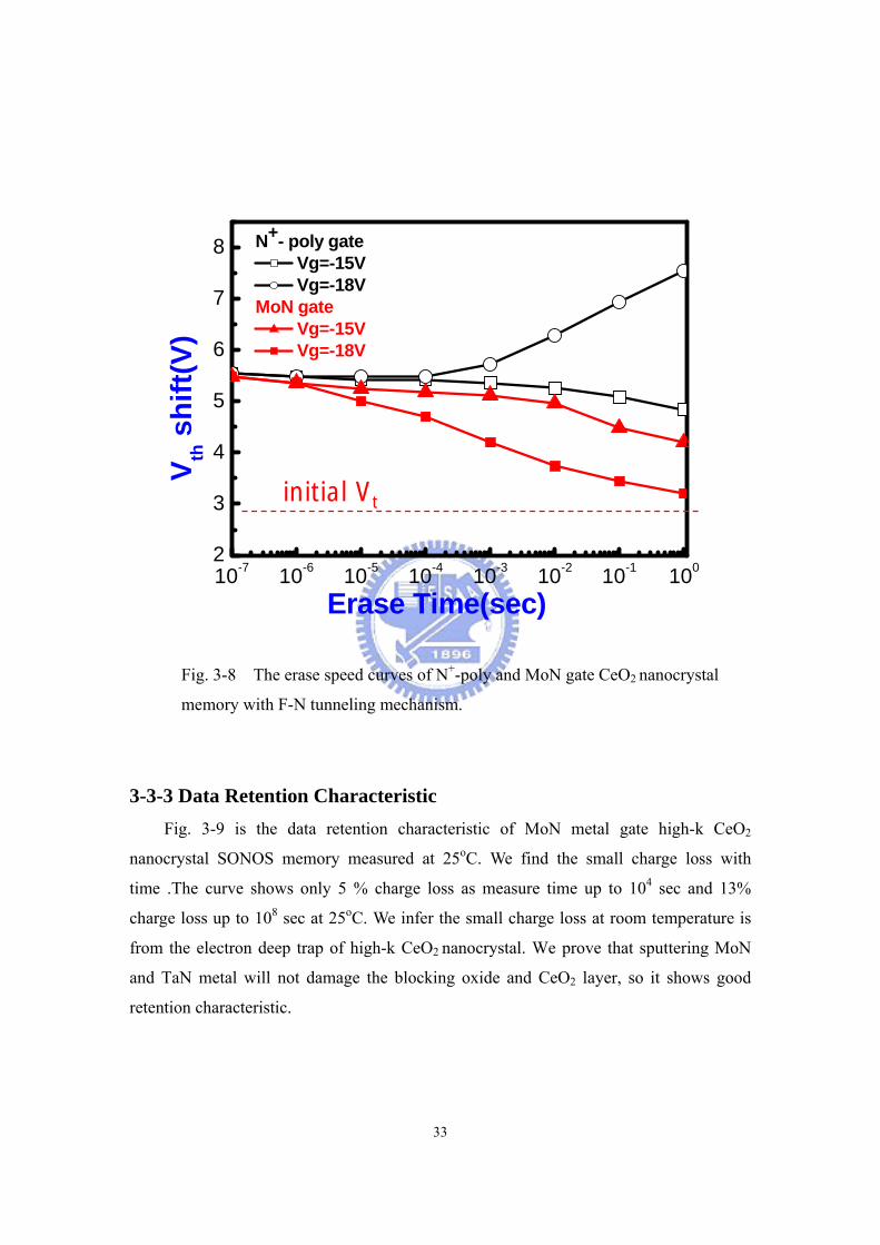
33
10-7 10-6 10-5 10-4 10-3 10-2 10-1 1002
3
4
5
6
7
8 N+- poly gate Vg=-15V Vg=-18V
MoN gate Vg=-15V Vg=-18V
V th
shi
ft(V)
Erase Time(sec)
initial Vt
Fig 3-8 The erase speed curves of N+-poly and MoN gate CeO2 nanocrystal
memory with F-N tunneling mechanism
3-3-3 Data Retention Characteristic
Fig 3-9 is the data retention characteristic of MoN metal gate high-k CeO2
nanocrystal SONOS memory measured at 25oC We find the small charge loss with
time The curve shows only 5 charge loss as measure time up to 104 sec and 13
charge loss up to 108 sec at 25oC We infer the small charge loss at room temperature is
from the electron deep trap of high-k CeO2 nanocrystal We prove that sputtering MoN
and TaN metal will not damage the blocking oxide and CeO2 layer so it shows good
retention characteristic
34
100 101 102 103 104 105 106 107 1080
1
2
3
4
5
6
Initial Vt
retention at T=25oC
V th
(V)
Time (sec)
Fig 3-9 Retention characteristic of MoN metal gate high-k CeO2 nanocrystal
SONOS-type flash memory at 25OC
3-3-4 Disturbance Measurement Figure 3-10 shows the gate disturbance measurement of the MoN metal gate device
for three stress conditions Vg=7V Vg= 9V and Vg=11V with Vd =Vs=Vb=0V And
Figure 3-11 shows the gate disturbance measurement of the TaN metal gate device for
three stress conditions Vg=6V Vg= 8V and Vg=10V with Vd =Vs=Vb=0V The applied
gate voltage will attract electrons in the substrate tunneling to the CeO2 layer by FN
tunneling mechanism and result into Vth increase After 1000 sec stress the fresh state
Vth are almost the same It shows almost no gate disturbance after 1000 sec stress
35
100 101 102 103-2
-1
0
1
2
MoN Metal Vg=7V Vg=9V Vg=11V
Er
ase
stat
e V th
shi
ft (V
)
Gate Disturb Time (sec)
Fig 3-10 The gate disturbance characteristics of MoN metal gate device
100 101 102 103-20
-15
-10
-05
00
05
10
15
20
TaN Metal Vg=6V Vg=8V Vg=10V
Eras
e st
ate
V th s
hift
(V)
Gate Disturb Time (sec)
Fig 3-11 The gate disturbance characteristics of TaN metal gate device
36
Figure 3-12 shows the read disturbance measurement of the MoN metal gate device
And Figure 3-13 shows the read disturbance measurement of the TaN metal gate device
The measurement conditions are all fixed Vg=4V with different Vd= 2V 3V and 4V for
1000 sec stress The stress caused the fresh state Vth increase almost 0V It shows almost
no read disturbance after 1000 sec stress
100 101 102 103-2
-1
0
1
2
MoN Metal Vg=4V Vd=2V Vg=4V Vd=3V Vg=4V Vd=4V
Eras
e st
ate
V th s
hift
(V)
Read Disturb Time (sec)
Fig 3-12 The read disturbance characteristics of MoN metal gate device
37
100 101 102 103-2
-1
0
1
2
TaN Metal Vg=4V Vd=2V Vg=4V Vd=3V Vg=4V Vd=4V
Er
ase
stat
e V th
shi
ft (V
)
Read Disturb Time (sec)
Fig 3-13 The gate disturbance characteristics of TaN metal gate device
3-3-5 Physical Characteristics
Fig 3-14 shows the X-ray diffraction (XRD) characteristic of MoN metal gate
device The incident angle ranges from 15 degree to 60 degree We find signal intensity
peak appears at 3285 degree By searching the data base we find the rate between Mo
and N element is 11
Fig 3-15 shows the X-ray diffraction (XRD) characteristic of TaN metal gate device
The incident angle ranges from 15 degree to 60 degree We find signal intensity peak
appears at 33 degree By searching the data base we find the rate between Ta and N
element is 2086
38
20 30 40 50 600
500
1000
1500
2000
XRD Mo1N1
In
tens
ity (c
ps)
2 THETA (deg)
3285
Fig 3-14 The XRD characteristic of MoN metal gate device
28 30 32 34 36 380
5000
10000
15000
20000
XRD Ta2N086
Inte
nsity
(cps
)
2 THETA (deg)
33
Fig 3-15 The XRD characteristic of TaN metal gate device
39
Fig 3-16 The TEM image of MoN metal gate device
Fig 3-16 shows the cross-section-view high resolution tunneling electron
microscopy (HRTEM) of MoN metal gate device From the image the isolation of the
nanocrystals prevents the formation of effective conductive paths between adjacent nodes
The thickness of the tunnel oxide and blocking oxide are about 34nm and 154nm and
the thickness of the MoN metal is about 932nm The nanocrystal size ranges from 75nm
to 98nm
40
3-4 Summary In this chapter we replace conventional poly-Si gate with metal gate MoN TaN We
have shown the electric curves like Id-Vg program speed erase speed and small
disturbance We improve erase efficiency of high-k CeO2 nanocrystal memory with
different metal gates by using p-channel and n-channel devices We also demonstrate the
quality of high-k CeO2 nanocrystal with some good characteristics
41
3-5 Reference [1] Marvin H White Yang (Larry) Yang Ansha Purwar Margaret L Frenchrdquo A Low
Voltage SONOS Nonvolatile Semiconductor Memory Technology rdquo IEEE
transactions on components packaging and manufacturing technologymdashPART A
VOL 20 NO 2 JUNE 1997
[2] Shin-ichi Minami and Yoshiaki Kamigakirdquo A Novel MONOS Nonvolatile Memory
Device Ensuring 10-Year Data Retention after 107 EraseWrite Cycles rdquo IEEE
Transactions on Electron Devices VOL 40 NO 11 NOVEMBER 1993
[3] C C-H Hsu et al Exf Ah SSDM Tsukuba p 1401992
[4] T Ohnakado et al in IEDM Tech Dig p 2791995
[5] Jao-Hsian Shiue et al A study of interface trap generation by Fowler-Nordheim
and Substrate-hot-carrier stresses for 4-nm thick gate oxides in IEEE transactions
on electron devices vol 46 NO8 August 1999
[6] O Takahiro T Hiroshi K Hayashi and M D K Kaisha ldquoNon-volatile
semiconductor memory device capable of high speed programmingerasure US
patent no 5818761rdquo Oct 6 1998
[7] D P Shum et al ldquoA novel band-to-band tunneling induced convergence
mechanism for low current high density Flash EEPROM applicationsrdquo in IEDM
Tech Dig 1994 pp 41ndash44
[8] C-Y Hu et al ldquoSubstrate-current-induced hot electron (SCIHE) injection A new
convergence scheme for Flash memoryrdquo in IEDM Tech Dig 1995 pp 283ndash287
[9] T S Chen K H Wu H Chung and C H Kao ldquoperformance improvement of
SONOS memory by bandgap engineer of charge-trapping layerldquo IEEE Electron
42
Device Lett vol25 no4 pp 205-207 Apr 2002
[10] Marvin H White Yang (Larry) Yang Ansha Purwar Margaret L Frenchrdquo A
Low Voltage SONOS Nonvolatile Semiconductor Memory Technology rdquo IEEE
transactions on components packaging and manufacturing technologymdashPART A
VOL 20 NO 2 JUNE 1997
[11] T Sugizaki M Kohayashi M Ishidao H Minakata M Yamaguchi Y Tamura
Y Sugiyama T Nakanishi and H Tanakardquo Novel Multi-bit SONOS Type Flash
Memory Using a Highk Charge Trapping Layerrdquo Symposium on VLSl Technology
Digest of Technical Papers 2003
[12] Marvin H White Dennis A Adams James R Murray StephenWrazien Yijie
(Sandy) Zhao Yu (Richard) Wang Bilal Khan Wayne Miller Rajiv Mehrotra1rdquo
Characterization of Scaled SONOS EEPROM Memory Devices for Space and
Military Systems rdquo IEEE 2004
[13] G D Wilk R M Wallace J M Anthony rdquoHigh-k gate dielectrics Current status
and materials properties considerations rdquo Applied Physics Review vol89
no10pp5243-5275 Nay 2001
[14] T Ohnakado et al ldquoNovel electron injection method using band-to-band
tunneling induced hot electron (BBHE) for Flash memory with a p-channel cellrdquo
IEDM Tech Dig pp 279ndash282 1995
[15] T Ohnakado et al ldquoNovel self-limiting program scheme utilizing N-channel
select transistors in P-channel DINOR Flash memoryrdquo in IEDM Tech Dig 1996
pp 181ndash184
[16] S J Shen C S Yang Y S Wang and C C-H HsuldquoNovel self-convergent
programming scheme for multilevel P-channel Flash memoryrdquo in IEDM Tech
43
Dig 1997 pp 287ndash290
[17] R-L Lin Y-S Wang and C C-H HsuldquoP-channel Flash memoryrdquo in Proc
NVSMW 1998 pp 27ndash34
[18] T S-D Chang ldquoPMOS memory cell with hot electron injection programming and
tunneling erasing US Patent no 5687118rdquo Nov 11 1997
[19] T S-D Chang ldquoPMOS flash memory cell capable of multi-level threshold
voltage storage US Patent no 5666307rdquo Sept 9 1997
[20] T S-D Changldquonon-volatile electrically erasable memory with PMOS transistor
NAND gate structure US Patent no 5581504rdquo Dec 3 1996
[21] S J Shen C S Yang Y S Wang and C C-H HsuldquoNovel self-convergent
programming scheme for multilevel P-channel Flash memoryrdquo in IEDM Tech
Dig 1997 pp 287ndash290
[22] Frank Ruei-Ling Lin Yen-Sen Wang and Charles Ching-Hsiang Hsu
ldquoMulti-Level P-channel Flash Memoryrdquo pp457-463
[23] Steve S Chung S N Kuo C M Yih and T S Chao ldquoPerformance and
Reliability Evaluations of P-Channel Flash Memories with Different Programming
Schemesrdquo IEDM 97-295
[24] C C-H Hsu et al ldquoA high speed low power p-channel Flash EEPROM using
silicon rich oxide as tunneling dielectricrdquo in Proc Conf Solid State Devices and
Materials 1992 pp 140ndash141
44
Chapter 4
Characteristics of High-K CeO2 Nanocrystal
Memory with Different SourceDrain
Implantations
4-1 Introduction Recently SONOS-type memory has received considerable interest as one of the most
promising candidates to replace the conventional floating-gate flash memory Because as
the tunnel oxide thickness is scaled below 80 Aring the stress-induced leakage current (SILC)
has become such a severe problem that it will be a formidable challenge for floating-gate
devices to meet the ten-year retention requirement However for the SONOS device due
to its discrete charge trapping nature it is more robust to SILC since there is no lateral
charges movement to discharge the whole memory as one single defect is generated in
the tunnel oxide In addition SONOS memory has low operation voltage better
endurance and good compatibility with conventional CMOS process However
achieving fast programming and long retention at the same time remains to be one
challenge for SONOS devices Various approaches have been proposed for improving the
SONOS performance and reliability
In this work we purpose a high performance nonvolatile memory with high-k CeO2
nanocrystal charge trapping layer The serious leakage problem during retention can be
eliminated by utilizing a nanocrystal memory structure The electrons stored on the
nanocrystal directly above the defect chain will be affected since the nanocrystals are
separated from each other within the gate oxide dielectric The tunnel oxide thickness in
the nanocrystal memory device can be reduced to allow faster programming and lower
voltage operation We also use different sourcedrain implantation approaches to achieve
superior memory characteristics
45
4-2 Experimental Figure 4-1 schematically depicts the process flow of the proposed SONOS flash
memory
p-type Si substrate
LOCOSLOCOS
p-type Si substrate
LOCOSLOCOS
p-type Si substrate
LOCOSLOCOSTunneling oxide
CeO2 nanocrystal
Poly-Si Gate
Blocking oxide
p-type Si substrate
LOCOSLOCOSTunneling oxide
CeO2 nanocrystal
Poly-Si Gate
Blocking oxide
46
p-type Si substrate
Tunneling oxideCeO2 nanocrystal
Blocking Oxide
Poly-Si Gate
LOCOSLOCOS N+N+
p-type Si substrate
Tunneling oxideCeO2 nanocrystal
Blocking Oxide
Poly-Si Gate
LOCOSLOCOS N+N+
p-type Si substrate
Tunneling oxideCeO2 nanocrystal
Blocking Oxide
Poly-Si Gate
LOCOSLOCOS
metal
N+ N+
SiO2
p-type Si substrate
Tunneling oxideCeO2 nanocrystal
Blocking Oxide
Poly-Si Gate
LOCOSLOCOS
p-type Si substrate
Tunneling oxideCeO2 nanocrystal
Blocking Oxide
Poly-Si Gate
LOCOSLOCOS
p-type Si substrate
Tunneling oxideCeO2 nanocrystal
Blocking Oxide
Poly-Si Gate
LOCOSLOCOS
metal
N+ N+
SiO2
47
Fig 4-1 The process flow of the flash memory and the cross-section of the flash
memory (control samples)
The fabrication process of the CeO2 nanocrystal memory devices involved was
started with the LOCOS isolation process on p-type 5-10 Ω cm (100) 150mm silicon
substrates First a 2 nm thick tunnel oxide was thermally grown at 1000OC in vertical
furnace system The trapping layer of CeO2 layer was deposited by dual E-gun method
with CeO2 target After that the samples went through RTA treatment in O2 ambient at
900OC for 1 minute A blocking oxide of about 20 nm thick was then deposited by high
density plasma chemical vapor deposition (HDPCVD) After that the sample went
through RTA treatment in O2 ambient at 900OC for 1 minute Then a 200 nm thick
poly-silicon was deposited to serve as the gate electrode by LPCVD Then gate electrode
was patterned and the sourcedrain and gate were doped by self-aligned P ion
implantation at the dosage and energy of 5times1015 ionscm-2 and 25 KeV then the substrate
contact was patterned and the sub-contact was implanted with BF2 at the dosage and
energy of 5times1015 ionscm-2 and 40 KeV After these implantations the dopants were
activated at 950OC for 20 sec The rest of the subsequent standard CMOS procedures
were complete for fabricating the CeO2 high-k memory devices The above are control
samples
48
p-type Si substrate
Tunneling oxideCeO2 nanocrystal
Blocking Oxide
Poly-Si Gate
LOCOSLOCOS
BF2 ion implantation
p-type Si substrate
Tunneling oxideCeO2 nanocrystal
Blocking Oxide
Poly-Si Gate
LOCOSLOCOS
p-type Si substrate
Tunneling oxideCeO2 nanocrystal
Blocking Oxide
Poly-Si Gate
LOCOSLOCOS
BF2 ion implantation
p-type Si substrate
Tunneling oxideCeO2 nanocrystal
Blocking Oxide
Poly-Si Gate
LOCOSLOCOS
P31+ ion implantation
p-type Si substrate
Tunneling oxideCeO2 nanocrystal
Blocking Oxide
Poly-Si Gate
LOCOSLOCOSLOCOSLOCOS
P31+ ion implantation
49
p-type Si substrate
Tunneling oxideCeO2 nanocrystal
Blocking Oxide
Poly-Si Gate
LOCOSLOCOS N+N+ P+
p-type Si substrate
Tunneling oxideCeO2 nanocrystal
Blocking Oxide
Poly-Si Gate
LOCOSLOCOS N+N+ P+
p-type Si substrate
Tunneling oxideCeO2 nanocrystal
Blocking Oxide
Poly-Si Gate
LOCOSLOCOS
metal
N+ N+P+
SiO2
p-type Si substrate
Tunneling oxideCeO2 nanocrystal
Blocking Oxide
Poly-Si Gate
LOCOSLOCOS
p-type Si substrate
Tunneling oxideCeO2 nanocrystal
Blocking Oxide
Poly-Si Gate
LOCOSLOCOS
metal
N+ N+P+
SiO2
Fig 4-2 The process flow and the cross-section of the asymmetry sourcedrain
50
flash memory (asymmetry SD)
Figure 4-2 schematically depicts the process flow of the asymmetry sourcedrain
SONOS flash memory We changed the sourcedrain implantation with BF2 ion
implantation at the dosage and energy of 5times1013 ionscm-2 and 25 KeV (twist angle 72
degree tilt angle 30degree) then doped by P ion implantation at the dosage and energy
of 5times1015 ionscm-2 and 25 KeV (twist angle 0 degree tilt angle 0 degree) Then the
substrate contact was patterned and the sub-contact was implanted with BF2 at the dosage
and energy of 5times1015 ionscm-2 and 40 KeV After these implantations the dopants were
activated at 950OC for 20 sec The rest of the subsequent standard CMOS procedures
were complete for fabricating the CeO2 high-k memory devices
4-3 Results and Discussion In this section the electrical characteristics of high-k CeO2 nanocrystal SONOS-type
memory were discussed
4-3-1 Id-Vg Curve Figure 4-3 shows the Id-Vg curves of the device under program and erase
operations
51
2 3 4 5 6 7 8 9 101E-12
1E-11
1E-10
1E-9
1E-8
1E-7
1E-6
1E-5
1E-4
1E-3 Fresh Program state Vg=7V Vd=7V 10msec Erase state Vg=-4V Vd=8V 10msec
I d (A
)
Vg (V)
Fig 4-3 The Id-Vg curves of the high-k CeO2 nanocrystal SONOS-type flash
memory in the programmed and erase state
We use channel hot electron injection (CHEI) to program and band to band hot hole
to erase (BTBHH) The program condition is Vg= 7V Vd= 7V with 10 msec stress The
erase condition are Vg= -4V Vd= 8V with 10 msec stress The Vth after programming
shifts about 3V from the original fresh state After erasing the Vth shifts leftward about
27V So the memory window is about 3V We think the Vth shift rightward is due to
electron trapping in the high-k CeO2 nanocrystal layer The band offset is the reason why
trapping occurred During programming the electrons in the substrate gain energy from
the applied voltage Vg and Vd If the energy is enough to cross the energy barrier the hot
electrons will inject to the high-k CeO2 nanocrystal charge trapping layer and be trapped
This causes the Vth change When erasing we apply a negative gate voltage and positive
52
drain voltage to generate hot hole in the substrate If the hot hole in the substrate achieves
enough energy to cross the energy barrier it can reach the high-k CeO2 nanocrystal
charge trapping layer and cause the Id-Vg curve shift toward left
0 1 2 3 4 5 6 7 810-12
10-11
10-10
10-9
10-8
10-7
10-6
10-5
10-4
10-3
Fresh Program state Vg=7V Vd=7V 1msec Erase state Vg=-4V Vd=8V 10msec
I d (A
)
Vg (V)
Fig 4-4 The Id-Vg curves of the asymmetry sourcedrain high-k CeO2
nanocrystal SONOS-type flash memory
Figure 4-4 shows the Id-Vg curves of the device under program and erase operations
We use channel hot electron injection (CHEI) to program and band to band hot hole to
erase (BTBHH) The program condition is Vg= 7V Vd= 7V with 1 msec stress The erase
condition are Vg= -4V Vd= 8V with 10 msec stress The Vth after programming shifts
about 23V from the original fresh state After erasing the Vth shifts leftward about 23V
So the memory window is about 23V
4-3-2 Program and Erase Speed
53
For the control samples the program speed is shown in Fig 4-5
10-7 10-6 10-5 10-4 10-3 10-2 10-1 100
0
1
2
3
4
5
6 Vg=6V Vd=6V Vg=7V Vd=7V Vg=8V Vd=8V Vg=9V Vd=9V
V th s
hift
(V)
Program Time(sec)
Fig 4-5 The program speed curve of high-k CeO2 nanocrystal SONOS-type flash
memory
We show four different stress conditions Vg=6VVd=6V Vg=7VVd=7V
Vg=8VVd=8V Vg=9VVd=9V As Fig 4-5 shows the condition Vg=7V Vd=7V 1
msec cause Vth shift 2V and the condition Vg=8V Vd=8V 01 msec cause Vth shift 2V
With the Vg and Vd increasing the Vth shift also increases and the program speed is
faster memory window is gt 5V This is because as the gate voltage become more
positive for programming more hot electrons are generated So more and more hot
electrons can be trapped in the charge trapping layer Hence the Vth shift increases as
gate voltage and drain voltage increases
54
1E-7 1E-6 1E-5 1E-4 1E-3 001 01 10
1
2
3
4
5
6
7Vg Vs
Vg=6V Vd=6V Vg=7V Vd=7V Vg=8V Vd=8V
Vg Vd Vg=6V Vd=6V Vg=7V Vd=7V Vg=8V Vd=8V
V th s
hift(
V)
Program Time(sec)
Fig 4-6 The program speed curves of asymmetry sourcedrain high-k CeO2
nanocrystal SONOS-type flash memory
55
Fig 4-7 The band diagram of P+-N junction at reverse bias
Figure 4-6 shows the program speed of the asymmetry sourcedrain device First
define n-type only region as source define n-type and p-type region as drain We show
three different stress conditions Vg=6VVd=6V Vg=7VVd=7V Vg=8VVd=8V
compare with Vg=6VVs=6V Vg=7VVs=7V Vg=8VVs=8V As Fig 4-5 shows both
the condition Vg=7V Vd=7V and the condition Vg=7V Vs=7V 1 msec cause Vth shift
gt 2V With the Vg and VdVs increasing the Vth shift also increases and the program
speed is faster memory window is gt 6V Hence the Vth shift increases as gate voltage
and drain voltage source voltage increases When the drain voltage applies to the drain
region the p+-n junction is at reverse-biased condition so band bending becomes more
serious and then occurs zener breakdown as depicted in Fig 4-7 Therefore near drain
region more and more electron hole pairs generate so more and more hot electrons can
be trapped in the charge trapping layer In Fig 4-8 we prove high drain current under the
same drain and gate voltage the asymmetry sourcedrain device than the normal
sourcedrain device It means more and more electron hole pairs generate
Ec Ef Ev
P+ N
Vd
56
0 1 2 3 400
20x10-5
40x10-5
60x10-5
IdVd Vg-Vt=2V Vg-Vt=4V Vg-Vt=6V
IsVs Vg-Vt=2V Vg-Vt=4V Vg-Vt=6V
I d I s (V
)
Vd Vs (V)
Fig 4-8 The Id-Vd Is-Vs curves of the asymmetry sourcedrain high-k CeO2
nanocrystal SONOS-type flash memory
57
10-7 10-6 10-5 10-4 10-3 10-2 10-1 1000
1
2
3
4
5
6
7control
Vg=6V Vd=6V Vg=7V Vd=7V Vg=8V Vd=8V
changed Vg=6V Vd=6V Vg=7V Vd=7V Vg=8V Vd=8V
V th
shi
ft(V)
Program Time(sec)
Fig 4-9 The program speed curve of normal and asymmetry sourcedrain high-k
CeO2 nanocrystal SONOS-type flash memory
Figure 4-9 shows the program speed of the control device and asymmetry
sourcedrain device We show three different stress conditions Vg=6VVd=6V
Vg=7VVd=7V Vg=8VVd=8V With the Vg and VdVs increasing the Vth shift also
increases and the program speed is faster memory window is gt 6V Hence the Vth shift
increases as gate voltage and drain voltage increases Compared with control samples the
band bending of the p+-n junction at reverse-biased condition is more serious and occurs
zener breakdown Therefore more electron hole pairs generate more hot electrons can be
trapped in the charge trapping layer So the program speed of the asymmetry
sourcedrain device is faster than control device We prove this comment with Fig 4-10
58
0 1 2 3 400
20x10-5
40x10-5
60x10-5
control Vg-Vt=2V Vg-Vt=4V Vg-Vt=6V
changed Vg-Vt=2V Vg-Vt=4V Vg-Vt=6V
I d (V
)
Vd (V)
Fig 4-10 The Id-Vd curves of normal and asymmetry sourcedrain high-k CeO2
nanocrystal SONOS-type flash memory
Figure 4-11 shows the normalized erase speed of the device For Vg= -3V -4V and
-5V with the same Vd=8V We can see as the gate voltage becomes more negative the
Vth shift a little more and all stress conditions the Vth shift gt 25V in 10msec For Vd=
6V 7V and 8V with the same Vg= -4V We can see as the drain voltage becomes more
positive the Vth shift more Hence the Vth shift increases as gate voltage increases or
drain voltage increases Drain voltage influnces the erase speed is large than gate voltage
59
10-7 10-6 10-5 10-4 10-3 10-2 10-1 100-4
-3
-2
-1
0
Vg=-3V Vd=8V Vg=-4V Vd=8V Vg=-5V Vd=8V Vg=-4V Vd=6V Vg=-4V Vd=7V
V th s
hift(
V)
Erase Time(sec)
Fig 4-11 The erase speed curve of high-k CeO2 nanocrystal SONOS-type flash
memory
60
10-7 10-6 10-5 10-4 10-3 10-2 10-1 100
-4
-3
-2
-1
0
Vg Vs Vg=-4V Vd=6V Vg=-4V Vd=7V Vg=-4V Vd=8V
Vg Vd Vg=-4V Vd=6V Vg=-4V Vd=7V Vg=-4V Vd=8V
V th
shi
ft(V)
Erase Time(sec)
Fig 4-12 The erase speed curve of asymmetry sourcedrain high-k CeO2
nanocrystal SONOS-type flash memory
Figure 4-12 shows the normalized erase speed of the asymmetry sourcedrain device
For Vd= 6V 7V and 8V with the same Vg= -4V At low voltage (6V) the band
bending of high-dose P+-N junction at reversed bias is more serious than that of low-dose
P-N junction at reversed bias So more and more electron hole pairs generate near drain
region than that near source region The erase speed of condition Vg= -4V Vd= 6V is
more faster than condition Vg= -4V Vs= 6V At high voltage the band bending of
high-dose P+-N junction and low-dose P-N junction at reversed bias are all serious
Therefore the erase speeds of them are almost the same
Figure 4-13 shows the erase speed of the control device and asymmetry
sourcedrain device For Vd= 6V 7V and 8V with the same Vg= -4V This is also
61
because the band bending of high-dose P+-N junction (asymmetry sourcedrain) at
reversed bias is more serious than that of low-dose P-N junction (control samples) at
reversed bias Therefore the erase speed of the asymmetry sourcedrain device is faster
than control samples
10-7 10-6 10-5 10-4 10-3 10-2 10-1 100
-4
-3
-2
-1
0
control Vg=-4V Vd=6V Vg=-4V Vd=7V Vg=-4V Vd=8V
changed Vg=-4V Vd=6V Vg=-4V Vd=7V Vg=-4V Vd=8V
V th s
hift
(V)
Erase Time(sec)
Fig 4-13 The erase speed curves of normal and asymmetry sourcedrain high-k
CeO2 nanocrystal SONOS-type flash memory
62
4-3-3 Data Retention Characteristic Fig 4-14 is the data retention characteristic of high-k CeO2 nanocrystal SONOS
memory measured at 25oC We find the small charge loss with time The curve shows
only 85 charge loss as measure time up to 104 sec and 16 charge loss up to 108 sec at
25oC We infer the small charge loss at room temperature is from the electron deep trap of
high-k CeO2 nanocrystal charge trapping layer mentioned above
100 101 102 103 104 105 106 107 10800
05
10
15
20
25
30
35
40
Initial Vt
retention at T=25oC
V th (V
)
Time (sec)
Fig 4-14 Retention characteristic of the high-k CeO2 nanocrystal SONOS-type
flash memory at 25OC
63
4-3-4 Disturbance Measurement Figure 4-15 shows drain disturbance measurement of the normal and asymmetry
sourcedrain high-k CeO2 nanocrystal device We applied two stress conditions Vd =6V
and Vd=8V with Vg=Vs=Vb=0V to the device From the Fig 4-12 we can see little Vth
loss after 1000 sec stress for normal device the programmed state Vth loss is 015V at
Vd=6V and 023V for Vd=8V for the asymmetry sourcedrain device
100 101 102 103-03
-02
-01
00
01
02
03
Prog
ram
stat
e V
th sh
ift (V
)
Drain Disturb Time (sec)
controlVd=6V Vd=8V
changed Vd=6V Vd=8V
Fig 4-15 Drain disturbance characteristics of normal and asymmetry
sourcedrain high-k CeO2 nanocrystal SONOS-type flash memory
64
4-4 Summary In this chapter we propose a new sourcedrain implantation method for high-k CeO2
nanocrystal SONOS memory We have shown the electric curves like Id-Vg
programerase speed charge retention and drain disturbance We demonstrate the quality
of high-k CeO2 nanocrystal with some good characteristics in terms of large memory
window long charge retention time due to deep trap level in the CeO2 layer and small
drain disturbance
65
4-5 Reference [1] H Aozasa I Fujiwara A Nakamura and Y Komatsu ldquoAnalysis of Carrier Traps
in Si3N4 in OxideNitrideOxide for Metal OxideNitrideOxide Silicon Nonvolatile
Memoryrdquo Japanese Journal of Applied Physics Vol38 part 1 No 3A
pp1441-1447 1999
[2] Y Yang and M H White ldquoCharge retention of scaled SONOS nonvolatile
memory devices at elevated temperaturesrdquo Solid State Electronics Vol 44
pp949-958 2000
[3] YN Tan WK Chim BJ Cho and WK Choi ldquoOver-erase phenomenon in
SONOS-type flash memory and its minimization using a hafnium oxide charge
storage layerrdquo IEEE Trans Electron Devices vol 51 pp 1143-1147 July 2004
[4] G D Wilk R M Wallace and J M Anthony ldquoHigh-k gate dielectrics Current
status and materials properties considerationsrdquo Journal of Applied Physics Vol 89
pp 5243-5275 2001
[5] W Zhu TP Ma T Tamagawa Y Di J Kim R Carruthers M Gibson and T
Furukawa ldquoHfO2 and HfAlO for CMOS Thermal stability and current transportrdquo
in IEDM Tech Dig pp 463-466 2001
[6] S Ventkataraj O Kappertz C Liesch R Detemple R Jayavel M Wutting
Vacuum 75 7 (2004)
[7] W Zhao B K Tay G Q Yu S P Lau J Phys ndashCondens Mat 15 7707 (2003)
[8] A J Moulson and J M Herbert Electroceramics Wiley NJ (2003)
[9] W Zhu TP Ma T Tamagawa Y Di J Kim R Carruthers M Gibson T
Furukawa IEDM 463 (2001)
66
[10] M Balog M Schieber M Michman and S Patai Thin Solid films 47 190
(1997)
[11] M Balog and M Schieber J Electrochem Soc 1261203 (1979)
[12] WJ Tsai NK Zous CJ Liu CH Chen Tahui Wang Sam Pan and C-Y Lu
IEDM 719 (2001)
[13] Y-H Shih H-T Lue K-Y Hsieh Rich Liu and C-Y Lu IEDM 881 (2004)
[14] C T Swift G L Chindalore K Harber T S Harp A Hoefler C M Hong P
A Ingersoll C B Li E J Prinz and J A Yater IEDM 927 (2002)
67
Chapter 5
Conclusions The thesis of ldquoThe Study of High-K CeO2 Nanocrystal Flash Memory with
Different Metal Gates and SD Implantationsrdquo was proposed The results of each
chapter are summarized as below
In chapter 2 we discuss the dependence of metal gate work functions on the
different annealing temperatures We found a systematic methodology to extract the
accurate work function of metal gates We found the work function of TaN was about
46eV It located at the midgap of energy level so we choose a 700oC pre-annealing
step to densify metal and then treatment at 900OC for 20 sec to fabricate NMOS In
the other hand for MoN metal we choose a 600oC pre-annealing step to densify metal
and then treatment at 900OC for 20 sec to fabricate NMOS
In chapter 3 we replace conventional poly-Si gate with MoN and TaN metal
gates We have shown the electric curves like Id-Vg program speed erase speed and
disturbances We improve erase efficiency of high-k CeO2 nanocrystal memory with
different metal gates by using n-channel devices We also demonstrate the quality of
high-k CeO2 nanocrystal with some good characteristic in terms of large memory
window long charge retention time and small gate disturbance and read disturbance
In chapter 4 we propose a new sourcedrain implantation method to high-k CeO2
nanocrystal SONOS memory We have shown the electric curves like Id-Vg
programerase speedcharge retention and drain disturbance We demonstrate the
68
quality of high-k CeO2 nanocrystal with some good characteristics in terms of large
memory window long charge retention time due to deep trap level in the CeO2
nanocrystal and small drain disturbance
簡歷
姓 名 余 明 爵
性 別 男
出生日期 中華民國七十二年五月十一日
籍 貫 台灣省 桃園縣桃園市
地 址 桃園縣八德市廣德里 16 鄰順昌街 72 巷 1 號
學 歷 國立清華大學 工程與系統科學系
(民國 94 年 6 月)
國立交通大學 電子研究所固態組 碩士班
(民國 96 年 6 月)
論文題目 應用不同金屬閘極和源極汲極離子佈植於二氧化鈰
奈米微晶粒之 SONOS 記憶體研究
The Study of High-K CeO2 Nanocrystal Flash Memory
with Different Metal Gates and SourceDrain
Implantations
電子郵件u902131alumninthuedutw

35
100 101 102 103-2
-1
0
1
2
MoN Metal Vg=7V Vg=9V Vg=11V
Er
ase
stat
e V th
shi
ft (V
)
Gate Disturb Time (sec)
Fig 3-10 The gate disturbance characteristics of MoN metal gate device
100 101 102 103-20
-15
-10
-05
00
05
10
15
20
TaN Metal Vg=6V Vg=8V Vg=10V
Eras
e st
ate
V th s
hift
(V)
Gate Disturb Time (sec)
Fig 3-11 The gate disturbance characteristics of TaN metal gate device
36
Figure 3-12 shows the read disturbance measurement of the MoN metal gate device
And Figure 3-13 shows the read disturbance measurement of the TaN metal gate device
The measurement conditions are all fixed Vg=4V with different Vd= 2V 3V and 4V for
1000 sec stress The stress caused the fresh state Vth increase almost 0V It shows almost
no read disturbance after 1000 sec stress
100 101 102 103-2
-1
0
1
2
MoN Metal Vg=4V Vd=2V Vg=4V Vd=3V Vg=4V Vd=4V
Eras
e st
ate
V th s
hift
(V)
Read Disturb Time (sec)
Fig 3-12 The read disturbance characteristics of MoN metal gate device
37
100 101 102 103-2
-1
0
1
2
TaN Metal Vg=4V Vd=2V Vg=4V Vd=3V Vg=4V Vd=4V
Er
ase
stat
e V th
shi
ft (V
)
Read Disturb Time (sec)
Fig 3-13 The gate disturbance characteristics of TaN metal gate device
3-3-5 Physical Characteristics
Fig 3-14 shows the X-ray diffraction (XRD) characteristic of MoN metal gate
device The incident angle ranges from 15 degree to 60 degree We find signal intensity
peak appears at 3285 degree By searching the data base we find the rate between Mo
and N element is 11
Fig 3-15 shows the X-ray diffraction (XRD) characteristic of TaN metal gate device
The incident angle ranges from 15 degree to 60 degree We find signal intensity peak
appears at 33 degree By searching the data base we find the rate between Ta and N
element is 2086
38
20 30 40 50 600
500
1000
1500
2000
XRD Mo1N1
In
tens
ity (c
ps)
2 THETA (deg)
3285
Fig 3-14 The XRD characteristic of MoN metal gate device
28 30 32 34 36 380
5000
10000
15000
20000
XRD Ta2N086
Inte
nsity
(cps
)
2 THETA (deg)
33
Fig 3-15 The XRD characteristic of TaN metal gate device
39
Fig 3-16 The TEM image of MoN metal gate device
Fig 3-16 shows the cross-section-view high resolution tunneling electron
microscopy (HRTEM) of MoN metal gate device From the image the isolation of the
nanocrystals prevents the formation of effective conductive paths between adjacent nodes
The thickness of the tunnel oxide and blocking oxide are about 34nm and 154nm and
the thickness of the MoN metal is about 932nm The nanocrystal size ranges from 75nm
to 98nm
40
3-4 Summary In this chapter we replace conventional poly-Si gate with metal gate MoN TaN We
have shown the electric curves like Id-Vg program speed erase speed and small
disturbance We improve erase efficiency of high-k CeO2 nanocrystal memory with
different metal gates by using p-channel and n-channel devices We also demonstrate the
quality of high-k CeO2 nanocrystal with some good characteristics
41
3-5 Reference [1] Marvin H White Yang (Larry) Yang Ansha Purwar Margaret L Frenchrdquo A Low
Voltage SONOS Nonvolatile Semiconductor Memory Technology rdquo IEEE
transactions on components packaging and manufacturing technologymdashPART A
VOL 20 NO 2 JUNE 1997
[2] Shin-ichi Minami and Yoshiaki Kamigakirdquo A Novel MONOS Nonvolatile Memory
Device Ensuring 10-Year Data Retention after 107 EraseWrite Cycles rdquo IEEE
Transactions on Electron Devices VOL 40 NO 11 NOVEMBER 1993
[3] C C-H Hsu et al Exf Ah SSDM Tsukuba p 1401992
[4] T Ohnakado et al in IEDM Tech Dig p 2791995
[5] Jao-Hsian Shiue et al A study of interface trap generation by Fowler-Nordheim
and Substrate-hot-carrier stresses for 4-nm thick gate oxides in IEEE transactions
on electron devices vol 46 NO8 August 1999
[6] O Takahiro T Hiroshi K Hayashi and M D K Kaisha ldquoNon-volatile
semiconductor memory device capable of high speed programmingerasure US
patent no 5818761rdquo Oct 6 1998
[7] D P Shum et al ldquoA novel band-to-band tunneling induced convergence
mechanism for low current high density Flash EEPROM applicationsrdquo in IEDM
Tech Dig 1994 pp 41ndash44
[8] C-Y Hu et al ldquoSubstrate-current-induced hot electron (SCIHE) injection A new
convergence scheme for Flash memoryrdquo in IEDM Tech Dig 1995 pp 283ndash287
[9] T S Chen K H Wu H Chung and C H Kao ldquoperformance improvement of
SONOS memory by bandgap engineer of charge-trapping layerldquo IEEE Electron
42
Device Lett vol25 no4 pp 205-207 Apr 2002
[10] Marvin H White Yang (Larry) Yang Ansha Purwar Margaret L Frenchrdquo A
Low Voltage SONOS Nonvolatile Semiconductor Memory Technology rdquo IEEE
transactions on components packaging and manufacturing technologymdashPART A
VOL 20 NO 2 JUNE 1997
[11] T Sugizaki M Kohayashi M Ishidao H Minakata M Yamaguchi Y Tamura
Y Sugiyama T Nakanishi and H Tanakardquo Novel Multi-bit SONOS Type Flash
Memory Using a Highk Charge Trapping Layerrdquo Symposium on VLSl Technology
Digest of Technical Papers 2003
[12] Marvin H White Dennis A Adams James R Murray StephenWrazien Yijie
(Sandy) Zhao Yu (Richard) Wang Bilal Khan Wayne Miller Rajiv Mehrotra1rdquo
Characterization of Scaled SONOS EEPROM Memory Devices for Space and
Military Systems rdquo IEEE 2004
[13] G D Wilk R M Wallace J M Anthony rdquoHigh-k gate dielectrics Current status
and materials properties considerations rdquo Applied Physics Review vol89
no10pp5243-5275 Nay 2001
[14] T Ohnakado et al ldquoNovel electron injection method using band-to-band
tunneling induced hot electron (BBHE) for Flash memory with a p-channel cellrdquo
IEDM Tech Dig pp 279ndash282 1995
[15] T Ohnakado et al ldquoNovel self-limiting program scheme utilizing N-channel
select transistors in P-channel DINOR Flash memoryrdquo in IEDM Tech Dig 1996
pp 181ndash184
[16] S J Shen C S Yang Y S Wang and C C-H HsuldquoNovel self-convergent
programming scheme for multilevel P-channel Flash memoryrdquo in IEDM Tech
43
Dig 1997 pp 287ndash290
[17] R-L Lin Y-S Wang and C C-H HsuldquoP-channel Flash memoryrdquo in Proc
NVSMW 1998 pp 27ndash34
[18] T S-D Chang ldquoPMOS memory cell with hot electron injection programming and
tunneling erasing US Patent no 5687118rdquo Nov 11 1997
[19] T S-D Chang ldquoPMOS flash memory cell capable of multi-level threshold
voltage storage US Patent no 5666307rdquo Sept 9 1997
[20] T S-D Changldquonon-volatile electrically erasable memory with PMOS transistor
NAND gate structure US Patent no 5581504rdquo Dec 3 1996
[21] S J Shen C S Yang Y S Wang and C C-H HsuldquoNovel self-convergent
programming scheme for multilevel P-channel Flash memoryrdquo in IEDM Tech
Dig 1997 pp 287ndash290
[22] Frank Ruei-Ling Lin Yen-Sen Wang and Charles Ching-Hsiang Hsu
ldquoMulti-Level P-channel Flash Memoryrdquo pp457-463
[23] Steve S Chung S N Kuo C M Yih and T S Chao ldquoPerformance and
Reliability Evaluations of P-Channel Flash Memories with Different Programming
Schemesrdquo IEDM 97-295
[24] C C-H Hsu et al ldquoA high speed low power p-channel Flash EEPROM using
silicon rich oxide as tunneling dielectricrdquo in Proc Conf Solid State Devices and
Materials 1992 pp 140ndash141
44
Chapter 4
Characteristics of High-K CeO2 Nanocrystal
Memory with Different SourceDrain
Implantations
4-1 Introduction Recently SONOS-type memory has received considerable interest as one of the most
promising candidates to replace the conventional floating-gate flash memory Because as
the tunnel oxide thickness is scaled below 80 Aring the stress-induced leakage current (SILC)
has become such a severe problem that it will be a formidable challenge for floating-gate
devices to meet the ten-year retention requirement However for the SONOS device due
to its discrete charge trapping nature it is more robust to SILC since there is no lateral
charges movement to discharge the whole memory as one single defect is generated in
the tunnel oxide In addition SONOS memory has low operation voltage better
endurance and good compatibility with conventional CMOS process However
achieving fast programming and long retention at the same time remains to be one
challenge for SONOS devices Various approaches have been proposed for improving the
SONOS performance and reliability
In this work we purpose a high performance nonvolatile memory with high-k CeO2
nanocrystal charge trapping layer The serious leakage problem during retention can be
eliminated by utilizing a nanocrystal memory structure The electrons stored on the
nanocrystal directly above the defect chain will be affected since the nanocrystals are
separated from each other within the gate oxide dielectric The tunnel oxide thickness in
the nanocrystal memory device can be reduced to allow faster programming and lower
voltage operation We also use different sourcedrain implantation approaches to achieve
superior memory characteristics
45
4-2 Experimental Figure 4-1 schematically depicts the process flow of the proposed SONOS flash
memory
p-type Si substrate
LOCOSLOCOS
p-type Si substrate
LOCOSLOCOS
p-type Si substrate
LOCOSLOCOSTunneling oxide
CeO2 nanocrystal
Poly-Si Gate
Blocking oxide
p-type Si substrate
LOCOSLOCOSTunneling oxide
CeO2 nanocrystal
Poly-Si Gate
Blocking oxide
46
p-type Si substrate
Tunneling oxideCeO2 nanocrystal
Blocking Oxide
Poly-Si Gate
LOCOSLOCOS N+N+
p-type Si substrate
Tunneling oxideCeO2 nanocrystal
Blocking Oxide
Poly-Si Gate
LOCOSLOCOS N+N+
p-type Si substrate
Tunneling oxideCeO2 nanocrystal
Blocking Oxide
Poly-Si Gate
LOCOSLOCOS
metal
N+ N+
SiO2
p-type Si substrate
Tunneling oxideCeO2 nanocrystal
Blocking Oxide
Poly-Si Gate
LOCOSLOCOS
p-type Si substrate
Tunneling oxideCeO2 nanocrystal
Blocking Oxide
Poly-Si Gate
LOCOSLOCOS
p-type Si substrate
Tunneling oxideCeO2 nanocrystal
Blocking Oxide
Poly-Si Gate
LOCOSLOCOS
metal
N+ N+
SiO2
47
Fig 4-1 The process flow of the flash memory and the cross-section of the flash
memory (control samples)
The fabrication process of the CeO2 nanocrystal memory devices involved was
started with the LOCOS isolation process on p-type 5-10 Ω cm (100) 150mm silicon
substrates First a 2 nm thick tunnel oxide was thermally grown at 1000OC in vertical
furnace system The trapping layer of CeO2 layer was deposited by dual E-gun method
with CeO2 target After that the samples went through RTA treatment in O2 ambient at
900OC for 1 minute A blocking oxide of about 20 nm thick was then deposited by high
density plasma chemical vapor deposition (HDPCVD) After that the sample went
through RTA treatment in O2 ambient at 900OC for 1 minute Then a 200 nm thick
poly-silicon was deposited to serve as the gate electrode by LPCVD Then gate electrode
was patterned and the sourcedrain and gate were doped by self-aligned P ion
implantation at the dosage and energy of 5times1015 ionscm-2 and 25 KeV then the substrate
contact was patterned and the sub-contact was implanted with BF2 at the dosage and
energy of 5times1015 ionscm-2 and 40 KeV After these implantations the dopants were
activated at 950OC for 20 sec The rest of the subsequent standard CMOS procedures
were complete for fabricating the CeO2 high-k memory devices The above are control
samples
48
p-type Si substrate
Tunneling oxideCeO2 nanocrystal
Blocking Oxide
Poly-Si Gate
LOCOSLOCOS
BF2 ion implantation
p-type Si substrate
Tunneling oxideCeO2 nanocrystal
Blocking Oxide
Poly-Si Gate
LOCOSLOCOS
p-type Si substrate
Tunneling oxideCeO2 nanocrystal
Blocking Oxide
Poly-Si Gate
LOCOSLOCOS
BF2 ion implantation
p-type Si substrate
Tunneling oxideCeO2 nanocrystal
Blocking Oxide
Poly-Si Gate
LOCOSLOCOS
P31+ ion implantation
p-type Si substrate
Tunneling oxideCeO2 nanocrystal
Blocking Oxide
Poly-Si Gate
LOCOSLOCOSLOCOSLOCOS
P31+ ion implantation
49
p-type Si substrate
Tunneling oxideCeO2 nanocrystal
Blocking Oxide
Poly-Si Gate
LOCOSLOCOS N+N+ P+
p-type Si substrate
Tunneling oxideCeO2 nanocrystal
Blocking Oxide
Poly-Si Gate
LOCOSLOCOS N+N+ P+
p-type Si substrate
Tunneling oxideCeO2 nanocrystal
Blocking Oxide
Poly-Si Gate
LOCOSLOCOS
metal
N+ N+P+
SiO2
p-type Si substrate
Tunneling oxideCeO2 nanocrystal
Blocking Oxide
Poly-Si Gate
LOCOSLOCOS
p-type Si substrate
Tunneling oxideCeO2 nanocrystal
Blocking Oxide
Poly-Si Gate
LOCOSLOCOS
metal
N+ N+P+
SiO2
Fig 4-2 The process flow and the cross-section of the asymmetry sourcedrain
50
flash memory (asymmetry SD)
Figure 4-2 schematically depicts the process flow of the asymmetry sourcedrain
SONOS flash memory We changed the sourcedrain implantation with BF2 ion
implantation at the dosage and energy of 5times1013 ionscm-2 and 25 KeV (twist angle 72
degree tilt angle 30degree) then doped by P ion implantation at the dosage and energy
of 5times1015 ionscm-2 and 25 KeV (twist angle 0 degree tilt angle 0 degree) Then the
substrate contact was patterned and the sub-contact was implanted with BF2 at the dosage
and energy of 5times1015 ionscm-2 and 40 KeV After these implantations the dopants were
activated at 950OC for 20 sec The rest of the subsequent standard CMOS procedures
were complete for fabricating the CeO2 high-k memory devices
4-3 Results and Discussion In this section the electrical characteristics of high-k CeO2 nanocrystal SONOS-type
memory were discussed
4-3-1 Id-Vg Curve Figure 4-3 shows the Id-Vg curves of the device under program and erase
operations
51
2 3 4 5 6 7 8 9 101E-12
1E-11
1E-10
1E-9
1E-8
1E-7
1E-6
1E-5
1E-4
1E-3 Fresh Program state Vg=7V Vd=7V 10msec Erase state Vg=-4V Vd=8V 10msec
I d (A
)
Vg (V)
Fig 4-3 The Id-Vg curves of the high-k CeO2 nanocrystal SONOS-type flash
memory in the programmed and erase state
We use channel hot electron injection (CHEI) to program and band to band hot hole
to erase (BTBHH) The program condition is Vg= 7V Vd= 7V with 10 msec stress The
erase condition are Vg= -4V Vd= 8V with 10 msec stress The Vth after programming
shifts about 3V from the original fresh state After erasing the Vth shifts leftward about
27V So the memory window is about 3V We think the Vth shift rightward is due to
electron trapping in the high-k CeO2 nanocrystal layer The band offset is the reason why
trapping occurred During programming the electrons in the substrate gain energy from
the applied voltage Vg and Vd If the energy is enough to cross the energy barrier the hot
electrons will inject to the high-k CeO2 nanocrystal charge trapping layer and be trapped
This causes the Vth change When erasing we apply a negative gate voltage and positive
52
drain voltage to generate hot hole in the substrate If the hot hole in the substrate achieves
enough energy to cross the energy barrier it can reach the high-k CeO2 nanocrystal
charge trapping layer and cause the Id-Vg curve shift toward left
0 1 2 3 4 5 6 7 810-12
10-11
10-10
10-9
10-8
10-7
10-6
10-5
10-4
10-3
Fresh Program state Vg=7V Vd=7V 1msec Erase state Vg=-4V Vd=8V 10msec
I d (A
)
Vg (V)
Fig 4-4 The Id-Vg curves of the asymmetry sourcedrain high-k CeO2
nanocrystal SONOS-type flash memory
Figure 4-4 shows the Id-Vg curves of the device under program and erase operations
We use channel hot electron injection (CHEI) to program and band to band hot hole to
erase (BTBHH) The program condition is Vg= 7V Vd= 7V with 1 msec stress The erase
condition are Vg= -4V Vd= 8V with 10 msec stress The Vth after programming shifts
about 23V from the original fresh state After erasing the Vth shifts leftward about 23V
So the memory window is about 23V
4-3-2 Program and Erase Speed
53
For the control samples the program speed is shown in Fig 4-5
10-7 10-6 10-5 10-4 10-3 10-2 10-1 100
0
1
2
3
4
5
6 Vg=6V Vd=6V Vg=7V Vd=7V Vg=8V Vd=8V Vg=9V Vd=9V
V th s
hift
(V)
Program Time(sec)
Fig 4-5 The program speed curve of high-k CeO2 nanocrystal SONOS-type flash
memory
We show four different stress conditions Vg=6VVd=6V Vg=7VVd=7V
Vg=8VVd=8V Vg=9VVd=9V As Fig 4-5 shows the condition Vg=7V Vd=7V 1
msec cause Vth shift 2V and the condition Vg=8V Vd=8V 01 msec cause Vth shift 2V
With the Vg and Vd increasing the Vth shift also increases and the program speed is
faster memory window is gt 5V This is because as the gate voltage become more
positive for programming more hot electrons are generated So more and more hot
electrons can be trapped in the charge trapping layer Hence the Vth shift increases as
gate voltage and drain voltage increases
54
1E-7 1E-6 1E-5 1E-4 1E-3 001 01 10
1
2
3
4
5
6
7Vg Vs
Vg=6V Vd=6V Vg=7V Vd=7V Vg=8V Vd=8V
Vg Vd Vg=6V Vd=6V Vg=7V Vd=7V Vg=8V Vd=8V
V th s
hift(
V)
Program Time(sec)
Fig 4-6 The program speed curves of asymmetry sourcedrain high-k CeO2
nanocrystal SONOS-type flash memory
55
Fig 4-7 The band diagram of P+-N junction at reverse bias
Figure 4-6 shows the program speed of the asymmetry sourcedrain device First
define n-type only region as source define n-type and p-type region as drain We show
three different stress conditions Vg=6VVd=6V Vg=7VVd=7V Vg=8VVd=8V
compare with Vg=6VVs=6V Vg=7VVs=7V Vg=8VVs=8V As Fig 4-5 shows both
the condition Vg=7V Vd=7V and the condition Vg=7V Vs=7V 1 msec cause Vth shift
gt 2V With the Vg and VdVs increasing the Vth shift also increases and the program
speed is faster memory window is gt 6V Hence the Vth shift increases as gate voltage
and drain voltage source voltage increases When the drain voltage applies to the drain
region the p+-n junction is at reverse-biased condition so band bending becomes more
serious and then occurs zener breakdown as depicted in Fig 4-7 Therefore near drain
region more and more electron hole pairs generate so more and more hot electrons can
be trapped in the charge trapping layer In Fig 4-8 we prove high drain current under the
same drain and gate voltage the asymmetry sourcedrain device than the normal
sourcedrain device It means more and more electron hole pairs generate
Ec Ef Ev
P+ N
Vd
56
0 1 2 3 400
20x10-5
40x10-5
60x10-5
IdVd Vg-Vt=2V Vg-Vt=4V Vg-Vt=6V
IsVs Vg-Vt=2V Vg-Vt=4V Vg-Vt=6V
I d I s (V
)
Vd Vs (V)
Fig 4-8 The Id-Vd Is-Vs curves of the asymmetry sourcedrain high-k CeO2
nanocrystal SONOS-type flash memory
57
10-7 10-6 10-5 10-4 10-3 10-2 10-1 1000
1
2
3
4
5
6
7control
Vg=6V Vd=6V Vg=7V Vd=7V Vg=8V Vd=8V
changed Vg=6V Vd=6V Vg=7V Vd=7V Vg=8V Vd=8V
V th
shi
ft(V)
Program Time(sec)
Fig 4-9 The program speed curve of normal and asymmetry sourcedrain high-k
CeO2 nanocrystal SONOS-type flash memory
Figure 4-9 shows the program speed of the control device and asymmetry
sourcedrain device We show three different stress conditions Vg=6VVd=6V
Vg=7VVd=7V Vg=8VVd=8V With the Vg and VdVs increasing the Vth shift also
increases and the program speed is faster memory window is gt 6V Hence the Vth shift
increases as gate voltage and drain voltage increases Compared with control samples the
band bending of the p+-n junction at reverse-biased condition is more serious and occurs
zener breakdown Therefore more electron hole pairs generate more hot electrons can be
trapped in the charge trapping layer So the program speed of the asymmetry
sourcedrain device is faster than control device We prove this comment with Fig 4-10
58
0 1 2 3 400
20x10-5
40x10-5
60x10-5
control Vg-Vt=2V Vg-Vt=4V Vg-Vt=6V
changed Vg-Vt=2V Vg-Vt=4V Vg-Vt=6V
I d (V
)
Vd (V)
Fig 4-10 The Id-Vd curves of normal and asymmetry sourcedrain high-k CeO2
nanocrystal SONOS-type flash memory
Figure 4-11 shows the normalized erase speed of the device For Vg= -3V -4V and
-5V with the same Vd=8V We can see as the gate voltage becomes more negative the
Vth shift a little more and all stress conditions the Vth shift gt 25V in 10msec For Vd=
6V 7V and 8V with the same Vg= -4V We can see as the drain voltage becomes more
positive the Vth shift more Hence the Vth shift increases as gate voltage increases or
drain voltage increases Drain voltage influnces the erase speed is large than gate voltage
59
10-7 10-6 10-5 10-4 10-3 10-2 10-1 100-4
-3
-2
-1
0
Vg=-3V Vd=8V Vg=-4V Vd=8V Vg=-5V Vd=8V Vg=-4V Vd=6V Vg=-4V Vd=7V
V th s
hift(
V)
Erase Time(sec)
Fig 4-11 The erase speed curve of high-k CeO2 nanocrystal SONOS-type flash
memory
60
10-7 10-6 10-5 10-4 10-3 10-2 10-1 100
-4
-3
-2
-1
0
Vg Vs Vg=-4V Vd=6V Vg=-4V Vd=7V Vg=-4V Vd=8V
Vg Vd Vg=-4V Vd=6V Vg=-4V Vd=7V Vg=-4V Vd=8V
V th
shi
ft(V)
Erase Time(sec)
Fig 4-12 The erase speed curve of asymmetry sourcedrain high-k CeO2
nanocrystal SONOS-type flash memory
Figure 4-12 shows the normalized erase speed of the asymmetry sourcedrain device
For Vd= 6V 7V and 8V with the same Vg= -4V At low voltage (6V) the band
bending of high-dose P+-N junction at reversed bias is more serious than that of low-dose
P-N junction at reversed bias So more and more electron hole pairs generate near drain
region than that near source region The erase speed of condition Vg= -4V Vd= 6V is
more faster than condition Vg= -4V Vs= 6V At high voltage the band bending of
high-dose P+-N junction and low-dose P-N junction at reversed bias are all serious
Therefore the erase speeds of them are almost the same
Figure 4-13 shows the erase speed of the control device and asymmetry
sourcedrain device For Vd= 6V 7V and 8V with the same Vg= -4V This is also
61
because the band bending of high-dose P+-N junction (asymmetry sourcedrain) at
reversed bias is more serious than that of low-dose P-N junction (control samples) at
reversed bias Therefore the erase speed of the asymmetry sourcedrain device is faster
than control samples
10-7 10-6 10-5 10-4 10-3 10-2 10-1 100
-4
-3
-2
-1
0
control Vg=-4V Vd=6V Vg=-4V Vd=7V Vg=-4V Vd=8V
changed Vg=-4V Vd=6V Vg=-4V Vd=7V Vg=-4V Vd=8V
V th s
hift
(V)
Erase Time(sec)
Fig 4-13 The erase speed curves of normal and asymmetry sourcedrain high-k
CeO2 nanocrystal SONOS-type flash memory
62
4-3-3 Data Retention Characteristic Fig 4-14 is the data retention characteristic of high-k CeO2 nanocrystal SONOS
memory measured at 25oC We find the small charge loss with time The curve shows
only 85 charge loss as measure time up to 104 sec and 16 charge loss up to 108 sec at
25oC We infer the small charge loss at room temperature is from the electron deep trap of
high-k CeO2 nanocrystal charge trapping layer mentioned above
100 101 102 103 104 105 106 107 10800
05
10
15
20
25
30
35
40
Initial Vt
retention at T=25oC
V th (V
)
Time (sec)
Fig 4-14 Retention characteristic of the high-k CeO2 nanocrystal SONOS-type
flash memory at 25OC
63
4-3-4 Disturbance Measurement Figure 4-15 shows drain disturbance measurement of the normal and asymmetry
sourcedrain high-k CeO2 nanocrystal device We applied two stress conditions Vd =6V
and Vd=8V with Vg=Vs=Vb=0V to the device From the Fig 4-12 we can see little Vth
loss after 1000 sec stress for normal device the programmed state Vth loss is 015V at
Vd=6V and 023V for Vd=8V for the asymmetry sourcedrain device
100 101 102 103-03
-02
-01
00
01
02
03
Prog
ram
stat
e V
th sh
ift (V
)
Drain Disturb Time (sec)
controlVd=6V Vd=8V
changed Vd=6V Vd=8V
Fig 4-15 Drain disturbance characteristics of normal and asymmetry
sourcedrain high-k CeO2 nanocrystal SONOS-type flash memory
64
4-4 Summary In this chapter we propose a new sourcedrain implantation method for high-k CeO2
nanocrystal SONOS memory We have shown the electric curves like Id-Vg
programerase speed charge retention and drain disturbance We demonstrate the quality
of high-k CeO2 nanocrystal with some good characteristics in terms of large memory
window long charge retention time due to deep trap level in the CeO2 layer and small
drain disturbance
65
4-5 Reference [1] H Aozasa I Fujiwara A Nakamura and Y Komatsu ldquoAnalysis of Carrier Traps
in Si3N4 in OxideNitrideOxide for Metal OxideNitrideOxide Silicon Nonvolatile
Memoryrdquo Japanese Journal of Applied Physics Vol38 part 1 No 3A
pp1441-1447 1999
[2] Y Yang and M H White ldquoCharge retention of scaled SONOS nonvolatile
memory devices at elevated temperaturesrdquo Solid State Electronics Vol 44
pp949-958 2000
[3] YN Tan WK Chim BJ Cho and WK Choi ldquoOver-erase phenomenon in
SONOS-type flash memory and its minimization using a hafnium oxide charge
storage layerrdquo IEEE Trans Electron Devices vol 51 pp 1143-1147 July 2004
[4] G D Wilk R M Wallace and J M Anthony ldquoHigh-k gate dielectrics Current
status and materials properties considerationsrdquo Journal of Applied Physics Vol 89
pp 5243-5275 2001
[5] W Zhu TP Ma T Tamagawa Y Di J Kim R Carruthers M Gibson and T
Furukawa ldquoHfO2 and HfAlO for CMOS Thermal stability and current transportrdquo
in IEDM Tech Dig pp 463-466 2001
[6] S Ventkataraj O Kappertz C Liesch R Detemple R Jayavel M Wutting
Vacuum 75 7 (2004)
[7] W Zhao B K Tay G Q Yu S P Lau J Phys ndashCondens Mat 15 7707 (2003)
[8] A J Moulson and J M Herbert Electroceramics Wiley NJ (2003)
[9] W Zhu TP Ma T Tamagawa Y Di J Kim R Carruthers M Gibson T
Furukawa IEDM 463 (2001)
66
[10] M Balog M Schieber M Michman and S Patai Thin Solid films 47 190
(1997)
[11] M Balog and M Schieber J Electrochem Soc 1261203 (1979)
[12] WJ Tsai NK Zous CJ Liu CH Chen Tahui Wang Sam Pan and C-Y Lu
IEDM 719 (2001)
[13] Y-H Shih H-T Lue K-Y Hsieh Rich Liu and C-Y Lu IEDM 881 (2004)
[14] C T Swift G L Chindalore K Harber T S Harp A Hoefler C M Hong P
A Ingersoll C B Li E J Prinz and J A Yater IEDM 927 (2002)
67
Chapter 5
Conclusions The thesis of ldquoThe Study of High-K CeO2 Nanocrystal Flash Memory with
Different Metal Gates and SD Implantationsrdquo was proposed The results of each
chapter are summarized as below
In chapter 2 we discuss the dependence of metal gate work functions on the
different annealing temperatures We found a systematic methodology to extract the
accurate work function of metal gates We found the work function of TaN was about
46eV It located at the midgap of energy level so we choose a 700oC pre-annealing
step to densify metal and then treatment at 900OC for 20 sec to fabricate NMOS In
the other hand for MoN metal we choose a 600oC pre-annealing step to densify metal
and then treatment at 900OC for 20 sec to fabricate NMOS
In chapter 3 we replace conventional poly-Si gate with MoN and TaN metal
gates We have shown the electric curves like Id-Vg program speed erase speed and
disturbances We improve erase efficiency of high-k CeO2 nanocrystal memory with
different metal gates by using n-channel devices We also demonstrate the quality of
high-k CeO2 nanocrystal with some good characteristic in terms of large memory
window long charge retention time and small gate disturbance and read disturbance
In chapter 4 we propose a new sourcedrain implantation method to high-k CeO2
nanocrystal SONOS memory We have shown the electric curves like Id-Vg
programerase speedcharge retention and drain disturbance We demonstrate the
68
quality of high-k CeO2 nanocrystal with some good characteristics in terms of large
memory window long charge retention time due to deep trap level in the CeO2
nanocrystal and small drain disturbance
簡歷
姓 名 余 明 爵
性 別 男
出生日期 中華民國七十二年五月十一日
籍 貫 台灣省 桃園縣桃園市
地 址 桃園縣八德市廣德里 16 鄰順昌街 72 巷 1 號
學 歷 國立清華大學 工程與系統科學系
(民國 94 年 6 月)
國立交通大學 電子研究所固態組 碩士班
(民國 96 年 6 月)
論文題目 應用不同金屬閘極和源極汲極離子佈植於二氧化鈰
奈米微晶粒之 SONOS 記憶體研究
The Study of High-K CeO2 Nanocrystal Flash Memory
with Different Metal Gates and SourceDrain
Implantations
電子郵件u902131alumninthuedutw

40
3-4 Summary In this chapter we replace conventional poly-Si gate with metal gate MoN TaN We
have shown the electric curves like Id-Vg program speed erase speed and small
disturbance We improve erase efficiency of high-k CeO2 nanocrystal memory with
different metal gates by using p-channel and n-channel devices We also demonstrate the
quality of high-k CeO2 nanocrystal with some good characteristics
41
3-5 Reference [1] Marvin H White Yang (Larry) Yang Ansha Purwar Margaret L Frenchrdquo A Low
Voltage SONOS Nonvolatile Semiconductor Memory Technology rdquo IEEE
transactions on components packaging and manufacturing technologymdashPART A
VOL 20 NO 2 JUNE 1997
[2] Shin-ichi Minami and Yoshiaki Kamigakirdquo A Novel MONOS Nonvolatile Memory
Device Ensuring 10-Year Data Retention after 107 EraseWrite Cycles rdquo IEEE
Transactions on Electron Devices VOL 40 NO 11 NOVEMBER 1993
[3] C C-H Hsu et al Exf Ah SSDM Tsukuba p 1401992
[4] T Ohnakado et al in IEDM Tech Dig p 2791995
[5] Jao-Hsian Shiue et al A study of interface trap generation by Fowler-Nordheim
and Substrate-hot-carrier stresses for 4-nm thick gate oxides in IEEE transactions
on electron devices vol 46 NO8 August 1999
[6] O Takahiro T Hiroshi K Hayashi and M D K Kaisha ldquoNon-volatile
semiconductor memory device capable of high speed programmingerasure US
patent no 5818761rdquo Oct 6 1998
[7] D P Shum et al ldquoA novel band-to-band tunneling induced convergence
mechanism for low current high density Flash EEPROM applicationsrdquo in IEDM
Tech Dig 1994 pp 41ndash44
[8] C-Y Hu et al ldquoSubstrate-current-induced hot electron (SCIHE) injection A new
convergence scheme for Flash memoryrdquo in IEDM Tech Dig 1995 pp 283ndash287
[9] T S Chen K H Wu H Chung and C H Kao ldquoperformance improvement of
SONOS memory by bandgap engineer of charge-trapping layerldquo IEEE Electron
42
Device Lett vol25 no4 pp 205-207 Apr 2002
[10] Marvin H White Yang (Larry) Yang Ansha Purwar Margaret L Frenchrdquo A
Low Voltage SONOS Nonvolatile Semiconductor Memory Technology rdquo IEEE
transactions on components packaging and manufacturing technologymdashPART A
VOL 20 NO 2 JUNE 1997
[11] T Sugizaki M Kohayashi M Ishidao H Minakata M Yamaguchi Y Tamura
Y Sugiyama T Nakanishi and H Tanakardquo Novel Multi-bit SONOS Type Flash
Memory Using a Highk Charge Trapping Layerrdquo Symposium on VLSl Technology
Digest of Technical Papers 2003
[12] Marvin H White Dennis A Adams James R Murray StephenWrazien Yijie
(Sandy) Zhao Yu (Richard) Wang Bilal Khan Wayne Miller Rajiv Mehrotra1rdquo
Characterization of Scaled SONOS EEPROM Memory Devices for Space and
Military Systems rdquo IEEE 2004
[13] G D Wilk R M Wallace J M Anthony rdquoHigh-k gate dielectrics Current status
and materials properties considerations rdquo Applied Physics Review vol89
no10pp5243-5275 Nay 2001
[14] T Ohnakado et al ldquoNovel electron injection method using band-to-band
tunneling induced hot electron (BBHE) for Flash memory with a p-channel cellrdquo
IEDM Tech Dig pp 279ndash282 1995
[15] T Ohnakado et al ldquoNovel self-limiting program scheme utilizing N-channel
select transistors in P-channel DINOR Flash memoryrdquo in IEDM Tech Dig 1996
pp 181ndash184
[16] S J Shen C S Yang Y S Wang and C C-H HsuldquoNovel self-convergent
programming scheme for multilevel P-channel Flash memoryrdquo in IEDM Tech
43
Dig 1997 pp 287ndash290
[17] R-L Lin Y-S Wang and C C-H HsuldquoP-channel Flash memoryrdquo in Proc
NVSMW 1998 pp 27ndash34
[18] T S-D Chang ldquoPMOS memory cell with hot electron injection programming and
tunneling erasing US Patent no 5687118rdquo Nov 11 1997
[19] T S-D Chang ldquoPMOS flash memory cell capable of multi-level threshold
voltage storage US Patent no 5666307rdquo Sept 9 1997
[20] T S-D Changldquonon-volatile electrically erasable memory with PMOS transistor
NAND gate structure US Patent no 5581504rdquo Dec 3 1996
[21] S J Shen C S Yang Y S Wang and C C-H HsuldquoNovel self-convergent
programming scheme for multilevel P-channel Flash memoryrdquo in IEDM Tech
Dig 1997 pp 287ndash290
[22] Frank Ruei-Ling Lin Yen-Sen Wang and Charles Ching-Hsiang Hsu
ldquoMulti-Level P-channel Flash Memoryrdquo pp457-463
[23] Steve S Chung S N Kuo C M Yih and T S Chao ldquoPerformance and
Reliability Evaluations of P-Channel Flash Memories with Different Programming
Schemesrdquo IEDM 97-295
[24] C C-H Hsu et al ldquoA high speed low power p-channel Flash EEPROM using
silicon rich oxide as tunneling dielectricrdquo in Proc Conf Solid State Devices and
Materials 1992 pp 140ndash141
44
Chapter 4
Characteristics of High-K CeO2 Nanocrystal
Memory with Different SourceDrain
Implantations
4-1 Introduction Recently SONOS-type memory has received considerable interest as one of the most
promising candidates to replace the conventional floating-gate flash memory Because as
the tunnel oxide thickness is scaled below 80 Aring the stress-induced leakage current (SILC)
has become such a severe problem that it will be a formidable challenge for floating-gate
devices to meet the ten-year retention requirement However for the SONOS device due
to its discrete charge trapping nature it is more robust to SILC since there is no lateral
charges movement to discharge the whole memory as one single defect is generated in
the tunnel oxide In addition SONOS memory has low operation voltage better
endurance and good compatibility with conventional CMOS process However
achieving fast programming and long retention at the same time remains to be one
challenge for SONOS devices Various approaches have been proposed for improving the
SONOS performance and reliability
In this work we purpose a high performance nonvolatile memory with high-k CeO2
nanocrystal charge trapping layer The serious leakage problem during retention can be
eliminated by utilizing a nanocrystal memory structure The electrons stored on the
nanocrystal directly above the defect chain will be affected since the nanocrystals are
separated from each other within the gate oxide dielectric The tunnel oxide thickness in
the nanocrystal memory device can be reduced to allow faster programming and lower
voltage operation We also use different sourcedrain implantation approaches to achieve
superior memory characteristics
45
4-2 Experimental Figure 4-1 schematically depicts the process flow of the proposed SONOS flash
memory
p-type Si substrate
LOCOSLOCOS
p-type Si substrate
LOCOSLOCOS
p-type Si substrate
LOCOSLOCOSTunneling oxide
CeO2 nanocrystal
Poly-Si Gate
Blocking oxide
p-type Si substrate
LOCOSLOCOSTunneling oxide
CeO2 nanocrystal
Poly-Si Gate
Blocking oxide
46
p-type Si substrate
Tunneling oxideCeO2 nanocrystal
Blocking Oxide
Poly-Si Gate
LOCOSLOCOS N+N+
p-type Si substrate
Tunneling oxideCeO2 nanocrystal
Blocking Oxide
Poly-Si Gate
LOCOSLOCOS N+N+
p-type Si substrate
Tunneling oxideCeO2 nanocrystal
Blocking Oxide
Poly-Si Gate
LOCOSLOCOS
metal
N+ N+
SiO2
p-type Si substrate
Tunneling oxideCeO2 nanocrystal
Blocking Oxide
Poly-Si Gate
LOCOSLOCOS
p-type Si substrate
Tunneling oxideCeO2 nanocrystal
Blocking Oxide
Poly-Si Gate
LOCOSLOCOS
p-type Si substrate
Tunneling oxideCeO2 nanocrystal
Blocking Oxide
Poly-Si Gate
LOCOSLOCOS
metal
N+ N+
SiO2
47
Fig 4-1 The process flow of the flash memory and the cross-section of the flash
memory (control samples)
The fabrication process of the CeO2 nanocrystal memory devices involved was
started with the LOCOS isolation process on p-type 5-10 Ω cm (100) 150mm silicon
substrates First a 2 nm thick tunnel oxide was thermally grown at 1000OC in vertical
furnace system The trapping layer of CeO2 layer was deposited by dual E-gun method
with CeO2 target After that the samples went through RTA treatment in O2 ambient at
900OC for 1 minute A blocking oxide of about 20 nm thick was then deposited by high
density plasma chemical vapor deposition (HDPCVD) After that the sample went
through RTA treatment in O2 ambient at 900OC for 1 minute Then a 200 nm thick
poly-silicon was deposited to serve as the gate electrode by LPCVD Then gate electrode
was patterned and the sourcedrain and gate were doped by self-aligned P ion
implantation at the dosage and energy of 5times1015 ionscm-2 and 25 KeV then the substrate
contact was patterned and the sub-contact was implanted with BF2 at the dosage and
energy of 5times1015 ionscm-2 and 40 KeV After these implantations the dopants were
activated at 950OC for 20 sec The rest of the subsequent standard CMOS procedures
were complete for fabricating the CeO2 high-k memory devices The above are control
samples
48
p-type Si substrate
Tunneling oxideCeO2 nanocrystal
Blocking Oxide
Poly-Si Gate
LOCOSLOCOS
BF2 ion implantation
p-type Si substrate
Tunneling oxideCeO2 nanocrystal
Blocking Oxide
Poly-Si Gate
LOCOSLOCOS
p-type Si substrate
Tunneling oxideCeO2 nanocrystal
Blocking Oxide
Poly-Si Gate
LOCOSLOCOS
BF2 ion implantation
p-type Si substrate
Tunneling oxideCeO2 nanocrystal
Blocking Oxide
Poly-Si Gate
LOCOSLOCOS
P31+ ion implantation
p-type Si substrate
Tunneling oxideCeO2 nanocrystal
Blocking Oxide
Poly-Si Gate
LOCOSLOCOSLOCOSLOCOS
P31+ ion implantation
49
p-type Si substrate
Tunneling oxideCeO2 nanocrystal
Blocking Oxide
Poly-Si Gate
LOCOSLOCOS N+N+ P+
p-type Si substrate
Tunneling oxideCeO2 nanocrystal
Blocking Oxide
Poly-Si Gate
LOCOSLOCOS N+N+ P+
p-type Si substrate
Tunneling oxideCeO2 nanocrystal
Blocking Oxide
Poly-Si Gate
LOCOSLOCOS
metal
N+ N+P+
SiO2
p-type Si substrate
Tunneling oxideCeO2 nanocrystal
Blocking Oxide
Poly-Si Gate
LOCOSLOCOS
p-type Si substrate
Tunneling oxideCeO2 nanocrystal
Blocking Oxide
Poly-Si Gate
LOCOSLOCOS
metal
N+ N+P+
SiO2
Fig 4-2 The process flow and the cross-section of the asymmetry sourcedrain
50
flash memory (asymmetry SD)
Figure 4-2 schematically depicts the process flow of the asymmetry sourcedrain
SONOS flash memory We changed the sourcedrain implantation with BF2 ion
implantation at the dosage and energy of 5times1013 ionscm-2 and 25 KeV (twist angle 72
degree tilt angle 30degree) then doped by P ion implantation at the dosage and energy
of 5times1015 ionscm-2 and 25 KeV (twist angle 0 degree tilt angle 0 degree) Then the
substrate contact was patterned and the sub-contact was implanted with BF2 at the dosage
and energy of 5times1015 ionscm-2 and 40 KeV After these implantations the dopants were
activated at 950OC for 20 sec The rest of the subsequent standard CMOS procedures
were complete for fabricating the CeO2 high-k memory devices
4-3 Results and Discussion In this section the electrical characteristics of high-k CeO2 nanocrystal SONOS-type
memory were discussed
4-3-1 Id-Vg Curve Figure 4-3 shows the Id-Vg curves of the device under program and erase
operations
51
2 3 4 5 6 7 8 9 101E-12
1E-11
1E-10
1E-9
1E-8
1E-7
1E-6
1E-5
1E-4
1E-3 Fresh Program state Vg=7V Vd=7V 10msec Erase state Vg=-4V Vd=8V 10msec
I d (A
)
Vg (V)
Fig 4-3 The Id-Vg curves of the high-k CeO2 nanocrystal SONOS-type flash
memory in the programmed and erase state
We use channel hot electron injection (CHEI) to program and band to band hot hole
to erase (BTBHH) The program condition is Vg= 7V Vd= 7V with 10 msec stress The
erase condition are Vg= -4V Vd= 8V with 10 msec stress The Vth after programming
shifts about 3V from the original fresh state After erasing the Vth shifts leftward about
27V So the memory window is about 3V We think the Vth shift rightward is due to
electron trapping in the high-k CeO2 nanocrystal layer The band offset is the reason why
trapping occurred During programming the electrons in the substrate gain energy from
the applied voltage Vg and Vd If the energy is enough to cross the energy barrier the hot
electrons will inject to the high-k CeO2 nanocrystal charge trapping layer and be trapped
This causes the Vth change When erasing we apply a negative gate voltage and positive
52
drain voltage to generate hot hole in the substrate If the hot hole in the substrate achieves
enough energy to cross the energy barrier it can reach the high-k CeO2 nanocrystal
charge trapping layer and cause the Id-Vg curve shift toward left
0 1 2 3 4 5 6 7 810-12
10-11
10-10
10-9
10-8
10-7
10-6
10-5
10-4
10-3
Fresh Program state Vg=7V Vd=7V 1msec Erase state Vg=-4V Vd=8V 10msec
I d (A
)
Vg (V)
Fig 4-4 The Id-Vg curves of the asymmetry sourcedrain high-k CeO2
nanocrystal SONOS-type flash memory
Figure 4-4 shows the Id-Vg curves of the device under program and erase operations
We use channel hot electron injection (CHEI) to program and band to band hot hole to
erase (BTBHH) The program condition is Vg= 7V Vd= 7V with 1 msec stress The erase
condition are Vg= -4V Vd= 8V with 10 msec stress The Vth after programming shifts
about 23V from the original fresh state After erasing the Vth shifts leftward about 23V
So the memory window is about 23V
4-3-2 Program and Erase Speed
53
For the control samples the program speed is shown in Fig 4-5
10-7 10-6 10-5 10-4 10-3 10-2 10-1 100
0
1
2
3
4
5
6 Vg=6V Vd=6V Vg=7V Vd=7V Vg=8V Vd=8V Vg=9V Vd=9V
V th s
hift
(V)
Program Time(sec)
Fig 4-5 The program speed curve of high-k CeO2 nanocrystal SONOS-type flash
memory
We show four different stress conditions Vg=6VVd=6V Vg=7VVd=7V
Vg=8VVd=8V Vg=9VVd=9V As Fig 4-5 shows the condition Vg=7V Vd=7V 1
msec cause Vth shift 2V and the condition Vg=8V Vd=8V 01 msec cause Vth shift 2V
With the Vg and Vd increasing the Vth shift also increases and the program speed is
faster memory window is gt 5V This is because as the gate voltage become more
positive for programming more hot electrons are generated So more and more hot
electrons can be trapped in the charge trapping layer Hence the Vth shift increases as
gate voltage and drain voltage increases
54
1E-7 1E-6 1E-5 1E-4 1E-3 001 01 10
1
2
3
4
5
6
7Vg Vs
Vg=6V Vd=6V Vg=7V Vd=7V Vg=8V Vd=8V
Vg Vd Vg=6V Vd=6V Vg=7V Vd=7V Vg=8V Vd=8V
V th s
hift(
V)
Program Time(sec)
Fig 4-6 The program speed curves of asymmetry sourcedrain high-k CeO2
nanocrystal SONOS-type flash memory
55
Fig 4-7 The band diagram of P+-N junction at reverse bias
Figure 4-6 shows the program speed of the asymmetry sourcedrain device First
define n-type only region as source define n-type and p-type region as drain We show
three different stress conditions Vg=6VVd=6V Vg=7VVd=7V Vg=8VVd=8V
compare with Vg=6VVs=6V Vg=7VVs=7V Vg=8VVs=8V As Fig 4-5 shows both
the condition Vg=7V Vd=7V and the condition Vg=7V Vs=7V 1 msec cause Vth shift
gt 2V With the Vg and VdVs increasing the Vth shift also increases and the program
speed is faster memory window is gt 6V Hence the Vth shift increases as gate voltage
and drain voltage source voltage increases When the drain voltage applies to the drain
region the p+-n junction is at reverse-biased condition so band bending becomes more
serious and then occurs zener breakdown as depicted in Fig 4-7 Therefore near drain
region more and more electron hole pairs generate so more and more hot electrons can
be trapped in the charge trapping layer In Fig 4-8 we prove high drain current under the
same drain and gate voltage the asymmetry sourcedrain device than the normal
sourcedrain device It means more and more electron hole pairs generate
Ec Ef Ev
P+ N
Vd
56
0 1 2 3 400
20x10-5
40x10-5
60x10-5
IdVd Vg-Vt=2V Vg-Vt=4V Vg-Vt=6V
IsVs Vg-Vt=2V Vg-Vt=4V Vg-Vt=6V
I d I s (V
)
Vd Vs (V)
Fig 4-8 The Id-Vd Is-Vs curves of the asymmetry sourcedrain high-k CeO2
nanocrystal SONOS-type flash memory
57
10-7 10-6 10-5 10-4 10-3 10-2 10-1 1000
1
2
3
4
5
6
7control
Vg=6V Vd=6V Vg=7V Vd=7V Vg=8V Vd=8V
changed Vg=6V Vd=6V Vg=7V Vd=7V Vg=8V Vd=8V
V th
shi
ft(V)
Program Time(sec)
Fig 4-9 The program speed curve of normal and asymmetry sourcedrain high-k
CeO2 nanocrystal SONOS-type flash memory
Figure 4-9 shows the program speed of the control device and asymmetry
sourcedrain device We show three different stress conditions Vg=6VVd=6V
Vg=7VVd=7V Vg=8VVd=8V With the Vg and VdVs increasing the Vth shift also
increases and the program speed is faster memory window is gt 6V Hence the Vth shift
increases as gate voltage and drain voltage increases Compared with control samples the
band bending of the p+-n junction at reverse-biased condition is more serious and occurs
zener breakdown Therefore more electron hole pairs generate more hot electrons can be
trapped in the charge trapping layer So the program speed of the asymmetry
sourcedrain device is faster than control device We prove this comment with Fig 4-10
58
0 1 2 3 400
20x10-5
40x10-5
60x10-5
control Vg-Vt=2V Vg-Vt=4V Vg-Vt=6V
changed Vg-Vt=2V Vg-Vt=4V Vg-Vt=6V
I d (V
)
Vd (V)
Fig 4-10 The Id-Vd curves of normal and asymmetry sourcedrain high-k CeO2
nanocrystal SONOS-type flash memory
Figure 4-11 shows the normalized erase speed of the device For Vg= -3V -4V and
-5V with the same Vd=8V We can see as the gate voltage becomes more negative the
Vth shift a little more and all stress conditions the Vth shift gt 25V in 10msec For Vd=
6V 7V and 8V with the same Vg= -4V We can see as the drain voltage becomes more
positive the Vth shift more Hence the Vth shift increases as gate voltage increases or
drain voltage increases Drain voltage influnces the erase speed is large than gate voltage
59
10-7 10-6 10-5 10-4 10-3 10-2 10-1 100-4
-3
-2
-1
0
Vg=-3V Vd=8V Vg=-4V Vd=8V Vg=-5V Vd=8V Vg=-4V Vd=6V Vg=-4V Vd=7V
V th s
hift(
V)
Erase Time(sec)
Fig 4-11 The erase speed curve of high-k CeO2 nanocrystal SONOS-type flash
memory
60
10-7 10-6 10-5 10-4 10-3 10-2 10-1 100
-4
-3
-2
-1
0
Vg Vs Vg=-4V Vd=6V Vg=-4V Vd=7V Vg=-4V Vd=8V
Vg Vd Vg=-4V Vd=6V Vg=-4V Vd=7V Vg=-4V Vd=8V
V th
shi
ft(V)
Erase Time(sec)
Fig 4-12 The erase speed curve of asymmetry sourcedrain high-k CeO2
nanocrystal SONOS-type flash memory
Figure 4-12 shows the normalized erase speed of the asymmetry sourcedrain device
For Vd= 6V 7V and 8V with the same Vg= -4V At low voltage (6V) the band
bending of high-dose P+-N junction at reversed bias is more serious than that of low-dose
P-N junction at reversed bias So more and more electron hole pairs generate near drain
region than that near source region The erase speed of condition Vg= -4V Vd= 6V is
more faster than condition Vg= -4V Vs= 6V At high voltage the band bending of
high-dose P+-N junction and low-dose P-N junction at reversed bias are all serious
Therefore the erase speeds of them are almost the same
Figure 4-13 shows the erase speed of the control device and asymmetry
sourcedrain device For Vd= 6V 7V and 8V with the same Vg= -4V This is also
61
because the band bending of high-dose P+-N junction (asymmetry sourcedrain) at
reversed bias is more serious than that of low-dose P-N junction (control samples) at
reversed bias Therefore the erase speed of the asymmetry sourcedrain device is faster
than control samples
10-7 10-6 10-5 10-4 10-3 10-2 10-1 100
-4
-3
-2
-1
0
control Vg=-4V Vd=6V Vg=-4V Vd=7V Vg=-4V Vd=8V
changed Vg=-4V Vd=6V Vg=-4V Vd=7V Vg=-4V Vd=8V
V th s
hift
(V)
Erase Time(sec)
Fig 4-13 The erase speed curves of normal and asymmetry sourcedrain high-k
CeO2 nanocrystal SONOS-type flash memory
62
4-3-3 Data Retention Characteristic Fig 4-14 is the data retention characteristic of high-k CeO2 nanocrystal SONOS
memory measured at 25oC We find the small charge loss with time The curve shows
only 85 charge loss as measure time up to 104 sec and 16 charge loss up to 108 sec at
25oC We infer the small charge loss at room temperature is from the electron deep trap of
high-k CeO2 nanocrystal charge trapping layer mentioned above
100 101 102 103 104 105 106 107 10800
05
10
15
20
25
30
35
40
Initial Vt
retention at T=25oC
V th (V
)
Time (sec)
Fig 4-14 Retention characteristic of the high-k CeO2 nanocrystal SONOS-type
flash memory at 25OC
63
4-3-4 Disturbance Measurement Figure 4-15 shows drain disturbance measurement of the normal and asymmetry
sourcedrain high-k CeO2 nanocrystal device We applied two stress conditions Vd =6V
and Vd=8V with Vg=Vs=Vb=0V to the device From the Fig 4-12 we can see little Vth
loss after 1000 sec stress for normal device the programmed state Vth loss is 015V at
Vd=6V and 023V for Vd=8V for the asymmetry sourcedrain device
100 101 102 103-03
-02
-01
00
01
02
03
Prog
ram
stat
e V
th sh
ift (V
)
Drain Disturb Time (sec)
controlVd=6V Vd=8V
changed Vd=6V Vd=8V
Fig 4-15 Drain disturbance characteristics of normal and asymmetry
sourcedrain high-k CeO2 nanocrystal SONOS-type flash memory
64
4-4 Summary In this chapter we propose a new sourcedrain implantation method for high-k CeO2
nanocrystal SONOS memory We have shown the electric curves like Id-Vg
programerase speed charge retention and drain disturbance We demonstrate the quality
of high-k CeO2 nanocrystal with some good characteristics in terms of large memory
window long charge retention time due to deep trap level in the CeO2 layer and small
drain disturbance
65
4-5 Reference [1] H Aozasa I Fujiwara A Nakamura and Y Komatsu ldquoAnalysis of Carrier Traps
in Si3N4 in OxideNitrideOxide for Metal OxideNitrideOxide Silicon Nonvolatile
Memoryrdquo Japanese Journal of Applied Physics Vol38 part 1 No 3A
pp1441-1447 1999
[2] Y Yang and M H White ldquoCharge retention of scaled SONOS nonvolatile
memory devices at elevated temperaturesrdquo Solid State Electronics Vol 44
pp949-958 2000
[3] YN Tan WK Chim BJ Cho and WK Choi ldquoOver-erase phenomenon in
SONOS-type flash memory and its minimization using a hafnium oxide charge
storage layerrdquo IEEE Trans Electron Devices vol 51 pp 1143-1147 July 2004
[4] G D Wilk R M Wallace and J M Anthony ldquoHigh-k gate dielectrics Current
status and materials properties considerationsrdquo Journal of Applied Physics Vol 89
pp 5243-5275 2001
[5] W Zhu TP Ma T Tamagawa Y Di J Kim R Carruthers M Gibson and T
Furukawa ldquoHfO2 and HfAlO for CMOS Thermal stability and current transportrdquo
in IEDM Tech Dig pp 463-466 2001
[6] S Ventkataraj O Kappertz C Liesch R Detemple R Jayavel M Wutting
Vacuum 75 7 (2004)
[7] W Zhao B K Tay G Q Yu S P Lau J Phys ndashCondens Mat 15 7707 (2003)
[8] A J Moulson and J M Herbert Electroceramics Wiley NJ (2003)
[9] W Zhu TP Ma T Tamagawa Y Di J Kim R Carruthers M Gibson T
Furukawa IEDM 463 (2001)
66
[10] M Balog M Schieber M Michman and S Patai Thin Solid films 47 190
(1997)
[11] M Balog and M Schieber J Electrochem Soc 1261203 (1979)
[12] WJ Tsai NK Zous CJ Liu CH Chen Tahui Wang Sam Pan and C-Y Lu
IEDM 719 (2001)
[13] Y-H Shih H-T Lue K-Y Hsieh Rich Liu and C-Y Lu IEDM 881 (2004)
[14] C T Swift G L Chindalore K Harber T S Harp A Hoefler C M Hong P
A Ingersoll C B Li E J Prinz and J A Yater IEDM 927 (2002)
67
Chapter 5
Conclusions The thesis of ldquoThe Study of High-K CeO2 Nanocrystal Flash Memory with
Different Metal Gates and SD Implantationsrdquo was proposed The results of each
chapter are summarized as below
In chapter 2 we discuss the dependence of metal gate work functions on the
different annealing temperatures We found a systematic methodology to extract the
accurate work function of metal gates We found the work function of TaN was about
46eV It located at the midgap of energy level so we choose a 700oC pre-annealing
step to densify metal and then treatment at 900OC for 20 sec to fabricate NMOS In
the other hand for MoN metal we choose a 600oC pre-annealing step to densify metal
and then treatment at 900OC for 20 sec to fabricate NMOS
In chapter 3 we replace conventional poly-Si gate with MoN and TaN metal
gates We have shown the electric curves like Id-Vg program speed erase speed and
disturbances We improve erase efficiency of high-k CeO2 nanocrystal memory with
different metal gates by using n-channel devices We also demonstrate the quality of
high-k CeO2 nanocrystal with some good characteristic in terms of large memory
window long charge retention time and small gate disturbance and read disturbance
In chapter 4 we propose a new sourcedrain implantation method to high-k CeO2
nanocrystal SONOS memory We have shown the electric curves like Id-Vg
programerase speedcharge retention and drain disturbance We demonstrate the
68
quality of high-k CeO2 nanocrystal with some good characteristics in terms of large
memory window long charge retention time due to deep trap level in the CeO2
nanocrystal and small drain disturbance
簡歷
姓 名 余 明 爵
性 別 男
出生日期 中華民國七十二年五月十一日
籍 貫 台灣省 桃園縣桃園市
地 址 桃園縣八德市廣德里 16 鄰順昌街 72 巷 1 號
學 歷 國立清華大學 工程與系統科學系
(民國 94 年 6 月)
國立交通大學 電子研究所固態組 碩士班
(民國 96 年 6 月)
論文題目 應用不同金屬閘極和源極汲極離子佈植於二氧化鈰
奈米微晶粒之 SONOS 記憶體研究
The Study of High-K CeO2 Nanocrystal Flash Memory
with Different Metal Gates and SourceDrain
Implantations
電子郵件u902131alumninthuedutw
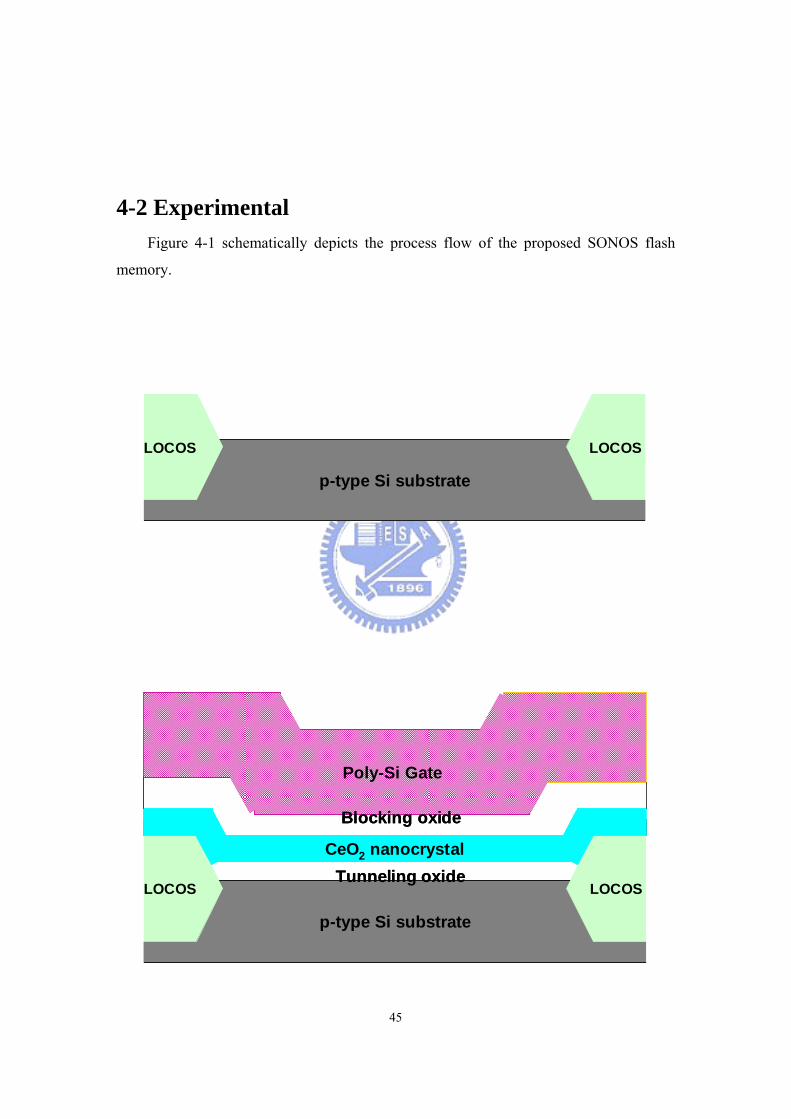
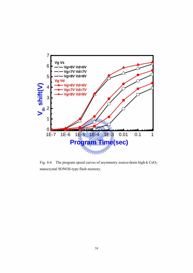
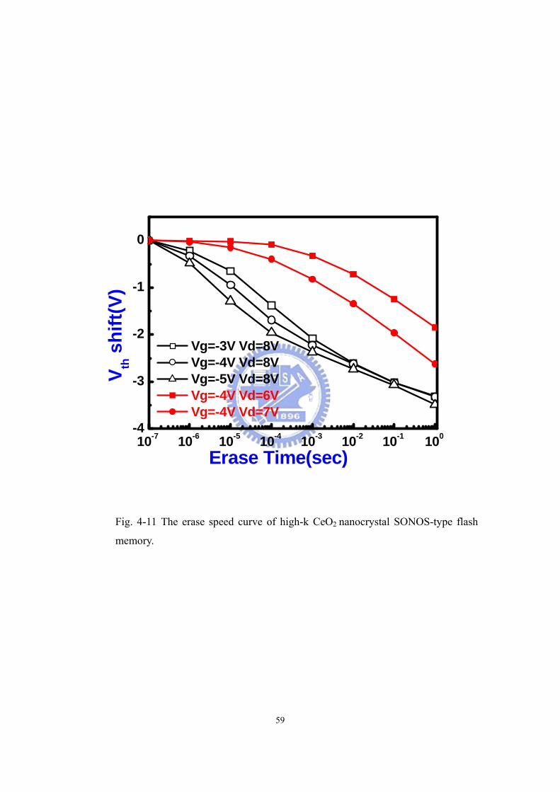