Embed Size (px)
Citation preview

1
The state-of-the-art in Semiconductor Reverse Engineering (RE101)
Randy Torrance21st May 2008
About UsThe What and Why of Reverse EngineeringProduct TeardownsSystem Analysis Process AnalysisCircuit AnalysisSchematic/Image viewing in
AgendaAgenda

2
ChipworksChipworks
Chipworks is a reverse engineering services company, based in Ottawa, Canada, with offices around the world providing semiconductor companies with:
Technical Intelligence to engineers and business unit managers to give you a technical view of your competition.
Patent Intelligence to IP groups and law firms providing technical intellectual property services to support licensing negotiations and patent portfolio development.
Reverse Engineering – What is it?Reverse Engineering – What is it?
In the semiconductor industry, reverse engineering (RE) can be:
Product Teardowns – what chips are usedSystem Analysis – how chips are usedProcess Analysis – how chips are built, and what are they made ofCircuit Analysis – how chips work

3
Reverse Engineering - Is it legal?Reverse Engineering - Is it legal?
Reverse Engineering is protected by the Semiconductor Chip Protection Act:
Title 17. Copy rightsChapter 9. Protection of Semiconductor Chip Products906. Limitations on exclusive rights; reverse engineering; first(a) Notwithstanding the provisions of section 905, it is not an infringement of
the exclusive rights of the owner of a mask for –(1) A person to reproduce the mask work solely for the purpose of
teaching, analyzing, or evaluating the concepts or techniques embodied in the mask work or the circuitry. Logic flow, or organization used in the mask work; or
(2) A person who performs the analysis or evaluation described in paragraph (1) to incorporate the results of such conduct in an original mask work which is made to be distributed
Why Reverse Engineer?Why Reverse Engineer?
To provide competitive technical intelligence (Or patent infringement intelligence.) Technical intelligence is uniquely fact-based and helps answer questions that fit neatly into the goals of several stakeholder groups.

4
Why Use Reverse Engineering to Reduce Design Cost?Why Use Reverse Engineering to Reduce Design Cost?
Average design costs are now ~$4M with a 12% CAGR in the last 5 years
Number of new designs decreased from just over 6000 to just under 5000 in the same time period.
Reverse engineering ensures that you meet or exceed your competitors devices and not just the specification
Reverse engineering is used successfully with 95% of the big semiconductor companies counted among Chipworks customers
Source: VLSI Research
The Start to Reverse Engineering
Product Teardown – example: Apple’s iPhone
The Start to Reverse Engineering
Product Teardown – example: Apple’s iPhone
Image © Chipworks Image © Chipworks
Image © Chipworks
Image © ChipworksImage © Chipworks

5
iPhone Product Teardown - iPod boardiPhone Product Teardown - iPod board
Image © Chipworks
Samsung 64-Gb dual-stack
package, multi-level cell NAND Flash memory (same as 8-GB
iPod)
Apple (NXP) power
manager
Apple/Samsung application
processor with ARM 1176 core + 1 Gb mobile DDR SDRAM memory,
package-on-package
configuration
Wolfson WM8758BG audio codec
(fabbed by TI)
STMicroelectronics LIS302D 3-
axis MEMS accelerometer
iPhone Product Teardown - Wireless boardiPhone Product Teardown - Wireless board
Image © Chipworks
Intel PF38F1030W0YTQ2 32 Mb NOR Flash +
16 Mb PSRAM
Infineon PMB8876 S-Gold2 baseband
processor
Marvell W8686B13WLAN
Skyworks SKY77340 power amplifier module
EDGE MCP including Peregrine
SP4T RF switch
Infineon GSM transceiver(?)
CSR 41B14BlueCore4-ROM

6
Hardware analysis:Reverse-engineering at the circuit or board levelFunctional analysis using test stimulus and monitoring outputs and internal signals
Software analysis:Software reverse engineering involves extraction and reconstruction of embedded codeSoftware functional analysis
= +
Types of System Analysis
Image © Chipworks
Intel PF38F1030W0YTQ2
32 Mb NOR Flash + 16 Mb PSRAM
Infineon PMB8876 S-Gold2 baseband
processor
Marvell W8686B13WLAN
Skyworks SKY77340 power amp module
EDGE MCP including Peregrine SP4T RF
switch
Infineon GSM transceiver
CSR 41B14BlueCore4-ROM
Teardown device─ Screwdrivers, etc
Identify components─ Datasheets, web, internal
part numbering mapsRemove componentsDelayer boards─ Delayering station
Trace connections─ IC Inside (our circuit
analysis software)Draw schematics─ IC Inside, Cadence
Composer
System Analysis - Hardware Reverse Engineering

7
For example: Discover how a digital camera works in order to prove use of invention
Examine patent...
…disassemble camera to get a dismembered but functioning camera...
System Analysis - Hardware Functional Analysis
…connect probesbetween the interfacesand a logic analyzer...
…create testbench and test vectors, test, collect
waveforms, study the timing...
…and document the evidence
System Analysis - Hardware Functional Analysis

8
Binary
Extract code…
System Analysis - Software Reverse Engineering
Assembler
‘C-like’ Code
Disassemble code…
Decompile code…
Process Analysis Process Analysis
Look at the structure of a chipIdentify the chemical make-up of the structureEstimate the process sequence
Capabilities

9
The “Rules” of Process RE The “Rules” of Process RE
We see what we see!We can’t see everything we want to seeSometimes we don’t know what we see!Sample preparation isn’t perfect – it can create confusing artifactsWhat we see doesn’t always agree with corporate marketing hypeSEM/TEM calibrations are NIST/NPL traceable and +/- 5% accurate
Extracted from Sony DCR-DVD505 Handycam
Process Analysis – Sony’s Clearvid IMX013 4-Mpixel CMOS Image SensorProcess Analysis – Sony’s Clearvid IMX013 4-Mpixel CMOS Image Sensor
Sensor module
Die photo

10
Process Analysis – IMX013 Pixel Array – Plan ViewProcess Analysis – IMX013 Pixel Array – Plan View
SEM images of organic & nitride lenses
Metal 3 Metal 2
Metal 1
Transistors
Process Analysis – IMX013 Pixel Array – Plan ViewProcess Analysis – IMX013 Pixel Array – Plan View
Substrate Doping

11
M1
Transfer transistor
SCM X-section
Nitride lens
Process Analysis – Cross-Section of Pixel ArrayProcess Analysis – Cross-Section of Pixel Array
-0.6
-0.5
-0.4
-0.3
-0.2
-0.1
0-1.4-1.2-1-0.8-0.6-0.4-0.20
VDS
I D (
mA
/µm
)
Nanoprober can probe transistors to 45-nm node (with great care!)Allows us to compare transistor performance against industry published data, competitive product, or previous generations
Transistor CharacterizationTransistor Characterization

12
Analog VS Embedded Memory, Standard Logic, I/O
Functional Analysis – Understand the ArchitectureFunctional Analysis – Understand the Architecture
Block Identification
NAND Cell
Functional Analysis – Cell Topology and LayoutFunctional Analysis – Cell Topology and Layout
6T SRAM
IO’s
Analog Blocks

13
Circuit RE FlowCircuit RE Flow
Die
Layers
Annotate Schematic
NetlistSimulate
Analysis, VerificationReports +
000XXXX
000XXXX
000XXXX
000XXXX00
0XXXX
000XXXX
000XXXX
000XXXX 00
0XXXX
000XXXX
000XXXX
000XXXX
000XXXX
000XXXX
000XXXX
000XXXX
000XXXX
000XXXX
000XXXX
000XXXX
000XXXX
000XXXX
000XXXX
000XXXX
000XXXX
000XXXX
000XXXX
000XXXX
000XXXX
000XXXX
000XXXX
000XXXX
000XXXX
000XXXX00
0XXXX
000XXXX
000XXXX
000XXXX
000XXXX
000XXXX00
0XXXX
000XXXX
000XXXX
000XXXX
000XXXX
000XXXX00
0XXXX
000XXXX
000XXXX
000XXXX
000XXXX
000XXXX
000XXXX
000XXXX
000XXXX
000XXXX
000XXXX
000XXXX
000XXXX
000XXXX
000XXXX
000XXXX
000XXXX
000XXXX
000XXXX
000XXXX
000XXXX
000XXXX
000XXXX
000XXXX
000XXXX
000XXXX
000XXXX
000XXXX
000XXXX
000XXXX
000XXXX
000XXXX
Delayering
Imaging
Stitching, Aligning
Annotation
Extraction, Analysis
Schematic Entry
NetlistSimulation
Verification
Depot
Reports
Circuit RE FlowCircuit RE Flow
14
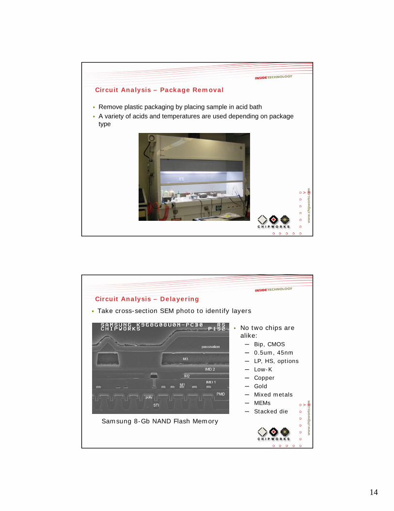
Remove plastic packaging by placing sample in acid bathA variety of acids and temperatures are used depending on package type
Circuit Analysis – Package Removal
Samsung 8-Gb NAND Flash Memory
Take cross-section SEM photo to identify layers
No two chips are alike:─ Bip, CMOS─ 0.5um, 45nm─ LP, HS, options─ Low-K─ Copper─ Gold─ Mixed metals─ MEMs─ Stacked die
Circuit Analysis – Delayering

15
An example:
Metals: Al, Cu, TiN, TaNMetal thickness: 0.15um to 1.4umDielectrics: silicon nitride, oxynitride, oxide, SiOC, SiONC, and PSGDielectric thicknesses: 47nm to 2.6µm
SEM cross-section of 65-nm TI baseband processor for Nokia
Delayering
Chose a technique and recipe, or develop a new oneRemove layers one by one, typically via:─ Reactive Ion Etching (RIE)─ Inductively Coupled Plasma (ICP)─ Polishing
Circuit Analysis – Delayering

16
• A sample is prepared for each metal interconnect layer, polysilicon layer and substrate diffusions.
• e.g. for 4 metal layer device, need to prepare 6 samples
Delayering
Atheros AR5110 - Metal 5 Atheros AR5110 - Metal 4
Delayering

17
Atheros AR5110 - Metal 3 Atheros AR5110 - Metal 2
Delayering
Atheros AR5110 - Metal 1 Atheros AR5110 - Poly
Delayering

18
Delayering
Imaging
Stitching, Aligning
Annotation
Extraction, Analysis
Schematic Entry
Netlist
Simulation
Verification
Depot
Reports
Circuit RE FlowCircuit RE Flow
Capture high magnification images using microscope (SEM and optical), automated stage and digital cameraUse software to stitch all the images together, and for inter-layer registration
Image Capture

19
Optical vs. SEM – e.g TI OMAP1310, 0.13µm process, transistor layer450nm optical light just doesn’t cut it anymore
Optical SEM
Image Capture
Delayering
Imaging
Stitching, Aligning
Annotation
Extraction, Analysis
Schematic Entry
Netlist
Simulation
Verification
Depot
Reports
Circuit RE FlowCircuit RE Flow

20
The olden days…
Annotation
The olden days…
Annotation

21
The olden days…
Annotation
AnnotationAnnotation
Metal-3
Metal-2
Metal-1
Annotations on eachimage layer
Correctinterlayer
registration
Fast, accuratecircuit
extraction
Software Automation•Wires are traced on the layer where they appear•Annotations are visible in any/all views•Lock-step cursors make layer changes easy to follow

22
Synchronized multi-layer display and annotation:
Patented lock-step cursors make layer
changes easy to follow
Wires are traced on the layer where they appear
Annotations visible in
any/all views
Annotation
Annotation – Polygon Feature Extraction
Raw M4 layer image

23
Edge Detection
Annotation – Polygon Feature Extraction
Fill in polygons based on heuristics (size, brightness, color, etc.)
Annotation – Polygon Feature Extraction

24
Circuit Analysis – Polygon Feature Extraction
Rule-based DRCs can improve accuracy
E.g. small breaks in wires, floating or missing contacts
Feature extraction challenges:Visibility of other layersBrightness variabilitySample prep artifacts
Further automation is possible after the feature recognition:
After wires are annotated vias can often be placed automaticallyOnce a device is defined, identical instances of this device can be searched for and found using pattern matching image recognition
This is especially useful for digital logic
Standard cell recognition
Annotation – Ever More Automation

25
Delayering
Imaging
Stitching, Aligning
Annotation
Extraction, Analysis
Schematic Entry
Netlist
Simulation
Verification
Depot
Reports
Circuit RE FlowCircuit RE Flow
Two methods are available for moving from annotated images to schematics or netlist:
Manual extractionUsed by experienced analysts for sub-circuits where the schematic is quickly visible from the imagesCan be a very efficient method of simultaneous circuit extraction and analysis, since the schematic can be organized as it is drawn.
Automated extraction Very useful for large blocks of circuitry, and is especially valuable for digital blocks.Devices are placed in schematic in the same locations they occupy in the layout Becoming the norm, since it creates a schematic “correct by design”
Schematic Readback

26
Auto-extracted devices placed relative to layout positions
A random arrangement of transistors or gates does not convey a great deal of information
Schematic Readback
3.0.0 Address Buffers IBM 165800CT5ADevice Type:
SIEMENS IBM BTV - B18
Date Code:
G:\MARKET\..\3-0-0ADP.SCHFile:
25-Sep-1998 11:52:13
Reference: ref.
Revision: 0 - AE
Die Markings: 8Mx8 CMOS DRAM
P28004WM PQOBERON 1994 DD2NP
Note: Device sizes are in microns (as measured from photographs) +/- 0.25 µm
ABEN_
[ A[0:12] ]
A[0:12]_A12BEN_A12PD
3.1.0 Address Input Buffers3-1-0AIB.SCH
ABEN_
[ A[0:12] ]
A[0:12]_A12BEN_A12PD
XA12
HCLCK
A[0:12]_
HASEL
A12BEN
RR8K/4K_AXQ12BA/_AXQ12BB/_AXQ12BC/_
AXQ[0:11]/_
RAS4T32
3.2.0 Row Address Buffers3-2-0RAP.SCH
XA12
HCLCK
A[0:12]_
HASEL
A12BEN
RR8K/4K_AXQ12BA/_AXQ12BB/_AXQ12BC/_
AXQ[0:11]/_
RAS4T32
AY[2:9]
MSX1MSX4MSX8MSX16
ZABENCABEN
TCBRTSTCLK
TMBRTOBE_
RR8K/4K_
WE
A[0:12]_XA12
AZ0AZTD0
AZ5/_AZ34P[0:3]
AZ[3:4]/_
AZ1/_AZ2/_
AYD[2:9]_
AZ5B/_
3.3.0 Column Address Buffers3-3-0CAP.SCH
AY[2:9]
MSX1MSX4MSX8MSX16
ZABENCABEN
TCBRTSTCLK
TMBRTOBE_
RR8K/4K_
WE
A[0:12]_XA12
AZ0AZTD0
AZ5/_AZ34P[0:3]
AZ[3:4]/_
AZ1/_AZ2/_
AYD[2:9]_
AZ5B/_
TABEN_
INTA1_
CABENTABEN
INTA_
INTASEL
TXAB/_
TYA_
TYA
[P68]
3.4.0 Test Address Buffers3-4-0TAP.SCH
TABEN_
INTA1_
CABENTABEN
INTA_
INTASEL
TXAB/_
TYA_
TYA
[P68]
HCLCK
[A[0:12]]
HASEL
A12BEN
RR8K/4K_AXQ12BA/_AXQ12BB/_AXQ12BC/_
AXQ[0:11]/_
AY[2:9]
MSX1MSX4MSX8MSX16
ZABENCABEN
TCBRTSTCLK
TMBRTOBE_
WE
ABEN_
A12PD
AZ0AZTD0
AZ5/_AZ34P[0:3]AZ[3:4]/_
AZ1/_AZ2/_
AYD[2:9]_
AZ5B/_
A12BEN_
TABEN_
INTA1_
TABEN
INTA_
INTASEL
TXAB/_
TYA_
TYA
[P68]CABEN
RRTDEN[0:7]AXQ[5:7]/_
RRTAEN[0:3]_
3.5.0 Octant Test Decoder3-5-0OCT.SCH
RRTDEN[0:7]AXQ[5:7]/_
RRTAEN[0:3]_RRTAEN[0:3]_
RRTDEN[0:7]AXQ[5:7]/_
RAS4T32
RR8K/4K_
3.2.1 Primary Row Address BuffersIBM 165800CT5ADevice Type:
SIEMENS IBM BTV - B18
Date Code:
G:\MARKET\..\3-2-1RAB.SCHFile:
25-Sep-1998 12:12:42
Reference: ref.
Revision: 0 - HK
Die Markings: 8Mx8 CMOS DRAM
P28004WM PQOBERON 1994 DD2NP
Note: Device sizes are in microns (as measured from photographs) +/- 0.25 µm
10/.5
5/.5
2/.5
VCC
10/.5
5/.5
2/.5
VCC
5/.5
2/.5
10/.5, 3.2/.5
20/.5, 10/.5
6/.5
3/.5
6/.5
3/.5
A[0:11]_
HA[0:11]
2.2/.5
2.2/1
2.2/.5
2.2/.510/.5
12/.5 4/.5
VCC VCC
10/.52.2/.5
4/.5 12/.5
VCC VCC
40/.5
10/.5
40/.5
10/.5
99/.5
82/.5
4/.5
2/.5
4/.5
2/.5
99/.5
82/.5
4/.5
8/.5
AXH[0:11]/_
4/.5
2.2/.5
HASEL
8/.5
3/.5
RAS4
HASEL
HASEL
pc_
pc_
AXH[0:11]_
AXH[0:11]
pc_
JA96
14/0.5
14/0.5
13/0.5
106/0.5
36/0.5
T32
RAS4
A0, A1, A2, A8, A9, A10, A11
A3, A4, A5, A6, A7
pc_
(1 of 12)
pc_
pc_ = RAS4 for
pc_ = RAS4g forGB38
JA72
RAS4g
GB35_
The analysis phase:arranging the transistors and gatesorganizing a readable, hierarchical schematic setunderstanding the function and reason behind the design
Analysis

27
ToolsSchematic organization can be done using the usual design schematic editors (e.g. Cadence Composer)However, these tools tend to be optimized for forward design rather than reverse engineeringA specialized RE schematic editor is optimized for schematic organization from layout
Simple structures such as diff pairs and current mirrors can be found automaticallySubcircuits are easily grouped, created, and linked hierarchicallySubcircuit input devices can all be gathered with one keystrokeIdentical subcircuits can be located and organized automatically
Analysis
Example sub-circuit search and organization
Analysis
Auto-extracted devices placed as per the layout to give a flat, unorganized schematicOne instance of a sub-circuit defined manually, others matched and organized automaticallyCan place in sub-cells

28
Re-creating meaningPublic information and datasheets can help with schematic organizationTechnical papers from journals and conferences hold interesting clues
IEEE ExploreFloorplan and layout information can be very valuable
For analog circuits the layout often follows a logical progressionFor digital… not so much
An experienced RE analyst is invaluable.
Analysis
Delayering
Imaging
Stitching, Aligning
Annotation
Extraction, Analysis
Schematic Entry
Netlist
Simulation
Verification
Depot
Reports
Circuit RE FlowCircuit RE Flow

29
As with forward design, the first pass schematic is not always 100% correctHowever, in contrast to forward design, 100% correct is normally less essential:
Clients are usually most interested in circuit structureDevice sizes only need to be approximate
Even if simulation is desired, we rarely have process models for competitive chips, and hence accurate device sizes are not critical
Of course, device sizes can only be accurate as measured from actual devices:
As measured on silicon, not mask sizes or layout database sizesThe process on any particular device could be anywhere between best and worst case
Verification
Multiple techniques are available:Redundant annotation, netlist compareGreater use of automated extraction toolsOur schematic editor flags errors whenever the connectivity is broken (connectivity derived from annotated images)Simulation (either digital or analog)MicroprobingAnd, of course, experienced analysts who can quickly see when a circuit makes sense, and when it doesn’t
Capture Schematics
Generate Netlist Set Up Analyses
Simulate
Analyze ResultsReview Schematics based on Sim results
Schematic Editor Spice
Verification

30
Delayering
Imaging
Stitching, Aligning
Annotation
Extraction, Analysis
Schematic Entry
Netlist
Simulation
Verification
Depot
Reports
Circuit RE FlowCircuit RE Flow
3.0.0 Address BuffersIBM 165800CT5ADevice Type:
SIEMENS IBM BTV - B18
Date Code:
G:\MARKET\..\3-0-0ADP.SCHFile:
25-Sep-1998 11:52:13
Reference: ref.
Revision: 0 - AE
Die Markings: 8Mx8 CMOS DRAM
P28004WM PQOBERON 1994 DD2NP
Note: Device sizes are in microns (as measured from photographs) +/- 0.25 µm
ABEN_
[ A[0:12] ]
A[0:12]_A12BEN_A12PD
3.1.0 Address Input Buffers3-1-0AIB.SCH
ABEN_
[ A[0:12] ]
A[0:12]_A12BEN_A12PD
XA12
HCLCK
A[0:12]_
HASEL
A12BEN
RR8K/4K_AXQ12BA/_AXQ12BB/_AXQ12BC/_
AXQ[0:11]/_
RAS4T32
3.2.0 Row Address Buffers3-2-0RAP.SCH
XA12
HCLCK
A[0:12]_
HASEL
A12BEN
RR8K/4K_AXQ12BA/_AXQ12BB/_AXQ12BC/_
AXQ[0:11]/_
RAS4T32
AY[2:9]
MSX1MSX4MSX8MSX16
ZABENCABEN
TCBRTSTCLK
TMBRTOBE_
RR8K/4K_
WE
A[0:12]_XA12
AZ0AZTD0
AZ5/_AZ34P[0:3]
AZ[3:4]/_
AZ1/_AZ2/_
AYD[2:9]_
AZ5B/_
3.3.0 Column Address Buffers3-3-0CAP.SCH
AY[2:9]
MSX1MSX4MSX8MSX16
ZABENCABEN
TCBRTSTCLK
TMBRTOBE_
RR8K/4K_
WE
A[0:12]_XA12
AZ0AZTD0
AZ5/_AZ34P[0:3]
AZ[3:4]/_
AZ1/_AZ2/_
AYD[2:9]_
AZ5B/_
TABEN_
INTA1_
CABENTABEN
INTA_
INTASEL
TXAB/_
TYA_
TYA
[P68]
3.4.0 Test Address Buffers3-4-0TAP.SCH
TABEN_
INTA1_
CABENTABEN
INTA_
INTASEL
TXAB/_
TYA_
TYA
[P68]
HCLCK
[A[0:12]]
HASEL
A12BEN
RR8K/4K_AXQ12BA/_AXQ12BB/_AXQ12BC/_
AXQ[0:11]/_
AY[2:9]
MSX1MSX4MSX8MSX16
ZABENCABEN
TCBRTSTCLK
TMBRTOBE_
WE
ABEN_
A12PD
AZ0AZTD0
AZ5/_AZ34P[0:3]AZ[3:4]/_
AZ1/_AZ2/_
AYD[2:9]_
AZ5B/_
A12BEN_
TABEN_
INTA1_
TABEN
INTA_
INTASEL
TXAB/_
TYA_
TYA
[P68]
CABEN
RRTDEN[0:7]AXQ[5:7]/_
RRTAEN[0:3]_
3.5.0 Octant Test Decoder3-5-0OCT.SCH
RRTDEN[0:7]AXQ[5:7]/_
RRTAEN[0:3]_RRTAEN[0:3]_
RRTDEN[0:7]AXQ[5:7]/_
RAS4T32
RR8K/4K_
3.2.1 Primary Row Address BuffersIBM 165800CT5ADevice Type:
SIEMENS IBM BTV - B18
Date Code:
G:\MARKET\..\3-2-1RAB.SCHFile:
25-Sep-1998 12:12:42
Reference: ref.
Revision: 0 - HK
Die Markings: 8Mx8 CMOS DRAM
P28004WM PQOBERON 1994 DD2NP
Note: Device sizes are in microns (as measured from photographs) +/- 0.25 µm
10/.5
5/.5
2/.5
VCC
10/.5
5/.5
2/.5
VCC
5/.5
2/.5
10/.5, 3.2/.5
20/.5, 10/.5
6/.5
3/.5
6/.5
3/.5
A[0:11]_
HA[0:11]
2.2/.5
2.2/1
2.2/.5
2.2/.510/.5
12/.5 4/.5
VCC VCC
10/.52.2/.5
4/.5 12/.5
VCC VCC
40/.5
10/.5
40/.5
10/.5
99/.5
82/.5
4/.5
2/.5
4/.5
2/.5
99/.5
82/.5
4/.5
8/.5
AXH[0:11]/_
4/.5
2.2/.5
HASEL
8/.5
3/.5
RAS4
HASEL
HASEL
pc_
pc_
AXH[0:11]_
AXH[0:11]
pc_
JA96
14/0.5
14/0.5
13/0.5
106/0.5
36/0.5
T32
RAS4
A0, A1, A2, A8, A9, A10, A11
A3, A4, A5, A6, A7
pc_
(1 of 12)
pc_
pc_ = RAS4 for
pc_ = RAS4g forGB38
JA72
RAS4g
GB35_
Organized, readable, hierarchical schematics
Optional Outputs: Netlists, simulated waveforms,micro-probed waveforms, block diagrams, timing diagrams, circuit equations
Circuit Analysis - DeliverableCircuit Analysis - Deliverable
31
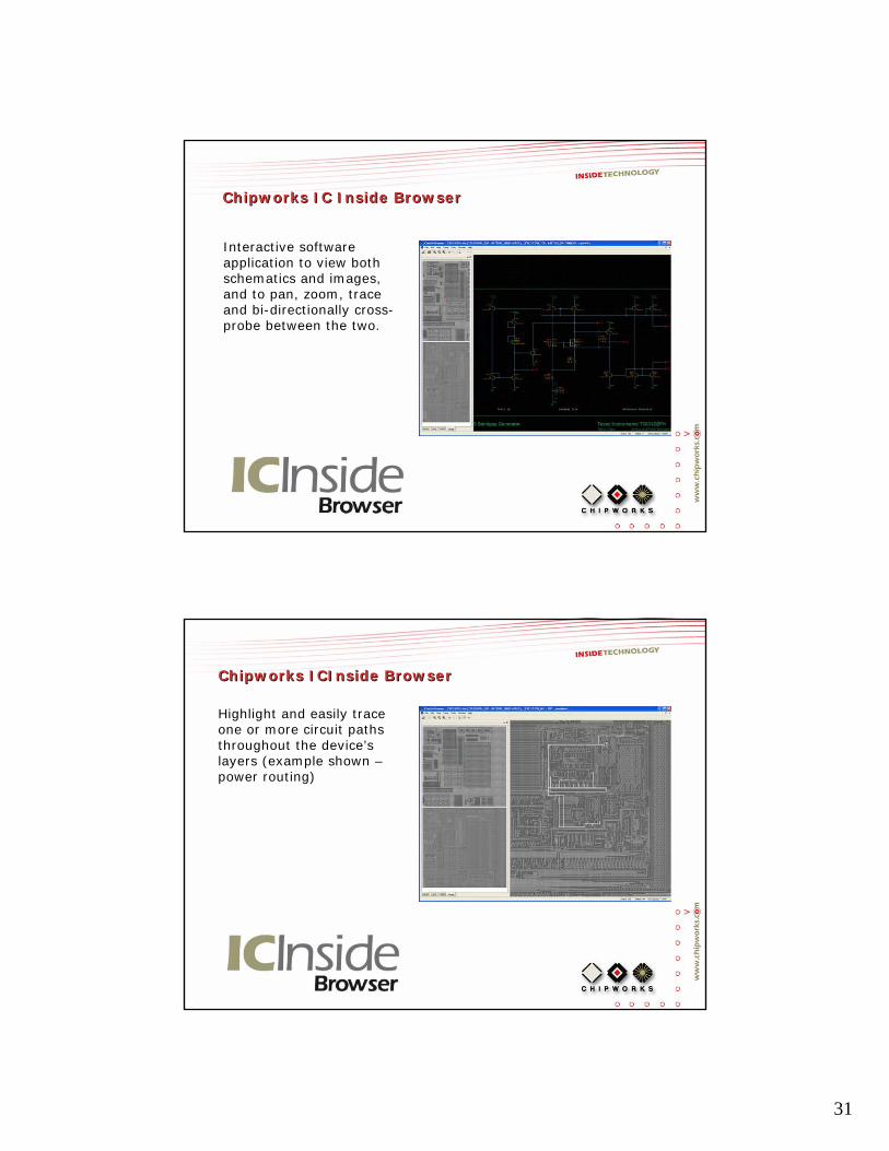
Chipworks IC Inside BrowserChipworks IC Inside Browser
Interactive software application to view both schematics and images, and to pan, zoom, trace and bi-directionally cross-probe between the two.
Chipworks ICInside BrowserChipworks ICInside Browser
Highlight and easily trace one or more circuit paths throughout the device’s layers (example shown –power routing)

32
Powerful Export CapabilityPowerful Export Capability
Schematic Editors (EDIF200)
Netlist
Simulate
ICInside Browser
SummarySummary
I have reviewed the reverse engineering of electronic systems, circuits, and component structures.RE of semiconductors requires state-of-the-art, leading-edge equipment.It is possible to extract operational and manufacturing information as well as system, circuit, and process.This provides intelligence for product/process development, marketing, and bench-marking.It can also be correlated with patents and other IP to show evidence of IP usage.

33
I would like to thank Chipworks’ laboratory staff and analysts, who actually do all the hard work of analyzing these complex devices. They do a great job!
AcknowledgementAcknowledgement
If I have seen further it is only by standing on the shoulders of giants.
-Isaac Newton
Chipworks can help you meet your competitive intelligence needs