Embed Size (px)
Citation preview

1
THE SAFE OPERATING AREA (SOA) PROTECTION OF LINEAR AUDIO
POWER AMPLIFIERS
Michael Kiwanuka, B.Sc. (Hons) Electronic Engineering.
Introduction
The desirability, or lack thereof, of over-voltage and over-current protection for power
semiconductors in audio power amplifiers remains a point of contention in the field 1 . For example,
some designers 2 appear to recommend multiple-transistor complementary output stages, as often
mandated by high-power class-A operation, to circumvent the need for SOA protection of bipolar
devices, while others 3 suggest that such voltage-current (alias V-I) limiters may be dispensed with
altogether by merely adopting enhancement-mode power MOSFETs (hereinafter e-MOSFET).
These views appear to be rather more widely accepted than they should, and constitute a charter for
near heroic unreliability in amplifiers so designed, as even a momentary short to ground can destroy
an expensive output stage. The zener diode-clamping of the gate-source voltage of e-MOSFETs is
thought by some 54, to be all that is required in regard to protection. While the zener diodes are
mandatory (ideally with VVV zener 2010 << to prevent premature clamping) they only serve to
protect the e-MOSFET’s gate oxide insulation from over-voltage destruction 6 , and do nothing
whatever to protect the device from accidental short circuits and forbidden voltage-current
combinations that may occur when the amplifier is called upon to drive reactive loads.
The positive temperature coefficient of on-resistance 7 (and therefore negative temperature
coefficient of drain current) enjoyed by e-MOSFETs eliminates the secondary breakdown
phenomenon which is the bane of bipolar transistors, but does not constitute licence for wilful
violation of power dissipation limits in linear audio-frequency applications. This is in contrast to
ultrasonic switching usage, where e-MOSFET dissipation bounds may be blissfully ignored, and
adherence to drain current and drain-source voltage limits will suffice.
All output stage semiconductors used in complementary or quasi-complementary (full or half bridge)
linear audio power amplifiers, without exception, require SOA protection for reliable operation.
However, such circuitry must be carefully designed to prevent premature activation during normal
amplifier operation.
Single slope linear foldback limiting
Many low to medium-power (sub-200W into 8Ω) commercial audio amplifiers incorporate a single
slope linear foldback voltage-current protection circuit (fig. 1) attributed to S.G.S. Fairchild Ltd. by
Dr A.R. Bailey 8 . In practice, the complimentary output transistors 1OT and 2OT may each consist of
a compound arrangement of at least two transistors in series.
The instantaneous collector-emitter voltage cev across 1OT is sensed by R1, R2 and R3, while the
output current, expressed as a voltage across emitter resistor eR , is simultaneously monitored by R2
and R3. Thus these voltages are summed algebraically at the base of protection transistor 1PT which
is driven into conduction shunting voltage drive to 1OT in the event of an over-voltage, over-current
or simultaneous occurrence of both conditions in the output device.

2
Fig. 1. Improved version of Fairchild’s single slope linear foldback protection circuit applied to a complementary
output stage.

3
The series resistor SR (typically 2K2RR100 S ≤≤≤≤≤≤≤≤ ) expedites this process by limiting the current
required by 1PT to shunt voltage drive to 1OT . The freewheeling diode FD protects the output device
from excessive base-emitter reverse bias 9 , due to beyond-rail voltage spikes generated when SOA
protection is invoked with inductive loads, while PD performs the same function for the small-signal
protection transistor 1PT by preventing its base-collector junction from being forward biased 5 .
If the amplifier’s output approaches the negative supply rail while driving a sufficiently low
impedance, the current sunk by 2OT generates an appreciable voltage drop across its emitter resistor *
eR ; the output is then at an appreciably higher potential than the common input to the
complementary output stage. Consequently, transistor 1OT is reverse biased and s'TP1 base-collector
junction, in the absence of its collector diode PD , would be forward biased causing current to flow
from emitter to collector.
Diode PD prevents this form of spurious inverse-active mode limiter activation by decoupling s'T 1P
collector as s'T 1O base-emitter junction is reverse biased. The potential at s'T 1O emitter is then
equal to the output voltage since 1OT is non-conducting and, contrary to Duncan 10 , only negligible
leakage current flows through its emitter resistor eR . By symmetry the explanation above also
applies to the negative half of the circuit.
A small-value capacitor is sometimes connected across the base-collector junction of each protection
transistor1 with a view to eliminating oscillation that occurs in the network during the limiting
process. These capacitors appear in parallel at AC and are entirely unsatisfactory, as they create an
ill-defined and therefore undesirable feedfoward path around the output stage, shunting it out of the
global feedback loop at high audio frequencies-precisely where the amplifier is most vulnerable with
respect to non-linearity.
Such vulnerability is due to a necessarily diminished feedback factor at high audio frequencies in the
interest of Nyquist stability. Connecting the capacitor across the base-emitter junction of each
protection transistor is the preferred solution.
Series base resistors bR and *
bR (of the order of 10K) are also recommended for each protection
transistor. These base ballast resistors make for better controlled activation of the protection
transistors by damping anomalous voltage spikes otherwise provoked by these transistors being
overdriven.
Additionally, the single pole low-pass filters comprising ballast resistors bR , *
bR and shunt
capacitors SC , *
SC prevent activation of the protection transistors at ultra-sonic frequencies where
such protection is unnecessary. For typical values, the source impedance of the protection circuit
(referred to the base of each protection BJT) may be deemed negligible compared to the value of the
ballast resistor. For brevity, diodes FD , ∗FD , PD , ∗
PD , base-emitter shunt capacitors SC , *
SC and
ballast resistors bR , *
bR are omitted in all subsequent figures.
The values of bR and SC shown in figure 1 provide 6dB of attenuation at approximately 1Khz. This
is roughly equivalent to doubling the permissible power dissipation per output device at this
frequency.

4
The filter’s nominal time constant may not exceed 500µS with bipolar output transistors, as the filter
is required to partially damp the oscillation that occurs during limiting and not completely eliminate
it. This is because this oscillation is intrinsic to the circuit’s operation.
For instance, if the amplifier’s output swings positive during persistent SOA overload (such as a
continuous short-circuit to ground or negative supply rail), protection transistor 1PT is driven
forward-active, cutting off output transistor 1OT . The fault is therefore removed with respect to 1OT
and protection transistor 1PT is promptly disabled. This in turn causes the instantaneous recurrence
of the overload condition and attendant reactivation of 1PT . The on-off action of the protection
transistor in these circumstances appears as persistent local high frequency oscillation which,
contrary to popular opinion, has nothing to do with the stability of the protection circuit or, indeed,
the amplifier’s major feedback loop.
The resistor values for the arrangement of figure 1 are obtained by drawing the desired protection
locus on a linear-linear scale graph of the output transistor’s DC safe operating area (fig. 2). One of
the three resistors (usually R3) is assigned an arbitrary value (typically K13RR100 ≤≤≤≤≤≤≤≤ ), and the
two remaining resistors evaluated from simultaneous equations developed from two convenient
points on the protection locus.
Fig. 2. Safe operating area of On Semiconductor®’s MJL3281A; the single slope linear foldback protection locus
is drawn to intersect the Vce-axis at a value greater than ccV2 to prevent premature limiting.
5
With this arrangement, it is essential that the linear protection locus intersect the SOA’s Vce axis at a
value greater than the sum of the moduli of the amplifier’s voltage supplies; otherwise 1PT turns on
under normal loading when the output swings negative, even with the output open-circuit. Similarly,
2PT would be activated under normal output loading when the output swings positive. This
effectively short-circuits the “small signal” circuit preceding the output stage directly to the output,
causing gross distortion.
Failure to adhere to the above condition appears to have caused some designers to erroneously
abandon electronic SOA protection of any form altogether 121, . However, this requirement presents a
significant impediment to the efficient utilisation of the comparatively large SOA in the low-Vce
region of the graph. This is especially true of amplifiers with relatively high supply-rail voltages
where in the case of bipolar transistors secondary-breakdown severely curtails flexibility in optimal
placement of the protection locus.
This is graphically illustrated in figure 2 for an amplifier with nominal ±40V supply rails, and using
On Semiconductor®’s excellent 13 200W MJL3281A-MJL1302A complementary power
transistors. Note that although the datasheet SOA of 200W for these devices is used here for brevity,
this is specified at a device case temperature CTo
C 25= . The later is only achievable with an
improbable heat sink of infinite dimensions. In practice, the datasheet SOA should be adjusted (viz.
“derated”) to accommodate the transistor’s steady state case temperature with the designer’s selected
heat sink.
Only the positive half of the circuit of figure 1 need be used to calculate the required passive
component values (fig. 3). Ideal active devices are assumed, with infinite input impedance, zero
saturation voltage and zero ohmic resistance. The error thus accrued is negligible, provided small-
signal transistors of high current-gain ( )100≥β are used. Let beV =0V6, 3R =220R and Re=0R22.
Taking two arbitrary points A and B on the locus where at point A Ic=6.85A, Vce=0V, and at point
B Ic=4A, Vce=36V, it follows from figure 3:
( )220220
507160
112
2
++=
RRR
R.. (1)
With reference to figure 4 and noting that the contribution of 3
I to the current in e
R is negligible:
312 III += (2)
⇒
( ) ( ) 312 72347234060 R.R.R. −+−=
⇒
( )220280283660 12 .R.R. += (3)
Solving (1) and (3) simultaneously gives 1R ≈≈≈≈ 12K4 and 2R ≈≈≈≈ 143R0. For enhanced accuracy it is
recommended that these values be made up from series or parallel combinations of 1% resistors
where necessary.

6
When the output swings to -40V, then 80V appears across 1R in series with 32 R//R to a good first
approximation. Thus, the voltage present at the base of the protection transistor 1PT is given by:
55080
132
32 VR)R//R(
)R//R(Vbe ≈
+≈
Therefore, it follows that spurious activation of 1PT cannot occur if instantaneous collector current
ci is less than the maximum permissible collector current I )MAX(C at ccce Vv 2≈ . A general
expression that facilitates the rapid verification of the compliance of any amplifier using single slope
linear foldback limiting may be developed:
( )
( ) becc V
RR//R
R//RV<
+ 132
322
⇒
(((( ))))
2 3
2 3 1 2 1 3 25
20 6
oA
cc
T C
V R RV
R R R R R R====
<<<<+ ++ ++ ++ +
(4)
Equation 4 is true only at an ambient temperature A
T of 25oC as the threshold voltage of the
protection transistors may be expected to drop roughly 2mV per degree Celsius increase in
temperature. Further equation 4 is valid subject to the following condition:
ccce VvMAXCC Ii
2≈< )( (5)
This condition is invariably fulfilled during normal operation, as no practical loudspeaker system
would demand that the output transistor sustain ccce Vv 2≈ while providing any appreciable current.

7
Fig. 3. Output conditions at point A on the protection locus of figure 2.

8
Fig. 4. Output conditions at point B on the protection locus of figure 2. The contribution of 3
I to the current in Re
is negligible.

9
Figure 5 shows a common variation 10 11 13 14, , , on the single slope linear foldback limiter of figure 1,
with resistor 2R excised so that from equation 4:
( )
602
23113
3 VR/RRRR
RVcc <++
Since ∞→2R , then:
(((( ))))
3
3 1 25
20 6
oA
cc
T C
V RV
R R====
<<<<++++
The optimal protection locus for this network (fig. 6) must be plotted so that calculated resistor
values comply with the above condition. This scheme is atrociously inefficient, as for a nominal
VVce 0≈ and Re=0R22, resistors 1R and 3R are in parallel and, of necessity, the collector current
ci is prematurely limited to ( ) 720
ARVI ebeVVcce
≈<≈
.
A value of Re=0R1 gives a modest improvement, with ( ) 060
ARVI ebeVVcce
≈<≈
. Clearly claims 13
of “load-invariant” drive capability made for power amplifiers using this scheme are rather
premature.
The protection locus is realised by deriving output stage conditions (fig. 7) at a single arbitrary point
B on the locus subject to ccce VV 20 << . With VVcc 40= , Re = 0R22, 3R =220R and noting that
1R and 3R constitute a simple voltage divider, then:
( )
( )K
R..
.R 46
2207839439
439401 ≈
+−
+≈
This unwarranted dependence on the value of Re is unacceptable as in some applications, such as
output stages comprising paralleled complementary e-MOSFET pairs, )RRR( e 0110 ≤< may be
required to guarantee equable current sharing.

10
Fig. 5. Compromised single slope linear foldback scheme gives grossly inefficient SOA utilisation.

11
Fig. 6. Linear protection locus clearly shows the inflexibility of the scheme of figure 5.

12
Fig. 7. Output conditions at point B on the protection locus of figure 6.
13
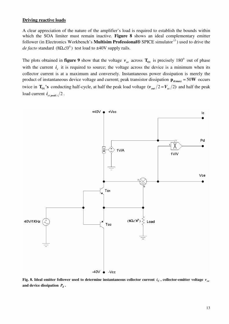
Driving reactive loads
A clear appreciation of the nature of the amplifier’s load is required to establish the bounds within
which the SOA limiter must remain inactive. Figure 8 shows an ideal complementary emitter
follower (in Electronics Workbench’s Multisim Professional® SPICE simulator15 ) used to drive the
de facto standard )08( 0∠Ω test load to ±40V supply rails.
The plots obtained in figure 9 show that the voltage cev across 1OT is precisely 0180 out of phase
with the current ci it is required to source; the voltage across the device is a minimum when its
collector current is at a maximum and conversely. Instantaneous power dissipation is merely the
product of instantaneous device voltage and current; peak transistor dissipation Wp (max)d 50≈ occurs
twice in s'TO1 conducting half-cycle, at half the peak load voltage )( 22 ccout Vv ≈ and half the peak
load current 2)( peakci .
Fig. 8. Ideal emitter follower used to determine instantaneous collector current Ci , collector-emitter voltage cev
and device dissipation dP .

14
Fig. 9. Instantaneous cev , Ci and dP in sourcing output transistor while driving roughly 39V across an )08( 0∠∠∠∠ΩΩΩΩ
load.
Since the )08( 0∠Ω load line resides well below the linear protection locus of figure 10 (reproduced
from fig. 2), it is clear that a single pair of MJL3281A-MJL1302A power transistors operating from
±40V rails will comfortably drive an 8Ω dummy load to clipping without invoking protection;
however, this will certainly not be the case with loudspeaker loads, which are invariably reactive 17,16 .
An amplifier with “high-fidelity” aspirations, intended to drive full-range multiple-transducer
loudspeaker systems, including electrostatics, should at least be capable of driving a (4Ω ∠ ± 60 0 )
impedance without invoking SOA-protection.
A (4Ω ∠ -60 0 ) impedance was devised in SPICE by driving a 2Ω0 resistor in series with a 45µ9441
capacitor at 1Khz with the ideal complementary emitter follower of figure 8. The traces thus
obtained (fig. 11) were used to plot the )604( 0±∠Ω load line in figure 10. Peak transistor
dissipation Wp (max)d 362≈ (with ~ ( )PeakV39 across the load) occurs at Vvce 946.≈ and .A.ic 77≈
In other words (fig. 12), because current leads voltage in a capacitive impedance, transistor 1OT (fig.
8) is required to source Aic 77.≈ when the output swings away from the negative supply rail to
.Vvout 6−≈ Similarly, transistor 2OT must sink Aic 77.≈ when the output swings from +Vcc to
.Vvout 6+≈ Note that the crossover discontinuity in the output voltage characteristic (at Vvout 35≈ )
now precedes zero voltage crossing by 060 (fig. 12); this is contrary to the popular view that the
crossover discontinuity is coincident with zero voltage crossing regardless of the nature of the load.
With a )604( 0+∠Ω inductive impedance, in which current lags voltage, the output conditions are
reversed, with the load demanding Aic 77.≈ from 1OT when the output swings from the positive
supply to .Vvout 6−≈ Regardless of the nature of the load, however, device voltage cev and load
voltage outv are always 0180 out of phase and of course, being a voltage follower, the input voltage
is always in phase with outv at the frequencies of interest.

15
Fig. 10. The reactive load gives an elliptical characteristic which causes more than seven times greater peak device
dissipation than for the )08( 0∠∠∠∠ΩΩΩΩ case.
Fig. 11. Instantaneous cev , Ci and dP in sourcing output transistor 1OT obtained by driving a )604( 0−−−−∠∠∠∠ΩΩΩΩ load
to a little under (((( ))))PeakV40 .

16
The linear foldback protection locus (fig. 10) only permits 3A at Vce=46.9V; therefore a minimum
of three output pairs are required to drive a notional (4Ω ∠ ± 60 0 ) loudspeaker system from ± 40V
supply rails without intrusive limiter activation. Note that this may need to be “derated” to four
transistor pairs to accommodate realistic device case temperatures. On this basis, and using other
established techniques 18,11 , including mandatory DC offset and thermal overload protection systems,
a reliable and versatile low distortion amplifier may be constructed.
As the cost of power transistors is significant, there is a compelling financial incentive to minimise
the number of devices used by utilising the SOA as efficiently as possible. To this end, it has been
suggested 10 that, ideally, the protection locus should closely match the bounds of the SOA. This is
unnecessary, as reactive load drive primarily requires that current delivery in the cccecc VvV 2<≤
region be maximized without violating suitably derated DC safe operating limits. In general, as shall
be demonstrated, an optimally located nonlinear protection locus with at least one breakpoint should
suffice.
Fig. 12. Transistor 1OT delivers 7.7A to the )604( 0−−−−∠∠∠∠ΩΩΩΩ load when the output voltage swings away from -Vcc to -
6V. The crossover discontinuity marked X now precedes zero voltage crossing by 060 .

17
Single slope single breakpoint non-linear foldback limiting
Introducing a zero-gradient segment at some optimal point in the protection locus permits an increase
in current delivery at the low-Vce end of the SOA without significantly compromising available
current at higher device voltages (fig. 13). The single slope linear foldback protocol (equation 4) is
made redundant as the protection locus does not cross the Vce-axis at any point.
The zero-slope segment BC is realised by splitting 1
R in figure 1 into 1A
R , 1B
R and clamping the
voltage across 1B
R and 2
R with zener diode 1D (fig. 14) when 64 2 80≤ < =≤ < =≤ < =≤ < =ce cc V v ( V V) . When
)( VvV ce 640 <≤ , segment AB, the diode is off (virtually open-circuit) and the circuit reverts to a
single slope linear foldback regime. This scheme was apparently introduced by Ruehs 20 , but the
algebra used to establish component values was incorrect.
Fig.13. Single slope single breakpoint non-linear foldback protection locus.

18
The zener diode is disconnected and resistors 1A
R and 1B
R amalgamated into one resistor 1
R (fig.
15). As was the case with the circuit of figure 1, component values are then established for the
single-slope locus ABD at arbitrarily selected points A and B where at point A, Ic=7.5A, Vce=0V,
and at point B, Ic=1.5A, Vce=64V.
With reference to figure 15 and selecting 1R =100R:
(((( ))))
2
2 1 1
1 650 6
100 100
. R.
R R R====
+ ++ ++ ++ + (6)
From figure 16 and noting that the contribution of 3
I to the current in e
R is negligible:
2 1 3
I I I= −= −= −= −
⇒
(((( )))) (((( ))))2 1 30 6 40 23 73 23 73 24. R . R . R= + − − += + − − += + − − += + − − +
⇒
(((( ))))2 10 6 63 73 0 27 100. R . R .= −= −= −= − (7)
Solving (6) and (7) simultaneously gives 1R ≈≈≈≈ 4K8 and 2R ≈≈≈≈ 56R.
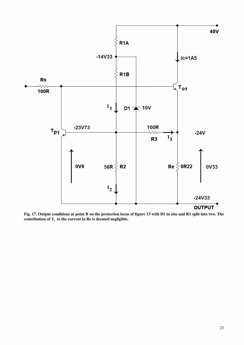
The zener diode, with an arbitrarily selected zener voltage 10Z
V V==== , is now introduced and resistor
1R split into resistors 1A
R and 1B
R (fig. 17). At point B in the protection locus of figure 13 the
diode is at the threshold of conduction and the voltage across it is its zener voltage Z
V . However the
current through the diode at this point is still negligible compared to the current through 1A
R and
1BR .
Thus from figure 17:
1 2 3
I I I= += += += +
⇒
(((( ))))
1
23 73 240 613 42
56 100
..I . mA
− +− +− +− += + == + == + == + =
⇒
(((( ))))
1
14 33 23 73700 4
13 42B
. .R R
. mA
− +− +− +− += == == == =
⇒
1 1 1
4 8 700 4 4 1A B
R R R K R K= − = − ≈= − = − ≈= − = − ≈= − = − ≈

19
As is the case with the linear foldback locus of figure 2, a minimum of three output pairs is required
to drive a )604( 0±∠Ω load, since available current at ≈cev 45V97 remains unchanged at ≈Ci 3A1.
However, with the protection locus of figure 13, available current per output pair at Vce ≈ 4V
increases from 6A4 to 7A1 and the current at ccce Vv 2≈ increases from 0A5 to just under 1A5 per
output pair.
Since the locus is non-linear, caution must be exercised to ensure that while pursuing the secondary
objective of enhancing current delivery in the low-Vce region of the SOA, available current in the
critical higher device voltage region ( cccecc VvV 2<≤ ) is not simultaneously compromised by the
location of the breakpoint.

20
Fig.14. Single slope single breakpoint non-linear foldback protection cell applied to a complementary emitter
follower.

21
Fig.15. Output conditions at point A on the protection locus of figure 13.

22
Fig. 16. Output conditions at point B on the protection locus of figure 13. The contribution of 3
I to the current in
Re is negligible.
23
Fig. 17. Output conditions at point B on the protection locus of figure 13 with D1 in situ and R1 split into two. The
contribution of 3
I to the current in Re is deemed negligible.

24
The circuits of figures 18 and 19 are frequently used 5 19 21, , to realise single slope single breakpoint
non-linear foldback protection. The small signal diode in figure 18 is used to establish the flat
portion of the locus. Unfortunately simulation reveals that this arrangement gives a soft and grossly
ill-defined breakpoint.
Alternatively the small signal diode (fig. 19) is used to effect a single slope single breakpoint regime
by means of a simple voltage polarity-dependent divider 23 . However, this scheme (beloved of North
American manufacturers) is unsatisfactory with respect to flexibility in breakpoint placement. This is
because diode commutation can only occur at Vvout 0≈ (i.e. ccce Vv ≈ ) so that the nominally zero-
slope portion of the locus is solely defined by the voltage drop across Re being equal to the
protection transistor’s base-emitter voltage.
The locus of figure 21 requires a nominal Re=0R47; this more than doubles gain-step
distortion .256.,11 pg generated by a class-AB output stage compared to the circuit of figure 14, for
which Re=0R22. A smaller value of Re cannot be employed as this would result in a commensurate
and necessarily unsafe vertical displacement of segment BC. Thus, segment BC is fixed for
VVcc 40= , and gives even more inefficient SOA usage in the crucial cccecc VvV 2<≤ region than
the compromised single slope linear foldback arrangement of figure 5.
Further, using a fixed reference voltage (zero volts in this case), independent of the floating
collector-emitter voltage cev , as the basis for SOA protection is rather optimistic as it presumes
equally invariant supply rails that do not sag under load. For example, a nominal 40V supply rail that
sags by 5V under load would effect a 5V horizontal displacement of segment AB to DE (fig. 21).
Conversely, a primary supply surge could cause a potentially disastrous horizontal translocation
along BC of segment AB into and perhaps well beyond the transistor's SOA limits
Since the diodes in figure 19 are, in theory, never forward biased simultaneously, the modification in
figure 20 is often adopted 18 in what may at first appear to be an elegant simplification. The excision
of one of the resistors in this fashion is, alas, a false economy at best, as the performance of the
circuit is now significantly compromised by the finite reverse recovery time of the diodes, with
minority carrier storage causing the diodes to conduct briefly when reverse biased. This causes
minute intermittent zero-crossing oscillation at the output, which may easily be misdiagnosed as a
class-B crossover anomaly.
Since segment BC is established by merely selecting Re=0R47, only point A on locus ABC (fig. 21)
is required to obtain a solution. Let RR 2201 = and VVcc 40= (fig. 22):
12 II ≈
Where
( ) mA.R.I 18272200234401 ≈−=
With 70VVf ≈ at 27mA
( ) 211827700234222 KmA...IVR R ≈−≈=
The circuit in figure 19 is capable of modest improvement however, and therefore merits closer
scrutiny.

25
Fig. 18. Small signal diode-based single slope single breakpoint non-linear foldback limiter.

26
Fig. 19. Polarity-dependent voltage divider used to introduce a single breakpoint in an otherwise linear-slope
locus.

27
Fig. 20. A common variation in figure 18 which gives inferior performance due to the finite reverse recovery time
of the diodes.

28
Fig. 21. Single slope single breakpoint non-linear protection locus described by network of figure 19. A notional
5V drop in the supply rail causes an equivalent horizontal translation of segment AB to DE.

29
Fig. 22. Output conditions at point A on the protection locus of figure 21.
30
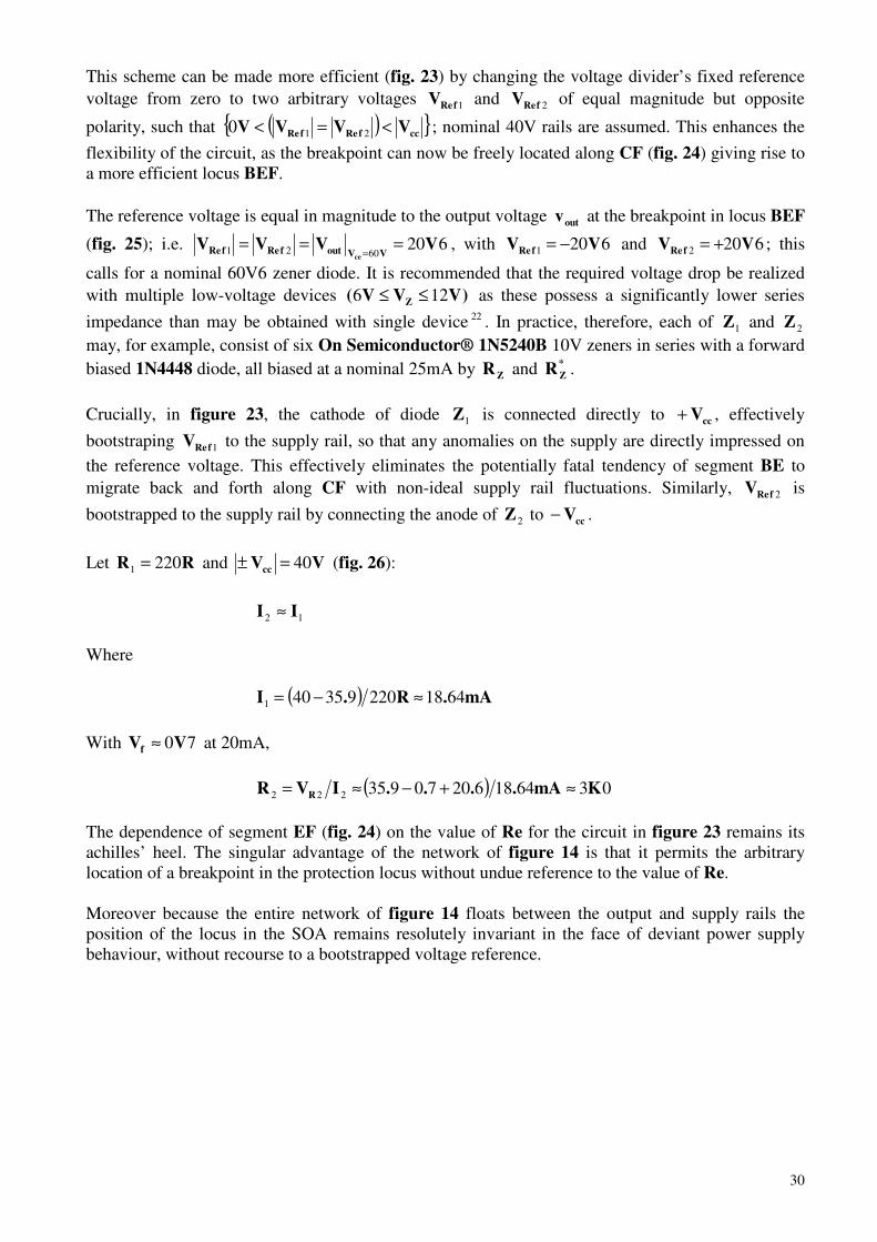
This scheme can be made more efficient (fig. 23) by changing the voltage divider’s fixed reference
voltage from zero to two arbitrary voltages 1fReV and 2fReV of equal magnitude but opposite
polarity, such that ( ) ccfRefRe VVVV <=< 210 ; nominal 40V rails are assumed. This enhances the
flexibility of the circuit, as the breakpoint can now be freely located along CF (fig. 24) giving rise to
a more efficient locus BEF.
The reference voltage is equal in magnitude to the output voltage outv at the breakpoint in locus BEF
(fig. 25); i.e. 6206021 VVVV
VVoutfRefRece
====
, with 6201 VV fRe −= and 6202 VV fRe += ; this
calls for a nominal 60V6 zener diode. It is recommended that the required voltage drop be realized
with multiple low-voltage devices )VVV( Z 126 ≤≤ as these possess a significantly lower series
impedance than may be obtained with single device 22 . In practice, therefore, each of 1Z and 2Z
may, for example, consist of six On Semiconductor® 1N5240B 10V zeners in series with a forward
biased 1N4448 diode, all biased at a nominal 25mA by ZR and *
ZR .
Crucially, in figure 23, the cathode of diode 1Z is connected directly to ccV+ , effectively
bootstraping 1fReV to the supply rail, so that any anomalies on the supply are directly impressed on
the reference voltage. This effectively eliminates the potentially fatal tendency of segment BE to
migrate back and forth along CF with non-ideal supply rail fluctuations. Similarly, 2fReV is
bootstrapped to the supply rail by connecting the anode of 2Z to ccV− .
Let RR 2201 = and VVcc 40=± (fig. 26):
12 II ≈
Where
( ) mA.R.I 6418220935401 ≈−=
With 70VVf ≈ at 20mA,
( ) 03641862070935222 KmA....IVR R ≈+−≈=
The dependence of segment EF (fig. 24) on the value of Re for the circuit in figure 23 remains its
achilles’ heel. The singular advantage of the network of figure 14 is that it permits the arbitrary
location of a breakpoint in the protection locus without undue reference to the value of Re.
Moreover because the entire network of figure 14 floats between the output and supply rails the
position of the locus in the SOA remains resolutely invariant in the face of deviant power supply
behaviour, without recourse to a bootstrapped voltage reference.

31
Fig. 23. The use of arbitrary voltage references of equal magnitude makes for a worthwhile improvement in
efficiency compared to the arrangement of figure 19.

32
Fig. 24. Improved single slope single breakpoint locus BEF realised by using an arbitrary voltage reference.

33
Fig. 25. The reference voltage is made equal in magnitude to the output voltage at the breakpoint (i.e. when
Vce=60V); the diode is then at the threshold of conduction.

34
Fig. 26. Output conditions at point B on the protection locus in figure 24.

35
Dual slope single breakpoint non-linear foldback limiting
Introducing a resistor dR in series with diode 1D (fig. 28) causes the voltage drop across the series
combination to increase linearly above the diode’s conduction threshold. This effectively induces a
net linear increase in potential across resistors 1B
R and 2
R for Ci and cev combinations in the
36ce
v V≥≥≥≥ region of the SOA (fig. 27). The gradient of segment BD in the protection locus can now
be varied linearly 11 with dR about point B which gives vastly greater flexibility with regard to
optimal placement of the breakpoint.
Fig.27. Dual slope single breakpoint non-linear foldback protection locus.
As is the case with single slope linear foldback SOA limiting, segment BD must intersect the SOA’s
Vce axis at a value greater than the sum of the moduli of the supply rails if spurious limiter
activation is to be prevented. Available current per output pair at Vce ≈ 4V is further increased to
12A8 compared to 7A1 for the locus of figure 13.
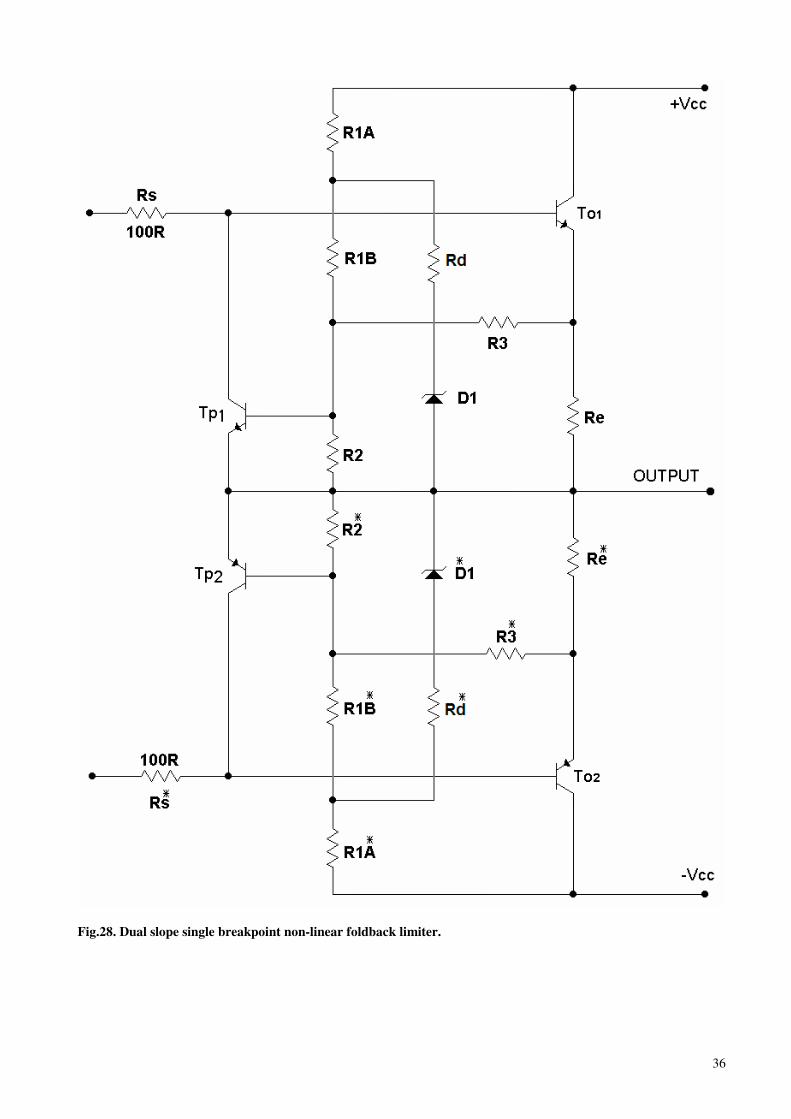
36
Fig.28. Dual slope single breakpoint non-linear foldback limiter.
37
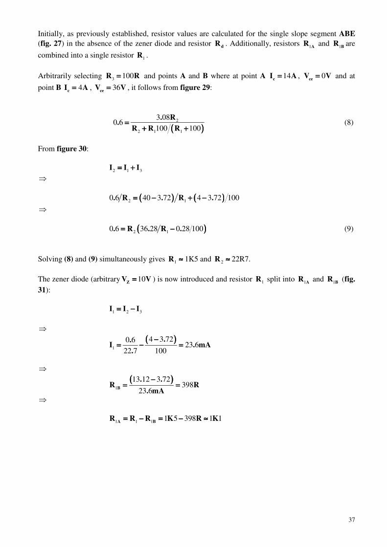
Initially, as previously established, resistor values are calculated for the single slope segment ABE
(fig. 27) in the absence of the zener diode and resistor dR . Additionally, resistors 1A
R and 1B
R are
combined into a single resistor 1
R .
Arbitrarily selecting 3
100R R==== and points A and B where at point A 14c
I A==== , 0ce
V V==== and at
point B 4c
I A==== , 36ce
V V==== , it follows from figure 29:
(((( ))))
2
2 1 1
3 080 6
100 100
. R.
R R R====
+ ++ ++ ++ + (8)
From figure 30:
2 1 3
I I I= += += += +
⇒
(((( )))) (((( ))))2 10 6 40 3 72 4 3 72 100. R . R .= − + −= − + −= − + −= − + −
⇒
(((( ))))2 10 6 36 28 0 28 100. R . R .= −= −= −= − (9)
Solving (8) and (9) simultaneously gives 1R ≈≈≈≈ 1K5 and 2R ≈≈≈≈ 22R7.
The zener diode (arbitrary 10Z
V V==== ) is now introduced and resistor 1R split into 1A
R and 1B
R (fig.
31):
1 2 3
I I I= −= −= −= −
⇒
(((( ))))
1
4 3 720 623 6
22 7 100
..I . mA
.
−−−−= − == − == − == − =
⇒
(((( ))))
1
13 12 3 72398
23 6B
. .R R
. mA
−−−−= == == == =
⇒
1 1 1
1 5 398 1 1A B
R R R K R K= − = − ≈= − = − ≈= − = − ≈= − = − ≈

38
Resistor Rd is now introduced and its value established by consideration of the circuit conditions at
point D ( 0 5c
I . A==== , 79 89ce
V . V==== ) on the locus of figure 27.
Thus from figure 32:
1 2 3B
I I I= += += += +
⇒
(((( ))))
1
39 4 39 890 631 3
22 7 100B
. ..I . mA
.
− +− +− +− += + == + == + == + =
⇒
1 1
39 4 26 9x B B
V . I R . V= − + ≈ −= − + ≈ −= − + ≈ −= − + ≈ −
⇒
(((( ))))
1 1
40 26 931 3 27 5
1 1d A B
.I I I . mA . mA
K
++++= − = − ≈= − = − ≈= − = − ≈= − = − ≈
⇒
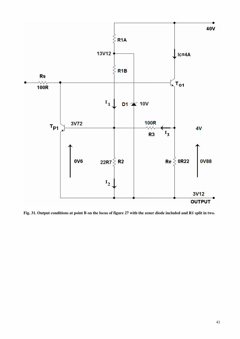
(((( ))))30
111 5x
d
d
VR R
I
++++= ≈= ≈= ≈= ≈

39
Fig. 29. Output conditions at point A on the protection locus of figure 27 in the absence of the zener diode and
resistor Rd.

40
Fig. 30. Output conditions at point B on the locus of figure 27 in the absence of the zener diode and resistor Rd.
41
Fig. 31. Output conditions at point B on the locus of figure 27 with the zener diode included and R1 split in two.

42
Fig. 32. Output conditions at point D on the locus of figure 27 with the resistor Rd introduced.

43
The dual slope single breakpoint scheme of figure 33, sometimes erroneously10 described as “treble
slope” [sic], is an amalgam of the circuits of figures 5 and 19. As in figure 19, the breakpoint occurs
at Vvout 0≈ (i.e. ccce Vv ≈ ) giving locus ADEF (fig. 34). However, segment DEF, being part of
CDEF, is established by 1R and 3R , and its efficacy is therefore as dependent on the value of Re as
the network of figure 5.
Resistor 2R merely pulls the base of the protection transistor low as required for VvV ce 400 <≤ ;
this gives segment AD whose position in the SOA is ill-defined for non-ideal supply rails due to the
use of an invariant voltage reference. Since the breakpoint for this arrangement is fixed at ccce Vv ≈ ,
only points A and F on locus ADEF are required to obtain a solution.
With reference to figure 35, let RR 2203 = and VVcc 40=± :
31 II ≈
Where
mA.R)..(I 73122078394393 ≈+−=
⇒
KmA.).(R 46731439401 ≈+=
With reference to figure 36:
mA.R.)R//R().(I 3311219482523740 312 ≈=−≈
With 70VVf ≈ at 11mA:
333311705237222 KmA.)..(IVR R ≈−==
Clearly, this scheme’s indecent dependence on the value of Re makes it inferior to the standard
linear foldback arrangement of figure 1. Consequently, given Re=0R22, the protection locus of
figure 34 permits the delivery of only 1A5 at Vce ≈ 45V97, requiring a minimum of six output pairs
for unimpeded drive into a )604( 0±∠Ω load from ±40V supply rails.

44
Fig. 33. This dual slope single breakpoint scheme is a logical development of the circuits of figures 5 and 19.

45
Fig. 34. Dual slope single breakpoint loci described by the circuits of figure 33 and 37.

46
Fig. 35. Output conditions at point F on locus ADEF of figure 34.

47
Fig. 36. Output conditions at point A on locus ADEF of figure 34.

48
As with figure 23, the network of figure 33 may be usefully improved (fig. 37) by changing the
diode’s reference from zero to an arbitrary voltage 1fReV such that )VVV( ccfRe << 10 . This
enhances the flexibility of the circuit as the breakpoint can now be moved freely along segment CF,
giving rise to a more efficient locus BEF whose position in the SOA is unaffected by non-ideal
fluctuation of the supply rails (fig. 34).
The reference voltage is established by determining the output conditions at the breakpoint (fig. 38).
Therefore, for locus BEF in figure 34, 33161 VV fRe −= and 33162 VV fRe += , which calls for a
nominal 56V33 zener diode.
With reference to figure 39:
31 II ≈
Where
mA.R)..(I 73122078394393 ≈+−=
⇒
KmA.).(R 46731439401 ≈+=
With reference to figure 40:
mA.R.)R//R().(I 3702196143840 312 ≈=−=
With 650VVf ≈ at 7mA,
47373316650438222 KmA.)...(IVR R ≈+−==
Note that there is no change in the value of 1R and 3R in the circuits of figures 5, 33 and 37, with
different values of 2R required to merely pull the base of the protection transistor low as required
when the diode is forward biased.
Although the efficacy of the protection locus is in part ameliorated by the means described above,
the gradient of segment EF, being part of CDEF, is determined by resistors 1R , 3R and limited by
practical values of Re-an affliction absent from the circuit of figure 28.
49
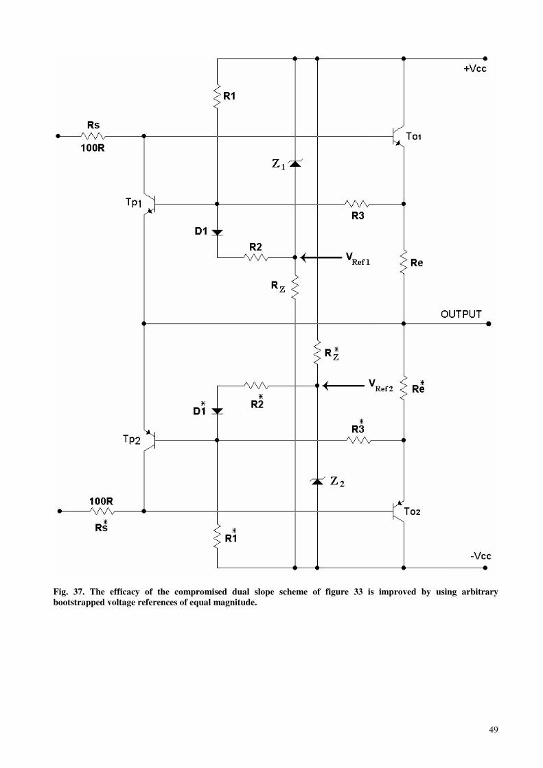
Fig. 37. The efficacy of the compromised dual slope scheme of figure 33 is improved by using arbitrary
bootstrapped voltage references of equal magnitude.

50
Fig. 38. The reference voltage is made equal in magnitude to the output voltage at the breakpoint (i.e. when
Vce=56V); the diode is then at the threshold of conduction.

51
Fig. 39. Output conditions at point F on the protection locus of figure 34.

52
Fig. 40. Output conditions at point B on the protection locus of figure 34.

53
Complete independence from Re of both segments of the dual slope protection locus described by
the circuit of figure 37, may be realised by introducing base-emitter resistors, 2R and ∗2R ,
respectively for each protection transistor, 1PT and 2PT (fig. 41). The result is, in fact, merely a
combination of the linear single slope scheme of figure 1 and the non-linear single slope circuit of
figure 23.
The linear single slope locus of figure 2 is reproduced in figure 42 as segment BCD for which
equations (1) and (3) are valid. Therefore, since, as previously resolved (equations 1 and 3)
RR 2203 = , then 4121 KR = and RR 1432 = (fig. 41). Resistor 4R pulls the base of the protection
transistor low as required for VvV ce 420 ≤≤ giving segment AC.
The reference voltage is equal to the output voltage when Vvce 42= , so that
7722205342401 V)RA(VVV fRe −=∗+−= and 7722 VV fRe += .
With reference to figure 43:
)II()II( 3142 +≈+
⇒
)III(I 2314 −+≈
⇒
R.R).(K).(I 143602209637404129637404 −−+−=
⇒
mA.I 2454 ≈
With 60VVf ≈
mA.)...(IVR R 245772609637444 +−==
⇒
774 KR ≈
The flexibility of the scheme of figure 41 is significantly improved compared to that of figure 37.
However, the network of figure 28 achieves the same versatility with a significantly reduced
component count.

54
Fig. 41. Introducing resistor 2R into the circuit of figure 37 facilitates placement of an arbitrary locus in the
SOA without undue dependence on the value of eR .

55
Fig. 42. Dual slope single breakpoint protection locus described by the circuit of figure 41. Resistor 4R modifies
the linear single slope segment BCD of figure 2 by effecting a vertical translation of segment BC about point C.

56
Fig. 43. Output conditions at point A on protection locus ACD of figure 42.

57
Triple slope dual breakpoint non-linear foldback limiting
With modern power transistors and practical loudspeaker systems, an optimally located dual slope
protection locus realised by the limiter of figure 28 can hardly be improved upon with respect to
efficiency in the critical cccecc VvV 2<≤ region. However, with nominally resistive laboratory
loads, with which a power amplifier’s published specifications are obtained, the ccce VvV ≤≤0
region of the SOA is of primary interest (fig. 10).
Thus, in a competitive market place, even when the truth of the matter is known, an amplifier
designed to maintain its rated voltage swing across resistive loads of decreasing magnitude (typically
to a minimum of 1 ohm) without limiter intrusion may be commercially rewarding. A suitably robust
power supply and conservative thermal management are assumed.
To this end, the triple slope design of figure 44 is presented. This circuit is a straightforward
amalgam of the dual slope scheme of figure 28 and the single slope single breakpoint network of
figure 23. Thus, the circuit of figure 28 is required to produce the dual slope characteristic BDF (fig.
45), while resistor 4R pulls the base of protection transistor 1PT low as appropriate for
VvV ce 420 ≤≤ , giving segment AC.
Fifty-volt supply rails are assumed; a triple slope locus with V40± rails is vastly unnecessary. A
)604( 0±∠Ω load driven to V50± rails requires ≈ci 9A5 when ≈cev 59V, giving peak transistor
dissipation Wp (max)d 561≈ . The triple slope protection locus of figure 45 allows 2A at ≈cev 59V for
a single complementary transistor pair. Therefore, at least five complementary pairs are required to
drive a notional (4Ω ∠ ± 60 0 ) loudspeaker system from V50± supply rails without intrusive limiter
activation. The algebra for this arrangement is straightforward if a little tedious and is left to
interested readers.

58
Fig. 44. Triple slope dual breakpoint non-linear foldback limiter.

59
Fig. 45. Triple slope dual breakpoint protection locus described by the circuit of figure 44; resistor 4R modifies
the dual slope characteristic BDF by effecting a vertical translation of segment BC about point C.

60
Protecting paralleled complementary output transistors
Emitter resistor Re performes current-voltage conversion for the SOA limiter, and promotes thermal
stability by maintaining equable current distribution in an output stage consisting of multiple
paralleled pairs of complementary transistors. For this reason, some designers suggest it is only
neccesary to monitor the current of a single complementary pair in such an output stage .257.pg,1 .
Alternatively, the calculated value of the current sensing resistor 3R for a single complementary
transistor pair is multiplied by the number N of paralleled output pairs with each resistor of value
3RN ∗ used to monitor the current in each transistor as shown in figure 46.
An obvious disadvantage inherent in both schemes is that the open-circuit failure of a rogue
transistor in one half of the output stage could result in the disastrous alteration of the protectection
locus for the remaining devices in that section. However, with modern power transistors, this
condition is unlikely to materialise; the use of an independent SOA limiter for each complementary
pair would eliminate this potential flaw, but is financially indefensible in most commercial designs.

61
Fig. 46. In this single-slope linear foldback scheme, voltage signals from multiple current sensing resistors are
summed algebraically at the base of the protection transistor.

62
Simulating SOA Protection
SPICE allows the designer to check the results of calculation, to establish whether the deviation from
the desired protection locus obtained by using prefered values is significant and to determine the
effect of changes in ambient temperature on the position of the protection locus.
The arrangement of figure 47 is a slightly modified version of the simulation circuit used by Douglas
Self 11 . Voltage source V1 models the output transistors collector-emitter voltage Vce, while the
unity gain voltage controlled current source G1 generates the current in the notional output
transistor’s emitter resistor R6. The current produced by G1 is the quantity that is plotted as V1 is
DC swept. This current is a function of the voltage at the collector of the constant current source
loaded protection transistor Q1.
Unfortunately, results obtained from this circuit can be grossly misleading unless it is correctly
calibrated. This is because an increase in the value of the protection transistor’s constant current
source I1 causes the the plotted locus to move upwards, while an increase in Q1’s current gain
causes the locus to move downwards.
To calibrate the circuit, the single slope linear foldback circuit of figure 1 is used because it gives
inherently more accurate results than the non-linear foldback arrangements whose accuracy is
compromised by zener diodes with tolerances no better than 5%. Thus, having obtained the
calculated values for a given single slope locus, I1 must be adjusted (for a given transistor model for
Q1) until the plotted locus conforms to that predicted by the calculated component values.
Figure 48 shows the effect on the protection locus of increasing the simulation temperature from
27oC to 45oC . This magnitude increase in temperature may occur in the vicinity of the SOA
protection circuitry in, for example, a powerful class-A amplifier.
The drop in threshold voltage (approximately 2 omV / C ) of the protection transistor combined with
the increase (approximately 6 omV / C for a 10V zener diode) in the zener diode’s breakdown
voltage with increasing temperature cause that part of the locus controlled by the zener diode to
move downwards by a significant amount. The 45oC locus can no longer accommodate 40V±±±±
supply rails without protection being invoked, even with an open circuit load, when the output
swings more than about 35V±±±± .
Clearly this effect may be lessened by using a temperature compensated zener diode. Alternatively a
zener diode with negative temperature coefficient may be used to eliminate the downward movement
of the locus which would otherwise be occasioned by the use of a positive temperature coefficient
zener diode and to compensate for the downward movement of the locus due to the protection
transistor’s negative temperature coefficient. This calls for a zener diode with Vz<5V which
typically have a negative temperature coefficient in the range 0 4 omV mV / C−−−− . The potential for
overcompensation is insignificant, but may be accommodated by the judicious placement of that part
of the locus controlled by the zener diode so that any upward movement of the locus with increasing
temperature does not result in the violation of SOA bounds.
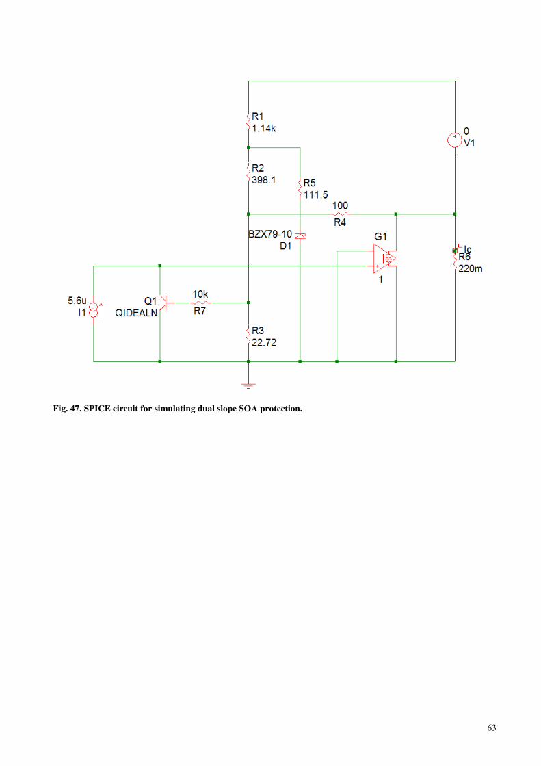
63
Fig. 47. SPICE circuit for simulating dual slope SOA protection.

64
Fig. 48. Simulated loci for the circuit of figure 47 at 27 and 45 degrees Celsius.

65
Conclusion
On grounds of safety and reliability, it is firmly recommended that all nominally linear
complementary semiconductor audio frequency power amplifiers incorporate suitable SOA
protection. The aversion cultivated by some designers to such is here shown to be wholly illusory. A
competently designed SOA limiter should remain demonstrably inert and therefore completely
unobtrusive with virtually all commercial loudspeaker systems provided the output stage consists of
sufficient complementary transistors to safely drive a ( )0604 ±∠Ω load to the supply rails.
The dual slope circuit of figure 28 represents a significant improvement in efficient SOA utilisation
compared to the single slope topology of figure 1, with no significant penalty with regard to
algebraic or physical complexity. Its characteristic locus (fig. 27) may be readily optimised to
accommodate nominal V50± supply rails with MJL3281A/MJL1302A transistors; however,
higher supply rails are not recommended for worst-case reactive loads, as available collector current
for these devices rapidly falls below 0A5 for VVCE 100> .
Although e-MOSFETs are at least an order of magnitude less linear than bipolar transistors .., 27311 pg ,
they provide significantly greater scope for reliable design at high device voltages ( )VVSupply 50>> ,
with the promise of even greater efficiency in SOA utilisation due to the absence of secondary
breakdown. Nevertheless there is no need to endure the indignity of e-MOSFET non-linearity and
on-resistance voltage inefficiency in sub-200W into Ω8 designs.
More elaborate protection schemes are possible, with the use of as many diodes as the number of
required breakpoints. However, the increase in available current in the high voltage
region cccecc VvV 2<≤ , where it counts with respect to reactive load drive, is negligible relative to
the circuit complexity thus engendered.

66
References
1. Slone, R. S., ‘High power audio amplifier construction manual’, McGraw-Hill, ISBN 0-07-
134119-6, pg. 244, and 260.
2. Pass, N. ‘The Pass/A40 power amplifier’. www.passlabs.com
3. Elliot, R., ‘Editorial comment’ on ‘VI limiter’s in amplifiers’, by Allison P. www.sound.au.com
4. Borbely, E., ‘High power, high quality amplifier using MOSFETs.’ Wireless world, March 1983,
pg. 69.
5. Leach, W.M. Jr., ‘Introduction to electroacoustics and audio amplifier design’, 2nd
edition,
Kendal/hunt publishing company, ISBN 0-7872-6093-2, pg. 296.
6. Locher, R., ‘Introduction to power MOSFETs and their applications’. National semiconductor
application note, AN-558, pg. 12. www.national.com
7. Gauen, K., ‘Insuring reliable performance from power MOSFETs’. Motorola application note,
AN929.www.onsemi.com
8. Bailey, A. R., ‘Output transistor protection in audio frequency amplifiers’, Wireless world, June
1968, pg. 155.
9. Stanley, G., Senior Vice-president: Research & Development, Crown Audio. Personal
Communication.
10. Duncan, B., ‘High performance audio power amplifiers’. Newnes, ISBN 0-7506-2629-1, pg. 202,
and pg. 204, fig. 5.23, respectively.
11. Self, D., ‘Audio power amplifier design handbook’, 2nd
edition, Newnes, ISBN 0-7506-4527-X,
pg. 335.
12. Linsley-Hood, J., ‘Valve and transistor audio amplifiers’, Newnes, ISBN 0-7506-3356-5, pg.
165.
13. Self, D., ‘Load-invariant audio power’. Electronics world & wireless world, January 1997, pg.
16.
14. Piper, J.R.I., ‘Output transistor protection in class B amplifiers’, Wireless world, February 1972.
15. www.electronicsworkbench.com
16. Benjamin, E., ‘Audio power amplifiers for loudspeaker loads’. Journal of the audio engineering
society, Vol. 42, #9, September 1994, pg. 670.
17. Sekiya, M., and Otala, M., ‘Load Handling Capability of Commercial Power Amplifiers.’ AES
Preprint #2237, 78th Convention 1985 May 3-6 Anaheim.
18. Cherry, E. M., ‘Ironing out distortion’. Electronics & wireless world, January 1995, pg. 14, &
July 1997, pg. 577.
19. Becker, R. B. H., ‘High-power audio amplifier design’. Wireless world, February 1972, pg. 81.
20. Ruehs, R.G., ‘High power audio amplifiers with short circuit protection’. Motorola application
note, AN485. www.onsemi.com
21. Riedl, A., ‘PA300 power amplifier’, Elektor electronics, November 1995, pg. 60.
22. Motorola TVS/Zener device databook, DL150/D, REV1, Section 11. www.onsemi.com
23. Burwen, R.S., ‘Transistor complementary pair power amplifier with active current limiting
means’. United States patent #3,500,218. 10th
March 1970.
24. Crecraft, D.I., et al, ‘Electronics’, Chapman & Hall, ISBN 0-412-41320-5, pg. 566.
Further Reading
1. Campbell, D.L., ‘Protective circuitry for high fidelity amplifier’. United States patent
#3,526,846. 1st September 1970.
2. Sondermeyer, J.C., ‘Amplifier protection circuit’. United States patent #3,536,959. 27th
October
1970.
3. Fairwood, R.C. and Reed, M.J., ‘Digital measurement and comparison of current-voltage output
capability of amplifiers and demands of loudspeakers’. Journal of the audio engineering society,
Vol. 39. May 1991, Pg.344.