Embed Size (px)
Citation preview
THE RING AMPLIFIER: SCALABLEAMPLIFICATION WITH RING OSCILLATORS
Benjamin Hershberg1 and Un-Ku Moon2
1Imec, Leuven, Belgium2Oregon State University, Corvallis, USA
Abstract
Ring amplification is a technique for performing efficient amplifi-cation in nanoscale CMOS technologies. By using a cascade of dynam-ically stabilized inverter stages to perform accurate amplification, ringamplifiers are able to leverage the key benefits of technology scaling,resulting in excellent efficiency and performance. A generalized viewof basic small-signal theory is first presented, followed by a deeper dis-cussion of the time-domain operation of a ringamp in the context ofa specific ringamp structure. We conclude with a survey of existingringamp implementations and techniques reported in literature.
1. Introduction
In ecology, bio-diversity is often a key indicator of the fitness and resilience ofan ecosystem. In a similar way, the diversity of viable solutions and approachesavailable in the world of analog circuits is an indicator of the health of the analogdesign ecosystem. The range of technical requirements for analog signal process-ing blocks in practical design applications is as broad and vast as the ways inwhich their commercial implementations are used to enhance the many facets ofsociety, work, and leisure. There is no one-size-fits-all solution here. Rather, avariety of solutions allow us to select the best tool for the job and leverage tech-nology scaling to the fullest.
For design in nanoscale CMOS, amplifiers are one area where diversity has ar-guably been lost. Only a small sub-set of the viable amplifier topologies that onceruled in micron and submicron CMOS design remain competitive in nanoscaleCMOS. The impact of this is readily observed in the study of ADCs, whereamplifier-less SAR ADC topologies have been able to leverage technology scal-ing to consistently achieve conversion efficiencies far surpassing ADC topologiesthat rely heavily on amplification [1, 2].
A common misconception is that this poor scaling performance is a fundamentalflaw of amplification itself. In actuality, it is mainly due to an adherence to theold paradigms of how amplifiers should be built. Conventional opamp topologieswere conceived of at a time when 2.5V supplies were considered low-voltage,and the intrinsic properties of transistors were quite different from that of a 14nmFinFET [3]. Transistors were physically much larger with larger internal parasiticcapacitances often approaching even that of the load capacitance being charged.Supply voltages provided much more headroom for stacking devices, and intrinsicdevice gains were higher. All these factors created a design world where cascod-ing was preferable to cascading, current biasing was necessary, and small-signalanalysis was the prevailing and sufficient design paradigm.
Since those times, a lot has changed. Semiconductor technology has continued toevolve in a direction aimed at improving density, efficiency, and speed for digi-tal logic gates. The ability of a conventional opamp topology to flourish in thisnew environment is fundamentally limited due to inherent incompatibilities in theunderlying approach. Applying additional techniques such as calibration, gain-enhancement, and output-swing enhancement may enable an opamp to functionin nanoscale environments, but it won’t grant it the ability to scale at the samepace as digital performance improvements. A truly scalable amplifier must oper-ate natively in its environment, in a way that implicitly uses the characteristics ofscaled CMOS to its advantage, transforming potential weaknesses into inherentstrengths. Since technology scaling is deliberately designed to favor the time-domain world of high-speed digital, viable nanoscale analog techniques are likelyto be found in the time-domain realm as well. In order to fully exploit the abil-ities of a transistor, the biasing and small-signal properties of the device mustbe viewed as highly coupled, time-dependent variables which can be applied asfeedback to each other with respect to time.
Here we explore one such technique: ring amplification. A ring amplifier (ringamp,RAMP) is a small modular amplifier derived from a ring oscillator which naturallyembodies all the essential elements of scalability. It can amplify with rail-to-railoutput swing, efficiently charge large capacitive loads using slew-based charging,scale well in performance according to process trends, and is simple enough to bequickly constructed from only a handful of inverters, capacitors, and switches.
2. A small-signal, steady-state perspective
The transient, large-signal, and small-signal operation domains are often muchmore interdependent in ring amplifier toplogies than classical amplifier topolo-
VIN -VDZ
+
VOUT
RST RST
RST
C1
C3
C2
MCP
MCN
VOUTVIN
VOUTVIN
CLp1 p2 p3
HSTAB(V,t) HSTAB(V,t) HSTAB(V,t) HSTAB(V,t)
(a)
p1 p2 p3
VOUT
CL
VIN
(b)
100
102
104
106
108
1010
1012
1014
−300
−200
−100
0
100
UGBW: 3.98 GHz
PM: 45.06
p1: 8 GHz p2: 12 GHz
p3: 2.35 MHz
f1:f3 ratio: 3396
frequency (Hz)
Mag
nitu
de (
dB/d
eg)
(c)
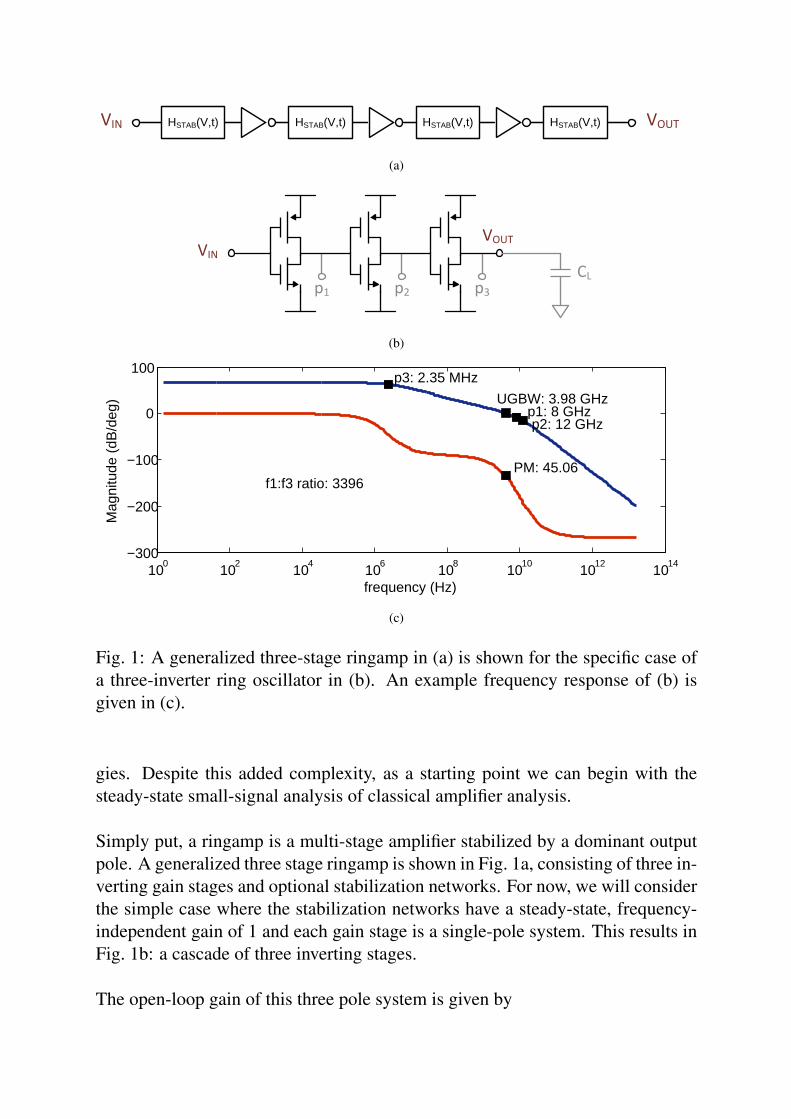
Fig. 1: A generalized three-stage ringamp in (a) is shown for the specific case ofa three-inverter ring oscillator in (b). An example frequency response of (b) isgiven in (c).
gies. Despite this added complexity, as a starting point we can begin with thesteady-state small-signal analysis of classical amplifier analysis.
Simply put, a ringamp is a multi-stage amplifier stabilized by a dominant outputpole. A generalized three stage ringamp is shown in Fig. 1a, consisting of three in-verting gain stages and optional stabilization networks. For now, we will considerthe simple case where the stabilization networks have a steady-state, frequency-independent gain of 1 and each gain stage is a single-pole system. This results inFig. 1b: a cascade of three inverting stages.
The open-loop gain of this three pole system is given by
H(s) =gm1ro1 · gm2ro2 · gm3ro3
(1 + sro1Cp1)(1 + sro2Cp2)(1 + sro3(Cp3 + CL))(1)
where rox is the impedance seen at pole/node X, gmx is the trans-conductance ofinverter stage X, and Cpx is the total capacitance seen at pole/node X.
Recalling basic stabilization theory, in order to transform this structure from anunstable ring oscillator into a stable ring amplifier, we must create a sufficientlylarge ratio between the lowest frequency pole in the system and the higher fre-quency poles. Given that an external load capacitance is required for any prac-tical switched-capacitor design scenario, it is then relatively simple to prove thatthe strategy of stabilizing with a dominant output pole (p3) will always yield themaximum amplifier bandwidth and highest efficiency.
The optimal output pole location can be created by first placing p1 and p2 at thehighest frequencies possible and then adjusting the location of p3 until it is at asufficiently low, stabilizing frequency. Critically, for a three-stage opamp usingconventional techniques and current biasing, this would not yield a very practi-cal solution. The internal poles would still be relatively large, which would limitbandwidth and require an often impractically large explicit load capacitance at theoutput. Miller-compensation can be used to make other poles in the system dom-inant instead, but at high price in terms of bandwidth and efficiency. In the caseof a ringamp with very small transistors used in gain stages 1 and 2 and dynamicbiasing (i.e. just a basic inverter in this case), output pole stabilization becomesa realistic possibility. Poles p1 and p2 can be placed at very high frequencies,which allows us to place p3 at a sufficiently stable location using a much morereasonably sized load capacitance.
This analysis describes the steady-state condition that a ringamp must reach inorder to stabilize, but it does not tell us anything about how it does it. In manyapplication scenarios, Fig. 1b is not the optimal implementation, and may not evenbe capable of meeting the required performance specs. At this point it is worthrevisiting Fig. 1a and re-considering the “how” of ringamp stabilization. In thenext section, we will take a closer look at a particular ringamp structure that usestime-domain feedback to dynamically adjust the output pole location and therebyrelax stability constraints. Afterwards, in Section 4, we will look at other existingsolutions, including techniques to extend ringamp operation into high accuracyapplications.
RS
T
VCMX
RST RST
RST
MCP
MCN
+ VOS -
- VOS +
VCM - VOS
VBP
VBN
VA
VIN VOUT
Ring Amplifier
C2
C1
C3
VCM + VOS
CLOAD
RST
VCMO
VIN
VDAC
RST(Example MDAC Feedback Structure)
A2
A1
A2
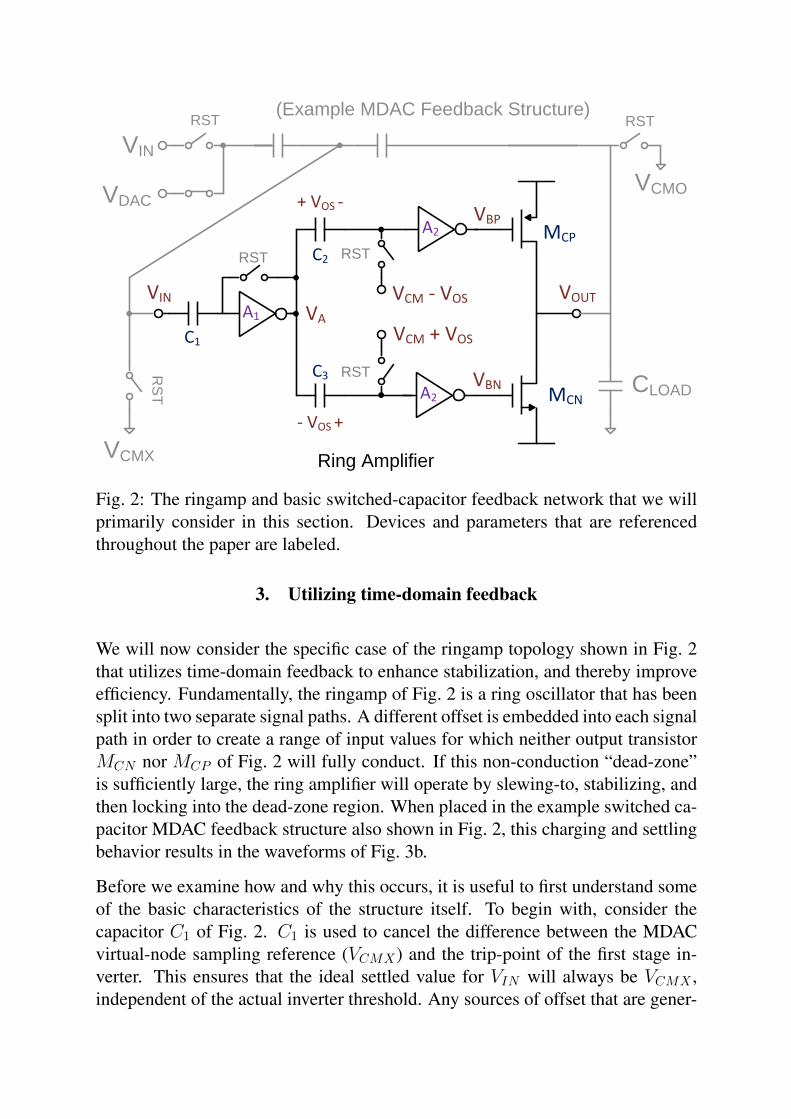
Fig. 2: The ringamp and basic switched-capacitor feedback network that we willprimarily consider in this section. Devices and parameters that are referencedthroughout the paper are labeled.
3. Utilizing time-domain feedback
We will now consider the specific case of the ringamp topology shown in Fig. 2that utilizes time-domain feedback to enhance stabilization, and thereby improveefficiency. Fundamentally, the ringamp of Fig. 2 is a ring oscillator that has beensplit into two separate signal paths. A different offset is embedded into each signalpath in order to create a range of input values for which neither output transistorMCN nor MCP of Fig. 2 will fully conduct. If this non-conduction “dead-zone”is sufficiently large, the ring amplifier will operate by slewing-to, stabilizing, andthen locking into the dead-zone region. When placed in the example switched ca-pacitor MDAC feedback structure also shown in Fig. 2, this charging and settlingbehavior results in the waveforms of Fig. 3b.
Before we examine how and why this occurs, it is useful to first understand someof the basic characteristics of the structure itself. To begin with, consider thecapacitor C1 of Fig. 2. C1 is used to cancel the difference between the MDACvirtual-node sampling reference (VCMX) and the trip-point of the first stage in-verter. This ensures that the ideal settled value for VIN will always be VCMX ,independent of the actual inverter threshold. Any sources of offset that are gener-
0 1 2 3 4 5 60
0.2
0.4
0.6
0.8
1
1.2
time (ns)
Volts
VIN
VOUT
y-axis zoom of VIN
0 2 4 6
0.58
0.6
0.62
Volts
time (ns)
VDZ = 0mV
(a)
0 1 2 3 4 5 60
0.2
0.4
0.6
0.8
1
1.2
time (ns)
Volts
VIN
VOUT
VDZ = 170mV
0 2 4 6
0.58
0.6
0.62
Volts
time (ns)
y-axis zoom of VIN
(b)
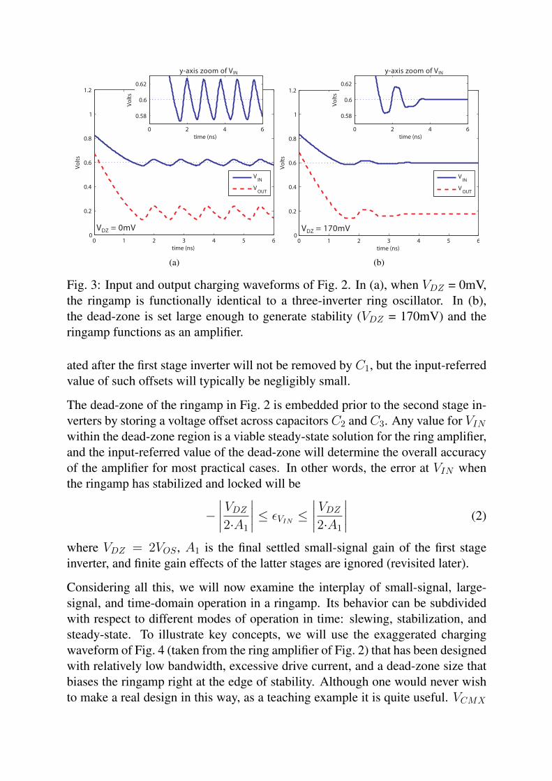
Fig. 3: Input and output charging waveforms of Fig. 2. In (a), when VDZ = 0mV,the ringamp is functionally identical to a three-inverter ring oscillator. In (b),the dead-zone is set large enough to generate stability (VDZ = 170mV) and theringamp functions as an amplifier.
ated after the first stage inverter will not be removed by C1, but the input-referredvalue of such offsets will typically be negligibly small.
The dead-zone of the ringamp in Fig. 2 is embedded prior to the second stage in-verters by storing a voltage offset across capacitors C2 and C3. Any value for VINwithin the dead-zone region is a viable steady-state solution for the ring amplifier,and the input-referred value of the dead-zone will determine the overall accuracyof the amplifier for most practical cases. In other words, the error at VIN whenthe ringamp has stabilized and locked will be
−∣∣∣∣VDZ2·A1
∣∣∣∣ ≤ εVIN ≤∣∣∣∣VDZ2·A1
∣∣∣∣ (2)
where VDZ = 2VOS , A1 is the final settled small-signal gain of the first stageinverter, and finite gain effects of the latter stages are ignored (revisited later).
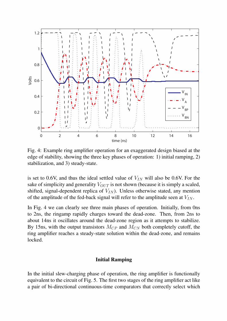
Considering all this, we will now examine the interplay of small-signal, large-signal, and time-domain operation in a ringamp. Its behavior can be subdividedwith respect to different modes of operation in time: slewing, stabilization, andsteady-state. To illustrate key concepts, we will use the exaggerated chargingwaveform of Fig. 4 (taken from the ring amplifier of Fig. 2) that has been designedwith relatively low bandwidth, excessive drive current, and a dead-zone size thatbiases the ringamp right at the edge of stability. Although one would never wishto make a real design in this way, as a teaching example it is quite useful. VCMX
0 2 4 6 8 10 12 14 16
0
0.2
0.4
0.6
0.8
1
1.2Vo
lts
time (ns)
VIN
VA
VBP
VBN
Fig. 4: Example ring amplifier operation for an exaggerated design biased at theedge of stability, showing the three key phases of operation: 1) initial ramping, 2)stabilization, and 3) steady-state.
is set to 0.6V, and thus the ideal settled value of VIN will also be 0.6V. For thesake of simplicity and generality VOUT is not shown (because it is simply a scaled,shifted, signal-dependent replica of VIN ). Unless otherwise stated, any mentionof the amplitude of the fed-back signal will refer to the amplitude seen at VIN .
In Fig. 4 we can clearly see three main phases of operation. Initially, from 0nsto 2ns, the ringamp rapidly charges toward the dead-zone. Then, from 2ns toabout 14ns it oscillates around the dead-zone region as it attempts to stabilize.By 15ns, with the output transistors MCP and MCN both completely cutoff, thering amplifier reaches a steady-state solution within the dead-zone, and remainslocked.
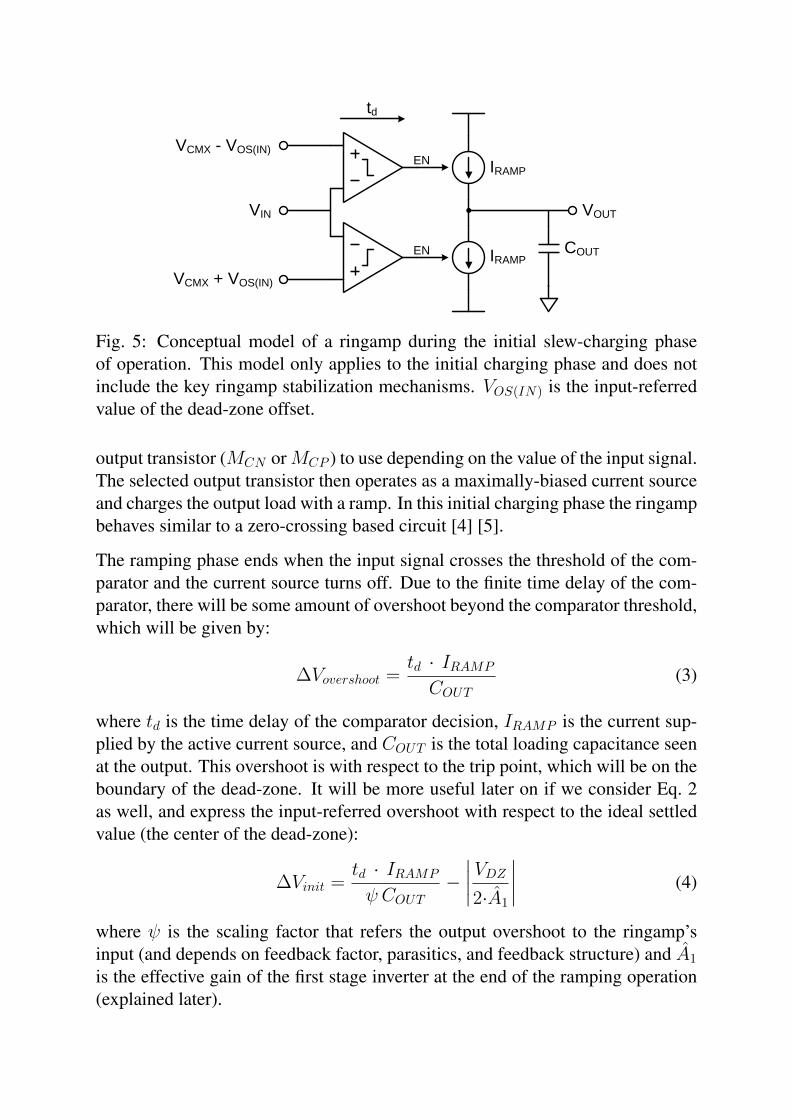
Initial Ramping
In the initial slew-charging phase of operation, the ring amplifier is functionallyequivalent to the circuit of Fig. 5. The first two stages of the ring amplifier act likea pair of bi-directional continuous-time comparators that correctly select which
VIN
VCMX - VOS(IN)
IRAMP
VOUT
EN
EN
VCMX + VOS(IN)
td
COUTIRAMP
Fig. 5: Conceptual model of a ringamp during the initial slew-charging phaseof operation. This model only applies to the initial charging phase and does notinclude the key ringamp stabilization mechanisms. VOS(IN) is the input-referredvalue of the dead-zone offset.
output transistor (MCN orMCP ) to use depending on the value of the input signal.The selected output transistor then operates as a maximally-biased current sourceand charges the output load with a ramp. In this initial charging phase the ringampbehaves similar to a zero-crossing based circuit [4] [5].
The ramping phase ends when the input signal crosses the threshold of the com-parator and the current source turns off. Due to the finite time delay of the com-parator, there will be some amount of overshoot beyond the comparator threshold,which will be given by:
∆Vovershoot =td · IRAMP
COUT(3)
where td is the time delay of the comparator decision, IRAMP is the current sup-plied by the active current source, and COUT is the total loading capacitance seenat the output. This overshoot is with respect to the trip point, which will be on theboundary of the dead-zone. It will be more useful later on if we consider Eq. 2as well, and express the input-referred overshoot with respect to the ideal settledvalue (the center of the dead-zone):
∆Vinit =td · IRAMP
ψ COUT−
∣∣∣∣VDZ2·A1
∣∣∣∣ (4)
where ψ is the scaling factor that refers the output overshoot to the ringamp’sinput (and depends on feedback factor, parasitics, and feedback structure) and A1
is the effective gain of the first stage inverter at the end of the ramping operation(explained later).
Stabilization
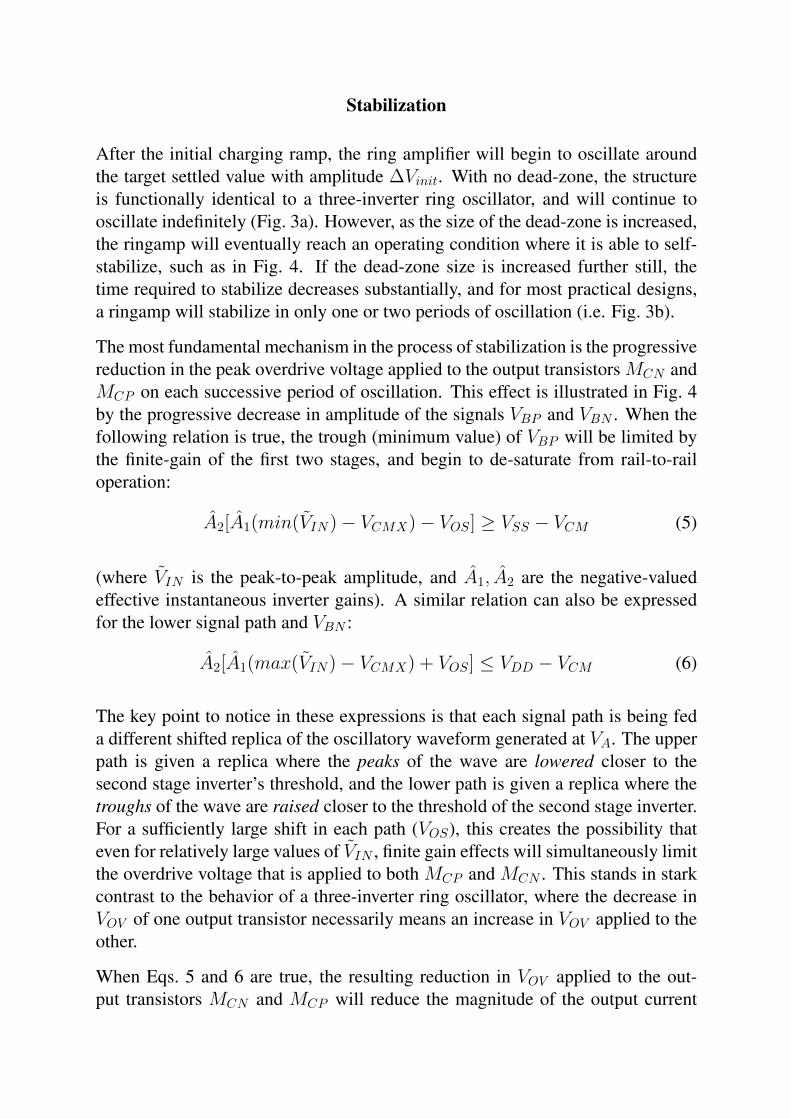
After the initial charging ramp, the ring amplifier will begin to oscillate aroundthe target settled value with amplitude ∆Vinit. With no dead-zone, the structureis functionally identical to a three-inverter ring oscillator, and will continue tooscillate indefinitely (Fig. 3a). However, as the size of the dead-zone is increased,the ringamp will eventually reach an operating condition where it is able to self-stabilize, such as in Fig. 4. If the dead-zone size is increased further still, thetime required to stabilize decreases substantially, and for most practical designs,a ringamp will stabilize in only one or two periods of oscillation (i.e. Fig. 3b).
The most fundamental mechanism in the process of stabilization is the progressivereduction in the peak overdrive voltage applied to the output transistors MCN andMCP on each successive period of oscillation. This effect is illustrated in Fig. 4by the progressive decrease in amplitude of the signals VBP and VBN . When thefollowing relation is true, the trough (minimum value) of VBP will be limited bythe finite-gain of the first two stages, and begin to de-saturate from rail-to-railoperation:
A2[A1(min(VIN)− VCMX)− VOS] ≥ VSS − VCM (5)
(where VIN is the peak-to-peak amplitude, and A1, A2 are the negative-valuedeffective instantaneous inverter gains). A similar relation can also be expressedfor the lower signal path and VBN :
A2[A1(max(VIN)− VCMX) + VOS] ≤ VDD − VCM (6)
The key point to notice in these expressions is that each signal path is being feda different shifted replica of the oscillatory waveform generated at VA. The upperpath is given a replica where the peaks of the wave are lowered closer to thesecond stage inverter’s threshold, and the lower path is given a replica where thetroughs of the wave are raised closer to the threshold of the second stage inverter.For a sufficiently large shift in each path (VOS), this creates the possibility thateven for relatively large values of VIN , finite gain effects will simultaneously limitthe overdrive voltage that is applied to both MCP and MCN . This stands in starkcontrast to the behavior of a three-inverter ring oscillator, where the decrease inVOV of one output transistor necessarily means an increase in VOV applied to theother.
When Eqs. 5 and 6 are true, the resulting reduction in VOV applied to the out-put transistors MCN and MCP will reduce the magnitude of the output current
IRAMP . This decrease in output current will also cause a decrease in the ampli-tude of VIN by a proportional amount, due to Eq. 4. The left sides of Eqs. 5 and 6are therefore reduced further, and the VOV ’s ofMCN andMCP will decrease evenmore for the next oscillation cycle. This effect will continue to feedback until theinput signal amplitude becomes smaller than the input-referred value of the dead-zone, at which point the ring amplifier will stabilize and lock into the dead-zone.
If we combine Eqs. 5 and 6 and rearrange, we see that in order to trigger thisprogressive overdrive reduction effect, the input signal must satisfy the followingrelation:
VIN ≤1
A1
(VDD − VSS
A2
− VDZ). (7)
Furthermore, at the beginning of the stabilization phase:
VIN = 2·∆Vinit (8)
Finally, using Eqs. 3, 4, 7, and 8, we can express the stability criterion in terms ofthe dead-zone (i.e. settled accuracy) and the initial slew rate (i.e. speed):
td · IRAMP
ψ COUT≤ 1
2·A1
(VDD − VSS
A2
− 2·VDZ)
(9)
Recall once again that A1 and A2 are negative valued gains.
From this relation we see that there is a clear design tradeoff between accuracy,speed, and power. Let’s assume for a moment that only td, IRAMP , and VDZcan be adjusted. To increase speed, one can either increase the initial ramp rateor decrease the time required to stabilize. Both options require sacrificing eitheraccuracy (by increasing VDZ) or power (by decreasing td). Likewise, to increaseaccuracy (by decreasing VDZ), one must either decrease IRAMP or decrease tdaccordingly. While these simple tradeoffs serve as a good starting point, as wewill soon discover, every parameter in Eq. 9 is variable to some extent.
The discussion thus far is only a first-order model, and there are additional band-width, slewing, and device biasing dynamics which are not represented. Let’stake a moment to evaluate this model in the form of a practical example. Con-sider a pseudo-differential ringamp where A1 = A2 = −25VV , VDZ = 100mV ,VDD = 1.2V , and VSS = 0V . By Eq. 2, the input-referred size of the dead-zonewill be about 4mV, which for a 2V pk-pk input signal would ideally be accu-rate enough to achieve an input-referred SNDR of 54dB. By Eq. 7, the maximumallowable peak-to-peak amplitude of VIN is approximately 6mV, and by Eq. 4,the maximum allowable input-referred overshoot at the end of the initial rampingphase must be less than 5mV.
This isn’t a very encouraging result, since such a small overshoot will place atight constraint on the parameters in Eq. 3. However, if one were to simulate thissame scenario, it will turn out that the peak-to-peak amplitude of oscillation canbe significantly larger than the predicted 6mV and still achieve stability. A closerlook at Fig. 4 reveals an important contributor to this disparity between theory andpractice. Although the AC small-signal gain of the first stage inverter, A1, may be−25VV , the effective instantaneous value
A1(t) =VA(t)
VIN(t)(10)
in the actual transient waveform will be several times smaller at the beginning ofstabilization. Thus, although the overall accuracy of the ringamp is determinedby the final, settled, small-signal value of A1, the stability criterion is determinedby the initial, transient, large signal effective value of A1. This reduction in A1
occurs because the first stage inverter inherently operates around its trip point,where it will be slew limited. The maximum slewing current that the inverter canprovide will be
Islew = IP − IN (11)
and for a square law MOSFET model, this will become:
Islew = 2k′W
L
(VDD − VSS
2
)VIN (12)
Notice here that the slew current is linearly related (not quadratically) to the inputvoltage. Thus, for the first stage inverter, slew rate limiting (and finite bandwidth)has an important impact on determining the effective value of A1 during stabi-lization (and to a lesser extent, the value of A2). This dynamic adjustment ofthe effective inverter gain is a very attractive characteristic, and improves the de-sign tradeoff between speed, accuracy, and power by a significant factor. Similareffects also influence the operation of the second stage inverters in an additionalway: although Eqs. 5 and 6 assume rail-to-rail swing for the second stage inverterswhen VIN is large, in reality the output swing of the second stage inverters maynever completely reach rail-to-rail, regardless of the value of VIN due to slew ratelimiting, finite bandwidth, and triode device operation.
Relating the discussion of progressive overdrive reduction in this section back tothe steady-state stability discussion of Section 2, this behavior can be conceptual-ized as a dynamic adjustment of the ringamp’s output pole corner frequency. Thedecrease in output current due to VOV reduction increases the output impedance(Ro) of the ringamp, and pushes the output pole (formed by Ro and CLOAD) tolower frequency. As the VOV reduction effect gains momentum on each succes-sive oscillation half-period, the output pole progressively pushes to lower and
-10 -5 0 5 10
-0.2
-0.1
0
0.1
0.2
Vin
(mV)
I out (m
A)
lower stabilitythreshold
upper stabilitythreshold
weak-zone
dead-zone
stability region
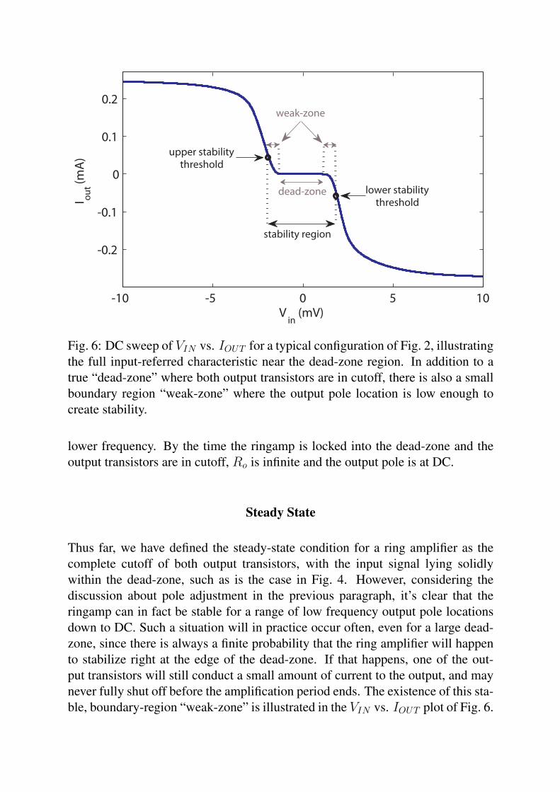
Fig. 6: DC sweep of VIN vs. IOUT for a typical configuration of Fig. 2, illustratingthe full input-referred characteristic near the dead-zone region. In addition to atrue “dead-zone” where both output transistors are in cutoff, there is also a smallboundary region “weak-zone” where the output pole location is low enough tocreate stability.
lower frequency. By the time the ringamp is locked into the dead-zone and theoutput transistors are in cutoff, Ro is infinite and the output pole is at DC.
Steady State
Thus far, we have defined the steady-state condition for a ring amplifier as thecomplete cutoff of both output transistors, with the input signal lying solidlywithin the dead-zone, such as is the case in Fig. 4. However, considering thediscussion about pole adjustment in the previous paragraph, it’s clear that theringamp can in fact be stable for a range of low frequency output pole locationsdown to DC. Such a situation will in practice occur often, even for a large dead-zone, since there is always a finite probability that the ring amplifier will happento stabilize right at the edge of the dead-zone. If that happens, one of the out-put transistors will still conduct a small amount of current to the output, and maynever fully shut off before the amplification period ends. The existence of this sta-ble, boundary-region “weak-zone” is illustrated in the VIN vs. IOUT plot of Fig. 6.
The weak-zone isn’t an inherent problem for ring amplification operation, sinceany low-bandwidth settling will only serve to further improve accuracy. However,there are sometimes higher-level structural considerations that make it advanta-geous to ensure that both output transistors are completely non-conducting oncesettled. We will see some designs where this is the case later on, in Section 4.
3.1. Key Advantages
Ring amplifiers are in many ways both structurally and functionally quite differ-ent from conventional opamps, and it is in these differences that the ringamp findsa unique advantage in the context of modern low-voltage CMOS process tech-nologies. In this section, we will examine several of these important benefits ingreater detail.
Output Compression Immunity
In low-voltage scaled environments, kT/C noise, SNR, and power constraints willtypically be dictated by the usable signal range available [1], and any practicalamplification solution for scaled CMOS must therefore utilize as much of theavailable voltage range as possible. As it turns out, ring amplifiers are almostentirely immune to output compression, and this enables them to amplify withrail-to-rail output swing.
To understand the basis of this output compression immunity, we must considertwo scenarios. First, imagine a ringamp whose dead-zone is large enough thatwhen the ringamp is locked into the center of the dead-zone, both MCN andMCP
will be in cutoff. In other words, when:
VDZ ≥∣∣∣∣VDD − VSS − 2VT
A2
∣∣∣∣ (13)
As a rule of thumb, this relation will usually hold for low and medium accuracyringamps up to about 60dB. Under this scenario, MCN and MCP function as cur-rent sources whose linearity and small-signal gain has no appreciable effect onsettled accuracy. The internal condition of the ringamp depends only on the sig-nal at the input, and it will continue to steer toward the dead-zone until MCN andMCP are completely cut-off, regardless of whether they are in saturation or triode.Final settled accuracy will be governed by Eq. 2, independent of the characteris-tics at the output.
Now let’s consider the condition where Eq. 13 does not hold. This will occurwhen the dead-zone is very small, and accuracies in the 60dB to 90dB range aredesired. Although other practical issues in the ringamp structure of Fig. 2 mayhinder such design targets, we will consider a ringamp structure later in Section 4where it applies. In this scenario, the stability region of Fig. 6 is so small that thetwo weak-zones touch, andMCN andMCP will still conduct a small amount oncesettled. The ringamp’s steady state condition will essentially be that of a threestage opamp, and the open loop gain will be the product of the three stage gains.With no true dead-zone, the distortion term of Eq. 2 becomes zero, and finiteloop gain will become the fundamental limitation on accuracy. At first glance,generating sufficient loop gain appears to be a problem, since the gain of MCN
and MCP will depend on output swing (which must be as large as possible innanoscale CMOS). Consider the case where all three stages have a gain of 25dBwhen operating in saturation. In the best case, the open loop gain will be 75dB,and in the worst case perhaps 50dB. Even in the best case, this seems to suggestthat to build an 80dB accurate ringamp, an additional gain stage is required.
Luckily, there is another effect at play here. In the ideal square-law MOSFETmodel MCN and MCP will be in saturation when VOV < VDS . Furthermore,the small signal output impedance, ro, is inversely proportional to the drain cur-rent, ID. In the context of the progressive overdrive voltage reduction that oc-curs in ringamp stabilization, both VOV and ID will in fact trend towards zero.This implies that during steady-state, MCN and MCP will remain in saturation orweak-inversion even for very small values of VDS , and moreover, that their gainwill be enhanced by a dynamic boost in ro. Thus, even for a nominal open loopgain of 75dB, with a wisely chosen topology it is possible to have an enhancedsteady-state gain of at least 90dB, even when swinging close to the rails.
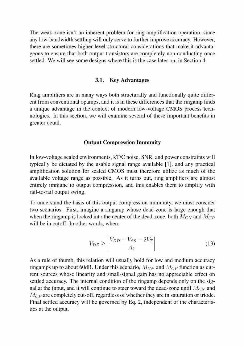
Although output swing has little effect on ringamp accuracy, it will indeed affectspeed, both with respect to slewing and settling. In the initial ramping phase,the selected current source transistor will be biased with the maximum possibleVOV , and this guarantees that for much of the possible output range it will initiallybe operating in triode. As seen in Fig. 7, for settled output values near mid-rail,IRAMP will be the highest and the initial ramping will be faster, but more timewill be required to stabilize for the reasons discussed in Section 3. Likewise, forvalues close to the rails, IRAMP will be smaller, so the initial ramping will beslower but the stabilization time will be shorter. For the most part, this worksout quite nicely, since the total time required to reach steady state in each caseturns out to be approximately the same. However, for extreme cases very closeto the rails, the large RC time constant of the output transistor in triode operationwill require a comparatively long time to reach its target value. Ultimately, it is
0 1 2 3 4 5 6 70.55
0.6
0.65Vo
lts
time (ns)
Small SwingMedium SwingLarge Swing
Fig. 7: Zoomed stabilization waveform of VIN for three output swing cases: small(output near mid-rail), medium, and large (final output near the supply).
this RC settling limitation that will usually dictate the maximum output swingpossible for a given speed of operation.
Slew-Based Charging
Whereas a conventional opamp charges its output load with some form of RC-based settling, the output transistors MCN and MCP in the ring amplifier behavelike digitally switched current sources, and charge the output with slew-basedramping. This is a much more efficient way to charge, since only one of thecurrent sources in Fig. 5 will be active at a time, and the only power dissipatedwill be dynamic. Furthermore, during the initial ramping operation, MCN orMCP (whichever is selected) will be biased with the maximum VOV possible forthe given supply voltage. This is a major benefit, because it means that even forlarge capacitive loads, small transistor sizes can still produce high slew rates, andwith small output transistors, the second stage inverters will be negligibly loadedby MCN /MCP . This effectively decouples the internal power requirements fromthat of the output load size, and for typical load capacitances in the femto andpico-farad range, the internal power requirements are more-or-less independentof output capacitance. This unique property stands in stark contrast to the power-loading relationship for a conventional opamp, where settling speed is typically
proportional to gm/CLOAD. Even for large load capacitances, where the size ofMCN /MCP does have an appreciable effect on the internal power requirements,the ratio of static-to-dynamic power will scale very favorably.
Performance Scaling with Process
In order for a technique to be truly scalable, it must meet two criteria. First, thegiven technique must operate efficiently in a scaled environment. This require-ment has been our primary focus thus far. Second, the technique must inherentlyscale with advancing process technology, improving in performance simply bymigrating into a newer technology. It is this second criteria that we will discussnow.
Intuitively, the ring amplifier seems like a prime candidate to benefit from processscaling, simply due to its structural similarity to a ring oscillator. The stabil-ity criterion of Eq. 9 suggests this to be true. As stated previously, the internalpower consumption of a ringamp is governed much more by inverter power-delayproduct and internal parasitics than the size of the output load (in stark contrast toconventional opamps). Since the power-delay product of an inverter decreases ap-proximately linearly in accordance with decreasing feature size [6], the ringamp’sinverter chain propagation delay, td, can be expected to scale according to digi-tal process performance as well. With the relationships in Eq. 9, this reductionin td can be directly traded for an improvement in any of the three main designspecifications: speed, accuracy, and power.
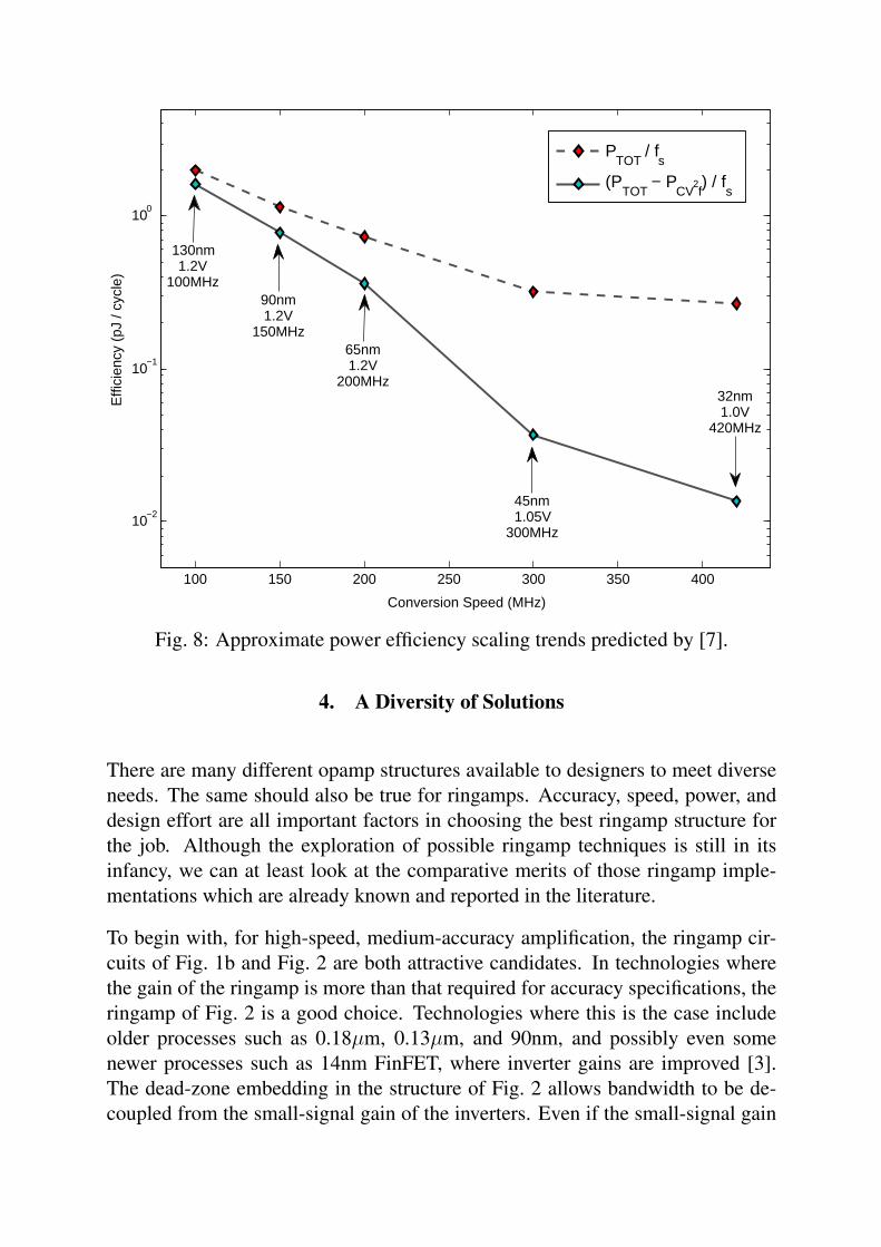
The simple scaling experiment conducted in [7] suggests that this is indeed thecase. The results of the test are shown in Fig. 8. The upper trend line representspredicted power efficiency with the power spent in charging the fixed (not scaled)load capacitance included. The lower trend line shows the power efficiency withthe ideal power required to charge the load capacitance subtracted out. The re-sult is a power efficiency trend that scales very well with advancing technologynode. Although there are not yet enough measured ringamp designs to verify pre-dicted trend, we do see a similar level of speed and efficiency scaling between the0.18µm CMOS design of [8] and the 65nm CMOS design of [9]. Furthermore,recent investigations of ringamp structures in 28nm CMOS have produced resultsthat also support this hypothesis.
100 150 200 250 300 350 400
10−2
10−1
100
Conversion Speed (MHz)
Effi
cien
cy (
pJ /
cycl
e)Ring Amplifier Scalability
PTOT
/ fs
(PTOT
− PCV
2f) / f
s
130nm1.2V
100MHz90nm1.2V
150MHz65nm1.2V
200MHz32nm1.0V
420MHz
45nm1.05V
300MHz
Fig. 8: Approximate power efficiency scaling trends predicted by [7].
4. A Diversity of Solutions
There are many different opamp structures available to designers to meet diverseneeds. The same should also be true for ringamps. Accuracy, speed, power, anddesign effort are all important factors in choosing the best ringamp structure forthe job. Although the exploration of possible ringamp techniques is still in itsinfancy, we can at least look at the comparative merits of those ringamp imple-mentations which are already known and reported in the literature.
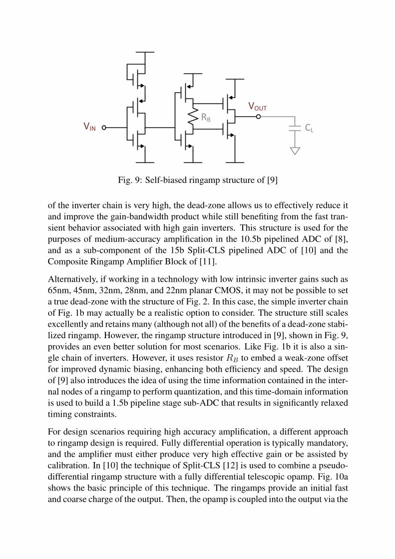
To begin with, for high-speed, medium-accuracy amplification, the ringamp cir-cuits of Fig. 1b and Fig. 2 are both attractive candidates. In technologies wherethe gain of the ringamp is more than that required for accuracy specifications, theringamp of Fig. 2 is a good choice. Technologies where this is the case includeolder processes such as 0.18µm, 0.13µm, and 90nm, and possibly even somenewer processes such as 14nm FinFET, where inverter gains are improved [3].The dead-zone embedding in the structure of Fig. 2 allows bandwidth to be de-coupled from the small-signal gain of the inverters. Even if the small-signal gain
VOUT
CLVIN
RB
Fig. 9: Self-biased ringamp structure of [9]
of the inverter chain is very high, the dead-zone allows us to effectively reduce itand improve the gain-bandwidth product while still benefiting from the fast tran-sient behavior associated with high gain inverters. This structure is used for thepurposes of medium-accuracy amplification in the 10.5b pipelined ADC of [8],and as a sub-component of the 15b Split-CLS pipelined ADC of [10] and theComposite Ringamp Amplifier Block of [11].
Alternatively, if working in a technology with low intrinsic inverter gains such as65nm, 45nm, 32nm, 28nm, and 22nm planar CMOS, it may not be possible to seta true dead-zone with the structure of Fig. 2. In this case, the simple inverter chainof Fig. 1b may actually be a realistic option to consider. The structure still scalesexcellently and retains many (although not all) of the benefits of a dead-zone stabi-lized ringamp. However, the ringamp structure introduced in [9], shown in Fig. 9,provides an even better solution for most scenarios. Like Fig. 1b it is also a sin-gle chain of inverters. However, it uses resistor RB to embed a weak-zone offsetfor improved dynamic biasing, enhancing both efficiency and speed. The designof [9] also introduces the idea of using the time information contained in the inter-nal nodes of a ringamp to perform quantization, and this time-domain informationis used to build a 1.5b pipeline stage sub-ADC that results in significantly relaxedtiming constraints.
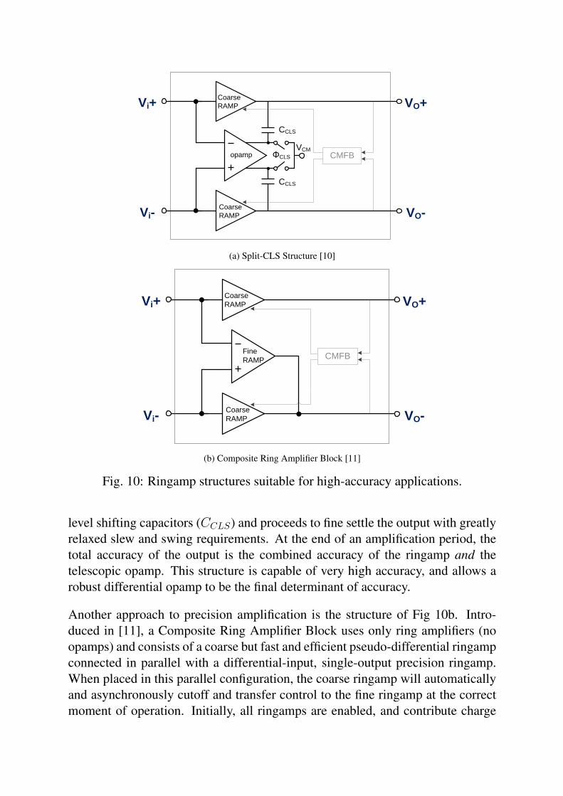
For design scenarios requiring high accuracy amplification, a different approachto ringamp design is required. Fully differential operation is typically mandatory,and the amplifier must either produce very high effective gain or be assisted bycalibration. In [10] the technique of Split-CLS [12] is used to combine a pseudo-differential ringamp structure with a fully differential telescopic opamp. Fig. 10ashows the basic principle of this technique. The ringamps provide an initial fastand coarse charge of the output. Then, the opamp is coupled into the output via the
VO+C-RAMP
VO-RAMP
opamp CMFB
Vi+
Vi-
Coarse
RAMP
Coarse
RAMP
ΦCLS
VCM
CCLS
CCLS
(a) Split-CLS Structure [10]
VO+C-RAMP
VO-RAMP
Fine
RAMPCMFB
Vi+
Vi-
Coarse
RAMP
Coarse
RAMP
(b) Composite Ring Amplifier Block [11]
Fig. 10: Ringamp structures suitable for high-accuracy applications.
level shifting capacitors (CCLS) and proceeds to fine settle the output with greatlyrelaxed slew and swing requirements. At the end of an amplification period, thetotal accuracy of the output is the combined accuracy of the ringamp and thetelescopic opamp. This structure is capable of very high accuracy, and allows arobust differential opamp to be the final determinant of accuracy.
Another approach to precision amplification is the structure of Fig 10b. Intro-duced in [11], a Composite Ring Amplifier Block uses only ring amplifiers (noopamps) and consists of a coarse but fast and efficient pseudo-differential ringampconnected in parallel with a differential-input, single-output precision ringamp.When placed in this parallel configuration, the coarse ringamp will automaticallyand asynchronously cutoff and transfer control to the fine ringamp at the correctmoment of operation. Initially, all ringamps are enabled, and contribute charge
VOUTC2
MCP
MCN
RS
T
RS
T
VCM VCM + VOS
C3
VCM
RS
T
RS
T
VCM - VOS
+VDZ2
-
VIN+ +
-VIN- C1
+
-replica
VCMXVCM
A1 A2
C1B
C2B
C3B
RGC
A3
RS
T
RS
T
SE
T
SE
T
SE
TS
ET
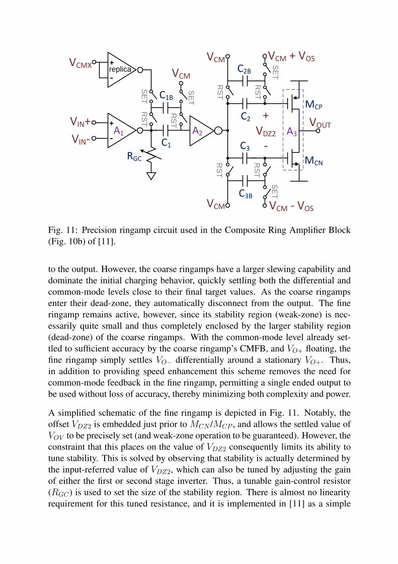
Fig. 11: Precision ringamp circuit used in the Composite Ring Amplifier Block(Fig. 10b) of [11].
to the output. However, the coarse ringamps have a larger slewing capability anddominate the initial charging behavior, quickly settling both the differential andcommon-mode levels close to their final target values. As the coarse ringampsenter their dead-zone, they automatically disconnect from the output. The fineringamp remains active, however, since its stability region (weak-zone) is nec-essarily quite small and thus completely enclosed by the larger stability region(dead-zone) of the coarse ringamps. With the common-mode level already set-tled to sufficient accuracy by the coarse ringamp’s CMFB, and VO+ floating, thefine ringamp simply settles VO− differentially around a stationary VO+. Thus,in addition to providing speed enhancement this scheme removes the need forcommon-mode feedback in the fine ringamp, permitting a single ended output tobe used without loss of accuracy, thereby minimizing both complexity and power.
A simplified schematic of the fine ringamp is depicted in Fig. 11. Notably, theoffset VDZ2 is embedded just prior to MCN /MCP , and allows the settled value ofVOV to be precisely set (and weak-zone operation to be guaranteed). However, theconstraint that this places on the value of VDZ2 consequently limits its ability totune stability. This is solved by observing that stability is actually determined bythe input-referred value of VDZ2, which can also be tuned by adjusting the gainof either the first or second stage inverter. Thus, a tunable gain-control resistor(RGC) is used to set the size of the stability region. There is almost no linearityrequirement for this tuned resistance, and it is implemented in [11] as a simple
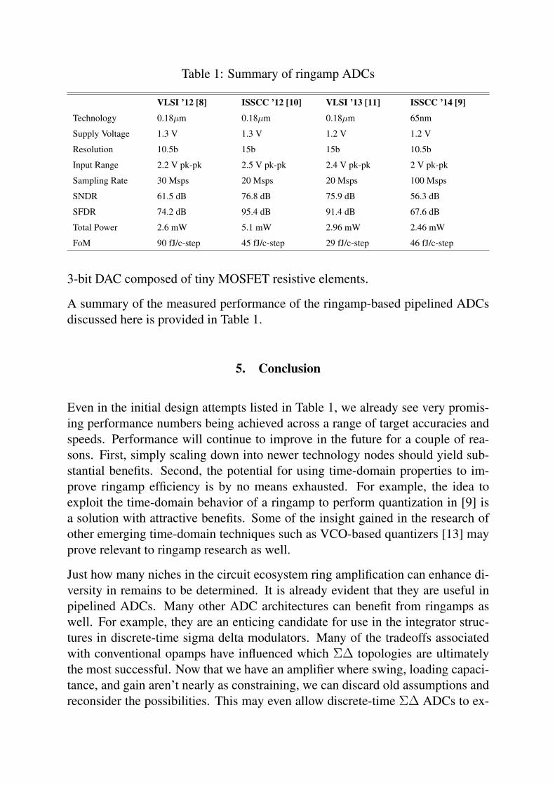
Table 1: Summary of ringamp ADCs
VLSI ’12 [8] ISSCC ’12 [10] VLSI ’13 [11] ISSCC ’14 [9]
Technology 0.18µm 0.18µm 0.18µm 65nm
Supply Voltage 1.3 V 1.3 V 1.2 V 1.2 V
Resolution 10.5b 15b 15b 10.5b
Input Range 2.2 V pk-pk 2.5 V pk-pk 2.4 V pk-pk 2 V pk-pk
Sampling Rate 30 Msps 20 Msps 20 Msps 100 Msps
SNDR 61.5 dB 76.8 dB 75.9 dB 56.3 dB
SFDR 74.2 dB 95.4 dB 91.4 dB 67.6 dB
Total Power 2.6 mW 5.1 mW 2.96 mW 2.46 mW
FoM 90 fJ/c-step 45 fJ/c-step 29 fJ/c-step 46 fJ/c-step
3-bit DAC composed of tiny MOSFET resistive elements.
A summary of the measured performance of the ringamp-based pipelined ADCsdiscussed here is provided in Table 1.
5. Conclusion
Even in the initial design attempts listed in Table 1, we already see very promis-ing performance numbers being achieved across a range of target accuracies andspeeds. Performance will continue to improve in the future for a couple of rea-sons. First, simply scaling down into newer technology nodes should yield sub-stantial benefits. Second, the potential for using time-domain properties to im-prove ringamp efficiency is by no means exhausted. For example, the idea toexploit the time-domain behavior of a ringamp to perform quantization in [9] isa solution with attractive benefits. Some of the insight gained in the research ofother emerging time-domain techniques such as VCO-based quantizers [13] mayprove relevant to ringamp research as well.
Just how many niches in the circuit ecosystem ring amplification can enhance di-versity in remains to be determined. It is already evident that they are useful inpipelined ADCs. Many other ADC architectures can benefit from ringamps aswell. For example, they are an enticing candidate for use in the integrator struc-tures in discrete-time sigma delta modulators. Many of the tradeoffs associatedwith conventional opamps have influenced which Σ∆ topologies are ultimatelythe most successful. Now that we have an amplifier where swing, loading capaci-tance, and gain aren’t nearly as constraining, we can discard old assumptions andreconsider the possibilities. This may even allow discrete-time Σ∆ ADCs to ex-
tend their accuracy and robustness benefits to bandwidths on the order of tens ofmegasamples that are currently achieved only by continuous-time Σ∆ ADCs [2].
There is also much to explore beyond the realm of ADCs. Anything with a capac-itive load is a prime candidate for consideration. This includes switched-capacitorcircuits such as discrete-time filters as well as a variety of sensing and imagingapplications. In all these cases, it is once again useful to re-examine many of theassumptions about what constitutes an “optimal” structure for a given applicationwith specific regard to the strengths and weaknesses of ringamps. In some cases,ringamps may provide the best solution. In other cases, a different technique inthe circuit ecosystem will. This is the strength of circuit diversity.
References
[1] B. Jonsson, “On cmos scaling and a/d-converter performance,” in NORCHIP,2010, nov. 2010, pp. 1 –4.
[2] B. Murmann. (2014) Adc performance survey 1997-2014. [Online].Available: http://www.stanford.edu/ murmann/adcsurvey.html
[3] M. Shrivastava, R. Mehta, S. Gupta, N. Agrawal, M. Baghini, D. Sharma,T. Schulz, K. Arnim, W. Molzer, H. Gossner, and V. Rao, “Toward system onchip (soc) development using finfet technology: Challenges, solutions, pro-cess co-development and optimization guidelines,” Electron Devices, IEEETransactions on, vol. 58, no. 6, pp. 1597 –1607, june 2011.
[4] J. Fiorenza, T. Sepke, P. Holloway, C. Sodini, and H.-S. Lee, “Comparator-based switched-capacitor circuits for scaled cmos technologies,” Solid-StateCircuits, IEEE Journal of, vol. 41, no. 12, pp. 2658 –2668, dec. 2006.
[5] L. Brooks and H.-S. Lee, “A 12b, 50 ms/s, fully differential zero-crossingbased pipelined adc,” Solid-State Circuits, IEEE Journal of, vol. 44, no. 12,pp. 3329 –3343, dec. 2009.
[6] H. Iwai, “Cmos scaling towards its limits,” in Solid-State and IntegratedCircuit Technology, 1998. Proceedings. 1998 5th International Conferenceon, 1998, pp. 31 –34.
[7] B. Hershberg, S. Weaver, K. Sobue, S. Takeuchi, K. Hamashita, andU. Moon, “Ring amplifiers for switched capacitor circuits,” Solid-State Cir-cuits, IEEE Journal of, vol. 47, no. 12, pp. 2928–2942, Dec 2012.
[8] B. Hershberg, S. Weaver, K. Sobue, S. Takeuchi, K. Hamashita, andU. Moon, “A 61.5db sndr pipelined adc using simple highly-scalable ringamplifiers,” in VLSI Circuits (VLSIC), 2012 Symposium on, June 2012, pp.32–33.
[9] Y. Lim and F. P. Flynn, “A 100ms/s, 10.5-bit, 2.46mw comparator-lesspipeline adc using self-biased ring amplifiers,” in Solid-State Circuits Con-ference Digest of Technical Papers (ISSCC), 2014 IEEE International, feb.2014.
[10] B. Hershberg, S. Weaver, K. Sobue, S. Takeuchi, K. Hamashita, andU. Moon, “Ring amplifiers for switched-capacitor circuits,” in Solid-StateCircuits Conference Digest of Technical Papers (ISSCC), 2012 IEEE Inter-national, Feb 2012, pp. 460–462.
[11] B. Hershberg and U. Moon, “A 75.9db-sndr 2.96mw 29fj/conv-stepringamp-only pipelined adc,” in VLSI Circuits (VLSIC), 2013 Symposiumon, June 2013, pp. C94–C95.
[12] B. Hershberg, S. Weaver, and U. Moon, “Design of a split-cls pipelined adcwith full signal swing using an accurate but fractional signal swing opamp,”Solid-State Circuits, IEEE Journal of, vol. 45, no. 12, pp. 2620 –2630, dec.2010.
[13] M. Straayer and M. Perrott, “A 12-bit, 10-mhz bandwidth, continuous-timeΣ∆ adc with a 5-bit, 950-ms/s vco-based quantizer,” Solid-State Circuits,IEEE Journal of, vol. 43, no. 4, pp. 805–814, April 2008.


![RING FAULTS AND RING DIKES AROUND LUNAR BASINS. · gravity [3] data. However, much remains unknown about basin rings, including the properties of the faults, ... the amplification](https://img.pdfslide.us/doc/110x75/5c7b863209d3f2ac4e8b95d3/ring-faults-and-ring-dikes-around-lunar-gravity-3-data-however-much-remains.jpg)