Embed Size (px)
Citation preview
Engineering 1040 Laboratory Exercises
(Electric CircuitsDigital Logic Modules)
Professor Eric W Gill PhD PEng
FALL 2010 Acknowledgements Dr JE Quaicoe for significant parts of the first two labs Dr N Krouglicof for the greater part of the last three labs
Preface
The five laboratory exercises in this manual have been designed to reinforce the concepts encountered in the Electric Circuits and Digital Logic course modules They form a mandatory portion of the course and while they are valued at 5 of the overall mark (10 including the Mechanisms Module(s)) unexcused missed labs will result in an incomplete grade for the course Official documentation such as a doctorrsquos note in the case of illness is required in order to be excused from graded work Documented valid reasons for missing graded work including labs will permit the transfer of the relevant marks to either the midterm or the final examination as agreed to by the instructor and the student
Table of Contents Submission Format and Rules for Lab Reports helliphelliphelliphelliphelliphelliphelliphelliphelliphellip ii Basic Resistive Circuit Parameters 1 Circuit Laws and Troubleshooting helliphelliphelliphelliphelliphelliphelliphelliphelliphelliphelliphelliphelliphelliphelliphellip 14 Application of Resistive Networks helliphelliphelliphelliphelliphelliphelliphelliphelliphelliphelliphelliphelliphelliphelliphellip 26 Introduction to Logic Gates and Ladder Diagrams helliphelliphelliphelliphelliphelliphelliphelliphellip 31 Introduction to Sequential Circuits Ladder Diagrams and Relay Logic 36
ii
Submission Format for Labs Associated with the CircuitsDigital Logic Portions of Engineering 1040
General (1) Use a cover page as shown following these general instructions (2) Start the Prelab immediately after the cover page EACH PERSON in the group must submit a Prelab To obtain full marks for a lab report the Prelabs for all but the first experiment must be shown to the lab Teaching Assistant before the lab starts (3) The name of the person must be attached to the top of each Prelab (4) Label the Prelab sections as they are in the online manual (5) Use only one side of the paper in answering the Prelab questions as well as in the experimental write-up (6) Start the actual lab write-up (one per group) after the last page of the Prelab See the write-up requirements following the sample cover page in this document Put the words ldquoLab Reportrdquo at the top margin of the first page of the actual write-up of the experiment (7) Label the lab report sections as they appear in the online manual (8) Staple the Cover Page Prelabs and Lab Write-up together in a single package (9) Graphs may be done manually or electronically (for example using Microsoft Excel or any other convenient software) (10) Submission of each lab package is required at the start of the subsequent lab
The following four pages elaborate on some of the above points
iii
Sample Cover Page
Faculty of Engineering and Applied Science Memorial University of Newfoundland
Engineering 1040
Lab n
Title Title of Lab as it Appears in the Online Manual
Names Name 1 and Student Number Name 2 and Student Number Date Date that experiment was done
iv
Prelab Name of first person and Student Number At the end of person 1rsquos Prelab on a new page start the second personrsquos Prelab with Prelab Name of second person and Student Number
v
Lab Report Purpose Restate the purpose of the lab as found in the online manual ndash feel free to use your own words Apparatus and Materials List in a column Be sure to give the make and model of the apparatus if applicable For example for the first lab
(1) 2 Fluke 8010A Digital Multimeters (DMM) (2) 1 Sun Equipment Powered Breadboard Model PBB-4060B (3) Standard Resistors 47 Ω 18 Ω 39 Ω 47 Ω 68 Ω 82 Ω 2times100 Ω 150 Ω
330 Ω (4) Two sets of leads with banana plugs and alligator clips (5) Various connecting wires
Theory Give the equations used (along with the meanings of their symbols) For example in Lab 1 part of the theory would be Ohmrsquos Law The voltage (v) current (i) and resistance (R) either for a circuit element or the whole circuit are related as v=iR hellip (1) hellip and so on (for example in Lab 1 you would also give the power formula) Procedure You may simply say ldquoAs per lab manualrdquo Label each part of the Experiment report according to the titles given in the manual Part n Title of this part For example in Lab 1 you would have first Part 41 OHMrsquoS LAW The first sub-heading should be Data Put the labeled circuit diagram (if relevant) at the beginning of this section Under this sub-heading also put (for example)
TABLE 1 - Voltage and Current Measurements for a 994 Ω Resistor Carefully draw the table and fill it in with the measured or calculated values as required Also in the case where table entries require calculations provide sample calculations That is if there are several calculations which have exactly the same form provide a
vi
single sample The other calculations will of course be completed and entered into the table but there is no need to show many calculations which are identical in form The next heading should be (as required) Questions Discussion and Conclusion(s) Label these according to their labels in the manual Repeat the above format for subsequent parts of the experiment For example in Lab 1 the next heading would be Part 42 VOLTAGE AND CURRENT MEASUREMENTS FOR A SIMPLE SERIES CIRCUIT The first sub-heading should be Data Put the labeled circuit diagram (if relevant) at the beginning of this subheading Under this sub-heading also put (for example)
TABLE 2 - Resistance Current and Voltage Measurements Carefully draw the table and fill it in with the measured or calculated values as required Also in the case where table entries require calculations provide sample calculations The next heading should be (as required) Questions Discussion and Conclusion(s) Label these according to their labels in the manual hellip and so on This general approach should be taken in all lab write-ups It may vary slightly depending on the requirements
1
______________________________________________________________________________ E XP 1040-EL1 BASIC RESISTIVE CIRCUIT PARAMETERS PURPOSE
To (i) investigate the relationship between voltage and current in a simple resistive circuit and to (ii) examine the condition for maximum power transfer to a load in such a circuit 10 INTRODUCTION (Note A significant portion of this introduction to the Digital Multimeter is either taken directly or adapted from a Laboratory Manual for the former Engineering 1333 Basic Electrical Concepts and Circuits course prepared by Dr J Quaicoe)
The digital multimeter (DMM) is one of the most versatile general-purpose laboratory instruments capable of measuring dc and ac voltages and currents as well as resistance The quantity being measured is indicated by a numerical display as opposed to a needled deflection on a scale as in analog meters The numerical readout offers the advantages of higher accuracies elimination of parallax reading error or misreading of the scale and increase in the speed of measurements
A typical DMM has three terminals of which one is a COMMON ungrounded terminal (usually black) One of the two terminals (usually red) is the positive reference terminal for current measurements (mA) and the other is the positive reference terminal for voltage and resistance (VkΩs) Several switches are provided to select the measurement mode (ie DC mA DCV ACV etc) and the meter range For this course the DMM which will be commonly used is the Fluke 8010A For this reason the Fluke DMM is discussed in more detail here Figure EL11 shows the front panel features of the Fluke 8010A
Figure EL11 The display for the Fluke 8010A (taken from [1]) Label 9 does not
apply here
The main elements of the meter are as follows (1) An LCD Digital splay
2
(2) ACDC Function Switch (should be OUT for dc and IN for ac measurements)
(3) VmAkΩS Function Switches for measuring voltage current resistance and conductance These are used in combination with (2) depending on whether the circuit is ac or dc The conductance measurements required pushing the kΩ switch along with a pair of conductance range switches
(4) Range Switches for selecting the measurement ranges ndash switch IN means that the range is selected
(5) mA Input Connector ndash this is protected with a 2A fuse Use the red lead in this input
(6) COMMON Input Connector This is the test lead connector used as the lsquolowrsquo or lsquocommonrsquo input for all measurements To keep from being confused use the black lead in this input
(7) VmAkΩS Input Connector This is the test lead connector used for all voltage resistance continuity and conductance measurements Use the red lead in this connector
(8) 10A Input Connector This is used for the 10A Range current function (It wonrsquot be used in this course)
(9) Not available on the 8010A meter (10) Power Switch IN is ON
Before connecting the meter the appropriate measurement mode must be selected
and the meter range set to its highest value
In this experiment the measurement of current voltage and resistance using the DMM is examined 11 Voltage Measurements - The DMM as a Voltmeter
Voltage is measured ACROSS a given element by placing the meter in PARALLEL with the element The positive (red) lead is connected to the assumed positive reference and the negative (black) lead to the assumed negative reference With this connection the meter will read positive if the assumed polarities (ie the + ndash directions) are correct See Figure EL12
All measurements of voltage or potential difference in a circuit require that a reference
point assigned a voltage of zero be established Such a point is known as the REFERENCE NODE and is indicated on a circuit by the ground symbol In our simple circuits it will be assumed to be the same as the node to which the negative terminal of the voltage supply is connected 12 Current Measurements - The DMM as an Ammeter
Current THROUGH an element is measured by placing the meter in SERIES with the element This may require the circuit connection to be broken (open-circuited) and the meter placed in the circuit Power should be OFF when disconnecting any element The meter will read positive when conventional current is flowing into the positive (red) lead See Figure EL13
3
Figure EL12 Voltage measurement with the Fluke 8010A (taken from [1])
Figure EL13 Current measurement with the Fluke 8010A (taken from [1])
13 Resistance Measurements - The DMM as an Ohmmeter
The resistance of a resistor can be measured using the DMM The resistor is connected between the positive voltage lead and the common lead When the kΩ mode is selected the resulting display is a measure of the resistance See Figure EL14
4
Although resistive elements come in many shapes and sizes a large class of resistors fall into the category which is used for circuit components The most common type of resistor is the carbon composition or carbon film resistor Multicolored bands are painted on the resistor body to indicate the standard value of the resistance Figure A1 in the appendix gives the colour codes for carbon composition resistors
Figure EL14 Resistance measurement with the Fluke 8010A (taken from [1])
14 The Accuracy of the Measurements
The accuracy with which the DMM measures each quantity and the frequency range of the input quantity being measured are specified by the manufacturer (usually underneath the meter) These specifications should be examined to determine the accuracy of the reading REFERENCES [1] 8010A8012A Digital Multimeters Instruction Manual John Fluke MFG CO INC 1993 [2] EW Gill Engineering1040 Mechanisms and Electric Circuits Electric Circuits Module 2008
5
20 PRELAB 21 Read Section 1 of EXP 1040-E1L and pages 8-20 of Reference [2] 22 Determine the colour coding for each of the following resistors
i) 47 Ω ii) 18 Ω iii) 47 Ω iv) 100 Ω v) 330 Ω
23 If the resistor in 22 (v) has a lsquogoldrsquo band tolerance determine the range of values which the resistance may take 24 For R lt 200 kΩ the 8010A DMM has a maximum error given by plusmn(02 of the reading + 1 digit) Consider the following example A resistor with colour bands indicating a resistance of 100 Ω and a tolerance of plusmn5 is measured with the DMM and found to have a value of 981 Ω The maximum error is found as follows 981 Ω plusmn (02 of 981 Ω + 1 digit) where one digit now corresponds to 01 Ω Therefore the measurement becomes 981 Ω plusmn (0002 times 981 Ω + 01Ω) = 981 Ω plusmn (02 Ω + 01Ω) = 981 Ω plusmn 03 Ω Note that (0002 times 981 Ω) was rounded to 02 Ω since it is not meaningful to say that the precision of the error is greater than that indicated by the last digit measurable by the device From the point of view of the error the resistance value lies in the range extending from 978 Ω to 984 Ω Notice that this value is well within the tolerance specified (the manufacturerrsquos tolerance of plusmn5 guarantees that the resistance is somewhere between 95 Ω and 105 Ω) Thus using the multimeter and the specified accuracy we have determined a much smaller error on the value of the actual resistance Using the above example determine the error and range of values for a standard value 150 Ω resistor which is measured with the DMM as having a resistance of 148 Ω Does this fall within the gold-band tolerance 23 The components of the circuit of Figure EL15 has the following values vs = 10 V R1 =
100 Ω R2 = 150 Ω Use Kirchhoffrsquos voltage and current laws to find i) the currents through the resistors having the directions shown in the figure ii) the voltages across the resistors having the polarities shown in the figure iii) the power dissipated by each resistor and iv) the power supplied by the source Show that the total power developed in the circuit is equal to the total power dissipated
Figure EL15 A series circuit containing two resistors
6
24 In Figure EL15 determine the equivalent resistance seen by the voltage source ie the input resistance of the circuit given by Rin = vsi1
30 APPARATUS AND MATERIALS
2 Fluke 8010A Digital Multimeters (DMM) 1 Sun Equipment Powered Breadboard Model PBB-4060B Standard Resistors 47 Ω 18 Ω 39 Ω 47 Ω 68 Ω 82 Ω 2times100 Ω 150 Ω 330 Ω Two sets of leads with banana plugs and alligator clips Various connecting wires
40 EXPERIMENT 41 OHMrsquoS LAW Consider the simple circuit shown in Figure EL16
Figure EL16 A simple single-resistor dc circuit
411 Construct the circuit of Figure EL16 on the breadboard using a 100 Ω resistor The A
represents a DMM used as an ammeter and the V represents a DMM used as a voltmeter The latter DMM will be used to measure the resistance before being actually used as a voltmeter DO NOT CONNECT OR TURN ON the voltage source at this stage Measure the value of R using the DMM specified by setting that device on the 200 Ω range (also see the Introduction to the lab) Record the value in the title of Table 1
412 Connect the voltmeter DMM ACROSS R in accordance with the directions given for
voltage measurements specified in the Introduction to the lab That is connect the red lead from the voltmeter to the + side of R shown in the diagram and the black lead to the ndash side of R Set the voltmeter range to 20 V dc Connect the ammeter (DMM) with the red lead on the same node as the black lead for the voltmeter and the black lead on the same node as COM terminal of the powered breadboard Set the ammeter range to 200 mA Connect the red lead from the 0 to 16 V terminal of the breadboard power to the same node as the + side of R NOW turn on the voltage source (powered breadboard) and adjust the supply until the voltmeter (DMM) reads approximately 2 volts
7
413 Record the voltmeter reading and the ammeter reading for the situation in 412 in Table 1 Adjust the power supply to give voltmeter readings of approximately 5 8 11 and 14 volts making sure to read the corresponding ammeter readings Record all voltmeter and corresponding ammeter readings in Table 1
414 From the data of Table 1 plot a graph of voltage versus current and from it determine the
value of R Compare this value with the value of R measured using the DMM in 411 and suggest possible reasons for any discrepancy
TABLE 1 - Voltage and Current Measurements for a _____Ω Resistor
Voltage (V) plusmn(01+1digit)
Current (A) plusmn(03+1digit)
These accuracies for the voltage and currents are found on the bottom of the 8010A 42 VOLTAGE AND CURRENT MEASUREMENTS FOR A SIMPLE SERIES CIRCUIT 421 On the breadboard set up the circuit of Figure EL17 but do not yet connect the voltage
source Resistor R1 is the standard 100 Ω used in part 41 Record its measured value in Table 2 Again using the DMM as an ohmmeter measure the standard 150 Ω resistor and also record its value in Table 2
422 Now connect the voltage source (using the red lead from the 0-16 V to node A and the
Figure EL17 A series circuit with two resistors Note the chosen polarities for the voltages and
the directions for the currents
8
black lead from the COM terminal to node B) Using one of the DMMs as a voltmeter set to read dc volts switch on the source and adjust it to give a reading of +10 V dc on the DMM 423 Measure the voltages across R1 and R2 with the polarities shown Record the readings in Table 2 424 Using the second DMM measure and record in Table 2 the currents through each
resistor taking into account the correct sign as indicated by the directions in Figure EL17
425 Using the measured quantities calculate the power dissipated by each resistor Record
the results in Table 2 426 Compare the measured and standard values of the resistances and the measured and
calculated values of the currents voltages and power Comment on the results 427 Verify that the power delivered by the voltage source is equal to the total power
dissipated by the resistors
TABLE 2 ndash Resistance Current and Voltage Measurements
ParameterVariable Calculated or Standard
(Prelab)
Measured
R1 (Ω)
R2 (Ω)
i1 (mA)
i2 (mA)
vAB (V) v1 (V) v2 (V) P1 (W) P2 (W)
sumPdev (W) sumPdiss (W)
9
43 POWER TRANSFER TO A LOAD RESISTOR Here we use the same circuit set-up as in Figure EL17 but now we will consider that R2
is a load resistor (RL) and we wish to determine the power absorbed by the load for various resistive values while keeping R1 fixed at its measured value found in step 421 Also notice that the polarities have been changed (this is an arbitrary decision) ndash see Figure EL18
Figure EL18 A series circuit containing a single resistor R1 connected to a resistive load RL
431 Using the DMM as an ohmmeter measure the following standard resistors and record the
values in Table 3 47 Ω 18 Ω 39 Ω 47 Ω 68 Ω 82 Ω 100 Ω 150 Ω 330 Ω The 100 Ω resistor is in addition to the one used in part 421 Also you have already measured the 150 Ω resistor and may use its value as found in 421
432 With RL (ie R2) taking the successive measured values of the 47 Ω 18 Ω 39 Ω 47 Ω
68 Ω 82 Ω 100 Ω 150 Ω and 330 Ω resistors use the DMM as a voltmeter to determine the load voltage vL across RL When the 47 Ω and 18 Ω resistors are used for RL it might be useful to set the DMM on the 2 V range For the other resistors use the 20 V range Record all voltage readings in Table 3 433 Using the measured values for vL and RL calculate and record in Table 3 the power absorbed by each load resistor 415 From the data of Table 3 plot a graph of Load Power versus Load Resistance sketch a
smooth curve through the points and from this graph observe and record the value of RL for which the maximum power is absorbed How does this resistance compare with R1 How does the power absorbed by R1 compare with that absorbed by the load resistor when the latter absorbs maximum power
50 CONCLUSIONS State a conclusion for each of the three parts of the experiment
10
TABLE 3 ndash Load Power Measurements
Standard Value of RL (Ω)
Measured Value of RL (Ω)
Load Voltage vL (V)
Load Power PL (W)
47 18 38 47 68 82 100 150 330
11
APPENDIX A (Taken from a Laboratory Manual for the former Engineering 1333 Basic Electrical
Concepts and Circuits course prepared by Dr J Quaicoe) Figure A1 shows the color code for carbon composition resistors along with the procedure for determining the resistance and tolerance from the color codes Table A1 gives a list of readily available standard values of resistors (The Boldface figures are available in the laboratory) If a designer requires other than a standard value such as 38 kΩ then a 39 kΩ resistor will probably be employed since a 38 kΩ resistor falls within the limits of a 39 kΩ resistor with a 10 tolerance
Figure A1 Color code for carbon composition [2] Example Find the resistance value and the tolerance of a resistor having the following color
bands
A - Gray B - Red
C - Black D - Silver
Solution Gray = 8 Red = 2 Black = 0
Silver = plusmn 10
From R = AB Η 10C tolerance = D
R = 82 Η 100 plusmn 10
= 820 Ω plusmn 82 Ω
12
Table A1 Standard Values of Resistors
Ohms (Ω)
Kilohms
(kΩ)
Megohms
(MΩ) 010 10 10 100 1000 011 11 11 110 1100 012 12 12 120 1200 013 13 13 130 1300 015 15 15 150 1500 016 16 16 160 1600 018 18 18 180 1800 020 20 20 200 2000 022 22 22 220 2200 024 24 24 240 2400 027 27 27 270 2700 030 30 30 300 3000 033 33 33 330 3300 036 36 36 360 3600 039 39 39 390 3900 043 43 43 430 4300 047 47 47 470 4700 051 51 51 510 5100 056 56 56 560 5600 062 62 62 620 6200 068 68 68 680 6800 075 75 75 750 7500 082 82 82 820 8200 091 91 91 910 9100
10 100 11 110 12 120 13 130 15 150 16 160 18 180 20 200 22 220 24 240 27 270 30 300 33 330 36 360 39 390 43 430 47 470 51 510 56 560 62 620 68 680 75 750 82 820 91 910
10 100 11 110 12 120 13 130 15 150 16 160 18 180 20 200 22 220 24 27 30 33 36 39 43 47 51 56 62 68 75 82 91
13
Sample Graph
Note the labeling in the following graph which is meant only as an example of how data should be presented graphically Specifically note (1) title (2) name symbol and unit for both the abscissa and ordinate (3) both axes labeled with appropriate scales (4) data points indicated (here small crosses are used) and a best-fit curve drawn through the data points which may or may not lie on the curve itself There are ways of calculating a curve of best-fit but here we simply ldquoguessrdquo how the curve may most accurately be drawn to represent the overall nature of the data In this example our guess is that the curve of best-fit is a straight line
000 003 006 009 012 015
Current i (A)
0
3
6
9
12
15
Vol
tage
v (V
)
Voltage vs Current for a Linear Resistor
14
EXP 1040-EL2 CIRCUIT LAWS AND TROUBLESHOOTING PURPOSE
To (i) further verify the validity of the basic circuit laws ie Ohms law and Kirchhoffs Laws when applied to a resistive circuit and (ii) briefly examine some simple ideas associated with troubleshooting a circuit 10 INTRODUCTION
Circuit analysis is the process by which all voltages and currents associated with each element in a given circuit are evaluated Conversely circuit synthesis (or circuit design) involves determining the necessary circuit element values and their interconnection in order to achieve desired voltages and currents Two simple but sufficient laws form the basis for electric circuit analysis and synthesis The first of these describes the characteristics or properties of a particular element irrespective of how it is connected to other elements in a circuit It is often expressed in terms of the current THROUGH and voltage ACROSS the element ie the i-v characteristics of the element and is named Ohms law The second is a network law that applies to the interconnection of elements rather than to individual elements The law describes the inherent constraints on voltage and current variables by virtue of interconnections and is expressed in Kirchhoffs laws which really follow from the conservation of energy and continuity of current (or conservation of charge) principle
In this experiment the basic laws are examined by investigating the behaviour of a simple circuit 11 Ohms Law
Ohms Law is based on a linear relationship between voltage and current Ohms Law states that the voltage across many types of conducting materials is directly proportional to the current flowing through the material It is expressed mathematically as v = Ri 11 where the constant of proportionality R is called the RESISTANCE A resistance for which the voltage versus current relationship is a straight line is a LINEAR RESISTANCE A linear resistance obeys Ohms Law because the resistance is always constant However a resistance whose ohmic value does not remain constant is defined as a NONLINEAR RESISTANCE Many resistors lose their linearity as the operating conditions (eg temperature) changes 12 The Electric Circuit
An electric circuit consists of circuit elements such as energy sources and resistors connected by electrical conductors or leads to form a closed path or combination of paths through which current can flow A point at which two or more elements have a common connection is called a NODE A two-terminal circuit element connected between two nodes is called a BRANCH A branch may contain more than one element between the same nodes
15
When two or more circuit elements are connected together an ELECTRIC NETWORK is formed If the network contains at least one closed path the network is called an ELECTRIC CIRCUIT 13 Kirchhoffs Laws 131 Kirchhoffs Current Law (KCL)
Kirchhoffs current law describes current relations at any node in a lumped network It states that the algebraic sum of the currents entering (or leaving) any node or cutset (supernode) is zero (The idea of a supernode is not part of this course) Kirchhoffs current law relates to the conservation of charge since a node cannot store destroy or generate charge It follows that the charge flowing out of a node exactly equals the charge flowing into the node An equivalent way of saying this is to say that the current at a node is continuous 132 Kirchhoffs Voltage Law (KVL)
Kirchhoffs voltage law describes voltage relations in any closed path in a lumped network It states that the algebraic sum of the voltages around any closed path is zero Kirchhoffs voltage law expresses the principle of conservation of energy in terms of the voltages around a closed path Thus the energy lost by a charge travelling around a closed path is equal to the energy gain 14 Voltage Notations
It is usual to express all potentials in a circuit with respect to a reference point (assumed to have zero potential) For example the potential of point A or the voltage of point A with respect to some reference point is indicated as vA The potential of a point with respect to a second point other than the reference point is indicated by a double subscript For example in Figure EL21 the potential of A with respect to B is indicated as vAB The second subscript indicates the reference point Thus the potential of B with respect to A is represented by vBA
Figure EL21 Voltage notation Note that vBA = ndash vAB REFERENCES [1] The Introduction and Appendix A of laboratory exercise EXP 1040-EL1 [2] EW Gill Engineering1040 Mechanisms and Electric Circuits Electric Circuits Module 2008 [3] S Wolf and R Smith Electronic Instrumentation Laboratories Prentice-Hall NJ 1990
16
20 PRELAB 21 Read Section 1 of EXP 1040-EL1 and pages 13ndash26 of Reference [2] 22 Determine the colour coding for each of the following resistors
i) 820 kΩ ii) 1 kΩ iii) 68 MΩ iv) 18 MΩ 23 Consider the circuit of Figure EL22
i) Write the Kirchhoffrsquos voltage law equations for loops adba and adcba ii) Write the Kirchhoffrsquos current law equations for nodes d and c iii) Use the four equations in (i) and (ii) to find the currents i1 i2 i3 and i4 iv) Find the voltages across the resistors having the polarities shown in the figure v) Determine the power dissipated by each resistor vi) Find the power supplied by the source and compare with the total power
developed in the circuit 24 In Figure EL22 determine the equivalent resistance seen by the voltage source ie the
input resistance of the circuit given by Rin = vABi1 25 Troubleshooting is the process of identifying and locating a failure (fault) or problem in a
circuit Generally the problems are due to open circuits or short circuits Consider the circuit of Figure EL22 A DMM set to measure the voltage across R4 reads vCB = 228 V Determine if there is a fault in the circuit If there is a fault identify it as either a short or open circuit
30 APPARATUS AND MATERIALS
1 Fluke 8010A Digital Multimeter (DMM) 1 Sun Equipment Powered Breadboard Model PBB-4060B Standard Resistors 2times100 Ω 150 Ω 220 Ω One set of leads with banana plugs and alligator clips Various connecting wires
40 EXPERIMENT 41 RESISTANCE MEASUREMENT USING THE DMM 411 With the DMM set to measure RESISTANCE measure and record in Table 1 the
resistance of each resistor in the circuit of Figure EL22 Note that the resistance of each resistor must be measured separately Also record the standard values
412 Construct the circuit of Figure EL22 on the breadboard provided Do not connect the
voltage source to the circuit With the DMM set to read RESISTANCE connect the DMM to nodes a and b and record the equivalent resistance of the resistive circuit as Rin in Table 1 Also record in Table 1 Rin calculated using the values measured in 411
17
vab = +8 V R1 = 100 Ω R2 = 220 Ω R3 = 150 Ω R4 = 100 Ω
Figure EL22 Series-parallel circuit for analysis and experimentation
42 VOLTAGE AND CURRENT MEASUREMENTS USING THE DMM 421 Connect the voltage source to the resistive circuit at points a (red lead) and b (black lead)
Set the DMM to read dc volts and adjust the 0 to 16 V voltage source from the breadboard to give a +8 V dc reading on the DMM Record this as vab in Table 1 Note It may not be possible to adjust the source to read exactly +8 V ndash simply record the closest value that you are able to obtain
422 Recall the voltage measurement technique from the information given in Lab 1 Measure and record in Table 1 the dc voltages across the resistors in the circuit of Figure EL22
with the polarities as specified Set the DMM on the most appropriate range for these measurements
423 Recall the current measurement technique from the information given in Lab 1 With the
DMM set on dc amps measure the current flowing in each resistor with the directions specified in Figure EL22 Record the results in the Table 1
424 Using the measured quantities calculate the power dissipated by each resistor Record
the results in Table 1 425 Compare the measured (or lsquostandardrsquo in case of the resistors) and calculated results of the
resistances currents voltages and power Comment on the results 426 From the results for the measured voltages in Table 1 verify that (within expected errors)
KVL has been satisfied for (i) mesh adba (ii) loop adcba and (iii) mesh dcbd Briefly discuss any discrepancy Note a mesh is a loop that does not contain any other loop(s) For example in this circuit loop adcba contains mesh adba and mesh dcbd
18
427 From the results for the measured currents in Table 1 verify that (within expected errors) KCL has been satisfied for (i) node d and (ii) node c Briefly discuss any discrepancy
428 Verify that the power delivered by the voltage source is equal to the total power
dissipated by the resistors 43 TROUBLESHOOTING 431 Verify the troubleshooting problem in Section 25 432 Provide an analysis of the problem and discuss the conceptual basis for identifying the
type of fault 50 CONCLUSIONS
19
TABLE 1 ndash Resistance Current and Voltage Measurements
ParameterVariable
Standard or Calculated
Measured
R1 (Ω)
R2 (Ω)
R3 (Ω)
R4 (Ω)
Rin (Ω)
vab (V)
v1 (V)
v2 (V)
v3 (V)
v4 (V)
i1 (mA)
i2 (mA)
i3 (mA)
i4 (mA)
P1 (W)
P2 (W)
P3 (W)
P4 (W)
Pdev (W)
Pdiss (W)
20
APPENDIX A (Modified from the former Engineering 1333 Lab manual by Dr John Quaicoe)
This appendix contains several important ideas that will be useful in any of your encounters with real electric circuits In reality measurements in a circuit will depend on all elements of the circuit and all connectors as well as on the operating conditions A1 Resistors
The flow of charge through any material encounters an opposing force This opposition due to the collisions between electrons and between electrons and other atoms in the material which converts electrical energy into heat is called the resistance of the material A device specifically designed to have resistance is called a resistor A11 Factors Which Affect Resistance
The resistance of any material with a uniform cross sectional area depends on the material used the length the cross-sectional area and temperature under which operation occurs Conductor Length and Cross Sectional Area
If the effects of temperature are neglected resistance depends directly on the length of the material and inversely on the cross-sectional area In equation form the resistance of a conductor at room temperature of 20oC is expressed as R = ρlA (A1) where R is the resistance in ohms
l is the length in metres or feet A is the cross-sectional area in m2 or circular mils (CM) ρ is the resistivity or specific resistance in Ωmiddotm or ΩmiddotCMft
Electrical conductors are generally circular in cross-section with wire diameters measured
in mils 1 mil = 11000 in = 10-3 in (A2) The cross-sectional area of a conductor is for convenience defined in circular mils The circular mil is the area of a circular cross-section having a diameter of 1 mil Area (circle) = πd24 (A3) Since the area depends on the square of the diameter for any arbitrary diameter d in mils the area in circular mils is given by A = d2 cir mils (CM) (A4)
It is still quite common to define the resistivity in the Imperial (English) system as the resistance of a 1 ft length of conductor with an area of 1 CM Of course the SI unit for
21
resistivity as is easily deduced from equation (A1) will be the Ωmiddotm Table A1 lists resistivity values of common conducting materials in both SI and Imperial units
Table A1 The resistivities of common conducting materials at 20oC
Conducting Material
Resistivity (Ωm)
Resistivity (Ωcir milft)
Aluminum
283 x 10-8
170
Brass
7 x 10⁻⁸
420
Copper annealed
172 x 10-8
1037
Copper hard-drawn
178 x 10-8
107
Gold
245 x 10-8
147
Lead
221 x 10-8
132
Nichrome
100 x 10-8
600
Platinum
10 x 10-8
602
Silver
164 x 10-8
99
Tin
115 x 10-8
692
Tungsten
552 x 10-8
332
Zinc
623 x 10-8
374
Examples 1 An annealed copper bar measures 1 x 3 cm and is 12 m long What is the resistance
between the ends of the bar
Solution R = ρlA = (172 x 10-8) x (5 x 10-1)(1 x 10-2 x 3 x 10-2)
= 285 x 10-5 Ω
2 Find the resistance of an annealed copper wire 200 ft long with a 100 mil diameter
Solution A(cir mil) = d2 = (100)2 = 104 CM R = ρlA = (1037) x (200)104 = 207 x 10ndash2 Ω
22
Temperature Effects
For most conductors as the temperature increases either from current flowing through it or by heat absorption from the surrounding medium the resistance increases This is due to the increased molecular movement within the conductor which hinders the flow of charge The resistance increases almost linearly with increase in temperature
The relationship between temperature and resistance is expressed as (|T| + t1)R1 = (|T| +t2)R2 (A5) where |T| is the inferred absolute zero of the material involved in oC R1 is the resistance of the material at the temperature t1
oC R2 is the resistance of the material at the temperature t2
oC
The relationship between temperature and resistance may be expressed by
R2 = R1 [1 + α1(t2 - t1)] (A6) where α1 is the temperature coefficient of resistance
R1 is the resistance at the temperature t1 and
R2 is the resistance at the temperature t2
Table A2 lists the inferred absolute zero and temperature coefficients of common conducting materials
Most materials exhibit an increase in resistance with an increase of temperature and are said to have a positive temperature coefficient of resistance However some materials such as carbon and semiconductor materials exhibit a decrease in resistance with an increase of temperature and are said to have a negative temperature coefficient of resistance Examples 1 What is the resistance of an annealed copper wire at 10oC if the resistance is 50 Ω at
60oC
Solution (|T| + t1)R1 = (|T| +t2)R2 t2 = 60o R2 = 50 Ω |T| = 2345o
t1 = 10oC R1 =
R1 = (|T| + t1) R2 (|T| + t2)
= 50 x (2445)(2945) = 415 Ω
23
2 What is the resistance of a copper wire at 10oC if the resistance at 20oC is 433 Ω and if
α1 = 000393
Solution
R2 = R1(1 + α1 ΔT)
= 433 [1 + 000393 (10-20)] = 416 Ω
Table A2 Inferred absolute zero and temperature coefficients for common conducting materials
Conducting
Material
Inferred Absolute zero (C)
Temperature coefficient (Ω CΩ at 0oC)
Aluminum
-236
000424
Brass
-480
000208
Copper annealed
-2345
000427
Copper hard drawn
-242
000413
Gold
-274
000365
Lead
-224
000466
Nichrome
-2270
000044
Platinum
-310
000323
Silver
-243
000412
Tin
-218
000458
Tungsten
-202
000495
Zinc
-250
000400
24
A1 2 Wire Tables [3] Circular cross-section wire is designed by a gauge size of number representing a certain diameter wire The wire table is designed primarily to standardize the size of wire produced by manufacturers The American Wire Gauge (AWG) sizes are given in Table A3 Note that the larger the gauge number the smaller the diameter of the conductor
Table A3 American Wire Gauge (AWG) Sizes of Copper Wire [3]
APPLICATIONS
AWG
AREA (CM)
Ω1000 ft (200 C)
Max Current
(900 C) Power distribution
00
133100
0078
186
1
83690
0124
137
4
41470
0240
89
House main power carriers
6
26240
0395
65
8
16510
0620
48
Lighting outlets general home use
12
6530
1588
20
14
4110
252
15
Television radio
20
10215
101
-
22
6424
161
-
Telephone instruments
28
1598
649
-
35
315
3290
-
40
99
10490
-
An examination of the table shows that if the gauge number changes by 10 the cross-
sectional area changes by approximately a factor of 10 Thus the resistance also changes by approximately 10 times For example AWG 4 has a cross-sectional area of 41470 CM and resistance of 0240 Ω1000 ft whereas AWG 14 has a cross-sectional area of 4110 CM and a resistance of 252 Ω1000 ft ie an increase of 10 in the gauge number represents a decrease in the area by a factor of approximately 10 and an increase in the resistance by a factor of approximately 10 A13 Types of Resistors
Resistors are used for many purposes and are therefore made in many forms The most common of the resistor types are the carbon composition resistor the wirewound resistor the
25
metal film resistor and the carbon film resistor They all belong in either of two groups fixed or variable
The most common of the low-wattage fixed-type resistors is the carbon composition resistor It is made of hot-pressed carbon granules mixed with varying amounts of binding material to achieve a large range of resistance values They are used extensively in electronic applications They are relatively inexpensive reliable and free of stray capacitance and inductance They are available in power ratings up to 2W with resistance values in the range of 1 to 22 MΩ and 5 to 20 tolerance The resistance value of carbon composition resistors and tolerances are specified by a set of colour-coded bands painted on the resistor body Each colour represents a digit in accordance with Figure A1 in the appendix of Exp 1040-EL1 The resistance value as indicated by the colour bands of carbon composition resistors is called the nominal value of resistance Wire wound resistors are commercially available for high precision low resistance and high power dissipation applications They usually consist of Nichrome or copper-nickel wire wound on a ceramic tube and protected from mechanical and environmental hazards by a protective coating of vitreous enamel or silicone Their resistance values range from 1Ω to 100 kΩ with a tolerance range of 00005 and above and a maximum power rating of 200 W
A third group of resistors consist of a thin film of material deposited on insulating materials to provide very high resistance paths Depending on the material used the resistors are classified as carbon film metal film or metal-oxide film resistors Their values range up to 10000 MΩ
Variable resistors come in many forms but basically they can be separated into the linear or non-linear types Variable resistors usually have three leads two fixed and one moveable If contacts are made to only two leads of the resistor the variable resistor is being employed as a rheostat If all three contacts are used in a circuit it is termed as potentiometer or pot The value of the overall resistance and the power ratings of variable resistors are usually stamped on their cases Because the resistance of a conducting film varies with length cross-section and temperature it is possible to use resistance measurement to sense changes in any of those parameters A device that responds to one physical effect is called a transducer Electrical transducers are often used in instrumentation for non-electrical quantities such as temperature light and strain The resistance of the device can be measured and the magnitude of the physical or chemical parameter inferred from the resistance value Typical examples of resistive transducers are 1 The thermistor a two-terminal semiconductor device designed specifically to exhibit a
change in electrical resistance with a change in its body temperature 2 The strain gauge a device which converts linear dimension changes into resistive
changes 3 The photoconductive cell a two-terminal device whose resistance depends upon the
intensity of light impinging on the cell
EXP 1040-EL3 Applications of Resistive Networks PURPOSE To (1) investigate the idea of voltage division using a single source and (2) to examine the utility of a Wheatstone bridge circuit for resistance measurements 10 INTRODUCTION
Using the laws discussed in the course material ndash namely Ohmrsquos law Kirchhoffrsquos Voltage Law (KVL) and Kirchhoffrsquos Current Law (KCL) ndash we are now in a position to study many different circuits having a variety of real-world applications In this lab we consider two such applications and while the analysis associated with them is relatively straight forward they are of significant modern-day importance 11 Voltage Divider Circuits
A voltage source is sometimes required to supply a particular voltage to a load and in fact it may be required to supply several loads with certain specified voltages simultaneously Ideally the voltage supplied should not depend on the size of the load
As a first example consider the circuit shown in Figure EL31 in which a simple voltage
divider circuit is connected in series with the load Notice the situation has been depicted in two equivalent ways In the second schematic the negative terminal of the source is assumed to be electrical ground An electrical ground is a reference level from which other voltages are measured An ideal electrical ground can absorb an unlimited amount of current without changing its potential Here then conventional current flows from the positive terminal of the source through the resistors and back to the source via the ground path (the closed path connection is not explicit in the schematic diagram but it is understood)
Figure EL31 Two equivalent schematics (a) and (b) for a simple voltage divider
From Section E251 of the class notes Electric Circuits Module we know that
⎥⎦
⎤⎢⎣
⎡+
=Ls
LsL RR
Rvv (1)
26
However this type of voltage divider has a serious disadvantage since the value of vL depends on the value of iL and the latter will change depending on the value of the load resistance
To help overcome the problem referred to above it is possible to construct a voltage divider with a bleeder resistor RB as shown below in Figure EL32 and as discussed in Section 251 (page 29) of the class notes Electric Circuits Module
Figure EL32 Two representations (a) and (b) of a voltage divider with a bleeder resistor Strictly the voltage across the parallel section of the circuit is (by the voltage divide lsquorulersquo)
⎥⎦
⎤⎢⎣
⎡+
=)||(
||
BS
LBsL
LRRRRRvv (2)
where
⎥⎦
⎤⎢⎣
⎡+
=LRR
RRRRB
LBLB || (3)
As shown in the class notes the advantage of this kind of voltage division is that when RBltltRL the load voltage is essentially independent of the load resistance and
⎥⎦
⎤⎢⎣
⎡+
=BS
BsL RR
Rvv (4)
Because the load voltage is less affected by the load resistance in this situation we say there is better voltage regulation in this circuit than that in Figure EL31 12 The Wheatstone Bridge The Wheatstone bridge circuit is mainly used to measure an unknown resistance However the principle of the Wheatstone bridge is used in many transducers ndash devices that convert one kind of energy into another ndash and instrumentation systems to measure a physical variable such as 27
strain temperature and pressure A Wheatstone bridge circuit is shown in Figure EL33 In this figure R3 is a variable resistance which models the transducer If a change in physical variable results in a change in resistance of the transducer the Wheatstone bridge can be used to convert the change in resistance to a change in voltage which can be measured
Figure EL33 A Wheatstone bridge
When the voltage vab is zero the bridge is said to be balanced If two resistances (say R1 and R2) are known and another (say Rx) is unknown then a fourth adjustable known resistance R3 (potentiometer) can be used to determine the unknown resistance Rx under balanced conditions When R3 is actually a transducer whose resistance changes with some change in a physical parameter such as temperature then if R1 R2 and Rx are known the voltage vab is an indicator of the size of the measured parameter Balanced Conditions As noted for balanced conditions the voltage vab is zero Also under these conditions using the voltage divide rule twice gives
⎥⎦
⎤⎢⎣
⎡+
=x1
x
RRRvvad (5)
⎥⎦
⎤⎢⎣
⎡+
=32
3
RRRvvbd (6)
We have also seen from Section 254 of the Electric Circuits Module lecture notes that
32
1x R
RRR ⎟⎟
⎠
⎞⎜⎜⎝
⎛= (7)
Unbalanced Conditions When the bridge is not balanced ndash ie vab ne 0 ndash then using Kirchhoffrsquos laws it is straight forward to show that
⎥⎦
⎤⎢⎣
⎡+
minus+
=32
3
x1
x
RRR
RRRvvab (8)
28
29
From this equation we see immediately that if any three of the resistances are fixed in value then a change in the other resistance results in a change in vab Thus a variation in vab is effectively a measure of a change in the variable resistance REFERENCES [1] The Introduction and Appendix A of laboratory exercise EXP 1040-EL1 [2] EW Gill Engineering1040 Mechanisms and Electric Circuits Electric Circuits Module 2008 20 PRELAB 21 Carefully read Section 1 (Introduction) of this experiment and the sections referred to in reference [2] 22 Refer to Figure EL31 The series dropping resistor has a value of 10 kΩ (a) Determine the value of the load resistor RL so that vL = 75 V if the source voltage is 10 V (b) If the load resistance is increased by 25 calculate the new vL 23 Refer to Figure EL32 (a) Design a voltage divider (ie find Rs and RB) for the load
resistance RL obtained in part (a) of Question 22 so that it can operate at vL = 75 V from a 10 V source Assume that the bleeder current iB is 75 mA (b) If the load resistance is increased by 25 calculate the new load voltage Compare this result with that obtained in Question 22 (b) Comment on the comparison
30 APPARATUS AND MATERIALS
1 Fluke 8010A Digital Multimeter (DMM) 1 Sun Equipment Powered Breadboard Model PBB-4060B Standard Resistors 1 kΩ 3 times 120 Ω others as calculated in design Potentiometers 200 Ω 5 k Ω One set of leads with banana plugs and alligator clips and various connecting wires
40 EXPERIMENT 41 Voltage Divider 411 Familiarize yourself with potentiometers ndash the lab attendants will help On the breadboard construct the voltage divider circuit as shown in Figure EL31 using a 1 kΩ resistor for Rs and a 5 k Ω potentiometer (variable resistor) as the load resistor RL Ensure that the source voltage is 10 V after connecting to the circuit Adjust the variable resistor to get an output (load) voltage of vL = 75 V Measure the value of RL for this condition Comment on any discrepancies between the measured and calculated value in Question (22) of the Prelab
30
412 Vary the potentiometer resistance from 680 Ω to 5 k Ω and obtain the load voltage vL in each case Tabulate your results and plot vL as a function of RL 413 Construct the voltage divider found in Figure EL32 and measure the load voltages to
verify your design of Question 23 of the Prelab Use the nearest available resistance values to those you calculated in the design Comment on your findings
42 Wheatstone Bridge 421 On the breadboard construct the Wheatstone bridge circuit of Figure EL33 using three
120 Ω (nominal) resistors for R1 R2 and Rx and a 200 Ω potentiometer (pot) for R3 Also measure and record the actual values of the 120 Ω resistors Ensure that the source voltage v is 10 V after it is connected to the circuit Use the DMM as a voltmeter in the branch between nodes a and b
422 Adjust the pot until the bridge is balanced Measure and record the value of R3 for this
condition Confirm your observation by calculating R3 from equation (7) and comment on any discrepancies
50 DISCUSSION 51 Comment on probable applications of a voltage divider circuit 52 Discuss any technical difficulties encountered during the lab
_____________________________________________________________________________ EXP 1040-DL1 Introduction to Logic Gates and Ladder Diagrams PURPOSE To (i) familiarize the student with the basic logic gates AND OR NOT and NAND (ii) implement basic logic gates using relay logic and (iii) learn how to represent logic circuits by means of ladder diagrams 10 INTRODUCTION Logic circuits may be implemented (constructed) in a variety of ways perhaps most commonly today via electronic components In this lab and the next however we consider the implementation of basic logic expressions using a simple circuit board in conjunction with a few pneumatic cylinders This allows us to explore basic logic circuits without having to resort to sophisticated solid state circuitry (transistors etc) 20 PRELAB There is no prelab for this session However students need to read Section D13 pages 10-18 of the Digital Logic Module before the lab session 30 APPARATUS AND MATERIALS 1 Logic Board Various banana plug connectors AC power (from main lab supply) 40 EXPERIMENT
41 Board Familiarization 411 Normally-open Switch To gain familiarity with the laboratory test panel implement the simple circuit shown in Figure DL11 PB1 refers to one of the two push buttons available on the panel This specific circuit utilizes a ldquonormally openrdquo contact When PB1 is pressed the green indicator light should illuminate
31
CGreenPB1
24V N
Figure DL11 Simple circuit employing push button and a green indicator light
412 Normally-closed Switch Repeat exercise 411 using the ldquonormally closedrdquo contact of PB1 See Figure DL12
CGreen
24V N
PB1
Figure DL12 Simple circuit employing a normally closed contact
42 AND Gate
Using the two push buttons PB1 and PB2 implement an AND operation In other words the green indicator light should only illuminate if and only if both buttons are pressed simultaneously In your lab report provide
bull the ladder diagram implementation (similar to Figure DL11 or DL12) bull the standard symbol for a two input AND gate bull The truth table Note that the truth table should include all four combinations
of the two inputs Assume that a high or logic ldquo1rdquo occurs when the button is pressed
bull Provide a practical application of this circuit (hint think safety)
32
43 OR Gate
Repeat part 42 above in its entirety however this time implement an OR operation using the two push buttons PB1 and PB2 In this case the green indicator should illuminate if at least one of the two buttons is pressed For the practical application consider convenience instead of safety
44 OR Gate
Repeat part 42 above for a ldquoNANDrdquo gate Note that this will require normally closed contacts It is not necessary to provide a practical application for this circuit
45 NOR Gate
Repeat part 42 above for a NOR gate Note that this will require normally closed contacts It is not necessary to provide a practical application for this circuit
46 Inequality Comparator Figure DL13 represents a circuit that is sometimes referred to as an inequality comparator Implement the circuit and experimentally determine the truth table Note that this circuit employs both the ldquonormally openedrdquo and ldquonormally closedrdquo contacts of both push buttons In the lab report provide both the common name for this circuit as well as the standard logic symbol Why is this circuit referred to as an ldquoinequality comparatorrdquo
CGreen
24V N
PB1 PB2
PB_2PB_1
Figure DL13 Circuit that implements an ldquoinequality comparatorrdquo
47 Inverter
An inverter or NOT gate can be implemented with a relay as shown in Figure DL14 When the push button is pressed the coil of relay 1 is energized This opens the normally closed contact of relay 1 which turns the Green indicator light off Implement the circuit and experimentally determine the operation In the lab report provide the standard logic symbol for a NOT gate
33
CR1
24V N
PB2
R_1C
Green
Figure DL14 Circuit that implements a NOT gate
48 Latch (Priority on Set)
A relay can also be used to ldquolatchrdquo the state of the output such that the indicator light is illuminated when the push button is pressed and stays illuminated even if the button is released A second push button must be used to reset the circuit back to its initial (ldquoOFFrdquo) state In Figure DL15 PB1 energizes relay 1 when it is pressed One of the sets of contacts on relay 1 is used to maintain the relay energized even if PB1 is released The normally closed contact of button PB2 de-energizes the relay when the button is pressed (ie resets the latch) Implement the circuit and experimentally determine the operation Be sure and verify what happens when both buttons are pressed simultaneously Note that you must use a different set of relay contacts to energize the green indicator light This particular latching configuration is referred to as priority on SET
CR1
24V N
PB1
PB2
CGreen
R_1
R__1
Figure DL15 Implementation of a ldquolatchrdquo circuit using a relay
34
49 Latch (Priority on Re-Set)
An alternative latch configuration is implemented in Figure DL16 This configuration is referred to as priority on RESET Implement the circuit and experimentally determine the operation Be sure and verify what happens when both buttons are pressed simultaneously In terms of operation what is the main difference between ldquopriority on SETrdquo and ldquopriority on RESETrdquo Provide a practical application of both latch configurations (once again think safety)
CR1
24V N
PB1 PB2
CGreen
R_1
R__1
Figure DL16 Implementation of ldquopriority on RESETrdquo
35
_____________________________________________________________________________ EXP 1040-DL1 Introduction to Sequential Circuits Ladder Diagrams and Relay Logic PURPOSE To (i) introduce ladder diagrams and relay logic and (ii) demonstrate a simple pneumatic system 10 INTRODUCTION Ladder Diagrams (Figure DL21) are a graphical representation of sequential control circuits that are widely used in industry Although originally intended as a way of representing relay logic ladder diagrams are now the standard means of programming microprocessor based PLCs (Programmable Logic Controllers) They are prevalent in a many engineering fields including automation process control and manufacturing In this lab a sequential logic circuit will be implemented using the pneumatic test board The pneumatic test board has three pneumatic cylinders that are activated by solenoid valves The position of each cylinder is monitored by two limit switches One limit switch is activated when the cylinder is fully extended and the other is activated when the cylinder is fully retracted By energizing a solenoid you are able to extend a cylinder and by de-energizing the solenoid the cylinder will retract 20 PRELAB There is no prelab for this session However students need to read Unit D2 of the Digital Logic Module before the lab session 30 APPARATUS AND MATERIALS 1 Logic Board Various banana plug connectors AC power (from main lab supply) Compressed air source 40 EXPERIMENT
41 Limit Switch Familiarization
36
Limit switches A0 and A1 in Figure DL21 are used to sense when cylinder A is retracted and extended respectively Each switch incorporates both a normally opened and normally closed set of contacts Cylinders B and C employ switched B0 B1 and C0C1 respectively These six switches are identified on the wiring panel as S1 through S6 An indicator light can be used to verify the operation of the switches Sketch a circuit that illuminates the green light when cylinder A extends and the red light when cylinder A retracts Implement the circuit on the pneumatic test board and verify the operation by manually depressing the limit switches Use the circuit to determine the correspondence between the six limit switches and the wiring terminals S1 through S6
Figure DL21 Ladder diagram (left) for controlling two pneumatic cylinders 42 Solenoid Valve Familiarization
Solenoid valves S1 S2 and S3 control the three cylinders A B and C As shown in Figure DL21 when the solenoid valves are not energized the cylinders are retracted ie pressure is applied to the rod side of the cylinder Energizing the solenoid changes the position of the valve such that the cap side of the cylinder is pressurized and the
37
38
cylinder extends Sketch a circuit that extends cylinder A when push button PB1 is depressed and retracts A when the button is released Implement the circuit on the pneumatic test board and verify the operation There are a many ldquopinchrdquo points on the test board so be sure and keep your fingers away from the cylinders
43 Implementation of a Simple Latch
Using relay 1 design a circuit that latches the state of push button PB1 such that cylinder A extends when PB1 is depressed and stays extended even if PB1 is released The cylinder retracts only when push button PB2 is depressed Implement the circuit on the pneumatic test board and verify the operation
44 Sequential Logic Circuit 1 441 Familiarization with the Logic Sequence
The ladder diagram shown in Figure DL21 is a sequential logic circuit that will make two cylinders follow the sequence Cylinder A ndash extend -gt Cylinder B ndash extend -gt Cylinder A ndash retract -gt Cylinder B ndash retract The operation of the logic circuit can be described as follows
bull Push button PB1 initiates the start of the sequence ie extend cylinder A by activating solenoid A Relay 2 is latched when PB1 is depressed if and only if the last step in the sequence (limit switch B0 retract B) has been completed This also maintains solenoid A energized bull Once cylinder A has finished extending (ie switch A1 is active) the circuit advances to the second ldquorungrdquo of the ladder which activates solenoid B (cylinder B extends) bull When switch B1 is activated (ie B extended) the circuit advances to the third rung in the ladder Relay 4 is latched which in turn resets relay 2 de-energizing Solenoid A and retracting A bull In a similar fashion the fourth rung in the ladder resets relay 3 which retracts B bull Notice that each rung in the ladder is latched by the completion of the action associated with the previous rung
442 Implementation of the Logic Sequence
Implement the circuit described in 441 and verify the operation
45 Sequential Logic Circuit 2
Modify the circuit in section 44 to implement the following sequence
39
Cylinder A ndash extend -gt Cylinder B ndash extend -gt Cylinder B ndash retract -gt Cylinder A ndash retract
5 Lab Report 51 Provide a short written lab report that includes ladder diagrams of all the circuits design during the lab
52 Explain the operation of the circuit developed in part 45 above
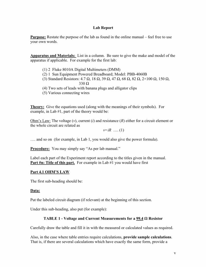

1
______________________________________________________________________________ E XP 1040-EL1 BASIC RESISTIVE CIRCUIT PARAMETERS PURPOSE
To (i) investigate the relationship between voltage and current in a simple resistive circuit and to (ii) examine the condition for maximum power transfer to a load in such a circuit 10 INTRODUCTION (Note A significant portion of this introduction to the Digital Multimeter is either taken directly or adapted from a Laboratory Manual for the former Engineering 1333 Basic Electrical Concepts and Circuits course prepared by Dr J Quaicoe)
The digital multimeter (DMM) is one of the most versatile general-purpose laboratory instruments capable of measuring dc and ac voltages and currents as well as resistance The quantity being measured is indicated by a numerical display as opposed to a needled deflection on a scale as in analog meters The numerical readout offers the advantages of higher accuracies elimination of parallax reading error or misreading of the scale and increase in the speed of measurements
A typical DMM has three terminals of which one is a COMMON ungrounded terminal (usually black) One of the two terminals (usually red) is the positive reference terminal for current measurements (mA) and the other is the positive reference terminal for voltage and resistance (VkΩs) Several switches are provided to select the measurement mode (ie DC mA DCV ACV etc) and the meter range For this course the DMM which will be commonly used is the Fluke 8010A For this reason the Fluke DMM is discussed in more detail here Figure EL11 shows the front panel features of the Fluke 8010A
Figure EL11 The display for the Fluke 8010A (taken from [1]) Label 9 does not
apply here
The main elements of the meter are as follows (1) An LCD Digital splay
2
(2) ACDC Function Switch (should be OUT for dc and IN for ac measurements)
(3) VmAkΩS Function Switches for measuring voltage current resistance and conductance These are used in combination with (2) depending on whether the circuit is ac or dc The conductance measurements required pushing the kΩ switch along with a pair of conductance range switches
(4) Range Switches for selecting the measurement ranges ndash switch IN means that the range is selected
(5) mA Input Connector ndash this is protected with a 2A fuse Use the red lead in this input
(6) COMMON Input Connector This is the test lead connector used as the lsquolowrsquo or lsquocommonrsquo input for all measurements To keep from being confused use the black lead in this input
(7) VmAkΩS Input Connector This is the test lead connector used for all voltage resistance continuity and conductance measurements Use the red lead in this connector
(8) 10A Input Connector This is used for the 10A Range current function (It wonrsquot be used in this course)
(9) Not available on the 8010A meter (10) Power Switch IN is ON
Before connecting the meter the appropriate measurement mode must be selected
and the meter range set to its highest value
In this experiment the measurement of current voltage and resistance using the DMM is examined 11 Voltage Measurements - The DMM as a Voltmeter
Voltage is measured ACROSS a given element by placing the meter in PARALLEL with the element The positive (red) lead is connected to the assumed positive reference and the negative (black) lead to the assumed negative reference With this connection the meter will read positive if the assumed polarities (ie the + ndash directions) are correct See Figure EL12
All measurements of voltage or potential difference in a circuit require that a reference
point assigned a voltage of zero be established Such a point is known as the REFERENCE NODE and is indicated on a circuit by the ground symbol In our simple circuits it will be assumed to be the same as the node to which the negative terminal of the voltage supply is connected 12 Current Measurements - The DMM as an Ammeter
Current THROUGH an element is measured by placing the meter in SERIES with the element This may require the circuit connection to be broken (open-circuited) and the meter placed in the circuit Power should be OFF when disconnecting any element The meter will read positive when conventional current is flowing into the positive (red) lead See Figure EL13
3
Figure EL12 Voltage measurement with the Fluke 8010A (taken from [1])
Figure EL13 Current measurement with the Fluke 8010A (taken from [1])
13 Resistance Measurements - The DMM as an Ohmmeter
The resistance of a resistor can be measured using the DMM The resistor is connected between the positive voltage lead and the common lead When the kΩ mode is selected the resulting display is a measure of the resistance See Figure EL14
4
Although resistive elements come in many shapes and sizes a large class of resistors fall into the category which is used for circuit components The most common type of resistor is the carbon composition or carbon film resistor Multicolored bands are painted on the resistor body to indicate the standard value of the resistance Figure A1 in the appendix gives the colour codes for carbon composition resistors
Figure EL14 Resistance measurement with the Fluke 8010A (taken from [1])
14 The Accuracy of the Measurements
The accuracy with which the DMM measures each quantity and the frequency range of the input quantity being measured are specified by the manufacturer (usually underneath the meter) These specifications should be examined to determine the accuracy of the reading REFERENCES [1] 8010A8012A Digital Multimeters Instruction Manual John Fluke MFG CO INC 1993 [2] EW Gill Engineering1040 Mechanisms and Electric Circuits Electric Circuits Module 2008
5
20 PRELAB 21 Read Section 1 of EXP 1040-E1L and pages 8-20 of Reference [2] 22 Determine the colour coding for each of the following resistors
i) 47 Ω ii) 18 Ω iii) 47 Ω iv) 100 Ω v) 330 Ω
23 If the resistor in 22 (v) has a lsquogoldrsquo band tolerance determine the range of values which the resistance may take 24 For R lt 200 kΩ the 8010A DMM has a maximum error given by plusmn(02 of the reading + 1 digit) Consider the following example A resistor with colour bands indicating a resistance of 100 Ω and a tolerance of plusmn5 is measured with the DMM and found to have a value of 981 Ω The maximum error is found as follows 981 Ω plusmn (02 of 981 Ω + 1 digit) where one digit now corresponds to 01 Ω Therefore the measurement becomes 981 Ω plusmn (0002 times 981 Ω + 01Ω) = 981 Ω plusmn (02 Ω + 01Ω) = 981 Ω plusmn 03 Ω Note that (0002 times 981 Ω) was rounded to 02 Ω since it is not meaningful to say that the precision of the error is greater than that indicated by the last digit measurable by the device From the point of view of the error the resistance value lies in the range extending from 978 Ω to 984 Ω Notice that this value is well within the tolerance specified (the manufacturerrsquos tolerance of plusmn5 guarantees that the resistance is somewhere between 95 Ω and 105 Ω) Thus using the multimeter and the specified accuracy we have determined a much smaller error on the value of the actual resistance Using the above example determine the error and range of values for a standard value 150 Ω resistor which is measured with the DMM as having a resistance of 148 Ω Does this fall within the gold-band tolerance 23 The components of the circuit of Figure EL15 has the following values vs = 10 V R1 =
100 Ω R2 = 150 Ω Use Kirchhoffrsquos voltage and current laws to find i) the currents through the resistors having the directions shown in the figure ii) the voltages across the resistors having the polarities shown in the figure iii) the power dissipated by each resistor and iv) the power supplied by the source Show that the total power developed in the circuit is equal to the total power dissipated
Figure EL15 A series circuit containing two resistors
6
24 In Figure EL15 determine the equivalent resistance seen by the voltage source ie the input resistance of the circuit given by Rin = vsi1
30 APPARATUS AND MATERIALS
2 Fluke 8010A Digital Multimeters (DMM) 1 Sun Equipment Powered Breadboard Model PBB-4060B Standard Resistors 47 Ω 18 Ω 39 Ω 47 Ω 68 Ω 82 Ω 2times100 Ω 150 Ω 330 Ω Two sets of leads with banana plugs and alligator clips Various connecting wires
40 EXPERIMENT 41 OHMrsquoS LAW Consider the simple circuit shown in Figure EL16
Figure EL16 A simple single-resistor dc circuit
411 Construct the circuit of Figure EL16 on the breadboard using a 100 Ω resistor The A
represents a DMM used as an ammeter and the V represents a DMM used as a voltmeter The latter DMM will be used to measure the resistance before being actually used as a voltmeter DO NOT CONNECT OR TURN ON the voltage source at this stage Measure the value of R using the DMM specified by setting that device on the 200 Ω range (also see the Introduction to the lab) Record the value in the title of Table 1
412 Connect the voltmeter DMM ACROSS R in accordance with the directions given for
voltage measurements specified in the Introduction to the lab That is connect the red lead from the voltmeter to the + side of R shown in the diagram and the black lead to the ndash side of R Set the voltmeter range to 20 V dc Connect the ammeter (DMM) with the red lead on the same node as the black lead for the voltmeter and the black lead on the same node as COM terminal of the powered breadboard Set the ammeter range to 200 mA Connect the red lead from the 0 to 16 V terminal of the breadboard power to the same node as the + side of R NOW turn on the voltage source (powered breadboard) and adjust the supply until the voltmeter (DMM) reads approximately 2 volts
7
413 Record the voltmeter reading and the ammeter reading for the situation in 412 in Table 1 Adjust the power supply to give voltmeter readings of approximately 5 8 11 and 14 volts making sure to read the corresponding ammeter readings Record all voltmeter and corresponding ammeter readings in Table 1
414 From the data of Table 1 plot a graph of voltage versus current and from it determine the
value of R Compare this value with the value of R measured using the DMM in 411 and suggest possible reasons for any discrepancy
TABLE 1 - Voltage and Current Measurements for a _____Ω Resistor
Voltage (V) plusmn(01+1digit)
Current (A) plusmn(03+1digit)
These accuracies for the voltage and currents are found on the bottom of the 8010A 42 VOLTAGE AND CURRENT MEASUREMENTS FOR A SIMPLE SERIES CIRCUIT 421 On the breadboard set up the circuit of Figure EL17 but do not yet connect the voltage
source Resistor R1 is the standard 100 Ω used in part 41 Record its measured value in Table 2 Again using the DMM as an ohmmeter measure the standard 150 Ω resistor and also record its value in Table 2
422 Now connect the voltage source (using the red lead from the 0-16 V to node A and the
Figure EL17 A series circuit with two resistors Note the chosen polarities for the voltages and
the directions for the currents
8
black lead from the COM terminal to node B) Using one of the DMMs as a voltmeter set to read dc volts switch on the source and adjust it to give a reading of +10 V dc on the DMM 423 Measure the voltages across R1 and R2 with the polarities shown Record the readings in Table 2 424 Using the second DMM measure and record in Table 2 the currents through each
resistor taking into account the correct sign as indicated by the directions in Figure EL17
425 Using the measured quantities calculate the power dissipated by each resistor Record
the results in Table 2 426 Compare the measured and standard values of the resistances and the measured and
calculated values of the currents voltages and power Comment on the results 427 Verify that the power delivered by the voltage source is equal to the total power
dissipated by the resistors
TABLE 2 ndash Resistance Current and Voltage Measurements
ParameterVariable Calculated or Standard
(Prelab)
Measured
R1 (Ω)
R2 (Ω)
i1 (mA)
i2 (mA)
vAB (V) v1 (V) v2 (V) P1 (W) P2 (W)
sumPdev (W) sumPdiss (W)
9
43 POWER TRANSFER TO A LOAD RESISTOR Here we use the same circuit set-up as in Figure EL17 but now we will consider that R2
is a load resistor (RL) and we wish to determine the power absorbed by the load for various resistive values while keeping R1 fixed at its measured value found in step 421 Also notice that the polarities have been changed (this is an arbitrary decision) ndash see Figure EL18
Figure EL18 A series circuit containing a single resistor R1 connected to a resistive load RL
431 Using the DMM as an ohmmeter measure the following standard resistors and record the
values in Table 3 47 Ω 18 Ω 39 Ω 47 Ω 68 Ω 82 Ω 100 Ω 150 Ω 330 Ω The 100 Ω resistor is in addition to the one used in part 421 Also you have already measured the 150 Ω resistor and may use its value as found in 421
432 With RL (ie R2) taking the successive measured values of the 47 Ω 18 Ω 39 Ω 47 Ω
68 Ω 82 Ω 100 Ω 150 Ω and 330 Ω resistors use the DMM as a voltmeter to determine the load voltage vL across RL When the 47 Ω and 18 Ω resistors are used for RL it might be useful to set the DMM on the 2 V range For the other resistors use the 20 V range Record all voltage readings in Table 3 433 Using the measured values for vL and RL calculate and record in Table 3 the power absorbed by each load resistor 415 From the data of Table 3 plot a graph of Load Power versus Load Resistance sketch a
smooth curve through the points and from this graph observe and record the value of RL for which the maximum power is absorbed How does this resistance compare with R1 How does the power absorbed by R1 compare with that absorbed by the load resistor when the latter absorbs maximum power
50 CONCLUSIONS State a conclusion for each of the three parts of the experiment
10
TABLE 3 ndash Load Power Measurements
Standard Value of RL (Ω)
Measured Value of RL (Ω)
Load Voltage vL (V)
Load Power PL (W)
47 18 38 47 68 82 100 150 330
11
APPENDIX A (Taken from a Laboratory Manual for the former Engineering 1333 Basic Electrical
Concepts and Circuits course prepared by Dr J Quaicoe) Figure A1 shows the color code for carbon composition resistors along with the procedure for determining the resistance and tolerance from the color codes Table A1 gives a list of readily available standard values of resistors (The Boldface figures are available in the laboratory) If a designer requires other than a standard value such as 38 kΩ then a 39 kΩ resistor will probably be employed since a 38 kΩ resistor falls within the limits of a 39 kΩ resistor with a 10 tolerance
Figure A1 Color code for carbon composition [2] Example Find the resistance value and the tolerance of a resistor having the following color
bands
A - Gray B - Red
C - Black D - Silver
Solution Gray = 8 Red = 2 Black = 0
Silver = plusmn 10
From R = AB Η 10C tolerance = D
R = 82 Η 100 plusmn 10
= 820 Ω plusmn 82 Ω
12
Table A1 Standard Values of Resistors
Ohms (Ω)
Kilohms
(kΩ)
Megohms
(MΩ) 010 10 10 100 1000 011 11 11 110 1100 012 12 12 120 1200 013 13 13 130 1300 015 15 15 150 1500 016 16 16 160 1600 018 18 18 180 1800 020 20 20 200 2000 022 22 22 220 2200 024 24 24 240 2400 027 27 27 270 2700 030 30 30 300 3000 033 33 33 330 3300 036 36 36 360 3600 039 39 39 390 3900 043 43 43 430 4300 047 47 47 470 4700 051 51 51 510 5100 056 56 56 560 5600 062 62 62 620 6200 068 68 68 680 6800 075 75 75 750 7500 082 82 82 820 8200 091 91 91 910 9100
10 100 11 110 12 120 13 130 15 150 16 160 18 180 20 200 22 220 24 240 27 270 30 300 33 330 36 360 39 390 43 430 47 470 51 510 56 560 62 620 68 680 75 750 82 820 91 910
10 100 11 110 12 120 13 130 15 150 16 160 18 180 20 200 22 220 24 27 30 33 36 39 43 47 51 56 62 68 75 82 91
13
Sample Graph
Note the labeling in the following graph which is meant only as an example of how data should be presented graphically Specifically note (1) title (2) name symbol and unit for both the abscissa and ordinate (3) both axes labeled with appropriate scales (4) data points indicated (here small crosses are used) and a best-fit curve drawn through the data points which may or may not lie on the curve itself There are ways of calculating a curve of best-fit but here we simply ldquoguessrdquo how the curve may most accurately be drawn to represent the overall nature of the data In this example our guess is that the curve of best-fit is a straight line
000 003 006 009 012 015
Current i (A)
0
3
6
9
12
15
Vol
tage
v (V
)
Voltage vs Current for a Linear Resistor
14
EXP 1040-EL2 CIRCUIT LAWS AND TROUBLESHOOTING PURPOSE
To (i) further verify the validity of the basic circuit laws ie Ohms law and Kirchhoffs Laws when applied to a resistive circuit and (ii) briefly examine some simple ideas associated with troubleshooting a circuit 10 INTRODUCTION
Circuit analysis is the process by which all voltages and currents associated with each element in a given circuit are evaluated Conversely circuit synthesis (or circuit design) involves determining the necessary circuit element values and their interconnection in order to achieve desired voltages and currents Two simple but sufficient laws form the basis for electric circuit analysis and synthesis The first of these describes the characteristics or properties of a particular element irrespective of how it is connected to other elements in a circuit It is often expressed in terms of the current THROUGH and voltage ACROSS the element ie the i-v characteristics of the element and is named Ohms law The second is a network law that applies to the interconnection of elements rather than to individual elements The law describes the inherent constraints on voltage and current variables by virtue of interconnections and is expressed in Kirchhoffs laws which really follow from the conservation of energy and continuity of current (or conservation of charge) principle
In this experiment the basic laws are examined by investigating the behaviour of a simple circuit 11 Ohms Law
Ohms Law is based on a linear relationship between voltage and current Ohms Law states that the voltage across many types of conducting materials is directly proportional to the current flowing through the material It is expressed mathematically as v = Ri 11 where the constant of proportionality R is called the RESISTANCE A resistance for which the voltage versus current relationship is a straight line is a LINEAR RESISTANCE A linear resistance obeys Ohms Law because the resistance is always constant However a resistance whose ohmic value does not remain constant is defined as a NONLINEAR RESISTANCE Many resistors lose their linearity as the operating conditions (eg temperature) changes 12 The Electric Circuit
An electric circuit consists of circuit elements such as energy sources and resistors connected by electrical conductors or leads to form a closed path or combination of paths through which current can flow A point at which two or more elements have a common connection is called a NODE A two-terminal circuit element connected between two nodes is called a BRANCH A branch may contain more than one element between the same nodes
15
When two or more circuit elements are connected together an ELECTRIC NETWORK is formed If the network contains at least one closed path the network is called an ELECTRIC CIRCUIT 13 Kirchhoffs Laws 131 Kirchhoffs Current Law (KCL)
Kirchhoffs current law describes current relations at any node in a lumped network It states that the algebraic sum of the currents entering (or leaving) any node or cutset (supernode) is zero (The idea of a supernode is not part of this course) Kirchhoffs current law relates to the conservation of charge since a node cannot store destroy or generate charge It follows that the charge flowing out of a node exactly equals the charge flowing into the node An equivalent way of saying this is to say that the current at a node is continuous 132 Kirchhoffs Voltage Law (KVL)
Kirchhoffs voltage law describes voltage relations in any closed path in a lumped network It states that the algebraic sum of the voltages around any closed path is zero Kirchhoffs voltage law expresses the principle of conservation of energy in terms of the voltages around a closed path Thus the energy lost by a charge travelling around a closed path is equal to the energy gain 14 Voltage Notations
It is usual to express all potentials in a circuit with respect to a reference point (assumed to have zero potential) For example the potential of point A or the voltage of point A with respect to some reference point is indicated as vA The potential of a point with respect to a second point other than the reference point is indicated by a double subscript For example in Figure EL21 the potential of A with respect to B is indicated as vAB The second subscript indicates the reference point Thus the potential of B with respect to A is represented by vBA
Figure EL21 Voltage notation Note that vBA = ndash vAB REFERENCES [1] The Introduction and Appendix A of laboratory exercise EXP 1040-EL1 [2] EW Gill Engineering1040 Mechanisms and Electric Circuits Electric Circuits Module 2008 [3] S Wolf and R Smith Electronic Instrumentation Laboratories Prentice-Hall NJ 1990
16
20 PRELAB 21 Read Section 1 of EXP 1040-EL1 and pages 13ndash26 of Reference [2] 22 Determine the colour coding for each of the following resistors
i) 820 kΩ ii) 1 kΩ iii) 68 MΩ iv) 18 MΩ 23 Consider the circuit of Figure EL22
i) Write the Kirchhoffrsquos voltage law equations for loops adba and adcba ii) Write the Kirchhoffrsquos current law equations for nodes d and c iii) Use the four equations in (i) and (ii) to find the currents i1 i2 i3 and i4 iv) Find the voltages across the resistors having the polarities shown in the figure v) Determine the power dissipated by each resistor vi) Find the power supplied by the source and compare with the total power
developed in the circuit 24 In Figure EL22 determine the equivalent resistance seen by the voltage source ie the
input resistance of the circuit given by Rin = vABi1 25 Troubleshooting is the process of identifying and locating a failure (fault) or problem in a
circuit Generally the problems are due to open circuits or short circuits Consider the circuit of Figure EL22 A DMM set to measure the voltage across R4 reads vCB = 228 V Determine if there is a fault in the circuit If there is a fault identify it as either a short or open circuit
30 APPARATUS AND MATERIALS
1 Fluke 8010A Digital Multimeter (DMM) 1 Sun Equipment Powered Breadboard Model PBB-4060B Standard Resistors 2times100 Ω 150 Ω 220 Ω One set of leads with banana plugs and alligator clips Various connecting wires
40 EXPERIMENT 41 RESISTANCE MEASUREMENT USING THE DMM 411 With the DMM set to measure RESISTANCE measure and record in Table 1 the
resistance of each resistor in the circuit of Figure EL22 Note that the resistance of each resistor must be measured separately Also record the standard values
412 Construct the circuit of Figure EL22 on the breadboard provided Do not connect the
voltage source to the circuit With the DMM set to read RESISTANCE connect the DMM to nodes a and b and record the equivalent resistance of the resistive circuit as Rin in Table 1 Also record in Table 1 Rin calculated using the values measured in 411
17
vab = +8 V R1 = 100 Ω R2 = 220 Ω R3 = 150 Ω R4 = 100 Ω
Figure EL22 Series-parallel circuit for analysis and experimentation
42 VOLTAGE AND CURRENT MEASUREMENTS USING THE DMM 421 Connect the voltage source to the resistive circuit at points a (red lead) and b (black lead)
Set the DMM to read dc volts and adjust the 0 to 16 V voltage source from the breadboard to give a +8 V dc reading on the DMM Record this as vab in Table 1 Note It may not be possible to adjust the source to read exactly +8 V ndash simply record the closest value that you are able to obtain
422 Recall the voltage measurement technique from the information given in Lab 1 Measure and record in Table 1 the dc voltages across the resistors in the circuit of Figure EL22
with the polarities as specified Set the DMM on the most appropriate range for these measurements
423 Recall the current measurement technique from the information given in Lab 1 With the
DMM set on dc amps measure the current flowing in each resistor with the directions specified in Figure EL22 Record the results in the Table 1
424 Using the measured quantities calculate the power dissipated by each resistor Record
the results in Table 1 425 Compare the measured (or lsquostandardrsquo in case of the resistors) and calculated results of the
resistances currents voltages and power Comment on the results 426 From the results for the measured voltages in Table 1 verify that (within expected errors)
KVL has been satisfied for (i) mesh adba (ii) loop adcba and (iii) mesh dcbd Briefly discuss any discrepancy Note a mesh is a loop that does not contain any other loop(s) For example in this circuit loop adcba contains mesh adba and mesh dcbd
18
427 From the results for the measured currents in Table 1 verify that (within expected errors) KCL has been satisfied for (i) node d and (ii) node c Briefly discuss any discrepancy
428 Verify that the power delivered by the voltage source is equal to the total power
dissipated by the resistors 43 TROUBLESHOOTING 431 Verify the troubleshooting problem in Section 25 432 Provide an analysis of the problem and discuss the conceptual basis for identifying the
type of fault 50 CONCLUSIONS
19
TABLE 1 ndash Resistance Current and Voltage Measurements
ParameterVariable
Standard or Calculated
Measured
R1 (Ω)
R2 (Ω)
R3 (Ω)
R4 (Ω)
Rin (Ω)
vab (V)
v1 (V)
v2 (V)
v3 (V)
v4 (V)
i1 (mA)
i2 (mA)
i3 (mA)
i4 (mA)
P1 (W)
P2 (W)
P3 (W)
P4 (W)
Pdev (W)
Pdiss (W)
20
APPENDIX A (Modified from the former Engineering 1333 Lab manual by Dr John Quaicoe)
This appendix contains several important ideas that will be useful in any of your encounters with real electric circuits In reality measurements in a circuit will depend on all elements of the circuit and all connectors as well as on the operating conditions A1 Resistors
The flow of charge through any material encounters an opposing force This opposition due to the collisions between electrons and between electrons and other atoms in the material which converts electrical energy into heat is called the resistance of the material A device specifically designed to have resistance is called a resistor A11 Factors Which Affect Resistance
The resistance of any material with a uniform cross sectional area depends on the material used the length the cross-sectional area and temperature under which operation occurs Conductor Length and Cross Sectional Area
If the effects of temperature are neglected resistance depends directly on the length of the material and inversely on the cross-sectional area In equation form the resistance of a conductor at room temperature of 20oC is expressed as R = ρlA (A1) where R is the resistance in ohms
l is the length in metres or feet A is the cross-sectional area in m2 or circular mils (CM) ρ is the resistivity or specific resistance in Ωmiddotm or ΩmiddotCMft
Electrical conductors are generally circular in cross-section with wire diameters measured
in mils 1 mil = 11000 in = 10-3 in (A2) The cross-sectional area of a conductor is for convenience defined in circular mils The circular mil is the area of a circular cross-section having a diameter of 1 mil Area (circle) = πd24 (A3) Since the area depends on the square of the diameter for any arbitrary diameter d in mils the area in circular mils is given by A = d2 cir mils (CM) (A4)
It is still quite common to define the resistivity in the Imperial (English) system as the resistance of a 1 ft length of conductor with an area of 1 CM Of course the SI unit for
21
resistivity as is easily deduced from equation (A1) will be the Ωmiddotm Table A1 lists resistivity values of common conducting materials in both SI and Imperial units
Table A1 The resistivities of common conducting materials at 20oC
Conducting Material
Resistivity (Ωm)
Resistivity (Ωcir milft)
Aluminum
283 x 10-8
170
Brass
7 x 10⁻⁸
420
Copper annealed
172 x 10-8
1037
Copper hard-drawn
178 x 10-8
107
Gold
245 x 10-8
147
Lead
221 x 10-8
132
Nichrome
100 x 10-8
600
Platinum
10 x 10-8
602
Silver
164 x 10-8
99
Tin
115 x 10-8
692
Tungsten
552 x 10-8
332
Zinc
623 x 10-8
374
Examples 1 An annealed copper bar measures 1 x 3 cm and is 12 m long What is the resistance
between the ends of the bar
Solution R = ρlA = (172 x 10-8) x (5 x 10-1)(1 x 10-2 x 3 x 10-2)
= 285 x 10-5 Ω
2 Find the resistance of an annealed copper wire 200 ft long with a 100 mil diameter
Solution A(cir mil) = d2 = (100)2 = 104 CM R = ρlA = (1037) x (200)104 = 207 x 10ndash2 Ω
22
Temperature Effects
For most conductors as the temperature increases either from current flowing through it or by heat absorption from the surrounding medium the resistance increases This is due to the increased molecular movement within the conductor which hinders the flow of charge The resistance increases almost linearly with increase in temperature
The relationship between temperature and resistance is expressed as (|T| + t1)R1 = (|T| +t2)R2 (A5) where |T| is the inferred absolute zero of the material involved in oC R1 is the resistance of the material at the temperature t1
oC R2 is the resistance of the material at the temperature t2
oC
The relationship between temperature and resistance may be expressed by
R2 = R1 [1 + α1(t2 - t1)] (A6) where α1 is the temperature coefficient of resistance
R1 is the resistance at the temperature t1 and
R2 is the resistance at the temperature t2
Table A2 lists the inferred absolute zero and temperature coefficients of common conducting materials
Most materials exhibit an increase in resistance with an increase of temperature and are said to have a positive temperature coefficient of resistance However some materials such as carbon and semiconductor materials exhibit a decrease in resistance with an increase of temperature and are said to have a negative temperature coefficient of resistance Examples 1 What is the resistance of an annealed copper wire at 10oC if the resistance is 50 Ω at
60oC
Solution (|T| + t1)R1 = (|T| +t2)R2 t2 = 60o R2 = 50 Ω |T| = 2345o
t1 = 10oC R1 =
R1 = (|T| + t1) R2 (|T| + t2)
= 50 x (2445)(2945) = 415 Ω
23
2 What is the resistance of a copper wire at 10oC if the resistance at 20oC is 433 Ω and if
α1 = 000393
Solution
R2 = R1(1 + α1 ΔT)
= 433 [1 + 000393 (10-20)] = 416 Ω
Table A2 Inferred absolute zero and temperature coefficients for common conducting materials
Conducting
Material
Inferred Absolute zero (C)
Temperature coefficient (Ω CΩ at 0oC)
Aluminum
-236
000424
Brass
-480
000208
Copper annealed
-2345
000427
Copper hard drawn
-242
000413
Gold
-274
000365
Lead
-224
000466
Nichrome
-2270
000044
Platinum
-310
000323
Silver
-243
000412
Tin
-218
000458
Tungsten
-202
000495
Zinc
-250
000400
24
A1 2 Wire Tables [3] Circular cross-section wire is designed by a gauge size of number representing a certain diameter wire The wire table is designed primarily to standardize the size of wire produced by manufacturers The American Wire Gauge (AWG) sizes are given in Table A3 Note that the larger the gauge number the smaller the diameter of the conductor
Table A3 American Wire Gauge (AWG) Sizes of Copper Wire [3]
APPLICATIONS
AWG
AREA (CM)
Ω1000 ft (200 C)
Max Current
(900 C) Power distribution
00
133100
0078
186
1
83690
0124
137
4
41470
0240
89
House main power carriers
6
26240
0395
65
8
16510
0620
48
Lighting outlets general home use
12
6530
1588
20
14
4110
252
15
Television radio
20
10215
101
-
22
6424
161
-
Telephone instruments
28
1598
649
-
35
315
3290
-
40
99
10490
-
An examination of the table shows that if the gauge number changes by 10 the cross-
sectional area changes by approximately a factor of 10 Thus the resistance also changes by approximately 10 times For example AWG 4 has a cross-sectional area of 41470 CM and resistance of 0240 Ω1000 ft whereas AWG 14 has a cross-sectional area of 4110 CM and a resistance of 252 Ω1000 ft ie an increase of 10 in the gauge number represents a decrease in the area by a factor of approximately 10 and an increase in the resistance by a factor of approximately 10 A13 Types of Resistors
Resistors are used for many purposes and are therefore made in many forms The most common of the resistor types are the carbon composition resistor the wirewound resistor the
25
metal film resistor and the carbon film resistor They all belong in either of two groups fixed or variable
The most common of the low-wattage fixed-type resistors is the carbon composition resistor It is made of hot-pressed carbon granules mixed with varying amounts of binding material to achieve a large range of resistance values They are used extensively in electronic applications They are relatively inexpensive reliable and free of stray capacitance and inductance They are available in power ratings up to 2W with resistance values in the range of 1 to 22 MΩ and 5 to 20 tolerance The resistance value of carbon composition resistors and tolerances are specified by a set of colour-coded bands painted on the resistor body Each colour represents a digit in accordance with Figure A1 in the appendix of Exp 1040-EL1 The resistance value as indicated by the colour bands of carbon composition resistors is called the nominal value of resistance Wire wound resistors are commercially available for high precision low resistance and high power dissipation applications They usually consist of Nichrome or copper-nickel wire wound on a ceramic tube and protected from mechanical and environmental hazards by a protective coating of vitreous enamel or silicone Their resistance values range from 1Ω to 100 kΩ with a tolerance range of 00005 and above and a maximum power rating of 200 W
A third group of resistors consist of a thin film of material deposited on insulating materials to provide very high resistance paths Depending on the material used the resistors are classified as carbon film metal film or metal-oxide film resistors Their values range up to 10000 MΩ
Variable resistors come in many forms but basically they can be separated into the linear or non-linear types Variable resistors usually have three leads two fixed and one moveable If contacts are made to only two leads of the resistor the variable resistor is being employed as a rheostat If all three contacts are used in a circuit it is termed as potentiometer or pot The value of the overall resistance and the power ratings of variable resistors are usually stamped on their cases Because the resistance of a conducting film varies with length cross-section and temperature it is possible to use resistance measurement to sense changes in any of those parameters A device that responds to one physical effect is called a transducer Electrical transducers are often used in instrumentation for non-electrical quantities such as temperature light and strain The resistance of the device can be measured and the magnitude of the physical or chemical parameter inferred from the resistance value Typical examples of resistive transducers are 1 The thermistor a two-terminal semiconductor device designed specifically to exhibit a
change in electrical resistance with a change in its body temperature 2 The strain gauge a device which converts linear dimension changes into resistive
changes 3 The photoconductive cell a two-terminal device whose resistance depends upon the
intensity of light impinging on the cell
EXP 1040-EL3 Applications of Resistive Networks PURPOSE To (1) investigate the idea of voltage division using a single source and (2) to examine the utility of a Wheatstone bridge circuit for resistance measurements 10 INTRODUCTION
Using the laws discussed in the course material ndash namely Ohmrsquos law Kirchhoffrsquos Voltage Law (KVL) and Kirchhoffrsquos Current Law (KCL) ndash we are now in a position to study many different circuits having a variety of real-world applications In this lab we consider two such applications and while the analysis associated with them is relatively straight forward they are of significant modern-day importance 11 Voltage Divider Circuits
A voltage source is sometimes required to supply a particular voltage to a load and in fact it may be required to supply several loads with certain specified voltages simultaneously Ideally the voltage supplied should not depend on the size of the load
As a first example consider the circuit shown in Figure EL31 in which a simple voltage
divider circuit is connected in series with the load Notice the situation has been depicted in two equivalent ways In the second schematic the negative terminal of the source is assumed to be electrical ground An electrical ground is a reference level from which other voltages are measured An ideal electrical ground can absorb an unlimited amount of current without changing its potential Here then conventional current flows from the positive terminal of the source through the resistors and back to the source via the ground path (the closed path connection is not explicit in the schematic diagram but it is understood)
Figure EL31 Two equivalent schematics (a) and (b) for a simple voltage divider
From Section E251 of the class notes Electric Circuits Module we know that
⎥⎦
⎤⎢⎣
⎡+
=Ls
LsL RR
Rvv (1)
26
However this type of voltage divider has a serious disadvantage since the value of vL depends on the value of iL and the latter will change depending on the value of the load resistance
To help overcome the problem referred to above it is possible to construct a voltage divider with a bleeder resistor RB as shown below in Figure EL32 and as discussed in Section 251 (page 29) of the class notes Electric Circuits Module
Figure EL32 Two representations (a) and (b) of a voltage divider with a bleeder resistor Strictly the voltage across the parallel section of the circuit is (by the voltage divide lsquorulersquo)
⎥⎦
⎤⎢⎣
⎡+
=)||(
||
BS
LBsL
LRRRRRvv (2)
where
⎥⎦
⎤⎢⎣
⎡+
=LRR
RRRRB
LBLB || (3)
As shown in the class notes the advantage of this kind of voltage division is that when RBltltRL the load voltage is essentially independent of the load resistance and
⎥⎦
⎤⎢⎣
⎡+
=BS
BsL RR
Rvv (4)
Because the load voltage is less affected by the load resistance in this situation we say there is better voltage regulation in this circuit than that in Figure EL31 12 The Wheatstone Bridge The Wheatstone bridge circuit is mainly used to measure an unknown resistance However the principle of the Wheatstone bridge is used in many transducers ndash devices that convert one kind of energy into another ndash and instrumentation systems to measure a physical variable such as 27
strain temperature and pressure A Wheatstone bridge circuit is shown in Figure EL33 In this figure R3 is a variable resistance which models the transducer If a change in physical variable results in a change in resistance of the transducer the Wheatstone bridge can be used to convert the change in resistance to a change in voltage which can be measured
Figure EL33 A Wheatstone bridge
When the voltage vab is zero the bridge is said to be balanced If two resistances (say R1 and R2) are known and another (say Rx) is unknown then a fourth adjustable known resistance R3 (potentiometer) can be used to determine the unknown resistance Rx under balanced conditions When R3 is actually a transducer whose resistance changes with some change in a physical parameter such as temperature then if R1 R2 and Rx are known the voltage vab is an indicator of the size of the measured parameter Balanced Conditions As noted for balanced conditions the voltage vab is zero Also under these conditions using the voltage divide rule twice gives
⎥⎦
⎤⎢⎣
⎡+
=x1
x
RRRvvad (5)
⎥⎦
⎤⎢⎣
⎡+
=32
3
RRRvvbd (6)
We have also seen from Section 254 of the Electric Circuits Module lecture notes that
32
1x R
RRR ⎟⎟
⎠
⎞⎜⎜⎝
⎛= (7)
Unbalanced Conditions When the bridge is not balanced ndash ie vab ne 0 ndash then using Kirchhoffrsquos laws it is straight forward to show that
⎥⎦
⎤⎢⎣
⎡+
minus+
=32
3
x1
x
RRR
RRRvvab (8)
28
29
From this equation we see immediately that if any three of the resistances are fixed in value then a change in the other resistance results in a change in vab Thus a variation in vab is effectively a measure of a change in the variable resistance REFERENCES [1] The Introduction and Appendix A of laboratory exercise EXP 1040-EL1 [2] EW Gill Engineering1040 Mechanisms and Electric Circuits Electric Circuits Module 2008 20 PRELAB 21 Carefully read Section 1 (Introduction) of this experiment and the sections referred to in reference [2] 22 Refer to Figure EL31 The series dropping resistor has a value of 10 kΩ (a) Determine the value of the load resistor RL so that vL = 75 V if the source voltage is 10 V (b) If the load resistance is increased by 25 calculate the new vL 23 Refer to Figure EL32 (a) Design a voltage divider (ie find Rs and RB) for the load
resistance RL obtained in part (a) of Question 22 so that it can operate at vL = 75 V from a 10 V source Assume that the bleeder current iB is 75 mA (b) If the load resistance is increased by 25 calculate the new load voltage Compare this result with that obtained in Question 22 (b) Comment on the comparison
30 APPARATUS AND MATERIALS
1 Fluke 8010A Digital Multimeter (DMM) 1 Sun Equipment Powered Breadboard Model PBB-4060B Standard Resistors 1 kΩ 3 times 120 Ω others as calculated in design Potentiometers 200 Ω 5 k Ω One set of leads with banana plugs and alligator clips and various connecting wires
40 EXPERIMENT 41 Voltage Divider 411 Familiarize yourself with potentiometers ndash the lab attendants will help On the breadboard construct the voltage divider circuit as shown in Figure EL31 using a 1 kΩ resistor for Rs and a 5 k Ω potentiometer (variable resistor) as the load resistor RL Ensure that the source voltage is 10 V after connecting to the circuit Adjust the variable resistor to get an output (load) voltage of vL = 75 V Measure the value of RL for this condition Comment on any discrepancies between the measured and calculated value in Question (22) of the Prelab
30
412 Vary the potentiometer resistance from 680 Ω to 5 k Ω and obtain the load voltage vL in each case Tabulate your results and plot vL as a function of RL 413 Construct the voltage divider found in Figure EL32 and measure the load voltages to
verify your design of Question 23 of the Prelab Use the nearest available resistance values to those you calculated in the design Comment on your findings
42 Wheatstone Bridge 421 On the breadboard construct the Wheatstone bridge circuit of Figure EL33 using three
120 Ω (nominal) resistors for R1 R2 and Rx and a 200 Ω potentiometer (pot) for R3 Also measure and record the actual values of the 120 Ω resistors Ensure that the source voltage v is 10 V after it is connected to the circuit Use the DMM as a voltmeter in the branch between nodes a and b
422 Adjust the pot until the bridge is balanced Measure and record the value of R3 for this
condition Confirm your observation by calculating R3 from equation (7) and comment on any discrepancies
50 DISCUSSION 51 Comment on probable applications of a voltage divider circuit 52 Discuss any technical difficulties encountered during the lab
_____________________________________________________________________________ EXP 1040-DL1 Introduction to Logic Gates and Ladder Diagrams PURPOSE To (i) familiarize the student with the basic logic gates AND OR NOT and NAND (ii) implement basic logic gates using relay logic and (iii) learn how to represent logic circuits by means of ladder diagrams 10 INTRODUCTION Logic circuits may be implemented (constructed) in a variety of ways perhaps most commonly today via electronic components In this lab and the next however we consider the implementation of basic logic expressions using a simple circuit board in conjunction with a few pneumatic cylinders This allows us to explore basic logic circuits without having to resort to sophisticated solid state circuitry (transistors etc) 20 PRELAB There is no prelab for this session However students need to read Section D13 pages 10-18 of the Digital Logic Module before the lab session 30 APPARATUS AND MATERIALS 1 Logic Board Various banana plug connectors AC power (from main lab supply) 40 EXPERIMENT
41 Board Familiarization 411 Normally-open Switch To gain familiarity with the laboratory test panel implement the simple circuit shown in Figure DL11 PB1 refers to one of the two push buttons available on the panel This specific circuit utilizes a ldquonormally openrdquo contact When PB1 is pressed the green indicator light should illuminate
31
CGreenPB1
24V N
Figure DL11 Simple circuit employing push button and a green indicator light
412 Normally-closed Switch Repeat exercise 411 using the ldquonormally closedrdquo contact of PB1 See Figure DL12
CGreen
24V N
PB1
Figure DL12 Simple circuit employing a normally closed contact
42 AND Gate
Using the two push buttons PB1 and PB2 implement an AND operation In other words the green indicator light should only illuminate if and only if both buttons are pressed simultaneously In your lab report provide
bull the ladder diagram implementation (similar to Figure DL11 or DL12) bull the standard symbol for a two input AND gate bull The truth table Note that the truth table should include all four combinations
of the two inputs Assume that a high or logic ldquo1rdquo occurs when the button is pressed
bull Provide a practical application of this circuit (hint think safety)
32
43 OR Gate
Repeat part 42 above in its entirety however this time implement an OR operation using the two push buttons PB1 and PB2 In this case the green indicator should illuminate if at least one of the two buttons is pressed For the practical application consider convenience instead of safety
44 OR Gate
Repeat part 42 above for a ldquoNANDrdquo gate Note that this will require normally closed contacts It is not necessary to provide a practical application for this circuit
45 NOR Gate
Repeat part 42 above for a NOR gate Note that this will require normally closed contacts It is not necessary to provide a practical application for this circuit
46 Inequality Comparator Figure DL13 represents a circuit that is sometimes referred to as an inequality comparator Implement the circuit and experimentally determine the truth table Note that this circuit employs both the ldquonormally openedrdquo and ldquonormally closedrdquo contacts of both push buttons In the lab report provide both the common name for this circuit as well as the standard logic symbol Why is this circuit referred to as an ldquoinequality comparatorrdquo
CGreen
24V N
PB1 PB2
PB_2PB_1
Figure DL13 Circuit that implements an ldquoinequality comparatorrdquo
47 Inverter
An inverter or NOT gate can be implemented with a relay as shown in Figure DL14 When the push button is pressed the coil of relay 1 is energized This opens the normally closed contact of relay 1 which turns the Green indicator light off Implement the circuit and experimentally determine the operation In the lab report provide the standard logic symbol for a NOT gate
33
CR1
24V N
PB2
R_1C
Green
Figure DL14 Circuit that implements a NOT gate
48 Latch (Priority on Set)
A relay can also be used to ldquolatchrdquo the state of the output such that the indicator light is illuminated when the push button is pressed and stays illuminated even if the button is released A second push button must be used to reset the circuit back to its initial (ldquoOFFrdquo) state In Figure DL15 PB1 energizes relay 1 when it is pressed One of the sets of contacts on relay 1 is used to maintain the relay energized even if PB1 is released The normally closed contact of button PB2 de-energizes the relay when the button is pressed (ie resets the latch) Implement the circuit and experimentally determine the operation Be sure and verify what happens when both buttons are pressed simultaneously Note that you must use a different set of relay contacts to energize the green indicator light This particular latching configuration is referred to as priority on SET
CR1
24V N
PB1
PB2
CGreen
R_1
R__1
Figure DL15 Implementation of a ldquolatchrdquo circuit using a relay
34
49 Latch (Priority on Re-Set)
An alternative latch configuration is implemented in Figure DL16 This configuration is referred to as priority on RESET Implement the circuit and experimentally determine the operation Be sure and verify what happens when both buttons are pressed simultaneously In terms of operation what is the main difference between ldquopriority on SETrdquo and ldquopriority on RESETrdquo Provide a practical application of both latch configurations (once again think safety)
CR1
24V N
PB1 PB2
CGreen
R_1
R__1
Figure DL16 Implementation of ldquopriority on RESETrdquo
35
_____________________________________________________________________________ EXP 1040-DL1 Introduction to Sequential Circuits Ladder Diagrams and Relay Logic PURPOSE To (i) introduce ladder diagrams and relay logic and (ii) demonstrate a simple pneumatic system 10 INTRODUCTION Ladder Diagrams (Figure DL21) are a graphical representation of sequential control circuits that are widely used in industry Although originally intended as a way of representing relay logic ladder diagrams are now the standard means of programming microprocessor based PLCs (Programmable Logic Controllers) They are prevalent in a many engineering fields including automation process control and manufacturing In this lab a sequential logic circuit will be implemented using the pneumatic test board The pneumatic test board has three pneumatic cylinders that are activated by solenoid valves The position of each cylinder is monitored by two limit switches One limit switch is activated when the cylinder is fully extended and the other is activated when the cylinder is fully retracted By energizing a solenoid you are able to extend a cylinder and by de-energizing the solenoid the cylinder will retract 20 PRELAB There is no prelab for this session However students need to read Unit D2 of the Digital Logic Module before the lab session 30 APPARATUS AND MATERIALS 1 Logic Board Various banana plug connectors AC power (from main lab supply) Compressed air source 40 EXPERIMENT
41 Limit Switch Familiarization
36
Limit switches A0 and A1 in Figure DL21 are used to sense when cylinder A is retracted and extended respectively Each switch incorporates both a normally opened and normally closed set of contacts Cylinders B and C employ switched B0 B1 and C0C1 respectively These six switches are identified on the wiring panel as S1 through S6 An indicator light can be used to verify the operation of the switches Sketch a circuit that illuminates the green light when cylinder A extends and the red light when cylinder A retracts Implement the circuit on the pneumatic test board and verify the operation by manually depressing the limit switches Use the circuit to determine the correspondence between the six limit switches and the wiring terminals S1 through S6
Figure DL21 Ladder diagram (left) for controlling two pneumatic cylinders 42 Solenoid Valve Familiarization
Solenoid valves S1 S2 and S3 control the three cylinders A B and C As shown in Figure DL21 when the solenoid valves are not energized the cylinders are retracted ie pressure is applied to the rod side of the cylinder Energizing the solenoid changes the position of the valve such that the cap side of the cylinder is pressurized and the
37
38
cylinder extends Sketch a circuit that extends cylinder A when push button PB1 is depressed and retracts A when the button is released Implement the circuit on the pneumatic test board and verify the operation There are a many ldquopinchrdquo points on the test board so be sure and keep your fingers away from the cylinders
43 Implementation of a Simple Latch
Using relay 1 design a circuit that latches the state of push button PB1 such that cylinder A extends when PB1 is depressed and stays extended even if PB1 is released The cylinder retracts only when push button PB2 is depressed Implement the circuit on the pneumatic test board and verify the operation
44 Sequential Logic Circuit 1 441 Familiarization with the Logic Sequence
The ladder diagram shown in Figure DL21 is a sequential logic circuit that will make two cylinders follow the sequence Cylinder A ndash extend -gt Cylinder B ndash extend -gt Cylinder A ndash retract -gt Cylinder B ndash retract The operation of the logic circuit can be described as follows
bull Push button PB1 initiates the start of the sequence ie extend cylinder A by activating solenoid A Relay 2 is latched when PB1 is depressed if and only if the last step in the sequence (limit switch B0 retract B) has been completed This also maintains solenoid A energized bull Once cylinder A has finished extending (ie switch A1 is active) the circuit advances to the second ldquorungrdquo of the ladder which activates solenoid B (cylinder B extends) bull When switch B1 is activated (ie B extended) the circuit advances to the third rung in the ladder Relay 4 is latched which in turn resets relay 2 de-energizing Solenoid A and retracting A bull In a similar fashion the fourth rung in the ladder resets relay 3 which retracts B bull Notice that each rung in the ladder is latched by the completion of the action associated with the previous rung
442 Implementation of the Logic Sequence
Implement the circuit described in 441 and verify the operation
45 Sequential Logic Circuit 2
Modify the circuit in section 44 to implement the following sequence
39
Cylinder A ndash extend -gt Cylinder B ndash extend -gt Cylinder B ndash retract -gt Cylinder A ndash retract
5 Lab Report 51 Provide a short written lab report that includes ladder diagrams of all the circuits design during the lab
52 Explain the operation of the circuit developed in part 45 above

3
Figure EL12 Voltage measurement with the Fluke 8010A (taken from [1])
Figure EL13 Current measurement with the Fluke 8010A (taken from [1])
13 Resistance Measurements - The DMM as an Ohmmeter
The resistance of a resistor can be measured using the DMM The resistor is connected between the positive voltage lead and the common lead When the kΩ mode is selected the resulting display is a measure of the resistance See Figure EL14
4
Although resistive elements come in many shapes and sizes a large class of resistors fall into the category which is used for circuit components The most common type of resistor is the carbon composition or carbon film resistor Multicolored bands are painted on the resistor body to indicate the standard value of the resistance Figure A1 in the appendix gives the colour codes for carbon composition resistors
Figure EL14 Resistance measurement with the Fluke 8010A (taken from [1])
14 The Accuracy of the Measurements
The accuracy with which the DMM measures each quantity and the frequency range of the input quantity being measured are specified by the manufacturer (usually underneath the meter) These specifications should be examined to determine the accuracy of the reading REFERENCES [1] 8010A8012A Digital Multimeters Instruction Manual John Fluke MFG CO INC 1993 [2] EW Gill Engineering1040 Mechanisms and Electric Circuits Electric Circuits Module 2008
5
20 PRELAB 21 Read Section 1 of EXP 1040-E1L and pages 8-20 of Reference [2] 22 Determine the colour coding for each of the following resistors
i) 47 Ω ii) 18 Ω iii) 47 Ω iv) 100 Ω v) 330 Ω
23 If the resistor in 22 (v) has a lsquogoldrsquo band tolerance determine the range of values which the resistance may take 24 For R lt 200 kΩ the 8010A DMM has a maximum error given by plusmn(02 of the reading + 1 digit) Consider the following example A resistor with colour bands indicating a resistance of 100 Ω and a tolerance of plusmn5 is measured with the DMM and found to have a value of 981 Ω The maximum error is found as follows 981 Ω plusmn (02 of 981 Ω + 1 digit) where one digit now corresponds to 01 Ω Therefore the measurement becomes 981 Ω plusmn (0002 times 981 Ω + 01Ω) = 981 Ω plusmn (02 Ω + 01Ω) = 981 Ω plusmn 03 Ω Note that (0002 times 981 Ω) was rounded to 02 Ω since it is not meaningful to say that the precision of the error is greater than that indicated by the last digit measurable by the device From the point of view of the error the resistance value lies in the range extending from 978 Ω to 984 Ω Notice that this value is well within the tolerance specified (the manufacturerrsquos tolerance of plusmn5 guarantees that the resistance is somewhere between 95 Ω and 105 Ω) Thus using the multimeter and the specified accuracy we have determined a much smaller error on the value of the actual resistance Using the above example determine the error and range of values for a standard value 150 Ω resistor which is measured with the DMM as having a resistance of 148 Ω Does this fall within the gold-band tolerance 23 The components of the circuit of Figure EL15 has the following values vs = 10 V R1 =
100 Ω R2 = 150 Ω Use Kirchhoffrsquos voltage and current laws to find i) the currents through the resistors having the directions shown in the figure ii) the voltages across the resistors having the polarities shown in the figure iii) the power dissipated by each resistor and iv) the power supplied by the source Show that the total power developed in the circuit is equal to the total power dissipated
Figure EL15 A series circuit containing two resistors
6
24 In Figure EL15 determine the equivalent resistance seen by the voltage source ie the input resistance of the circuit given by Rin = vsi1
30 APPARATUS AND MATERIALS
2 Fluke 8010A Digital Multimeters (DMM) 1 Sun Equipment Powered Breadboard Model PBB-4060B Standard Resistors 47 Ω 18 Ω 39 Ω 47 Ω 68 Ω 82 Ω 2times100 Ω 150 Ω 330 Ω Two sets of leads with banana plugs and alligator clips Various connecting wires
40 EXPERIMENT 41 OHMrsquoS LAW Consider the simple circuit shown in Figure EL16
Figure EL16 A simple single-resistor dc circuit
411 Construct the circuit of Figure EL16 on the breadboard using a 100 Ω resistor The A
represents a DMM used as an ammeter and the V represents a DMM used as a voltmeter The latter DMM will be used to measure the resistance before being actually used as a voltmeter DO NOT CONNECT OR TURN ON the voltage source at this stage Measure the value of R using the DMM specified by setting that device on the 200 Ω range (also see the Introduction to the lab) Record the value in the title of Table 1
412 Connect the voltmeter DMM ACROSS R in accordance with the directions given for
voltage measurements specified in the Introduction to the lab That is connect the red lead from the voltmeter to the + side of R shown in the diagram and the black lead to the ndash side of R Set the voltmeter range to 20 V dc Connect the ammeter (DMM) with the red lead on the same node as the black lead for the voltmeter and the black lead on the same node as COM terminal of the powered breadboard Set the ammeter range to 200 mA Connect the red lead from the 0 to 16 V terminal of the breadboard power to the same node as the + side of R NOW turn on the voltage source (powered breadboard) and adjust the supply until the voltmeter (DMM) reads approximately 2 volts
7
413 Record the voltmeter reading and the ammeter reading for the situation in 412 in Table 1 Adjust the power supply to give voltmeter readings of approximately 5 8 11 and 14 volts making sure to read the corresponding ammeter readings Record all voltmeter and corresponding ammeter readings in Table 1
414 From the data of Table 1 plot a graph of voltage versus current and from it determine the
value of R Compare this value with the value of R measured using the DMM in 411 and suggest possible reasons for any discrepancy
TABLE 1 - Voltage and Current Measurements for a _____Ω Resistor
Voltage (V) plusmn(01+1digit)
Current (A) plusmn(03+1digit)
These accuracies for the voltage and currents are found on the bottom of the 8010A 42 VOLTAGE AND CURRENT MEASUREMENTS FOR A SIMPLE SERIES CIRCUIT 421 On the breadboard set up the circuit of Figure EL17 but do not yet connect the voltage
source Resistor R1 is the standard 100 Ω used in part 41 Record its measured value in Table 2 Again using the DMM as an ohmmeter measure the standard 150 Ω resistor and also record its value in Table 2
422 Now connect the voltage source (using the red lead from the 0-16 V to node A and the
Figure EL17 A series circuit with two resistors Note the chosen polarities for the voltages and
the directions for the currents
8
black lead from the COM terminal to node B) Using one of the DMMs as a voltmeter set to read dc volts switch on the source and adjust it to give a reading of +10 V dc on the DMM 423 Measure the voltages across R1 and R2 with the polarities shown Record the readings in Table 2 424 Using the second DMM measure and record in Table 2 the currents through each
resistor taking into account the correct sign as indicated by the directions in Figure EL17
425 Using the measured quantities calculate the power dissipated by each resistor Record
the results in Table 2 426 Compare the measured and standard values of the resistances and the measured and
calculated values of the currents voltages and power Comment on the results 427 Verify that the power delivered by the voltage source is equal to the total power
dissipated by the resistors
TABLE 2 ndash Resistance Current and Voltage Measurements
ParameterVariable Calculated or Standard
(Prelab)
Measured
R1 (Ω)
R2 (Ω)
i1 (mA)
i2 (mA)
vAB (V) v1 (V) v2 (V) P1 (W) P2 (W)
sumPdev (W) sumPdiss (W)
9
43 POWER TRANSFER TO A LOAD RESISTOR Here we use the same circuit set-up as in Figure EL17 but now we will consider that R2
is a load resistor (RL) and we wish to determine the power absorbed by the load for various resistive values while keeping R1 fixed at its measured value found in step 421 Also notice that the polarities have been changed (this is an arbitrary decision) ndash see Figure EL18
Figure EL18 A series circuit containing a single resistor R1 connected to a resistive load RL
431 Using the DMM as an ohmmeter measure the following standard resistors and record the
values in Table 3 47 Ω 18 Ω 39 Ω 47 Ω 68 Ω 82 Ω 100 Ω 150 Ω 330 Ω The 100 Ω resistor is in addition to the one used in part 421 Also you have already measured the 150 Ω resistor and may use its value as found in 421
432 With RL (ie R2) taking the successive measured values of the 47 Ω 18 Ω 39 Ω 47 Ω
68 Ω 82 Ω 100 Ω 150 Ω and 330 Ω resistors use the DMM as a voltmeter to determine the load voltage vL across RL When the 47 Ω and 18 Ω resistors are used for RL it might be useful to set the DMM on the 2 V range For the other resistors use the 20 V range Record all voltage readings in Table 3 433 Using the measured values for vL and RL calculate and record in Table 3 the power absorbed by each load resistor 415 From the data of Table 3 plot a graph of Load Power versus Load Resistance sketch a
smooth curve through the points and from this graph observe and record the value of RL for which the maximum power is absorbed How does this resistance compare with R1 How does the power absorbed by R1 compare with that absorbed by the load resistor when the latter absorbs maximum power
50 CONCLUSIONS State a conclusion for each of the three parts of the experiment
10
TABLE 3 ndash Load Power Measurements
Standard Value of RL (Ω)
Measured Value of RL (Ω)
Load Voltage vL (V)
Load Power PL (W)
47 18 38 47 68 82 100 150 330
11
APPENDIX A (Taken from a Laboratory Manual for the former Engineering 1333 Basic Electrical
Concepts and Circuits course prepared by Dr J Quaicoe) Figure A1 shows the color code for carbon composition resistors along with the procedure for determining the resistance and tolerance from the color codes Table A1 gives a list of readily available standard values of resistors (The Boldface figures are available in the laboratory) If a designer requires other than a standard value such as 38 kΩ then a 39 kΩ resistor will probably be employed since a 38 kΩ resistor falls within the limits of a 39 kΩ resistor with a 10 tolerance
Figure A1 Color code for carbon composition [2] Example Find the resistance value and the tolerance of a resistor having the following color
bands
A - Gray B - Red
C - Black D - Silver
Solution Gray = 8 Red = 2 Black = 0
Silver = plusmn 10
From R = AB Η 10C tolerance = D
R = 82 Η 100 plusmn 10
= 820 Ω plusmn 82 Ω
12
Table A1 Standard Values of Resistors
Ohms (Ω)
Kilohms
(kΩ)
Megohms
(MΩ) 010 10 10 100 1000 011 11 11 110 1100 012 12 12 120 1200 013 13 13 130 1300 015 15 15 150 1500 016 16 16 160 1600 018 18 18 180 1800 020 20 20 200 2000 022 22 22 220 2200 024 24 24 240 2400 027 27 27 270 2700 030 30 30 300 3000 033 33 33 330 3300 036 36 36 360 3600 039 39 39 390 3900 043 43 43 430 4300 047 47 47 470 4700 051 51 51 510 5100 056 56 56 560 5600 062 62 62 620 6200 068 68 68 680 6800 075 75 75 750 7500 082 82 82 820 8200 091 91 91 910 9100
10 100 11 110 12 120 13 130 15 150 16 160 18 180 20 200 22 220 24 240 27 270 30 300 33 330 36 360 39 390 43 430 47 470 51 510 56 560 62 620 68 680 75 750 82 820 91 910
10 100 11 110 12 120 13 130 15 150 16 160 18 180 20 200 22 220 24 27 30 33 36 39 43 47 51 56 62 68 75 82 91
13
Sample Graph
Note the labeling in the following graph which is meant only as an example of how data should be presented graphically Specifically note (1) title (2) name symbol and unit for both the abscissa and ordinate (3) both axes labeled with appropriate scales (4) data points indicated (here small crosses are used) and a best-fit curve drawn through the data points which may or may not lie on the curve itself There are ways of calculating a curve of best-fit but here we simply ldquoguessrdquo how the curve may most accurately be drawn to represent the overall nature of the data In this example our guess is that the curve of best-fit is a straight line
000 003 006 009 012 015
Current i (A)
0
3
6
9
12
15
Vol
tage
v (V
)
Voltage vs Current for a Linear Resistor
14
EXP 1040-EL2 CIRCUIT LAWS AND TROUBLESHOOTING PURPOSE
To (i) further verify the validity of the basic circuit laws ie Ohms law and Kirchhoffs Laws when applied to a resistive circuit and (ii) briefly examine some simple ideas associated with troubleshooting a circuit 10 INTRODUCTION
Circuit analysis is the process by which all voltages and currents associated with each element in a given circuit are evaluated Conversely circuit synthesis (or circuit design) involves determining the necessary circuit element values and their interconnection in order to achieve desired voltages and currents Two simple but sufficient laws form the basis for electric circuit analysis and synthesis The first of these describes the characteristics or properties of a particular element irrespective of how it is connected to other elements in a circuit It is often expressed in terms of the current THROUGH and voltage ACROSS the element ie the i-v characteristics of the element and is named Ohms law The second is a network law that applies to the interconnection of elements rather than to individual elements The law describes the inherent constraints on voltage and current variables by virtue of interconnections and is expressed in Kirchhoffs laws which really follow from the conservation of energy and continuity of current (or conservation of charge) principle
In this experiment the basic laws are examined by investigating the behaviour of a simple circuit 11 Ohms Law
Ohms Law is based on a linear relationship between voltage and current Ohms Law states that the voltage across many types of conducting materials is directly proportional to the current flowing through the material It is expressed mathematically as v = Ri 11 where the constant of proportionality R is called the RESISTANCE A resistance for which the voltage versus current relationship is a straight line is a LINEAR RESISTANCE A linear resistance obeys Ohms Law because the resistance is always constant However a resistance whose ohmic value does not remain constant is defined as a NONLINEAR RESISTANCE Many resistors lose their linearity as the operating conditions (eg temperature) changes 12 The Electric Circuit
An electric circuit consists of circuit elements such as energy sources and resistors connected by electrical conductors or leads to form a closed path or combination of paths through which current can flow A point at which two or more elements have a common connection is called a NODE A two-terminal circuit element connected between two nodes is called a BRANCH A branch may contain more than one element between the same nodes
15
When two or more circuit elements are connected together an ELECTRIC NETWORK is formed If the network contains at least one closed path the network is called an ELECTRIC CIRCUIT 13 Kirchhoffs Laws 131 Kirchhoffs Current Law (KCL)
Kirchhoffs current law describes current relations at any node in a lumped network It states that the algebraic sum of the currents entering (or leaving) any node or cutset (supernode) is zero (The idea of a supernode is not part of this course) Kirchhoffs current law relates to the conservation of charge since a node cannot store destroy or generate charge It follows that the charge flowing out of a node exactly equals the charge flowing into the node An equivalent way of saying this is to say that the current at a node is continuous 132 Kirchhoffs Voltage Law (KVL)
Kirchhoffs voltage law describes voltage relations in any closed path in a lumped network It states that the algebraic sum of the voltages around any closed path is zero Kirchhoffs voltage law expresses the principle of conservation of energy in terms of the voltages around a closed path Thus the energy lost by a charge travelling around a closed path is equal to the energy gain 14 Voltage Notations
It is usual to express all potentials in a circuit with respect to a reference point (assumed to have zero potential) For example the potential of point A or the voltage of point A with respect to some reference point is indicated as vA The potential of a point with respect to a second point other than the reference point is indicated by a double subscript For example in Figure EL21 the potential of A with respect to B is indicated as vAB The second subscript indicates the reference point Thus the potential of B with respect to A is represented by vBA
Figure EL21 Voltage notation Note that vBA = ndash vAB REFERENCES [1] The Introduction and Appendix A of laboratory exercise EXP 1040-EL1 [2] EW Gill Engineering1040 Mechanisms and Electric Circuits Electric Circuits Module 2008 [3] S Wolf and R Smith Electronic Instrumentation Laboratories Prentice-Hall NJ 1990
16
20 PRELAB 21 Read Section 1 of EXP 1040-EL1 and pages 13ndash26 of Reference [2] 22 Determine the colour coding for each of the following resistors
i) 820 kΩ ii) 1 kΩ iii) 68 MΩ iv) 18 MΩ 23 Consider the circuit of Figure EL22
i) Write the Kirchhoffrsquos voltage law equations for loops adba and adcba ii) Write the Kirchhoffrsquos current law equations for nodes d and c iii) Use the four equations in (i) and (ii) to find the currents i1 i2 i3 and i4 iv) Find the voltages across the resistors having the polarities shown in the figure v) Determine the power dissipated by each resistor vi) Find the power supplied by the source and compare with the total power
developed in the circuit 24 In Figure EL22 determine the equivalent resistance seen by the voltage source ie the
input resistance of the circuit given by Rin = vABi1 25 Troubleshooting is the process of identifying and locating a failure (fault) or problem in a
circuit Generally the problems are due to open circuits or short circuits Consider the circuit of Figure EL22 A DMM set to measure the voltage across R4 reads vCB = 228 V Determine if there is a fault in the circuit If there is a fault identify it as either a short or open circuit
30 APPARATUS AND MATERIALS
1 Fluke 8010A Digital Multimeter (DMM) 1 Sun Equipment Powered Breadboard Model PBB-4060B Standard Resistors 2times100 Ω 150 Ω 220 Ω One set of leads with banana plugs and alligator clips Various connecting wires
40 EXPERIMENT 41 RESISTANCE MEASUREMENT USING THE DMM 411 With the DMM set to measure RESISTANCE measure and record in Table 1 the
resistance of each resistor in the circuit of Figure EL22 Note that the resistance of each resistor must be measured separately Also record the standard values
412 Construct the circuit of Figure EL22 on the breadboard provided Do not connect the
voltage source to the circuit With the DMM set to read RESISTANCE connect the DMM to nodes a and b and record the equivalent resistance of the resistive circuit as Rin in Table 1 Also record in Table 1 Rin calculated using the values measured in 411
17
vab = +8 V R1 = 100 Ω R2 = 220 Ω R3 = 150 Ω R4 = 100 Ω
Figure EL22 Series-parallel circuit for analysis and experimentation
42 VOLTAGE AND CURRENT MEASUREMENTS USING THE DMM 421 Connect the voltage source to the resistive circuit at points a (red lead) and b (black lead)
Set the DMM to read dc volts and adjust the 0 to 16 V voltage source from the breadboard to give a +8 V dc reading on the DMM Record this as vab in Table 1 Note It may not be possible to adjust the source to read exactly +8 V ndash simply record the closest value that you are able to obtain
422 Recall the voltage measurement technique from the information given in Lab 1 Measure and record in Table 1 the dc voltages across the resistors in the circuit of Figure EL22
with the polarities as specified Set the DMM on the most appropriate range for these measurements
423 Recall the current measurement technique from the information given in Lab 1 With the
DMM set on dc amps measure the current flowing in each resistor with the directions specified in Figure EL22 Record the results in the Table 1
424 Using the measured quantities calculate the power dissipated by each resistor Record
the results in Table 1 425 Compare the measured (or lsquostandardrsquo in case of the resistors) and calculated results of the
resistances currents voltages and power Comment on the results 426 From the results for the measured voltages in Table 1 verify that (within expected errors)
KVL has been satisfied for (i) mesh adba (ii) loop adcba and (iii) mesh dcbd Briefly discuss any discrepancy Note a mesh is a loop that does not contain any other loop(s) For example in this circuit loop adcba contains mesh adba and mesh dcbd
18
427 From the results for the measured currents in Table 1 verify that (within expected errors) KCL has been satisfied for (i) node d and (ii) node c Briefly discuss any discrepancy
428 Verify that the power delivered by the voltage source is equal to the total power
dissipated by the resistors 43 TROUBLESHOOTING 431 Verify the troubleshooting problem in Section 25 432 Provide an analysis of the problem and discuss the conceptual basis for identifying the
type of fault 50 CONCLUSIONS
19
TABLE 1 ndash Resistance Current and Voltage Measurements
ParameterVariable
Standard or Calculated
Measured
R1 (Ω)
R2 (Ω)
R3 (Ω)
R4 (Ω)
Rin (Ω)
vab (V)
v1 (V)
v2 (V)
v3 (V)
v4 (V)
i1 (mA)
i2 (mA)
i3 (mA)
i4 (mA)
P1 (W)
P2 (W)
P3 (W)
P4 (W)
Pdev (W)
Pdiss (W)
20
APPENDIX A (Modified from the former Engineering 1333 Lab manual by Dr John Quaicoe)
This appendix contains several important ideas that will be useful in any of your encounters with real electric circuits In reality measurements in a circuit will depend on all elements of the circuit and all connectors as well as on the operating conditions A1 Resistors
The flow of charge through any material encounters an opposing force This opposition due to the collisions between electrons and between electrons and other atoms in the material which converts electrical energy into heat is called the resistance of the material A device specifically designed to have resistance is called a resistor A11 Factors Which Affect Resistance
The resistance of any material with a uniform cross sectional area depends on the material used the length the cross-sectional area and temperature under which operation occurs Conductor Length and Cross Sectional Area
If the effects of temperature are neglected resistance depends directly on the length of the material and inversely on the cross-sectional area In equation form the resistance of a conductor at room temperature of 20oC is expressed as R = ρlA (A1) where R is the resistance in ohms
l is the length in metres or feet A is the cross-sectional area in m2 or circular mils (CM) ρ is the resistivity or specific resistance in Ωmiddotm or ΩmiddotCMft
Electrical conductors are generally circular in cross-section with wire diameters measured
in mils 1 mil = 11000 in = 10-3 in (A2) The cross-sectional area of a conductor is for convenience defined in circular mils The circular mil is the area of a circular cross-section having a diameter of 1 mil Area (circle) = πd24 (A3) Since the area depends on the square of the diameter for any arbitrary diameter d in mils the area in circular mils is given by A = d2 cir mils (CM) (A4)
It is still quite common to define the resistivity in the Imperial (English) system as the resistance of a 1 ft length of conductor with an area of 1 CM Of course the SI unit for
21
resistivity as is easily deduced from equation (A1) will be the Ωmiddotm Table A1 lists resistivity values of common conducting materials in both SI and Imperial units
Table A1 The resistivities of common conducting materials at 20oC
Conducting Material
Resistivity (Ωm)
Resistivity (Ωcir milft)
Aluminum
283 x 10-8
170
Brass
7 x 10⁻⁸
420
Copper annealed
172 x 10-8
1037
Copper hard-drawn
178 x 10-8
107
Gold
245 x 10-8
147
Lead
221 x 10-8
132
Nichrome
100 x 10-8
600
Platinum
10 x 10-8
602
Silver
164 x 10-8
99
Tin
115 x 10-8
692
Tungsten
552 x 10-8
332
Zinc
623 x 10-8
374
Examples 1 An annealed copper bar measures 1 x 3 cm and is 12 m long What is the resistance
between the ends of the bar
Solution R = ρlA = (172 x 10-8) x (5 x 10-1)(1 x 10-2 x 3 x 10-2)
= 285 x 10-5 Ω
2 Find the resistance of an annealed copper wire 200 ft long with a 100 mil diameter
Solution A(cir mil) = d2 = (100)2 = 104 CM R = ρlA = (1037) x (200)104 = 207 x 10ndash2 Ω
22
Temperature Effects
For most conductors as the temperature increases either from current flowing through it or by heat absorption from the surrounding medium the resistance increases This is due to the increased molecular movement within the conductor which hinders the flow of charge The resistance increases almost linearly with increase in temperature
The relationship between temperature and resistance is expressed as (|T| + t1)R1 = (|T| +t2)R2 (A5) where |T| is the inferred absolute zero of the material involved in oC R1 is the resistance of the material at the temperature t1
oC R2 is the resistance of the material at the temperature t2
oC
The relationship between temperature and resistance may be expressed by
R2 = R1 [1 + α1(t2 - t1)] (A6) where α1 is the temperature coefficient of resistance
R1 is the resistance at the temperature t1 and
R2 is the resistance at the temperature t2
Table A2 lists the inferred absolute zero and temperature coefficients of common conducting materials
Most materials exhibit an increase in resistance with an increase of temperature and are said to have a positive temperature coefficient of resistance However some materials such as carbon and semiconductor materials exhibit a decrease in resistance with an increase of temperature and are said to have a negative temperature coefficient of resistance Examples 1 What is the resistance of an annealed copper wire at 10oC if the resistance is 50 Ω at
60oC
Solution (|T| + t1)R1 = (|T| +t2)R2 t2 = 60o R2 = 50 Ω |T| = 2345o
t1 = 10oC R1 =
R1 = (|T| + t1) R2 (|T| + t2)
= 50 x (2445)(2945) = 415 Ω
23
2 What is the resistance of a copper wire at 10oC if the resistance at 20oC is 433 Ω and if
α1 = 000393
Solution
R2 = R1(1 + α1 ΔT)
= 433 [1 + 000393 (10-20)] = 416 Ω
Table A2 Inferred absolute zero and temperature coefficients for common conducting materials
Conducting
Material
Inferred Absolute zero (C)
Temperature coefficient (Ω CΩ at 0oC)
Aluminum
-236
000424
Brass
-480
000208
Copper annealed
-2345
000427
Copper hard drawn
-242
000413
Gold
-274
000365
Lead
-224
000466
Nichrome
-2270
000044
Platinum
-310
000323
Silver
-243
000412
Tin
-218
000458
Tungsten
-202
000495
Zinc
-250
000400
24
A1 2 Wire Tables [3] Circular cross-section wire is designed by a gauge size of number representing a certain diameter wire The wire table is designed primarily to standardize the size of wire produced by manufacturers The American Wire Gauge (AWG) sizes are given in Table A3 Note that the larger the gauge number the smaller the diameter of the conductor
Table A3 American Wire Gauge (AWG) Sizes of Copper Wire [3]
APPLICATIONS
AWG
AREA (CM)
Ω1000 ft (200 C)
Max Current
(900 C) Power distribution
00
133100
0078
186
1
83690
0124
137
4
41470
0240
89
House main power carriers
6
26240
0395
65
8
16510
0620
48
Lighting outlets general home use
12
6530
1588
20
14
4110
252
15
Television radio
20
10215
101
-
22
6424
161
-
Telephone instruments
28
1598
649
-
35
315
3290
-
40
99
10490
-
An examination of the table shows that if the gauge number changes by 10 the cross-
sectional area changes by approximately a factor of 10 Thus the resistance also changes by approximately 10 times For example AWG 4 has a cross-sectional area of 41470 CM and resistance of 0240 Ω1000 ft whereas AWG 14 has a cross-sectional area of 4110 CM and a resistance of 252 Ω1000 ft ie an increase of 10 in the gauge number represents a decrease in the area by a factor of approximately 10 and an increase in the resistance by a factor of approximately 10 A13 Types of Resistors
Resistors are used for many purposes and are therefore made in many forms The most common of the resistor types are the carbon composition resistor the wirewound resistor the
25
metal film resistor and the carbon film resistor They all belong in either of two groups fixed or variable
The most common of the low-wattage fixed-type resistors is the carbon composition resistor It is made of hot-pressed carbon granules mixed with varying amounts of binding material to achieve a large range of resistance values They are used extensively in electronic applications They are relatively inexpensive reliable and free of stray capacitance and inductance They are available in power ratings up to 2W with resistance values in the range of 1 to 22 MΩ and 5 to 20 tolerance The resistance value of carbon composition resistors and tolerances are specified by a set of colour-coded bands painted on the resistor body Each colour represents a digit in accordance with Figure A1 in the appendix of Exp 1040-EL1 The resistance value as indicated by the colour bands of carbon composition resistors is called the nominal value of resistance Wire wound resistors are commercially available for high precision low resistance and high power dissipation applications They usually consist of Nichrome or copper-nickel wire wound on a ceramic tube and protected from mechanical and environmental hazards by a protective coating of vitreous enamel or silicone Their resistance values range from 1Ω to 100 kΩ with a tolerance range of 00005 and above and a maximum power rating of 200 W
A third group of resistors consist of a thin film of material deposited on insulating materials to provide very high resistance paths Depending on the material used the resistors are classified as carbon film metal film or metal-oxide film resistors Their values range up to 10000 MΩ
Variable resistors come in many forms but basically they can be separated into the linear or non-linear types Variable resistors usually have three leads two fixed and one moveable If contacts are made to only two leads of the resistor the variable resistor is being employed as a rheostat If all three contacts are used in a circuit it is termed as potentiometer or pot The value of the overall resistance and the power ratings of variable resistors are usually stamped on their cases Because the resistance of a conducting film varies with length cross-section and temperature it is possible to use resistance measurement to sense changes in any of those parameters A device that responds to one physical effect is called a transducer Electrical transducers are often used in instrumentation for non-electrical quantities such as temperature light and strain The resistance of the device can be measured and the magnitude of the physical or chemical parameter inferred from the resistance value Typical examples of resistive transducers are 1 The thermistor a two-terminal semiconductor device designed specifically to exhibit a
change in electrical resistance with a change in its body temperature 2 The strain gauge a device which converts linear dimension changes into resistive
changes 3 The photoconductive cell a two-terminal device whose resistance depends upon the
intensity of light impinging on the cell
EXP 1040-EL3 Applications of Resistive Networks PURPOSE To (1) investigate the idea of voltage division using a single source and (2) to examine the utility of a Wheatstone bridge circuit for resistance measurements 10 INTRODUCTION
Using the laws discussed in the course material ndash namely Ohmrsquos law Kirchhoffrsquos Voltage Law (KVL) and Kirchhoffrsquos Current Law (KCL) ndash we are now in a position to study many different circuits having a variety of real-world applications In this lab we consider two such applications and while the analysis associated with them is relatively straight forward they are of significant modern-day importance 11 Voltage Divider Circuits
A voltage source is sometimes required to supply a particular voltage to a load and in fact it may be required to supply several loads with certain specified voltages simultaneously Ideally the voltage supplied should not depend on the size of the load
As a first example consider the circuit shown in Figure EL31 in which a simple voltage
divider circuit is connected in series with the load Notice the situation has been depicted in two equivalent ways In the second schematic the negative terminal of the source is assumed to be electrical ground An electrical ground is a reference level from which other voltages are measured An ideal electrical ground can absorb an unlimited amount of current without changing its potential Here then conventional current flows from the positive terminal of the source through the resistors and back to the source via the ground path (the closed path connection is not explicit in the schematic diagram but it is understood)
Figure EL31 Two equivalent schematics (a) and (b) for a simple voltage divider
From Section E251 of the class notes Electric Circuits Module we know that
⎥⎦
⎤⎢⎣
⎡+
=Ls
LsL RR
Rvv (1)
26
However this type of voltage divider has a serious disadvantage since the value of vL depends on the value of iL and the latter will change depending on the value of the load resistance
To help overcome the problem referred to above it is possible to construct a voltage divider with a bleeder resistor RB as shown below in Figure EL32 and as discussed in Section 251 (page 29) of the class notes Electric Circuits Module
Figure EL32 Two representations (a) and (b) of a voltage divider with a bleeder resistor Strictly the voltage across the parallel section of the circuit is (by the voltage divide lsquorulersquo)
⎥⎦
⎤⎢⎣
⎡+
=)||(
||
BS
LBsL
LRRRRRvv (2)
where
⎥⎦
⎤⎢⎣
⎡+
=LRR
RRRRB
LBLB || (3)
As shown in the class notes the advantage of this kind of voltage division is that when RBltltRL the load voltage is essentially independent of the load resistance and
⎥⎦
⎤⎢⎣
⎡+
=BS
BsL RR
Rvv (4)
Because the load voltage is less affected by the load resistance in this situation we say there is better voltage regulation in this circuit than that in Figure EL31 12 The Wheatstone Bridge The Wheatstone bridge circuit is mainly used to measure an unknown resistance However the principle of the Wheatstone bridge is used in many transducers ndash devices that convert one kind of energy into another ndash and instrumentation systems to measure a physical variable such as 27
strain temperature and pressure A Wheatstone bridge circuit is shown in Figure EL33 In this figure R3 is a variable resistance which models the transducer If a change in physical variable results in a change in resistance of the transducer the Wheatstone bridge can be used to convert the change in resistance to a change in voltage which can be measured
Figure EL33 A Wheatstone bridge
When the voltage vab is zero the bridge is said to be balanced If two resistances (say R1 and R2) are known and another (say Rx) is unknown then a fourth adjustable known resistance R3 (potentiometer) can be used to determine the unknown resistance Rx under balanced conditions When R3 is actually a transducer whose resistance changes with some change in a physical parameter such as temperature then if R1 R2 and Rx are known the voltage vab is an indicator of the size of the measured parameter Balanced Conditions As noted for balanced conditions the voltage vab is zero Also under these conditions using the voltage divide rule twice gives
⎥⎦
⎤⎢⎣
⎡+
=x1
x
RRRvvad (5)
⎥⎦
⎤⎢⎣
⎡+
=32
3
RRRvvbd (6)
We have also seen from Section 254 of the Electric Circuits Module lecture notes that
32
1x R
RRR ⎟⎟
⎠
⎞⎜⎜⎝
⎛= (7)
Unbalanced Conditions When the bridge is not balanced ndash ie vab ne 0 ndash then using Kirchhoffrsquos laws it is straight forward to show that
⎥⎦
⎤⎢⎣
⎡+
minus+
=32
3
x1
x
RRR
RRRvvab (8)
28
29
From this equation we see immediately that if any three of the resistances are fixed in value then a change in the other resistance results in a change in vab Thus a variation in vab is effectively a measure of a change in the variable resistance REFERENCES [1] The Introduction and Appendix A of laboratory exercise EXP 1040-EL1 [2] EW Gill Engineering1040 Mechanisms and Electric Circuits Electric Circuits Module 2008 20 PRELAB 21 Carefully read Section 1 (Introduction) of this experiment and the sections referred to in reference [2] 22 Refer to Figure EL31 The series dropping resistor has a value of 10 kΩ (a) Determine the value of the load resistor RL so that vL = 75 V if the source voltage is 10 V (b) If the load resistance is increased by 25 calculate the new vL 23 Refer to Figure EL32 (a) Design a voltage divider (ie find Rs and RB) for the load
resistance RL obtained in part (a) of Question 22 so that it can operate at vL = 75 V from a 10 V source Assume that the bleeder current iB is 75 mA (b) If the load resistance is increased by 25 calculate the new load voltage Compare this result with that obtained in Question 22 (b) Comment on the comparison
30 APPARATUS AND MATERIALS
1 Fluke 8010A Digital Multimeter (DMM) 1 Sun Equipment Powered Breadboard Model PBB-4060B Standard Resistors 1 kΩ 3 times 120 Ω others as calculated in design Potentiometers 200 Ω 5 k Ω One set of leads with banana plugs and alligator clips and various connecting wires
40 EXPERIMENT 41 Voltage Divider 411 Familiarize yourself with potentiometers ndash the lab attendants will help On the breadboard construct the voltage divider circuit as shown in Figure EL31 using a 1 kΩ resistor for Rs and a 5 k Ω potentiometer (variable resistor) as the load resistor RL Ensure that the source voltage is 10 V after connecting to the circuit Adjust the variable resistor to get an output (load) voltage of vL = 75 V Measure the value of RL for this condition Comment on any discrepancies between the measured and calculated value in Question (22) of the Prelab
30
412 Vary the potentiometer resistance from 680 Ω to 5 k Ω and obtain the load voltage vL in each case Tabulate your results and plot vL as a function of RL 413 Construct the voltage divider found in Figure EL32 and measure the load voltages to
verify your design of Question 23 of the Prelab Use the nearest available resistance values to those you calculated in the design Comment on your findings
42 Wheatstone Bridge 421 On the breadboard construct the Wheatstone bridge circuit of Figure EL33 using three
120 Ω (nominal) resistors for R1 R2 and Rx and a 200 Ω potentiometer (pot) for R3 Also measure and record the actual values of the 120 Ω resistors Ensure that the source voltage v is 10 V after it is connected to the circuit Use the DMM as a voltmeter in the branch between nodes a and b
422 Adjust the pot until the bridge is balanced Measure and record the value of R3 for this
condition Confirm your observation by calculating R3 from equation (7) and comment on any discrepancies
50 DISCUSSION 51 Comment on probable applications of a voltage divider circuit 52 Discuss any technical difficulties encountered during the lab
_____________________________________________________________________________ EXP 1040-DL1 Introduction to Logic Gates and Ladder Diagrams PURPOSE To (i) familiarize the student with the basic logic gates AND OR NOT and NAND (ii) implement basic logic gates using relay logic and (iii) learn how to represent logic circuits by means of ladder diagrams 10 INTRODUCTION Logic circuits may be implemented (constructed) in a variety of ways perhaps most commonly today via electronic components In this lab and the next however we consider the implementation of basic logic expressions using a simple circuit board in conjunction with a few pneumatic cylinders This allows us to explore basic logic circuits without having to resort to sophisticated solid state circuitry (transistors etc) 20 PRELAB There is no prelab for this session However students need to read Section D13 pages 10-18 of the Digital Logic Module before the lab session 30 APPARATUS AND MATERIALS 1 Logic Board Various banana plug connectors AC power (from main lab supply) 40 EXPERIMENT
41 Board Familiarization 411 Normally-open Switch To gain familiarity with the laboratory test panel implement the simple circuit shown in Figure DL11 PB1 refers to one of the two push buttons available on the panel This specific circuit utilizes a ldquonormally openrdquo contact When PB1 is pressed the green indicator light should illuminate
31
CGreenPB1
24V N
Figure DL11 Simple circuit employing push button and a green indicator light
412 Normally-closed Switch Repeat exercise 411 using the ldquonormally closedrdquo contact of PB1 See Figure DL12
CGreen
24V N
PB1
Figure DL12 Simple circuit employing a normally closed contact
42 AND Gate
Using the two push buttons PB1 and PB2 implement an AND operation In other words the green indicator light should only illuminate if and only if both buttons are pressed simultaneously In your lab report provide
bull the ladder diagram implementation (similar to Figure DL11 or DL12) bull the standard symbol for a two input AND gate bull The truth table Note that the truth table should include all four combinations
of the two inputs Assume that a high or logic ldquo1rdquo occurs when the button is pressed
bull Provide a practical application of this circuit (hint think safety)
32
43 OR Gate
Repeat part 42 above in its entirety however this time implement an OR operation using the two push buttons PB1 and PB2 In this case the green indicator should illuminate if at least one of the two buttons is pressed For the practical application consider convenience instead of safety
44 OR Gate
Repeat part 42 above for a ldquoNANDrdquo gate Note that this will require normally closed contacts It is not necessary to provide a practical application for this circuit
45 NOR Gate
Repeat part 42 above for a NOR gate Note that this will require normally closed contacts It is not necessary to provide a practical application for this circuit
46 Inequality Comparator Figure DL13 represents a circuit that is sometimes referred to as an inequality comparator Implement the circuit and experimentally determine the truth table Note that this circuit employs both the ldquonormally openedrdquo and ldquonormally closedrdquo contacts of both push buttons In the lab report provide both the common name for this circuit as well as the standard logic symbol Why is this circuit referred to as an ldquoinequality comparatorrdquo
CGreen
24V N
PB1 PB2
PB_2PB_1
Figure DL13 Circuit that implements an ldquoinequality comparatorrdquo
47 Inverter
An inverter or NOT gate can be implemented with a relay as shown in Figure DL14 When the push button is pressed the coil of relay 1 is energized This opens the normally closed contact of relay 1 which turns the Green indicator light off Implement the circuit and experimentally determine the operation In the lab report provide the standard logic symbol for a NOT gate
33
CR1
24V N
PB2
R_1C
Green
Figure DL14 Circuit that implements a NOT gate
48 Latch (Priority on Set)
A relay can also be used to ldquolatchrdquo the state of the output such that the indicator light is illuminated when the push button is pressed and stays illuminated even if the button is released A second push button must be used to reset the circuit back to its initial (ldquoOFFrdquo) state In Figure DL15 PB1 energizes relay 1 when it is pressed One of the sets of contacts on relay 1 is used to maintain the relay energized even if PB1 is released The normally closed contact of button PB2 de-energizes the relay when the button is pressed (ie resets the latch) Implement the circuit and experimentally determine the operation Be sure and verify what happens when both buttons are pressed simultaneously Note that you must use a different set of relay contacts to energize the green indicator light This particular latching configuration is referred to as priority on SET
CR1
24V N
PB1
PB2
CGreen
R_1
R__1
Figure DL15 Implementation of a ldquolatchrdquo circuit using a relay
34
49 Latch (Priority on Re-Set)
An alternative latch configuration is implemented in Figure DL16 This configuration is referred to as priority on RESET Implement the circuit and experimentally determine the operation Be sure and verify what happens when both buttons are pressed simultaneously In terms of operation what is the main difference between ldquopriority on SETrdquo and ldquopriority on RESETrdquo Provide a practical application of both latch configurations (once again think safety)
CR1
24V N
PB1 PB2
CGreen
R_1
R__1
Figure DL16 Implementation of ldquopriority on RESETrdquo
35
_____________________________________________________________________________ EXP 1040-DL1 Introduction to Sequential Circuits Ladder Diagrams and Relay Logic PURPOSE To (i) introduce ladder diagrams and relay logic and (ii) demonstrate a simple pneumatic system 10 INTRODUCTION Ladder Diagrams (Figure DL21) are a graphical representation of sequential control circuits that are widely used in industry Although originally intended as a way of representing relay logic ladder diagrams are now the standard means of programming microprocessor based PLCs (Programmable Logic Controllers) They are prevalent in a many engineering fields including automation process control and manufacturing In this lab a sequential logic circuit will be implemented using the pneumatic test board The pneumatic test board has three pneumatic cylinders that are activated by solenoid valves The position of each cylinder is monitored by two limit switches One limit switch is activated when the cylinder is fully extended and the other is activated when the cylinder is fully retracted By energizing a solenoid you are able to extend a cylinder and by de-energizing the solenoid the cylinder will retract 20 PRELAB There is no prelab for this session However students need to read Unit D2 of the Digital Logic Module before the lab session 30 APPARATUS AND MATERIALS 1 Logic Board Various banana plug connectors AC power (from main lab supply) Compressed air source 40 EXPERIMENT
41 Limit Switch Familiarization
36
Limit switches A0 and A1 in Figure DL21 are used to sense when cylinder A is retracted and extended respectively Each switch incorporates both a normally opened and normally closed set of contacts Cylinders B and C employ switched B0 B1 and C0C1 respectively These six switches are identified on the wiring panel as S1 through S6 An indicator light can be used to verify the operation of the switches Sketch a circuit that illuminates the green light when cylinder A extends and the red light when cylinder A retracts Implement the circuit on the pneumatic test board and verify the operation by manually depressing the limit switches Use the circuit to determine the correspondence between the six limit switches and the wiring terminals S1 through S6
Figure DL21 Ladder diagram (left) for controlling two pneumatic cylinders 42 Solenoid Valve Familiarization
Solenoid valves S1 S2 and S3 control the three cylinders A B and C As shown in Figure DL21 when the solenoid valves are not energized the cylinders are retracted ie pressure is applied to the rod side of the cylinder Energizing the solenoid changes the position of the valve such that the cap side of the cylinder is pressurized and the
37
38
cylinder extends Sketch a circuit that extends cylinder A when push button PB1 is depressed and retracts A when the button is released Implement the circuit on the pneumatic test board and verify the operation There are a many ldquopinchrdquo points on the test board so be sure and keep your fingers away from the cylinders
43 Implementation of a Simple Latch
Using relay 1 design a circuit that latches the state of push button PB1 such that cylinder A extends when PB1 is depressed and stays extended even if PB1 is released The cylinder retracts only when push button PB2 is depressed Implement the circuit on the pneumatic test board and verify the operation
44 Sequential Logic Circuit 1 441 Familiarization with the Logic Sequence
The ladder diagram shown in Figure DL21 is a sequential logic circuit that will make two cylinders follow the sequence Cylinder A ndash extend -gt Cylinder B ndash extend -gt Cylinder A ndash retract -gt Cylinder B ndash retract The operation of the logic circuit can be described as follows
bull Push button PB1 initiates the start of the sequence ie extend cylinder A by activating solenoid A Relay 2 is latched when PB1 is depressed if and only if the last step in the sequence (limit switch B0 retract B) has been completed This also maintains solenoid A energized bull Once cylinder A has finished extending (ie switch A1 is active) the circuit advances to the second ldquorungrdquo of the ladder which activates solenoid B (cylinder B extends) bull When switch B1 is activated (ie B extended) the circuit advances to the third rung in the ladder Relay 4 is latched which in turn resets relay 2 de-energizing Solenoid A and retracting A bull In a similar fashion the fourth rung in the ladder resets relay 3 which retracts B bull Notice that each rung in the ladder is latched by the completion of the action associated with the previous rung
442 Implementation of the Logic Sequence
Implement the circuit described in 441 and verify the operation
45 Sequential Logic Circuit 2
Modify the circuit in section 44 to implement the following sequence
39
Cylinder A ndash extend -gt Cylinder B ndash extend -gt Cylinder B ndash retract -gt Cylinder A ndash retract
5 Lab Report 51 Provide a short written lab report that includes ladder diagrams of all the circuits design during the lab
52 Explain the operation of the circuit developed in part 45 above

4
Although resistive elements come in many shapes and sizes a large class of resistors fall into the category which is used for circuit components The most common type of resistor is the carbon composition or carbon film resistor Multicolored bands are painted on the resistor body to indicate the standard value of the resistance Figure A1 in the appendix gives the colour codes for carbon composition resistors
Figure EL14 Resistance measurement with the Fluke 8010A (taken from [1])
14 The Accuracy of the Measurements
The accuracy with which the DMM measures each quantity and the frequency range of the input quantity being measured are specified by the manufacturer (usually underneath the meter) These specifications should be examined to determine the accuracy of the reading REFERENCES [1] 8010A8012A Digital Multimeters Instruction Manual John Fluke MFG CO INC 1993 [2] EW Gill Engineering1040 Mechanisms and Electric Circuits Electric Circuits Module 2008
5
20 PRELAB 21 Read Section 1 of EXP 1040-E1L and pages 8-20 of Reference [2] 22 Determine the colour coding for each of the following resistors
i) 47 Ω ii) 18 Ω iii) 47 Ω iv) 100 Ω v) 330 Ω
23 If the resistor in 22 (v) has a lsquogoldrsquo band tolerance determine the range of values which the resistance may take 24 For R lt 200 kΩ the 8010A DMM has a maximum error given by plusmn(02 of the reading + 1 digit) Consider the following example A resistor with colour bands indicating a resistance of 100 Ω and a tolerance of plusmn5 is measured with the DMM and found to have a value of 981 Ω The maximum error is found as follows 981 Ω plusmn (02 of 981 Ω + 1 digit) where one digit now corresponds to 01 Ω Therefore the measurement becomes 981 Ω plusmn (0002 times 981 Ω + 01Ω) = 981 Ω plusmn (02 Ω + 01Ω) = 981 Ω plusmn 03 Ω Note that (0002 times 981 Ω) was rounded to 02 Ω since it is not meaningful to say that the precision of the error is greater than that indicated by the last digit measurable by the device From the point of view of the error the resistance value lies in the range extending from 978 Ω to 984 Ω Notice that this value is well within the tolerance specified (the manufacturerrsquos tolerance of plusmn5 guarantees that the resistance is somewhere between 95 Ω and 105 Ω) Thus using the multimeter and the specified accuracy we have determined a much smaller error on the value of the actual resistance Using the above example determine the error and range of values for a standard value 150 Ω resistor which is measured with the DMM as having a resistance of 148 Ω Does this fall within the gold-band tolerance 23 The components of the circuit of Figure EL15 has the following values vs = 10 V R1 =
100 Ω R2 = 150 Ω Use Kirchhoffrsquos voltage and current laws to find i) the currents through the resistors having the directions shown in the figure ii) the voltages across the resistors having the polarities shown in the figure iii) the power dissipated by each resistor and iv) the power supplied by the source Show that the total power developed in the circuit is equal to the total power dissipated
Figure EL15 A series circuit containing two resistors
6
24 In Figure EL15 determine the equivalent resistance seen by the voltage source ie the input resistance of the circuit given by Rin = vsi1
30 APPARATUS AND MATERIALS
2 Fluke 8010A Digital Multimeters (DMM) 1 Sun Equipment Powered Breadboard Model PBB-4060B Standard Resistors 47 Ω 18 Ω 39 Ω 47 Ω 68 Ω 82 Ω 2times100 Ω 150 Ω 330 Ω Two sets of leads with banana plugs and alligator clips Various connecting wires
40 EXPERIMENT 41 OHMrsquoS LAW Consider the simple circuit shown in Figure EL16
Figure EL16 A simple single-resistor dc circuit
411 Construct the circuit of Figure EL16 on the breadboard using a 100 Ω resistor The A
represents a DMM used as an ammeter and the V represents a DMM used as a voltmeter The latter DMM will be used to measure the resistance before being actually used as a voltmeter DO NOT CONNECT OR TURN ON the voltage source at this stage Measure the value of R using the DMM specified by setting that device on the 200 Ω range (also see the Introduction to the lab) Record the value in the title of Table 1
412 Connect the voltmeter DMM ACROSS R in accordance with the directions given for
voltage measurements specified in the Introduction to the lab That is connect the red lead from the voltmeter to the + side of R shown in the diagram and the black lead to the ndash side of R Set the voltmeter range to 20 V dc Connect the ammeter (DMM) with the red lead on the same node as the black lead for the voltmeter and the black lead on the same node as COM terminal of the powered breadboard Set the ammeter range to 200 mA Connect the red lead from the 0 to 16 V terminal of the breadboard power to the same node as the + side of R NOW turn on the voltage source (powered breadboard) and adjust the supply until the voltmeter (DMM) reads approximately 2 volts
7
413 Record the voltmeter reading and the ammeter reading for the situation in 412 in Table 1 Adjust the power supply to give voltmeter readings of approximately 5 8 11 and 14 volts making sure to read the corresponding ammeter readings Record all voltmeter and corresponding ammeter readings in Table 1
414 From the data of Table 1 plot a graph of voltage versus current and from it determine the
value of R Compare this value with the value of R measured using the DMM in 411 and suggest possible reasons for any discrepancy
TABLE 1 - Voltage and Current Measurements for a _____Ω Resistor
Voltage (V) plusmn(01+1digit)
Current (A) plusmn(03+1digit)
These accuracies for the voltage and currents are found on the bottom of the 8010A 42 VOLTAGE AND CURRENT MEASUREMENTS FOR A SIMPLE SERIES CIRCUIT 421 On the breadboard set up the circuit of Figure EL17 but do not yet connect the voltage
source Resistor R1 is the standard 100 Ω used in part 41 Record its measured value in Table 2 Again using the DMM as an ohmmeter measure the standard 150 Ω resistor and also record its value in Table 2
422 Now connect the voltage source (using the red lead from the 0-16 V to node A and the
Figure EL17 A series circuit with two resistors Note the chosen polarities for the voltages and
the directions for the currents
8
black lead from the COM terminal to node B) Using one of the DMMs as a voltmeter set to read dc volts switch on the source and adjust it to give a reading of +10 V dc on the DMM 423 Measure the voltages across R1 and R2 with the polarities shown Record the readings in Table 2 424 Using the second DMM measure and record in Table 2 the currents through each
resistor taking into account the correct sign as indicated by the directions in Figure EL17
425 Using the measured quantities calculate the power dissipated by each resistor Record
the results in Table 2 426 Compare the measured and standard values of the resistances and the measured and
calculated values of the currents voltages and power Comment on the results 427 Verify that the power delivered by the voltage source is equal to the total power
dissipated by the resistors
TABLE 2 ndash Resistance Current and Voltage Measurements
ParameterVariable Calculated or Standard
(Prelab)
Measured
R1 (Ω)
R2 (Ω)
i1 (mA)
i2 (mA)
vAB (V) v1 (V) v2 (V) P1 (W) P2 (W)
sumPdev (W) sumPdiss (W)
9
43 POWER TRANSFER TO A LOAD RESISTOR Here we use the same circuit set-up as in Figure EL17 but now we will consider that R2
is a load resistor (RL) and we wish to determine the power absorbed by the load for various resistive values while keeping R1 fixed at its measured value found in step 421 Also notice that the polarities have been changed (this is an arbitrary decision) ndash see Figure EL18
Figure EL18 A series circuit containing a single resistor R1 connected to a resistive load RL
431 Using the DMM as an ohmmeter measure the following standard resistors and record the
values in Table 3 47 Ω 18 Ω 39 Ω 47 Ω 68 Ω 82 Ω 100 Ω 150 Ω 330 Ω The 100 Ω resistor is in addition to the one used in part 421 Also you have already measured the 150 Ω resistor and may use its value as found in 421
432 With RL (ie R2) taking the successive measured values of the 47 Ω 18 Ω 39 Ω 47 Ω
68 Ω 82 Ω 100 Ω 150 Ω and 330 Ω resistors use the DMM as a voltmeter to determine the load voltage vL across RL When the 47 Ω and 18 Ω resistors are used for RL it might be useful to set the DMM on the 2 V range For the other resistors use the 20 V range Record all voltage readings in Table 3 433 Using the measured values for vL and RL calculate and record in Table 3 the power absorbed by each load resistor 415 From the data of Table 3 plot a graph of Load Power versus Load Resistance sketch a
smooth curve through the points and from this graph observe and record the value of RL for which the maximum power is absorbed How does this resistance compare with R1 How does the power absorbed by R1 compare with that absorbed by the load resistor when the latter absorbs maximum power
50 CONCLUSIONS State a conclusion for each of the three parts of the experiment
10
TABLE 3 ndash Load Power Measurements
Standard Value of RL (Ω)
Measured Value of RL (Ω)
Load Voltage vL (V)
Load Power PL (W)
47 18 38 47 68 82 100 150 330
11
APPENDIX A (Taken from a Laboratory Manual for the former Engineering 1333 Basic Electrical
Concepts and Circuits course prepared by Dr J Quaicoe) Figure A1 shows the color code for carbon composition resistors along with the procedure for determining the resistance and tolerance from the color codes Table A1 gives a list of readily available standard values of resistors (The Boldface figures are available in the laboratory) If a designer requires other than a standard value such as 38 kΩ then a 39 kΩ resistor will probably be employed since a 38 kΩ resistor falls within the limits of a 39 kΩ resistor with a 10 tolerance
Figure A1 Color code for carbon composition [2] Example Find the resistance value and the tolerance of a resistor having the following color
bands
A - Gray B - Red
C - Black D - Silver
Solution Gray = 8 Red = 2 Black = 0
Silver = plusmn 10
From R = AB Η 10C tolerance = D
R = 82 Η 100 plusmn 10
= 820 Ω plusmn 82 Ω
12
Table A1 Standard Values of Resistors
Ohms (Ω)
Kilohms
(kΩ)
Megohms
(MΩ) 010 10 10 100 1000 011 11 11 110 1100 012 12 12 120 1200 013 13 13 130 1300 015 15 15 150 1500 016 16 16 160 1600 018 18 18 180 1800 020 20 20 200 2000 022 22 22 220 2200 024 24 24 240 2400 027 27 27 270 2700 030 30 30 300 3000 033 33 33 330 3300 036 36 36 360 3600 039 39 39 390 3900 043 43 43 430 4300 047 47 47 470 4700 051 51 51 510 5100 056 56 56 560 5600 062 62 62 620 6200 068 68 68 680 6800 075 75 75 750 7500 082 82 82 820 8200 091 91 91 910 9100
10 100 11 110 12 120 13 130 15 150 16 160 18 180 20 200 22 220 24 240 27 270 30 300 33 330 36 360 39 390 43 430 47 470 51 510 56 560 62 620 68 680 75 750 82 820 91 910
10 100 11 110 12 120 13 130 15 150 16 160 18 180 20 200 22 220 24 27 30 33 36 39 43 47 51 56 62 68 75 82 91
13
Sample Graph
Note the labeling in the following graph which is meant only as an example of how data should be presented graphically Specifically note (1) title (2) name symbol and unit for both the abscissa and ordinate (3) both axes labeled with appropriate scales (4) data points indicated (here small crosses are used) and a best-fit curve drawn through the data points which may or may not lie on the curve itself There are ways of calculating a curve of best-fit but here we simply ldquoguessrdquo how the curve may most accurately be drawn to represent the overall nature of the data In this example our guess is that the curve of best-fit is a straight line
000 003 006 009 012 015
Current i (A)
0
3
6
9
12
15
Vol
tage
v (V
)
Voltage vs Current for a Linear Resistor
14
EXP 1040-EL2 CIRCUIT LAWS AND TROUBLESHOOTING PURPOSE
To (i) further verify the validity of the basic circuit laws ie Ohms law and Kirchhoffs Laws when applied to a resistive circuit and (ii) briefly examine some simple ideas associated with troubleshooting a circuit 10 INTRODUCTION
Circuit analysis is the process by which all voltages and currents associated with each element in a given circuit are evaluated Conversely circuit synthesis (or circuit design) involves determining the necessary circuit element values and their interconnection in order to achieve desired voltages and currents Two simple but sufficient laws form the basis for electric circuit analysis and synthesis The first of these describes the characteristics or properties of a particular element irrespective of how it is connected to other elements in a circuit It is often expressed in terms of the current THROUGH and voltage ACROSS the element ie the i-v characteristics of the element and is named Ohms law The second is a network law that applies to the interconnection of elements rather than to individual elements The law describes the inherent constraints on voltage and current variables by virtue of interconnections and is expressed in Kirchhoffs laws which really follow from the conservation of energy and continuity of current (or conservation of charge) principle
In this experiment the basic laws are examined by investigating the behaviour of a simple circuit 11 Ohms Law
Ohms Law is based on a linear relationship between voltage and current Ohms Law states that the voltage across many types of conducting materials is directly proportional to the current flowing through the material It is expressed mathematically as v = Ri 11 where the constant of proportionality R is called the RESISTANCE A resistance for which the voltage versus current relationship is a straight line is a LINEAR RESISTANCE A linear resistance obeys Ohms Law because the resistance is always constant However a resistance whose ohmic value does not remain constant is defined as a NONLINEAR RESISTANCE Many resistors lose their linearity as the operating conditions (eg temperature) changes 12 The Electric Circuit
An electric circuit consists of circuit elements such as energy sources and resistors connected by electrical conductors or leads to form a closed path or combination of paths through which current can flow A point at which two or more elements have a common connection is called a NODE A two-terminal circuit element connected between two nodes is called a BRANCH A branch may contain more than one element between the same nodes
15
When two or more circuit elements are connected together an ELECTRIC NETWORK is formed If the network contains at least one closed path the network is called an ELECTRIC CIRCUIT 13 Kirchhoffs Laws 131 Kirchhoffs Current Law (KCL)
Kirchhoffs current law describes current relations at any node in a lumped network It states that the algebraic sum of the currents entering (or leaving) any node or cutset (supernode) is zero (The idea of a supernode is not part of this course) Kirchhoffs current law relates to the conservation of charge since a node cannot store destroy or generate charge It follows that the charge flowing out of a node exactly equals the charge flowing into the node An equivalent way of saying this is to say that the current at a node is continuous 132 Kirchhoffs Voltage Law (KVL)
Kirchhoffs voltage law describes voltage relations in any closed path in a lumped network It states that the algebraic sum of the voltages around any closed path is zero Kirchhoffs voltage law expresses the principle of conservation of energy in terms of the voltages around a closed path Thus the energy lost by a charge travelling around a closed path is equal to the energy gain 14 Voltage Notations
It is usual to express all potentials in a circuit with respect to a reference point (assumed to have zero potential) For example the potential of point A or the voltage of point A with respect to some reference point is indicated as vA The potential of a point with respect to a second point other than the reference point is indicated by a double subscript For example in Figure EL21 the potential of A with respect to B is indicated as vAB The second subscript indicates the reference point Thus the potential of B with respect to A is represented by vBA
Figure EL21 Voltage notation Note that vBA = ndash vAB REFERENCES [1] The Introduction and Appendix A of laboratory exercise EXP 1040-EL1 [2] EW Gill Engineering1040 Mechanisms and Electric Circuits Electric Circuits Module 2008 [3] S Wolf and R Smith Electronic Instrumentation Laboratories Prentice-Hall NJ 1990
16
20 PRELAB 21 Read Section 1 of EXP 1040-EL1 and pages 13ndash26 of Reference [2] 22 Determine the colour coding for each of the following resistors
i) 820 kΩ ii) 1 kΩ iii) 68 MΩ iv) 18 MΩ 23 Consider the circuit of Figure EL22
i) Write the Kirchhoffrsquos voltage law equations for loops adba and adcba ii) Write the Kirchhoffrsquos current law equations for nodes d and c iii) Use the four equations in (i) and (ii) to find the currents i1 i2 i3 and i4 iv) Find the voltages across the resistors having the polarities shown in the figure v) Determine the power dissipated by each resistor vi) Find the power supplied by the source and compare with the total power
developed in the circuit 24 In Figure EL22 determine the equivalent resistance seen by the voltage source ie the
input resistance of the circuit given by Rin = vABi1 25 Troubleshooting is the process of identifying and locating a failure (fault) or problem in a
circuit Generally the problems are due to open circuits or short circuits Consider the circuit of Figure EL22 A DMM set to measure the voltage across R4 reads vCB = 228 V Determine if there is a fault in the circuit If there is a fault identify it as either a short or open circuit
30 APPARATUS AND MATERIALS
1 Fluke 8010A Digital Multimeter (DMM) 1 Sun Equipment Powered Breadboard Model PBB-4060B Standard Resistors 2times100 Ω 150 Ω 220 Ω One set of leads with banana plugs and alligator clips Various connecting wires
40 EXPERIMENT 41 RESISTANCE MEASUREMENT USING THE DMM 411 With the DMM set to measure RESISTANCE measure and record in Table 1 the
resistance of each resistor in the circuit of Figure EL22 Note that the resistance of each resistor must be measured separately Also record the standard values
412 Construct the circuit of Figure EL22 on the breadboard provided Do not connect the
voltage source to the circuit With the DMM set to read RESISTANCE connect the DMM to nodes a and b and record the equivalent resistance of the resistive circuit as Rin in Table 1 Also record in Table 1 Rin calculated using the values measured in 411
17
vab = +8 V R1 = 100 Ω R2 = 220 Ω R3 = 150 Ω R4 = 100 Ω
Figure EL22 Series-parallel circuit for analysis and experimentation
42 VOLTAGE AND CURRENT MEASUREMENTS USING THE DMM 421 Connect the voltage source to the resistive circuit at points a (red lead) and b (black lead)
Set the DMM to read dc volts and adjust the 0 to 16 V voltage source from the breadboard to give a +8 V dc reading on the DMM Record this as vab in Table 1 Note It may not be possible to adjust the source to read exactly +8 V ndash simply record the closest value that you are able to obtain
422 Recall the voltage measurement technique from the information given in Lab 1 Measure and record in Table 1 the dc voltages across the resistors in the circuit of Figure EL22
with the polarities as specified Set the DMM on the most appropriate range for these measurements
423 Recall the current measurement technique from the information given in Lab 1 With the
DMM set on dc amps measure the current flowing in each resistor with the directions specified in Figure EL22 Record the results in the Table 1
424 Using the measured quantities calculate the power dissipated by each resistor Record
the results in Table 1 425 Compare the measured (or lsquostandardrsquo in case of the resistors) and calculated results of the
resistances currents voltages and power Comment on the results 426 From the results for the measured voltages in Table 1 verify that (within expected errors)
KVL has been satisfied for (i) mesh adba (ii) loop adcba and (iii) mesh dcbd Briefly discuss any discrepancy Note a mesh is a loop that does not contain any other loop(s) For example in this circuit loop adcba contains mesh adba and mesh dcbd
18
427 From the results for the measured currents in Table 1 verify that (within expected errors) KCL has been satisfied for (i) node d and (ii) node c Briefly discuss any discrepancy
428 Verify that the power delivered by the voltage source is equal to the total power
dissipated by the resistors 43 TROUBLESHOOTING 431 Verify the troubleshooting problem in Section 25 432 Provide an analysis of the problem and discuss the conceptual basis for identifying the
type of fault 50 CONCLUSIONS
19
TABLE 1 ndash Resistance Current and Voltage Measurements
ParameterVariable
Standard or Calculated
Measured
R1 (Ω)
R2 (Ω)
R3 (Ω)
R4 (Ω)
Rin (Ω)
vab (V)
v1 (V)
v2 (V)
v3 (V)
v4 (V)
i1 (mA)
i2 (mA)
i3 (mA)
i4 (mA)
P1 (W)
P2 (W)
P3 (W)
P4 (W)
Pdev (W)
Pdiss (W)
20
APPENDIX A (Modified from the former Engineering 1333 Lab manual by Dr John Quaicoe)
This appendix contains several important ideas that will be useful in any of your encounters with real electric circuits In reality measurements in a circuit will depend on all elements of the circuit and all connectors as well as on the operating conditions A1 Resistors
The flow of charge through any material encounters an opposing force This opposition due to the collisions between electrons and between electrons and other atoms in the material which converts electrical energy into heat is called the resistance of the material A device specifically designed to have resistance is called a resistor A11 Factors Which Affect Resistance
The resistance of any material with a uniform cross sectional area depends on the material used the length the cross-sectional area and temperature under which operation occurs Conductor Length and Cross Sectional Area
If the effects of temperature are neglected resistance depends directly on the length of the material and inversely on the cross-sectional area In equation form the resistance of a conductor at room temperature of 20oC is expressed as R = ρlA (A1) where R is the resistance in ohms
l is the length in metres or feet A is the cross-sectional area in m2 or circular mils (CM) ρ is the resistivity or specific resistance in Ωmiddotm or ΩmiddotCMft
Electrical conductors are generally circular in cross-section with wire diameters measured
in mils 1 mil = 11000 in = 10-3 in (A2) The cross-sectional area of a conductor is for convenience defined in circular mils The circular mil is the area of a circular cross-section having a diameter of 1 mil Area (circle) = πd24 (A3) Since the area depends on the square of the diameter for any arbitrary diameter d in mils the area in circular mils is given by A = d2 cir mils (CM) (A4)
It is still quite common to define the resistivity in the Imperial (English) system as the resistance of a 1 ft length of conductor with an area of 1 CM Of course the SI unit for
21
resistivity as is easily deduced from equation (A1) will be the Ωmiddotm Table A1 lists resistivity values of common conducting materials in both SI and Imperial units
Table A1 The resistivities of common conducting materials at 20oC
Conducting Material
Resistivity (Ωm)
Resistivity (Ωcir milft)
Aluminum
283 x 10-8
170
Brass
7 x 10⁻⁸
420
Copper annealed
172 x 10-8
1037
Copper hard-drawn
178 x 10-8
107
Gold
245 x 10-8
147
Lead
221 x 10-8
132
Nichrome
100 x 10-8
600
Platinum
10 x 10-8
602
Silver
164 x 10-8
99
Tin
115 x 10-8
692
Tungsten
552 x 10-8
332
Zinc
623 x 10-8
374
Examples 1 An annealed copper bar measures 1 x 3 cm and is 12 m long What is the resistance
between the ends of the bar
Solution R = ρlA = (172 x 10-8) x (5 x 10-1)(1 x 10-2 x 3 x 10-2)
= 285 x 10-5 Ω
2 Find the resistance of an annealed copper wire 200 ft long with a 100 mil diameter
Solution A(cir mil) = d2 = (100)2 = 104 CM R = ρlA = (1037) x (200)104 = 207 x 10ndash2 Ω
22
Temperature Effects
For most conductors as the temperature increases either from current flowing through it or by heat absorption from the surrounding medium the resistance increases This is due to the increased molecular movement within the conductor which hinders the flow of charge The resistance increases almost linearly with increase in temperature
The relationship between temperature and resistance is expressed as (|T| + t1)R1 = (|T| +t2)R2 (A5) where |T| is the inferred absolute zero of the material involved in oC R1 is the resistance of the material at the temperature t1
oC R2 is the resistance of the material at the temperature t2
oC
The relationship between temperature and resistance may be expressed by
R2 = R1 [1 + α1(t2 - t1)] (A6) where α1 is the temperature coefficient of resistance
R1 is the resistance at the temperature t1 and
R2 is the resistance at the temperature t2
Table A2 lists the inferred absolute zero and temperature coefficients of common conducting materials
Most materials exhibit an increase in resistance with an increase of temperature and are said to have a positive temperature coefficient of resistance However some materials such as carbon and semiconductor materials exhibit a decrease in resistance with an increase of temperature and are said to have a negative temperature coefficient of resistance Examples 1 What is the resistance of an annealed copper wire at 10oC if the resistance is 50 Ω at
60oC
Solution (|T| + t1)R1 = (|T| +t2)R2 t2 = 60o R2 = 50 Ω |T| = 2345o
t1 = 10oC R1 =
R1 = (|T| + t1) R2 (|T| + t2)
= 50 x (2445)(2945) = 415 Ω
23
2 What is the resistance of a copper wire at 10oC if the resistance at 20oC is 433 Ω and if
α1 = 000393
Solution
R2 = R1(1 + α1 ΔT)
= 433 [1 + 000393 (10-20)] = 416 Ω
Table A2 Inferred absolute zero and temperature coefficients for common conducting materials
Conducting
Material
Inferred Absolute zero (C)
Temperature coefficient (Ω CΩ at 0oC)
Aluminum
-236
000424
Brass
-480
000208
Copper annealed
-2345
000427
Copper hard drawn
-242
000413
Gold
-274
000365
Lead
-224
000466
Nichrome
-2270
000044
Platinum
-310
000323
Silver
-243
000412
Tin
-218
000458
Tungsten
-202
000495
Zinc
-250
000400
24
A1 2 Wire Tables [3] Circular cross-section wire is designed by a gauge size of number representing a certain diameter wire The wire table is designed primarily to standardize the size of wire produced by manufacturers The American Wire Gauge (AWG) sizes are given in Table A3 Note that the larger the gauge number the smaller the diameter of the conductor
Table A3 American Wire Gauge (AWG) Sizes of Copper Wire [3]
APPLICATIONS
AWG
AREA (CM)
Ω1000 ft (200 C)
Max Current
(900 C) Power distribution
00
133100
0078
186
1
83690
0124
137
4
41470
0240
89
House main power carriers
6
26240
0395
65
8
16510
0620
48
Lighting outlets general home use
12
6530
1588
20
14
4110
252
15
Television radio
20
10215
101
-
22
6424
161
-
Telephone instruments
28
1598
649
-
35
315
3290
-
40
99
10490
-
An examination of the table shows that if the gauge number changes by 10 the cross-
sectional area changes by approximately a factor of 10 Thus the resistance also changes by approximately 10 times For example AWG 4 has a cross-sectional area of 41470 CM and resistance of 0240 Ω1000 ft whereas AWG 14 has a cross-sectional area of 4110 CM and a resistance of 252 Ω1000 ft ie an increase of 10 in the gauge number represents a decrease in the area by a factor of approximately 10 and an increase in the resistance by a factor of approximately 10 A13 Types of Resistors
Resistors are used for many purposes and are therefore made in many forms The most common of the resistor types are the carbon composition resistor the wirewound resistor the
25
metal film resistor and the carbon film resistor They all belong in either of two groups fixed or variable
The most common of the low-wattage fixed-type resistors is the carbon composition resistor It is made of hot-pressed carbon granules mixed with varying amounts of binding material to achieve a large range of resistance values They are used extensively in electronic applications They are relatively inexpensive reliable and free of stray capacitance and inductance They are available in power ratings up to 2W with resistance values in the range of 1 to 22 MΩ and 5 to 20 tolerance The resistance value of carbon composition resistors and tolerances are specified by a set of colour-coded bands painted on the resistor body Each colour represents a digit in accordance with Figure A1 in the appendix of Exp 1040-EL1 The resistance value as indicated by the colour bands of carbon composition resistors is called the nominal value of resistance Wire wound resistors are commercially available for high precision low resistance and high power dissipation applications They usually consist of Nichrome or copper-nickel wire wound on a ceramic tube and protected from mechanical and environmental hazards by a protective coating of vitreous enamel or silicone Their resistance values range from 1Ω to 100 kΩ with a tolerance range of 00005 and above and a maximum power rating of 200 W
A third group of resistors consist of a thin film of material deposited on insulating materials to provide very high resistance paths Depending on the material used the resistors are classified as carbon film metal film or metal-oxide film resistors Their values range up to 10000 MΩ
Variable resistors come in many forms but basically they can be separated into the linear or non-linear types Variable resistors usually have three leads two fixed and one moveable If contacts are made to only two leads of the resistor the variable resistor is being employed as a rheostat If all three contacts are used in a circuit it is termed as potentiometer or pot The value of the overall resistance and the power ratings of variable resistors are usually stamped on their cases Because the resistance of a conducting film varies with length cross-section and temperature it is possible to use resistance measurement to sense changes in any of those parameters A device that responds to one physical effect is called a transducer Electrical transducers are often used in instrumentation for non-electrical quantities such as temperature light and strain The resistance of the device can be measured and the magnitude of the physical or chemical parameter inferred from the resistance value Typical examples of resistive transducers are 1 The thermistor a two-terminal semiconductor device designed specifically to exhibit a
change in electrical resistance with a change in its body temperature 2 The strain gauge a device which converts linear dimension changes into resistive
changes 3 The photoconductive cell a two-terminal device whose resistance depends upon the
intensity of light impinging on the cell
EXP 1040-EL3 Applications of Resistive Networks PURPOSE To (1) investigate the idea of voltage division using a single source and (2) to examine the utility of a Wheatstone bridge circuit for resistance measurements 10 INTRODUCTION
Using the laws discussed in the course material ndash namely Ohmrsquos law Kirchhoffrsquos Voltage Law (KVL) and Kirchhoffrsquos Current Law (KCL) ndash we are now in a position to study many different circuits having a variety of real-world applications In this lab we consider two such applications and while the analysis associated with them is relatively straight forward they are of significant modern-day importance 11 Voltage Divider Circuits
A voltage source is sometimes required to supply a particular voltage to a load and in fact it may be required to supply several loads with certain specified voltages simultaneously Ideally the voltage supplied should not depend on the size of the load
As a first example consider the circuit shown in Figure EL31 in which a simple voltage
divider circuit is connected in series with the load Notice the situation has been depicted in two equivalent ways In the second schematic the negative terminal of the source is assumed to be electrical ground An electrical ground is a reference level from which other voltages are measured An ideal electrical ground can absorb an unlimited amount of current without changing its potential Here then conventional current flows from the positive terminal of the source through the resistors and back to the source via the ground path (the closed path connection is not explicit in the schematic diagram but it is understood)
Figure EL31 Two equivalent schematics (a) and (b) for a simple voltage divider
From Section E251 of the class notes Electric Circuits Module we know that
⎥⎦
⎤⎢⎣
⎡+
=Ls
LsL RR
Rvv (1)
26
However this type of voltage divider has a serious disadvantage since the value of vL depends on the value of iL and the latter will change depending on the value of the load resistance
To help overcome the problem referred to above it is possible to construct a voltage divider with a bleeder resistor RB as shown below in Figure EL32 and as discussed in Section 251 (page 29) of the class notes Electric Circuits Module
Figure EL32 Two representations (a) and (b) of a voltage divider with a bleeder resistor Strictly the voltage across the parallel section of the circuit is (by the voltage divide lsquorulersquo)
⎥⎦
⎤⎢⎣
⎡+
=)||(
||
BS
LBsL
LRRRRRvv (2)
where
⎥⎦
⎤⎢⎣
⎡+
=LRR
RRRRB
LBLB || (3)
As shown in the class notes the advantage of this kind of voltage division is that when RBltltRL the load voltage is essentially independent of the load resistance and
⎥⎦
⎤⎢⎣
⎡+
=BS
BsL RR
Rvv (4)
Because the load voltage is less affected by the load resistance in this situation we say there is better voltage regulation in this circuit than that in Figure EL31 12 The Wheatstone Bridge The Wheatstone bridge circuit is mainly used to measure an unknown resistance However the principle of the Wheatstone bridge is used in many transducers ndash devices that convert one kind of energy into another ndash and instrumentation systems to measure a physical variable such as 27
strain temperature and pressure A Wheatstone bridge circuit is shown in Figure EL33 In this figure R3 is a variable resistance which models the transducer If a change in physical variable results in a change in resistance of the transducer the Wheatstone bridge can be used to convert the change in resistance to a change in voltage which can be measured
Figure EL33 A Wheatstone bridge
When the voltage vab is zero the bridge is said to be balanced If two resistances (say R1 and R2) are known and another (say Rx) is unknown then a fourth adjustable known resistance R3 (potentiometer) can be used to determine the unknown resistance Rx under balanced conditions When R3 is actually a transducer whose resistance changes with some change in a physical parameter such as temperature then if R1 R2 and Rx are known the voltage vab is an indicator of the size of the measured parameter Balanced Conditions As noted for balanced conditions the voltage vab is zero Also under these conditions using the voltage divide rule twice gives
⎥⎦
⎤⎢⎣
⎡+
=x1
x
RRRvvad (5)
⎥⎦
⎤⎢⎣
⎡+
=32
3
RRRvvbd (6)
We have also seen from Section 254 of the Electric Circuits Module lecture notes that
32
1x R
RRR ⎟⎟
⎠
⎞⎜⎜⎝
⎛= (7)
Unbalanced Conditions When the bridge is not balanced ndash ie vab ne 0 ndash then using Kirchhoffrsquos laws it is straight forward to show that
⎥⎦
⎤⎢⎣
⎡+
minus+
=32
3
x1
x
RRR
RRRvvab (8)
28
29
From this equation we see immediately that if any three of the resistances are fixed in value then a change in the other resistance results in a change in vab Thus a variation in vab is effectively a measure of a change in the variable resistance REFERENCES [1] The Introduction and Appendix A of laboratory exercise EXP 1040-EL1 [2] EW Gill Engineering1040 Mechanisms and Electric Circuits Electric Circuits Module 2008 20 PRELAB 21 Carefully read Section 1 (Introduction) of this experiment and the sections referred to in reference [2] 22 Refer to Figure EL31 The series dropping resistor has a value of 10 kΩ (a) Determine the value of the load resistor RL so that vL = 75 V if the source voltage is 10 V (b) If the load resistance is increased by 25 calculate the new vL 23 Refer to Figure EL32 (a) Design a voltage divider (ie find Rs and RB) for the load
resistance RL obtained in part (a) of Question 22 so that it can operate at vL = 75 V from a 10 V source Assume that the bleeder current iB is 75 mA (b) If the load resistance is increased by 25 calculate the new load voltage Compare this result with that obtained in Question 22 (b) Comment on the comparison
30 APPARATUS AND MATERIALS
1 Fluke 8010A Digital Multimeter (DMM) 1 Sun Equipment Powered Breadboard Model PBB-4060B Standard Resistors 1 kΩ 3 times 120 Ω others as calculated in design Potentiometers 200 Ω 5 k Ω One set of leads with banana plugs and alligator clips and various connecting wires
40 EXPERIMENT 41 Voltage Divider 411 Familiarize yourself with potentiometers ndash the lab attendants will help On the breadboard construct the voltage divider circuit as shown in Figure EL31 using a 1 kΩ resistor for Rs and a 5 k Ω potentiometer (variable resistor) as the load resistor RL Ensure that the source voltage is 10 V after connecting to the circuit Adjust the variable resistor to get an output (load) voltage of vL = 75 V Measure the value of RL for this condition Comment on any discrepancies between the measured and calculated value in Question (22) of the Prelab
30
412 Vary the potentiometer resistance from 680 Ω to 5 k Ω and obtain the load voltage vL in each case Tabulate your results and plot vL as a function of RL 413 Construct the voltage divider found in Figure EL32 and measure the load voltages to
verify your design of Question 23 of the Prelab Use the nearest available resistance values to those you calculated in the design Comment on your findings
42 Wheatstone Bridge 421 On the breadboard construct the Wheatstone bridge circuit of Figure EL33 using three
120 Ω (nominal) resistors for R1 R2 and Rx and a 200 Ω potentiometer (pot) for R3 Also measure and record the actual values of the 120 Ω resistors Ensure that the source voltage v is 10 V after it is connected to the circuit Use the DMM as a voltmeter in the branch between nodes a and b
422 Adjust the pot until the bridge is balanced Measure and record the value of R3 for this
condition Confirm your observation by calculating R3 from equation (7) and comment on any discrepancies
50 DISCUSSION 51 Comment on probable applications of a voltage divider circuit 52 Discuss any technical difficulties encountered during the lab
_____________________________________________________________________________ EXP 1040-DL1 Introduction to Logic Gates and Ladder Diagrams PURPOSE To (i) familiarize the student with the basic logic gates AND OR NOT and NAND (ii) implement basic logic gates using relay logic and (iii) learn how to represent logic circuits by means of ladder diagrams 10 INTRODUCTION Logic circuits may be implemented (constructed) in a variety of ways perhaps most commonly today via electronic components In this lab and the next however we consider the implementation of basic logic expressions using a simple circuit board in conjunction with a few pneumatic cylinders This allows us to explore basic logic circuits without having to resort to sophisticated solid state circuitry (transistors etc) 20 PRELAB There is no prelab for this session However students need to read Section D13 pages 10-18 of the Digital Logic Module before the lab session 30 APPARATUS AND MATERIALS 1 Logic Board Various banana plug connectors AC power (from main lab supply) 40 EXPERIMENT
41 Board Familiarization 411 Normally-open Switch To gain familiarity with the laboratory test panel implement the simple circuit shown in Figure DL11 PB1 refers to one of the two push buttons available on the panel This specific circuit utilizes a ldquonormally openrdquo contact When PB1 is pressed the green indicator light should illuminate
31
CGreenPB1
24V N
Figure DL11 Simple circuit employing push button and a green indicator light
412 Normally-closed Switch Repeat exercise 411 using the ldquonormally closedrdquo contact of PB1 See Figure DL12
CGreen
24V N
PB1
Figure DL12 Simple circuit employing a normally closed contact
42 AND Gate
Using the two push buttons PB1 and PB2 implement an AND operation In other words the green indicator light should only illuminate if and only if both buttons are pressed simultaneously In your lab report provide
bull the ladder diagram implementation (similar to Figure DL11 or DL12) bull the standard symbol for a two input AND gate bull The truth table Note that the truth table should include all four combinations
of the two inputs Assume that a high or logic ldquo1rdquo occurs when the button is pressed
bull Provide a practical application of this circuit (hint think safety)
32
43 OR Gate
Repeat part 42 above in its entirety however this time implement an OR operation using the two push buttons PB1 and PB2 In this case the green indicator should illuminate if at least one of the two buttons is pressed For the practical application consider convenience instead of safety
44 OR Gate
Repeat part 42 above for a ldquoNANDrdquo gate Note that this will require normally closed contacts It is not necessary to provide a practical application for this circuit
45 NOR Gate
Repeat part 42 above for a NOR gate Note that this will require normally closed contacts It is not necessary to provide a practical application for this circuit
46 Inequality Comparator Figure DL13 represents a circuit that is sometimes referred to as an inequality comparator Implement the circuit and experimentally determine the truth table Note that this circuit employs both the ldquonormally openedrdquo and ldquonormally closedrdquo contacts of both push buttons In the lab report provide both the common name for this circuit as well as the standard logic symbol Why is this circuit referred to as an ldquoinequality comparatorrdquo
CGreen
24V N
PB1 PB2
PB_2PB_1
Figure DL13 Circuit that implements an ldquoinequality comparatorrdquo
47 Inverter
An inverter or NOT gate can be implemented with a relay as shown in Figure DL14 When the push button is pressed the coil of relay 1 is energized This opens the normally closed contact of relay 1 which turns the Green indicator light off Implement the circuit and experimentally determine the operation In the lab report provide the standard logic symbol for a NOT gate
33
CR1
24V N
PB2
R_1C
Green
Figure DL14 Circuit that implements a NOT gate
48 Latch (Priority on Set)
A relay can also be used to ldquolatchrdquo the state of the output such that the indicator light is illuminated when the push button is pressed and stays illuminated even if the button is released A second push button must be used to reset the circuit back to its initial (ldquoOFFrdquo) state In Figure DL15 PB1 energizes relay 1 when it is pressed One of the sets of contacts on relay 1 is used to maintain the relay energized even if PB1 is released The normally closed contact of button PB2 de-energizes the relay when the button is pressed (ie resets the latch) Implement the circuit and experimentally determine the operation Be sure and verify what happens when both buttons are pressed simultaneously Note that you must use a different set of relay contacts to energize the green indicator light This particular latching configuration is referred to as priority on SET
CR1
24V N
PB1
PB2
CGreen
R_1
R__1
Figure DL15 Implementation of a ldquolatchrdquo circuit using a relay
34
49 Latch (Priority on Re-Set)
An alternative latch configuration is implemented in Figure DL16 This configuration is referred to as priority on RESET Implement the circuit and experimentally determine the operation Be sure and verify what happens when both buttons are pressed simultaneously In terms of operation what is the main difference between ldquopriority on SETrdquo and ldquopriority on RESETrdquo Provide a practical application of both latch configurations (once again think safety)
CR1
24V N
PB1 PB2
CGreen
R_1
R__1
Figure DL16 Implementation of ldquopriority on RESETrdquo
35
_____________________________________________________________________________ EXP 1040-DL1 Introduction to Sequential Circuits Ladder Diagrams and Relay Logic PURPOSE To (i) introduce ladder diagrams and relay logic and (ii) demonstrate a simple pneumatic system 10 INTRODUCTION Ladder Diagrams (Figure DL21) are a graphical representation of sequential control circuits that are widely used in industry Although originally intended as a way of representing relay logic ladder diagrams are now the standard means of programming microprocessor based PLCs (Programmable Logic Controllers) They are prevalent in a many engineering fields including automation process control and manufacturing In this lab a sequential logic circuit will be implemented using the pneumatic test board The pneumatic test board has three pneumatic cylinders that are activated by solenoid valves The position of each cylinder is monitored by two limit switches One limit switch is activated when the cylinder is fully extended and the other is activated when the cylinder is fully retracted By energizing a solenoid you are able to extend a cylinder and by de-energizing the solenoid the cylinder will retract 20 PRELAB There is no prelab for this session However students need to read Unit D2 of the Digital Logic Module before the lab session 30 APPARATUS AND MATERIALS 1 Logic Board Various banana plug connectors AC power (from main lab supply) Compressed air source 40 EXPERIMENT
41 Limit Switch Familiarization
36
Limit switches A0 and A1 in Figure DL21 are used to sense when cylinder A is retracted and extended respectively Each switch incorporates both a normally opened and normally closed set of contacts Cylinders B and C employ switched B0 B1 and C0C1 respectively These six switches are identified on the wiring panel as S1 through S6 An indicator light can be used to verify the operation of the switches Sketch a circuit that illuminates the green light when cylinder A extends and the red light when cylinder A retracts Implement the circuit on the pneumatic test board and verify the operation by manually depressing the limit switches Use the circuit to determine the correspondence between the six limit switches and the wiring terminals S1 through S6
Figure DL21 Ladder diagram (left) for controlling two pneumatic cylinders 42 Solenoid Valve Familiarization
Solenoid valves S1 S2 and S3 control the three cylinders A B and C As shown in Figure DL21 when the solenoid valves are not energized the cylinders are retracted ie pressure is applied to the rod side of the cylinder Energizing the solenoid changes the position of the valve such that the cap side of the cylinder is pressurized and the
37
38
cylinder extends Sketch a circuit that extends cylinder A when push button PB1 is depressed and retracts A when the button is released Implement the circuit on the pneumatic test board and verify the operation There are a many ldquopinchrdquo points on the test board so be sure and keep your fingers away from the cylinders
43 Implementation of a Simple Latch
Using relay 1 design a circuit that latches the state of push button PB1 such that cylinder A extends when PB1 is depressed and stays extended even if PB1 is released The cylinder retracts only when push button PB2 is depressed Implement the circuit on the pneumatic test board and verify the operation
44 Sequential Logic Circuit 1 441 Familiarization with the Logic Sequence
The ladder diagram shown in Figure DL21 is a sequential logic circuit that will make two cylinders follow the sequence Cylinder A ndash extend -gt Cylinder B ndash extend -gt Cylinder A ndash retract -gt Cylinder B ndash retract The operation of the logic circuit can be described as follows
bull Push button PB1 initiates the start of the sequence ie extend cylinder A by activating solenoid A Relay 2 is latched when PB1 is depressed if and only if the last step in the sequence (limit switch B0 retract B) has been completed This also maintains solenoid A energized bull Once cylinder A has finished extending (ie switch A1 is active) the circuit advances to the second ldquorungrdquo of the ladder which activates solenoid B (cylinder B extends) bull When switch B1 is activated (ie B extended) the circuit advances to the third rung in the ladder Relay 4 is latched which in turn resets relay 2 de-energizing Solenoid A and retracting A bull In a similar fashion the fourth rung in the ladder resets relay 3 which retracts B bull Notice that each rung in the ladder is latched by the completion of the action associated with the previous rung
442 Implementation of the Logic Sequence
Implement the circuit described in 441 and verify the operation
45 Sequential Logic Circuit 2
Modify the circuit in section 44 to implement the following sequence
39
Cylinder A ndash extend -gt Cylinder B ndash extend -gt Cylinder B ndash retract -gt Cylinder A ndash retract
5 Lab Report 51 Provide a short written lab report that includes ladder diagrams of all the circuits design during the lab
52 Explain the operation of the circuit developed in part 45 above
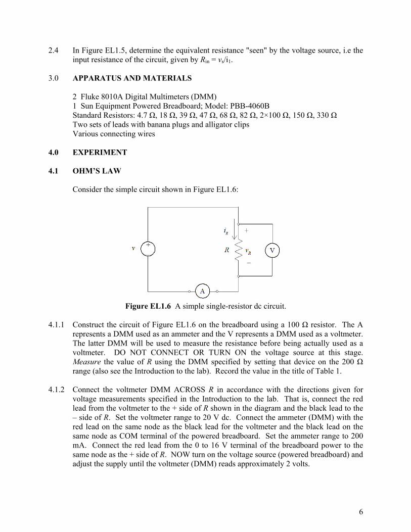
6
24 In Figure EL15 determine the equivalent resistance seen by the voltage source ie the input resistance of the circuit given by Rin = vsi1
30 APPARATUS AND MATERIALS
2 Fluke 8010A Digital Multimeters (DMM) 1 Sun Equipment Powered Breadboard Model PBB-4060B Standard Resistors 47 Ω 18 Ω 39 Ω 47 Ω 68 Ω 82 Ω 2times100 Ω 150 Ω 330 Ω Two sets of leads with banana plugs and alligator clips Various connecting wires
40 EXPERIMENT 41 OHMrsquoS LAW Consider the simple circuit shown in Figure EL16
Figure EL16 A simple single-resistor dc circuit
411 Construct the circuit of Figure EL16 on the breadboard using a 100 Ω resistor The A
represents a DMM used as an ammeter and the V represents a DMM used as a voltmeter The latter DMM will be used to measure the resistance before being actually used as a voltmeter DO NOT CONNECT OR TURN ON the voltage source at this stage Measure the value of R using the DMM specified by setting that device on the 200 Ω range (also see the Introduction to the lab) Record the value in the title of Table 1
412 Connect the voltmeter DMM ACROSS R in accordance with the directions given for
voltage measurements specified in the Introduction to the lab That is connect the red lead from the voltmeter to the + side of R shown in the diagram and the black lead to the ndash side of R Set the voltmeter range to 20 V dc Connect the ammeter (DMM) with the red lead on the same node as the black lead for the voltmeter and the black lead on the same node as COM terminal of the powered breadboard Set the ammeter range to 200 mA Connect the red lead from the 0 to 16 V terminal of the breadboard power to the same node as the + side of R NOW turn on the voltage source (powered breadboard) and adjust the supply until the voltmeter (DMM) reads approximately 2 volts
7
413 Record the voltmeter reading and the ammeter reading for the situation in 412 in Table 1 Adjust the power supply to give voltmeter readings of approximately 5 8 11 and 14 volts making sure to read the corresponding ammeter readings Record all voltmeter and corresponding ammeter readings in Table 1
414 From the data of Table 1 plot a graph of voltage versus current and from it determine the
value of R Compare this value with the value of R measured using the DMM in 411 and suggest possible reasons for any discrepancy
TABLE 1 - Voltage and Current Measurements for a _____Ω Resistor
Voltage (V) plusmn(01+1digit)
Current (A) plusmn(03+1digit)
These accuracies for the voltage and currents are found on the bottom of the 8010A 42 VOLTAGE AND CURRENT MEASUREMENTS FOR A SIMPLE SERIES CIRCUIT 421 On the breadboard set up the circuit of Figure EL17 but do not yet connect the voltage
source Resistor R1 is the standard 100 Ω used in part 41 Record its measured value in Table 2 Again using the DMM as an ohmmeter measure the standard 150 Ω resistor and also record its value in Table 2
422 Now connect the voltage source (using the red lead from the 0-16 V to node A and the
Figure EL17 A series circuit with two resistors Note the chosen polarities for the voltages and
the directions for the currents
8
black lead from the COM terminal to node B) Using one of the DMMs as a voltmeter set to read dc volts switch on the source and adjust it to give a reading of +10 V dc on the DMM 423 Measure the voltages across R1 and R2 with the polarities shown Record the readings in Table 2 424 Using the second DMM measure and record in Table 2 the currents through each
resistor taking into account the correct sign as indicated by the directions in Figure EL17
425 Using the measured quantities calculate the power dissipated by each resistor Record
the results in Table 2 426 Compare the measured and standard values of the resistances and the measured and
calculated values of the currents voltages and power Comment on the results 427 Verify that the power delivered by the voltage source is equal to the total power
dissipated by the resistors
TABLE 2 ndash Resistance Current and Voltage Measurements
ParameterVariable Calculated or Standard
(Prelab)
Measured
R1 (Ω)
R2 (Ω)
i1 (mA)
i2 (mA)
vAB (V) v1 (V) v2 (V) P1 (W) P2 (W)
sumPdev (W) sumPdiss (W)
9
43 POWER TRANSFER TO A LOAD RESISTOR Here we use the same circuit set-up as in Figure EL17 but now we will consider that R2
is a load resistor (RL) and we wish to determine the power absorbed by the load for various resistive values while keeping R1 fixed at its measured value found in step 421 Also notice that the polarities have been changed (this is an arbitrary decision) ndash see Figure EL18
Figure EL18 A series circuit containing a single resistor R1 connected to a resistive load RL
431 Using the DMM as an ohmmeter measure the following standard resistors and record the
values in Table 3 47 Ω 18 Ω 39 Ω 47 Ω 68 Ω 82 Ω 100 Ω 150 Ω 330 Ω The 100 Ω resistor is in addition to the one used in part 421 Also you have already measured the 150 Ω resistor and may use its value as found in 421
432 With RL (ie R2) taking the successive measured values of the 47 Ω 18 Ω 39 Ω 47 Ω
68 Ω 82 Ω 100 Ω 150 Ω and 330 Ω resistors use the DMM as a voltmeter to determine the load voltage vL across RL When the 47 Ω and 18 Ω resistors are used for RL it might be useful to set the DMM on the 2 V range For the other resistors use the 20 V range Record all voltage readings in Table 3 433 Using the measured values for vL and RL calculate and record in Table 3 the power absorbed by each load resistor 415 From the data of Table 3 plot a graph of Load Power versus Load Resistance sketch a
smooth curve through the points and from this graph observe and record the value of RL for which the maximum power is absorbed How does this resistance compare with R1 How does the power absorbed by R1 compare with that absorbed by the load resistor when the latter absorbs maximum power
50 CONCLUSIONS State a conclusion for each of the three parts of the experiment
10
TABLE 3 ndash Load Power Measurements
Standard Value of RL (Ω)
Measured Value of RL (Ω)
Load Voltage vL (V)
Load Power PL (W)
47 18 38 47 68 82 100 150 330
11
APPENDIX A (Taken from a Laboratory Manual for the former Engineering 1333 Basic Electrical
Concepts and Circuits course prepared by Dr J Quaicoe) Figure A1 shows the color code for carbon composition resistors along with the procedure for determining the resistance and tolerance from the color codes Table A1 gives a list of readily available standard values of resistors (The Boldface figures are available in the laboratory) If a designer requires other than a standard value such as 38 kΩ then a 39 kΩ resistor will probably be employed since a 38 kΩ resistor falls within the limits of a 39 kΩ resistor with a 10 tolerance
Figure A1 Color code for carbon composition [2] Example Find the resistance value and the tolerance of a resistor having the following color
bands
A - Gray B - Red
C - Black D - Silver
Solution Gray = 8 Red = 2 Black = 0
Silver = plusmn 10
From R = AB Η 10C tolerance = D
R = 82 Η 100 plusmn 10
= 820 Ω plusmn 82 Ω
12
Table A1 Standard Values of Resistors
Ohms (Ω)
Kilohms
(kΩ)
Megohms
(MΩ) 010 10 10 100 1000 011 11 11 110 1100 012 12 12 120 1200 013 13 13 130 1300 015 15 15 150 1500 016 16 16 160 1600 018 18 18 180 1800 020 20 20 200 2000 022 22 22 220 2200 024 24 24 240 2400 027 27 27 270 2700 030 30 30 300 3000 033 33 33 330 3300 036 36 36 360 3600 039 39 39 390 3900 043 43 43 430 4300 047 47 47 470 4700 051 51 51 510 5100 056 56 56 560 5600 062 62 62 620 6200 068 68 68 680 6800 075 75 75 750 7500 082 82 82 820 8200 091 91 91 910 9100
10 100 11 110 12 120 13 130 15 150 16 160 18 180 20 200 22 220 24 240 27 270 30 300 33 330 36 360 39 390 43 430 47 470 51 510 56 560 62 620 68 680 75 750 82 820 91 910
10 100 11 110 12 120 13 130 15 150 16 160 18 180 20 200 22 220 24 27 30 33 36 39 43 47 51 56 62 68 75 82 91
13
Sample Graph
Note the labeling in the following graph which is meant only as an example of how data should be presented graphically Specifically note (1) title (2) name symbol and unit for both the abscissa and ordinate (3) both axes labeled with appropriate scales (4) data points indicated (here small crosses are used) and a best-fit curve drawn through the data points which may or may not lie on the curve itself There are ways of calculating a curve of best-fit but here we simply ldquoguessrdquo how the curve may most accurately be drawn to represent the overall nature of the data In this example our guess is that the curve of best-fit is a straight line
000 003 006 009 012 015
Current i (A)
0
3
6
9
12
15
Vol
tage
v (V
)
Voltage vs Current for a Linear Resistor
14
EXP 1040-EL2 CIRCUIT LAWS AND TROUBLESHOOTING PURPOSE
To (i) further verify the validity of the basic circuit laws ie Ohms law and Kirchhoffs Laws when applied to a resistive circuit and (ii) briefly examine some simple ideas associated with troubleshooting a circuit 10 INTRODUCTION
Circuit analysis is the process by which all voltages and currents associated with each element in a given circuit are evaluated Conversely circuit synthesis (or circuit design) involves determining the necessary circuit element values and their interconnection in order to achieve desired voltages and currents Two simple but sufficient laws form the basis for electric circuit analysis and synthesis The first of these describes the characteristics or properties of a particular element irrespective of how it is connected to other elements in a circuit It is often expressed in terms of the current THROUGH and voltage ACROSS the element ie the i-v characteristics of the element and is named Ohms law The second is a network law that applies to the interconnection of elements rather than to individual elements The law describes the inherent constraints on voltage and current variables by virtue of interconnections and is expressed in Kirchhoffs laws which really follow from the conservation of energy and continuity of current (or conservation of charge) principle
In this experiment the basic laws are examined by investigating the behaviour of a simple circuit 11 Ohms Law
Ohms Law is based on a linear relationship between voltage and current Ohms Law states that the voltage across many types of conducting materials is directly proportional to the current flowing through the material It is expressed mathematically as v = Ri 11 where the constant of proportionality R is called the RESISTANCE A resistance for which the voltage versus current relationship is a straight line is a LINEAR RESISTANCE A linear resistance obeys Ohms Law because the resistance is always constant However a resistance whose ohmic value does not remain constant is defined as a NONLINEAR RESISTANCE Many resistors lose their linearity as the operating conditions (eg temperature) changes 12 The Electric Circuit
An electric circuit consists of circuit elements such as energy sources and resistors connected by electrical conductors or leads to form a closed path or combination of paths through which current can flow A point at which two or more elements have a common connection is called a NODE A two-terminal circuit element connected between two nodes is called a BRANCH A branch may contain more than one element between the same nodes
15
When two or more circuit elements are connected together an ELECTRIC NETWORK is formed If the network contains at least one closed path the network is called an ELECTRIC CIRCUIT 13 Kirchhoffs Laws 131 Kirchhoffs Current Law (KCL)
Kirchhoffs current law describes current relations at any node in a lumped network It states that the algebraic sum of the currents entering (or leaving) any node or cutset (supernode) is zero (The idea of a supernode is not part of this course) Kirchhoffs current law relates to the conservation of charge since a node cannot store destroy or generate charge It follows that the charge flowing out of a node exactly equals the charge flowing into the node An equivalent way of saying this is to say that the current at a node is continuous 132 Kirchhoffs Voltage Law (KVL)
Kirchhoffs voltage law describes voltage relations in any closed path in a lumped network It states that the algebraic sum of the voltages around any closed path is zero Kirchhoffs voltage law expresses the principle of conservation of energy in terms of the voltages around a closed path Thus the energy lost by a charge travelling around a closed path is equal to the energy gain 14 Voltage Notations
It is usual to express all potentials in a circuit with respect to a reference point (assumed to have zero potential) For example the potential of point A or the voltage of point A with respect to some reference point is indicated as vA The potential of a point with respect to a second point other than the reference point is indicated by a double subscript For example in Figure EL21 the potential of A with respect to B is indicated as vAB The second subscript indicates the reference point Thus the potential of B with respect to A is represented by vBA
Figure EL21 Voltage notation Note that vBA = ndash vAB REFERENCES [1] The Introduction and Appendix A of laboratory exercise EXP 1040-EL1 [2] EW Gill Engineering1040 Mechanisms and Electric Circuits Electric Circuits Module 2008 [3] S Wolf and R Smith Electronic Instrumentation Laboratories Prentice-Hall NJ 1990
16
20 PRELAB 21 Read Section 1 of EXP 1040-EL1 and pages 13ndash26 of Reference [2] 22 Determine the colour coding for each of the following resistors
i) 820 kΩ ii) 1 kΩ iii) 68 MΩ iv) 18 MΩ 23 Consider the circuit of Figure EL22
i) Write the Kirchhoffrsquos voltage law equations for loops adba and adcba ii) Write the Kirchhoffrsquos current law equations for nodes d and c iii) Use the four equations in (i) and (ii) to find the currents i1 i2 i3 and i4 iv) Find the voltages across the resistors having the polarities shown in the figure v) Determine the power dissipated by each resistor vi) Find the power supplied by the source and compare with the total power
developed in the circuit 24 In Figure EL22 determine the equivalent resistance seen by the voltage source ie the
input resistance of the circuit given by Rin = vABi1 25 Troubleshooting is the process of identifying and locating a failure (fault) or problem in a
circuit Generally the problems are due to open circuits or short circuits Consider the circuit of Figure EL22 A DMM set to measure the voltage across R4 reads vCB = 228 V Determine if there is a fault in the circuit If there is a fault identify it as either a short or open circuit
30 APPARATUS AND MATERIALS
1 Fluke 8010A Digital Multimeter (DMM) 1 Sun Equipment Powered Breadboard Model PBB-4060B Standard Resistors 2times100 Ω 150 Ω 220 Ω One set of leads with banana plugs and alligator clips Various connecting wires
40 EXPERIMENT 41 RESISTANCE MEASUREMENT USING THE DMM 411 With the DMM set to measure RESISTANCE measure and record in Table 1 the
resistance of each resistor in the circuit of Figure EL22 Note that the resistance of each resistor must be measured separately Also record the standard values
412 Construct the circuit of Figure EL22 on the breadboard provided Do not connect the
voltage source to the circuit With the DMM set to read RESISTANCE connect the DMM to nodes a and b and record the equivalent resistance of the resistive circuit as Rin in Table 1 Also record in Table 1 Rin calculated using the values measured in 411
17
vab = +8 V R1 = 100 Ω R2 = 220 Ω R3 = 150 Ω R4 = 100 Ω
Figure EL22 Series-parallel circuit for analysis and experimentation
42 VOLTAGE AND CURRENT MEASUREMENTS USING THE DMM 421 Connect the voltage source to the resistive circuit at points a (red lead) and b (black lead)
Set the DMM to read dc volts and adjust the 0 to 16 V voltage source from the breadboard to give a +8 V dc reading on the DMM Record this as vab in Table 1 Note It may not be possible to adjust the source to read exactly +8 V ndash simply record the closest value that you are able to obtain
422 Recall the voltage measurement technique from the information given in Lab 1 Measure and record in Table 1 the dc voltages across the resistors in the circuit of Figure EL22
with the polarities as specified Set the DMM on the most appropriate range for these measurements
423 Recall the current measurement technique from the information given in Lab 1 With the
DMM set on dc amps measure the current flowing in each resistor with the directions specified in Figure EL22 Record the results in the Table 1
424 Using the measured quantities calculate the power dissipated by each resistor Record
the results in Table 1 425 Compare the measured (or lsquostandardrsquo in case of the resistors) and calculated results of the
resistances currents voltages and power Comment on the results 426 From the results for the measured voltages in Table 1 verify that (within expected errors)
KVL has been satisfied for (i) mesh adba (ii) loop adcba and (iii) mesh dcbd Briefly discuss any discrepancy Note a mesh is a loop that does not contain any other loop(s) For example in this circuit loop adcba contains mesh adba and mesh dcbd
18
427 From the results for the measured currents in Table 1 verify that (within expected errors) KCL has been satisfied for (i) node d and (ii) node c Briefly discuss any discrepancy
428 Verify that the power delivered by the voltage source is equal to the total power
dissipated by the resistors 43 TROUBLESHOOTING 431 Verify the troubleshooting problem in Section 25 432 Provide an analysis of the problem and discuss the conceptual basis for identifying the
type of fault 50 CONCLUSIONS
19
TABLE 1 ndash Resistance Current and Voltage Measurements
ParameterVariable
Standard or Calculated
Measured
R1 (Ω)
R2 (Ω)
R3 (Ω)
R4 (Ω)
Rin (Ω)
vab (V)
v1 (V)
v2 (V)
v3 (V)
v4 (V)
i1 (mA)
i2 (mA)
i3 (mA)
i4 (mA)
P1 (W)
P2 (W)
P3 (W)
P4 (W)
Pdev (W)
Pdiss (W)
20
APPENDIX A (Modified from the former Engineering 1333 Lab manual by Dr John Quaicoe)
This appendix contains several important ideas that will be useful in any of your encounters with real electric circuits In reality measurements in a circuit will depend on all elements of the circuit and all connectors as well as on the operating conditions A1 Resistors
The flow of charge through any material encounters an opposing force This opposition due to the collisions between electrons and between electrons and other atoms in the material which converts electrical energy into heat is called the resistance of the material A device specifically designed to have resistance is called a resistor A11 Factors Which Affect Resistance
The resistance of any material with a uniform cross sectional area depends on the material used the length the cross-sectional area and temperature under which operation occurs Conductor Length and Cross Sectional Area
If the effects of temperature are neglected resistance depends directly on the length of the material and inversely on the cross-sectional area In equation form the resistance of a conductor at room temperature of 20oC is expressed as R = ρlA (A1) where R is the resistance in ohms
l is the length in metres or feet A is the cross-sectional area in m2 or circular mils (CM) ρ is the resistivity or specific resistance in Ωmiddotm or ΩmiddotCMft
Electrical conductors are generally circular in cross-section with wire diameters measured
in mils 1 mil = 11000 in = 10-3 in (A2) The cross-sectional area of a conductor is for convenience defined in circular mils The circular mil is the area of a circular cross-section having a diameter of 1 mil Area (circle) = πd24 (A3) Since the area depends on the square of the diameter for any arbitrary diameter d in mils the area in circular mils is given by A = d2 cir mils (CM) (A4)
It is still quite common to define the resistivity in the Imperial (English) system as the resistance of a 1 ft length of conductor with an area of 1 CM Of course the SI unit for
21
resistivity as is easily deduced from equation (A1) will be the Ωmiddotm Table A1 lists resistivity values of common conducting materials in both SI and Imperial units
Table A1 The resistivities of common conducting materials at 20oC
Conducting Material
Resistivity (Ωm)
Resistivity (Ωcir milft)
Aluminum
283 x 10-8
170
Brass
7 x 10⁻⁸
420
Copper annealed
172 x 10-8
1037
Copper hard-drawn
178 x 10-8
107
Gold
245 x 10-8
147
Lead
221 x 10-8
132
Nichrome
100 x 10-8
600
Platinum
10 x 10-8
602
Silver
164 x 10-8
99
Tin
115 x 10-8
692
Tungsten
552 x 10-8
332
Zinc
623 x 10-8
374
Examples 1 An annealed copper bar measures 1 x 3 cm and is 12 m long What is the resistance
between the ends of the bar
Solution R = ρlA = (172 x 10-8) x (5 x 10-1)(1 x 10-2 x 3 x 10-2)
= 285 x 10-5 Ω
2 Find the resistance of an annealed copper wire 200 ft long with a 100 mil diameter
Solution A(cir mil) = d2 = (100)2 = 104 CM R = ρlA = (1037) x (200)104 = 207 x 10ndash2 Ω
22
Temperature Effects
For most conductors as the temperature increases either from current flowing through it or by heat absorption from the surrounding medium the resistance increases This is due to the increased molecular movement within the conductor which hinders the flow of charge The resistance increases almost linearly with increase in temperature
The relationship between temperature and resistance is expressed as (|T| + t1)R1 = (|T| +t2)R2 (A5) where |T| is the inferred absolute zero of the material involved in oC R1 is the resistance of the material at the temperature t1
oC R2 is the resistance of the material at the temperature t2
oC
The relationship between temperature and resistance may be expressed by
R2 = R1 [1 + α1(t2 - t1)] (A6) where α1 is the temperature coefficient of resistance
R1 is the resistance at the temperature t1 and
R2 is the resistance at the temperature t2
Table A2 lists the inferred absolute zero and temperature coefficients of common conducting materials
Most materials exhibit an increase in resistance with an increase of temperature and are said to have a positive temperature coefficient of resistance However some materials such as carbon and semiconductor materials exhibit a decrease in resistance with an increase of temperature and are said to have a negative temperature coefficient of resistance Examples 1 What is the resistance of an annealed copper wire at 10oC if the resistance is 50 Ω at
60oC
Solution (|T| + t1)R1 = (|T| +t2)R2 t2 = 60o R2 = 50 Ω |T| = 2345o
t1 = 10oC R1 =
R1 = (|T| + t1) R2 (|T| + t2)
= 50 x (2445)(2945) = 415 Ω
23
2 What is the resistance of a copper wire at 10oC if the resistance at 20oC is 433 Ω and if
α1 = 000393
Solution
R2 = R1(1 + α1 ΔT)
= 433 [1 + 000393 (10-20)] = 416 Ω
Table A2 Inferred absolute zero and temperature coefficients for common conducting materials
Conducting
Material
Inferred Absolute zero (C)
Temperature coefficient (Ω CΩ at 0oC)
Aluminum
-236
000424
Brass
-480
000208
Copper annealed
-2345
000427
Copper hard drawn
-242
000413
Gold
-274
000365
Lead
-224
000466
Nichrome
-2270
000044
Platinum
-310
000323
Silver
-243
000412
Tin
-218
000458
Tungsten
-202
000495
Zinc
-250
000400
24
A1 2 Wire Tables [3] Circular cross-section wire is designed by a gauge size of number representing a certain diameter wire The wire table is designed primarily to standardize the size of wire produced by manufacturers The American Wire Gauge (AWG) sizes are given in Table A3 Note that the larger the gauge number the smaller the diameter of the conductor
Table A3 American Wire Gauge (AWG) Sizes of Copper Wire [3]
APPLICATIONS
AWG
AREA (CM)
Ω1000 ft (200 C)
Max Current
(900 C) Power distribution
00
133100
0078
186
1
83690
0124
137
4
41470
0240
89
House main power carriers
6
26240
0395
65
8
16510
0620
48
Lighting outlets general home use
12
6530
1588
20
14
4110
252
15
Television radio
20
10215
101
-
22
6424
161
-
Telephone instruments
28
1598
649
-
35
315
3290
-
40
99
10490
-
An examination of the table shows that if the gauge number changes by 10 the cross-
sectional area changes by approximately a factor of 10 Thus the resistance also changes by approximately 10 times For example AWG 4 has a cross-sectional area of 41470 CM and resistance of 0240 Ω1000 ft whereas AWG 14 has a cross-sectional area of 4110 CM and a resistance of 252 Ω1000 ft ie an increase of 10 in the gauge number represents a decrease in the area by a factor of approximately 10 and an increase in the resistance by a factor of approximately 10 A13 Types of Resistors
Resistors are used for many purposes and are therefore made in many forms The most common of the resistor types are the carbon composition resistor the wirewound resistor the
25
metal film resistor and the carbon film resistor They all belong in either of two groups fixed or variable
The most common of the low-wattage fixed-type resistors is the carbon composition resistor It is made of hot-pressed carbon granules mixed with varying amounts of binding material to achieve a large range of resistance values They are used extensively in electronic applications They are relatively inexpensive reliable and free of stray capacitance and inductance They are available in power ratings up to 2W with resistance values in the range of 1 to 22 MΩ and 5 to 20 tolerance The resistance value of carbon composition resistors and tolerances are specified by a set of colour-coded bands painted on the resistor body Each colour represents a digit in accordance with Figure A1 in the appendix of Exp 1040-EL1 The resistance value as indicated by the colour bands of carbon composition resistors is called the nominal value of resistance Wire wound resistors are commercially available for high precision low resistance and high power dissipation applications They usually consist of Nichrome or copper-nickel wire wound on a ceramic tube and protected from mechanical and environmental hazards by a protective coating of vitreous enamel or silicone Their resistance values range from 1Ω to 100 kΩ with a tolerance range of 00005 and above and a maximum power rating of 200 W
A third group of resistors consist of a thin film of material deposited on insulating materials to provide very high resistance paths Depending on the material used the resistors are classified as carbon film metal film or metal-oxide film resistors Their values range up to 10000 MΩ
Variable resistors come in many forms but basically they can be separated into the linear or non-linear types Variable resistors usually have three leads two fixed and one moveable If contacts are made to only two leads of the resistor the variable resistor is being employed as a rheostat If all three contacts are used in a circuit it is termed as potentiometer or pot The value of the overall resistance and the power ratings of variable resistors are usually stamped on their cases Because the resistance of a conducting film varies with length cross-section and temperature it is possible to use resistance measurement to sense changes in any of those parameters A device that responds to one physical effect is called a transducer Electrical transducers are often used in instrumentation for non-electrical quantities such as temperature light and strain The resistance of the device can be measured and the magnitude of the physical or chemical parameter inferred from the resistance value Typical examples of resistive transducers are 1 The thermistor a two-terminal semiconductor device designed specifically to exhibit a
change in electrical resistance with a change in its body temperature 2 The strain gauge a device which converts linear dimension changes into resistive
changes 3 The photoconductive cell a two-terminal device whose resistance depends upon the
intensity of light impinging on the cell
EXP 1040-EL3 Applications of Resistive Networks PURPOSE To (1) investigate the idea of voltage division using a single source and (2) to examine the utility of a Wheatstone bridge circuit for resistance measurements 10 INTRODUCTION
Using the laws discussed in the course material ndash namely Ohmrsquos law Kirchhoffrsquos Voltage Law (KVL) and Kirchhoffrsquos Current Law (KCL) ndash we are now in a position to study many different circuits having a variety of real-world applications In this lab we consider two such applications and while the analysis associated with them is relatively straight forward they are of significant modern-day importance 11 Voltage Divider Circuits
A voltage source is sometimes required to supply a particular voltage to a load and in fact it may be required to supply several loads with certain specified voltages simultaneously Ideally the voltage supplied should not depend on the size of the load
As a first example consider the circuit shown in Figure EL31 in which a simple voltage
divider circuit is connected in series with the load Notice the situation has been depicted in two equivalent ways In the second schematic the negative terminal of the source is assumed to be electrical ground An electrical ground is a reference level from which other voltages are measured An ideal electrical ground can absorb an unlimited amount of current without changing its potential Here then conventional current flows from the positive terminal of the source through the resistors and back to the source via the ground path (the closed path connection is not explicit in the schematic diagram but it is understood)
Figure EL31 Two equivalent schematics (a) and (b) for a simple voltage divider
From Section E251 of the class notes Electric Circuits Module we know that
⎥⎦
⎤⎢⎣
⎡+
=Ls
LsL RR
Rvv (1)
26
However this type of voltage divider has a serious disadvantage since the value of vL depends on the value of iL and the latter will change depending on the value of the load resistance
To help overcome the problem referred to above it is possible to construct a voltage divider with a bleeder resistor RB as shown below in Figure EL32 and as discussed in Section 251 (page 29) of the class notes Electric Circuits Module
Figure EL32 Two representations (a) and (b) of a voltage divider with a bleeder resistor Strictly the voltage across the parallel section of the circuit is (by the voltage divide lsquorulersquo)
⎥⎦
⎤⎢⎣
⎡+
=)||(
||
BS
LBsL
LRRRRRvv (2)
where
⎥⎦
⎤⎢⎣
⎡+
=LRR
RRRRB
LBLB || (3)
As shown in the class notes the advantage of this kind of voltage division is that when RBltltRL the load voltage is essentially independent of the load resistance and
⎥⎦
⎤⎢⎣
⎡+
=BS
BsL RR
Rvv (4)
Because the load voltage is less affected by the load resistance in this situation we say there is better voltage regulation in this circuit than that in Figure EL31 12 The Wheatstone Bridge The Wheatstone bridge circuit is mainly used to measure an unknown resistance However the principle of the Wheatstone bridge is used in many transducers ndash devices that convert one kind of energy into another ndash and instrumentation systems to measure a physical variable such as 27
strain temperature and pressure A Wheatstone bridge circuit is shown in Figure EL33 In this figure R3 is a variable resistance which models the transducer If a change in physical variable results in a change in resistance of the transducer the Wheatstone bridge can be used to convert the change in resistance to a change in voltage which can be measured
Figure EL33 A Wheatstone bridge
When the voltage vab is zero the bridge is said to be balanced If two resistances (say R1 and R2) are known and another (say Rx) is unknown then a fourth adjustable known resistance R3 (potentiometer) can be used to determine the unknown resistance Rx under balanced conditions When R3 is actually a transducer whose resistance changes with some change in a physical parameter such as temperature then if R1 R2 and Rx are known the voltage vab is an indicator of the size of the measured parameter Balanced Conditions As noted for balanced conditions the voltage vab is zero Also under these conditions using the voltage divide rule twice gives
⎥⎦
⎤⎢⎣
⎡+
=x1
x
RRRvvad (5)
⎥⎦
⎤⎢⎣
⎡+
=32
3
RRRvvbd (6)
We have also seen from Section 254 of the Electric Circuits Module lecture notes that
32
1x R
RRR ⎟⎟
⎠
⎞⎜⎜⎝
⎛= (7)
Unbalanced Conditions When the bridge is not balanced ndash ie vab ne 0 ndash then using Kirchhoffrsquos laws it is straight forward to show that
⎥⎦
⎤⎢⎣
⎡+
minus+
=32
3
x1
x
RRR
RRRvvab (8)
28
29
From this equation we see immediately that if any three of the resistances are fixed in value then a change in the other resistance results in a change in vab Thus a variation in vab is effectively a measure of a change in the variable resistance REFERENCES [1] The Introduction and Appendix A of laboratory exercise EXP 1040-EL1 [2] EW Gill Engineering1040 Mechanisms and Electric Circuits Electric Circuits Module 2008 20 PRELAB 21 Carefully read Section 1 (Introduction) of this experiment and the sections referred to in reference [2] 22 Refer to Figure EL31 The series dropping resistor has a value of 10 kΩ (a) Determine the value of the load resistor RL so that vL = 75 V if the source voltage is 10 V (b) If the load resistance is increased by 25 calculate the new vL 23 Refer to Figure EL32 (a) Design a voltage divider (ie find Rs and RB) for the load
resistance RL obtained in part (a) of Question 22 so that it can operate at vL = 75 V from a 10 V source Assume that the bleeder current iB is 75 mA (b) If the load resistance is increased by 25 calculate the new load voltage Compare this result with that obtained in Question 22 (b) Comment on the comparison
30 APPARATUS AND MATERIALS
1 Fluke 8010A Digital Multimeter (DMM) 1 Sun Equipment Powered Breadboard Model PBB-4060B Standard Resistors 1 kΩ 3 times 120 Ω others as calculated in design Potentiometers 200 Ω 5 k Ω One set of leads with banana plugs and alligator clips and various connecting wires
40 EXPERIMENT 41 Voltage Divider 411 Familiarize yourself with potentiometers ndash the lab attendants will help On the breadboard construct the voltage divider circuit as shown in Figure EL31 using a 1 kΩ resistor for Rs and a 5 k Ω potentiometer (variable resistor) as the load resistor RL Ensure that the source voltage is 10 V after connecting to the circuit Adjust the variable resistor to get an output (load) voltage of vL = 75 V Measure the value of RL for this condition Comment on any discrepancies between the measured and calculated value in Question (22) of the Prelab
30
412 Vary the potentiometer resistance from 680 Ω to 5 k Ω and obtain the load voltage vL in each case Tabulate your results and plot vL as a function of RL 413 Construct the voltage divider found in Figure EL32 and measure the load voltages to
verify your design of Question 23 of the Prelab Use the nearest available resistance values to those you calculated in the design Comment on your findings
42 Wheatstone Bridge 421 On the breadboard construct the Wheatstone bridge circuit of Figure EL33 using three
120 Ω (nominal) resistors for R1 R2 and Rx and a 200 Ω potentiometer (pot) for R3 Also measure and record the actual values of the 120 Ω resistors Ensure that the source voltage v is 10 V after it is connected to the circuit Use the DMM as a voltmeter in the branch between nodes a and b
422 Adjust the pot until the bridge is balanced Measure and record the value of R3 for this
condition Confirm your observation by calculating R3 from equation (7) and comment on any discrepancies
50 DISCUSSION 51 Comment on probable applications of a voltage divider circuit 52 Discuss any technical difficulties encountered during the lab
_____________________________________________________________________________ EXP 1040-DL1 Introduction to Logic Gates and Ladder Diagrams PURPOSE To (i) familiarize the student with the basic logic gates AND OR NOT and NAND (ii) implement basic logic gates using relay logic and (iii) learn how to represent logic circuits by means of ladder diagrams 10 INTRODUCTION Logic circuits may be implemented (constructed) in a variety of ways perhaps most commonly today via electronic components In this lab and the next however we consider the implementation of basic logic expressions using a simple circuit board in conjunction with a few pneumatic cylinders This allows us to explore basic logic circuits without having to resort to sophisticated solid state circuitry (transistors etc) 20 PRELAB There is no prelab for this session However students need to read Section D13 pages 10-18 of the Digital Logic Module before the lab session 30 APPARATUS AND MATERIALS 1 Logic Board Various banana plug connectors AC power (from main lab supply) 40 EXPERIMENT
41 Board Familiarization 411 Normally-open Switch To gain familiarity with the laboratory test panel implement the simple circuit shown in Figure DL11 PB1 refers to one of the two push buttons available on the panel This specific circuit utilizes a ldquonormally openrdquo contact When PB1 is pressed the green indicator light should illuminate
31
CGreenPB1
24V N
Figure DL11 Simple circuit employing push button and a green indicator light
412 Normally-closed Switch Repeat exercise 411 using the ldquonormally closedrdquo contact of PB1 See Figure DL12
CGreen
24V N
PB1
Figure DL12 Simple circuit employing a normally closed contact
42 AND Gate
Using the two push buttons PB1 and PB2 implement an AND operation In other words the green indicator light should only illuminate if and only if both buttons are pressed simultaneously In your lab report provide
bull the ladder diagram implementation (similar to Figure DL11 or DL12) bull the standard symbol for a two input AND gate bull The truth table Note that the truth table should include all four combinations
of the two inputs Assume that a high or logic ldquo1rdquo occurs when the button is pressed
bull Provide a practical application of this circuit (hint think safety)
32
43 OR Gate
Repeat part 42 above in its entirety however this time implement an OR operation using the two push buttons PB1 and PB2 In this case the green indicator should illuminate if at least one of the two buttons is pressed For the practical application consider convenience instead of safety
44 OR Gate
Repeat part 42 above for a ldquoNANDrdquo gate Note that this will require normally closed contacts It is not necessary to provide a practical application for this circuit
45 NOR Gate
Repeat part 42 above for a NOR gate Note that this will require normally closed contacts It is not necessary to provide a practical application for this circuit
46 Inequality Comparator Figure DL13 represents a circuit that is sometimes referred to as an inequality comparator Implement the circuit and experimentally determine the truth table Note that this circuit employs both the ldquonormally openedrdquo and ldquonormally closedrdquo contacts of both push buttons In the lab report provide both the common name for this circuit as well as the standard logic symbol Why is this circuit referred to as an ldquoinequality comparatorrdquo
CGreen
24V N
PB1 PB2
PB_2PB_1
Figure DL13 Circuit that implements an ldquoinequality comparatorrdquo
47 Inverter
An inverter or NOT gate can be implemented with a relay as shown in Figure DL14 When the push button is pressed the coil of relay 1 is energized This opens the normally closed contact of relay 1 which turns the Green indicator light off Implement the circuit and experimentally determine the operation In the lab report provide the standard logic symbol for a NOT gate
33
CR1
24V N
PB2
R_1C
Green
Figure DL14 Circuit that implements a NOT gate
48 Latch (Priority on Set)
A relay can also be used to ldquolatchrdquo the state of the output such that the indicator light is illuminated when the push button is pressed and stays illuminated even if the button is released A second push button must be used to reset the circuit back to its initial (ldquoOFFrdquo) state In Figure DL15 PB1 energizes relay 1 when it is pressed One of the sets of contacts on relay 1 is used to maintain the relay energized even if PB1 is released The normally closed contact of button PB2 de-energizes the relay when the button is pressed (ie resets the latch) Implement the circuit and experimentally determine the operation Be sure and verify what happens when both buttons are pressed simultaneously Note that you must use a different set of relay contacts to energize the green indicator light This particular latching configuration is referred to as priority on SET
CR1
24V N
PB1
PB2
CGreen
R_1
R__1
Figure DL15 Implementation of a ldquolatchrdquo circuit using a relay
34
49 Latch (Priority on Re-Set)
An alternative latch configuration is implemented in Figure DL16 This configuration is referred to as priority on RESET Implement the circuit and experimentally determine the operation Be sure and verify what happens when both buttons are pressed simultaneously In terms of operation what is the main difference between ldquopriority on SETrdquo and ldquopriority on RESETrdquo Provide a practical application of both latch configurations (once again think safety)
CR1
24V N
PB1 PB2
CGreen
R_1
R__1
Figure DL16 Implementation of ldquopriority on RESETrdquo
35
_____________________________________________________________________________ EXP 1040-DL1 Introduction to Sequential Circuits Ladder Diagrams and Relay Logic PURPOSE To (i) introduce ladder diagrams and relay logic and (ii) demonstrate a simple pneumatic system 10 INTRODUCTION Ladder Diagrams (Figure DL21) are a graphical representation of sequential control circuits that are widely used in industry Although originally intended as a way of representing relay logic ladder diagrams are now the standard means of programming microprocessor based PLCs (Programmable Logic Controllers) They are prevalent in a many engineering fields including automation process control and manufacturing In this lab a sequential logic circuit will be implemented using the pneumatic test board The pneumatic test board has three pneumatic cylinders that are activated by solenoid valves The position of each cylinder is monitored by two limit switches One limit switch is activated when the cylinder is fully extended and the other is activated when the cylinder is fully retracted By energizing a solenoid you are able to extend a cylinder and by de-energizing the solenoid the cylinder will retract 20 PRELAB There is no prelab for this session However students need to read Unit D2 of the Digital Logic Module before the lab session 30 APPARATUS AND MATERIALS 1 Logic Board Various banana plug connectors AC power (from main lab supply) Compressed air source 40 EXPERIMENT
41 Limit Switch Familiarization
36
Limit switches A0 and A1 in Figure DL21 are used to sense when cylinder A is retracted and extended respectively Each switch incorporates both a normally opened and normally closed set of contacts Cylinders B and C employ switched B0 B1 and C0C1 respectively These six switches are identified on the wiring panel as S1 through S6 An indicator light can be used to verify the operation of the switches Sketch a circuit that illuminates the green light when cylinder A extends and the red light when cylinder A retracts Implement the circuit on the pneumatic test board and verify the operation by manually depressing the limit switches Use the circuit to determine the correspondence between the six limit switches and the wiring terminals S1 through S6
Figure DL21 Ladder diagram (left) for controlling two pneumatic cylinders 42 Solenoid Valve Familiarization
Solenoid valves S1 S2 and S3 control the three cylinders A B and C As shown in Figure DL21 when the solenoid valves are not energized the cylinders are retracted ie pressure is applied to the rod side of the cylinder Energizing the solenoid changes the position of the valve such that the cap side of the cylinder is pressurized and the
37
38
cylinder extends Sketch a circuit that extends cylinder A when push button PB1 is depressed and retracts A when the button is released Implement the circuit on the pneumatic test board and verify the operation There are a many ldquopinchrdquo points on the test board so be sure and keep your fingers away from the cylinders
43 Implementation of a Simple Latch
Using relay 1 design a circuit that latches the state of push button PB1 such that cylinder A extends when PB1 is depressed and stays extended even if PB1 is released The cylinder retracts only when push button PB2 is depressed Implement the circuit on the pneumatic test board and verify the operation
44 Sequential Logic Circuit 1 441 Familiarization with the Logic Sequence
The ladder diagram shown in Figure DL21 is a sequential logic circuit that will make two cylinders follow the sequence Cylinder A ndash extend -gt Cylinder B ndash extend -gt Cylinder A ndash retract -gt Cylinder B ndash retract The operation of the logic circuit can be described as follows
bull Push button PB1 initiates the start of the sequence ie extend cylinder A by activating solenoid A Relay 2 is latched when PB1 is depressed if and only if the last step in the sequence (limit switch B0 retract B) has been completed This also maintains solenoid A energized bull Once cylinder A has finished extending (ie switch A1 is active) the circuit advances to the second ldquorungrdquo of the ladder which activates solenoid B (cylinder B extends) bull When switch B1 is activated (ie B extended) the circuit advances to the third rung in the ladder Relay 4 is latched which in turn resets relay 2 de-energizing Solenoid A and retracting A bull In a similar fashion the fourth rung in the ladder resets relay 3 which retracts B bull Notice that each rung in the ladder is latched by the completion of the action associated with the previous rung
442 Implementation of the Logic Sequence
Implement the circuit described in 441 and verify the operation
45 Sequential Logic Circuit 2
Modify the circuit in section 44 to implement the following sequence
39
Cylinder A ndash extend -gt Cylinder B ndash extend -gt Cylinder B ndash retract -gt Cylinder A ndash retract
5 Lab Report 51 Provide a short written lab report that includes ladder diagrams of all the circuits design during the lab
52 Explain the operation of the circuit developed in part 45 above

8
black lead from the COM terminal to node B) Using one of the DMMs as a voltmeter set to read dc volts switch on the source and adjust it to give a reading of +10 V dc on the DMM 423 Measure the voltages across R1 and R2 with the polarities shown Record the readings in Table 2 424 Using the second DMM measure and record in Table 2 the currents through each
resistor taking into account the correct sign as indicated by the directions in Figure EL17
425 Using the measured quantities calculate the power dissipated by each resistor Record
the results in Table 2 426 Compare the measured and standard values of the resistances and the measured and
calculated values of the currents voltages and power Comment on the results 427 Verify that the power delivered by the voltage source is equal to the total power
dissipated by the resistors
TABLE 2 ndash Resistance Current and Voltage Measurements
ParameterVariable Calculated or Standard
(Prelab)
Measured
R1 (Ω)
R2 (Ω)
i1 (mA)
i2 (mA)
vAB (V) v1 (V) v2 (V) P1 (W) P2 (W)
sumPdev (W) sumPdiss (W)
9
43 POWER TRANSFER TO A LOAD RESISTOR Here we use the same circuit set-up as in Figure EL17 but now we will consider that R2
is a load resistor (RL) and we wish to determine the power absorbed by the load for various resistive values while keeping R1 fixed at its measured value found in step 421 Also notice that the polarities have been changed (this is an arbitrary decision) ndash see Figure EL18
Figure EL18 A series circuit containing a single resistor R1 connected to a resistive load RL
431 Using the DMM as an ohmmeter measure the following standard resistors and record the
values in Table 3 47 Ω 18 Ω 39 Ω 47 Ω 68 Ω 82 Ω 100 Ω 150 Ω 330 Ω The 100 Ω resistor is in addition to the one used in part 421 Also you have already measured the 150 Ω resistor and may use its value as found in 421
432 With RL (ie R2) taking the successive measured values of the 47 Ω 18 Ω 39 Ω 47 Ω
68 Ω 82 Ω 100 Ω 150 Ω and 330 Ω resistors use the DMM as a voltmeter to determine the load voltage vL across RL When the 47 Ω and 18 Ω resistors are used for RL it might be useful to set the DMM on the 2 V range For the other resistors use the 20 V range Record all voltage readings in Table 3 433 Using the measured values for vL and RL calculate and record in Table 3 the power absorbed by each load resistor 415 From the data of Table 3 plot a graph of Load Power versus Load Resistance sketch a
smooth curve through the points and from this graph observe and record the value of RL for which the maximum power is absorbed How does this resistance compare with R1 How does the power absorbed by R1 compare with that absorbed by the load resistor when the latter absorbs maximum power
50 CONCLUSIONS State a conclusion for each of the three parts of the experiment
10
TABLE 3 ndash Load Power Measurements
Standard Value of RL (Ω)
Measured Value of RL (Ω)
Load Voltage vL (V)
Load Power PL (W)
47 18 38 47 68 82 100 150 330
11
APPENDIX A (Taken from a Laboratory Manual for the former Engineering 1333 Basic Electrical
Concepts and Circuits course prepared by Dr J Quaicoe) Figure A1 shows the color code for carbon composition resistors along with the procedure for determining the resistance and tolerance from the color codes Table A1 gives a list of readily available standard values of resistors (The Boldface figures are available in the laboratory) If a designer requires other than a standard value such as 38 kΩ then a 39 kΩ resistor will probably be employed since a 38 kΩ resistor falls within the limits of a 39 kΩ resistor with a 10 tolerance
Figure A1 Color code for carbon composition [2] Example Find the resistance value and the tolerance of a resistor having the following color
bands
A - Gray B - Red
C - Black D - Silver
Solution Gray = 8 Red = 2 Black = 0
Silver = plusmn 10
From R = AB Η 10C tolerance = D
R = 82 Η 100 plusmn 10
= 820 Ω plusmn 82 Ω
12
Table A1 Standard Values of Resistors
Ohms (Ω)
Kilohms
(kΩ)
Megohms
(MΩ) 010 10 10 100 1000 011 11 11 110 1100 012 12 12 120 1200 013 13 13 130 1300 015 15 15 150 1500 016 16 16 160 1600 018 18 18 180 1800 020 20 20 200 2000 022 22 22 220 2200 024 24 24 240 2400 027 27 27 270 2700 030 30 30 300 3000 033 33 33 330 3300 036 36 36 360 3600 039 39 39 390 3900 043 43 43 430 4300 047 47 47 470 4700 051 51 51 510 5100 056 56 56 560 5600 062 62 62 620 6200 068 68 68 680 6800 075 75 75 750 7500 082 82 82 820 8200 091 91 91 910 9100
10 100 11 110 12 120 13 130 15 150 16 160 18 180 20 200 22 220 24 240 27 270 30 300 33 330 36 360 39 390 43 430 47 470 51 510 56 560 62 620 68 680 75 750 82 820 91 910
10 100 11 110 12 120 13 130 15 150 16 160 18 180 20 200 22 220 24 27 30 33 36 39 43 47 51 56 62 68 75 82 91
13
Sample Graph
Note the labeling in the following graph which is meant only as an example of how data should be presented graphically Specifically note (1) title (2) name symbol and unit for both the abscissa and ordinate (3) both axes labeled with appropriate scales (4) data points indicated (here small crosses are used) and a best-fit curve drawn through the data points which may or may not lie on the curve itself There are ways of calculating a curve of best-fit but here we simply ldquoguessrdquo how the curve may most accurately be drawn to represent the overall nature of the data In this example our guess is that the curve of best-fit is a straight line
000 003 006 009 012 015
Current i (A)
0
3
6
9
12
15
Vol
tage
v (V
)
Voltage vs Current for a Linear Resistor
14
EXP 1040-EL2 CIRCUIT LAWS AND TROUBLESHOOTING PURPOSE
To (i) further verify the validity of the basic circuit laws ie Ohms law and Kirchhoffs Laws when applied to a resistive circuit and (ii) briefly examine some simple ideas associated with troubleshooting a circuit 10 INTRODUCTION
Circuit analysis is the process by which all voltages and currents associated with each element in a given circuit are evaluated Conversely circuit synthesis (or circuit design) involves determining the necessary circuit element values and their interconnection in order to achieve desired voltages and currents Two simple but sufficient laws form the basis for electric circuit analysis and synthesis The first of these describes the characteristics or properties of a particular element irrespective of how it is connected to other elements in a circuit It is often expressed in terms of the current THROUGH and voltage ACROSS the element ie the i-v characteristics of the element and is named Ohms law The second is a network law that applies to the interconnection of elements rather than to individual elements The law describes the inherent constraints on voltage and current variables by virtue of interconnections and is expressed in Kirchhoffs laws which really follow from the conservation of energy and continuity of current (or conservation of charge) principle
In this experiment the basic laws are examined by investigating the behaviour of a simple circuit 11 Ohms Law
Ohms Law is based on a linear relationship between voltage and current Ohms Law states that the voltage across many types of conducting materials is directly proportional to the current flowing through the material It is expressed mathematically as v = Ri 11 where the constant of proportionality R is called the RESISTANCE A resistance for which the voltage versus current relationship is a straight line is a LINEAR RESISTANCE A linear resistance obeys Ohms Law because the resistance is always constant However a resistance whose ohmic value does not remain constant is defined as a NONLINEAR RESISTANCE Many resistors lose their linearity as the operating conditions (eg temperature) changes 12 The Electric Circuit
An electric circuit consists of circuit elements such as energy sources and resistors connected by electrical conductors or leads to form a closed path or combination of paths through which current can flow A point at which two or more elements have a common connection is called a NODE A two-terminal circuit element connected between two nodes is called a BRANCH A branch may contain more than one element between the same nodes
15
When two or more circuit elements are connected together an ELECTRIC NETWORK is formed If the network contains at least one closed path the network is called an ELECTRIC CIRCUIT 13 Kirchhoffs Laws 131 Kirchhoffs Current Law (KCL)
Kirchhoffs current law describes current relations at any node in a lumped network It states that the algebraic sum of the currents entering (or leaving) any node or cutset (supernode) is zero (The idea of a supernode is not part of this course) Kirchhoffs current law relates to the conservation of charge since a node cannot store destroy or generate charge It follows that the charge flowing out of a node exactly equals the charge flowing into the node An equivalent way of saying this is to say that the current at a node is continuous 132 Kirchhoffs Voltage Law (KVL)
Kirchhoffs voltage law describes voltage relations in any closed path in a lumped network It states that the algebraic sum of the voltages around any closed path is zero Kirchhoffs voltage law expresses the principle of conservation of energy in terms of the voltages around a closed path Thus the energy lost by a charge travelling around a closed path is equal to the energy gain 14 Voltage Notations
It is usual to express all potentials in a circuit with respect to a reference point (assumed to have zero potential) For example the potential of point A or the voltage of point A with respect to some reference point is indicated as vA The potential of a point with respect to a second point other than the reference point is indicated by a double subscript For example in Figure EL21 the potential of A with respect to B is indicated as vAB The second subscript indicates the reference point Thus the potential of B with respect to A is represented by vBA
Figure EL21 Voltage notation Note that vBA = ndash vAB REFERENCES [1] The Introduction and Appendix A of laboratory exercise EXP 1040-EL1 [2] EW Gill Engineering1040 Mechanisms and Electric Circuits Electric Circuits Module 2008 [3] S Wolf and R Smith Electronic Instrumentation Laboratories Prentice-Hall NJ 1990
16
20 PRELAB 21 Read Section 1 of EXP 1040-EL1 and pages 13ndash26 of Reference [2] 22 Determine the colour coding for each of the following resistors
i) 820 kΩ ii) 1 kΩ iii) 68 MΩ iv) 18 MΩ 23 Consider the circuit of Figure EL22
i) Write the Kirchhoffrsquos voltage law equations for loops adba and adcba ii) Write the Kirchhoffrsquos current law equations for nodes d and c iii) Use the four equations in (i) and (ii) to find the currents i1 i2 i3 and i4 iv) Find the voltages across the resistors having the polarities shown in the figure v) Determine the power dissipated by each resistor vi) Find the power supplied by the source and compare with the total power
developed in the circuit 24 In Figure EL22 determine the equivalent resistance seen by the voltage source ie the
input resistance of the circuit given by Rin = vABi1 25 Troubleshooting is the process of identifying and locating a failure (fault) or problem in a
circuit Generally the problems are due to open circuits or short circuits Consider the circuit of Figure EL22 A DMM set to measure the voltage across R4 reads vCB = 228 V Determine if there is a fault in the circuit If there is a fault identify it as either a short or open circuit
30 APPARATUS AND MATERIALS
1 Fluke 8010A Digital Multimeter (DMM) 1 Sun Equipment Powered Breadboard Model PBB-4060B Standard Resistors 2times100 Ω 150 Ω 220 Ω One set of leads with banana plugs and alligator clips Various connecting wires
40 EXPERIMENT 41 RESISTANCE MEASUREMENT USING THE DMM 411 With the DMM set to measure RESISTANCE measure and record in Table 1 the
resistance of each resistor in the circuit of Figure EL22 Note that the resistance of each resistor must be measured separately Also record the standard values
412 Construct the circuit of Figure EL22 on the breadboard provided Do not connect the
voltage source to the circuit With the DMM set to read RESISTANCE connect the DMM to nodes a and b and record the equivalent resistance of the resistive circuit as Rin in Table 1 Also record in Table 1 Rin calculated using the values measured in 411
17
vab = +8 V R1 = 100 Ω R2 = 220 Ω R3 = 150 Ω R4 = 100 Ω
Figure EL22 Series-parallel circuit for analysis and experimentation
42 VOLTAGE AND CURRENT MEASUREMENTS USING THE DMM 421 Connect the voltage source to the resistive circuit at points a (red lead) and b (black lead)
Set the DMM to read dc volts and adjust the 0 to 16 V voltage source from the breadboard to give a +8 V dc reading on the DMM Record this as vab in Table 1 Note It may not be possible to adjust the source to read exactly +8 V ndash simply record the closest value that you are able to obtain
422 Recall the voltage measurement technique from the information given in Lab 1 Measure and record in Table 1 the dc voltages across the resistors in the circuit of Figure EL22
with the polarities as specified Set the DMM on the most appropriate range for these measurements
423 Recall the current measurement technique from the information given in Lab 1 With the
DMM set on dc amps measure the current flowing in each resistor with the directions specified in Figure EL22 Record the results in the Table 1
424 Using the measured quantities calculate the power dissipated by each resistor Record
the results in Table 1 425 Compare the measured (or lsquostandardrsquo in case of the resistors) and calculated results of the
resistances currents voltages and power Comment on the results 426 From the results for the measured voltages in Table 1 verify that (within expected errors)
KVL has been satisfied for (i) mesh adba (ii) loop adcba and (iii) mesh dcbd Briefly discuss any discrepancy Note a mesh is a loop that does not contain any other loop(s) For example in this circuit loop adcba contains mesh adba and mesh dcbd
18
427 From the results for the measured currents in Table 1 verify that (within expected errors) KCL has been satisfied for (i) node d and (ii) node c Briefly discuss any discrepancy
428 Verify that the power delivered by the voltage source is equal to the total power
dissipated by the resistors 43 TROUBLESHOOTING 431 Verify the troubleshooting problem in Section 25 432 Provide an analysis of the problem and discuss the conceptual basis for identifying the
type of fault 50 CONCLUSIONS
19
TABLE 1 ndash Resistance Current and Voltage Measurements
ParameterVariable
Standard or Calculated
Measured
R1 (Ω)
R2 (Ω)
R3 (Ω)
R4 (Ω)
Rin (Ω)
vab (V)
v1 (V)
v2 (V)
v3 (V)
v4 (V)
i1 (mA)
i2 (mA)
i3 (mA)
i4 (mA)
P1 (W)
P2 (W)
P3 (W)
P4 (W)
Pdev (W)
Pdiss (W)
20
APPENDIX A (Modified from the former Engineering 1333 Lab manual by Dr John Quaicoe)
This appendix contains several important ideas that will be useful in any of your encounters with real electric circuits In reality measurements in a circuit will depend on all elements of the circuit and all connectors as well as on the operating conditions A1 Resistors
The flow of charge through any material encounters an opposing force This opposition due to the collisions between electrons and between electrons and other atoms in the material which converts electrical energy into heat is called the resistance of the material A device specifically designed to have resistance is called a resistor A11 Factors Which Affect Resistance
The resistance of any material with a uniform cross sectional area depends on the material used the length the cross-sectional area and temperature under which operation occurs Conductor Length and Cross Sectional Area
If the effects of temperature are neglected resistance depends directly on the length of the material and inversely on the cross-sectional area In equation form the resistance of a conductor at room temperature of 20oC is expressed as R = ρlA (A1) where R is the resistance in ohms
l is the length in metres or feet A is the cross-sectional area in m2 or circular mils (CM) ρ is the resistivity or specific resistance in Ωmiddotm or ΩmiddotCMft
Electrical conductors are generally circular in cross-section with wire diameters measured
in mils 1 mil = 11000 in = 10-3 in (A2) The cross-sectional area of a conductor is for convenience defined in circular mils The circular mil is the area of a circular cross-section having a diameter of 1 mil Area (circle) = πd24 (A3) Since the area depends on the square of the diameter for any arbitrary diameter d in mils the area in circular mils is given by A = d2 cir mils (CM) (A4)
It is still quite common to define the resistivity in the Imperial (English) system as the resistance of a 1 ft length of conductor with an area of 1 CM Of course the SI unit for
21
resistivity as is easily deduced from equation (A1) will be the Ωmiddotm Table A1 lists resistivity values of common conducting materials in both SI and Imperial units
Table A1 The resistivities of common conducting materials at 20oC
Conducting Material
Resistivity (Ωm)
Resistivity (Ωcir milft)
Aluminum
283 x 10-8
170
Brass
7 x 10⁻⁸
420
Copper annealed
172 x 10-8
1037
Copper hard-drawn
178 x 10-8
107
Gold
245 x 10-8
147
Lead
221 x 10-8
132
Nichrome
100 x 10-8
600
Platinum
10 x 10-8
602
Silver
164 x 10-8
99
Tin
115 x 10-8
692
Tungsten
552 x 10-8
332
Zinc
623 x 10-8
374
Examples 1 An annealed copper bar measures 1 x 3 cm and is 12 m long What is the resistance
between the ends of the bar
Solution R = ρlA = (172 x 10-8) x (5 x 10-1)(1 x 10-2 x 3 x 10-2)
= 285 x 10-5 Ω
2 Find the resistance of an annealed copper wire 200 ft long with a 100 mil diameter
Solution A(cir mil) = d2 = (100)2 = 104 CM R = ρlA = (1037) x (200)104 = 207 x 10ndash2 Ω
22
Temperature Effects
For most conductors as the temperature increases either from current flowing through it or by heat absorption from the surrounding medium the resistance increases This is due to the increased molecular movement within the conductor which hinders the flow of charge The resistance increases almost linearly with increase in temperature
The relationship between temperature and resistance is expressed as (|T| + t1)R1 = (|T| +t2)R2 (A5) where |T| is the inferred absolute zero of the material involved in oC R1 is the resistance of the material at the temperature t1
oC R2 is the resistance of the material at the temperature t2
oC
The relationship between temperature and resistance may be expressed by
R2 = R1 [1 + α1(t2 - t1)] (A6) where α1 is the temperature coefficient of resistance
R1 is the resistance at the temperature t1 and
R2 is the resistance at the temperature t2
Table A2 lists the inferred absolute zero and temperature coefficients of common conducting materials
Most materials exhibit an increase in resistance with an increase of temperature and are said to have a positive temperature coefficient of resistance However some materials such as carbon and semiconductor materials exhibit a decrease in resistance with an increase of temperature and are said to have a negative temperature coefficient of resistance Examples 1 What is the resistance of an annealed copper wire at 10oC if the resistance is 50 Ω at
60oC
Solution (|T| + t1)R1 = (|T| +t2)R2 t2 = 60o R2 = 50 Ω |T| = 2345o
t1 = 10oC R1 =
R1 = (|T| + t1) R2 (|T| + t2)
= 50 x (2445)(2945) = 415 Ω
23
2 What is the resistance of a copper wire at 10oC if the resistance at 20oC is 433 Ω and if
α1 = 000393
Solution
R2 = R1(1 + α1 ΔT)
= 433 [1 + 000393 (10-20)] = 416 Ω
Table A2 Inferred absolute zero and temperature coefficients for common conducting materials
Conducting
Material
Inferred Absolute zero (C)
Temperature coefficient (Ω CΩ at 0oC)
Aluminum
-236
000424
Brass
-480
000208
Copper annealed
-2345
000427
Copper hard drawn
-242
000413
Gold
-274
000365
Lead
-224
000466
Nichrome
-2270
000044
Platinum
-310
000323
Silver
-243
000412
Tin
-218
000458
Tungsten
-202
000495
Zinc
-250
000400
24
A1 2 Wire Tables [3] Circular cross-section wire is designed by a gauge size of number representing a certain diameter wire The wire table is designed primarily to standardize the size of wire produced by manufacturers The American Wire Gauge (AWG) sizes are given in Table A3 Note that the larger the gauge number the smaller the diameter of the conductor
Table A3 American Wire Gauge (AWG) Sizes of Copper Wire [3]
APPLICATIONS
AWG
AREA (CM)
Ω1000 ft (200 C)
Max Current
(900 C) Power distribution
00
133100
0078
186
1
83690
0124
137
4
41470
0240
89
House main power carriers
6
26240
0395
65
8
16510
0620
48
Lighting outlets general home use
12
6530
1588
20
14
4110
252
15
Television radio
20
10215
101
-
22
6424
161
-
Telephone instruments
28
1598
649
-
35
315
3290
-
40
99
10490
-
An examination of the table shows that if the gauge number changes by 10 the cross-
sectional area changes by approximately a factor of 10 Thus the resistance also changes by approximately 10 times For example AWG 4 has a cross-sectional area of 41470 CM and resistance of 0240 Ω1000 ft whereas AWG 14 has a cross-sectional area of 4110 CM and a resistance of 252 Ω1000 ft ie an increase of 10 in the gauge number represents a decrease in the area by a factor of approximately 10 and an increase in the resistance by a factor of approximately 10 A13 Types of Resistors
Resistors are used for many purposes and are therefore made in many forms The most common of the resistor types are the carbon composition resistor the wirewound resistor the
25
metal film resistor and the carbon film resistor They all belong in either of two groups fixed or variable
The most common of the low-wattage fixed-type resistors is the carbon composition resistor It is made of hot-pressed carbon granules mixed with varying amounts of binding material to achieve a large range of resistance values They are used extensively in electronic applications They are relatively inexpensive reliable and free of stray capacitance and inductance They are available in power ratings up to 2W with resistance values in the range of 1 to 22 MΩ and 5 to 20 tolerance The resistance value of carbon composition resistors and tolerances are specified by a set of colour-coded bands painted on the resistor body Each colour represents a digit in accordance with Figure A1 in the appendix of Exp 1040-EL1 The resistance value as indicated by the colour bands of carbon composition resistors is called the nominal value of resistance Wire wound resistors are commercially available for high precision low resistance and high power dissipation applications They usually consist of Nichrome or copper-nickel wire wound on a ceramic tube and protected from mechanical and environmental hazards by a protective coating of vitreous enamel or silicone Their resistance values range from 1Ω to 100 kΩ with a tolerance range of 00005 and above and a maximum power rating of 200 W
A third group of resistors consist of a thin film of material deposited on insulating materials to provide very high resistance paths Depending on the material used the resistors are classified as carbon film metal film or metal-oxide film resistors Their values range up to 10000 MΩ
Variable resistors come in many forms but basically they can be separated into the linear or non-linear types Variable resistors usually have three leads two fixed and one moveable If contacts are made to only two leads of the resistor the variable resistor is being employed as a rheostat If all three contacts are used in a circuit it is termed as potentiometer or pot The value of the overall resistance and the power ratings of variable resistors are usually stamped on their cases Because the resistance of a conducting film varies with length cross-section and temperature it is possible to use resistance measurement to sense changes in any of those parameters A device that responds to one physical effect is called a transducer Electrical transducers are often used in instrumentation for non-electrical quantities such as temperature light and strain The resistance of the device can be measured and the magnitude of the physical or chemical parameter inferred from the resistance value Typical examples of resistive transducers are 1 The thermistor a two-terminal semiconductor device designed specifically to exhibit a
change in electrical resistance with a change in its body temperature 2 The strain gauge a device which converts linear dimension changes into resistive
changes 3 The photoconductive cell a two-terminal device whose resistance depends upon the
intensity of light impinging on the cell
EXP 1040-EL3 Applications of Resistive Networks PURPOSE To (1) investigate the idea of voltage division using a single source and (2) to examine the utility of a Wheatstone bridge circuit for resistance measurements 10 INTRODUCTION
Using the laws discussed in the course material ndash namely Ohmrsquos law Kirchhoffrsquos Voltage Law (KVL) and Kirchhoffrsquos Current Law (KCL) ndash we are now in a position to study many different circuits having a variety of real-world applications In this lab we consider two such applications and while the analysis associated with them is relatively straight forward they are of significant modern-day importance 11 Voltage Divider Circuits
A voltage source is sometimes required to supply a particular voltage to a load and in fact it may be required to supply several loads with certain specified voltages simultaneously Ideally the voltage supplied should not depend on the size of the load
As a first example consider the circuit shown in Figure EL31 in which a simple voltage
divider circuit is connected in series with the load Notice the situation has been depicted in two equivalent ways In the second schematic the negative terminal of the source is assumed to be electrical ground An electrical ground is a reference level from which other voltages are measured An ideal electrical ground can absorb an unlimited amount of current without changing its potential Here then conventional current flows from the positive terminal of the source through the resistors and back to the source via the ground path (the closed path connection is not explicit in the schematic diagram but it is understood)
Figure EL31 Two equivalent schematics (a) and (b) for a simple voltage divider
From Section E251 of the class notes Electric Circuits Module we know that
⎥⎦
⎤⎢⎣
⎡+
=Ls
LsL RR
Rvv (1)
26
However this type of voltage divider has a serious disadvantage since the value of vL depends on the value of iL and the latter will change depending on the value of the load resistance
To help overcome the problem referred to above it is possible to construct a voltage divider with a bleeder resistor RB as shown below in Figure EL32 and as discussed in Section 251 (page 29) of the class notes Electric Circuits Module
Figure EL32 Two representations (a) and (b) of a voltage divider with a bleeder resistor Strictly the voltage across the parallel section of the circuit is (by the voltage divide lsquorulersquo)
⎥⎦
⎤⎢⎣
⎡+
=)||(
||
BS
LBsL
LRRRRRvv (2)
where
⎥⎦
⎤⎢⎣
⎡+
=LRR
RRRRB
LBLB || (3)
As shown in the class notes the advantage of this kind of voltage division is that when RBltltRL the load voltage is essentially independent of the load resistance and
⎥⎦
⎤⎢⎣
⎡+
=BS
BsL RR
Rvv (4)
Because the load voltage is less affected by the load resistance in this situation we say there is better voltage regulation in this circuit than that in Figure EL31 12 The Wheatstone Bridge The Wheatstone bridge circuit is mainly used to measure an unknown resistance However the principle of the Wheatstone bridge is used in many transducers ndash devices that convert one kind of energy into another ndash and instrumentation systems to measure a physical variable such as 27
strain temperature and pressure A Wheatstone bridge circuit is shown in Figure EL33 In this figure R3 is a variable resistance which models the transducer If a change in physical variable results in a change in resistance of the transducer the Wheatstone bridge can be used to convert the change in resistance to a change in voltage which can be measured
Figure EL33 A Wheatstone bridge
When the voltage vab is zero the bridge is said to be balanced If two resistances (say R1 and R2) are known and another (say Rx) is unknown then a fourth adjustable known resistance R3 (potentiometer) can be used to determine the unknown resistance Rx under balanced conditions When R3 is actually a transducer whose resistance changes with some change in a physical parameter such as temperature then if R1 R2 and Rx are known the voltage vab is an indicator of the size of the measured parameter Balanced Conditions As noted for balanced conditions the voltage vab is zero Also under these conditions using the voltage divide rule twice gives
⎥⎦
⎤⎢⎣
⎡+
=x1
x
RRRvvad (5)
⎥⎦
⎤⎢⎣
⎡+
=32
3
RRRvvbd (6)
We have also seen from Section 254 of the Electric Circuits Module lecture notes that
32
1x R
RRR ⎟⎟
⎠
⎞⎜⎜⎝
⎛= (7)
Unbalanced Conditions When the bridge is not balanced ndash ie vab ne 0 ndash then using Kirchhoffrsquos laws it is straight forward to show that
⎥⎦
⎤⎢⎣
⎡+
minus+
=32
3
x1
x
RRR
RRRvvab (8)
28
29
From this equation we see immediately that if any three of the resistances are fixed in value then a change in the other resistance results in a change in vab Thus a variation in vab is effectively a measure of a change in the variable resistance REFERENCES [1] The Introduction and Appendix A of laboratory exercise EXP 1040-EL1 [2] EW Gill Engineering1040 Mechanisms and Electric Circuits Electric Circuits Module 2008 20 PRELAB 21 Carefully read Section 1 (Introduction) of this experiment and the sections referred to in reference [2] 22 Refer to Figure EL31 The series dropping resistor has a value of 10 kΩ (a) Determine the value of the load resistor RL so that vL = 75 V if the source voltage is 10 V (b) If the load resistance is increased by 25 calculate the new vL 23 Refer to Figure EL32 (a) Design a voltage divider (ie find Rs and RB) for the load
resistance RL obtained in part (a) of Question 22 so that it can operate at vL = 75 V from a 10 V source Assume that the bleeder current iB is 75 mA (b) If the load resistance is increased by 25 calculate the new load voltage Compare this result with that obtained in Question 22 (b) Comment on the comparison
30 APPARATUS AND MATERIALS
1 Fluke 8010A Digital Multimeter (DMM) 1 Sun Equipment Powered Breadboard Model PBB-4060B Standard Resistors 1 kΩ 3 times 120 Ω others as calculated in design Potentiometers 200 Ω 5 k Ω One set of leads with banana plugs and alligator clips and various connecting wires
40 EXPERIMENT 41 Voltage Divider 411 Familiarize yourself with potentiometers ndash the lab attendants will help On the breadboard construct the voltage divider circuit as shown in Figure EL31 using a 1 kΩ resistor for Rs and a 5 k Ω potentiometer (variable resistor) as the load resistor RL Ensure that the source voltage is 10 V after connecting to the circuit Adjust the variable resistor to get an output (load) voltage of vL = 75 V Measure the value of RL for this condition Comment on any discrepancies between the measured and calculated value in Question (22) of the Prelab
30
412 Vary the potentiometer resistance from 680 Ω to 5 k Ω and obtain the load voltage vL in each case Tabulate your results and plot vL as a function of RL 413 Construct the voltage divider found in Figure EL32 and measure the load voltages to
verify your design of Question 23 of the Prelab Use the nearest available resistance values to those you calculated in the design Comment on your findings
42 Wheatstone Bridge 421 On the breadboard construct the Wheatstone bridge circuit of Figure EL33 using three
120 Ω (nominal) resistors for R1 R2 and Rx and a 200 Ω potentiometer (pot) for R3 Also measure and record the actual values of the 120 Ω resistors Ensure that the source voltage v is 10 V after it is connected to the circuit Use the DMM as a voltmeter in the branch between nodes a and b
422 Adjust the pot until the bridge is balanced Measure and record the value of R3 for this
condition Confirm your observation by calculating R3 from equation (7) and comment on any discrepancies
50 DISCUSSION 51 Comment on probable applications of a voltage divider circuit 52 Discuss any technical difficulties encountered during the lab
_____________________________________________________________________________ EXP 1040-DL1 Introduction to Logic Gates and Ladder Diagrams PURPOSE To (i) familiarize the student with the basic logic gates AND OR NOT and NAND (ii) implement basic logic gates using relay logic and (iii) learn how to represent logic circuits by means of ladder diagrams 10 INTRODUCTION Logic circuits may be implemented (constructed) in a variety of ways perhaps most commonly today via electronic components In this lab and the next however we consider the implementation of basic logic expressions using a simple circuit board in conjunction with a few pneumatic cylinders This allows us to explore basic logic circuits without having to resort to sophisticated solid state circuitry (transistors etc) 20 PRELAB There is no prelab for this session However students need to read Section D13 pages 10-18 of the Digital Logic Module before the lab session 30 APPARATUS AND MATERIALS 1 Logic Board Various banana plug connectors AC power (from main lab supply) 40 EXPERIMENT
41 Board Familiarization 411 Normally-open Switch To gain familiarity with the laboratory test panel implement the simple circuit shown in Figure DL11 PB1 refers to one of the two push buttons available on the panel This specific circuit utilizes a ldquonormally openrdquo contact When PB1 is pressed the green indicator light should illuminate
31
CGreenPB1
24V N
Figure DL11 Simple circuit employing push button and a green indicator light
412 Normally-closed Switch Repeat exercise 411 using the ldquonormally closedrdquo contact of PB1 See Figure DL12
CGreen
24V N
PB1
Figure DL12 Simple circuit employing a normally closed contact
42 AND Gate
Using the two push buttons PB1 and PB2 implement an AND operation In other words the green indicator light should only illuminate if and only if both buttons are pressed simultaneously In your lab report provide
bull the ladder diagram implementation (similar to Figure DL11 or DL12) bull the standard symbol for a two input AND gate bull The truth table Note that the truth table should include all four combinations
of the two inputs Assume that a high or logic ldquo1rdquo occurs when the button is pressed
bull Provide a practical application of this circuit (hint think safety)
32
43 OR Gate
Repeat part 42 above in its entirety however this time implement an OR operation using the two push buttons PB1 and PB2 In this case the green indicator should illuminate if at least one of the two buttons is pressed For the practical application consider convenience instead of safety
44 OR Gate
Repeat part 42 above for a ldquoNANDrdquo gate Note that this will require normally closed contacts It is not necessary to provide a practical application for this circuit
45 NOR Gate
Repeat part 42 above for a NOR gate Note that this will require normally closed contacts It is not necessary to provide a practical application for this circuit
46 Inequality Comparator Figure DL13 represents a circuit that is sometimes referred to as an inequality comparator Implement the circuit and experimentally determine the truth table Note that this circuit employs both the ldquonormally openedrdquo and ldquonormally closedrdquo contacts of both push buttons In the lab report provide both the common name for this circuit as well as the standard logic symbol Why is this circuit referred to as an ldquoinequality comparatorrdquo
CGreen
24V N
PB1 PB2
PB_2PB_1
Figure DL13 Circuit that implements an ldquoinequality comparatorrdquo
47 Inverter
An inverter or NOT gate can be implemented with a relay as shown in Figure DL14 When the push button is pressed the coil of relay 1 is energized This opens the normally closed contact of relay 1 which turns the Green indicator light off Implement the circuit and experimentally determine the operation In the lab report provide the standard logic symbol for a NOT gate
33
CR1
24V N
PB2
R_1C
Green
Figure DL14 Circuit that implements a NOT gate
48 Latch (Priority on Set)
A relay can also be used to ldquolatchrdquo the state of the output such that the indicator light is illuminated when the push button is pressed and stays illuminated even if the button is released A second push button must be used to reset the circuit back to its initial (ldquoOFFrdquo) state In Figure DL15 PB1 energizes relay 1 when it is pressed One of the sets of contacts on relay 1 is used to maintain the relay energized even if PB1 is released The normally closed contact of button PB2 de-energizes the relay when the button is pressed (ie resets the latch) Implement the circuit and experimentally determine the operation Be sure and verify what happens when both buttons are pressed simultaneously Note that you must use a different set of relay contacts to energize the green indicator light This particular latching configuration is referred to as priority on SET
CR1
24V N
PB1
PB2
CGreen
R_1
R__1
Figure DL15 Implementation of a ldquolatchrdquo circuit using a relay
34
49 Latch (Priority on Re-Set)
An alternative latch configuration is implemented in Figure DL16 This configuration is referred to as priority on RESET Implement the circuit and experimentally determine the operation Be sure and verify what happens when both buttons are pressed simultaneously In terms of operation what is the main difference between ldquopriority on SETrdquo and ldquopriority on RESETrdquo Provide a practical application of both latch configurations (once again think safety)
CR1
24V N
PB1 PB2
CGreen
R_1
R__1
Figure DL16 Implementation of ldquopriority on RESETrdquo
35
_____________________________________________________________________________ EXP 1040-DL1 Introduction to Sequential Circuits Ladder Diagrams and Relay Logic PURPOSE To (i) introduce ladder diagrams and relay logic and (ii) demonstrate a simple pneumatic system 10 INTRODUCTION Ladder Diagrams (Figure DL21) are a graphical representation of sequential control circuits that are widely used in industry Although originally intended as a way of representing relay logic ladder diagrams are now the standard means of programming microprocessor based PLCs (Programmable Logic Controllers) They are prevalent in a many engineering fields including automation process control and manufacturing In this lab a sequential logic circuit will be implemented using the pneumatic test board The pneumatic test board has three pneumatic cylinders that are activated by solenoid valves The position of each cylinder is monitored by two limit switches One limit switch is activated when the cylinder is fully extended and the other is activated when the cylinder is fully retracted By energizing a solenoid you are able to extend a cylinder and by de-energizing the solenoid the cylinder will retract 20 PRELAB There is no prelab for this session However students need to read Unit D2 of the Digital Logic Module before the lab session 30 APPARATUS AND MATERIALS 1 Logic Board Various banana plug connectors AC power (from main lab supply) Compressed air source 40 EXPERIMENT
41 Limit Switch Familiarization
36
Limit switches A0 and A1 in Figure DL21 are used to sense when cylinder A is retracted and extended respectively Each switch incorporates both a normally opened and normally closed set of contacts Cylinders B and C employ switched B0 B1 and C0C1 respectively These six switches are identified on the wiring panel as S1 through S6 An indicator light can be used to verify the operation of the switches Sketch a circuit that illuminates the green light when cylinder A extends and the red light when cylinder A retracts Implement the circuit on the pneumatic test board and verify the operation by manually depressing the limit switches Use the circuit to determine the correspondence between the six limit switches and the wiring terminals S1 through S6
Figure DL21 Ladder diagram (left) for controlling two pneumatic cylinders 42 Solenoid Valve Familiarization
Solenoid valves S1 S2 and S3 control the three cylinders A B and C As shown in Figure DL21 when the solenoid valves are not energized the cylinders are retracted ie pressure is applied to the rod side of the cylinder Energizing the solenoid changes the position of the valve such that the cap side of the cylinder is pressurized and the
37
38
cylinder extends Sketch a circuit that extends cylinder A when push button PB1 is depressed and retracts A when the button is released Implement the circuit on the pneumatic test board and verify the operation There are a many ldquopinchrdquo points on the test board so be sure and keep your fingers away from the cylinders
43 Implementation of a Simple Latch
Using relay 1 design a circuit that latches the state of push button PB1 such that cylinder A extends when PB1 is depressed and stays extended even if PB1 is released The cylinder retracts only when push button PB2 is depressed Implement the circuit on the pneumatic test board and verify the operation
44 Sequential Logic Circuit 1 441 Familiarization with the Logic Sequence
The ladder diagram shown in Figure DL21 is a sequential logic circuit that will make two cylinders follow the sequence Cylinder A ndash extend -gt Cylinder B ndash extend -gt Cylinder A ndash retract -gt Cylinder B ndash retract The operation of the logic circuit can be described as follows
bull Push button PB1 initiates the start of the sequence ie extend cylinder A by activating solenoid A Relay 2 is latched when PB1 is depressed if and only if the last step in the sequence (limit switch B0 retract B) has been completed This also maintains solenoid A energized bull Once cylinder A has finished extending (ie switch A1 is active) the circuit advances to the second ldquorungrdquo of the ladder which activates solenoid B (cylinder B extends) bull When switch B1 is activated (ie B extended) the circuit advances to the third rung in the ladder Relay 4 is latched which in turn resets relay 2 de-energizing Solenoid A and retracting A bull In a similar fashion the fourth rung in the ladder resets relay 3 which retracts B bull Notice that each rung in the ladder is latched by the completion of the action associated with the previous rung
442 Implementation of the Logic Sequence
Implement the circuit described in 441 and verify the operation
45 Sequential Logic Circuit 2
Modify the circuit in section 44 to implement the following sequence
39
Cylinder A ndash extend -gt Cylinder B ndash extend -gt Cylinder B ndash retract -gt Cylinder A ndash retract
5 Lab Report 51 Provide a short written lab report that includes ladder diagrams of all the circuits design during the lab
52 Explain the operation of the circuit developed in part 45 above

9
43 POWER TRANSFER TO A LOAD RESISTOR Here we use the same circuit set-up as in Figure EL17 but now we will consider that R2
is a load resistor (RL) and we wish to determine the power absorbed by the load for various resistive values while keeping R1 fixed at its measured value found in step 421 Also notice that the polarities have been changed (this is an arbitrary decision) ndash see Figure EL18
Figure EL18 A series circuit containing a single resistor R1 connected to a resistive load RL
431 Using the DMM as an ohmmeter measure the following standard resistors and record the
values in Table 3 47 Ω 18 Ω 39 Ω 47 Ω 68 Ω 82 Ω 100 Ω 150 Ω 330 Ω The 100 Ω resistor is in addition to the one used in part 421 Also you have already measured the 150 Ω resistor and may use its value as found in 421
432 With RL (ie R2) taking the successive measured values of the 47 Ω 18 Ω 39 Ω 47 Ω
68 Ω 82 Ω 100 Ω 150 Ω and 330 Ω resistors use the DMM as a voltmeter to determine the load voltage vL across RL When the 47 Ω and 18 Ω resistors are used for RL it might be useful to set the DMM on the 2 V range For the other resistors use the 20 V range Record all voltage readings in Table 3 433 Using the measured values for vL and RL calculate and record in Table 3 the power absorbed by each load resistor 415 From the data of Table 3 plot a graph of Load Power versus Load Resistance sketch a
smooth curve through the points and from this graph observe and record the value of RL for which the maximum power is absorbed How does this resistance compare with R1 How does the power absorbed by R1 compare with that absorbed by the load resistor when the latter absorbs maximum power
50 CONCLUSIONS State a conclusion for each of the three parts of the experiment
10
TABLE 3 ndash Load Power Measurements
Standard Value of RL (Ω)
Measured Value of RL (Ω)
Load Voltage vL (V)
Load Power PL (W)
47 18 38 47 68 82 100 150 330
11
APPENDIX A (Taken from a Laboratory Manual for the former Engineering 1333 Basic Electrical
Concepts and Circuits course prepared by Dr J Quaicoe) Figure A1 shows the color code for carbon composition resistors along with the procedure for determining the resistance and tolerance from the color codes Table A1 gives a list of readily available standard values of resistors (The Boldface figures are available in the laboratory) If a designer requires other than a standard value such as 38 kΩ then a 39 kΩ resistor will probably be employed since a 38 kΩ resistor falls within the limits of a 39 kΩ resistor with a 10 tolerance
Figure A1 Color code for carbon composition [2] Example Find the resistance value and the tolerance of a resistor having the following color
bands
A - Gray B - Red
C - Black D - Silver
Solution Gray = 8 Red = 2 Black = 0
Silver = plusmn 10
From R = AB Η 10C tolerance = D
R = 82 Η 100 plusmn 10
= 820 Ω plusmn 82 Ω
12
Table A1 Standard Values of Resistors
Ohms (Ω)
Kilohms
(kΩ)
Megohms
(MΩ) 010 10 10 100 1000 011 11 11 110 1100 012 12 12 120 1200 013 13 13 130 1300 015 15 15 150 1500 016 16 16 160 1600 018 18 18 180 1800 020 20 20 200 2000 022 22 22 220 2200 024 24 24 240 2400 027 27 27 270 2700 030 30 30 300 3000 033 33 33 330 3300 036 36 36 360 3600 039 39 39 390 3900 043 43 43 430 4300 047 47 47 470 4700 051 51 51 510 5100 056 56 56 560 5600 062 62 62 620 6200 068 68 68 680 6800 075 75 75 750 7500 082 82 82 820 8200 091 91 91 910 9100
10 100 11 110 12 120 13 130 15 150 16 160 18 180 20 200 22 220 24 240 27 270 30 300 33 330 36 360 39 390 43 430 47 470 51 510 56 560 62 620 68 680 75 750 82 820 91 910
10 100 11 110 12 120 13 130 15 150 16 160 18 180 20 200 22 220 24 27 30 33 36 39 43 47 51 56 62 68 75 82 91
13
Sample Graph
Note the labeling in the following graph which is meant only as an example of how data should be presented graphically Specifically note (1) title (2) name symbol and unit for both the abscissa and ordinate (3) both axes labeled with appropriate scales (4) data points indicated (here small crosses are used) and a best-fit curve drawn through the data points which may or may not lie on the curve itself There are ways of calculating a curve of best-fit but here we simply ldquoguessrdquo how the curve may most accurately be drawn to represent the overall nature of the data In this example our guess is that the curve of best-fit is a straight line
000 003 006 009 012 015
Current i (A)
0
3
6
9
12
15
Vol
tage
v (V
)
Voltage vs Current for a Linear Resistor
14
EXP 1040-EL2 CIRCUIT LAWS AND TROUBLESHOOTING PURPOSE
To (i) further verify the validity of the basic circuit laws ie Ohms law and Kirchhoffs Laws when applied to a resistive circuit and (ii) briefly examine some simple ideas associated with troubleshooting a circuit 10 INTRODUCTION
Circuit analysis is the process by which all voltages and currents associated with each element in a given circuit are evaluated Conversely circuit synthesis (or circuit design) involves determining the necessary circuit element values and their interconnection in order to achieve desired voltages and currents Two simple but sufficient laws form the basis for electric circuit analysis and synthesis The first of these describes the characteristics or properties of a particular element irrespective of how it is connected to other elements in a circuit It is often expressed in terms of the current THROUGH and voltage ACROSS the element ie the i-v characteristics of the element and is named Ohms law The second is a network law that applies to the interconnection of elements rather than to individual elements The law describes the inherent constraints on voltage and current variables by virtue of interconnections and is expressed in Kirchhoffs laws which really follow from the conservation of energy and continuity of current (or conservation of charge) principle
In this experiment the basic laws are examined by investigating the behaviour of a simple circuit 11 Ohms Law
Ohms Law is based on a linear relationship between voltage and current Ohms Law states that the voltage across many types of conducting materials is directly proportional to the current flowing through the material It is expressed mathematically as v = Ri 11 where the constant of proportionality R is called the RESISTANCE A resistance for which the voltage versus current relationship is a straight line is a LINEAR RESISTANCE A linear resistance obeys Ohms Law because the resistance is always constant However a resistance whose ohmic value does not remain constant is defined as a NONLINEAR RESISTANCE Many resistors lose their linearity as the operating conditions (eg temperature) changes 12 The Electric Circuit
An electric circuit consists of circuit elements such as energy sources and resistors connected by electrical conductors or leads to form a closed path or combination of paths through which current can flow A point at which two or more elements have a common connection is called a NODE A two-terminal circuit element connected between two nodes is called a BRANCH A branch may contain more than one element between the same nodes
15
When two or more circuit elements are connected together an ELECTRIC NETWORK is formed If the network contains at least one closed path the network is called an ELECTRIC CIRCUIT 13 Kirchhoffs Laws 131 Kirchhoffs Current Law (KCL)
Kirchhoffs current law describes current relations at any node in a lumped network It states that the algebraic sum of the currents entering (or leaving) any node or cutset (supernode) is zero (The idea of a supernode is not part of this course) Kirchhoffs current law relates to the conservation of charge since a node cannot store destroy or generate charge It follows that the charge flowing out of a node exactly equals the charge flowing into the node An equivalent way of saying this is to say that the current at a node is continuous 132 Kirchhoffs Voltage Law (KVL)
Kirchhoffs voltage law describes voltage relations in any closed path in a lumped network It states that the algebraic sum of the voltages around any closed path is zero Kirchhoffs voltage law expresses the principle of conservation of energy in terms of the voltages around a closed path Thus the energy lost by a charge travelling around a closed path is equal to the energy gain 14 Voltage Notations
It is usual to express all potentials in a circuit with respect to a reference point (assumed to have zero potential) For example the potential of point A or the voltage of point A with respect to some reference point is indicated as vA The potential of a point with respect to a second point other than the reference point is indicated by a double subscript For example in Figure EL21 the potential of A with respect to B is indicated as vAB The second subscript indicates the reference point Thus the potential of B with respect to A is represented by vBA
Figure EL21 Voltage notation Note that vBA = ndash vAB REFERENCES [1] The Introduction and Appendix A of laboratory exercise EXP 1040-EL1 [2] EW Gill Engineering1040 Mechanisms and Electric Circuits Electric Circuits Module 2008 [3] S Wolf and R Smith Electronic Instrumentation Laboratories Prentice-Hall NJ 1990
16
20 PRELAB 21 Read Section 1 of EXP 1040-EL1 and pages 13ndash26 of Reference [2] 22 Determine the colour coding for each of the following resistors
i) 820 kΩ ii) 1 kΩ iii) 68 MΩ iv) 18 MΩ 23 Consider the circuit of Figure EL22
i) Write the Kirchhoffrsquos voltage law equations for loops adba and adcba ii) Write the Kirchhoffrsquos current law equations for nodes d and c iii) Use the four equations in (i) and (ii) to find the currents i1 i2 i3 and i4 iv) Find the voltages across the resistors having the polarities shown in the figure v) Determine the power dissipated by each resistor vi) Find the power supplied by the source and compare with the total power
developed in the circuit 24 In Figure EL22 determine the equivalent resistance seen by the voltage source ie the
input resistance of the circuit given by Rin = vABi1 25 Troubleshooting is the process of identifying and locating a failure (fault) or problem in a
circuit Generally the problems are due to open circuits or short circuits Consider the circuit of Figure EL22 A DMM set to measure the voltage across R4 reads vCB = 228 V Determine if there is a fault in the circuit If there is a fault identify it as either a short or open circuit
30 APPARATUS AND MATERIALS
1 Fluke 8010A Digital Multimeter (DMM) 1 Sun Equipment Powered Breadboard Model PBB-4060B Standard Resistors 2times100 Ω 150 Ω 220 Ω One set of leads with banana plugs and alligator clips Various connecting wires
40 EXPERIMENT 41 RESISTANCE MEASUREMENT USING THE DMM 411 With the DMM set to measure RESISTANCE measure and record in Table 1 the
resistance of each resistor in the circuit of Figure EL22 Note that the resistance of each resistor must be measured separately Also record the standard values
412 Construct the circuit of Figure EL22 on the breadboard provided Do not connect the
voltage source to the circuit With the DMM set to read RESISTANCE connect the DMM to nodes a and b and record the equivalent resistance of the resistive circuit as Rin in Table 1 Also record in Table 1 Rin calculated using the values measured in 411
17
vab = +8 V R1 = 100 Ω R2 = 220 Ω R3 = 150 Ω R4 = 100 Ω
Figure EL22 Series-parallel circuit for analysis and experimentation
42 VOLTAGE AND CURRENT MEASUREMENTS USING THE DMM 421 Connect the voltage source to the resistive circuit at points a (red lead) and b (black lead)
Set the DMM to read dc volts and adjust the 0 to 16 V voltage source from the breadboard to give a +8 V dc reading on the DMM Record this as vab in Table 1 Note It may not be possible to adjust the source to read exactly +8 V ndash simply record the closest value that you are able to obtain
422 Recall the voltage measurement technique from the information given in Lab 1 Measure and record in Table 1 the dc voltages across the resistors in the circuit of Figure EL22
with the polarities as specified Set the DMM on the most appropriate range for these measurements
423 Recall the current measurement technique from the information given in Lab 1 With the
DMM set on dc amps measure the current flowing in each resistor with the directions specified in Figure EL22 Record the results in the Table 1
424 Using the measured quantities calculate the power dissipated by each resistor Record
the results in Table 1 425 Compare the measured (or lsquostandardrsquo in case of the resistors) and calculated results of the
resistances currents voltages and power Comment on the results 426 From the results for the measured voltages in Table 1 verify that (within expected errors)
KVL has been satisfied for (i) mesh adba (ii) loop adcba and (iii) mesh dcbd Briefly discuss any discrepancy Note a mesh is a loop that does not contain any other loop(s) For example in this circuit loop adcba contains mesh adba and mesh dcbd
18
427 From the results for the measured currents in Table 1 verify that (within expected errors) KCL has been satisfied for (i) node d and (ii) node c Briefly discuss any discrepancy
428 Verify that the power delivered by the voltage source is equal to the total power
dissipated by the resistors 43 TROUBLESHOOTING 431 Verify the troubleshooting problem in Section 25 432 Provide an analysis of the problem and discuss the conceptual basis for identifying the
type of fault 50 CONCLUSIONS
19
TABLE 1 ndash Resistance Current and Voltage Measurements
ParameterVariable
Standard or Calculated
Measured
R1 (Ω)
R2 (Ω)
R3 (Ω)
R4 (Ω)
Rin (Ω)
vab (V)
v1 (V)
v2 (V)
v3 (V)
v4 (V)
i1 (mA)
i2 (mA)
i3 (mA)
i4 (mA)
P1 (W)
P2 (W)
P3 (W)
P4 (W)
Pdev (W)
Pdiss (W)
20
APPENDIX A (Modified from the former Engineering 1333 Lab manual by Dr John Quaicoe)
This appendix contains several important ideas that will be useful in any of your encounters with real electric circuits In reality measurements in a circuit will depend on all elements of the circuit and all connectors as well as on the operating conditions A1 Resistors
The flow of charge through any material encounters an opposing force This opposition due to the collisions between electrons and between electrons and other atoms in the material which converts electrical energy into heat is called the resistance of the material A device specifically designed to have resistance is called a resistor A11 Factors Which Affect Resistance
The resistance of any material with a uniform cross sectional area depends on the material used the length the cross-sectional area and temperature under which operation occurs Conductor Length and Cross Sectional Area
If the effects of temperature are neglected resistance depends directly on the length of the material and inversely on the cross-sectional area In equation form the resistance of a conductor at room temperature of 20oC is expressed as R = ρlA (A1) where R is the resistance in ohms
l is the length in metres or feet A is the cross-sectional area in m2 or circular mils (CM) ρ is the resistivity or specific resistance in Ωmiddotm or ΩmiddotCMft
Electrical conductors are generally circular in cross-section with wire diameters measured
in mils 1 mil = 11000 in = 10-3 in (A2) The cross-sectional area of a conductor is for convenience defined in circular mils The circular mil is the area of a circular cross-section having a diameter of 1 mil Area (circle) = πd24 (A3) Since the area depends on the square of the diameter for any arbitrary diameter d in mils the area in circular mils is given by A = d2 cir mils (CM) (A4)
It is still quite common to define the resistivity in the Imperial (English) system as the resistance of a 1 ft length of conductor with an area of 1 CM Of course the SI unit for
21
resistivity as is easily deduced from equation (A1) will be the Ωmiddotm Table A1 lists resistivity values of common conducting materials in both SI and Imperial units
Table A1 The resistivities of common conducting materials at 20oC
Conducting Material
Resistivity (Ωm)
Resistivity (Ωcir milft)
Aluminum
283 x 10-8
170
Brass
7 x 10⁻⁸
420
Copper annealed
172 x 10-8
1037
Copper hard-drawn
178 x 10-8
107
Gold
245 x 10-8
147
Lead
221 x 10-8
132
Nichrome
100 x 10-8
600
Platinum
10 x 10-8
602
Silver
164 x 10-8
99
Tin
115 x 10-8
692
Tungsten
552 x 10-8
332
Zinc
623 x 10-8
374
Examples 1 An annealed copper bar measures 1 x 3 cm and is 12 m long What is the resistance
between the ends of the bar
Solution R = ρlA = (172 x 10-8) x (5 x 10-1)(1 x 10-2 x 3 x 10-2)
= 285 x 10-5 Ω
2 Find the resistance of an annealed copper wire 200 ft long with a 100 mil diameter
Solution A(cir mil) = d2 = (100)2 = 104 CM R = ρlA = (1037) x (200)104 = 207 x 10ndash2 Ω
22
Temperature Effects
For most conductors as the temperature increases either from current flowing through it or by heat absorption from the surrounding medium the resistance increases This is due to the increased molecular movement within the conductor which hinders the flow of charge The resistance increases almost linearly with increase in temperature
The relationship between temperature and resistance is expressed as (|T| + t1)R1 = (|T| +t2)R2 (A5) where |T| is the inferred absolute zero of the material involved in oC R1 is the resistance of the material at the temperature t1
oC R2 is the resistance of the material at the temperature t2
oC
The relationship between temperature and resistance may be expressed by
R2 = R1 [1 + α1(t2 - t1)] (A6) where α1 is the temperature coefficient of resistance
R1 is the resistance at the temperature t1 and
R2 is the resistance at the temperature t2
Table A2 lists the inferred absolute zero and temperature coefficients of common conducting materials
Most materials exhibit an increase in resistance with an increase of temperature and are said to have a positive temperature coefficient of resistance However some materials such as carbon and semiconductor materials exhibit a decrease in resistance with an increase of temperature and are said to have a negative temperature coefficient of resistance Examples 1 What is the resistance of an annealed copper wire at 10oC if the resistance is 50 Ω at
60oC
Solution (|T| + t1)R1 = (|T| +t2)R2 t2 = 60o R2 = 50 Ω |T| = 2345o
t1 = 10oC R1 =
R1 = (|T| + t1) R2 (|T| + t2)
= 50 x (2445)(2945) = 415 Ω
23
2 What is the resistance of a copper wire at 10oC if the resistance at 20oC is 433 Ω and if
α1 = 000393
Solution
R2 = R1(1 + α1 ΔT)
= 433 [1 + 000393 (10-20)] = 416 Ω
Table A2 Inferred absolute zero and temperature coefficients for common conducting materials
Conducting
Material
Inferred Absolute zero (C)
Temperature coefficient (Ω CΩ at 0oC)
Aluminum
-236
000424
Brass
-480
000208
Copper annealed
-2345
000427
Copper hard drawn
-242
000413
Gold
-274
000365
Lead
-224
000466
Nichrome
-2270
000044
Platinum
-310
000323
Silver
-243
000412
Tin
-218
000458
Tungsten
-202
000495
Zinc
-250
000400
24
A1 2 Wire Tables [3] Circular cross-section wire is designed by a gauge size of number representing a certain diameter wire The wire table is designed primarily to standardize the size of wire produced by manufacturers The American Wire Gauge (AWG) sizes are given in Table A3 Note that the larger the gauge number the smaller the diameter of the conductor
Table A3 American Wire Gauge (AWG) Sizes of Copper Wire [3]
APPLICATIONS
AWG
AREA (CM)
Ω1000 ft (200 C)
Max Current
(900 C) Power distribution
00
133100
0078
186
1
83690
0124
137
4
41470
0240
89
House main power carriers
6
26240
0395
65
8
16510
0620
48
Lighting outlets general home use
12
6530
1588
20
14
4110
252
15
Television radio
20
10215
101
-
22
6424
161
-
Telephone instruments
28
1598
649
-
35
315
3290
-
40
99
10490
-
An examination of the table shows that if the gauge number changes by 10 the cross-
sectional area changes by approximately a factor of 10 Thus the resistance also changes by approximately 10 times For example AWG 4 has a cross-sectional area of 41470 CM and resistance of 0240 Ω1000 ft whereas AWG 14 has a cross-sectional area of 4110 CM and a resistance of 252 Ω1000 ft ie an increase of 10 in the gauge number represents a decrease in the area by a factor of approximately 10 and an increase in the resistance by a factor of approximately 10 A13 Types of Resistors
Resistors are used for many purposes and are therefore made in many forms The most common of the resistor types are the carbon composition resistor the wirewound resistor the
25
metal film resistor and the carbon film resistor They all belong in either of two groups fixed or variable
The most common of the low-wattage fixed-type resistors is the carbon composition resistor It is made of hot-pressed carbon granules mixed with varying amounts of binding material to achieve a large range of resistance values They are used extensively in electronic applications They are relatively inexpensive reliable and free of stray capacitance and inductance They are available in power ratings up to 2W with resistance values in the range of 1 to 22 MΩ and 5 to 20 tolerance The resistance value of carbon composition resistors and tolerances are specified by a set of colour-coded bands painted on the resistor body Each colour represents a digit in accordance with Figure A1 in the appendix of Exp 1040-EL1 The resistance value as indicated by the colour bands of carbon composition resistors is called the nominal value of resistance Wire wound resistors are commercially available for high precision low resistance and high power dissipation applications They usually consist of Nichrome or copper-nickel wire wound on a ceramic tube and protected from mechanical and environmental hazards by a protective coating of vitreous enamel or silicone Their resistance values range from 1Ω to 100 kΩ with a tolerance range of 00005 and above and a maximum power rating of 200 W
A third group of resistors consist of a thin film of material deposited on insulating materials to provide very high resistance paths Depending on the material used the resistors are classified as carbon film metal film or metal-oxide film resistors Their values range up to 10000 MΩ
Variable resistors come in many forms but basically they can be separated into the linear or non-linear types Variable resistors usually have three leads two fixed and one moveable If contacts are made to only two leads of the resistor the variable resistor is being employed as a rheostat If all three contacts are used in a circuit it is termed as potentiometer or pot The value of the overall resistance and the power ratings of variable resistors are usually stamped on their cases Because the resistance of a conducting film varies with length cross-section and temperature it is possible to use resistance measurement to sense changes in any of those parameters A device that responds to one physical effect is called a transducer Electrical transducers are often used in instrumentation for non-electrical quantities such as temperature light and strain The resistance of the device can be measured and the magnitude of the physical or chemical parameter inferred from the resistance value Typical examples of resistive transducers are 1 The thermistor a two-terminal semiconductor device designed specifically to exhibit a
change in electrical resistance with a change in its body temperature 2 The strain gauge a device which converts linear dimension changes into resistive
changes 3 The photoconductive cell a two-terminal device whose resistance depends upon the
intensity of light impinging on the cell
EXP 1040-EL3 Applications of Resistive Networks PURPOSE To (1) investigate the idea of voltage division using a single source and (2) to examine the utility of a Wheatstone bridge circuit for resistance measurements 10 INTRODUCTION
Using the laws discussed in the course material ndash namely Ohmrsquos law Kirchhoffrsquos Voltage Law (KVL) and Kirchhoffrsquos Current Law (KCL) ndash we are now in a position to study many different circuits having a variety of real-world applications In this lab we consider two such applications and while the analysis associated with them is relatively straight forward they are of significant modern-day importance 11 Voltage Divider Circuits
A voltage source is sometimes required to supply a particular voltage to a load and in fact it may be required to supply several loads with certain specified voltages simultaneously Ideally the voltage supplied should not depend on the size of the load
As a first example consider the circuit shown in Figure EL31 in which a simple voltage
divider circuit is connected in series with the load Notice the situation has been depicted in two equivalent ways In the second schematic the negative terminal of the source is assumed to be electrical ground An electrical ground is a reference level from which other voltages are measured An ideal electrical ground can absorb an unlimited amount of current without changing its potential Here then conventional current flows from the positive terminal of the source through the resistors and back to the source via the ground path (the closed path connection is not explicit in the schematic diagram but it is understood)
Figure EL31 Two equivalent schematics (a) and (b) for a simple voltage divider
From Section E251 of the class notes Electric Circuits Module we know that
⎥⎦
⎤⎢⎣
⎡+
=Ls
LsL RR
Rvv (1)
26
However this type of voltage divider has a serious disadvantage since the value of vL depends on the value of iL and the latter will change depending on the value of the load resistance
To help overcome the problem referred to above it is possible to construct a voltage divider with a bleeder resistor RB as shown below in Figure EL32 and as discussed in Section 251 (page 29) of the class notes Electric Circuits Module
Figure EL32 Two representations (a) and (b) of a voltage divider with a bleeder resistor Strictly the voltage across the parallel section of the circuit is (by the voltage divide lsquorulersquo)
⎥⎦
⎤⎢⎣
⎡+
=)||(
||
BS
LBsL
LRRRRRvv (2)
where
⎥⎦
⎤⎢⎣
⎡+
=LRR
RRRRB
LBLB || (3)
As shown in the class notes the advantage of this kind of voltage division is that when RBltltRL the load voltage is essentially independent of the load resistance and
⎥⎦
⎤⎢⎣
⎡+
=BS
BsL RR
Rvv (4)
Because the load voltage is less affected by the load resistance in this situation we say there is better voltage regulation in this circuit than that in Figure EL31 12 The Wheatstone Bridge The Wheatstone bridge circuit is mainly used to measure an unknown resistance However the principle of the Wheatstone bridge is used in many transducers ndash devices that convert one kind of energy into another ndash and instrumentation systems to measure a physical variable such as 27
strain temperature and pressure A Wheatstone bridge circuit is shown in Figure EL33 In this figure R3 is a variable resistance which models the transducer If a change in physical variable results in a change in resistance of the transducer the Wheatstone bridge can be used to convert the change in resistance to a change in voltage which can be measured
Figure EL33 A Wheatstone bridge
When the voltage vab is zero the bridge is said to be balanced If two resistances (say R1 and R2) are known and another (say Rx) is unknown then a fourth adjustable known resistance R3 (potentiometer) can be used to determine the unknown resistance Rx under balanced conditions When R3 is actually a transducer whose resistance changes with some change in a physical parameter such as temperature then if R1 R2 and Rx are known the voltage vab is an indicator of the size of the measured parameter Balanced Conditions As noted for balanced conditions the voltage vab is zero Also under these conditions using the voltage divide rule twice gives
⎥⎦
⎤⎢⎣
⎡+
=x1
x
RRRvvad (5)
⎥⎦
⎤⎢⎣
⎡+
=32
3
RRRvvbd (6)
We have also seen from Section 254 of the Electric Circuits Module lecture notes that
32
1x R
RRR ⎟⎟
⎠
⎞⎜⎜⎝
⎛= (7)
Unbalanced Conditions When the bridge is not balanced ndash ie vab ne 0 ndash then using Kirchhoffrsquos laws it is straight forward to show that
⎥⎦
⎤⎢⎣
⎡+
minus+
=32
3
x1
x
RRR
RRRvvab (8)
28
29
From this equation we see immediately that if any three of the resistances are fixed in value then a change in the other resistance results in a change in vab Thus a variation in vab is effectively a measure of a change in the variable resistance REFERENCES [1] The Introduction and Appendix A of laboratory exercise EXP 1040-EL1 [2] EW Gill Engineering1040 Mechanisms and Electric Circuits Electric Circuits Module 2008 20 PRELAB 21 Carefully read Section 1 (Introduction) of this experiment and the sections referred to in reference [2] 22 Refer to Figure EL31 The series dropping resistor has a value of 10 kΩ (a) Determine the value of the load resistor RL so that vL = 75 V if the source voltage is 10 V (b) If the load resistance is increased by 25 calculate the new vL 23 Refer to Figure EL32 (a) Design a voltage divider (ie find Rs and RB) for the load
resistance RL obtained in part (a) of Question 22 so that it can operate at vL = 75 V from a 10 V source Assume that the bleeder current iB is 75 mA (b) If the load resistance is increased by 25 calculate the new load voltage Compare this result with that obtained in Question 22 (b) Comment on the comparison
30 APPARATUS AND MATERIALS
1 Fluke 8010A Digital Multimeter (DMM) 1 Sun Equipment Powered Breadboard Model PBB-4060B Standard Resistors 1 kΩ 3 times 120 Ω others as calculated in design Potentiometers 200 Ω 5 k Ω One set of leads with banana plugs and alligator clips and various connecting wires
40 EXPERIMENT 41 Voltage Divider 411 Familiarize yourself with potentiometers ndash the lab attendants will help On the breadboard construct the voltage divider circuit as shown in Figure EL31 using a 1 kΩ resistor for Rs and a 5 k Ω potentiometer (variable resistor) as the load resistor RL Ensure that the source voltage is 10 V after connecting to the circuit Adjust the variable resistor to get an output (load) voltage of vL = 75 V Measure the value of RL for this condition Comment on any discrepancies between the measured and calculated value in Question (22) of the Prelab
30
412 Vary the potentiometer resistance from 680 Ω to 5 k Ω and obtain the load voltage vL in each case Tabulate your results and plot vL as a function of RL 413 Construct the voltage divider found in Figure EL32 and measure the load voltages to
verify your design of Question 23 of the Prelab Use the nearest available resistance values to those you calculated in the design Comment on your findings
42 Wheatstone Bridge 421 On the breadboard construct the Wheatstone bridge circuit of Figure EL33 using three
120 Ω (nominal) resistors for R1 R2 and Rx and a 200 Ω potentiometer (pot) for R3 Also measure and record the actual values of the 120 Ω resistors Ensure that the source voltage v is 10 V after it is connected to the circuit Use the DMM as a voltmeter in the branch between nodes a and b
422 Adjust the pot until the bridge is balanced Measure and record the value of R3 for this
condition Confirm your observation by calculating R3 from equation (7) and comment on any discrepancies
50 DISCUSSION 51 Comment on probable applications of a voltage divider circuit 52 Discuss any technical difficulties encountered during the lab
_____________________________________________________________________________ EXP 1040-DL1 Introduction to Logic Gates and Ladder Diagrams PURPOSE To (i) familiarize the student with the basic logic gates AND OR NOT and NAND (ii) implement basic logic gates using relay logic and (iii) learn how to represent logic circuits by means of ladder diagrams 10 INTRODUCTION Logic circuits may be implemented (constructed) in a variety of ways perhaps most commonly today via electronic components In this lab and the next however we consider the implementation of basic logic expressions using a simple circuit board in conjunction with a few pneumatic cylinders This allows us to explore basic logic circuits without having to resort to sophisticated solid state circuitry (transistors etc) 20 PRELAB There is no prelab for this session However students need to read Section D13 pages 10-18 of the Digital Logic Module before the lab session 30 APPARATUS AND MATERIALS 1 Logic Board Various banana plug connectors AC power (from main lab supply) 40 EXPERIMENT
41 Board Familiarization 411 Normally-open Switch To gain familiarity with the laboratory test panel implement the simple circuit shown in Figure DL11 PB1 refers to one of the two push buttons available on the panel This specific circuit utilizes a ldquonormally openrdquo contact When PB1 is pressed the green indicator light should illuminate
31
CGreenPB1
24V N
Figure DL11 Simple circuit employing push button and a green indicator light
412 Normally-closed Switch Repeat exercise 411 using the ldquonormally closedrdquo contact of PB1 See Figure DL12
CGreen
24V N
PB1
Figure DL12 Simple circuit employing a normally closed contact
42 AND Gate
Using the two push buttons PB1 and PB2 implement an AND operation In other words the green indicator light should only illuminate if and only if both buttons are pressed simultaneously In your lab report provide
bull the ladder diagram implementation (similar to Figure DL11 or DL12) bull the standard symbol for a two input AND gate bull The truth table Note that the truth table should include all four combinations
of the two inputs Assume that a high or logic ldquo1rdquo occurs when the button is pressed
bull Provide a practical application of this circuit (hint think safety)
32
43 OR Gate
Repeat part 42 above in its entirety however this time implement an OR operation using the two push buttons PB1 and PB2 In this case the green indicator should illuminate if at least one of the two buttons is pressed For the practical application consider convenience instead of safety
44 OR Gate
Repeat part 42 above for a ldquoNANDrdquo gate Note that this will require normally closed contacts It is not necessary to provide a practical application for this circuit
45 NOR Gate
Repeat part 42 above for a NOR gate Note that this will require normally closed contacts It is not necessary to provide a practical application for this circuit
46 Inequality Comparator Figure DL13 represents a circuit that is sometimes referred to as an inequality comparator Implement the circuit and experimentally determine the truth table Note that this circuit employs both the ldquonormally openedrdquo and ldquonormally closedrdquo contacts of both push buttons In the lab report provide both the common name for this circuit as well as the standard logic symbol Why is this circuit referred to as an ldquoinequality comparatorrdquo
CGreen
24V N
PB1 PB2
PB_2PB_1
Figure DL13 Circuit that implements an ldquoinequality comparatorrdquo
47 Inverter
An inverter or NOT gate can be implemented with a relay as shown in Figure DL14 When the push button is pressed the coil of relay 1 is energized This opens the normally closed contact of relay 1 which turns the Green indicator light off Implement the circuit and experimentally determine the operation In the lab report provide the standard logic symbol for a NOT gate
33
CR1
24V N
PB2
R_1C
Green
Figure DL14 Circuit that implements a NOT gate
48 Latch (Priority on Set)
A relay can also be used to ldquolatchrdquo the state of the output such that the indicator light is illuminated when the push button is pressed and stays illuminated even if the button is released A second push button must be used to reset the circuit back to its initial (ldquoOFFrdquo) state In Figure DL15 PB1 energizes relay 1 when it is pressed One of the sets of contacts on relay 1 is used to maintain the relay energized even if PB1 is released The normally closed contact of button PB2 de-energizes the relay when the button is pressed (ie resets the latch) Implement the circuit and experimentally determine the operation Be sure and verify what happens when both buttons are pressed simultaneously Note that you must use a different set of relay contacts to energize the green indicator light This particular latching configuration is referred to as priority on SET
CR1
24V N
PB1
PB2
CGreen
R_1
R__1
Figure DL15 Implementation of a ldquolatchrdquo circuit using a relay
34
49 Latch (Priority on Re-Set)
An alternative latch configuration is implemented in Figure DL16 This configuration is referred to as priority on RESET Implement the circuit and experimentally determine the operation Be sure and verify what happens when both buttons are pressed simultaneously In terms of operation what is the main difference between ldquopriority on SETrdquo and ldquopriority on RESETrdquo Provide a practical application of both latch configurations (once again think safety)
CR1
24V N
PB1 PB2
CGreen
R_1
R__1
Figure DL16 Implementation of ldquopriority on RESETrdquo
35
_____________________________________________________________________________ EXP 1040-DL1 Introduction to Sequential Circuits Ladder Diagrams and Relay Logic PURPOSE To (i) introduce ladder diagrams and relay logic and (ii) demonstrate a simple pneumatic system 10 INTRODUCTION Ladder Diagrams (Figure DL21) are a graphical representation of sequential control circuits that are widely used in industry Although originally intended as a way of representing relay logic ladder diagrams are now the standard means of programming microprocessor based PLCs (Programmable Logic Controllers) They are prevalent in a many engineering fields including automation process control and manufacturing In this lab a sequential logic circuit will be implemented using the pneumatic test board The pneumatic test board has three pneumatic cylinders that are activated by solenoid valves The position of each cylinder is monitored by two limit switches One limit switch is activated when the cylinder is fully extended and the other is activated when the cylinder is fully retracted By energizing a solenoid you are able to extend a cylinder and by de-energizing the solenoid the cylinder will retract 20 PRELAB There is no prelab for this session However students need to read Unit D2 of the Digital Logic Module before the lab session 30 APPARATUS AND MATERIALS 1 Logic Board Various banana plug connectors AC power (from main lab supply) Compressed air source 40 EXPERIMENT
41 Limit Switch Familiarization
36
Limit switches A0 and A1 in Figure DL21 are used to sense when cylinder A is retracted and extended respectively Each switch incorporates both a normally opened and normally closed set of contacts Cylinders B and C employ switched B0 B1 and C0C1 respectively These six switches are identified on the wiring panel as S1 through S6 An indicator light can be used to verify the operation of the switches Sketch a circuit that illuminates the green light when cylinder A extends and the red light when cylinder A retracts Implement the circuit on the pneumatic test board and verify the operation by manually depressing the limit switches Use the circuit to determine the correspondence between the six limit switches and the wiring terminals S1 through S6
Figure DL21 Ladder diagram (left) for controlling two pneumatic cylinders 42 Solenoid Valve Familiarization
Solenoid valves S1 S2 and S3 control the three cylinders A B and C As shown in Figure DL21 when the solenoid valves are not energized the cylinders are retracted ie pressure is applied to the rod side of the cylinder Energizing the solenoid changes the position of the valve such that the cap side of the cylinder is pressurized and the
37
38
cylinder extends Sketch a circuit that extends cylinder A when push button PB1 is depressed and retracts A when the button is released Implement the circuit on the pneumatic test board and verify the operation There are a many ldquopinchrdquo points on the test board so be sure and keep your fingers away from the cylinders
43 Implementation of a Simple Latch
Using relay 1 design a circuit that latches the state of push button PB1 such that cylinder A extends when PB1 is depressed and stays extended even if PB1 is released The cylinder retracts only when push button PB2 is depressed Implement the circuit on the pneumatic test board and verify the operation
44 Sequential Logic Circuit 1 441 Familiarization with the Logic Sequence
The ladder diagram shown in Figure DL21 is a sequential logic circuit that will make two cylinders follow the sequence Cylinder A ndash extend -gt Cylinder B ndash extend -gt Cylinder A ndash retract -gt Cylinder B ndash retract The operation of the logic circuit can be described as follows
bull Push button PB1 initiates the start of the sequence ie extend cylinder A by activating solenoid A Relay 2 is latched when PB1 is depressed if and only if the last step in the sequence (limit switch B0 retract B) has been completed This also maintains solenoid A energized bull Once cylinder A has finished extending (ie switch A1 is active) the circuit advances to the second ldquorungrdquo of the ladder which activates solenoid B (cylinder B extends) bull When switch B1 is activated (ie B extended) the circuit advances to the third rung in the ladder Relay 4 is latched which in turn resets relay 2 de-energizing Solenoid A and retracting A bull In a similar fashion the fourth rung in the ladder resets relay 3 which retracts B bull Notice that each rung in the ladder is latched by the completion of the action associated with the previous rung
442 Implementation of the Logic Sequence
Implement the circuit described in 441 and verify the operation
45 Sequential Logic Circuit 2
Modify the circuit in section 44 to implement the following sequence
39
Cylinder A ndash extend -gt Cylinder B ndash extend -gt Cylinder B ndash retract -gt Cylinder A ndash retract
5 Lab Report 51 Provide a short written lab report that includes ladder diagrams of all the circuits design during the lab
52 Explain the operation of the circuit developed in part 45 above

12
Table A1 Standard Values of Resistors
Ohms (Ω)
Kilohms
(kΩ)
Megohms
(MΩ) 010 10 10 100 1000 011 11 11 110 1100 012 12 12 120 1200 013 13 13 130 1300 015 15 15 150 1500 016 16 16 160 1600 018 18 18 180 1800 020 20 20 200 2000 022 22 22 220 2200 024 24 24 240 2400 027 27 27 270 2700 030 30 30 300 3000 033 33 33 330 3300 036 36 36 360 3600 039 39 39 390 3900 043 43 43 430 4300 047 47 47 470 4700 051 51 51 510 5100 056 56 56 560 5600 062 62 62 620 6200 068 68 68 680 6800 075 75 75 750 7500 082 82 82 820 8200 091 91 91 910 9100
10 100 11 110 12 120 13 130 15 150 16 160 18 180 20 200 22 220 24 240 27 270 30 300 33 330 36 360 39 390 43 430 47 470 51 510 56 560 62 620 68 680 75 750 82 820 91 910
10 100 11 110 12 120 13 130 15 150 16 160 18 180 20 200 22 220 24 27 30 33 36 39 43 47 51 56 62 68 75 82 91
13
Sample Graph
Note the labeling in the following graph which is meant only as an example of how data should be presented graphically Specifically note (1) title (2) name symbol and unit for both the abscissa and ordinate (3) both axes labeled with appropriate scales (4) data points indicated (here small crosses are used) and a best-fit curve drawn through the data points which may or may not lie on the curve itself There are ways of calculating a curve of best-fit but here we simply ldquoguessrdquo how the curve may most accurately be drawn to represent the overall nature of the data In this example our guess is that the curve of best-fit is a straight line
000 003 006 009 012 015
Current i (A)
0
3
6
9
12
15
Vol
tage
v (V
)
Voltage vs Current for a Linear Resistor
14
EXP 1040-EL2 CIRCUIT LAWS AND TROUBLESHOOTING PURPOSE
To (i) further verify the validity of the basic circuit laws ie Ohms law and Kirchhoffs Laws when applied to a resistive circuit and (ii) briefly examine some simple ideas associated with troubleshooting a circuit 10 INTRODUCTION
Circuit analysis is the process by which all voltages and currents associated with each element in a given circuit are evaluated Conversely circuit synthesis (or circuit design) involves determining the necessary circuit element values and their interconnection in order to achieve desired voltages and currents Two simple but sufficient laws form the basis for electric circuit analysis and synthesis The first of these describes the characteristics or properties of a particular element irrespective of how it is connected to other elements in a circuit It is often expressed in terms of the current THROUGH and voltage ACROSS the element ie the i-v characteristics of the element and is named Ohms law The second is a network law that applies to the interconnection of elements rather than to individual elements The law describes the inherent constraints on voltage and current variables by virtue of interconnections and is expressed in Kirchhoffs laws which really follow from the conservation of energy and continuity of current (or conservation of charge) principle
In this experiment the basic laws are examined by investigating the behaviour of a simple circuit 11 Ohms Law
Ohms Law is based on a linear relationship between voltage and current Ohms Law states that the voltage across many types of conducting materials is directly proportional to the current flowing through the material It is expressed mathematically as v = Ri 11 where the constant of proportionality R is called the RESISTANCE A resistance for which the voltage versus current relationship is a straight line is a LINEAR RESISTANCE A linear resistance obeys Ohms Law because the resistance is always constant However a resistance whose ohmic value does not remain constant is defined as a NONLINEAR RESISTANCE Many resistors lose their linearity as the operating conditions (eg temperature) changes 12 The Electric Circuit
An electric circuit consists of circuit elements such as energy sources and resistors connected by electrical conductors or leads to form a closed path or combination of paths through which current can flow A point at which two or more elements have a common connection is called a NODE A two-terminal circuit element connected between two nodes is called a BRANCH A branch may contain more than one element between the same nodes
15
When two or more circuit elements are connected together an ELECTRIC NETWORK is formed If the network contains at least one closed path the network is called an ELECTRIC CIRCUIT 13 Kirchhoffs Laws 131 Kirchhoffs Current Law (KCL)
Kirchhoffs current law describes current relations at any node in a lumped network It states that the algebraic sum of the currents entering (or leaving) any node or cutset (supernode) is zero (The idea of a supernode is not part of this course) Kirchhoffs current law relates to the conservation of charge since a node cannot store destroy or generate charge It follows that the charge flowing out of a node exactly equals the charge flowing into the node An equivalent way of saying this is to say that the current at a node is continuous 132 Kirchhoffs Voltage Law (KVL)
Kirchhoffs voltage law describes voltage relations in any closed path in a lumped network It states that the algebraic sum of the voltages around any closed path is zero Kirchhoffs voltage law expresses the principle of conservation of energy in terms of the voltages around a closed path Thus the energy lost by a charge travelling around a closed path is equal to the energy gain 14 Voltage Notations
It is usual to express all potentials in a circuit with respect to a reference point (assumed to have zero potential) For example the potential of point A or the voltage of point A with respect to some reference point is indicated as vA The potential of a point with respect to a second point other than the reference point is indicated by a double subscript For example in Figure EL21 the potential of A with respect to B is indicated as vAB The second subscript indicates the reference point Thus the potential of B with respect to A is represented by vBA
Figure EL21 Voltage notation Note that vBA = ndash vAB REFERENCES [1] The Introduction and Appendix A of laboratory exercise EXP 1040-EL1 [2] EW Gill Engineering1040 Mechanisms and Electric Circuits Electric Circuits Module 2008 [3] S Wolf and R Smith Electronic Instrumentation Laboratories Prentice-Hall NJ 1990
16
20 PRELAB 21 Read Section 1 of EXP 1040-EL1 and pages 13ndash26 of Reference [2] 22 Determine the colour coding for each of the following resistors
i) 820 kΩ ii) 1 kΩ iii) 68 MΩ iv) 18 MΩ 23 Consider the circuit of Figure EL22
i) Write the Kirchhoffrsquos voltage law equations for loops adba and adcba ii) Write the Kirchhoffrsquos current law equations for nodes d and c iii) Use the four equations in (i) and (ii) to find the currents i1 i2 i3 and i4 iv) Find the voltages across the resistors having the polarities shown in the figure v) Determine the power dissipated by each resistor vi) Find the power supplied by the source and compare with the total power
developed in the circuit 24 In Figure EL22 determine the equivalent resistance seen by the voltage source ie the
input resistance of the circuit given by Rin = vABi1 25 Troubleshooting is the process of identifying and locating a failure (fault) or problem in a
circuit Generally the problems are due to open circuits or short circuits Consider the circuit of Figure EL22 A DMM set to measure the voltage across R4 reads vCB = 228 V Determine if there is a fault in the circuit If there is a fault identify it as either a short or open circuit
30 APPARATUS AND MATERIALS
1 Fluke 8010A Digital Multimeter (DMM) 1 Sun Equipment Powered Breadboard Model PBB-4060B Standard Resistors 2times100 Ω 150 Ω 220 Ω One set of leads with banana plugs and alligator clips Various connecting wires
40 EXPERIMENT 41 RESISTANCE MEASUREMENT USING THE DMM 411 With the DMM set to measure RESISTANCE measure and record in Table 1 the
resistance of each resistor in the circuit of Figure EL22 Note that the resistance of each resistor must be measured separately Also record the standard values
412 Construct the circuit of Figure EL22 on the breadboard provided Do not connect the
voltage source to the circuit With the DMM set to read RESISTANCE connect the DMM to nodes a and b and record the equivalent resistance of the resistive circuit as Rin in Table 1 Also record in Table 1 Rin calculated using the values measured in 411
17
vab = +8 V R1 = 100 Ω R2 = 220 Ω R3 = 150 Ω R4 = 100 Ω
Figure EL22 Series-parallel circuit for analysis and experimentation
42 VOLTAGE AND CURRENT MEASUREMENTS USING THE DMM 421 Connect the voltage source to the resistive circuit at points a (red lead) and b (black lead)
Set the DMM to read dc volts and adjust the 0 to 16 V voltage source from the breadboard to give a +8 V dc reading on the DMM Record this as vab in Table 1 Note It may not be possible to adjust the source to read exactly +8 V ndash simply record the closest value that you are able to obtain
422 Recall the voltage measurement technique from the information given in Lab 1 Measure and record in Table 1 the dc voltages across the resistors in the circuit of Figure EL22
with the polarities as specified Set the DMM on the most appropriate range for these measurements
423 Recall the current measurement technique from the information given in Lab 1 With the
DMM set on dc amps measure the current flowing in each resistor with the directions specified in Figure EL22 Record the results in the Table 1
424 Using the measured quantities calculate the power dissipated by each resistor Record
the results in Table 1 425 Compare the measured (or lsquostandardrsquo in case of the resistors) and calculated results of the
resistances currents voltages and power Comment on the results 426 From the results for the measured voltages in Table 1 verify that (within expected errors)
KVL has been satisfied for (i) mesh adba (ii) loop adcba and (iii) mesh dcbd Briefly discuss any discrepancy Note a mesh is a loop that does not contain any other loop(s) For example in this circuit loop adcba contains mesh adba and mesh dcbd
18
427 From the results for the measured currents in Table 1 verify that (within expected errors) KCL has been satisfied for (i) node d and (ii) node c Briefly discuss any discrepancy
428 Verify that the power delivered by the voltage source is equal to the total power
dissipated by the resistors 43 TROUBLESHOOTING 431 Verify the troubleshooting problem in Section 25 432 Provide an analysis of the problem and discuss the conceptual basis for identifying the
type of fault 50 CONCLUSIONS
19
TABLE 1 ndash Resistance Current and Voltage Measurements
ParameterVariable
Standard or Calculated
Measured
R1 (Ω)
R2 (Ω)
R3 (Ω)
R4 (Ω)
Rin (Ω)
vab (V)
v1 (V)
v2 (V)
v3 (V)
v4 (V)
i1 (mA)
i2 (mA)
i3 (mA)
i4 (mA)
P1 (W)
P2 (W)
P3 (W)
P4 (W)
Pdev (W)
Pdiss (W)
20
APPENDIX A (Modified from the former Engineering 1333 Lab manual by Dr John Quaicoe)
This appendix contains several important ideas that will be useful in any of your encounters with real electric circuits In reality measurements in a circuit will depend on all elements of the circuit and all connectors as well as on the operating conditions A1 Resistors
The flow of charge through any material encounters an opposing force This opposition due to the collisions between electrons and between electrons and other atoms in the material which converts electrical energy into heat is called the resistance of the material A device specifically designed to have resistance is called a resistor A11 Factors Which Affect Resistance
The resistance of any material with a uniform cross sectional area depends on the material used the length the cross-sectional area and temperature under which operation occurs Conductor Length and Cross Sectional Area
If the effects of temperature are neglected resistance depends directly on the length of the material and inversely on the cross-sectional area In equation form the resistance of a conductor at room temperature of 20oC is expressed as R = ρlA (A1) where R is the resistance in ohms
l is the length in metres or feet A is the cross-sectional area in m2 or circular mils (CM) ρ is the resistivity or specific resistance in Ωmiddotm or ΩmiddotCMft
Electrical conductors are generally circular in cross-section with wire diameters measured
in mils 1 mil = 11000 in = 10-3 in (A2) The cross-sectional area of a conductor is for convenience defined in circular mils The circular mil is the area of a circular cross-section having a diameter of 1 mil Area (circle) = πd24 (A3) Since the area depends on the square of the diameter for any arbitrary diameter d in mils the area in circular mils is given by A = d2 cir mils (CM) (A4)
It is still quite common to define the resistivity in the Imperial (English) system as the resistance of a 1 ft length of conductor with an area of 1 CM Of course the SI unit for
21
resistivity as is easily deduced from equation (A1) will be the Ωmiddotm Table A1 lists resistivity values of common conducting materials in both SI and Imperial units
Table A1 The resistivities of common conducting materials at 20oC
Conducting Material
Resistivity (Ωm)
Resistivity (Ωcir milft)
Aluminum
283 x 10-8
170
Brass
7 x 10⁻⁸
420
Copper annealed
172 x 10-8
1037
Copper hard-drawn
178 x 10-8
107
Gold
245 x 10-8
147
Lead
221 x 10-8
132
Nichrome
100 x 10-8
600
Platinum
10 x 10-8
602
Silver
164 x 10-8
99
Tin
115 x 10-8
692
Tungsten
552 x 10-8
332
Zinc
623 x 10-8
374
Examples 1 An annealed copper bar measures 1 x 3 cm and is 12 m long What is the resistance
between the ends of the bar
Solution R = ρlA = (172 x 10-8) x (5 x 10-1)(1 x 10-2 x 3 x 10-2)
= 285 x 10-5 Ω
2 Find the resistance of an annealed copper wire 200 ft long with a 100 mil diameter
Solution A(cir mil) = d2 = (100)2 = 104 CM R = ρlA = (1037) x (200)104 = 207 x 10ndash2 Ω
22
Temperature Effects
For most conductors as the temperature increases either from current flowing through it or by heat absorption from the surrounding medium the resistance increases This is due to the increased molecular movement within the conductor which hinders the flow of charge The resistance increases almost linearly with increase in temperature
The relationship between temperature and resistance is expressed as (|T| + t1)R1 = (|T| +t2)R2 (A5) where |T| is the inferred absolute zero of the material involved in oC R1 is the resistance of the material at the temperature t1
oC R2 is the resistance of the material at the temperature t2
oC
The relationship between temperature and resistance may be expressed by
R2 = R1 [1 + α1(t2 - t1)] (A6) where α1 is the temperature coefficient of resistance
R1 is the resistance at the temperature t1 and
R2 is the resistance at the temperature t2
Table A2 lists the inferred absolute zero and temperature coefficients of common conducting materials
Most materials exhibit an increase in resistance with an increase of temperature and are said to have a positive temperature coefficient of resistance However some materials such as carbon and semiconductor materials exhibit a decrease in resistance with an increase of temperature and are said to have a negative temperature coefficient of resistance Examples 1 What is the resistance of an annealed copper wire at 10oC if the resistance is 50 Ω at
60oC
Solution (|T| + t1)R1 = (|T| +t2)R2 t2 = 60o R2 = 50 Ω |T| = 2345o
t1 = 10oC R1 =
R1 = (|T| + t1) R2 (|T| + t2)
= 50 x (2445)(2945) = 415 Ω
23
2 What is the resistance of a copper wire at 10oC if the resistance at 20oC is 433 Ω and if
α1 = 000393
Solution
R2 = R1(1 + α1 ΔT)
= 433 [1 + 000393 (10-20)] = 416 Ω
Table A2 Inferred absolute zero and temperature coefficients for common conducting materials
Conducting
Material
Inferred Absolute zero (C)
Temperature coefficient (Ω CΩ at 0oC)
Aluminum
-236
000424
Brass
-480
000208
Copper annealed
-2345
000427
Copper hard drawn
-242
000413
Gold
-274
000365
Lead
-224
000466
Nichrome
-2270
000044
Platinum
-310
000323
Silver
-243
000412
Tin
-218
000458
Tungsten
-202
000495
Zinc
-250
000400
24
A1 2 Wire Tables [3] Circular cross-section wire is designed by a gauge size of number representing a certain diameter wire The wire table is designed primarily to standardize the size of wire produced by manufacturers The American Wire Gauge (AWG) sizes are given in Table A3 Note that the larger the gauge number the smaller the diameter of the conductor
Table A3 American Wire Gauge (AWG) Sizes of Copper Wire [3]
APPLICATIONS
AWG
AREA (CM)
Ω1000 ft (200 C)
Max Current
(900 C) Power distribution
00
133100
0078
186
1
83690
0124
137
4
41470
0240
89
House main power carriers
6
26240
0395
65
8
16510
0620
48
Lighting outlets general home use
12
6530
1588
20
14
4110
252
15
Television radio
20
10215
101
-
22
6424
161
-
Telephone instruments
28
1598
649
-
35
315
3290
-
40
99
10490
-
An examination of the table shows that if the gauge number changes by 10 the cross-
sectional area changes by approximately a factor of 10 Thus the resistance also changes by approximately 10 times For example AWG 4 has a cross-sectional area of 41470 CM and resistance of 0240 Ω1000 ft whereas AWG 14 has a cross-sectional area of 4110 CM and a resistance of 252 Ω1000 ft ie an increase of 10 in the gauge number represents a decrease in the area by a factor of approximately 10 and an increase in the resistance by a factor of approximately 10 A13 Types of Resistors
Resistors are used for many purposes and are therefore made in many forms The most common of the resistor types are the carbon composition resistor the wirewound resistor the
25
metal film resistor and the carbon film resistor They all belong in either of two groups fixed or variable
The most common of the low-wattage fixed-type resistors is the carbon composition resistor It is made of hot-pressed carbon granules mixed with varying amounts of binding material to achieve a large range of resistance values They are used extensively in electronic applications They are relatively inexpensive reliable and free of stray capacitance and inductance They are available in power ratings up to 2W with resistance values in the range of 1 to 22 MΩ and 5 to 20 tolerance The resistance value of carbon composition resistors and tolerances are specified by a set of colour-coded bands painted on the resistor body Each colour represents a digit in accordance with Figure A1 in the appendix of Exp 1040-EL1 The resistance value as indicated by the colour bands of carbon composition resistors is called the nominal value of resistance Wire wound resistors are commercially available for high precision low resistance and high power dissipation applications They usually consist of Nichrome or copper-nickel wire wound on a ceramic tube and protected from mechanical and environmental hazards by a protective coating of vitreous enamel or silicone Their resistance values range from 1Ω to 100 kΩ with a tolerance range of 00005 and above and a maximum power rating of 200 W
A third group of resistors consist of a thin film of material deposited on insulating materials to provide very high resistance paths Depending on the material used the resistors are classified as carbon film metal film or metal-oxide film resistors Their values range up to 10000 MΩ
Variable resistors come in many forms but basically they can be separated into the linear or non-linear types Variable resistors usually have three leads two fixed and one moveable If contacts are made to only two leads of the resistor the variable resistor is being employed as a rheostat If all three contacts are used in a circuit it is termed as potentiometer or pot The value of the overall resistance and the power ratings of variable resistors are usually stamped on their cases Because the resistance of a conducting film varies with length cross-section and temperature it is possible to use resistance measurement to sense changes in any of those parameters A device that responds to one physical effect is called a transducer Electrical transducers are often used in instrumentation for non-electrical quantities such as temperature light and strain The resistance of the device can be measured and the magnitude of the physical or chemical parameter inferred from the resistance value Typical examples of resistive transducers are 1 The thermistor a two-terminal semiconductor device designed specifically to exhibit a
change in electrical resistance with a change in its body temperature 2 The strain gauge a device which converts linear dimension changes into resistive
changes 3 The photoconductive cell a two-terminal device whose resistance depends upon the
intensity of light impinging on the cell
EXP 1040-EL3 Applications of Resistive Networks PURPOSE To (1) investigate the idea of voltage division using a single source and (2) to examine the utility of a Wheatstone bridge circuit for resistance measurements 10 INTRODUCTION
Using the laws discussed in the course material ndash namely Ohmrsquos law Kirchhoffrsquos Voltage Law (KVL) and Kirchhoffrsquos Current Law (KCL) ndash we are now in a position to study many different circuits having a variety of real-world applications In this lab we consider two such applications and while the analysis associated with them is relatively straight forward they are of significant modern-day importance 11 Voltage Divider Circuits
A voltage source is sometimes required to supply a particular voltage to a load and in fact it may be required to supply several loads with certain specified voltages simultaneously Ideally the voltage supplied should not depend on the size of the load
As a first example consider the circuit shown in Figure EL31 in which a simple voltage
divider circuit is connected in series with the load Notice the situation has been depicted in two equivalent ways In the second schematic the negative terminal of the source is assumed to be electrical ground An electrical ground is a reference level from which other voltages are measured An ideal electrical ground can absorb an unlimited amount of current without changing its potential Here then conventional current flows from the positive terminal of the source through the resistors and back to the source via the ground path (the closed path connection is not explicit in the schematic diagram but it is understood)
Figure EL31 Two equivalent schematics (a) and (b) for a simple voltage divider
From Section E251 of the class notes Electric Circuits Module we know that
⎥⎦
⎤⎢⎣
⎡+
=Ls
LsL RR
Rvv (1)
26
However this type of voltage divider has a serious disadvantage since the value of vL depends on the value of iL and the latter will change depending on the value of the load resistance
To help overcome the problem referred to above it is possible to construct a voltage divider with a bleeder resistor RB as shown below in Figure EL32 and as discussed in Section 251 (page 29) of the class notes Electric Circuits Module
Figure EL32 Two representations (a) and (b) of a voltage divider with a bleeder resistor Strictly the voltage across the parallel section of the circuit is (by the voltage divide lsquorulersquo)
⎥⎦
⎤⎢⎣
⎡+
=)||(
||
BS
LBsL
LRRRRRvv (2)
where
⎥⎦
⎤⎢⎣
⎡+
=LRR
RRRRB
LBLB || (3)
As shown in the class notes the advantage of this kind of voltage division is that when RBltltRL the load voltage is essentially independent of the load resistance and
⎥⎦
⎤⎢⎣
⎡+
=BS
BsL RR
Rvv (4)
Because the load voltage is less affected by the load resistance in this situation we say there is better voltage regulation in this circuit than that in Figure EL31 12 The Wheatstone Bridge The Wheatstone bridge circuit is mainly used to measure an unknown resistance However the principle of the Wheatstone bridge is used in many transducers ndash devices that convert one kind of energy into another ndash and instrumentation systems to measure a physical variable such as 27
strain temperature and pressure A Wheatstone bridge circuit is shown in Figure EL33 In this figure R3 is a variable resistance which models the transducer If a change in physical variable results in a change in resistance of the transducer the Wheatstone bridge can be used to convert the change in resistance to a change in voltage which can be measured
Figure EL33 A Wheatstone bridge
When the voltage vab is zero the bridge is said to be balanced If two resistances (say R1 and R2) are known and another (say Rx) is unknown then a fourth adjustable known resistance R3 (potentiometer) can be used to determine the unknown resistance Rx under balanced conditions When R3 is actually a transducer whose resistance changes with some change in a physical parameter such as temperature then if R1 R2 and Rx are known the voltage vab is an indicator of the size of the measured parameter Balanced Conditions As noted for balanced conditions the voltage vab is zero Also under these conditions using the voltage divide rule twice gives
⎥⎦
⎤⎢⎣
⎡+
=x1
x
RRRvvad (5)
⎥⎦
⎤⎢⎣
⎡+
=32
3
RRRvvbd (6)
We have also seen from Section 254 of the Electric Circuits Module lecture notes that
32
1x R
RRR ⎟⎟
⎠
⎞⎜⎜⎝
⎛= (7)
Unbalanced Conditions When the bridge is not balanced ndash ie vab ne 0 ndash then using Kirchhoffrsquos laws it is straight forward to show that
⎥⎦
⎤⎢⎣
⎡+
minus+
=32
3
x1
x
RRR
RRRvvab (8)
28
29
From this equation we see immediately that if any three of the resistances are fixed in value then a change in the other resistance results in a change in vab Thus a variation in vab is effectively a measure of a change in the variable resistance REFERENCES [1] The Introduction and Appendix A of laboratory exercise EXP 1040-EL1 [2] EW Gill Engineering1040 Mechanisms and Electric Circuits Electric Circuits Module 2008 20 PRELAB 21 Carefully read Section 1 (Introduction) of this experiment and the sections referred to in reference [2] 22 Refer to Figure EL31 The series dropping resistor has a value of 10 kΩ (a) Determine the value of the load resistor RL so that vL = 75 V if the source voltage is 10 V (b) If the load resistance is increased by 25 calculate the new vL 23 Refer to Figure EL32 (a) Design a voltage divider (ie find Rs and RB) for the load
resistance RL obtained in part (a) of Question 22 so that it can operate at vL = 75 V from a 10 V source Assume that the bleeder current iB is 75 mA (b) If the load resistance is increased by 25 calculate the new load voltage Compare this result with that obtained in Question 22 (b) Comment on the comparison
30 APPARATUS AND MATERIALS
1 Fluke 8010A Digital Multimeter (DMM) 1 Sun Equipment Powered Breadboard Model PBB-4060B Standard Resistors 1 kΩ 3 times 120 Ω others as calculated in design Potentiometers 200 Ω 5 k Ω One set of leads with banana plugs and alligator clips and various connecting wires
40 EXPERIMENT 41 Voltage Divider 411 Familiarize yourself with potentiometers ndash the lab attendants will help On the breadboard construct the voltage divider circuit as shown in Figure EL31 using a 1 kΩ resistor for Rs and a 5 k Ω potentiometer (variable resistor) as the load resistor RL Ensure that the source voltage is 10 V after connecting to the circuit Adjust the variable resistor to get an output (load) voltage of vL = 75 V Measure the value of RL for this condition Comment on any discrepancies between the measured and calculated value in Question (22) of the Prelab
30
412 Vary the potentiometer resistance from 680 Ω to 5 k Ω and obtain the load voltage vL in each case Tabulate your results and plot vL as a function of RL 413 Construct the voltage divider found in Figure EL32 and measure the load voltages to
verify your design of Question 23 of the Prelab Use the nearest available resistance values to those you calculated in the design Comment on your findings
42 Wheatstone Bridge 421 On the breadboard construct the Wheatstone bridge circuit of Figure EL33 using three
120 Ω (nominal) resistors for R1 R2 and Rx and a 200 Ω potentiometer (pot) for R3 Also measure and record the actual values of the 120 Ω resistors Ensure that the source voltage v is 10 V after it is connected to the circuit Use the DMM as a voltmeter in the branch between nodes a and b
422 Adjust the pot until the bridge is balanced Measure and record the value of R3 for this
condition Confirm your observation by calculating R3 from equation (7) and comment on any discrepancies
50 DISCUSSION 51 Comment on probable applications of a voltage divider circuit 52 Discuss any technical difficulties encountered during the lab
_____________________________________________________________________________ EXP 1040-DL1 Introduction to Logic Gates and Ladder Diagrams PURPOSE To (i) familiarize the student with the basic logic gates AND OR NOT and NAND (ii) implement basic logic gates using relay logic and (iii) learn how to represent logic circuits by means of ladder diagrams 10 INTRODUCTION Logic circuits may be implemented (constructed) in a variety of ways perhaps most commonly today via electronic components In this lab and the next however we consider the implementation of basic logic expressions using a simple circuit board in conjunction with a few pneumatic cylinders This allows us to explore basic logic circuits without having to resort to sophisticated solid state circuitry (transistors etc) 20 PRELAB There is no prelab for this session However students need to read Section D13 pages 10-18 of the Digital Logic Module before the lab session 30 APPARATUS AND MATERIALS 1 Logic Board Various banana plug connectors AC power (from main lab supply) 40 EXPERIMENT
41 Board Familiarization 411 Normally-open Switch To gain familiarity with the laboratory test panel implement the simple circuit shown in Figure DL11 PB1 refers to one of the two push buttons available on the panel This specific circuit utilizes a ldquonormally openrdquo contact When PB1 is pressed the green indicator light should illuminate
31
CGreenPB1
24V N
Figure DL11 Simple circuit employing push button and a green indicator light
412 Normally-closed Switch Repeat exercise 411 using the ldquonormally closedrdquo contact of PB1 See Figure DL12
CGreen
24V N
PB1
Figure DL12 Simple circuit employing a normally closed contact
42 AND Gate
Using the two push buttons PB1 and PB2 implement an AND operation In other words the green indicator light should only illuminate if and only if both buttons are pressed simultaneously In your lab report provide
bull the ladder diagram implementation (similar to Figure DL11 or DL12) bull the standard symbol for a two input AND gate bull The truth table Note that the truth table should include all four combinations
of the two inputs Assume that a high or logic ldquo1rdquo occurs when the button is pressed
bull Provide a practical application of this circuit (hint think safety)
32
43 OR Gate
Repeat part 42 above in its entirety however this time implement an OR operation using the two push buttons PB1 and PB2 In this case the green indicator should illuminate if at least one of the two buttons is pressed For the practical application consider convenience instead of safety
44 OR Gate
Repeat part 42 above for a ldquoNANDrdquo gate Note that this will require normally closed contacts It is not necessary to provide a practical application for this circuit
45 NOR Gate
Repeat part 42 above for a NOR gate Note that this will require normally closed contacts It is not necessary to provide a practical application for this circuit
46 Inequality Comparator Figure DL13 represents a circuit that is sometimes referred to as an inequality comparator Implement the circuit and experimentally determine the truth table Note that this circuit employs both the ldquonormally openedrdquo and ldquonormally closedrdquo contacts of both push buttons In the lab report provide both the common name for this circuit as well as the standard logic symbol Why is this circuit referred to as an ldquoinequality comparatorrdquo
CGreen
24V N
PB1 PB2
PB_2PB_1
Figure DL13 Circuit that implements an ldquoinequality comparatorrdquo
47 Inverter
An inverter or NOT gate can be implemented with a relay as shown in Figure DL14 When the push button is pressed the coil of relay 1 is energized This opens the normally closed contact of relay 1 which turns the Green indicator light off Implement the circuit and experimentally determine the operation In the lab report provide the standard logic symbol for a NOT gate
33
CR1
24V N
PB2
R_1C
Green
Figure DL14 Circuit that implements a NOT gate
48 Latch (Priority on Set)
A relay can also be used to ldquolatchrdquo the state of the output such that the indicator light is illuminated when the push button is pressed and stays illuminated even if the button is released A second push button must be used to reset the circuit back to its initial (ldquoOFFrdquo) state In Figure DL15 PB1 energizes relay 1 when it is pressed One of the sets of contacts on relay 1 is used to maintain the relay energized even if PB1 is released The normally closed contact of button PB2 de-energizes the relay when the button is pressed (ie resets the latch) Implement the circuit and experimentally determine the operation Be sure and verify what happens when both buttons are pressed simultaneously Note that you must use a different set of relay contacts to energize the green indicator light This particular latching configuration is referred to as priority on SET
CR1
24V N
PB1
PB2
CGreen
R_1
R__1
Figure DL15 Implementation of a ldquolatchrdquo circuit using a relay
34
49 Latch (Priority on Re-Set)
An alternative latch configuration is implemented in Figure DL16 This configuration is referred to as priority on RESET Implement the circuit and experimentally determine the operation Be sure and verify what happens when both buttons are pressed simultaneously In terms of operation what is the main difference between ldquopriority on SETrdquo and ldquopriority on RESETrdquo Provide a practical application of both latch configurations (once again think safety)
CR1
24V N
PB1 PB2
CGreen
R_1
R__1
Figure DL16 Implementation of ldquopriority on RESETrdquo
35
_____________________________________________________________________________ EXP 1040-DL1 Introduction to Sequential Circuits Ladder Diagrams and Relay Logic PURPOSE To (i) introduce ladder diagrams and relay logic and (ii) demonstrate a simple pneumatic system 10 INTRODUCTION Ladder Diagrams (Figure DL21) are a graphical representation of sequential control circuits that are widely used in industry Although originally intended as a way of representing relay logic ladder diagrams are now the standard means of programming microprocessor based PLCs (Programmable Logic Controllers) They are prevalent in a many engineering fields including automation process control and manufacturing In this lab a sequential logic circuit will be implemented using the pneumatic test board The pneumatic test board has three pneumatic cylinders that are activated by solenoid valves The position of each cylinder is monitored by two limit switches One limit switch is activated when the cylinder is fully extended and the other is activated when the cylinder is fully retracted By energizing a solenoid you are able to extend a cylinder and by de-energizing the solenoid the cylinder will retract 20 PRELAB There is no prelab for this session However students need to read Unit D2 of the Digital Logic Module before the lab session 30 APPARATUS AND MATERIALS 1 Logic Board Various banana plug connectors AC power (from main lab supply) Compressed air source 40 EXPERIMENT
41 Limit Switch Familiarization
36
Limit switches A0 and A1 in Figure DL21 are used to sense when cylinder A is retracted and extended respectively Each switch incorporates both a normally opened and normally closed set of contacts Cylinders B and C employ switched B0 B1 and C0C1 respectively These six switches are identified on the wiring panel as S1 through S6 An indicator light can be used to verify the operation of the switches Sketch a circuit that illuminates the green light when cylinder A extends and the red light when cylinder A retracts Implement the circuit on the pneumatic test board and verify the operation by manually depressing the limit switches Use the circuit to determine the correspondence between the six limit switches and the wiring terminals S1 through S6
Figure DL21 Ladder diagram (left) for controlling two pneumatic cylinders 42 Solenoid Valve Familiarization
Solenoid valves S1 S2 and S3 control the three cylinders A B and C As shown in Figure DL21 when the solenoid valves are not energized the cylinders are retracted ie pressure is applied to the rod side of the cylinder Energizing the solenoid changes the position of the valve such that the cap side of the cylinder is pressurized and the
37
38
cylinder extends Sketch a circuit that extends cylinder A when push button PB1 is depressed and retracts A when the button is released Implement the circuit on the pneumatic test board and verify the operation There are a many ldquopinchrdquo points on the test board so be sure and keep your fingers away from the cylinders
43 Implementation of a Simple Latch
Using relay 1 design a circuit that latches the state of push button PB1 such that cylinder A extends when PB1 is depressed and stays extended even if PB1 is released The cylinder retracts only when push button PB2 is depressed Implement the circuit on the pneumatic test board and verify the operation
44 Sequential Logic Circuit 1 441 Familiarization with the Logic Sequence
The ladder diagram shown in Figure DL21 is a sequential logic circuit that will make two cylinders follow the sequence Cylinder A ndash extend -gt Cylinder B ndash extend -gt Cylinder A ndash retract -gt Cylinder B ndash retract The operation of the logic circuit can be described as follows
bull Push button PB1 initiates the start of the sequence ie extend cylinder A by activating solenoid A Relay 2 is latched when PB1 is depressed if and only if the last step in the sequence (limit switch B0 retract B) has been completed This also maintains solenoid A energized bull Once cylinder A has finished extending (ie switch A1 is active) the circuit advances to the second ldquorungrdquo of the ladder which activates solenoid B (cylinder B extends) bull When switch B1 is activated (ie B extended) the circuit advances to the third rung in the ladder Relay 4 is latched which in turn resets relay 2 de-energizing Solenoid A and retracting A bull In a similar fashion the fourth rung in the ladder resets relay 3 which retracts B bull Notice that each rung in the ladder is latched by the completion of the action associated with the previous rung
442 Implementation of the Logic Sequence
Implement the circuit described in 441 and verify the operation
45 Sequential Logic Circuit 2
Modify the circuit in section 44 to implement the following sequence
39
Cylinder A ndash extend -gt Cylinder B ndash extend -gt Cylinder B ndash retract -gt Cylinder A ndash retract
5 Lab Report 51 Provide a short written lab report that includes ladder diagrams of all the circuits design during the lab
52 Explain the operation of the circuit developed in part 45 above

14
EXP 1040-EL2 CIRCUIT LAWS AND TROUBLESHOOTING PURPOSE
To (i) further verify the validity of the basic circuit laws ie Ohms law and Kirchhoffs Laws when applied to a resistive circuit and (ii) briefly examine some simple ideas associated with troubleshooting a circuit 10 INTRODUCTION
Circuit analysis is the process by which all voltages and currents associated with each element in a given circuit are evaluated Conversely circuit synthesis (or circuit design) involves determining the necessary circuit element values and their interconnection in order to achieve desired voltages and currents Two simple but sufficient laws form the basis for electric circuit analysis and synthesis The first of these describes the characteristics or properties of a particular element irrespective of how it is connected to other elements in a circuit It is often expressed in terms of the current THROUGH and voltage ACROSS the element ie the i-v characteristics of the element and is named Ohms law The second is a network law that applies to the interconnection of elements rather than to individual elements The law describes the inherent constraints on voltage and current variables by virtue of interconnections and is expressed in Kirchhoffs laws which really follow from the conservation of energy and continuity of current (or conservation of charge) principle
In this experiment the basic laws are examined by investigating the behaviour of a simple circuit 11 Ohms Law
Ohms Law is based on a linear relationship between voltage and current Ohms Law states that the voltage across many types of conducting materials is directly proportional to the current flowing through the material It is expressed mathematically as v = Ri 11 where the constant of proportionality R is called the RESISTANCE A resistance for which the voltage versus current relationship is a straight line is a LINEAR RESISTANCE A linear resistance obeys Ohms Law because the resistance is always constant However a resistance whose ohmic value does not remain constant is defined as a NONLINEAR RESISTANCE Many resistors lose their linearity as the operating conditions (eg temperature) changes 12 The Electric Circuit
An electric circuit consists of circuit elements such as energy sources and resistors connected by electrical conductors or leads to form a closed path or combination of paths through which current can flow A point at which two or more elements have a common connection is called a NODE A two-terminal circuit element connected between two nodes is called a BRANCH A branch may contain more than one element between the same nodes
15
When two or more circuit elements are connected together an ELECTRIC NETWORK is formed If the network contains at least one closed path the network is called an ELECTRIC CIRCUIT 13 Kirchhoffs Laws 131 Kirchhoffs Current Law (KCL)
Kirchhoffs current law describes current relations at any node in a lumped network It states that the algebraic sum of the currents entering (or leaving) any node or cutset (supernode) is zero (The idea of a supernode is not part of this course) Kirchhoffs current law relates to the conservation of charge since a node cannot store destroy or generate charge It follows that the charge flowing out of a node exactly equals the charge flowing into the node An equivalent way of saying this is to say that the current at a node is continuous 132 Kirchhoffs Voltage Law (KVL)
Kirchhoffs voltage law describes voltage relations in any closed path in a lumped network It states that the algebraic sum of the voltages around any closed path is zero Kirchhoffs voltage law expresses the principle of conservation of energy in terms of the voltages around a closed path Thus the energy lost by a charge travelling around a closed path is equal to the energy gain 14 Voltage Notations
It is usual to express all potentials in a circuit with respect to a reference point (assumed to have zero potential) For example the potential of point A or the voltage of point A with respect to some reference point is indicated as vA The potential of a point with respect to a second point other than the reference point is indicated by a double subscript For example in Figure EL21 the potential of A with respect to B is indicated as vAB The second subscript indicates the reference point Thus the potential of B with respect to A is represented by vBA
Figure EL21 Voltage notation Note that vBA = ndash vAB REFERENCES [1] The Introduction and Appendix A of laboratory exercise EXP 1040-EL1 [2] EW Gill Engineering1040 Mechanisms and Electric Circuits Electric Circuits Module 2008 [3] S Wolf and R Smith Electronic Instrumentation Laboratories Prentice-Hall NJ 1990
16
20 PRELAB 21 Read Section 1 of EXP 1040-EL1 and pages 13ndash26 of Reference [2] 22 Determine the colour coding for each of the following resistors
i) 820 kΩ ii) 1 kΩ iii) 68 MΩ iv) 18 MΩ 23 Consider the circuit of Figure EL22
i) Write the Kirchhoffrsquos voltage law equations for loops adba and adcba ii) Write the Kirchhoffrsquos current law equations for nodes d and c iii) Use the four equations in (i) and (ii) to find the currents i1 i2 i3 and i4 iv) Find the voltages across the resistors having the polarities shown in the figure v) Determine the power dissipated by each resistor vi) Find the power supplied by the source and compare with the total power
developed in the circuit 24 In Figure EL22 determine the equivalent resistance seen by the voltage source ie the
input resistance of the circuit given by Rin = vABi1 25 Troubleshooting is the process of identifying and locating a failure (fault) or problem in a
circuit Generally the problems are due to open circuits or short circuits Consider the circuit of Figure EL22 A DMM set to measure the voltage across R4 reads vCB = 228 V Determine if there is a fault in the circuit If there is a fault identify it as either a short or open circuit
30 APPARATUS AND MATERIALS
1 Fluke 8010A Digital Multimeter (DMM) 1 Sun Equipment Powered Breadboard Model PBB-4060B Standard Resistors 2times100 Ω 150 Ω 220 Ω One set of leads with banana plugs and alligator clips Various connecting wires
40 EXPERIMENT 41 RESISTANCE MEASUREMENT USING THE DMM 411 With the DMM set to measure RESISTANCE measure and record in Table 1 the
resistance of each resistor in the circuit of Figure EL22 Note that the resistance of each resistor must be measured separately Also record the standard values
412 Construct the circuit of Figure EL22 on the breadboard provided Do not connect the
voltage source to the circuit With the DMM set to read RESISTANCE connect the DMM to nodes a and b and record the equivalent resistance of the resistive circuit as Rin in Table 1 Also record in Table 1 Rin calculated using the values measured in 411
17
vab = +8 V R1 = 100 Ω R2 = 220 Ω R3 = 150 Ω R4 = 100 Ω
Figure EL22 Series-parallel circuit for analysis and experimentation
42 VOLTAGE AND CURRENT MEASUREMENTS USING THE DMM 421 Connect the voltage source to the resistive circuit at points a (red lead) and b (black lead)
Set the DMM to read dc volts and adjust the 0 to 16 V voltage source from the breadboard to give a +8 V dc reading on the DMM Record this as vab in Table 1 Note It may not be possible to adjust the source to read exactly +8 V ndash simply record the closest value that you are able to obtain
422 Recall the voltage measurement technique from the information given in Lab 1 Measure and record in Table 1 the dc voltages across the resistors in the circuit of Figure EL22
with the polarities as specified Set the DMM on the most appropriate range for these measurements
423 Recall the current measurement technique from the information given in Lab 1 With the
DMM set on dc amps measure the current flowing in each resistor with the directions specified in Figure EL22 Record the results in the Table 1
424 Using the measured quantities calculate the power dissipated by each resistor Record
the results in Table 1 425 Compare the measured (or lsquostandardrsquo in case of the resistors) and calculated results of the
resistances currents voltages and power Comment on the results 426 From the results for the measured voltages in Table 1 verify that (within expected errors)
KVL has been satisfied for (i) mesh adba (ii) loop adcba and (iii) mesh dcbd Briefly discuss any discrepancy Note a mesh is a loop that does not contain any other loop(s) For example in this circuit loop adcba contains mesh adba and mesh dcbd
18
427 From the results for the measured currents in Table 1 verify that (within expected errors) KCL has been satisfied for (i) node d and (ii) node c Briefly discuss any discrepancy
428 Verify that the power delivered by the voltage source is equal to the total power
dissipated by the resistors 43 TROUBLESHOOTING 431 Verify the troubleshooting problem in Section 25 432 Provide an analysis of the problem and discuss the conceptual basis for identifying the
type of fault 50 CONCLUSIONS
19
TABLE 1 ndash Resistance Current and Voltage Measurements
ParameterVariable
Standard or Calculated
Measured
R1 (Ω)
R2 (Ω)
R3 (Ω)
R4 (Ω)
Rin (Ω)
vab (V)
v1 (V)
v2 (V)
v3 (V)
v4 (V)
i1 (mA)
i2 (mA)
i3 (mA)
i4 (mA)
P1 (W)
P2 (W)
P3 (W)
P4 (W)
Pdev (W)
Pdiss (W)
20
APPENDIX A (Modified from the former Engineering 1333 Lab manual by Dr John Quaicoe)
This appendix contains several important ideas that will be useful in any of your encounters with real electric circuits In reality measurements in a circuit will depend on all elements of the circuit and all connectors as well as on the operating conditions A1 Resistors
The flow of charge through any material encounters an opposing force This opposition due to the collisions between electrons and between electrons and other atoms in the material which converts electrical energy into heat is called the resistance of the material A device specifically designed to have resistance is called a resistor A11 Factors Which Affect Resistance
The resistance of any material with a uniform cross sectional area depends on the material used the length the cross-sectional area and temperature under which operation occurs Conductor Length and Cross Sectional Area
If the effects of temperature are neglected resistance depends directly on the length of the material and inversely on the cross-sectional area In equation form the resistance of a conductor at room temperature of 20oC is expressed as R = ρlA (A1) where R is the resistance in ohms
l is the length in metres or feet A is the cross-sectional area in m2 or circular mils (CM) ρ is the resistivity or specific resistance in Ωmiddotm or ΩmiddotCMft
Electrical conductors are generally circular in cross-section with wire diameters measured
in mils 1 mil = 11000 in = 10-3 in (A2) The cross-sectional area of a conductor is for convenience defined in circular mils The circular mil is the area of a circular cross-section having a diameter of 1 mil Area (circle) = πd24 (A3) Since the area depends on the square of the diameter for any arbitrary diameter d in mils the area in circular mils is given by A = d2 cir mils (CM) (A4)
It is still quite common to define the resistivity in the Imperial (English) system as the resistance of a 1 ft length of conductor with an area of 1 CM Of course the SI unit for
21
resistivity as is easily deduced from equation (A1) will be the Ωmiddotm Table A1 lists resistivity values of common conducting materials in both SI and Imperial units
Table A1 The resistivities of common conducting materials at 20oC
Conducting Material
Resistivity (Ωm)
Resistivity (Ωcir milft)
Aluminum
283 x 10-8
170
Brass
7 x 10⁻⁸
420
Copper annealed
172 x 10-8
1037
Copper hard-drawn
178 x 10-8
107
Gold
245 x 10-8
147
Lead
221 x 10-8
132
Nichrome
100 x 10-8
600
Platinum
10 x 10-8
602
Silver
164 x 10-8
99
Tin
115 x 10-8
692
Tungsten
552 x 10-8
332
Zinc
623 x 10-8
374
Examples 1 An annealed copper bar measures 1 x 3 cm and is 12 m long What is the resistance
between the ends of the bar
Solution R = ρlA = (172 x 10-8) x (5 x 10-1)(1 x 10-2 x 3 x 10-2)
= 285 x 10-5 Ω
2 Find the resistance of an annealed copper wire 200 ft long with a 100 mil diameter
Solution A(cir mil) = d2 = (100)2 = 104 CM R = ρlA = (1037) x (200)104 = 207 x 10ndash2 Ω
22
Temperature Effects
For most conductors as the temperature increases either from current flowing through it or by heat absorption from the surrounding medium the resistance increases This is due to the increased molecular movement within the conductor which hinders the flow of charge The resistance increases almost linearly with increase in temperature
The relationship between temperature and resistance is expressed as (|T| + t1)R1 = (|T| +t2)R2 (A5) where |T| is the inferred absolute zero of the material involved in oC R1 is the resistance of the material at the temperature t1
oC R2 is the resistance of the material at the temperature t2
oC
The relationship between temperature and resistance may be expressed by
R2 = R1 [1 + α1(t2 - t1)] (A6) where α1 is the temperature coefficient of resistance
R1 is the resistance at the temperature t1 and
R2 is the resistance at the temperature t2
Table A2 lists the inferred absolute zero and temperature coefficients of common conducting materials
Most materials exhibit an increase in resistance with an increase of temperature and are said to have a positive temperature coefficient of resistance However some materials such as carbon and semiconductor materials exhibit a decrease in resistance with an increase of temperature and are said to have a negative temperature coefficient of resistance Examples 1 What is the resistance of an annealed copper wire at 10oC if the resistance is 50 Ω at
60oC
Solution (|T| + t1)R1 = (|T| +t2)R2 t2 = 60o R2 = 50 Ω |T| = 2345o
t1 = 10oC R1 =
R1 = (|T| + t1) R2 (|T| + t2)
= 50 x (2445)(2945) = 415 Ω
23
2 What is the resistance of a copper wire at 10oC if the resistance at 20oC is 433 Ω and if
α1 = 000393
Solution
R2 = R1(1 + α1 ΔT)
= 433 [1 + 000393 (10-20)] = 416 Ω
Table A2 Inferred absolute zero and temperature coefficients for common conducting materials
Conducting
Material
Inferred Absolute zero (C)
Temperature coefficient (Ω CΩ at 0oC)
Aluminum
-236
000424
Brass
-480
000208
Copper annealed
-2345
000427
Copper hard drawn
-242
000413
Gold
-274
000365
Lead
-224
000466
Nichrome
-2270
000044
Platinum
-310
000323
Silver
-243
000412
Tin
-218
000458
Tungsten
-202
000495
Zinc
-250
000400
24
A1 2 Wire Tables [3] Circular cross-section wire is designed by a gauge size of number representing a certain diameter wire The wire table is designed primarily to standardize the size of wire produced by manufacturers The American Wire Gauge (AWG) sizes are given in Table A3 Note that the larger the gauge number the smaller the diameter of the conductor
Table A3 American Wire Gauge (AWG) Sizes of Copper Wire [3]
APPLICATIONS
AWG
AREA (CM)
Ω1000 ft (200 C)
Max Current
(900 C) Power distribution
00
133100
0078
186
1
83690
0124
137
4
41470
0240
89
House main power carriers
6
26240
0395
65
8
16510
0620
48
Lighting outlets general home use
12
6530
1588
20
14
4110
252
15
Television radio
20
10215
101
-
22
6424
161
-
Telephone instruments
28
1598
649
-
35
315
3290
-
40
99
10490
-
An examination of the table shows that if the gauge number changes by 10 the cross-
sectional area changes by approximately a factor of 10 Thus the resistance also changes by approximately 10 times For example AWG 4 has a cross-sectional area of 41470 CM and resistance of 0240 Ω1000 ft whereas AWG 14 has a cross-sectional area of 4110 CM and a resistance of 252 Ω1000 ft ie an increase of 10 in the gauge number represents a decrease in the area by a factor of approximately 10 and an increase in the resistance by a factor of approximately 10 A13 Types of Resistors
Resistors are used for many purposes and are therefore made in many forms The most common of the resistor types are the carbon composition resistor the wirewound resistor the
25
metal film resistor and the carbon film resistor They all belong in either of two groups fixed or variable
The most common of the low-wattage fixed-type resistors is the carbon composition resistor It is made of hot-pressed carbon granules mixed with varying amounts of binding material to achieve a large range of resistance values They are used extensively in electronic applications They are relatively inexpensive reliable and free of stray capacitance and inductance They are available in power ratings up to 2W with resistance values in the range of 1 to 22 MΩ and 5 to 20 tolerance The resistance value of carbon composition resistors and tolerances are specified by a set of colour-coded bands painted on the resistor body Each colour represents a digit in accordance with Figure A1 in the appendix of Exp 1040-EL1 The resistance value as indicated by the colour bands of carbon composition resistors is called the nominal value of resistance Wire wound resistors are commercially available for high precision low resistance and high power dissipation applications They usually consist of Nichrome or copper-nickel wire wound on a ceramic tube and protected from mechanical and environmental hazards by a protective coating of vitreous enamel or silicone Their resistance values range from 1Ω to 100 kΩ with a tolerance range of 00005 and above and a maximum power rating of 200 W
A third group of resistors consist of a thin film of material deposited on insulating materials to provide very high resistance paths Depending on the material used the resistors are classified as carbon film metal film or metal-oxide film resistors Their values range up to 10000 MΩ
Variable resistors come in many forms but basically they can be separated into the linear or non-linear types Variable resistors usually have three leads two fixed and one moveable If contacts are made to only two leads of the resistor the variable resistor is being employed as a rheostat If all three contacts are used in a circuit it is termed as potentiometer or pot The value of the overall resistance and the power ratings of variable resistors are usually stamped on their cases Because the resistance of a conducting film varies with length cross-section and temperature it is possible to use resistance measurement to sense changes in any of those parameters A device that responds to one physical effect is called a transducer Electrical transducers are often used in instrumentation for non-electrical quantities such as temperature light and strain The resistance of the device can be measured and the magnitude of the physical or chemical parameter inferred from the resistance value Typical examples of resistive transducers are 1 The thermistor a two-terminal semiconductor device designed specifically to exhibit a
change in electrical resistance with a change in its body temperature 2 The strain gauge a device which converts linear dimension changes into resistive
changes 3 The photoconductive cell a two-terminal device whose resistance depends upon the
intensity of light impinging on the cell
EXP 1040-EL3 Applications of Resistive Networks PURPOSE To (1) investigate the idea of voltage division using a single source and (2) to examine the utility of a Wheatstone bridge circuit for resistance measurements 10 INTRODUCTION
Using the laws discussed in the course material ndash namely Ohmrsquos law Kirchhoffrsquos Voltage Law (KVL) and Kirchhoffrsquos Current Law (KCL) ndash we are now in a position to study many different circuits having a variety of real-world applications In this lab we consider two such applications and while the analysis associated with them is relatively straight forward they are of significant modern-day importance 11 Voltage Divider Circuits
A voltage source is sometimes required to supply a particular voltage to a load and in fact it may be required to supply several loads with certain specified voltages simultaneously Ideally the voltage supplied should not depend on the size of the load
As a first example consider the circuit shown in Figure EL31 in which a simple voltage
divider circuit is connected in series with the load Notice the situation has been depicted in two equivalent ways In the second schematic the negative terminal of the source is assumed to be electrical ground An electrical ground is a reference level from which other voltages are measured An ideal electrical ground can absorb an unlimited amount of current without changing its potential Here then conventional current flows from the positive terminal of the source through the resistors and back to the source via the ground path (the closed path connection is not explicit in the schematic diagram but it is understood)
Figure EL31 Two equivalent schematics (a) and (b) for a simple voltage divider
From Section E251 of the class notes Electric Circuits Module we know that
⎥⎦
⎤⎢⎣
⎡+
=Ls
LsL RR
Rvv (1)
26
However this type of voltage divider has a serious disadvantage since the value of vL depends on the value of iL and the latter will change depending on the value of the load resistance
To help overcome the problem referred to above it is possible to construct a voltage divider with a bleeder resistor RB as shown below in Figure EL32 and as discussed in Section 251 (page 29) of the class notes Electric Circuits Module
Figure EL32 Two representations (a) and (b) of a voltage divider with a bleeder resistor Strictly the voltage across the parallel section of the circuit is (by the voltage divide lsquorulersquo)
⎥⎦
⎤⎢⎣
⎡+
=)||(
||
BS
LBsL
LRRRRRvv (2)
where
⎥⎦
⎤⎢⎣
⎡+
=LRR
RRRRB
LBLB || (3)
As shown in the class notes the advantage of this kind of voltage division is that when RBltltRL the load voltage is essentially independent of the load resistance and
⎥⎦
⎤⎢⎣
⎡+
=BS
BsL RR
Rvv (4)
Because the load voltage is less affected by the load resistance in this situation we say there is better voltage regulation in this circuit than that in Figure EL31 12 The Wheatstone Bridge The Wheatstone bridge circuit is mainly used to measure an unknown resistance However the principle of the Wheatstone bridge is used in many transducers ndash devices that convert one kind of energy into another ndash and instrumentation systems to measure a physical variable such as 27
strain temperature and pressure A Wheatstone bridge circuit is shown in Figure EL33 In this figure R3 is a variable resistance which models the transducer If a change in physical variable results in a change in resistance of the transducer the Wheatstone bridge can be used to convert the change in resistance to a change in voltage which can be measured
Figure EL33 A Wheatstone bridge
When the voltage vab is zero the bridge is said to be balanced If two resistances (say R1 and R2) are known and another (say Rx) is unknown then a fourth adjustable known resistance R3 (potentiometer) can be used to determine the unknown resistance Rx under balanced conditions When R3 is actually a transducer whose resistance changes with some change in a physical parameter such as temperature then if R1 R2 and Rx are known the voltage vab is an indicator of the size of the measured parameter Balanced Conditions As noted for balanced conditions the voltage vab is zero Also under these conditions using the voltage divide rule twice gives
⎥⎦
⎤⎢⎣
⎡+
=x1
x
RRRvvad (5)
⎥⎦
⎤⎢⎣
⎡+
=32
3
RRRvvbd (6)
We have also seen from Section 254 of the Electric Circuits Module lecture notes that
32
1x R
RRR ⎟⎟
⎠
⎞⎜⎜⎝
⎛= (7)
Unbalanced Conditions When the bridge is not balanced ndash ie vab ne 0 ndash then using Kirchhoffrsquos laws it is straight forward to show that
⎥⎦
⎤⎢⎣
⎡+
minus+
=32
3
x1
x
RRR
RRRvvab (8)
28
29
From this equation we see immediately that if any three of the resistances are fixed in value then a change in the other resistance results in a change in vab Thus a variation in vab is effectively a measure of a change in the variable resistance REFERENCES [1] The Introduction and Appendix A of laboratory exercise EXP 1040-EL1 [2] EW Gill Engineering1040 Mechanisms and Electric Circuits Electric Circuits Module 2008 20 PRELAB 21 Carefully read Section 1 (Introduction) of this experiment and the sections referred to in reference [2] 22 Refer to Figure EL31 The series dropping resistor has a value of 10 kΩ (a) Determine the value of the load resistor RL so that vL = 75 V if the source voltage is 10 V (b) If the load resistance is increased by 25 calculate the new vL 23 Refer to Figure EL32 (a) Design a voltage divider (ie find Rs and RB) for the load
resistance RL obtained in part (a) of Question 22 so that it can operate at vL = 75 V from a 10 V source Assume that the bleeder current iB is 75 mA (b) If the load resistance is increased by 25 calculate the new load voltage Compare this result with that obtained in Question 22 (b) Comment on the comparison
30 APPARATUS AND MATERIALS
1 Fluke 8010A Digital Multimeter (DMM) 1 Sun Equipment Powered Breadboard Model PBB-4060B Standard Resistors 1 kΩ 3 times 120 Ω others as calculated in design Potentiometers 200 Ω 5 k Ω One set of leads with banana plugs and alligator clips and various connecting wires
40 EXPERIMENT 41 Voltage Divider 411 Familiarize yourself with potentiometers ndash the lab attendants will help On the breadboard construct the voltage divider circuit as shown in Figure EL31 using a 1 kΩ resistor for Rs and a 5 k Ω potentiometer (variable resistor) as the load resistor RL Ensure that the source voltage is 10 V after connecting to the circuit Adjust the variable resistor to get an output (load) voltage of vL = 75 V Measure the value of RL for this condition Comment on any discrepancies between the measured and calculated value in Question (22) of the Prelab
30
412 Vary the potentiometer resistance from 680 Ω to 5 k Ω and obtain the load voltage vL in each case Tabulate your results and plot vL as a function of RL 413 Construct the voltage divider found in Figure EL32 and measure the load voltages to
verify your design of Question 23 of the Prelab Use the nearest available resistance values to those you calculated in the design Comment on your findings
42 Wheatstone Bridge 421 On the breadboard construct the Wheatstone bridge circuit of Figure EL33 using three
120 Ω (nominal) resistors for R1 R2 and Rx and a 200 Ω potentiometer (pot) for R3 Also measure and record the actual values of the 120 Ω resistors Ensure that the source voltage v is 10 V after it is connected to the circuit Use the DMM as a voltmeter in the branch between nodes a and b
422 Adjust the pot until the bridge is balanced Measure and record the value of R3 for this
condition Confirm your observation by calculating R3 from equation (7) and comment on any discrepancies
50 DISCUSSION 51 Comment on probable applications of a voltage divider circuit 52 Discuss any technical difficulties encountered during the lab
_____________________________________________________________________________ EXP 1040-DL1 Introduction to Logic Gates and Ladder Diagrams PURPOSE To (i) familiarize the student with the basic logic gates AND OR NOT and NAND (ii) implement basic logic gates using relay logic and (iii) learn how to represent logic circuits by means of ladder diagrams 10 INTRODUCTION Logic circuits may be implemented (constructed) in a variety of ways perhaps most commonly today via electronic components In this lab and the next however we consider the implementation of basic logic expressions using a simple circuit board in conjunction with a few pneumatic cylinders This allows us to explore basic logic circuits without having to resort to sophisticated solid state circuitry (transistors etc) 20 PRELAB There is no prelab for this session However students need to read Section D13 pages 10-18 of the Digital Logic Module before the lab session 30 APPARATUS AND MATERIALS 1 Logic Board Various banana plug connectors AC power (from main lab supply) 40 EXPERIMENT
41 Board Familiarization 411 Normally-open Switch To gain familiarity with the laboratory test panel implement the simple circuit shown in Figure DL11 PB1 refers to one of the two push buttons available on the panel This specific circuit utilizes a ldquonormally openrdquo contact When PB1 is pressed the green indicator light should illuminate
31
CGreenPB1
24V N
Figure DL11 Simple circuit employing push button and a green indicator light
412 Normally-closed Switch Repeat exercise 411 using the ldquonormally closedrdquo contact of PB1 See Figure DL12
CGreen
24V N
PB1
Figure DL12 Simple circuit employing a normally closed contact
42 AND Gate
Using the two push buttons PB1 and PB2 implement an AND operation In other words the green indicator light should only illuminate if and only if both buttons are pressed simultaneously In your lab report provide
bull the ladder diagram implementation (similar to Figure DL11 or DL12) bull the standard symbol for a two input AND gate bull The truth table Note that the truth table should include all four combinations
of the two inputs Assume that a high or logic ldquo1rdquo occurs when the button is pressed
bull Provide a practical application of this circuit (hint think safety)
32
43 OR Gate
Repeat part 42 above in its entirety however this time implement an OR operation using the two push buttons PB1 and PB2 In this case the green indicator should illuminate if at least one of the two buttons is pressed For the practical application consider convenience instead of safety
44 OR Gate
Repeat part 42 above for a ldquoNANDrdquo gate Note that this will require normally closed contacts It is not necessary to provide a practical application for this circuit
45 NOR Gate
Repeat part 42 above for a NOR gate Note that this will require normally closed contacts It is not necessary to provide a practical application for this circuit
46 Inequality Comparator Figure DL13 represents a circuit that is sometimes referred to as an inequality comparator Implement the circuit and experimentally determine the truth table Note that this circuit employs both the ldquonormally openedrdquo and ldquonormally closedrdquo contacts of both push buttons In the lab report provide both the common name for this circuit as well as the standard logic symbol Why is this circuit referred to as an ldquoinequality comparatorrdquo
CGreen
24V N
PB1 PB2
PB_2PB_1
Figure DL13 Circuit that implements an ldquoinequality comparatorrdquo
47 Inverter
An inverter or NOT gate can be implemented with a relay as shown in Figure DL14 When the push button is pressed the coil of relay 1 is energized This opens the normally closed contact of relay 1 which turns the Green indicator light off Implement the circuit and experimentally determine the operation In the lab report provide the standard logic symbol for a NOT gate
33
CR1
24V N
PB2
R_1C
Green
Figure DL14 Circuit that implements a NOT gate
48 Latch (Priority on Set)
A relay can also be used to ldquolatchrdquo the state of the output such that the indicator light is illuminated when the push button is pressed and stays illuminated even if the button is released A second push button must be used to reset the circuit back to its initial (ldquoOFFrdquo) state In Figure DL15 PB1 energizes relay 1 when it is pressed One of the sets of contacts on relay 1 is used to maintain the relay energized even if PB1 is released The normally closed contact of button PB2 de-energizes the relay when the button is pressed (ie resets the latch) Implement the circuit and experimentally determine the operation Be sure and verify what happens when both buttons are pressed simultaneously Note that you must use a different set of relay contacts to energize the green indicator light This particular latching configuration is referred to as priority on SET
CR1
24V N
PB1
PB2
CGreen
R_1
R__1
Figure DL15 Implementation of a ldquolatchrdquo circuit using a relay
34
49 Latch (Priority on Re-Set)
An alternative latch configuration is implemented in Figure DL16 This configuration is referred to as priority on RESET Implement the circuit and experimentally determine the operation Be sure and verify what happens when both buttons are pressed simultaneously In terms of operation what is the main difference between ldquopriority on SETrdquo and ldquopriority on RESETrdquo Provide a practical application of both latch configurations (once again think safety)
CR1
24V N
PB1 PB2
CGreen
R_1
R__1
Figure DL16 Implementation of ldquopriority on RESETrdquo
35
_____________________________________________________________________________ EXP 1040-DL1 Introduction to Sequential Circuits Ladder Diagrams and Relay Logic PURPOSE To (i) introduce ladder diagrams and relay logic and (ii) demonstrate a simple pneumatic system 10 INTRODUCTION Ladder Diagrams (Figure DL21) are a graphical representation of sequential control circuits that are widely used in industry Although originally intended as a way of representing relay logic ladder diagrams are now the standard means of programming microprocessor based PLCs (Programmable Logic Controllers) They are prevalent in a many engineering fields including automation process control and manufacturing In this lab a sequential logic circuit will be implemented using the pneumatic test board The pneumatic test board has three pneumatic cylinders that are activated by solenoid valves The position of each cylinder is monitored by two limit switches One limit switch is activated when the cylinder is fully extended and the other is activated when the cylinder is fully retracted By energizing a solenoid you are able to extend a cylinder and by de-energizing the solenoid the cylinder will retract 20 PRELAB There is no prelab for this session However students need to read Unit D2 of the Digital Logic Module before the lab session 30 APPARATUS AND MATERIALS 1 Logic Board Various banana plug connectors AC power (from main lab supply) Compressed air source 40 EXPERIMENT
41 Limit Switch Familiarization
36
Limit switches A0 and A1 in Figure DL21 are used to sense when cylinder A is retracted and extended respectively Each switch incorporates both a normally opened and normally closed set of contacts Cylinders B and C employ switched B0 B1 and C0C1 respectively These six switches are identified on the wiring panel as S1 through S6 An indicator light can be used to verify the operation of the switches Sketch a circuit that illuminates the green light when cylinder A extends and the red light when cylinder A retracts Implement the circuit on the pneumatic test board and verify the operation by manually depressing the limit switches Use the circuit to determine the correspondence between the six limit switches and the wiring terminals S1 through S6
Figure DL21 Ladder diagram (left) for controlling two pneumatic cylinders 42 Solenoid Valve Familiarization
Solenoid valves S1 S2 and S3 control the three cylinders A B and C As shown in Figure DL21 when the solenoid valves are not energized the cylinders are retracted ie pressure is applied to the rod side of the cylinder Energizing the solenoid changes the position of the valve such that the cap side of the cylinder is pressurized and the
37
38
cylinder extends Sketch a circuit that extends cylinder A when push button PB1 is depressed and retracts A when the button is released Implement the circuit on the pneumatic test board and verify the operation There are a many ldquopinchrdquo points on the test board so be sure and keep your fingers away from the cylinders
43 Implementation of a Simple Latch
Using relay 1 design a circuit that latches the state of push button PB1 such that cylinder A extends when PB1 is depressed and stays extended even if PB1 is released The cylinder retracts only when push button PB2 is depressed Implement the circuit on the pneumatic test board and verify the operation
44 Sequential Logic Circuit 1 441 Familiarization with the Logic Sequence
The ladder diagram shown in Figure DL21 is a sequential logic circuit that will make two cylinders follow the sequence Cylinder A ndash extend -gt Cylinder B ndash extend -gt Cylinder A ndash retract -gt Cylinder B ndash retract The operation of the logic circuit can be described as follows
bull Push button PB1 initiates the start of the sequence ie extend cylinder A by activating solenoid A Relay 2 is latched when PB1 is depressed if and only if the last step in the sequence (limit switch B0 retract B) has been completed This also maintains solenoid A energized bull Once cylinder A has finished extending (ie switch A1 is active) the circuit advances to the second ldquorungrdquo of the ladder which activates solenoid B (cylinder B extends) bull When switch B1 is activated (ie B extended) the circuit advances to the third rung in the ladder Relay 4 is latched which in turn resets relay 2 de-energizing Solenoid A and retracting A bull In a similar fashion the fourth rung in the ladder resets relay 3 which retracts B bull Notice that each rung in the ladder is latched by the completion of the action associated with the previous rung
442 Implementation of the Logic Sequence
Implement the circuit described in 441 and verify the operation
45 Sequential Logic Circuit 2
Modify the circuit in section 44 to implement the following sequence
39
Cylinder A ndash extend -gt Cylinder B ndash extend -gt Cylinder B ndash retract -gt Cylinder A ndash retract
5 Lab Report 51 Provide a short written lab report that includes ladder diagrams of all the circuits design during the lab
52 Explain the operation of the circuit developed in part 45 above
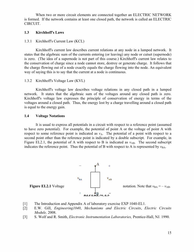
15
When two or more circuit elements are connected together an ELECTRIC NETWORK is formed If the network contains at least one closed path the network is called an ELECTRIC CIRCUIT 13 Kirchhoffs Laws 131 Kirchhoffs Current Law (KCL)
Kirchhoffs current law describes current relations at any node in a lumped network It states that the algebraic sum of the currents entering (or leaving) any node or cutset (supernode) is zero (The idea of a supernode is not part of this course) Kirchhoffs current law relates to the conservation of charge since a node cannot store destroy or generate charge It follows that the charge flowing out of a node exactly equals the charge flowing into the node An equivalent way of saying this is to say that the current at a node is continuous 132 Kirchhoffs Voltage Law (KVL)
Kirchhoffs voltage law describes voltage relations in any closed path in a lumped network It states that the algebraic sum of the voltages around any closed path is zero Kirchhoffs voltage law expresses the principle of conservation of energy in terms of the voltages around a closed path Thus the energy lost by a charge travelling around a closed path is equal to the energy gain 14 Voltage Notations
It is usual to express all potentials in a circuit with respect to a reference point (assumed to have zero potential) For example the potential of point A or the voltage of point A with respect to some reference point is indicated as vA The potential of a point with respect to a second point other than the reference point is indicated by a double subscript For example in Figure EL21 the potential of A with respect to B is indicated as vAB The second subscript indicates the reference point Thus the potential of B with respect to A is represented by vBA
Figure EL21 Voltage notation Note that vBA = ndash vAB REFERENCES [1] The Introduction and Appendix A of laboratory exercise EXP 1040-EL1 [2] EW Gill Engineering1040 Mechanisms and Electric Circuits Electric Circuits Module 2008 [3] S Wolf and R Smith Electronic Instrumentation Laboratories Prentice-Hall NJ 1990
16
20 PRELAB 21 Read Section 1 of EXP 1040-EL1 and pages 13ndash26 of Reference [2] 22 Determine the colour coding for each of the following resistors
i) 820 kΩ ii) 1 kΩ iii) 68 MΩ iv) 18 MΩ 23 Consider the circuit of Figure EL22
i) Write the Kirchhoffrsquos voltage law equations for loops adba and adcba ii) Write the Kirchhoffrsquos current law equations for nodes d and c iii) Use the four equations in (i) and (ii) to find the currents i1 i2 i3 and i4 iv) Find the voltages across the resistors having the polarities shown in the figure v) Determine the power dissipated by each resistor vi) Find the power supplied by the source and compare with the total power
developed in the circuit 24 In Figure EL22 determine the equivalent resistance seen by the voltage source ie the
input resistance of the circuit given by Rin = vABi1 25 Troubleshooting is the process of identifying and locating a failure (fault) or problem in a
circuit Generally the problems are due to open circuits or short circuits Consider the circuit of Figure EL22 A DMM set to measure the voltage across R4 reads vCB = 228 V Determine if there is a fault in the circuit If there is a fault identify it as either a short or open circuit
30 APPARATUS AND MATERIALS
1 Fluke 8010A Digital Multimeter (DMM) 1 Sun Equipment Powered Breadboard Model PBB-4060B Standard Resistors 2times100 Ω 150 Ω 220 Ω One set of leads with banana plugs and alligator clips Various connecting wires
40 EXPERIMENT 41 RESISTANCE MEASUREMENT USING THE DMM 411 With the DMM set to measure RESISTANCE measure and record in Table 1 the
resistance of each resistor in the circuit of Figure EL22 Note that the resistance of each resistor must be measured separately Also record the standard values
412 Construct the circuit of Figure EL22 on the breadboard provided Do not connect the
voltage source to the circuit With the DMM set to read RESISTANCE connect the DMM to nodes a and b and record the equivalent resistance of the resistive circuit as Rin in Table 1 Also record in Table 1 Rin calculated using the values measured in 411
17
vab = +8 V R1 = 100 Ω R2 = 220 Ω R3 = 150 Ω R4 = 100 Ω
Figure EL22 Series-parallel circuit for analysis and experimentation
42 VOLTAGE AND CURRENT MEASUREMENTS USING THE DMM 421 Connect the voltage source to the resistive circuit at points a (red lead) and b (black lead)
Set the DMM to read dc volts and adjust the 0 to 16 V voltage source from the breadboard to give a +8 V dc reading on the DMM Record this as vab in Table 1 Note It may not be possible to adjust the source to read exactly +8 V ndash simply record the closest value that you are able to obtain
422 Recall the voltage measurement technique from the information given in Lab 1 Measure and record in Table 1 the dc voltages across the resistors in the circuit of Figure EL22
with the polarities as specified Set the DMM on the most appropriate range for these measurements
423 Recall the current measurement technique from the information given in Lab 1 With the
DMM set on dc amps measure the current flowing in each resistor with the directions specified in Figure EL22 Record the results in the Table 1
424 Using the measured quantities calculate the power dissipated by each resistor Record
the results in Table 1 425 Compare the measured (or lsquostandardrsquo in case of the resistors) and calculated results of the
resistances currents voltages and power Comment on the results 426 From the results for the measured voltages in Table 1 verify that (within expected errors)
KVL has been satisfied for (i) mesh adba (ii) loop adcba and (iii) mesh dcbd Briefly discuss any discrepancy Note a mesh is a loop that does not contain any other loop(s) For example in this circuit loop adcba contains mesh adba and mesh dcbd
18
427 From the results for the measured currents in Table 1 verify that (within expected errors) KCL has been satisfied for (i) node d and (ii) node c Briefly discuss any discrepancy
428 Verify that the power delivered by the voltage source is equal to the total power
dissipated by the resistors 43 TROUBLESHOOTING 431 Verify the troubleshooting problem in Section 25 432 Provide an analysis of the problem and discuss the conceptual basis for identifying the
type of fault 50 CONCLUSIONS
19
TABLE 1 ndash Resistance Current and Voltage Measurements
ParameterVariable
Standard or Calculated
Measured
R1 (Ω)
R2 (Ω)
R3 (Ω)
R4 (Ω)
Rin (Ω)
vab (V)
v1 (V)
v2 (V)
v3 (V)
v4 (V)
i1 (mA)
i2 (mA)
i3 (mA)
i4 (mA)
P1 (W)
P2 (W)
P3 (W)
P4 (W)
Pdev (W)
Pdiss (W)
20
APPENDIX A (Modified from the former Engineering 1333 Lab manual by Dr John Quaicoe)
This appendix contains several important ideas that will be useful in any of your encounters with real electric circuits In reality measurements in a circuit will depend on all elements of the circuit and all connectors as well as on the operating conditions A1 Resistors
The flow of charge through any material encounters an opposing force This opposition due to the collisions between electrons and between electrons and other atoms in the material which converts electrical energy into heat is called the resistance of the material A device specifically designed to have resistance is called a resistor A11 Factors Which Affect Resistance
The resistance of any material with a uniform cross sectional area depends on the material used the length the cross-sectional area and temperature under which operation occurs Conductor Length and Cross Sectional Area
If the effects of temperature are neglected resistance depends directly on the length of the material and inversely on the cross-sectional area In equation form the resistance of a conductor at room temperature of 20oC is expressed as R = ρlA (A1) where R is the resistance in ohms
l is the length in metres or feet A is the cross-sectional area in m2 or circular mils (CM) ρ is the resistivity or specific resistance in Ωmiddotm or ΩmiddotCMft
Electrical conductors are generally circular in cross-section with wire diameters measured
in mils 1 mil = 11000 in = 10-3 in (A2) The cross-sectional area of a conductor is for convenience defined in circular mils The circular mil is the area of a circular cross-section having a diameter of 1 mil Area (circle) = πd24 (A3) Since the area depends on the square of the diameter for any arbitrary diameter d in mils the area in circular mils is given by A = d2 cir mils (CM) (A4)
It is still quite common to define the resistivity in the Imperial (English) system as the resistance of a 1 ft length of conductor with an area of 1 CM Of course the SI unit for
21
resistivity as is easily deduced from equation (A1) will be the Ωmiddotm Table A1 lists resistivity values of common conducting materials in both SI and Imperial units
Table A1 The resistivities of common conducting materials at 20oC
Conducting Material
Resistivity (Ωm)
Resistivity (Ωcir milft)
Aluminum
283 x 10-8
170
Brass
7 x 10⁻⁸
420
Copper annealed
172 x 10-8
1037
Copper hard-drawn
178 x 10-8
107
Gold
245 x 10-8
147
Lead
221 x 10-8
132
Nichrome
100 x 10-8
600
Platinum
10 x 10-8
602
Silver
164 x 10-8
99
Tin
115 x 10-8
692
Tungsten
552 x 10-8
332
Zinc
623 x 10-8
374
Examples 1 An annealed copper bar measures 1 x 3 cm and is 12 m long What is the resistance
between the ends of the bar
Solution R = ρlA = (172 x 10-8) x (5 x 10-1)(1 x 10-2 x 3 x 10-2)
= 285 x 10-5 Ω
2 Find the resistance of an annealed copper wire 200 ft long with a 100 mil diameter
Solution A(cir mil) = d2 = (100)2 = 104 CM R = ρlA = (1037) x (200)104 = 207 x 10ndash2 Ω
22
Temperature Effects
For most conductors as the temperature increases either from current flowing through it or by heat absorption from the surrounding medium the resistance increases This is due to the increased molecular movement within the conductor which hinders the flow of charge The resistance increases almost linearly with increase in temperature
The relationship between temperature and resistance is expressed as (|T| + t1)R1 = (|T| +t2)R2 (A5) where |T| is the inferred absolute zero of the material involved in oC R1 is the resistance of the material at the temperature t1
oC R2 is the resistance of the material at the temperature t2
oC
The relationship between temperature and resistance may be expressed by
R2 = R1 [1 + α1(t2 - t1)] (A6) where α1 is the temperature coefficient of resistance
R1 is the resistance at the temperature t1 and
R2 is the resistance at the temperature t2
Table A2 lists the inferred absolute zero and temperature coefficients of common conducting materials
Most materials exhibit an increase in resistance with an increase of temperature and are said to have a positive temperature coefficient of resistance However some materials such as carbon and semiconductor materials exhibit a decrease in resistance with an increase of temperature and are said to have a negative temperature coefficient of resistance Examples 1 What is the resistance of an annealed copper wire at 10oC if the resistance is 50 Ω at
60oC
Solution (|T| + t1)R1 = (|T| +t2)R2 t2 = 60o R2 = 50 Ω |T| = 2345o
t1 = 10oC R1 =
R1 = (|T| + t1) R2 (|T| + t2)
= 50 x (2445)(2945) = 415 Ω
23
2 What is the resistance of a copper wire at 10oC if the resistance at 20oC is 433 Ω and if
α1 = 000393
Solution
R2 = R1(1 + α1 ΔT)
= 433 [1 + 000393 (10-20)] = 416 Ω
Table A2 Inferred absolute zero and temperature coefficients for common conducting materials
Conducting
Material
Inferred Absolute zero (C)
Temperature coefficient (Ω CΩ at 0oC)
Aluminum
-236
000424
Brass
-480
000208
Copper annealed
-2345
000427
Copper hard drawn
-242
000413
Gold
-274
000365
Lead
-224
000466
Nichrome
-2270
000044
Platinum
-310
000323
Silver
-243
000412
Tin
-218
000458
Tungsten
-202
000495
Zinc
-250
000400
24
A1 2 Wire Tables [3] Circular cross-section wire is designed by a gauge size of number representing a certain diameter wire The wire table is designed primarily to standardize the size of wire produced by manufacturers The American Wire Gauge (AWG) sizes are given in Table A3 Note that the larger the gauge number the smaller the diameter of the conductor
Table A3 American Wire Gauge (AWG) Sizes of Copper Wire [3]
APPLICATIONS
AWG
AREA (CM)
Ω1000 ft (200 C)
Max Current
(900 C) Power distribution
00
133100
0078
186
1
83690
0124
137
4
41470
0240
89
House main power carriers
6
26240
0395
65
8
16510
0620
48
Lighting outlets general home use
12
6530
1588
20
14
4110
252
15
Television radio
20
10215
101
-
22
6424
161
-
Telephone instruments
28
1598
649
-
35
315
3290
-
40
99
10490
-
An examination of the table shows that if the gauge number changes by 10 the cross-
sectional area changes by approximately a factor of 10 Thus the resistance also changes by approximately 10 times For example AWG 4 has a cross-sectional area of 41470 CM and resistance of 0240 Ω1000 ft whereas AWG 14 has a cross-sectional area of 4110 CM and a resistance of 252 Ω1000 ft ie an increase of 10 in the gauge number represents a decrease in the area by a factor of approximately 10 and an increase in the resistance by a factor of approximately 10 A13 Types of Resistors
Resistors are used for many purposes and are therefore made in many forms The most common of the resistor types are the carbon composition resistor the wirewound resistor the
25
metal film resistor and the carbon film resistor They all belong in either of two groups fixed or variable
The most common of the low-wattage fixed-type resistors is the carbon composition resistor It is made of hot-pressed carbon granules mixed with varying amounts of binding material to achieve a large range of resistance values They are used extensively in electronic applications They are relatively inexpensive reliable and free of stray capacitance and inductance They are available in power ratings up to 2W with resistance values in the range of 1 to 22 MΩ and 5 to 20 tolerance The resistance value of carbon composition resistors and tolerances are specified by a set of colour-coded bands painted on the resistor body Each colour represents a digit in accordance with Figure A1 in the appendix of Exp 1040-EL1 The resistance value as indicated by the colour bands of carbon composition resistors is called the nominal value of resistance Wire wound resistors are commercially available for high precision low resistance and high power dissipation applications They usually consist of Nichrome or copper-nickel wire wound on a ceramic tube and protected from mechanical and environmental hazards by a protective coating of vitreous enamel or silicone Their resistance values range from 1Ω to 100 kΩ with a tolerance range of 00005 and above and a maximum power rating of 200 W
A third group of resistors consist of a thin film of material deposited on insulating materials to provide very high resistance paths Depending on the material used the resistors are classified as carbon film metal film or metal-oxide film resistors Their values range up to 10000 MΩ
Variable resistors come in many forms but basically they can be separated into the linear or non-linear types Variable resistors usually have three leads two fixed and one moveable If contacts are made to only two leads of the resistor the variable resistor is being employed as a rheostat If all three contacts are used in a circuit it is termed as potentiometer or pot The value of the overall resistance and the power ratings of variable resistors are usually stamped on their cases Because the resistance of a conducting film varies with length cross-section and temperature it is possible to use resistance measurement to sense changes in any of those parameters A device that responds to one physical effect is called a transducer Electrical transducers are often used in instrumentation for non-electrical quantities such as temperature light and strain The resistance of the device can be measured and the magnitude of the physical or chemical parameter inferred from the resistance value Typical examples of resistive transducers are 1 The thermistor a two-terminal semiconductor device designed specifically to exhibit a
change in electrical resistance with a change in its body temperature 2 The strain gauge a device which converts linear dimension changes into resistive
changes 3 The photoconductive cell a two-terminal device whose resistance depends upon the
intensity of light impinging on the cell
EXP 1040-EL3 Applications of Resistive Networks PURPOSE To (1) investigate the idea of voltage division using a single source and (2) to examine the utility of a Wheatstone bridge circuit for resistance measurements 10 INTRODUCTION
Using the laws discussed in the course material ndash namely Ohmrsquos law Kirchhoffrsquos Voltage Law (KVL) and Kirchhoffrsquos Current Law (KCL) ndash we are now in a position to study many different circuits having a variety of real-world applications In this lab we consider two such applications and while the analysis associated with them is relatively straight forward they are of significant modern-day importance 11 Voltage Divider Circuits
A voltage source is sometimes required to supply a particular voltage to a load and in fact it may be required to supply several loads with certain specified voltages simultaneously Ideally the voltage supplied should not depend on the size of the load
As a first example consider the circuit shown in Figure EL31 in which a simple voltage
divider circuit is connected in series with the load Notice the situation has been depicted in two equivalent ways In the second schematic the negative terminal of the source is assumed to be electrical ground An electrical ground is a reference level from which other voltages are measured An ideal electrical ground can absorb an unlimited amount of current without changing its potential Here then conventional current flows from the positive terminal of the source through the resistors and back to the source via the ground path (the closed path connection is not explicit in the schematic diagram but it is understood)
Figure EL31 Two equivalent schematics (a) and (b) for a simple voltage divider
From Section E251 of the class notes Electric Circuits Module we know that
⎥⎦
⎤⎢⎣
⎡+
=Ls
LsL RR
Rvv (1)
26
However this type of voltage divider has a serious disadvantage since the value of vL depends on the value of iL and the latter will change depending on the value of the load resistance
To help overcome the problem referred to above it is possible to construct a voltage divider with a bleeder resistor RB as shown below in Figure EL32 and as discussed in Section 251 (page 29) of the class notes Electric Circuits Module
Figure EL32 Two representations (a) and (b) of a voltage divider with a bleeder resistor Strictly the voltage across the parallel section of the circuit is (by the voltage divide lsquorulersquo)
⎥⎦
⎤⎢⎣
⎡+
=)||(
||
BS
LBsL
LRRRRRvv (2)
where
⎥⎦
⎤⎢⎣
⎡+
=LRR
RRRRB
LBLB || (3)
As shown in the class notes the advantage of this kind of voltage division is that when RBltltRL the load voltage is essentially independent of the load resistance and
⎥⎦
⎤⎢⎣
⎡+
=BS
BsL RR
Rvv (4)
Because the load voltage is less affected by the load resistance in this situation we say there is better voltage regulation in this circuit than that in Figure EL31 12 The Wheatstone Bridge The Wheatstone bridge circuit is mainly used to measure an unknown resistance However the principle of the Wheatstone bridge is used in many transducers ndash devices that convert one kind of energy into another ndash and instrumentation systems to measure a physical variable such as 27
strain temperature and pressure A Wheatstone bridge circuit is shown in Figure EL33 In this figure R3 is a variable resistance which models the transducer If a change in physical variable results in a change in resistance of the transducer the Wheatstone bridge can be used to convert the change in resistance to a change in voltage which can be measured
Figure EL33 A Wheatstone bridge
When the voltage vab is zero the bridge is said to be balanced If two resistances (say R1 and R2) are known and another (say Rx) is unknown then a fourth adjustable known resistance R3 (potentiometer) can be used to determine the unknown resistance Rx under balanced conditions When R3 is actually a transducer whose resistance changes with some change in a physical parameter such as temperature then if R1 R2 and Rx are known the voltage vab is an indicator of the size of the measured parameter Balanced Conditions As noted for balanced conditions the voltage vab is zero Also under these conditions using the voltage divide rule twice gives
⎥⎦
⎤⎢⎣
⎡+
=x1
x
RRRvvad (5)
⎥⎦
⎤⎢⎣
⎡+
=32
3
RRRvvbd (6)
We have also seen from Section 254 of the Electric Circuits Module lecture notes that
32
1x R
RRR ⎟⎟
⎠
⎞⎜⎜⎝
⎛= (7)
Unbalanced Conditions When the bridge is not balanced ndash ie vab ne 0 ndash then using Kirchhoffrsquos laws it is straight forward to show that
⎥⎦
⎤⎢⎣
⎡+
minus+
=32
3
x1
x
RRR
RRRvvab (8)
28
29
From this equation we see immediately that if any three of the resistances are fixed in value then a change in the other resistance results in a change in vab Thus a variation in vab is effectively a measure of a change in the variable resistance REFERENCES [1] The Introduction and Appendix A of laboratory exercise EXP 1040-EL1 [2] EW Gill Engineering1040 Mechanisms and Electric Circuits Electric Circuits Module 2008 20 PRELAB 21 Carefully read Section 1 (Introduction) of this experiment and the sections referred to in reference [2] 22 Refer to Figure EL31 The series dropping resistor has a value of 10 kΩ (a) Determine the value of the load resistor RL so that vL = 75 V if the source voltage is 10 V (b) If the load resistance is increased by 25 calculate the new vL 23 Refer to Figure EL32 (a) Design a voltage divider (ie find Rs and RB) for the load
resistance RL obtained in part (a) of Question 22 so that it can operate at vL = 75 V from a 10 V source Assume that the bleeder current iB is 75 mA (b) If the load resistance is increased by 25 calculate the new load voltage Compare this result with that obtained in Question 22 (b) Comment on the comparison
30 APPARATUS AND MATERIALS
1 Fluke 8010A Digital Multimeter (DMM) 1 Sun Equipment Powered Breadboard Model PBB-4060B Standard Resistors 1 kΩ 3 times 120 Ω others as calculated in design Potentiometers 200 Ω 5 k Ω One set of leads with banana plugs and alligator clips and various connecting wires
40 EXPERIMENT 41 Voltage Divider 411 Familiarize yourself with potentiometers ndash the lab attendants will help On the breadboard construct the voltage divider circuit as shown in Figure EL31 using a 1 kΩ resistor for Rs and a 5 k Ω potentiometer (variable resistor) as the load resistor RL Ensure that the source voltage is 10 V after connecting to the circuit Adjust the variable resistor to get an output (load) voltage of vL = 75 V Measure the value of RL for this condition Comment on any discrepancies between the measured and calculated value in Question (22) of the Prelab
30
412 Vary the potentiometer resistance from 680 Ω to 5 k Ω and obtain the load voltage vL in each case Tabulate your results and plot vL as a function of RL 413 Construct the voltage divider found in Figure EL32 and measure the load voltages to
verify your design of Question 23 of the Prelab Use the nearest available resistance values to those you calculated in the design Comment on your findings
42 Wheatstone Bridge 421 On the breadboard construct the Wheatstone bridge circuit of Figure EL33 using three
120 Ω (nominal) resistors for R1 R2 and Rx and a 200 Ω potentiometer (pot) for R3 Also measure and record the actual values of the 120 Ω resistors Ensure that the source voltage v is 10 V after it is connected to the circuit Use the DMM as a voltmeter in the branch between nodes a and b
422 Adjust the pot until the bridge is balanced Measure and record the value of R3 for this
condition Confirm your observation by calculating R3 from equation (7) and comment on any discrepancies
50 DISCUSSION 51 Comment on probable applications of a voltage divider circuit 52 Discuss any technical difficulties encountered during the lab
_____________________________________________________________________________ EXP 1040-DL1 Introduction to Logic Gates and Ladder Diagrams PURPOSE To (i) familiarize the student with the basic logic gates AND OR NOT and NAND (ii) implement basic logic gates using relay logic and (iii) learn how to represent logic circuits by means of ladder diagrams 10 INTRODUCTION Logic circuits may be implemented (constructed) in a variety of ways perhaps most commonly today via electronic components In this lab and the next however we consider the implementation of basic logic expressions using a simple circuit board in conjunction with a few pneumatic cylinders This allows us to explore basic logic circuits without having to resort to sophisticated solid state circuitry (transistors etc) 20 PRELAB There is no prelab for this session However students need to read Section D13 pages 10-18 of the Digital Logic Module before the lab session 30 APPARATUS AND MATERIALS 1 Logic Board Various banana plug connectors AC power (from main lab supply) 40 EXPERIMENT
41 Board Familiarization 411 Normally-open Switch To gain familiarity with the laboratory test panel implement the simple circuit shown in Figure DL11 PB1 refers to one of the two push buttons available on the panel This specific circuit utilizes a ldquonormally openrdquo contact When PB1 is pressed the green indicator light should illuminate
31
CGreenPB1
24V N
Figure DL11 Simple circuit employing push button and a green indicator light
412 Normally-closed Switch Repeat exercise 411 using the ldquonormally closedrdquo contact of PB1 See Figure DL12
CGreen
24V N
PB1
Figure DL12 Simple circuit employing a normally closed contact
42 AND Gate
Using the two push buttons PB1 and PB2 implement an AND operation In other words the green indicator light should only illuminate if and only if both buttons are pressed simultaneously In your lab report provide
bull the ladder diagram implementation (similar to Figure DL11 or DL12) bull the standard symbol for a two input AND gate bull The truth table Note that the truth table should include all four combinations
of the two inputs Assume that a high or logic ldquo1rdquo occurs when the button is pressed
bull Provide a practical application of this circuit (hint think safety)
32
43 OR Gate
Repeat part 42 above in its entirety however this time implement an OR operation using the two push buttons PB1 and PB2 In this case the green indicator should illuminate if at least one of the two buttons is pressed For the practical application consider convenience instead of safety
44 OR Gate
Repeat part 42 above for a ldquoNANDrdquo gate Note that this will require normally closed contacts It is not necessary to provide a practical application for this circuit
45 NOR Gate
Repeat part 42 above for a NOR gate Note that this will require normally closed contacts It is not necessary to provide a practical application for this circuit
46 Inequality Comparator Figure DL13 represents a circuit that is sometimes referred to as an inequality comparator Implement the circuit and experimentally determine the truth table Note that this circuit employs both the ldquonormally openedrdquo and ldquonormally closedrdquo contacts of both push buttons In the lab report provide both the common name for this circuit as well as the standard logic symbol Why is this circuit referred to as an ldquoinequality comparatorrdquo
CGreen
24V N
PB1 PB2
PB_2PB_1
Figure DL13 Circuit that implements an ldquoinequality comparatorrdquo
47 Inverter
An inverter or NOT gate can be implemented with a relay as shown in Figure DL14 When the push button is pressed the coil of relay 1 is energized This opens the normally closed contact of relay 1 which turns the Green indicator light off Implement the circuit and experimentally determine the operation In the lab report provide the standard logic symbol for a NOT gate
33
CR1
24V N
PB2
R_1C
Green
Figure DL14 Circuit that implements a NOT gate
48 Latch (Priority on Set)
A relay can also be used to ldquolatchrdquo the state of the output such that the indicator light is illuminated when the push button is pressed and stays illuminated even if the button is released A second push button must be used to reset the circuit back to its initial (ldquoOFFrdquo) state In Figure DL15 PB1 energizes relay 1 when it is pressed One of the sets of contacts on relay 1 is used to maintain the relay energized even if PB1 is released The normally closed contact of button PB2 de-energizes the relay when the button is pressed (ie resets the latch) Implement the circuit and experimentally determine the operation Be sure and verify what happens when both buttons are pressed simultaneously Note that you must use a different set of relay contacts to energize the green indicator light This particular latching configuration is referred to as priority on SET
CR1
24V N
PB1
PB2
CGreen
R_1
R__1
Figure DL15 Implementation of a ldquolatchrdquo circuit using a relay
34
49 Latch (Priority on Re-Set)
An alternative latch configuration is implemented in Figure DL16 This configuration is referred to as priority on RESET Implement the circuit and experimentally determine the operation Be sure and verify what happens when both buttons are pressed simultaneously In terms of operation what is the main difference between ldquopriority on SETrdquo and ldquopriority on RESETrdquo Provide a practical application of both latch configurations (once again think safety)
CR1
24V N
PB1 PB2
CGreen
R_1
R__1
Figure DL16 Implementation of ldquopriority on RESETrdquo
35
_____________________________________________________________________________ EXP 1040-DL1 Introduction to Sequential Circuits Ladder Diagrams and Relay Logic PURPOSE To (i) introduce ladder diagrams and relay logic and (ii) demonstrate a simple pneumatic system 10 INTRODUCTION Ladder Diagrams (Figure DL21) are a graphical representation of sequential control circuits that are widely used in industry Although originally intended as a way of representing relay logic ladder diagrams are now the standard means of programming microprocessor based PLCs (Programmable Logic Controllers) They are prevalent in a many engineering fields including automation process control and manufacturing In this lab a sequential logic circuit will be implemented using the pneumatic test board The pneumatic test board has three pneumatic cylinders that are activated by solenoid valves The position of each cylinder is monitored by two limit switches One limit switch is activated when the cylinder is fully extended and the other is activated when the cylinder is fully retracted By energizing a solenoid you are able to extend a cylinder and by de-energizing the solenoid the cylinder will retract 20 PRELAB There is no prelab for this session However students need to read Unit D2 of the Digital Logic Module before the lab session 30 APPARATUS AND MATERIALS 1 Logic Board Various banana plug connectors AC power (from main lab supply) Compressed air source 40 EXPERIMENT
41 Limit Switch Familiarization
36
Limit switches A0 and A1 in Figure DL21 are used to sense when cylinder A is retracted and extended respectively Each switch incorporates both a normally opened and normally closed set of contacts Cylinders B and C employ switched B0 B1 and C0C1 respectively These six switches are identified on the wiring panel as S1 through S6 An indicator light can be used to verify the operation of the switches Sketch a circuit that illuminates the green light when cylinder A extends and the red light when cylinder A retracts Implement the circuit on the pneumatic test board and verify the operation by manually depressing the limit switches Use the circuit to determine the correspondence between the six limit switches and the wiring terminals S1 through S6
Figure DL21 Ladder diagram (left) for controlling two pneumatic cylinders 42 Solenoid Valve Familiarization
Solenoid valves S1 S2 and S3 control the three cylinders A B and C As shown in Figure DL21 when the solenoid valves are not energized the cylinders are retracted ie pressure is applied to the rod side of the cylinder Energizing the solenoid changes the position of the valve such that the cap side of the cylinder is pressurized and the
37
38
cylinder extends Sketch a circuit that extends cylinder A when push button PB1 is depressed and retracts A when the button is released Implement the circuit on the pneumatic test board and verify the operation There are a many ldquopinchrdquo points on the test board so be sure and keep your fingers away from the cylinders
43 Implementation of a Simple Latch
Using relay 1 design a circuit that latches the state of push button PB1 such that cylinder A extends when PB1 is depressed and stays extended even if PB1 is released The cylinder retracts only when push button PB2 is depressed Implement the circuit on the pneumatic test board and verify the operation
44 Sequential Logic Circuit 1 441 Familiarization with the Logic Sequence
The ladder diagram shown in Figure DL21 is a sequential logic circuit that will make two cylinders follow the sequence Cylinder A ndash extend -gt Cylinder B ndash extend -gt Cylinder A ndash retract -gt Cylinder B ndash retract The operation of the logic circuit can be described as follows
bull Push button PB1 initiates the start of the sequence ie extend cylinder A by activating solenoid A Relay 2 is latched when PB1 is depressed if and only if the last step in the sequence (limit switch B0 retract B) has been completed This also maintains solenoid A energized bull Once cylinder A has finished extending (ie switch A1 is active) the circuit advances to the second ldquorungrdquo of the ladder which activates solenoid B (cylinder B extends) bull When switch B1 is activated (ie B extended) the circuit advances to the third rung in the ladder Relay 4 is latched which in turn resets relay 2 de-energizing Solenoid A and retracting A bull In a similar fashion the fourth rung in the ladder resets relay 3 which retracts B bull Notice that each rung in the ladder is latched by the completion of the action associated with the previous rung
442 Implementation of the Logic Sequence
Implement the circuit described in 441 and verify the operation
45 Sequential Logic Circuit 2
Modify the circuit in section 44 to implement the following sequence
39
Cylinder A ndash extend -gt Cylinder B ndash extend -gt Cylinder B ndash retract -gt Cylinder A ndash retract
5 Lab Report 51 Provide a short written lab report that includes ladder diagrams of all the circuits design during the lab
52 Explain the operation of the circuit developed in part 45 above
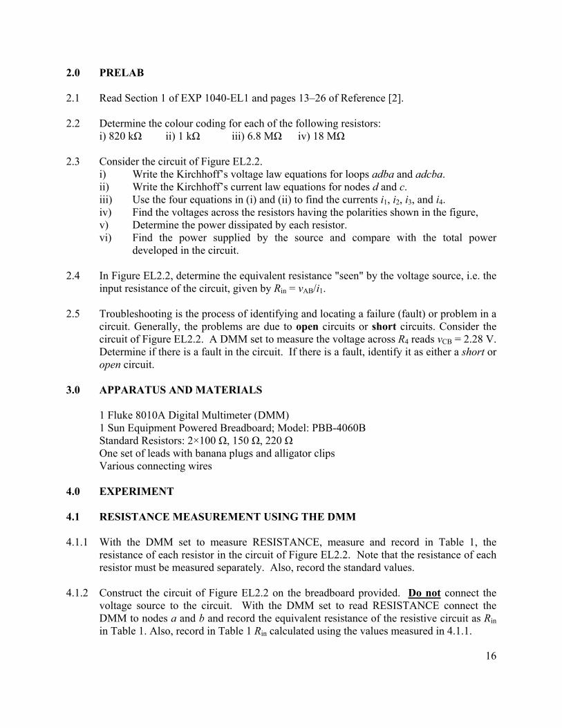
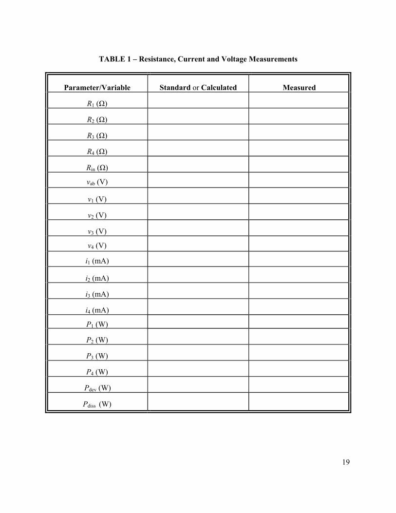
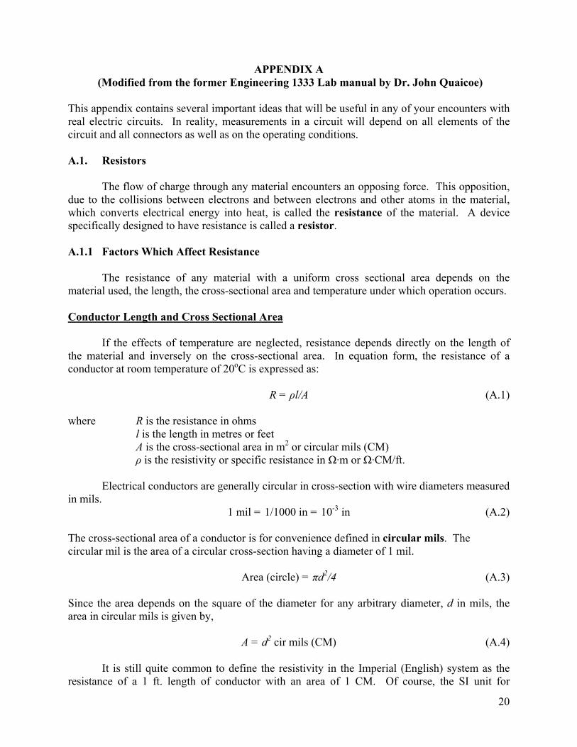
20
APPENDIX A (Modified from the former Engineering 1333 Lab manual by Dr John Quaicoe)
This appendix contains several important ideas that will be useful in any of your encounters with real electric circuits In reality measurements in a circuit will depend on all elements of the circuit and all connectors as well as on the operating conditions A1 Resistors
The flow of charge through any material encounters an opposing force This opposition due to the collisions between electrons and between electrons and other atoms in the material which converts electrical energy into heat is called the resistance of the material A device specifically designed to have resistance is called a resistor A11 Factors Which Affect Resistance
The resistance of any material with a uniform cross sectional area depends on the material used the length the cross-sectional area and temperature under which operation occurs Conductor Length and Cross Sectional Area
If the effects of temperature are neglected resistance depends directly on the length of the material and inversely on the cross-sectional area In equation form the resistance of a conductor at room temperature of 20oC is expressed as R = ρlA (A1) where R is the resistance in ohms
l is the length in metres or feet A is the cross-sectional area in m2 or circular mils (CM) ρ is the resistivity or specific resistance in Ωmiddotm or ΩmiddotCMft
Electrical conductors are generally circular in cross-section with wire diameters measured
in mils 1 mil = 11000 in = 10-3 in (A2) The cross-sectional area of a conductor is for convenience defined in circular mils The circular mil is the area of a circular cross-section having a diameter of 1 mil Area (circle) = πd24 (A3) Since the area depends on the square of the diameter for any arbitrary diameter d in mils the area in circular mils is given by A = d2 cir mils (CM) (A4)
It is still quite common to define the resistivity in the Imperial (English) system as the resistance of a 1 ft length of conductor with an area of 1 CM Of course the SI unit for
21
resistivity as is easily deduced from equation (A1) will be the Ωmiddotm Table A1 lists resistivity values of common conducting materials in both SI and Imperial units
Table A1 The resistivities of common conducting materials at 20oC
Conducting Material
Resistivity (Ωm)
Resistivity (Ωcir milft)
Aluminum
283 x 10-8
170
Brass
7 x 10⁻⁸
420
Copper annealed
172 x 10-8
1037
Copper hard-drawn
178 x 10-8
107
Gold
245 x 10-8
147
Lead
221 x 10-8
132
Nichrome
100 x 10-8
600
Platinum
10 x 10-8
602
Silver
164 x 10-8
99
Tin
115 x 10-8
692
Tungsten
552 x 10-8
332
Zinc
623 x 10-8
374
Examples 1 An annealed copper bar measures 1 x 3 cm and is 12 m long What is the resistance
between the ends of the bar
Solution R = ρlA = (172 x 10-8) x (5 x 10-1)(1 x 10-2 x 3 x 10-2)
= 285 x 10-5 Ω
2 Find the resistance of an annealed copper wire 200 ft long with a 100 mil diameter
Solution A(cir mil) = d2 = (100)2 = 104 CM R = ρlA = (1037) x (200)104 = 207 x 10ndash2 Ω
22
Temperature Effects
For most conductors as the temperature increases either from current flowing through it or by heat absorption from the surrounding medium the resistance increases This is due to the increased molecular movement within the conductor which hinders the flow of charge The resistance increases almost linearly with increase in temperature
The relationship between temperature and resistance is expressed as (|T| + t1)R1 = (|T| +t2)R2 (A5) where |T| is the inferred absolute zero of the material involved in oC R1 is the resistance of the material at the temperature t1
oC R2 is the resistance of the material at the temperature t2
oC
The relationship between temperature and resistance may be expressed by
R2 = R1 [1 + α1(t2 - t1)] (A6) where α1 is the temperature coefficient of resistance
R1 is the resistance at the temperature t1 and
R2 is the resistance at the temperature t2
Table A2 lists the inferred absolute zero and temperature coefficients of common conducting materials
Most materials exhibit an increase in resistance with an increase of temperature and are said to have a positive temperature coefficient of resistance However some materials such as carbon and semiconductor materials exhibit a decrease in resistance with an increase of temperature and are said to have a negative temperature coefficient of resistance Examples 1 What is the resistance of an annealed copper wire at 10oC if the resistance is 50 Ω at
60oC
Solution (|T| + t1)R1 = (|T| +t2)R2 t2 = 60o R2 = 50 Ω |T| = 2345o
t1 = 10oC R1 =
R1 = (|T| + t1) R2 (|T| + t2)
= 50 x (2445)(2945) = 415 Ω
23
2 What is the resistance of a copper wire at 10oC if the resistance at 20oC is 433 Ω and if
α1 = 000393
Solution
R2 = R1(1 + α1 ΔT)
= 433 [1 + 000393 (10-20)] = 416 Ω
Table A2 Inferred absolute zero and temperature coefficients for common conducting materials
Conducting
Material
Inferred Absolute zero (C)
Temperature coefficient (Ω CΩ at 0oC)
Aluminum
-236
000424
Brass
-480
000208
Copper annealed
-2345
000427
Copper hard drawn
-242
000413
Gold
-274
000365
Lead
-224
000466
Nichrome
-2270
000044
Platinum
-310
000323
Silver
-243
000412
Tin
-218
000458
Tungsten
-202
000495
Zinc
-250
000400
24
A1 2 Wire Tables [3] Circular cross-section wire is designed by a gauge size of number representing a certain diameter wire The wire table is designed primarily to standardize the size of wire produced by manufacturers The American Wire Gauge (AWG) sizes are given in Table A3 Note that the larger the gauge number the smaller the diameter of the conductor
Table A3 American Wire Gauge (AWG) Sizes of Copper Wire [3]
APPLICATIONS
AWG
AREA (CM)
Ω1000 ft (200 C)
Max Current
(900 C) Power distribution
00
133100
0078
186
1
83690
0124
137
4
41470
0240
89
House main power carriers
6
26240
0395
65
8
16510
0620
48
Lighting outlets general home use
12
6530
1588
20
14
4110
252
15
Television radio
20
10215
101
-
22
6424
161
-
Telephone instruments
28
1598
649
-
35
315
3290
-
40
99
10490
-
An examination of the table shows that if the gauge number changes by 10 the cross-
sectional area changes by approximately a factor of 10 Thus the resistance also changes by approximately 10 times For example AWG 4 has a cross-sectional area of 41470 CM and resistance of 0240 Ω1000 ft whereas AWG 14 has a cross-sectional area of 4110 CM and a resistance of 252 Ω1000 ft ie an increase of 10 in the gauge number represents a decrease in the area by a factor of approximately 10 and an increase in the resistance by a factor of approximately 10 A13 Types of Resistors
Resistors are used for many purposes and are therefore made in many forms The most common of the resistor types are the carbon composition resistor the wirewound resistor the
25
metal film resistor and the carbon film resistor They all belong in either of two groups fixed or variable
The most common of the low-wattage fixed-type resistors is the carbon composition resistor It is made of hot-pressed carbon granules mixed with varying amounts of binding material to achieve a large range of resistance values They are used extensively in electronic applications They are relatively inexpensive reliable and free of stray capacitance and inductance They are available in power ratings up to 2W with resistance values in the range of 1 to 22 MΩ and 5 to 20 tolerance The resistance value of carbon composition resistors and tolerances are specified by a set of colour-coded bands painted on the resistor body Each colour represents a digit in accordance with Figure A1 in the appendix of Exp 1040-EL1 The resistance value as indicated by the colour bands of carbon composition resistors is called the nominal value of resistance Wire wound resistors are commercially available for high precision low resistance and high power dissipation applications They usually consist of Nichrome or copper-nickel wire wound on a ceramic tube and protected from mechanical and environmental hazards by a protective coating of vitreous enamel or silicone Their resistance values range from 1Ω to 100 kΩ with a tolerance range of 00005 and above and a maximum power rating of 200 W
A third group of resistors consist of a thin film of material deposited on insulating materials to provide very high resistance paths Depending on the material used the resistors are classified as carbon film metal film or metal-oxide film resistors Their values range up to 10000 MΩ
Variable resistors come in many forms but basically they can be separated into the linear or non-linear types Variable resistors usually have three leads two fixed and one moveable If contacts are made to only two leads of the resistor the variable resistor is being employed as a rheostat If all three contacts are used in a circuit it is termed as potentiometer or pot The value of the overall resistance and the power ratings of variable resistors are usually stamped on their cases Because the resistance of a conducting film varies with length cross-section and temperature it is possible to use resistance measurement to sense changes in any of those parameters A device that responds to one physical effect is called a transducer Electrical transducers are often used in instrumentation for non-electrical quantities such as temperature light and strain The resistance of the device can be measured and the magnitude of the physical or chemical parameter inferred from the resistance value Typical examples of resistive transducers are 1 The thermistor a two-terminal semiconductor device designed specifically to exhibit a
change in electrical resistance with a change in its body temperature 2 The strain gauge a device which converts linear dimension changes into resistive
changes 3 The photoconductive cell a two-terminal device whose resistance depends upon the
intensity of light impinging on the cell
EXP 1040-EL3 Applications of Resistive Networks PURPOSE To (1) investigate the idea of voltage division using a single source and (2) to examine the utility of a Wheatstone bridge circuit for resistance measurements 10 INTRODUCTION
Using the laws discussed in the course material ndash namely Ohmrsquos law Kirchhoffrsquos Voltage Law (KVL) and Kirchhoffrsquos Current Law (KCL) ndash we are now in a position to study many different circuits having a variety of real-world applications In this lab we consider two such applications and while the analysis associated with them is relatively straight forward they are of significant modern-day importance 11 Voltage Divider Circuits
A voltage source is sometimes required to supply a particular voltage to a load and in fact it may be required to supply several loads with certain specified voltages simultaneously Ideally the voltage supplied should not depend on the size of the load
As a first example consider the circuit shown in Figure EL31 in which a simple voltage
divider circuit is connected in series with the load Notice the situation has been depicted in two equivalent ways In the second schematic the negative terminal of the source is assumed to be electrical ground An electrical ground is a reference level from which other voltages are measured An ideal electrical ground can absorb an unlimited amount of current without changing its potential Here then conventional current flows from the positive terminal of the source through the resistors and back to the source via the ground path (the closed path connection is not explicit in the schematic diagram but it is understood)
Figure EL31 Two equivalent schematics (a) and (b) for a simple voltage divider
From Section E251 of the class notes Electric Circuits Module we know that
⎥⎦
⎤⎢⎣
⎡+
=Ls
LsL RR
Rvv (1)
26
However this type of voltage divider has a serious disadvantage since the value of vL depends on the value of iL and the latter will change depending on the value of the load resistance
To help overcome the problem referred to above it is possible to construct a voltage divider with a bleeder resistor RB as shown below in Figure EL32 and as discussed in Section 251 (page 29) of the class notes Electric Circuits Module
Figure EL32 Two representations (a) and (b) of a voltage divider with a bleeder resistor Strictly the voltage across the parallel section of the circuit is (by the voltage divide lsquorulersquo)
⎥⎦
⎤⎢⎣
⎡+
=)||(
||
BS
LBsL
LRRRRRvv (2)
where
⎥⎦
⎤⎢⎣
⎡+
=LRR
RRRRB
LBLB || (3)
As shown in the class notes the advantage of this kind of voltage division is that when RBltltRL the load voltage is essentially independent of the load resistance and
⎥⎦
⎤⎢⎣
⎡+
=BS
BsL RR
Rvv (4)
Because the load voltage is less affected by the load resistance in this situation we say there is better voltage regulation in this circuit than that in Figure EL31 12 The Wheatstone Bridge The Wheatstone bridge circuit is mainly used to measure an unknown resistance However the principle of the Wheatstone bridge is used in many transducers ndash devices that convert one kind of energy into another ndash and instrumentation systems to measure a physical variable such as 27
strain temperature and pressure A Wheatstone bridge circuit is shown in Figure EL33 In this figure R3 is a variable resistance which models the transducer If a change in physical variable results in a change in resistance of the transducer the Wheatstone bridge can be used to convert the change in resistance to a change in voltage which can be measured
Figure EL33 A Wheatstone bridge
When the voltage vab is zero the bridge is said to be balanced If two resistances (say R1 and R2) are known and another (say Rx) is unknown then a fourth adjustable known resistance R3 (potentiometer) can be used to determine the unknown resistance Rx under balanced conditions When R3 is actually a transducer whose resistance changes with some change in a physical parameter such as temperature then if R1 R2 and Rx are known the voltage vab is an indicator of the size of the measured parameter Balanced Conditions As noted for balanced conditions the voltage vab is zero Also under these conditions using the voltage divide rule twice gives
⎥⎦
⎤⎢⎣
⎡+
=x1
x
RRRvvad (5)
⎥⎦
⎤⎢⎣
⎡+
=32
3
RRRvvbd (6)
We have also seen from Section 254 of the Electric Circuits Module lecture notes that
32
1x R
RRR ⎟⎟
⎠
⎞⎜⎜⎝
⎛= (7)
Unbalanced Conditions When the bridge is not balanced ndash ie vab ne 0 ndash then using Kirchhoffrsquos laws it is straight forward to show that
⎥⎦
⎤⎢⎣
⎡+
minus+
=32
3
x1
x
RRR
RRRvvab (8)
28
29
From this equation we see immediately that if any three of the resistances are fixed in value then a change in the other resistance results in a change in vab Thus a variation in vab is effectively a measure of a change in the variable resistance REFERENCES [1] The Introduction and Appendix A of laboratory exercise EXP 1040-EL1 [2] EW Gill Engineering1040 Mechanisms and Electric Circuits Electric Circuits Module 2008 20 PRELAB 21 Carefully read Section 1 (Introduction) of this experiment and the sections referred to in reference [2] 22 Refer to Figure EL31 The series dropping resistor has a value of 10 kΩ (a) Determine the value of the load resistor RL so that vL = 75 V if the source voltage is 10 V (b) If the load resistance is increased by 25 calculate the new vL 23 Refer to Figure EL32 (a) Design a voltage divider (ie find Rs and RB) for the load
resistance RL obtained in part (a) of Question 22 so that it can operate at vL = 75 V from a 10 V source Assume that the bleeder current iB is 75 mA (b) If the load resistance is increased by 25 calculate the new load voltage Compare this result with that obtained in Question 22 (b) Comment on the comparison
30 APPARATUS AND MATERIALS
1 Fluke 8010A Digital Multimeter (DMM) 1 Sun Equipment Powered Breadboard Model PBB-4060B Standard Resistors 1 kΩ 3 times 120 Ω others as calculated in design Potentiometers 200 Ω 5 k Ω One set of leads with banana plugs and alligator clips and various connecting wires
40 EXPERIMENT 41 Voltage Divider 411 Familiarize yourself with potentiometers ndash the lab attendants will help On the breadboard construct the voltage divider circuit as shown in Figure EL31 using a 1 kΩ resistor for Rs and a 5 k Ω potentiometer (variable resistor) as the load resistor RL Ensure that the source voltage is 10 V after connecting to the circuit Adjust the variable resistor to get an output (load) voltage of vL = 75 V Measure the value of RL for this condition Comment on any discrepancies between the measured and calculated value in Question (22) of the Prelab
30
412 Vary the potentiometer resistance from 680 Ω to 5 k Ω and obtain the load voltage vL in each case Tabulate your results and plot vL as a function of RL 413 Construct the voltage divider found in Figure EL32 and measure the load voltages to
verify your design of Question 23 of the Prelab Use the nearest available resistance values to those you calculated in the design Comment on your findings
42 Wheatstone Bridge 421 On the breadboard construct the Wheatstone bridge circuit of Figure EL33 using three
120 Ω (nominal) resistors for R1 R2 and Rx and a 200 Ω potentiometer (pot) for R3 Also measure and record the actual values of the 120 Ω resistors Ensure that the source voltage v is 10 V after it is connected to the circuit Use the DMM as a voltmeter in the branch between nodes a and b
422 Adjust the pot until the bridge is balanced Measure and record the value of R3 for this
condition Confirm your observation by calculating R3 from equation (7) and comment on any discrepancies
50 DISCUSSION 51 Comment on probable applications of a voltage divider circuit 52 Discuss any technical difficulties encountered during the lab
_____________________________________________________________________________ EXP 1040-DL1 Introduction to Logic Gates and Ladder Diagrams PURPOSE To (i) familiarize the student with the basic logic gates AND OR NOT and NAND (ii) implement basic logic gates using relay logic and (iii) learn how to represent logic circuits by means of ladder diagrams 10 INTRODUCTION Logic circuits may be implemented (constructed) in a variety of ways perhaps most commonly today via electronic components In this lab and the next however we consider the implementation of basic logic expressions using a simple circuit board in conjunction with a few pneumatic cylinders This allows us to explore basic logic circuits without having to resort to sophisticated solid state circuitry (transistors etc) 20 PRELAB There is no prelab for this session However students need to read Section D13 pages 10-18 of the Digital Logic Module before the lab session 30 APPARATUS AND MATERIALS 1 Logic Board Various banana plug connectors AC power (from main lab supply) 40 EXPERIMENT
41 Board Familiarization 411 Normally-open Switch To gain familiarity with the laboratory test panel implement the simple circuit shown in Figure DL11 PB1 refers to one of the two push buttons available on the panel This specific circuit utilizes a ldquonormally openrdquo contact When PB1 is pressed the green indicator light should illuminate
31
CGreenPB1
24V N
Figure DL11 Simple circuit employing push button and a green indicator light
412 Normally-closed Switch Repeat exercise 411 using the ldquonormally closedrdquo contact of PB1 See Figure DL12
CGreen
24V N
PB1
Figure DL12 Simple circuit employing a normally closed contact
42 AND Gate
Using the two push buttons PB1 and PB2 implement an AND operation In other words the green indicator light should only illuminate if and only if both buttons are pressed simultaneously In your lab report provide
bull the ladder diagram implementation (similar to Figure DL11 or DL12) bull the standard symbol for a two input AND gate bull The truth table Note that the truth table should include all four combinations
of the two inputs Assume that a high or logic ldquo1rdquo occurs when the button is pressed
bull Provide a practical application of this circuit (hint think safety)
32
43 OR Gate
Repeat part 42 above in its entirety however this time implement an OR operation using the two push buttons PB1 and PB2 In this case the green indicator should illuminate if at least one of the two buttons is pressed For the practical application consider convenience instead of safety
44 OR Gate
Repeat part 42 above for a ldquoNANDrdquo gate Note that this will require normally closed contacts It is not necessary to provide a practical application for this circuit
45 NOR Gate
Repeat part 42 above for a NOR gate Note that this will require normally closed contacts It is not necessary to provide a practical application for this circuit
46 Inequality Comparator Figure DL13 represents a circuit that is sometimes referred to as an inequality comparator Implement the circuit and experimentally determine the truth table Note that this circuit employs both the ldquonormally openedrdquo and ldquonormally closedrdquo contacts of both push buttons In the lab report provide both the common name for this circuit as well as the standard logic symbol Why is this circuit referred to as an ldquoinequality comparatorrdquo
CGreen
24V N
PB1 PB2
PB_2PB_1
Figure DL13 Circuit that implements an ldquoinequality comparatorrdquo
47 Inverter
An inverter or NOT gate can be implemented with a relay as shown in Figure DL14 When the push button is pressed the coil of relay 1 is energized This opens the normally closed contact of relay 1 which turns the Green indicator light off Implement the circuit and experimentally determine the operation In the lab report provide the standard logic symbol for a NOT gate
33
CR1
24V N
PB2
R_1C
Green
Figure DL14 Circuit that implements a NOT gate
48 Latch (Priority on Set)
A relay can also be used to ldquolatchrdquo the state of the output such that the indicator light is illuminated when the push button is pressed and stays illuminated even if the button is released A second push button must be used to reset the circuit back to its initial (ldquoOFFrdquo) state In Figure DL15 PB1 energizes relay 1 when it is pressed One of the sets of contacts on relay 1 is used to maintain the relay energized even if PB1 is released The normally closed contact of button PB2 de-energizes the relay when the button is pressed (ie resets the latch) Implement the circuit and experimentally determine the operation Be sure and verify what happens when both buttons are pressed simultaneously Note that you must use a different set of relay contacts to energize the green indicator light This particular latching configuration is referred to as priority on SET
CR1
24V N
PB1
PB2
CGreen
R_1
R__1
Figure DL15 Implementation of a ldquolatchrdquo circuit using a relay
34
49 Latch (Priority on Re-Set)
An alternative latch configuration is implemented in Figure DL16 This configuration is referred to as priority on RESET Implement the circuit and experimentally determine the operation Be sure and verify what happens when both buttons are pressed simultaneously In terms of operation what is the main difference between ldquopriority on SETrdquo and ldquopriority on RESETrdquo Provide a practical application of both latch configurations (once again think safety)
CR1
24V N
PB1 PB2
CGreen
R_1
R__1
Figure DL16 Implementation of ldquopriority on RESETrdquo
35
_____________________________________________________________________________ EXP 1040-DL1 Introduction to Sequential Circuits Ladder Diagrams and Relay Logic PURPOSE To (i) introduce ladder diagrams and relay logic and (ii) demonstrate a simple pneumatic system 10 INTRODUCTION Ladder Diagrams (Figure DL21) are a graphical representation of sequential control circuits that are widely used in industry Although originally intended as a way of representing relay logic ladder diagrams are now the standard means of programming microprocessor based PLCs (Programmable Logic Controllers) They are prevalent in a many engineering fields including automation process control and manufacturing In this lab a sequential logic circuit will be implemented using the pneumatic test board The pneumatic test board has three pneumatic cylinders that are activated by solenoid valves The position of each cylinder is monitored by two limit switches One limit switch is activated when the cylinder is fully extended and the other is activated when the cylinder is fully retracted By energizing a solenoid you are able to extend a cylinder and by de-energizing the solenoid the cylinder will retract 20 PRELAB There is no prelab for this session However students need to read Unit D2 of the Digital Logic Module before the lab session 30 APPARATUS AND MATERIALS 1 Logic Board Various banana plug connectors AC power (from main lab supply) Compressed air source 40 EXPERIMENT
41 Limit Switch Familiarization
36
Limit switches A0 and A1 in Figure DL21 are used to sense when cylinder A is retracted and extended respectively Each switch incorporates both a normally opened and normally closed set of contacts Cylinders B and C employ switched B0 B1 and C0C1 respectively These six switches are identified on the wiring panel as S1 through S6 An indicator light can be used to verify the operation of the switches Sketch a circuit that illuminates the green light when cylinder A extends and the red light when cylinder A retracts Implement the circuit on the pneumatic test board and verify the operation by manually depressing the limit switches Use the circuit to determine the correspondence between the six limit switches and the wiring terminals S1 through S6
Figure DL21 Ladder diagram (left) for controlling two pneumatic cylinders 42 Solenoid Valve Familiarization
Solenoid valves S1 S2 and S3 control the three cylinders A B and C As shown in Figure DL21 when the solenoid valves are not energized the cylinders are retracted ie pressure is applied to the rod side of the cylinder Energizing the solenoid changes the position of the valve such that the cap side of the cylinder is pressurized and the
37
38
cylinder extends Sketch a circuit that extends cylinder A when push button PB1 is depressed and retracts A when the button is released Implement the circuit on the pneumatic test board and verify the operation There are a many ldquopinchrdquo points on the test board so be sure and keep your fingers away from the cylinders
43 Implementation of a Simple Latch
Using relay 1 design a circuit that latches the state of push button PB1 such that cylinder A extends when PB1 is depressed and stays extended even if PB1 is released The cylinder retracts only when push button PB2 is depressed Implement the circuit on the pneumatic test board and verify the operation
44 Sequential Logic Circuit 1 441 Familiarization with the Logic Sequence
The ladder diagram shown in Figure DL21 is a sequential logic circuit that will make two cylinders follow the sequence Cylinder A ndash extend -gt Cylinder B ndash extend -gt Cylinder A ndash retract -gt Cylinder B ndash retract The operation of the logic circuit can be described as follows
bull Push button PB1 initiates the start of the sequence ie extend cylinder A by activating solenoid A Relay 2 is latched when PB1 is depressed if and only if the last step in the sequence (limit switch B0 retract B) has been completed This also maintains solenoid A energized bull Once cylinder A has finished extending (ie switch A1 is active) the circuit advances to the second ldquorungrdquo of the ladder which activates solenoid B (cylinder B extends) bull When switch B1 is activated (ie B extended) the circuit advances to the third rung in the ladder Relay 4 is latched which in turn resets relay 2 de-energizing Solenoid A and retracting A bull In a similar fashion the fourth rung in the ladder resets relay 3 which retracts B bull Notice that each rung in the ladder is latched by the completion of the action associated with the previous rung
442 Implementation of the Logic Sequence
Implement the circuit described in 441 and verify the operation
45 Sequential Logic Circuit 2
Modify the circuit in section 44 to implement the following sequence
39
Cylinder A ndash extend -gt Cylinder B ndash extend -gt Cylinder B ndash retract -gt Cylinder A ndash retract
5 Lab Report 51 Provide a short written lab report that includes ladder diagrams of all the circuits design during the lab
52 Explain the operation of the circuit developed in part 45 above
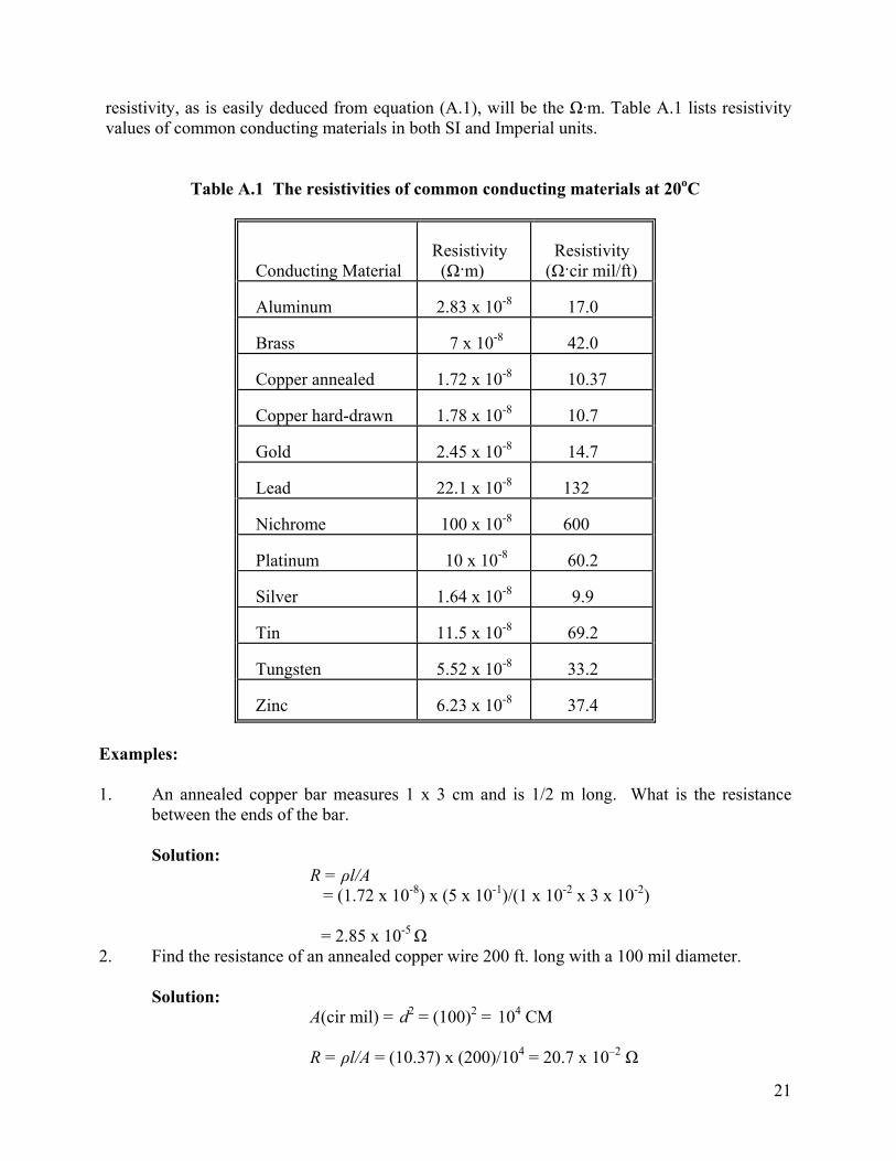

22
Temperature Effects
For most conductors as the temperature increases either from current flowing through it or by heat absorption from the surrounding medium the resistance increases This is due to the increased molecular movement within the conductor which hinders the flow of charge The resistance increases almost linearly with increase in temperature
The relationship between temperature and resistance is expressed as (|T| + t1)R1 = (|T| +t2)R2 (A5) where |T| is the inferred absolute zero of the material involved in oC R1 is the resistance of the material at the temperature t1
oC R2 is the resistance of the material at the temperature t2
oC
The relationship between temperature and resistance may be expressed by
R2 = R1 [1 + α1(t2 - t1)] (A6) where α1 is the temperature coefficient of resistance
R1 is the resistance at the temperature t1 and
R2 is the resistance at the temperature t2
Table A2 lists the inferred absolute zero and temperature coefficients of common conducting materials
Most materials exhibit an increase in resistance with an increase of temperature and are said to have a positive temperature coefficient of resistance However some materials such as carbon and semiconductor materials exhibit a decrease in resistance with an increase of temperature and are said to have a negative temperature coefficient of resistance Examples 1 What is the resistance of an annealed copper wire at 10oC if the resistance is 50 Ω at
60oC
Solution (|T| + t1)R1 = (|T| +t2)R2 t2 = 60o R2 = 50 Ω |T| = 2345o
t1 = 10oC R1 =
R1 = (|T| + t1) R2 (|T| + t2)
= 50 x (2445)(2945) = 415 Ω
23
2 What is the resistance of a copper wire at 10oC if the resistance at 20oC is 433 Ω and if
α1 = 000393
Solution
R2 = R1(1 + α1 ΔT)
= 433 [1 + 000393 (10-20)] = 416 Ω
Table A2 Inferred absolute zero and temperature coefficients for common conducting materials
Conducting
Material
Inferred Absolute zero (C)
Temperature coefficient (Ω CΩ at 0oC)
Aluminum
-236
000424
Brass
-480
000208
Copper annealed
-2345
000427
Copper hard drawn
-242
000413
Gold
-274
000365
Lead
-224
000466
Nichrome
-2270
000044
Platinum
-310
000323
Silver
-243
000412
Tin
-218
000458
Tungsten
-202
000495
Zinc
-250
000400
24
A1 2 Wire Tables [3] Circular cross-section wire is designed by a gauge size of number representing a certain diameter wire The wire table is designed primarily to standardize the size of wire produced by manufacturers The American Wire Gauge (AWG) sizes are given in Table A3 Note that the larger the gauge number the smaller the diameter of the conductor
Table A3 American Wire Gauge (AWG) Sizes of Copper Wire [3]
APPLICATIONS
AWG
AREA (CM)
Ω1000 ft (200 C)
Max Current
(900 C) Power distribution
00
133100
0078
186
1
83690
0124
137
4
41470
0240
89
House main power carriers
6
26240
0395
65
8
16510
0620
48
Lighting outlets general home use
12
6530
1588
20
14
4110
252
15
Television radio
20
10215
101
-
22
6424
161
-
Telephone instruments
28
1598
649
-
35
315
3290
-
40
99
10490
-
An examination of the table shows that if the gauge number changes by 10 the cross-
sectional area changes by approximately a factor of 10 Thus the resistance also changes by approximately 10 times For example AWG 4 has a cross-sectional area of 41470 CM and resistance of 0240 Ω1000 ft whereas AWG 14 has a cross-sectional area of 4110 CM and a resistance of 252 Ω1000 ft ie an increase of 10 in the gauge number represents a decrease in the area by a factor of approximately 10 and an increase in the resistance by a factor of approximately 10 A13 Types of Resistors
Resistors are used for many purposes and are therefore made in many forms The most common of the resistor types are the carbon composition resistor the wirewound resistor the
25
metal film resistor and the carbon film resistor They all belong in either of two groups fixed or variable
The most common of the low-wattage fixed-type resistors is the carbon composition resistor It is made of hot-pressed carbon granules mixed with varying amounts of binding material to achieve a large range of resistance values They are used extensively in electronic applications They are relatively inexpensive reliable and free of stray capacitance and inductance They are available in power ratings up to 2W with resistance values in the range of 1 to 22 MΩ and 5 to 20 tolerance The resistance value of carbon composition resistors and tolerances are specified by a set of colour-coded bands painted on the resistor body Each colour represents a digit in accordance with Figure A1 in the appendix of Exp 1040-EL1 The resistance value as indicated by the colour bands of carbon composition resistors is called the nominal value of resistance Wire wound resistors are commercially available for high precision low resistance and high power dissipation applications They usually consist of Nichrome or copper-nickel wire wound on a ceramic tube and protected from mechanical and environmental hazards by a protective coating of vitreous enamel or silicone Their resistance values range from 1Ω to 100 kΩ with a tolerance range of 00005 and above and a maximum power rating of 200 W
A third group of resistors consist of a thin film of material deposited on insulating materials to provide very high resistance paths Depending on the material used the resistors are classified as carbon film metal film or metal-oxide film resistors Their values range up to 10000 MΩ
Variable resistors come in many forms but basically they can be separated into the linear or non-linear types Variable resistors usually have three leads two fixed and one moveable If contacts are made to only two leads of the resistor the variable resistor is being employed as a rheostat If all three contacts are used in a circuit it is termed as potentiometer or pot The value of the overall resistance and the power ratings of variable resistors are usually stamped on their cases Because the resistance of a conducting film varies with length cross-section and temperature it is possible to use resistance measurement to sense changes in any of those parameters A device that responds to one physical effect is called a transducer Electrical transducers are often used in instrumentation for non-electrical quantities such as temperature light and strain The resistance of the device can be measured and the magnitude of the physical or chemical parameter inferred from the resistance value Typical examples of resistive transducers are 1 The thermistor a two-terminal semiconductor device designed specifically to exhibit a
change in electrical resistance with a change in its body temperature 2 The strain gauge a device which converts linear dimension changes into resistive
changes 3 The photoconductive cell a two-terminal device whose resistance depends upon the
intensity of light impinging on the cell
EXP 1040-EL3 Applications of Resistive Networks PURPOSE To (1) investigate the idea of voltage division using a single source and (2) to examine the utility of a Wheatstone bridge circuit for resistance measurements 10 INTRODUCTION
Using the laws discussed in the course material ndash namely Ohmrsquos law Kirchhoffrsquos Voltage Law (KVL) and Kirchhoffrsquos Current Law (KCL) ndash we are now in a position to study many different circuits having a variety of real-world applications In this lab we consider two such applications and while the analysis associated with them is relatively straight forward they are of significant modern-day importance 11 Voltage Divider Circuits
A voltage source is sometimes required to supply a particular voltage to a load and in fact it may be required to supply several loads with certain specified voltages simultaneously Ideally the voltage supplied should not depend on the size of the load
As a first example consider the circuit shown in Figure EL31 in which a simple voltage
divider circuit is connected in series with the load Notice the situation has been depicted in two equivalent ways In the second schematic the negative terminal of the source is assumed to be electrical ground An electrical ground is a reference level from which other voltages are measured An ideal electrical ground can absorb an unlimited amount of current without changing its potential Here then conventional current flows from the positive terminal of the source through the resistors and back to the source via the ground path (the closed path connection is not explicit in the schematic diagram but it is understood)
Figure EL31 Two equivalent schematics (a) and (b) for a simple voltage divider
From Section E251 of the class notes Electric Circuits Module we know that
⎥⎦
⎤⎢⎣
⎡+
=Ls
LsL RR
Rvv (1)
26
However this type of voltage divider has a serious disadvantage since the value of vL depends on the value of iL and the latter will change depending on the value of the load resistance
To help overcome the problem referred to above it is possible to construct a voltage divider with a bleeder resistor RB as shown below in Figure EL32 and as discussed in Section 251 (page 29) of the class notes Electric Circuits Module
Figure EL32 Two representations (a) and (b) of a voltage divider with a bleeder resistor Strictly the voltage across the parallel section of the circuit is (by the voltage divide lsquorulersquo)
⎥⎦
⎤⎢⎣
⎡+
=)||(
||
BS
LBsL
LRRRRRvv (2)
where
⎥⎦
⎤⎢⎣
⎡+
=LRR
RRRRB
LBLB || (3)
As shown in the class notes the advantage of this kind of voltage division is that when RBltltRL the load voltage is essentially independent of the load resistance and
⎥⎦
⎤⎢⎣
⎡+
=BS
BsL RR
Rvv (4)
Because the load voltage is less affected by the load resistance in this situation we say there is better voltage regulation in this circuit than that in Figure EL31 12 The Wheatstone Bridge The Wheatstone bridge circuit is mainly used to measure an unknown resistance However the principle of the Wheatstone bridge is used in many transducers ndash devices that convert one kind of energy into another ndash and instrumentation systems to measure a physical variable such as 27
strain temperature and pressure A Wheatstone bridge circuit is shown in Figure EL33 In this figure R3 is a variable resistance which models the transducer If a change in physical variable results in a change in resistance of the transducer the Wheatstone bridge can be used to convert the change in resistance to a change in voltage which can be measured
Figure EL33 A Wheatstone bridge
When the voltage vab is zero the bridge is said to be balanced If two resistances (say R1 and R2) are known and another (say Rx) is unknown then a fourth adjustable known resistance R3 (potentiometer) can be used to determine the unknown resistance Rx under balanced conditions When R3 is actually a transducer whose resistance changes with some change in a physical parameter such as temperature then if R1 R2 and Rx are known the voltage vab is an indicator of the size of the measured parameter Balanced Conditions As noted for balanced conditions the voltage vab is zero Also under these conditions using the voltage divide rule twice gives
⎥⎦
⎤⎢⎣
⎡+
=x1
x
RRRvvad (5)
⎥⎦
⎤⎢⎣
⎡+
=32
3
RRRvvbd (6)
We have also seen from Section 254 of the Electric Circuits Module lecture notes that
32
1x R
RRR ⎟⎟
⎠
⎞⎜⎜⎝
⎛= (7)
Unbalanced Conditions When the bridge is not balanced ndash ie vab ne 0 ndash then using Kirchhoffrsquos laws it is straight forward to show that
⎥⎦
⎤⎢⎣
⎡+
minus+
=32
3
x1
x
RRR
RRRvvab (8)
28
29
From this equation we see immediately that if any three of the resistances are fixed in value then a change in the other resistance results in a change in vab Thus a variation in vab is effectively a measure of a change in the variable resistance REFERENCES [1] The Introduction and Appendix A of laboratory exercise EXP 1040-EL1 [2] EW Gill Engineering1040 Mechanisms and Electric Circuits Electric Circuits Module 2008 20 PRELAB 21 Carefully read Section 1 (Introduction) of this experiment and the sections referred to in reference [2] 22 Refer to Figure EL31 The series dropping resistor has a value of 10 kΩ (a) Determine the value of the load resistor RL so that vL = 75 V if the source voltage is 10 V (b) If the load resistance is increased by 25 calculate the new vL 23 Refer to Figure EL32 (a) Design a voltage divider (ie find Rs and RB) for the load
resistance RL obtained in part (a) of Question 22 so that it can operate at vL = 75 V from a 10 V source Assume that the bleeder current iB is 75 mA (b) If the load resistance is increased by 25 calculate the new load voltage Compare this result with that obtained in Question 22 (b) Comment on the comparison
30 APPARATUS AND MATERIALS
1 Fluke 8010A Digital Multimeter (DMM) 1 Sun Equipment Powered Breadboard Model PBB-4060B Standard Resistors 1 kΩ 3 times 120 Ω others as calculated in design Potentiometers 200 Ω 5 k Ω One set of leads with banana plugs and alligator clips and various connecting wires
40 EXPERIMENT 41 Voltage Divider 411 Familiarize yourself with potentiometers ndash the lab attendants will help On the breadboard construct the voltage divider circuit as shown in Figure EL31 using a 1 kΩ resistor for Rs and a 5 k Ω potentiometer (variable resistor) as the load resistor RL Ensure that the source voltage is 10 V after connecting to the circuit Adjust the variable resistor to get an output (load) voltage of vL = 75 V Measure the value of RL for this condition Comment on any discrepancies between the measured and calculated value in Question (22) of the Prelab
30
412 Vary the potentiometer resistance from 680 Ω to 5 k Ω and obtain the load voltage vL in each case Tabulate your results and plot vL as a function of RL 413 Construct the voltage divider found in Figure EL32 and measure the load voltages to
verify your design of Question 23 of the Prelab Use the nearest available resistance values to those you calculated in the design Comment on your findings
42 Wheatstone Bridge 421 On the breadboard construct the Wheatstone bridge circuit of Figure EL33 using three
120 Ω (nominal) resistors for R1 R2 and Rx and a 200 Ω potentiometer (pot) for R3 Also measure and record the actual values of the 120 Ω resistors Ensure that the source voltage v is 10 V after it is connected to the circuit Use the DMM as a voltmeter in the branch between nodes a and b
422 Adjust the pot until the bridge is balanced Measure and record the value of R3 for this
condition Confirm your observation by calculating R3 from equation (7) and comment on any discrepancies
50 DISCUSSION 51 Comment on probable applications of a voltage divider circuit 52 Discuss any technical difficulties encountered during the lab
_____________________________________________________________________________ EXP 1040-DL1 Introduction to Logic Gates and Ladder Diagrams PURPOSE To (i) familiarize the student with the basic logic gates AND OR NOT and NAND (ii) implement basic logic gates using relay logic and (iii) learn how to represent logic circuits by means of ladder diagrams 10 INTRODUCTION Logic circuits may be implemented (constructed) in a variety of ways perhaps most commonly today via electronic components In this lab and the next however we consider the implementation of basic logic expressions using a simple circuit board in conjunction with a few pneumatic cylinders This allows us to explore basic logic circuits without having to resort to sophisticated solid state circuitry (transistors etc) 20 PRELAB There is no prelab for this session However students need to read Section D13 pages 10-18 of the Digital Logic Module before the lab session 30 APPARATUS AND MATERIALS 1 Logic Board Various banana plug connectors AC power (from main lab supply) 40 EXPERIMENT
41 Board Familiarization 411 Normally-open Switch To gain familiarity with the laboratory test panel implement the simple circuit shown in Figure DL11 PB1 refers to one of the two push buttons available on the panel This specific circuit utilizes a ldquonormally openrdquo contact When PB1 is pressed the green indicator light should illuminate
31
CGreenPB1
24V N
Figure DL11 Simple circuit employing push button and a green indicator light
412 Normally-closed Switch Repeat exercise 411 using the ldquonormally closedrdquo contact of PB1 See Figure DL12
CGreen
24V N
PB1
Figure DL12 Simple circuit employing a normally closed contact
42 AND Gate
Using the two push buttons PB1 and PB2 implement an AND operation In other words the green indicator light should only illuminate if and only if both buttons are pressed simultaneously In your lab report provide
bull the ladder diagram implementation (similar to Figure DL11 or DL12) bull the standard symbol for a two input AND gate bull The truth table Note that the truth table should include all four combinations
of the two inputs Assume that a high or logic ldquo1rdquo occurs when the button is pressed
bull Provide a practical application of this circuit (hint think safety)
32
43 OR Gate
Repeat part 42 above in its entirety however this time implement an OR operation using the two push buttons PB1 and PB2 In this case the green indicator should illuminate if at least one of the two buttons is pressed For the practical application consider convenience instead of safety
44 OR Gate
Repeat part 42 above for a ldquoNANDrdquo gate Note that this will require normally closed contacts It is not necessary to provide a practical application for this circuit
45 NOR Gate
Repeat part 42 above for a NOR gate Note that this will require normally closed contacts It is not necessary to provide a practical application for this circuit
46 Inequality Comparator Figure DL13 represents a circuit that is sometimes referred to as an inequality comparator Implement the circuit and experimentally determine the truth table Note that this circuit employs both the ldquonormally openedrdquo and ldquonormally closedrdquo contacts of both push buttons In the lab report provide both the common name for this circuit as well as the standard logic symbol Why is this circuit referred to as an ldquoinequality comparatorrdquo
CGreen
24V N
PB1 PB2
PB_2PB_1
Figure DL13 Circuit that implements an ldquoinequality comparatorrdquo
47 Inverter
An inverter or NOT gate can be implemented with a relay as shown in Figure DL14 When the push button is pressed the coil of relay 1 is energized This opens the normally closed contact of relay 1 which turns the Green indicator light off Implement the circuit and experimentally determine the operation In the lab report provide the standard logic symbol for a NOT gate
33
CR1
24V N
PB2
R_1C
Green
Figure DL14 Circuit that implements a NOT gate
48 Latch (Priority on Set)
A relay can also be used to ldquolatchrdquo the state of the output such that the indicator light is illuminated when the push button is pressed and stays illuminated even if the button is released A second push button must be used to reset the circuit back to its initial (ldquoOFFrdquo) state In Figure DL15 PB1 energizes relay 1 when it is pressed One of the sets of contacts on relay 1 is used to maintain the relay energized even if PB1 is released The normally closed contact of button PB2 de-energizes the relay when the button is pressed (ie resets the latch) Implement the circuit and experimentally determine the operation Be sure and verify what happens when both buttons are pressed simultaneously Note that you must use a different set of relay contacts to energize the green indicator light This particular latching configuration is referred to as priority on SET
CR1
24V N
PB1
PB2
CGreen
R_1
R__1
Figure DL15 Implementation of a ldquolatchrdquo circuit using a relay
34
49 Latch (Priority on Re-Set)
An alternative latch configuration is implemented in Figure DL16 This configuration is referred to as priority on RESET Implement the circuit and experimentally determine the operation Be sure and verify what happens when both buttons are pressed simultaneously In terms of operation what is the main difference between ldquopriority on SETrdquo and ldquopriority on RESETrdquo Provide a practical application of both latch configurations (once again think safety)
CR1
24V N
PB1 PB2
CGreen
R_1
R__1
Figure DL16 Implementation of ldquopriority on RESETrdquo
35
_____________________________________________________________________________ EXP 1040-DL1 Introduction to Sequential Circuits Ladder Diagrams and Relay Logic PURPOSE To (i) introduce ladder diagrams and relay logic and (ii) demonstrate a simple pneumatic system 10 INTRODUCTION Ladder Diagrams (Figure DL21) are a graphical representation of sequential control circuits that are widely used in industry Although originally intended as a way of representing relay logic ladder diagrams are now the standard means of programming microprocessor based PLCs (Programmable Logic Controllers) They are prevalent in a many engineering fields including automation process control and manufacturing In this lab a sequential logic circuit will be implemented using the pneumatic test board The pneumatic test board has three pneumatic cylinders that are activated by solenoid valves The position of each cylinder is monitored by two limit switches One limit switch is activated when the cylinder is fully extended and the other is activated when the cylinder is fully retracted By energizing a solenoid you are able to extend a cylinder and by de-energizing the solenoid the cylinder will retract 20 PRELAB There is no prelab for this session However students need to read Unit D2 of the Digital Logic Module before the lab session 30 APPARATUS AND MATERIALS 1 Logic Board Various banana plug connectors AC power (from main lab supply) Compressed air source 40 EXPERIMENT
41 Limit Switch Familiarization
36
Limit switches A0 and A1 in Figure DL21 are used to sense when cylinder A is retracted and extended respectively Each switch incorporates both a normally opened and normally closed set of contacts Cylinders B and C employ switched B0 B1 and C0C1 respectively These six switches are identified on the wiring panel as S1 through S6 An indicator light can be used to verify the operation of the switches Sketch a circuit that illuminates the green light when cylinder A extends and the red light when cylinder A retracts Implement the circuit on the pneumatic test board and verify the operation by manually depressing the limit switches Use the circuit to determine the correspondence between the six limit switches and the wiring terminals S1 through S6
Figure DL21 Ladder diagram (left) for controlling two pneumatic cylinders 42 Solenoid Valve Familiarization
Solenoid valves S1 S2 and S3 control the three cylinders A B and C As shown in Figure DL21 when the solenoid valves are not energized the cylinders are retracted ie pressure is applied to the rod side of the cylinder Energizing the solenoid changes the position of the valve such that the cap side of the cylinder is pressurized and the
37
38
cylinder extends Sketch a circuit that extends cylinder A when push button PB1 is depressed and retracts A when the button is released Implement the circuit on the pneumatic test board and verify the operation There are a many ldquopinchrdquo points on the test board so be sure and keep your fingers away from the cylinders
43 Implementation of a Simple Latch
Using relay 1 design a circuit that latches the state of push button PB1 such that cylinder A extends when PB1 is depressed and stays extended even if PB1 is released The cylinder retracts only when push button PB2 is depressed Implement the circuit on the pneumatic test board and verify the operation
44 Sequential Logic Circuit 1 441 Familiarization with the Logic Sequence
The ladder diagram shown in Figure DL21 is a sequential logic circuit that will make two cylinders follow the sequence Cylinder A ndash extend -gt Cylinder B ndash extend -gt Cylinder A ndash retract -gt Cylinder B ndash retract The operation of the logic circuit can be described as follows
bull Push button PB1 initiates the start of the sequence ie extend cylinder A by activating solenoid A Relay 2 is latched when PB1 is depressed if and only if the last step in the sequence (limit switch B0 retract B) has been completed This also maintains solenoid A energized bull Once cylinder A has finished extending (ie switch A1 is active) the circuit advances to the second ldquorungrdquo of the ladder which activates solenoid B (cylinder B extends) bull When switch B1 is activated (ie B extended) the circuit advances to the third rung in the ladder Relay 4 is latched which in turn resets relay 2 de-energizing Solenoid A and retracting A bull In a similar fashion the fourth rung in the ladder resets relay 3 which retracts B bull Notice that each rung in the ladder is latched by the completion of the action associated with the previous rung
442 Implementation of the Logic Sequence
Implement the circuit described in 441 and verify the operation
45 Sequential Logic Circuit 2
Modify the circuit in section 44 to implement the following sequence
39
Cylinder A ndash extend -gt Cylinder B ndash extend -gt Cylinder B ndash retract -gt Cylinder A ndash retract
5 Lab Report 51 Provide a short written lab report that includes ladder diagrams of all the circuits design during the lab
52 Explain the operation of the circuit developed in part 45 above
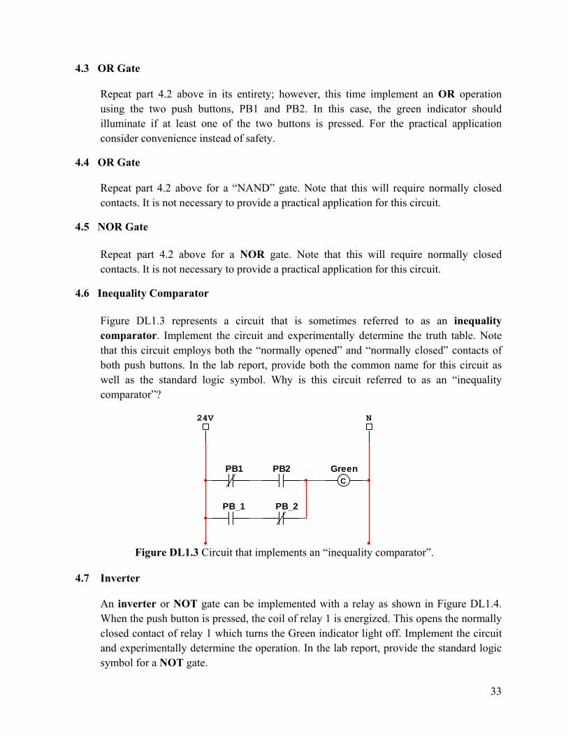
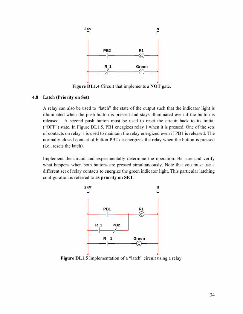
CR1
24V N
PB2
R_1C
Green
Figure DL14 Circuit that implements a NOT gate
48 Latch (Priority on Set)
A relay can also be used to ldquolatchrdquo the state of the output such that the indicator light is illuminated when the push button is pressed and stays illuminated even if the button is released A second push button must be used to reset the circuit back to its initial (ldquoOFFrdquo) state In Figure DL15 PB1 energizes relay 1 when it is pressed One of the sets of contacts on relay 1 is used to maintain the relay energized even if PB1 is released The normally closed contact of button PB2 de-energizes the relay when the button is pressed (ie resets the latch) Implement the circuit and experimentally determine the operation Be sure and verify what happens when both buttons are pressed simultaneously Note that you must use a different set of relay contacts to energize the green indicator light This particular latching configuration is referred to as priority on SET
CR1
24V N
PB1
PB2
CGreen
R_1
R__1
Figure DL15 Implementation of a ldquolatchrdquo circuit using a relay
34
49 Latch (Priority on Re-Set)
An alternative latch configuration is implemented in Figure DL16 This configuration is referred to as priority on RESET Implement the circuit and experimentally determine the operation Be sure and verify what happens when both buttons are pressed simultaneously In terms of operation what is the main difference between ldquopriority on SETrdquo and ldquopriority on RESETrdquo Provide a practical application of both latch configurations (once again think safety)
CR1
24V N
PB1 PB2
CGreen
R_1
R__1
Figure DL16 Implementation of ldquopriority on RESETrdquo
35
_____________________________________________________________________________ EXP 1040-DL1 Introduction to Sequential Circuits Ladder Diagrams and Relay Logic PURPOSE To (i) introduce ladder diagrams and relay logic and (ii) demonstrate a simple pneumatic system 10 INTRODUCTION Ladder Diagrams (Figure DL21) are a graphical representation of sequential control circuits that are widely used in industry Although originally intended as a way of representing relay logic ladder diagrams are now the standard means of programming microprocessor based PLCs (Programmable Logic Controllers) They are prevalent in a many engineering fields including automation process control and manufacturing In this lab a sequential logic circuit will be implemented using the pneumatic test board The pneumatic test board has three pneumatic cylinders that are activated by solenoid valves The position of each cylinder is monitored by two limit switches One limit switch is activated when the cylinder is fully extended and the other is activated when the cylinder is fully retracted By energizing a solenoid you are able to extend a cylinder and by de-energizing the solenoid the cylinder will retract 20 PRELAB There is no prelab for this session However students need to read Unit D2 of the Digital Logic Module before the lab session 30 APPARATUS AND MATERIALS 1 Logic Board Various banana plug connectors AC power (from main lab supply) Compressed air source 40 EXPERIMENT
41 Limit Switch Familiarization
36
Limit switches A0 and A1 in Figure DL21 are used to sense when cylinder A is retracted and extended respectively Each switch incorporates both a normally opened and normally closed set of contacts Cylinders B and C employ switched B0 B1 and C0C1 respectively These six switches are identified on the wiring panel as S1 through S6 An indicator light can be used to verify the operation of the switches Sketch a circuit that illuminates the green light when cylinder A extends and the red light when cylinder A retracts Implement the circuit on the pneumatic test board and verify the operation by manually depressing the limit switches Use the circuit to determine the correspondence between the six limit switches and the wiring terminals S1 through S6
Figure DL21 Ladder diagram (left) for controlling two pneumatic cylinders 42 Solenoid Valve Familiarization
Solenoid valves S1 S2 and S3 control the three cylinders A B and C As shown in Figure DL21 when the solenoid valves are not energized the cylinders are retracted ie pressure is applied to the rod side of the cylinder Energizing the solenoid changes the position of the valve such that the cap side of the cylinder is pressurized and the
37
38
cylinder extends Sketch a circuit that extends cylinder A when push button PB1 is depressed and retracts A when the button is released Implement the circuit on the pneumatic test board and verify the operation There are a many ldquopinchrdquo points on the test board so be sure and keep your fingers away from the cylinders
43 Implementation of a Simple Latch
Using relay 1 design a circuit that latches the state of push button PB1 such that cylinder A extends when PB1 is depressed and stays extended even if PB1 is released The cylinder retracts only when push button PB2 is depressed Implement the circuit on the pneumatic test board and verify the operation
44 Sequential Logic Circuit 1 441 Familiarization with the Logic Sequence
The ladder diagram shown in Figure DL21 is a sequential logic circuit that will make two cylinders follow the sequence Cylinder A ndash extend -gt Cylinder B ndash extend -gt Cylinder A ndash retract -gt Cylinder B ndash retract The operation of the logic circuit can be described as follows
bull Push button PB1 initiates the start of the sequence ie extend cylinder A by activating solenoid A Relay 2 is latched when PB1 is depressed if and only if the last step in the sequence (limit switch B0 retract B) has been completed This also maintains solenoid A energized bull Once cylinder A has finished extending (ie switch A1 is active) the circuit advances to the second ldquorungrdquo of the ladder which activates solenoid B (cylinder B extends) bull When switch B1 is activated (ie B extended) the circuit advances to the third rung in the ladder Relay 4 is latched which in turn resets relay 2 de-energizing Solenoid A and retracting A bull In a similar fashion the fourth rung in the ladder resets relay 3 which retracts B bull Notice that each rung in the ladder is latched by the completion of the action associated with the previous rung
442 Implementation of the Logic Sequence
Implement the circuit described in 441 and verify the operation
45 Sequential Logic Circuit 2
Modify the circuit in section 44 to implement the following sequence
39
Cylinder A ndash extend -gt Cylinder B ndash extend -gt Cylinder B ndash retract -gt Cylinder A ndash retract
5 Lab Report 51 Provide a short written lab report that includes ladder diagrams of all the circuits design during the lab
52 Explain the operation of the circuit developed in part 45 above
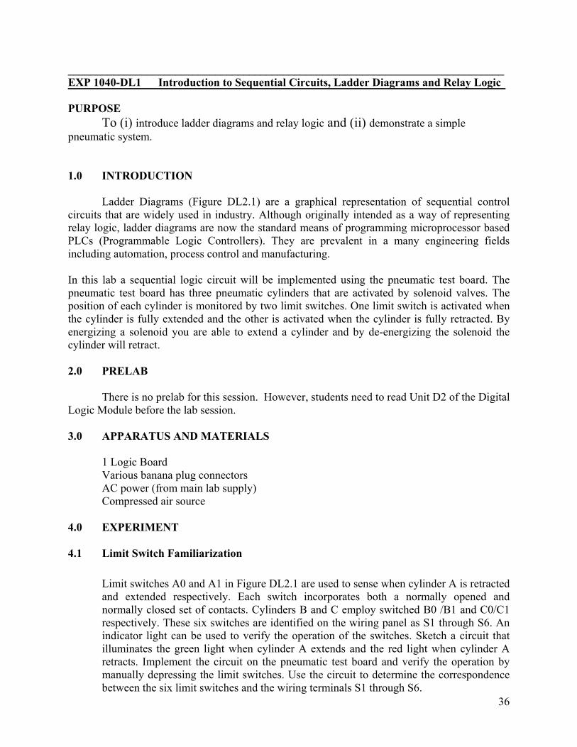