Embed Size (px)
Citation preview


results of one of theThe purpose of this report is to present the
research and development programs which was initiated by the members of
the Ship Production Committee of The Society of Naval Architects and Marine
Engineers and financed largely by government funds through a cost sharing con-
tract between the U.S. Maritime Administration and Bethlehem Steel Corp-
oration. The effort of this project was directed to the development of im-
proved methods and hardware applicable to shipyard welding in the U.S. ship-
yards.
Mr. W. C. Brayton,
Manager, Mr. G. E. Iayer,
Bethlehem Steel Corporation was the Program
Celesco Industries Inc. directed the development
work at the San Diego, California plant. Grateful acknowledgement is made
for the outstanding contribution of Messrs. J. Thommes, H. White, axial G.
Silke of the Celesco organization.
Special acknowledgement is made to the members of Welding Panel
SP-7 of the SNAME Ship Production Committee who served as technical
advisors in the preparation of inquiries and evaluation of sub-contract
proposals.

Report Documentation Page Form ApprovedOMB No. 0704-0188
Public reporting burden for the collection of information is estimated to average 1 hour per response, including the time for reviewing instructions, searching existing data sources, gathering andmaintaining the data needed, and completing and reviewing the collection of information. Send comments regarding this burden estimate or any other aspect of this collection of information,including suggestions for reducing this burden, to Washington Headquarters Services, Directorate for Information Operations and Reports, 1215 Jefferson Davis Highway, Suite 1204, ArlingtonVA 22202-4302. Respondents should be aware that notwithstanding any other provision of law, no person shall be subject to a penalty for failing to comply with a collection of information if itdoes not display a currently valid OMB control number.
1. REPORT DATE MAR 1975
2. REPORT TYPE N/A
3. DATES COVERED -
4. TITLE AND SUBTITLE Development of a Portable AC/DC Welding Power Supply Module
5a. CONTRACT NUMBER
5b. GRANT NUMBER
5c. PROGRAM ELEMENT NUMBER
6. AUTHOR(S) 5d. PROJECT NUMBER
5e. TASK NUMBER
5f. WORK UNIT NUMBER
7. PERFORMING ORGANIZATION NAME(S) AND ADDRESS(ES) Naval Surface Warfare Center CD Code 2230-Design Integration TowerBldg 192, Room 128 9500 MacArthur Blvd Bethesda, MD 20817-5000
8. PERFORMING ORGANIZATIONREPORT NUMBER
9. SPONSORING/MONITORING AGENCY NAME(S) AND ADDRESS(ES) 10. SPONSOR/MONITOR’S ACRONYM(S)
11. SPONSOR/MONITOR’S REPORT NUMBER(S)
12. DISTRIBUTION/AVAILABILITY STATEMENT Approved for public release, distribution unlimited
13. SUPPLEMENTARY NOTES
14. ABSTRACT
15. SUBJECT TERMS
16. SECURITY CLASSIFICATION OF: 17. LIMITATION OF ABSTRACT
SAR
18. NUMBEROF PAGES
90
19a. NAME OFRESPONSIBLE PERSON
a. REPORT unclassified
b. ABSTRACT unclassified
c. THIS PAGE unclassified
Standard Form 298 (Rev. 8-98) Prescribed by ANSI Std Z39-18

P r e f a c e
I11
R e p o r t
I
II
III
IV
REPORT ORGANIZATION
A b s t r a c tExecut ive SummaryA) Prog ram Hi s to ryB) Conclusions Recommendations
O b j e c t i v e s ( S t a t e m e n t o f W o r k ) A) GoalsB) P l a nBasic ConceptA) BackgroundB) Block DiagramC) Design Considera t ions - Elec t r ica l
1) Input Rectifier2) Switch Circuit3) T r a n s f o r m e r4) Output Rectifier5) Control Circuit
D) Design Considerations - Mechanical1) Size and Weight2) Hea t3) Packaging
E) Prob l em Areas1) Switch Circuit2) Component ratings and availabili ty
Areas of InvestigationA) Semiconductor Switch BackgroundB) The Transis tor Switch
1) Types2) Tes t Resul ts
c ) SCR’s1) T y p e s2) Tes t Resul ts
D) Comparison of SCR’s Vs.E) Control Circuitry DesignF ) Trans fo rmer Des ignG) Mechanical PackagingH) Evalua t ion
Finalizing the Candidate DesignA) Fur ther Development
T r a n s i s t o r s
(T rans i s t o r s )
B) Elect ronic Circui t DiagramsC) Theory of Operation

IV Finalizing the Candidate Design (Transistors) (Cent’ d.)c ) Theory of OperationD) Design CalculationsE) Mechanical Design
1) Heat2) Packaging3) Weight
F) Final Performance Test Results
v ConclusionA ) Evaluation of Final Package - Results
1) Welding2) Electronic
B) Recommendations for Future Study

ABSTRACT
This report deals with lightweight power conversion for application and port-ability in the welding industry. It is a final report on a research contract andit includes all the circuits investigated and their potentials. The report alsoincludes a detail description of the final lightweight circuit used. The supplyhas a maximum output of 250 amps at 30 volts and either voltage or currentcould be regulated by a feedback control system. Ninety percent variabili tyis possible with 85 percent efficiency at full load. The unit weighs 98 poundsand is convection cooled only. Input power is 440 VAC 60 HZ 3 0 .

A) EXECUTIVE SUMMARY PROGRAM HISTORY
J a n u a r y1973
System approach under investigation used transistorswitches in bridge configuration. Welding wasaccomplished with this system; however, problemswere encountered with transistor breakdown andoverheating of switches. Failure of input rectifierswas a lso exper ienced. All waveforms displayedlarge amounts of noise. Efficiency was calculatedat 65%.
February 1-15 A number of failures of both switches and rectifiers1973 were encountered . Input bridge rectifier types were
changed to 1N2287. A new transformer was woundwith an increased number of turns in the secondaryto provide a higher voltage under load.
February 16-28 Preliminary investigation was begun on an SCR switching1973 c i r c u i t . Also, parallel tuned LC circuits were inserted
in the primary side of the t rars is tor swi tch t ransformerto correct the switching waveform and reduce harmonics.
M a r c h A short to the core of the power transformer caused1973 destruction of the core. At this time, a smaller core
was obtained and the winding configuration recalculated.The SCR swithes were run at low voltage using capacitorcommuta t ion . Problems were encountered with lock-up.
Apr i l1973
A series switch configuration was suggested to reducethe voltage drop on each transistor. This circuit wasbreadboarded and ies ts s ta r ted . The SCR evaluat ionwas de fe r r ed .
Work was continued on the serial transistor switchapproach. P rob l ems were found in turning off both seriest rans is tors a t exact ly the Same t ime. Minor d i f ferencescaused full voltage to appear across one unit , resultingin its destruction. Transistor type used was RCA 2N6251.Increased t rans is tor dr ive wi th c i rcui ts to remove s toredbase charge more rapidly on rum off failed to make thissys tem opera t ional . DC biasing of the transistor operatingat a higher level was not feasible due to the large amountof power dissipated in the bias circuit.
Delco engineers suggested DTS 804 for this application.Circuit was rebuilt using this single transistor in placeof the series pair.
A parallel investigation was begun on using SCR switches.
May1973
June1973
July1973
August1973
S e p t e m b e r1973
October1973
The transistor switch configuration was operated atefficiencies in excess of 88%; however, voltage andcurrent t rans ients s t i l l caused swi tch des t ruc t ion . Atthis time, it was decided that the remainder of the monthwould be devoted to the SCR intestigation. A switchcommutated system was arrived at which shows considerablepromise in this application. Spec sheets were received on anew Motorola Beam-fired SCR with ratings well in excessof the requirements. Samples were requested .
The transistor switch in bridge configuration was selectedas the best means of achieving success within budget andschedule . Concentrated effort was applied to this circuit ,using DTS 804's. AS a result of careful t iming and wave-shaping, switch dissipation was reduced to a minimum.The system was run for five hours at 100 amperes outputwithout significant heating of the bridge. Input voltage wasincreased incrementally, with waveform observation andcorrection being made at each level. The circuit was oper-ated at full input voltage. Load transient protection andcurrent l imiting circuitry were incorporated in preparationfor tests with an arc.
Saturable reactor current l imi ters were developed forcurrent t rans ient l imi ta t ion . The reactors made a considerable weight contribution of about 20 pounds; howeverthey were very successful at l imiting current transients.As a result the output current could be increased to 250amp at full voltage without destruction of the semiconductors.
The complete breadboard was tested under welding conditionsat full voltage and current; however, at this higher powerlevel, excessive heating was observed.
The breadboard was folded into a mechanical package andtested under welding conditions (SMAW). Problems atrapid turn-on of this input l ine caused destruction of semi-conductor swi tches .
A Zero crossover SCR switch was incorporated into theinput rectifier to reduce the secondary peaks encounteredin rapid turn-on. Modera te success was achieved.
Additional bypass capacitors were added to reduce furtherswitch heating and voltage transients.

November AC welding was achieved with limited success due to the1973 high f requency of t ransformat ion . vol tage process was
added to the unit. Mig welding was successfully per-fo rmed .
December 12 Successful demonstration to Marad Commission and1973 visitors in Bethlehem Steel Sparrows Point Shipyard.
B) CONCLUSIONS
From a welding point of view, the final unit fulfilled asubstantial portion of the desired objectives.
From an economic and reliability point of view, thetransistor design is not optimum. It is felt SCR’s area better device for this application, providing they canbe controlled.
Recommendations for future study:
1) Investigate the use of 220V instead of 440V.
2) In the light of techniques used in this project, re-investigate the use of SCR’s.
3) Investigate the conversion of inversion frequencyback to 60 Hz for AC welding.
4) Investigate a 120V single phase mini supply.
VI

I Objectives
A) Goals
The following is a statement of the desired performance of a light-weight power supply for welding applications.
The basic power supply module shall be capable of supplying a min-mum of 250 amperes of welding current suitable for AC shieldedmetal arc welding within that power requirement.
The basic module shall be adaptable to provide a minimum DC weldingcurrent of 250 amperes of parallel connected with other modules toprovide up to 1000 amperes DC for shielded metal arc and submergedarc welding.
The primary module or combinations of the primary module shall bedesigned to support shipyard production welding. Production weldingincludes the following types of operation:
1.
2 .
3.
4 .
5.
6.
7 .
8.
9 .
10.
Automatic submerged arc welding of plate butts in downhandpos i t ion .
Semi-automatic sub-arc and/or MIG welding of butt weld and largefillets which are not accessible to machine driven equipment.
Manual stick electrode welding using large diameter electrodesfor downhand fillets and short butts. Gravity welding is also inth is ca tegory .
Elec t ro-s lag and/or e lec t ro-gas welding of ver t ica l but t sand bulkheads.
Consumable nozzle welding of
All position MIG welding with
vertical butts in stiffeners
smal l d iameter e lec t rode .
in shell
and g i rder
All position stick electrode welding.
Small amounts of special steel and non-ferrous welding both MIGand manual.
Arc gouging second sides of butt welds and correcting defective weld
P l a s m a - a r c o p e r a t i o n s .
Pr imary and in t ra-modular commotions shall be of a plug-in type wherepractical so as to mini mize the use of a skilled technician for maintenan
Pr imary power sou re r shall be 440-480 volt three phase 60 cycle AC.Consideration may be given to higher irequency or other power sourcec h a r a c t e r i s t i c s .

A) Goals (Continued)
The basic module shall be capable of compensating for fluctuationsin primary line voltage Up to plus or minus 10% with no primary power limitation. Welding power shall remain constant within plusor minus 1%. Use of a closed loop system is desired in function.
Visual and/or audible signals shall be provided to indicate majorpower Supply module sub-system failure.
Each module or paralleled group of modules shall be capable of beingcontrolled from the operator location. Each module shall be capableof automatic operation through the foot pedal control system.
Each basic module shall be rectangularly shaped to allow easystacking during use and storage.
The design goal for the weight of a basic module is 40 lbs. A basicmodule includes no cables, brackets or attachments. Shipyard move-ment without the use of cranes and riggers is highly desirable.
Cooling shall be by convection and conduction.
The ambient temperature operating range of the basic module s h a l lbe from 0° to 120° F.
Duty cycle shall be 100%.
Maintainabili ty:
The basic module shall not be open to the ambient environment. Themodule shall be free from vents and openings.
T h e b a s i c m o d u l e w i l l n o t b e w a t e r c o o l e d .
The basic module shall not be cooled by ducted or forced air.
Power supply sub-sys tem components shall be plug-in modules wherep r a c t i c a l .
Construction of the module shall be in accordance with good commercialp r a c t i c e . The module shall be capable of withstanding reasonablyrough handling and transportation environments.
Design of the module shall provide easy access to the interior of thecase to allow repair and replacement.
M a t e r i a l s :
The module shal l conta in suppl ies , products , or mater ia ls manufacturedwithin the U. S. A.
2

B) P l a n
The basic approach taken with this reacarch project is ratherr e v o l u t i o n a r y . It is obvious that welding power supply operatingfrom the 440 VAC 60 Hz line can never be made to meet the designgoals d iscussed above , especially in regard to weight, duty cycleand cooling. Instead of using a conventional 60 llz transformer, ahigh frequency lightweight and efficient converter system is used.The basic concept is explained in Section II. For this reason, muchof the research involved in this project is electronic in nature; there-fore, much of the discussion in this report deals with the electronicsof the proposed welding supply.
The method and plan of this research program is outlined in t h efollowing statement of work followed by the Celesco Engineering Staff.
1. Es tabl i sh Design Goals and Prepare Conceptual Elec t r ica l Des ign
a . Es tabl i sh Design Goals
Prepare documentation to guide the design and analyses of thepor table power supply . This document will compile and com-bine des i red por t ions of welding research projec t SP-1-2(203.01) and Celesco proposal 0572-4-5.
b . Conceptua l Des igns
Prepare 2-4 feas ib le e lec t r ica l c i rcui t s wi th b lock d iagramsa n d s c h e m a t i c s . C o n t a c t s e m i - c o n d u c t o r m a n u f a c t r e r s a n ddetermine which s ta te-of- the-ar t components can cont r ibuteto advanced designs. Rev i ew t r ans fo rmer co re manufac tu r e r s ’capabi l i t ies to provide advanced l ightweight t ransformers .
c . Selec t the Most Promis ing Circui t Des igns
(Formal Review)
2. Opt imize Circui t ry and Perform Assembly Tests
a . Opt imize Circui t ry of Selec ted Designs
Analyze each of the promising concepts for theoretical heatcont r ibut ion of the power supply sub-assembl ies . U t i l i z ei n f o r m a t i o n o n s t a t e - o f - t h e - a r t s e m i c o n d u c t o r s a n d c i r c u i t r yto reduce hea t cont r ibut ions . Examine each subassembly forits weight contribution and optimize. This ac t iv i ty concernspr imar i ly e lec t r ica l c i rcui t ry and does not inc lude des ignsof the case, r e c e p t a c l e s , e t c .
b . Sub -Assembly Tes t
S e l e c t p r o m i s i n g c i r c u i t s a n d s u b - a s s e m b l i e s f o r b r e a d b o a r dtype fabr ica t ion and tes t . P r o c u r e s e l e c t e d s u b - a s s e m b l yc o m p o n e n t s , a s s e m b l e a n d t e s t . Determine hea t cont r ibut ionsand abili ty to achieve various target weights.
3

(c) Review and Select Sub-Assembly Concepts Which Test DataSubstantiates as Meeting Rcasonable Requirements
(Formal Review)
3. Fabricate Breadboards and Test
a. Prepare Candidate Circuitry Designs
Prepare circuit designs utilizing data from sub-assembly tests.Calculate thermal and mass properties of selected concepts.Determine control circuitry design and prepare to verify per-formance by incorporation in breadboard testing. Preparebreadboard test drawings of the power supply electrical systemand prepare parts lists.
b. Assemble and Test Breadboard Electrical Systems
Procure and fabricate breadboard parts. Assemble the systemto include sub-systems and test the power supply characteristicsunder a dummy load and while welding.
Provide system information to allow test prototype design.
Reduce power supply breadboard design features to a minimumin order to concentrate on the switching circuit with full linevoltage.
Research adaptation of other industry power supplies and applygood features.
c. Review Results of Breadboard Testing
Review the results of the breadboard activity to arrive at thedesired configuration for further development.
Establish the basic circuitry for the test prototype. Concentrateon the major design goals of power, control and reliability.
Continue the breadboard test and development concurrent withthe evolution of a test prototype.
4. Prepare Prototype Design
a. Utilize Breadboard Test Data to Upgrade the Packaging Concept
Examine the on-going test results and identify proven approaches.
b. Prepare Power Supply Test Prototype Design (Preliminary)
Prepare preliminary power supply design. Provide a conceptfor case and heat sink configuration. Conduct preliminary thermaland mass characteristic analyses.
4

c. Determine Analytical Feasibility of Design Goals
(Formal Review)
5. Fabricate and Test a Test Prototype Power Supply
a. Prepare Final Prototype Design
Prepare final design of the prototype power supply. Providemultiple case designs if necessary. Conduct analyses toinclude design modifications. Prepare a parts list. Procureand fabricate parts. Assemble the test prototype system.
b. Prepare a Prototype Test Plan and Equipment List
c. Conduct Tests
Conduct tests of the prototype to determine its capability.Compare results with the design goals.
Modify the prototypes as required to approach design goalperformance and maintain similarity to concurrent bread-board advancements.
Conduct a short period of controlled shipyard testing in SanDiego. Record results.
Within budget and schedule constraints, the prototype unitwill be tested and modified to approach design goals.
6. Documentation and Final Report
Prepare a final report which describes the chronological eventsof the program.
This report will include unsuccessful approaches, as well assuccessful.
Schematics, drawings, pictures and test results will be included.
II Basic Concept
A) Background
The primary source of weight in any standard power supply isthe iron core transformer. These transformers are designedfor operation at a 60 cycle line frequency. The efficiencies en-countered at these frequencies require a large transformerthat is capable of supplying the necessary power.
In the 1940's new power supplies appeared in use, primarily inmilitary equipment, which were designed for operation on a 400cycle line. As a result of the increased efficiencies thus ob-tained, these supplies were from 1/3 to 1/2 the size of their 60cycle counterparts.
The supply to be developed under this contract was based upona logical extension of this principle. The 60 cycle input powerwas to be rectified and converted to a DC level. This DC voltagewas then to be switched at a much higher frequency. In thefrequency range selected, from 5 to 10 KHz, a small toroidaltransformer using a ferrite core can be used. The overall weightreduction to be realized is in excess of 10 to 1. An equivalentreduction in size is also obtainable.
B) Block Diagram
To achieve the results described, five basic building blocks arerequired. These blocks and their relationships are illustratedin Figure II-A
Figure II-A
B) Basic Concept (Continued)
As shown, the function of the input rectifier is to convert the440V, 60 input to a DC level. This level is a function of theAC input voltage, in this case approximately 650 VDC.
The next circuit, the switch, converts the 650 VDC to asquare wave alternating at 7 KHz at the same voltage level.This higher frequency AC voltage is then applied to the toroidaltransformer where it is reduced to 20 to 40 volts as required,at a maximum of 300 amperes.
The contro l c i rcui t performs three bas ic funct ions . F i rs t , i tcontrols the action of the switches, turning them off and on inthe proper relationship. Its second function is to convert inputsignals from the current control switch and from the foot pedalinto switch control outputs. Its third function is to monitor theoutput current and hold it at the selected level despite variationsin arc length.
The last block, the output rectifier, converts the transformerAC output to a pulsating DC for DC welding. Alternate outputterminals apply the AC output directly from the transformer tothe torch.
c ) Design Considera t ions - Elec t r ica l
1. Input Bridge Rectifier
AC to DC conversion may be accomplished by using a standard3 phase bridge circuit . Diode selection is based upon thevoltage and current operating levels. Three of the six rec-tifiers can be replaced by SCR’s to provide on/off capabilitysimilar to that of an output contactor on conventional weldingm a c h i n e s .
2 . Switch Circuit
This is one of the more critical areas of design. The switchingcomponents must operate at high voltage and current, as wellas having the capability of very rapid switching. In addition,switching transients must be minimized to avoid destructivep e a k s . Switching components must be held in the on and offstates with a minimum of time between. Since most of thepower lost in a switch is lost during the switching interval,excessive switching times result in loss of efficiency andcomponent overheating and possible damage. It can furtherbe seen that switch efficiency improves as an inverse functionof frequency since the switching interval becomes a proportion-ally small percentage of the overall period. Figure II-Billustrates a typical voltage waveform of a semiconductor deviceswitching into a transformer load.

Voltage Waveform
Figure II-B
3. Output Transformer
The Output Transformer effects the energy conversion froma high voltage to a lower one at an increase in current capability.The use of ferrite core material is indicated to provide thenecessary reduction in size and weight.
To provide a voltage output of 20 or 40 volts from the 650V in-put, transformer turns ratios of 32:1 and 16:1 were indicated;thus, a center-tapped primary is required. However, tocompensate for output loading, ratios of approximately one-half the above amount will be used. Open circuit voltages of40V and 80V will be generated, procducing the required levelsunder load. Transformer design calculations are presentedin Section III-C-3.
4. Output Rectifier
The output rectifier section converts the transformer AC toto DC. A full wave rectifier will be used with a shunt in thecommon leg for output current detection. Since the outputvoltage levels are relatively low, the primary considerationis that of the current carrying capacity of the selected deviceand the speed of recovery.
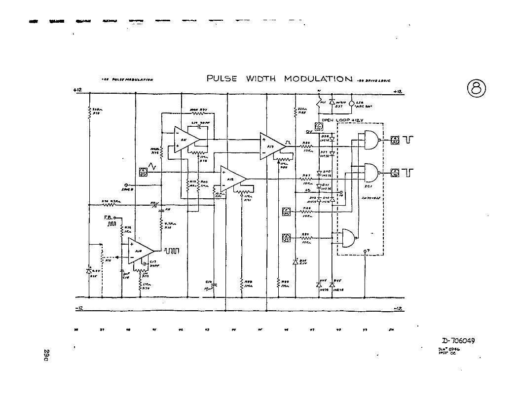
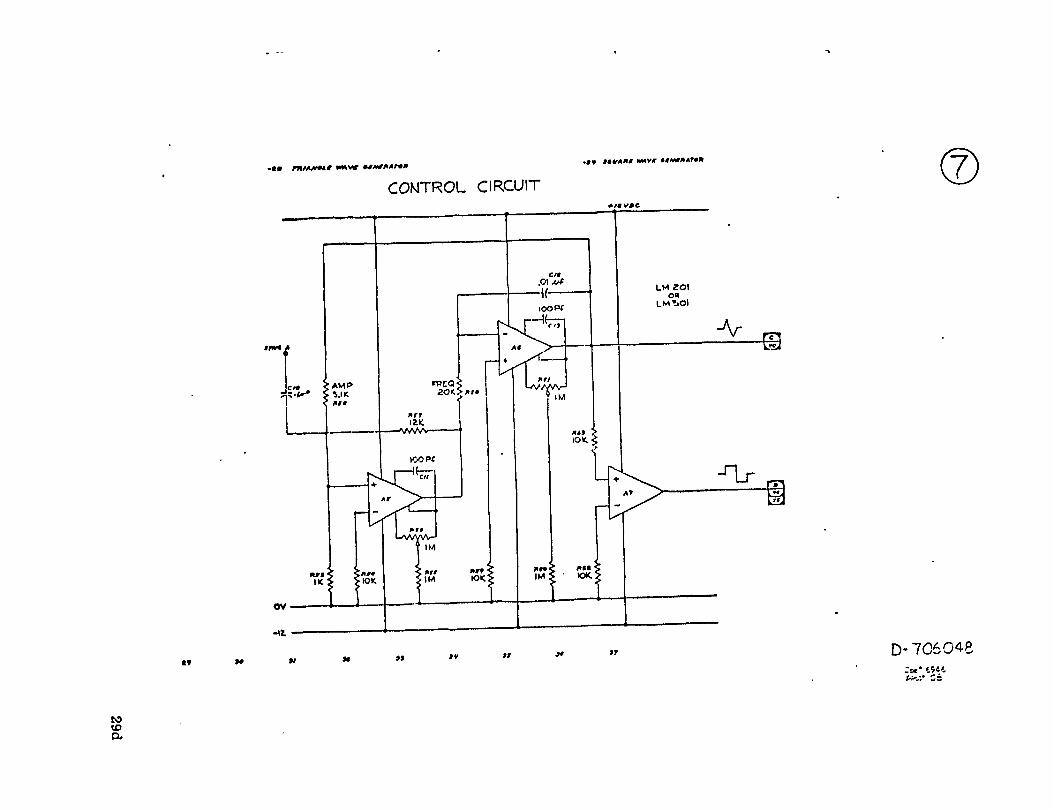
5. Control Circuit
The control circuit must receive a reference signal from eithera foot pedal or a selector on the machine itself. It must alsoreceive a feedback (SMAW or TIG), or a voltage divider for avoltage process (MIG). The control circuit must compare thereference and the feedback signal and then drive the switchesin a nccessary manner to achieve a zero difference or errorsignal.

5. Control Circuit (Continued)
The control circuit in conjunction with the power switcheswill provide variabili ty. By utilizing some sort of pulse widthcontrol, the power to the transformer can be precisely con-t ro l led .
The control circuit must also provide some sort of currentlimiting so as to protect the semiconductors in the switchesf r o m o v e r c u r r e n t .
D) Design Considerations - Mechanical
1. Size and Weight
Keeping size and weight to a minimum are primary objectivesof this program and are the major mechanical considerationsin packaging the unit. Factors which determine size and weightare (1) total size and weight of required components, (2) sizeand weight of heat sinks required for adequate cooling, and(3) packaging concept.
Early in the program it was apparent that component quantityand size would not be the limiting factor as those selected forthe early breadboard would readily fit into the required space.This left size and weight of required heat sinks along withpackaging techniques as the major considerations.
2 . Hea t
A requirement of the system is that all cooling be naturalconvection in order to improve reliabili ty and reduce maint-enance problems associated with fans and blowing unfilteredair over heat sinks and components. At an efficiency of 90%the maximum output expected is 12,000 watts with 1333 wattsto be dissipated. At 80% efficiency the dissipation would be3000 watts. Final efficiency is expected to be bounded by thesetwo limits. Using natural convection cooling, the major problembecomes available surface area on the exterior of the package.Through breadboard evaluations actual heat dissipation can bedetermined which can then be used in making the necessaryheat sink calculations.
3. P a c k a g i n g
Basic considerations for the packaging concept other thanminimum size and weight are simplicity through a ruggedfunctional design. The center of gravity and handles shouldbe suitably located for ease of handling. The unit must bedesigned to withstand the abuse of shipyard environment. Itmust also be water tight in the final design and all exposedcomponents be covered and insulated from the outside. T h eentire case and all heat sinks must be grounded to preventhazard f rom elec t r ica l shock.
9
E) Problem Areas
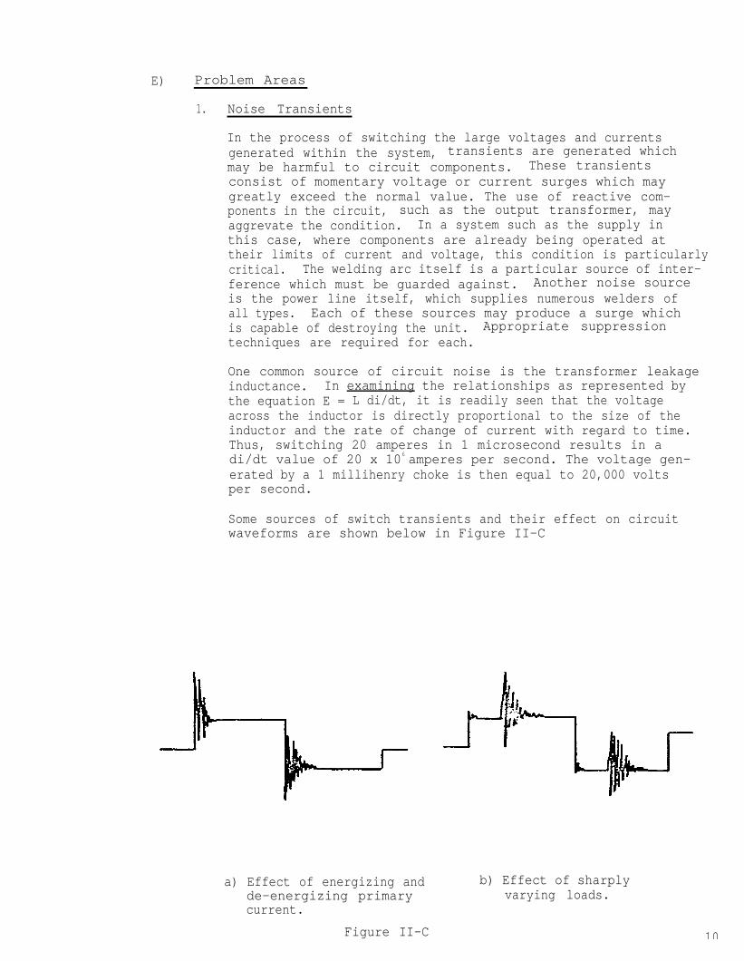
1. Noise Transients
In the process of switching the large voltages and currentsgenerated within the system, transients are generated whichmay be harmful to circuit components. These transientsconsist of momentary voltage or current surges which maygreatly exceed the normal value. The use of reactive com-ponents in the circuit, such as the output transformer, mayaggrevate the condition. In a system such as the supply inthis case, where components are already being operated attheir limits of current and voltage, this condition is particularlycritical. The welding arc itself is a particular source of inter-ference which must be guarded against. Another noise sourceis the power line itself, which supplies numerous welders ofall types. Each of these sources may produce a surge whichis capable of destroying the unit. Appropriate suppressiontechniques are required for each.
One common source of circuit noise is the transformer leakageinductance. In examining the relationships as represented bythe equation E = L di/dt, it is readily seen that the voltageacross the inductor is directly proportional to the size of theinductor and the rate of change of current with regard to time.Thus, switching 20 amperes in 1 microsecond results in adi/dt value of 20 x 106 amperes per second. The voltage gen-erated by a 1 millihenry choke is then equal to 20,000 voltsper second.
Some sources of switch transients and their effect on circuitwaveforms are shown below in Figure II-C
a) Effect of energizing andde-energizing primarycurrent.
Figure II-C
b) Effect of sharplyvarying loads.
10

1. Noise Transients (Continued)
As can be seen from Figure II-C, abrupt changes, typicalof normal circuit operation, may produce levels which arein themselves destructive and in addition which may producea rate of change which exceeds component specifications.
Additional problems are encountered in the responses of thesemiconductors themselves. The stored charge may alsoproduce undesired transients.
Suppression of these transients may involve a number oftechniques. A final design will usually require a number ofthese.
The simplest method is that of the bypass capacitor. Thiscapacitor, placed in parallel with a switching component,acts to absorb the undesired signal. (Figure II-D.)
a) Switching Transient
b) Effect of Bypass Capacitor
c) Overcompensation
Figure II-D
1. Noise Transients (Continued)
The use of bypass capacitors on the input bridge rectifiercompletely eliminated the catastrophic failures previouslyexperienced in this area.
More elaborate filters may be composed of resistors, in-ductors or capacitors in combination. For example, a seriesR-C circuit was found to be required across the gate input ofan SCR. Series inductors, with parallel RC circuits are alsoused to control commutation transients. It should be noted,however, that these circuits may, themselves, introduce un-desired distortions which require further compensation.
Another method of transient control is by means of voltage limiters. The two basic components of this type are zenerdiodes and varistors. Both of these components display thecharacteristic of having no effect upon a circuit until a specifiedvoltage level is exceeded. At this time, the units conduct,absorbing the undesired peak. In the lightweight power supply,varistors are placed across each transistor switch for over-voltage protection. Zener diodes are used in the transistorbase circuits for the same purpose.
2. Component Ratings and Availability
A basic requirement of the switching circuit is the ability to switch up to 30 amperes at 650 volts. Although a number oftransistors were available at the beginning of the programwhich were capable of switching the desired current, nonecould do so at the required voltage. Thus, it became necessaryto parallel a number of transistors of lower rating to meet thecurrent requirement. This problem is aggravated by the factthat the current handling capabilities of transistors must beheavily derated as the operating voltage is increased. Thespecific components selected, and the trade-offs involved, willbe discussed.

III Areas of Investigation
A) Semiconductor Switch Background
As was noted in the previous section on problem areas, the mostsignificant obstacle posed by this project is the switch circuit . T h econversion from 650 VDC to 7000 Hz AC must be accomplished bysemiconductor switches in order to maintain efficient l ightweightconvers ion .
There are two types of semiconductor devices that can be used in alightweight power conversion system; the Silicon Controlled Rectifier(SCR) or the Silicon Transistor. In addition to these two devices,there are numerous configurations in which the two can be operated.The optimum device and configuration must be chosen to minimizeweight and maximize efficiency.
In addition to the problems mentioned in the previous section onnoise and component availabili ty, there is also problems involvedin energy dissipation. Two types of dissipation are:
1. Saturation dissipation - power lost during the onstate of a device. SCR's have an inherently highersaturation voltage than do transistors, and thushave h igher sa tura t ion losses .
2 . Switching dissipation - power lost in the transition fromthe on to off state. Trans is tors have an inherent problemof saturation delay time; this causes higher switchingl o s s e s .
B) Trans is tor Conf igura t ions
The basic inverter configuration used for transistor switching isthe bridge configuration, s ince t rans is tor vol tage ra t ings preventa center - tapped configuration. Therefore, only the switch designis discussed in the following discussion on transistors. Keep inmind, four sets of switches are used even though only one set isd i s c u s s e d .
Se r i a l T rans i s t o r s
Initial investigations into inverter operation used Delco transistortype DTS 721 in parallel banks. The maximum collector rating of800 volts appeared to allow sufficient margin for satisfactory opera-tion at the required 650 volt level. Since the transistor is capableof switching only approximately 3 amperes at this level, it wasnecessary to parallel ten units to provide the desired current capa-bil i ty. However , in attempting to operate at these levels, extensivecomponent damage was realized from reiatively minor overvoltageconditions. Due to this, i t was decided, early in March, to in-vestigate the possibili ty of replacing each single transistor with as e r i e s pa i r . This combination reduces the voltage appearing acrossany one transistor to one-half the former value. Other benef i t s werer e a l i z e d .
13
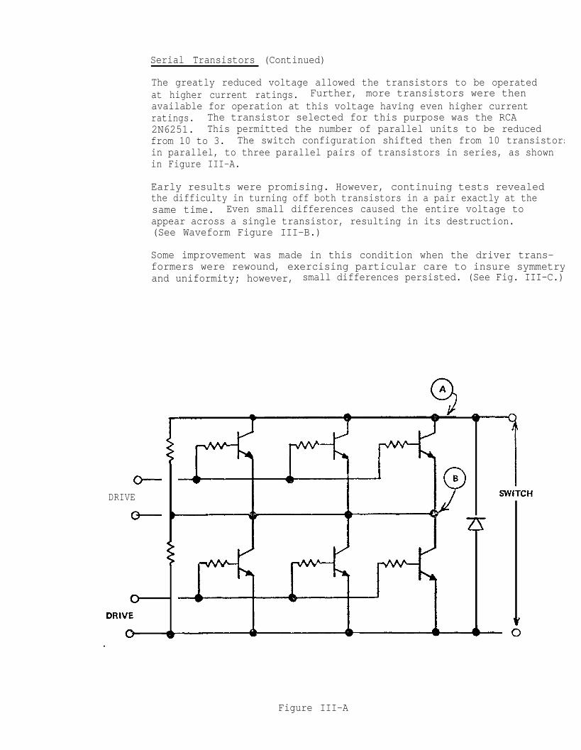
Serial Transistors (Continued)
The greatly reduced voltage allowed the transistors to be operatedat higher current ratings. Further, more transistors were thenavailable for operation at this voltage having even higher currentratings. The transistor selected for this purpose was the RCA2N6251. This permitted the number of parallel units to be reducedfrom 10 to 3. The switch configuration shifted then from 10 transistorsin parallel, to three parallel pairs of transistors in series, as shownin Figure III-A.
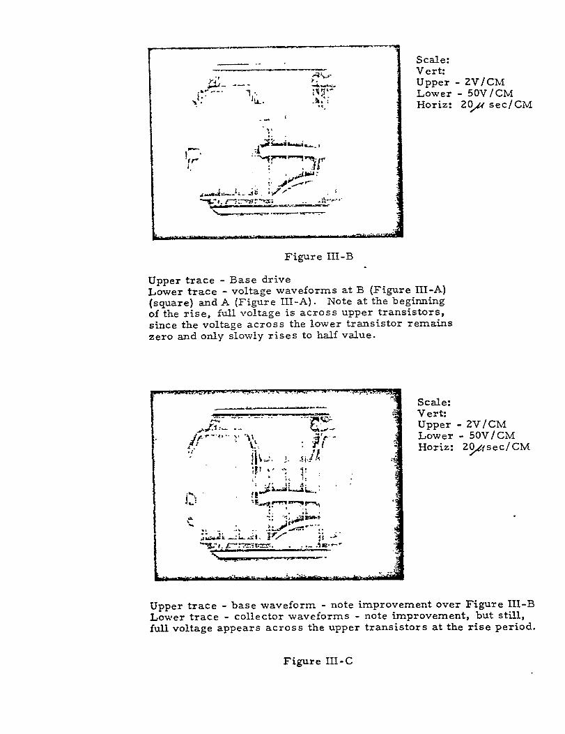
Early results were promising. However, continuing tests revealedthe difficulty in turning off both transistors in a pair exactly at thesame time. Even small differences caused the entire voltage toappear across a single transistor, resulting in its destruction.(See Waveform Figure III-B.)
Some improvement was made in this condition when the driver trans-formers were rewound, exercising particular care to insure symmetryand uniformity; however, small differences persisted. (See Fig. III-C.)
DRIVE
Figure III-A
Serial Transistors (Continued)
Capacitor and inductor equalizing networks were installed across the seriespairs with further improvement. Although DC biasing of the higher leveltransistor was considered, to insure automatic cutoff when the lower one wasswitched off, this approach was discarded due to the excessive heat and powerwasted in the bias circuit. Analysis of test data indicated that this systemcould, with care, be refined to produce a supply of the required capacity.
Para l le l Conf igura t ion
Since a number of new transistors having higher voltage and current ratingshad appeared in recent months, a new literature search was accomplished inApril , 1973. As a result , several new transistors were obtained and evaluatedOne of these, the General Electric D56W2, appeared promising, being ratedat 1400 volts at 5 amperes under the required operating conditions. However ,this transistor was found to have such a low gain as to make it useless for thisappl ica t ion .
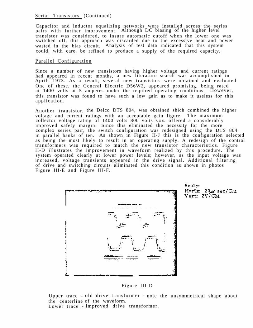
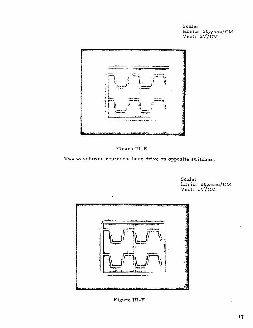
Another t rans is tor , the Delco DTS 804, was obtained shich combined the highervoltage and current ratings with an acceptable gain figure. The maximumcollector voltage rating of 1400 volts 800 volts S U S. offered a considerablyimproved safety margin. Since this eliminated the necessity for the morecomplex series pair, the switch configuration was redesigned using the DTS 804in parallel banks of ten. As shown in Figure II-J this is the configuration selectedas being the most likely to result in an operating supply. A redesign of the controlt ransformers was required to match the new t rans is tor character is t ics . F igureII-D illustrates the improvement in waveform realized by this procedure. Thesystem operated clearly at lower power levels; however, as the input voltage wasincreased, voltage transients appeared in the drive signal. Additional fi l teringof drive and switching circuits eliminated this condition as shown in photosFigure III-E and Figure III-F.
Upper trace -the centerlineLower t race -
Figure I I I -D
old dr ive t ransformer - note the unsymmetrical shape aboutof the waveform.improved dr ive t ransformer .
.
Serial Transistors (Continued)
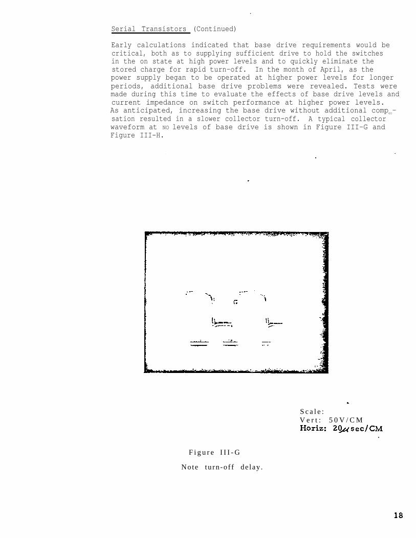
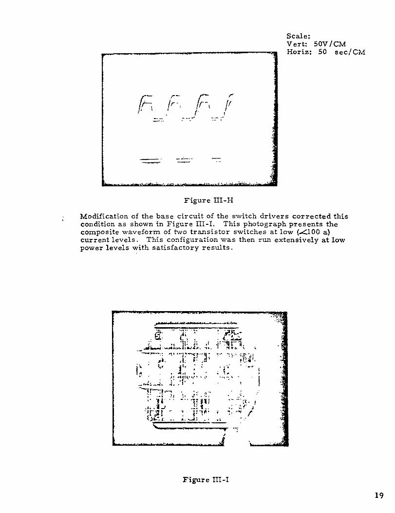
Early calculations indicated that base drive requirements would becritical, both as to supplying sufficient drive to hold the switchesin the on state at high power levels and to quickly eliminate thestored charge for rapid turn-off. In the month of April, as thepower supply began to be operated at higher power levels for longerperiods, additional base drive problems were revealed. Tests weremade during this time to evaluate the effects of base drive levels andcurrent impedance on switch performance at higher power levels.As anticipated, increasing the base drive without additional compen-sation resulted in a slower collector turn-off. A typical collectorwaveform at NO levels of base drive is shown in Figure III-G andFigure III-H.
F i g u r e I I I - G
Note tu rn -o f f de lay .
S c a l e :V e r t : 5 0 V / C M
.

Serial Transistors (Continued)
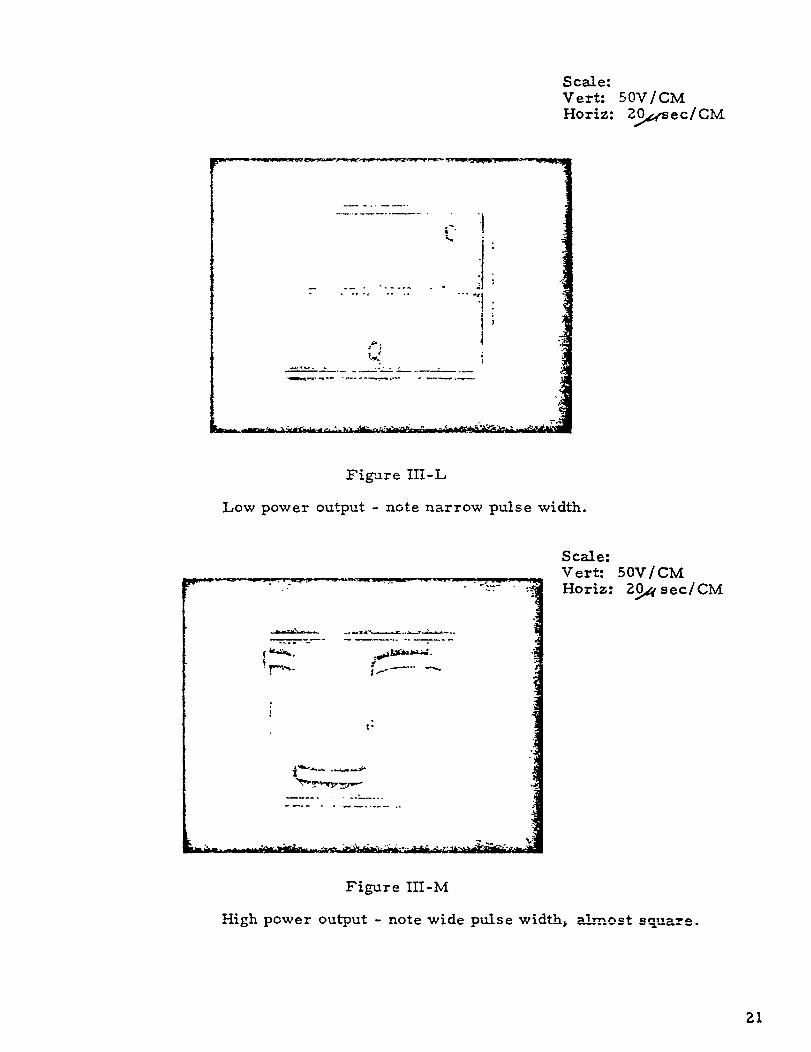
A new problem was encountered at high power operation. As shownin Figure III-K, a phase stift was encountered between the primaryand secondary of the power transformer which did not appear at thelower levels. As is shown in the photo by vertical line A, the leadingedges of the secondary low power pulses are coincident in time withthose of the primary at time B, a delay is seen between the leadingedges of the primary and secondary. Analysis of this condition in-dicated this condition to be the result of unbalance existing in the powertransformer. A new transformer was wound which corrected this shift.Photos of low and high power output signals showing the resulting sym-metry and transient free waveforms are presented in Figures III-Land III-M.
Scale:Vert: 50 V/CM
Figure III-K
20

c) Silicon Controlled Rectifiers
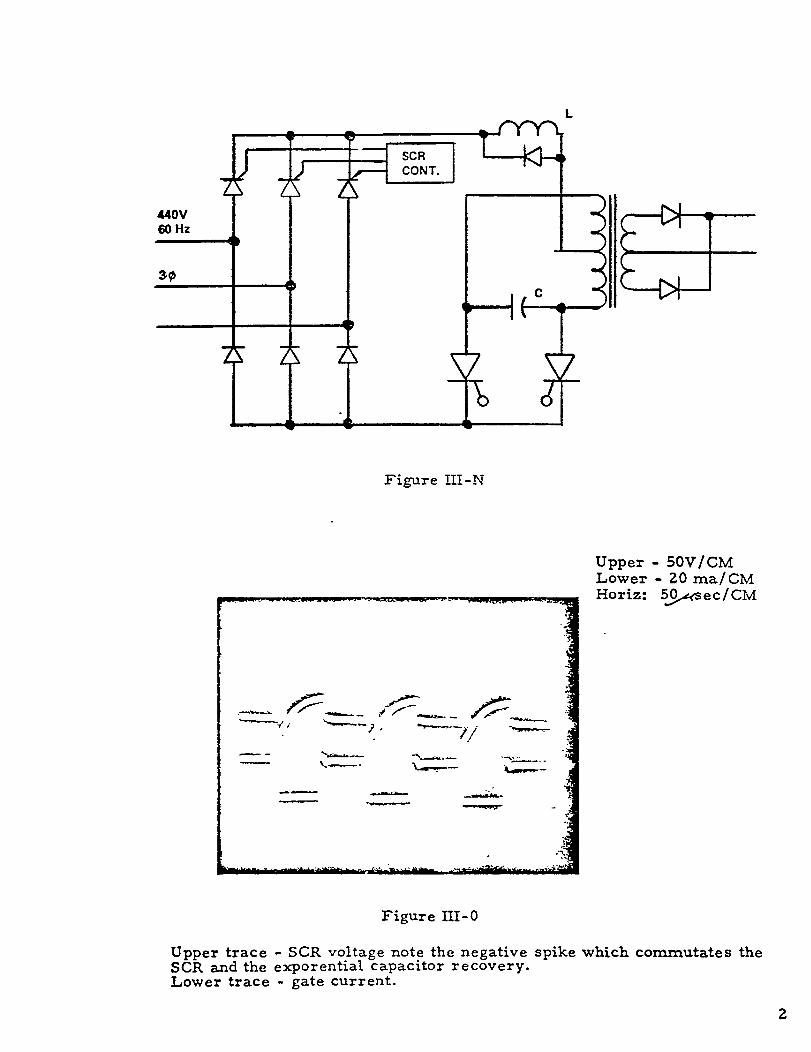
Unlike the transistor, the SCR’s only function is that of a switch.The SCR is turned on by a current pulse to the gate lead; the devicethen conducts anode to cathode. The main disadvantage of the SCRis that it is not as simply turned off; the SCR is turned off only bysome other component that either bypasses or interrupts the currentin the SCR. Most commercial applications involve the AC line, andthe alternating current is used to turn off or commutate the SCR.
The heart of the investigation of SCR’s consisted of solving the com-mutation problem since SCR’s are available with high voltage andcurrent rating. In all cases, however, inverter type SCR’s were chosedue to their higher frequency characteristics. The SCR used in thesubsequent investigations was the GE Cl59PB.
The first SCR circuit in’estigated was the coventional capacitor com-mutated circuit shown in Figure III-N. This circuit incorporates linecommutated SCR’s as an input switch. Two inverter SCR’s are usedin a certertapped inverter configuration.
One of the basic problems of this circuit is that in order to commutateone SCR off, the other must come on. This does not allow for vari-ability of welding current or voltage. The line commutated SCR’s werethen attempted to be used as phase control SCR’s, thus varying the DCvoltage to the inverter. Through calculations, it was observed that the
filtering required between the line SCR’s and the inverter would be quitheavy. This is due to the 60 HZ frequency of the AC line.
This SCR circuit was operated successfully under load; the waveformsare shown in Figure 111-0. However, under no-load conditions therewas no current to cause the commutating capacitor to recover. Theresult was that both SCR’s would fail to commutate, drawing excessivecurrent, resulting in their destruction. The only alternative was touse a dummy load to permit the capacitor to recover. This idea wasabandoned due to the excessive heat that would be dissipated in thedummy load.
Since open circuits exist continually in a welding operation, thiscircuit was considered unusable, not only because of its failure tocommutate properly, but because of its inability to result in a vari-able output.
22
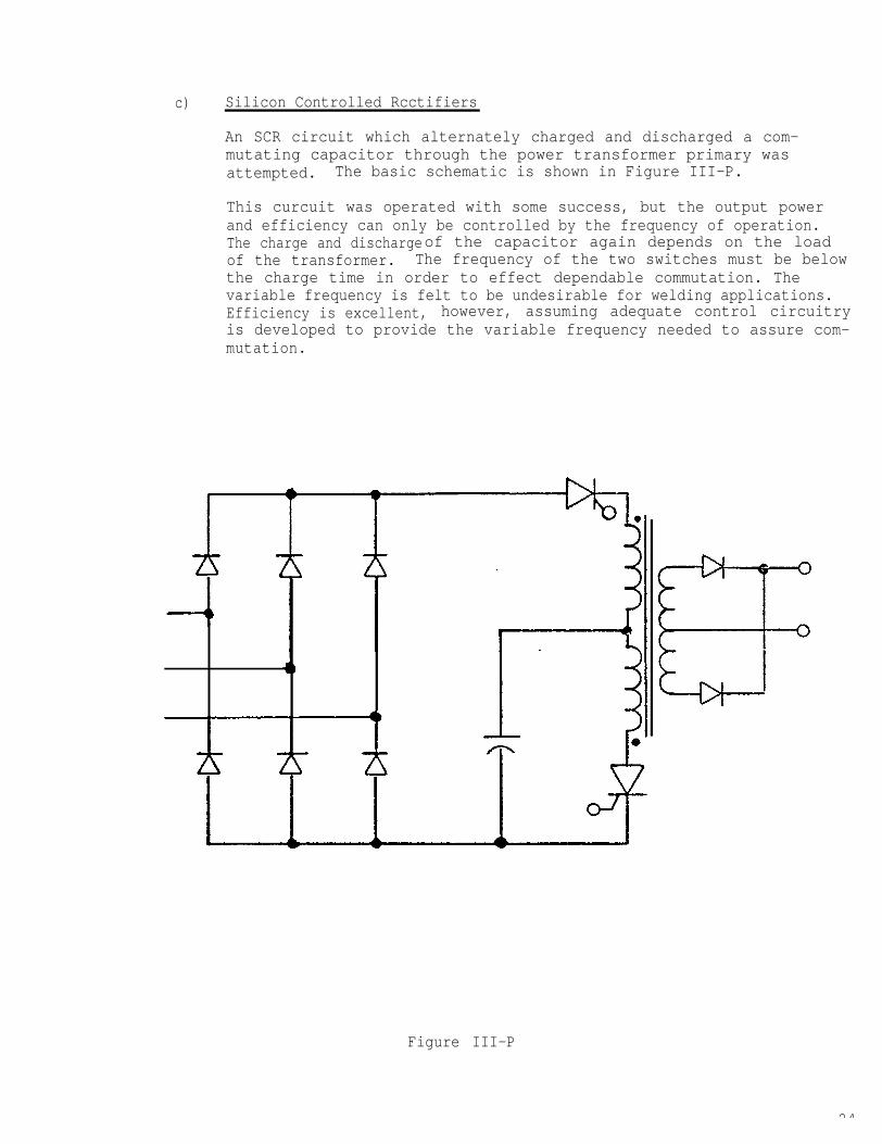
c) Silicon Controlled Rcctifiers
An SCR circuit which alternately charged and discharged a com-mutating capacitor through the power transformer primary wasattempted. The basic schematic is shown in Figure III-P.
This curcuit was operated with some success, but the output powerand efficiency can only be controlled by the frequency of operation.The charge and dischargeof the capacitor again depends on the loadof the transformer. The frequency of the two switches must be belowthe charge time in order to effect dependable commutation. Thevariable frequency is felt to be undesirable for welding applications.Efficiency is excellent, however, assuming adequate control circuitryis developed to provide the variable frequency needed to assure com-mutation.
Figure III-P
24
c) Silicon Controlled Rectifiers
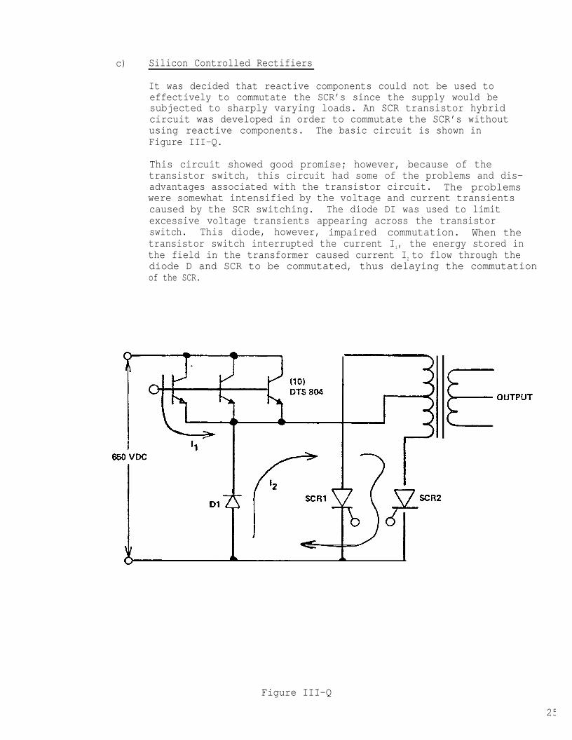
It was decided that reactive components could not be used toeffectively to commutate the SCR’s since the supply would besubjected to sharply varying loads. An SCR transistor hybridcircuit was developed in order to commutate the SCR’s withoutusing reactive components. The basic circuit is shown inFigure III-Q.
This circuit showed good promise; however, because of thetransistor switch, this circuit had some of the problems and dis-advantages associated with the transistor circuit. The problemswere somewhat intensified by the voltage and current transientscaused by the SCR switching. The diode DI was used to limitexcessive voltage transients appearing across the transistorswitch. This diode, however, impaired commutation. When thetransistor switch interrupted the current I1, the energy stored inthe field in the transformer caused current I2 to flow through thediode D and SCR to be commutated, thus delaying the commutationof the SCR.
Figure III-Q
25

c) Silicon Controlled Rectifiers
Various other commutation schemes were investigated at lowerpower levels. A summary of the results are presented in thefollowing discussion. One manufacturer has broken down thevarious methods into six basic categories. For ease of discussion,this classification will be used in this report
Class A
Class A commutation depends upon resonating the load to bringabout S CR turnoff. An LC resonant circuit is used for this pur-pose which carries the full load current. For this reason, theresonant self-commutation is most suited to frequencies above1 KHz. The output current is nearly sinusoidal with a corres-ponding low initial di/dt.
Characteristics of this circuit were found to be good output wave-form with excellent load regulation. It operates well into an opencircuit, as well as a variety of reactive loads. Some problems wereencountered with operating this system in a variable pulse widthmode, due to the resonant circuit requirements.
Class E
This method is similar to the above in that it uses an LC circuit toachieve commutation. Regulation is accomplished by time ratiocontrol. This circuit is of limited use, one example being theMorgan chopper. Some problems encountered were circuit in-stability and transients resulting from the reactive components.Regulation was difficult to achieve, and excessive sensitivity toload fluctuations was noted. Although these limitations can be over-come through the use of appropriate techniques, the approach wasfound to be generally unsatisfactory for the desired applications.
Class C
This is the simplest of the commutation systems, using a capacitoror L-C circuit switched by the load carrying SCR. The best knownexample is the McMurry-Bedford Inverter. Optimum values ofL and C are derived from the following equations:
In addition, an Ott filier may be used to elimainate harmoliics. Goodregulation may be achieved with this circuit; however, due to theL-C commutation components, this circuit is best used at frequencies
Class C (Continued)
below 1 KHz. In practice, difficulties were encountered in main-taining commutation and in achieving the desired efficiency andregulation.
Class D
In this method, an auxiliary SCR is used to switch an L or LCcircuit. High efficiencies may be achieved with this circuit, asthe commutation energy may be transferred to the load. Dutycycles of up to 80% may be realized. Puise width modulationis readily achieved, and the circuit works well at high frequencies.One example of this approach is the Jones chopper. The test cir-cuit operation agreed closely with the literature and with predictedfigures. This circuit was considered to be one of the more prom- ising for use on the welding power supply.
Class E
Class E commutation is achieved through theoff pulse. Although this circuit is not widelyrequirement for additional components, it isciencies and is readily adaptable to the pulse
use of an external turn-used, due in part to thecapable of high effi-width modulation system
selected for use in this application. Some progress was achieved inoperating a pulse commutated system.
Class F
This is the most basic of SCR commutation systems, in which thenormal operation of an AC line as the line voltage in changingpolarity automatically results in turning off the SCR. Since it de-pends on the AC input for commutation, its use is limited. Forthis application (after rectification of the 440 VAC 60 Hz 3Ø line),there is no line; therefore this method is not applicable.
D) Comparison: SCR's Vs Transistors
Since reasonable success was achieved with transistor switches, itwas decided that the transistor bridge circuit offered the best alter-native for achieving a demonstrable unit at the termination of thisproject. However, it should be noted at this point that if SCR controlproblems could be solved, a more economical, simple design wouldresult. To provide a timely demonstration of the feasibility of thehigh frequency approach, the full effort was directed toward an alltransistor unit.
Some of the advantages and disadvantages of the SCR's and transistorsare tabulated in Figure III-R. There are only two disadvantages withSCR's: lack of l-amiability and lack of adequate switch control. These
SCR’s as the switching elements.
27

E) Control Circuitrv Design
In order to drive the switching circuits in the correct phase andduration, control signals must be generated and conditioned bybuffer drivers. It is also necessary to provide a means of se-lecting the maximum current and to provide for control by a footpedal. Included in this section is the feedback curcuit which sensesthe supply output current and maintains it at a constant level,regardless of variations in arc length.
Operational Amplifier Control System
The first approach to switch control utilized operational amplifiersconnected in several configurations to generate the necessary con-trol functions. This circuit operated as required, however, someinstability was noted in the frequency control section. A completecircuit schematic is presented in Figures III-S to III-V.
Digital Logic
Due to the stability problem and to the inherent complexity of theoperational amplifier system, a digital logic circuit was developedwhich performed the same function. This approach, due to its sim-plicity and reliability, was selected for use in the final power supplyconfiguration. A schematic diagram of the final circuit is presentedin Figure IV-E and IV-F of the next section.
Phasing Considerations
The first switching circuits utilized four transistor switch sectionsarranged in a bridge configuration. This system requires that alter -nate circuits be switched on simultaneously to provide a currentreveral in the transformer primary. The period during which bothswitch sections are turned on, and during which the transformerprimary is drawing current in one direction, is a variable which con-trols the amount of current available at the output. Although thiscircuit works well in terms of current control, some problems wereencountered during the quiescent, or non-switching period. Due tothe fact that the primary of the power transformer was left floatingduring this interval, excessive transients and waveform distortionwere produced. To correct this condition, a modified switch cyclewas implemented which maintained the transformer either in anenergized or a grounded condition at all times. Original and mod-ified sequences are presented in Figure HI-W a and b.
Further problems were encountered in achieving correct switch timingdue to transistor turn-off time. Referring to Figure III-W-a, it can beseen that if switches 1 and 2 or 3 and 4 are turned on at the same timeshort circuit currents will flow, resulting in extensive component damaAs a first approach to the problem, careful attention was paid to thebase drive circuits, insuring that the stored charge on the bases wasquickly swept out. The effect of excessive turn-off time is shown inFigure III-X.
29
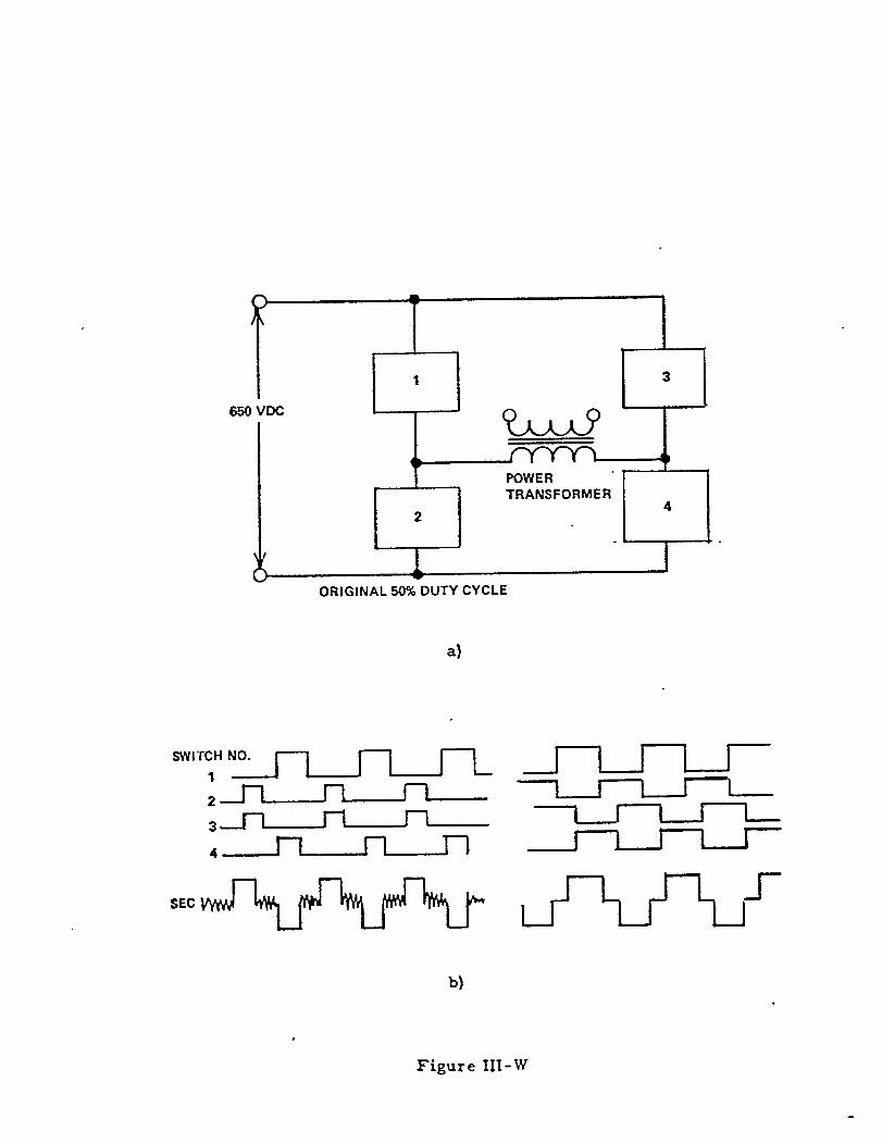

E) Phasing Considerations (Continued)
As shown, the assymmetr ica l cont ro l s ignal compensates forswitching delays, completely eliminating the undesired overlap.This delay was ultimately incorporated into the switch base drivec i r c u i t .
Buffer Drivers
The function of the buffer drivers is to convert the low level controlsignal from the logic to a larger signal having sufficient currentcapacity to drive the switch banks. To accomplish this, two medium-power transistors are connected in a Darlington configuration oper-ating from +24 volts. The output is transformer coupled to the basedr iver c i rcui ts . Ferr i te cores are used for the dr iver t ransformers .
Feedback Circui t
The feedback circuit performs several functions:
Senses the output current and maintains it at the selected level.a . Provides current l imiting during output short circuit conditions.c . Compensates for input voltage fluctuations.
C u r r e n t s e n s i n g i s a c c o m p l i s h e d b y i n s e r t i n g a f i x e d r e s i s t o r o f kvalue in series with the output circuit. This shunt res is tor i s pre-cisely calibrated to provide a known voltage drop for a given currentthrough the res is tor . A low-level voltage is therefore generated,which is proportional to the output current. This voltage is applied
where it is compared with a level estab-lished by the current select switch. Any difference in levels resultsin an error output from the operational amplifier, which is propor-tional to the amount of current deviation. This output, applied to thecorrect terminal of the delay multivibrator in the control circuit ,results in a shift in switch phasing which restores the current to itscorrec t level .
Since il l tering is required on the operational amplifier input, theresponse of the circuit is not instantaneous. C u r r e n t t r a n s i e n t sof less than several cycles duration will therefore not be correctedby this circuit and must be handled by other means. This delay canbe made adjustable so as to allow the operator to select the responserate most suited to this operation.
The foot pedal is so connected as to allow the operator to vary thearc current between zero and the maximum as established by these lec tor swi tch .
32

F) Transformer Design
The transformer design is the heart of the weight reduction solutionThe core area, windings, exitation and frequency are related in thefollowing formula (square wave exitation):
where V =N =A =B =f =
1 08V = 4 N A B r f
peak value of the square wave (volts)number of primary turnscross sectional core area (CM2)core flux density (gauss)frequency of applied square wave (Hz)
The formula can be rewritten as:
NA = 108v
4 B f
The product NA is representative of transformer weight copper(N as turns) and core (A as area). Since V is determined by 440vline (650 VDC rectified) and B is limited by the saturation flux of thecore material, the frequency must be increased in order to reducetransformer weight. Grest care must be taken in high frequency transformers to minimize core loss since core losses are roughly propor-tional to the square of frequency.
The first transformer was wound on a commercially available ArnoldEngineering core It was the only commercial core large enough(3 1/2" ID). The core is permalloy type core containing molybendumand nickle along with ferrous material.
First tests on the transformer were unsuccessful. The high nicklecontent causes a very low permeability in the core material; thismakes it unsuitable for transformer applications.
The next transformer was wound on a specially made core obtainedfrom Ceramic Magnetics of New Jersey. The dimensions were5" ID 7" OD, 1" high (this is a core area of 1 sq. in. or 6.45 CM2).The transformer was wound in house; the windings were somewhatloose, and considerable leakage inductance was observed. Therewere 175 primary turns and 11 secondary turns wound bifilar.
First tests on the second core were satisfactory. The transformerefficiently transmitted. The power, however, due to the excessiveleakage inductance, semiconductor damage was observed, plusregulation was poor; the transformer exhibited excessive "drooping"characteristics. Steps were taken to minimize the inductance.
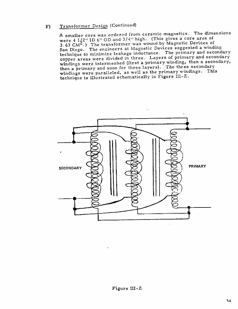
F) Transformer Desires (Continued)
The effect of the tight windings and the intermeshed primary andsecondary was approximately a 70% reduction in the leakage in-ductance. The transformer then efficiently transmitted the energyfrom primary to secondary with a considerably reduced "drooping"characteristic.
The material used in the Magnetic Ceramics cores was called MN60,which is a manganese and ferrite alloy. The core had high flux den-sity value (5600 gauss) and high permeability (about 10,000). Thesecharacteristics, in conjunction with low core and hysteresis loss,make this an excellent high frequency power transformer material.
G) Mechanical Packaging
Minimum size and weight were the primary considerations inpackaging this power supply. Heat sink selection and a packagingconcept were the major considerations. Heat dissipation was in-vestigated first. The major heat producing components producing85% of the heat dissipation, were the (1) input bridge, (2) switchingcircuits and (3) output bridge. The basic heat sink design andcooling requirements were designed around these components. Theremaining components with relatively small power dissipation wereto be mounted and heat sinked internally to the case.
Since as much surface area as possible would need to be reservedfor heat sinks, the external interface components, such as switches,indicators, the meter and output connection, were located on thefront panel. Possible stacking of power supply units for paralleloperation was also kept in mind for future units. This considerationalong with the fact that there will be dead air space on the bottom ofthe unit, made it undesirable to consider the top and bottom for heatsinking. This left the surface area of three sides for cooling.
Heat sinking to be used must be one sided or else arranged in amanner so as to keep all wiring internal to the case and providefor ease of sealing and exposed electrical conductors or connectors.All external heat sinking will be connected to a common ground toeliminate electrical shock hazard. Electronic components mustbe insulated from the heat sinks, thus increasing thermal resistancebetween component case and heat sink. Considerations such as thesmust be made in the thermal analysis.
A survey of available heat sinks was made and literature wasobtained from the following manufacturer:
Republic - TOR Gardena, CaliforniaThermalloy Inc. Dallas, TexasInternational Rectifier El Segundo, CaliforniaWakefield Engr. Inc. Wakefield, MassachusettsAstrodyne Inc. Wilmington, MassachusettsDelbert Blinn Co. Pomona, CaliforniaIERC Burbank, California
G) Mechanical Packaging (Continued)
The majority of available heat sinks are extrusions, which can becombined to suit the component sizes and requirements. Severalapproaches were considered for cases such as 1) thin walledaluminum casting with cooling fins, 2) a combination of aluminumheat sinks extrusions bolted to a skeleton frame, or 3) possibly acombination of aluminum (extrusions) welded together to form aone-piece box structure. Also to be considered would be specialextrusions made to suit this application. Because of cost, avail-ability and ease of disassembly, it was decided to select standardheat sinks and bolt them to a frame structure for the first packagedbreadboard unit. This would help minimize the time to assemble thebreadboard for test at possibly some sacrifice in weight and size.In further refinements, a more compact, lighter weight design couldbe achieved. On the first breadboard, water tight sealing was notimposed. However, all exposed components were to be covered andinsulated, with the result being a completely enclosed unit.
The transformer, because of its size and weight, is a primary con-sideration of the components to be mounted internally. It mustbe firmly mounted to the structure for ruggedness and convenientlymounted for making electrical connections. It must be low andcentrally mounted because of its effect on the center of gravity.
With these considerations, two approaches to packaging were con-sidered for the breadboard.
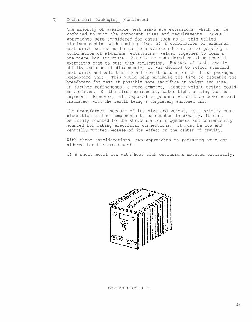
1) A sheet metal box with heat sink extrusions mounted externally.
Box Mounted Unit
36
G) Mechanical Packaging (Continued)
Considerations of this type of package:
(a) Need rigid box structure.
(b) Handle must be rigidly attached and an integral partof the structure.
(c) Sharp corners of extrusions are a problem and mustbe well rounded or protected so as not to be a hazard.
(d) Front and top panels and/or extrusions must be remov-able for access to internal circuitry.
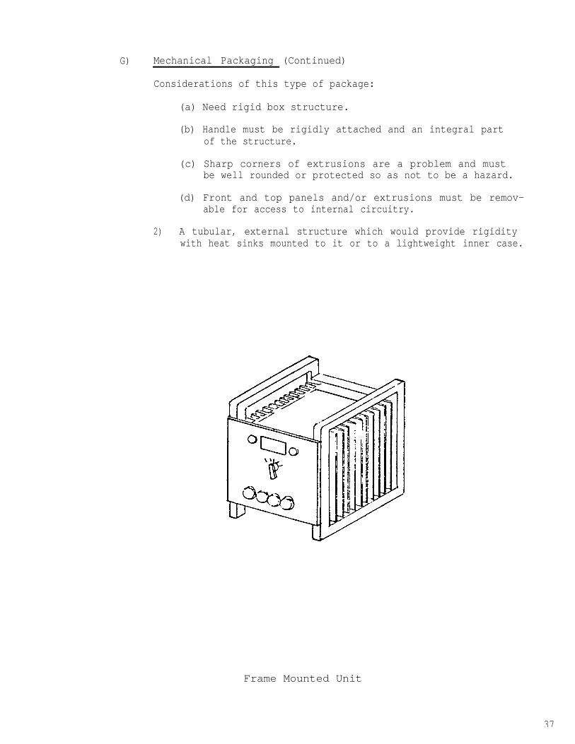
2) A tubular, external structure which would provide rigiditywith heat sinks mounted to it or to a lightweight inner case.
Frame Mounted Unit
37

G) Mechanical Packaging (Continued)
Considerations for this type of package:
(a) Frame would provide rigid protective structure.
(b) Handles to be a part of the frame.
(c) Tubular structure to protect thin fins of heat sinksfrom damage due to handling, and also providesprotection for sharp corners of extrusions.
(d) Provides a structure which can be easily adaptedto stacking.
(e) Internal case would be lightweight and of minimumstructure.
Of these two approaches, the latter appears to be the most favorable.Once heat sinks are selected, a final determination can be made. Ineither case, extrusions will be mounted vertically for maximumefficiency and some air space will be provided beneath and aboveeach heat sink to improve air flow.
H) Evaluation
During the investigative portion of this project, extensive testsof sub-assembl ies were made, compar isons were es tabl ished,and designs were chosen. This period corresponds to pointsone, two and part of three of the Plan outlined in the ObjectivesSection of this report.
The input rectifier was chosen as the originally designed three-phase br idge rec t i f ie r . There were virtually no other choicesfor this function. The transistors were chosen for the switchingcircuitry as being the best means of achieving success (ratherthan SCR’s) mainly for their control and advantages (Figure III-Rprovides a detailed comparison). The digital control circuitrywas chosen for i ts simplicity and accuracy, rather than the analogcont ro l . The transformer design was optimized during this periodas far as leakage inductance and efficiency are concerned. M e c h a n -ical packaging and heat sinking of the electronic components wasinvestigated for feasibili ty. Commercia l manufacturers of heatsinks were identified and analysis of their products was performed.A rough conception of the mechanical packaging was established.
39

IV Finalizing the Candidate Design
A) Further Development
As indicated in the previous section, the transistor switching cir-cuitry was selected as the most promising design for achieving ademonstrable unit within the time and budget limitations. Thisdecision was based on the initial research outlined in the previoussection. Full development of the transistor switching circuit wasrequired in order to have an operational system.
Figure HI-R lists some of the inherent problems of transistors forthis switching application; current and voltage ratings being the mostlimiting and severe problems, and also charge storage phenomenoncausing switching efficiency problems. Forty Delco DTS 804 tran-sistors were arranged in a bridge configuration as shown in FigureIII-W of the previous section.
First tests were promising using the candidate design. welding wasconducted using TIG and SMAW. However, random failures occurred,and significant switch heating was observed. The failures were attrib-uted to voltage and current transients occurring due to the time delayof the control circuitry. Since the feedback circuit is basically an integrator reacting to changes in average value of the current, the controlcircuit could not react instantaneously to short circuits. During thisperiod of control recovery, excessive currents and voltages appearedat the transistor, resulting in their destruction. It was decided, there-fore, that a subcycle current limiting would have to be incorporatedindependent of the control circuitry.
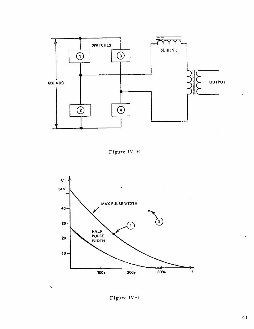
Resistive current limiters were impractical due to the excessivedissipation they would cause. Therefore, reactive current limiterswere used in the form of linear inductors and linear capacitors.The inductive current limiting was successful in reducing the semi-conductor failure. However, it had some undesirable characteristics.The inductor was placed in the primary line, as shown in Figure IV-H.
7.2 K Hz frequency, thus limiting the fundamental primary currentto 30 amps peak.
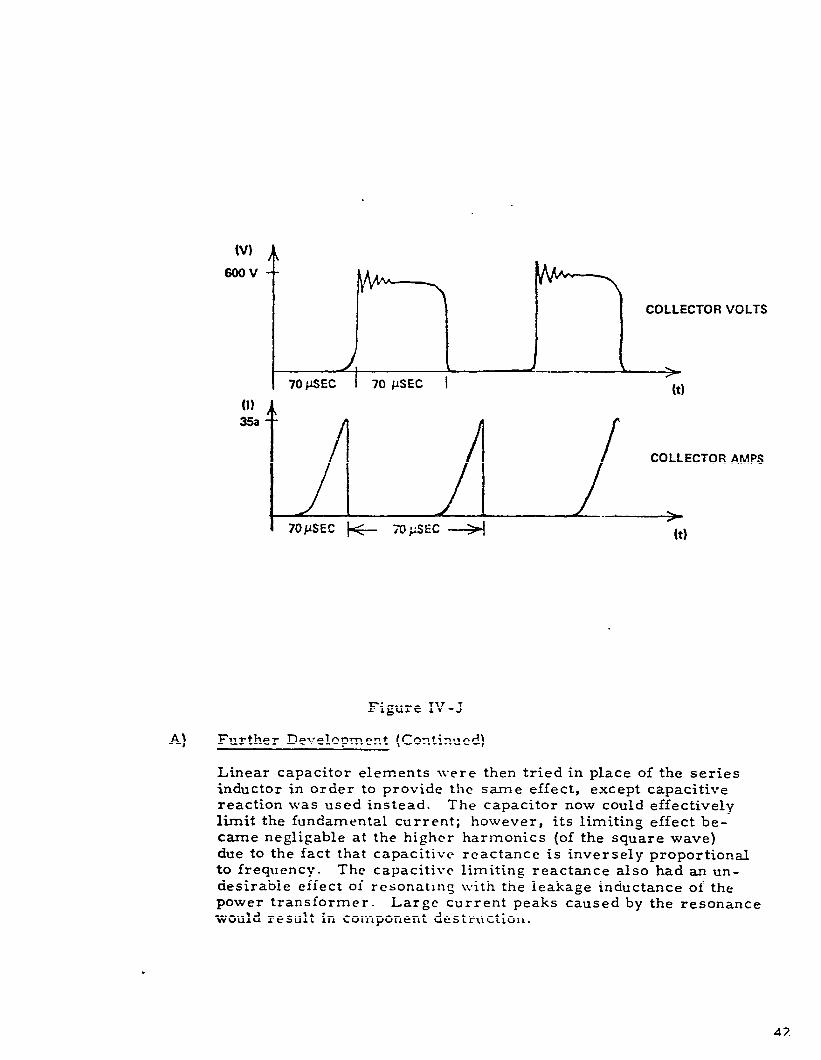
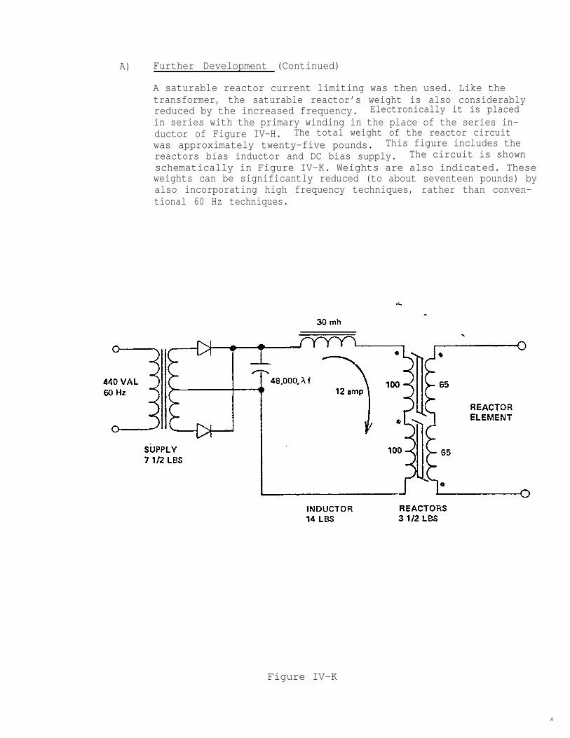
Due to the slight nonlinearities in the inductor, and the fact that sig-nificantly lower power levels in the 3rd, 5th and 7th harmonics werepassed, the inductor method of current limiting provided a V-I char-acteristic shown in Figure IV-1 that would be undesirable for weldingapplications. As can be seen, at an arc potential of 23V, only 150amps could be delivered (point 1). Point 2, 40 volts at 300a is farbeyond the capability of the unit. Also, the subcycle current wave- form contained high peaks at the end of the cycle, as shown inFigure IV-J. This is typical of inductive loads.
40
A) Further Development (Continued)
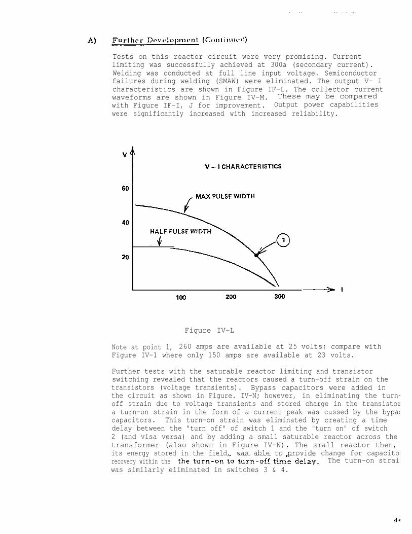
A saturable reactor current limiting was then used. Like thetransformer, the saturable reactor’s weight is also considerablyreduced by the increased frequency. Electronically it is placedin series with the primary winding in the place of the series in-ductor of Figure IV-H. The total weight of the reactor circuitwas approximately twenty-five pounds. This figure includes thereactors bias inductor and DC bias supply. The circuit is shownschematically in Figure IV-K. Weights are also indicated. Theseweights can be significantly reduced (to about seventeen pounds) byalso incorporating high frequency techniques, rather than conven-tional 60 Hz techniques.
Figure IV-K
4
Tests on this reactor circuit were very promising. Currentlimiting was successfully achieved at 300a (secondary current).Welding was conducted at full line input voltage. Semiconductorfailures during welding (SMAW) were eliminated. The output V- Icharacteristics are shown in Figure IF-L. The collector currentwaveforms are shown in Figure IV-M. These may be comparedwith Figure IF-I, J for improvement. Output power capabilitieswere significantly increased with increased reliability.
Figure IV-L
Note at point 1, 260 amps are available at 25 volts; compare withFigure IV-1 where only 150 amps are available at 23 volts.
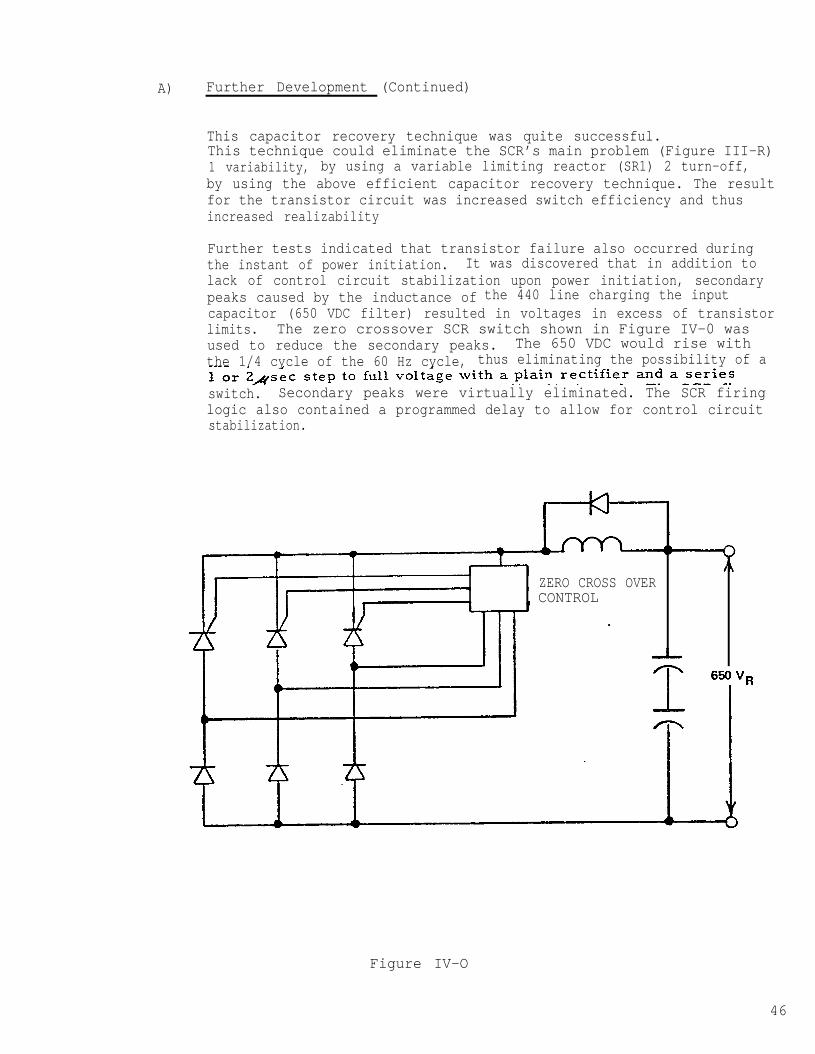
Further tests with the saturable reactor limiting and transistorswitching revealed that the reactors caused a turn-off strain on thetransistors (voltage transients). Bypass capacitors were added inthe circuit as shown in Figure. IV-N; however, in eliminating the turn-off strain due to voltage transients and stored charge in the transistora turn-on strain in the form of a current peak was cussed by the bypascapacitors. This turn-on strain was eliminated by creating a timedelay between the "turn off" of switch 1 and the "turn on" of switch2 (and visa versa) and by adding a small saturable reactor across thetransformer (also shown in Figure IV-N). The small reactor then, its energy stored in the field, was able to provide change for capacitorrecovery within the The turn-on strainwas similarly eliminated in switches 3 & 4.
A) Further Development (Continued)
This capacitor recovery technique was quite successful.This technique could eliminate the SCR’s main problem (Figure III-R)1 variability, by using a variable limiting reactor (SR1) 2 turn-off,by using the above efficient capacitor recovery technique. The resultfor the transistor circuit was increased switch efficiency and thusincreased realizability
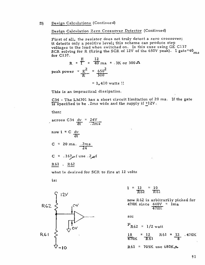
Further tests indicated that transistor failure also occurred duringthe instant of power initiation. It was discovered that in addition tolack of control circuit stabilization upon power initiation, secondarypeaks caused by the inductance of the 440 line charging the inputcapacitor (650 VDC filter) resulted in voltages in excess of transistorlimits. The zero crossover SCR switch shown in Figure IV-0 wasused to reduce the secondary peaks. The 650 VDC would rise withthe 1/4 cycle of the 60 Hz cycle, thus eliminating the possibility of a
switch. Secondary peaks were virtually eliminated. The SCR firinglogic also contained a programmed delay to allow for control circuitstabilization.
ZERO CROSS OVERCONTROL
Figure IV-O
46

A) Further Development (Continued)
During the period of "Further Development of the TransistorSwitches", the following transistor problems were eliminated:
1) Current peaks were eliminated by effective saturablereactor current l imi t ing . Power output and realizabilitywere a lso increased.
2) Heating due to stored charge was reduced by bypasscapaci tors and reac tor recovery for the capaci tor .Reliabili ty and efficiency were also increased.
3) SCR contactor was incorporated to reduce transientsand provide for smooth turn-on.
B) Elect ronic Circui t Diagrams
See Figures III-S, T, U and V.
The following paragraphs of this section are devoted to the docu-mentation and explanation of the unit resulting from this research.The circuit diagrams are first followed by theory of operationsand design calculations.
c ) Theory of Operations
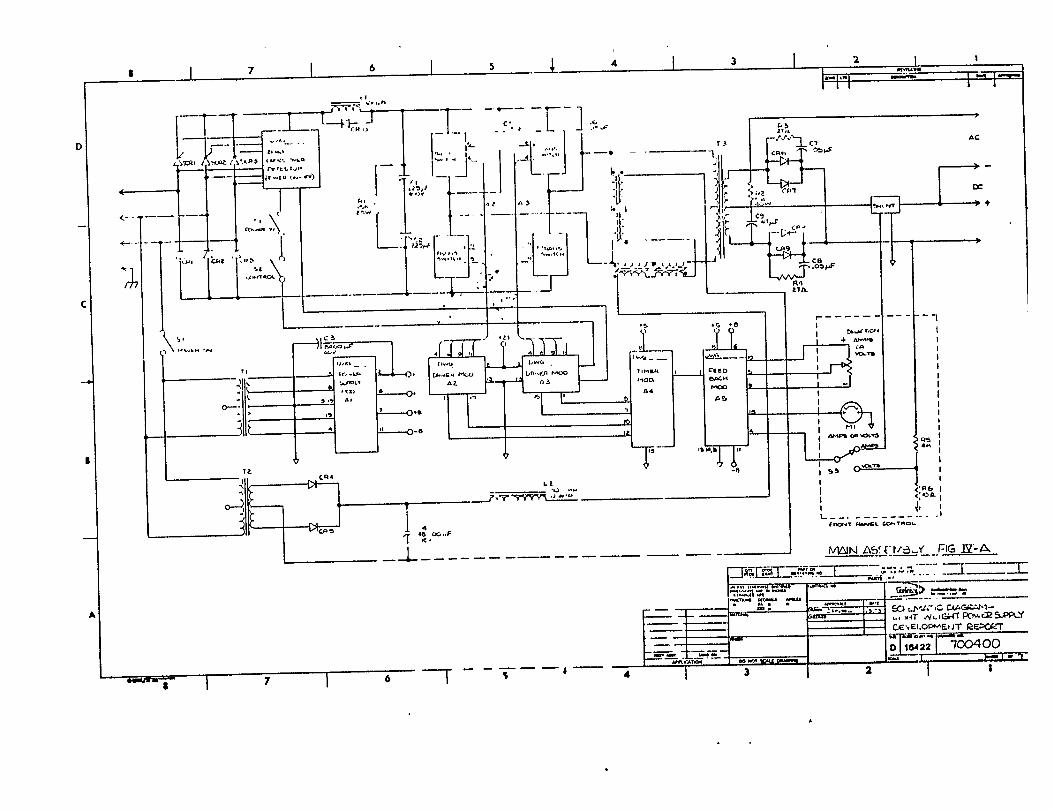
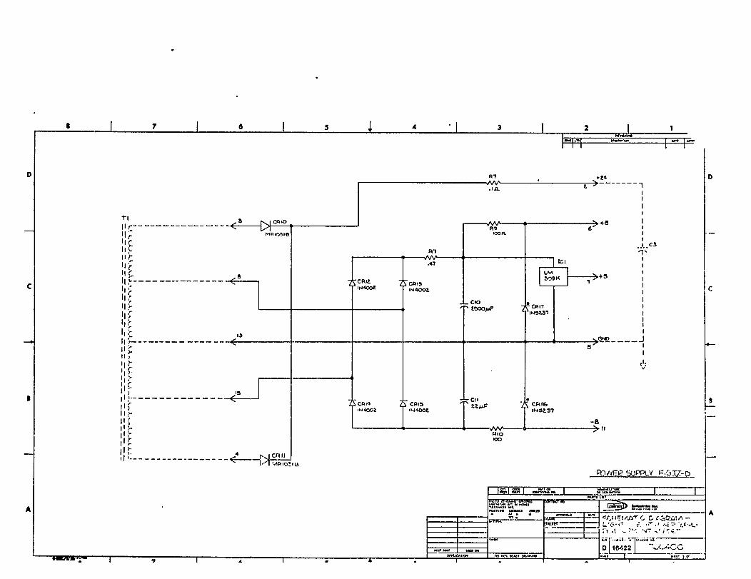
Refer to drawing Number 1000, Figure IV - A
This is a schematic of the main assembly. The basic diagram shownin Figure IV-4 can be visualized in this main assembly drawing. Theinput rectifier consists of SCR 1, SCR 2, SCR 3 and D 1 to D 3. Nextcomes the fil ter L1, Cl and C2; then the transistor switch bridgeconfiguration. The transformer network consists of SR 1, SR 2 andTR 3; the output rectifier consists of D 6 to D 9. The feedback loopcan be seen starting with reference signal at RRl and current feed-back module A 5 compares the reference and controlled signs.giving an error signal to the Timer Module A4. The Timer modulethen controls the driver modules A 2 and A 3 which control the tran-sistor switches 1, 2 , 3 a n d 4 SCR 1 to SCR 3 perform theadded function of an on/off switch, a lightweight version of a contactor.The SCR’s are controlled by the zero-crossover detector (DWG No.1001) and S1 (power on) and S2 (contactor). TR1 and the power supplymodule Al derive and regulate the logic supplies from the 440 VAC60 Hz line. TR2, D4, D5, C-1 and L2 provide the DC bias to thesaturable reactors SR1 and SR2 (12 amps).
D) Design Calculations - Some of the major design calculations arepresented in order to give further insight into the electronic operationof the system. Refer to Drawing No. 1000, Figure IV-A.
47


D) Design Calculations (Continued)
use 30 mh
Zero Crossover Detector
Refer to Drawing No. 1001, Figure IV-B. The primary function of themodule is to supply the gate pulses in proper time sequence to the SCRcontactor (SCR1 to SCR3, Drawing NO . 1001, Figure IV-A). The zerocrossover detector consists of a power supply (JR5, D33 to D36, C31,C32) and three similar SCR driver circuits, one for each SCR.
Basically, the SCR drivers must sense the positive leading rise ofthe 60 Hz 440 line sine wave, and fire the SCR as the sine wave c r o s s ethrough the zero volt level. This permits the 650 VDC supply to comeup "gradually" in a quarter cycle of 60HZ instead of instantaneously,which causes destructive peaks discussed in part A of this section.A4 and LM1301 is used as a comparator. Consider the SCR 1 first beingreverse biased by some negative voltage. A4 is then saturated at thepositive supply, the capacitor C34 then charges up to the full plus andminus supply through A-1 and TR6. D37 is a 4.7 V zener diode pro-tecting A4 against arbitrarily large negative voltages on the input R62.(This voltage can be as large as 650V.) C33 is a noise supressorwhose time constant (with R61, R62 and D37) is negligible as far ascircuit operation is concerned. The voltage on the anode of SCR1 thenrises to a positive value as the line voltage crosses zero. When thevoltage on the anode reaches +12V to insure anode current, the junctioof R61 and R02 reaches common (zero potential) and A4 switches tothe saturated state at the negative supply level. This causes a neg-ative pulse on the dotted winding of TRG due to the charge on C34.This supplies a positive pulse to the gate of SCR1 C34 then rapidlyd i s c h a r g e s .
The power supply is a critical part of the circuit operation. The inputpower comes from the 7000 Hz of a switch driver (A3 Figure IV-A,Dwg. 1000) via the power switch and the contactor switch. The supplyhas a 25 ms rise, due to the time constant of R59, C32 and R58, C31.Therefore, if any SCR has a positive voltage across it (blocking) whenthe switch is turned on, it will not fire because C34 cannot pass such agradual slope. The SCR will not fire until the anode potential crossesthrough zero in a positive direction. Thus, the input circuitry willnever be subjected to an input step voltage causing destructivesecondary peaks.
Design Calculation Zero Crossover Detector
First of all, it is important to point out why a simple resistorconnected anode to gate as follows won’t work:
50

D) Design Calcullations (Continued)
TR6
Since 40 ma are needed to fire C137 SCR’s, then the 20 ma availablefrom the LN1301 is insufficient. TR6 is a current step up. For 100%safety factor, I gate (pulsed) should be 80 ma.
or a 4:1 turns ratio.
This ratio also reduces the voltage from 24 to 6. Other components arechosen by selection.
Transistor Switch
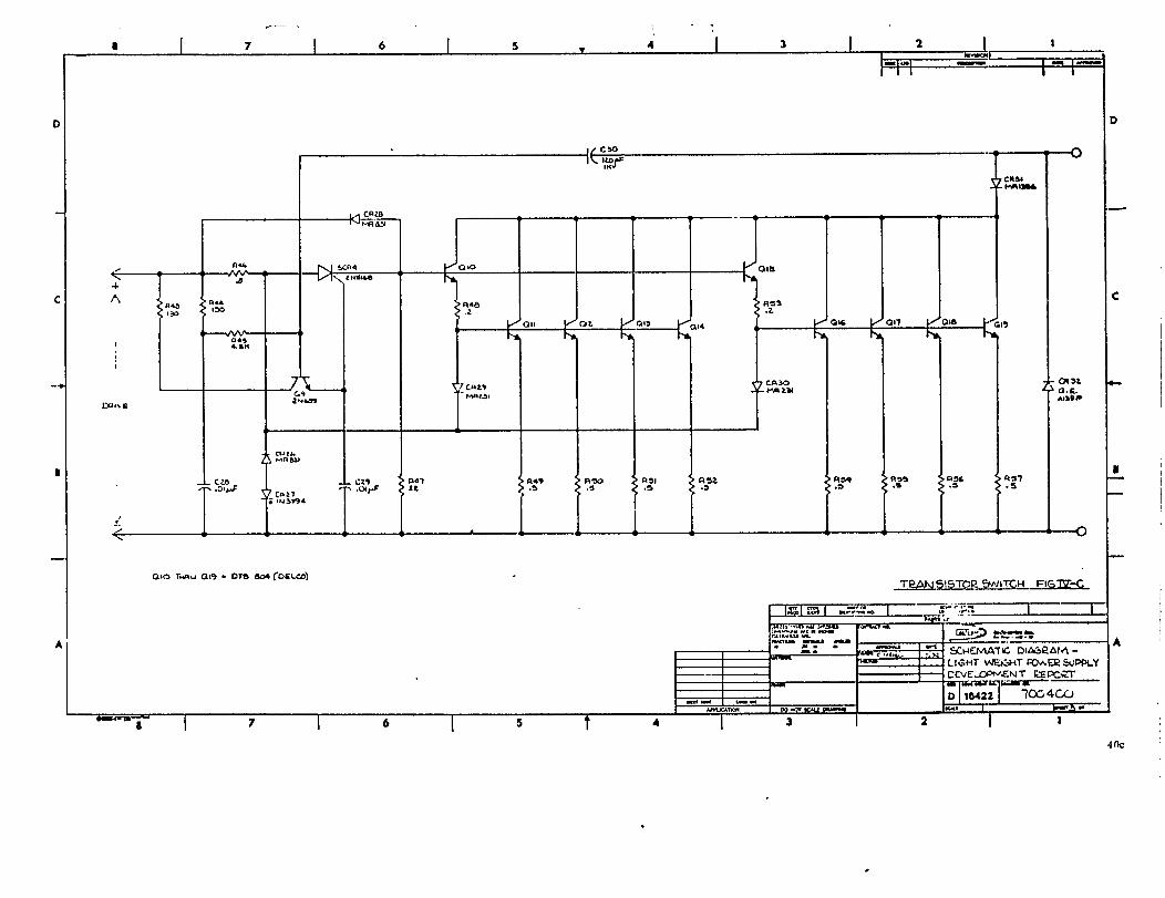
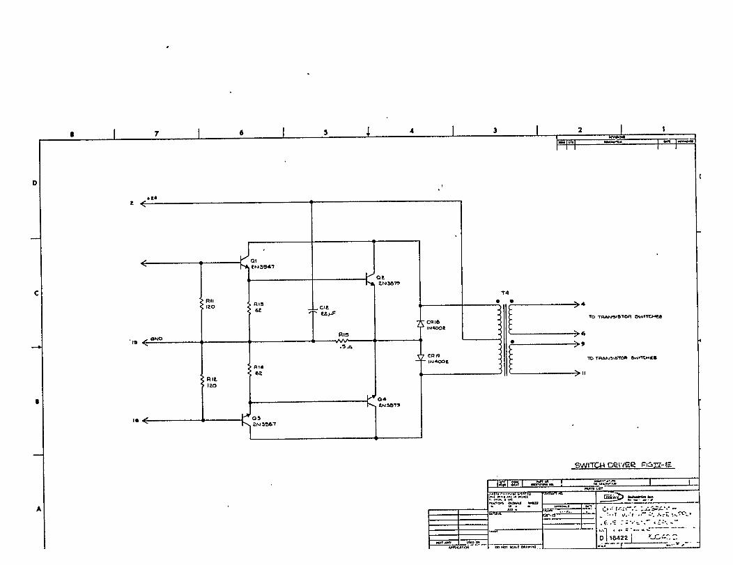
Refer to Drawing No. 1002, Figure IV-C.
The main function of the transistor switch is switch the current 30 ampsat 650 volts. Q1O through Q19 are DTS804 (Delco) transistors; theyhave a maximum collector current of 5a and voltage of 800v (SUS). Theare configured as a double darlington since at 3 amps the DC B is about4. One driver then dirves a bank of four with 3 amps base current de-livering 12 amps total collector current (3 amps per transistor). Therefore, all transistors, including the drivers Q1O and Q15, have equalloads. R49 through R57 are emitter resistors for current balancing.Since the switch drives reactive loads (SR1, SR2 and TR3), D32 is usedto conduct reverse currents. D31 prevents the transistors from beingoperated in a reverse mode when current is flowing through D32. D29
and D30 are used to sweep out stored charge in the transistor banksand D28 sweeps stored charge out of the drivers.
As was mentioned in the previous discussion on the main assembly
"turn-on" of switch, two, and vice versa, is needed to allow for capac-itor recovery of C5 (and C6) by reactor SR1. This display is pro-vided by the circuitry preceding the transistors (Figure IV-C) SCR4,Q9, C30 and related components. The input switch drive is a 6 voltpeak symmetrical square wave. The transistors Q1O and Q15 receiveddrive through SCR4 and R-46; however, SCR4 does not conduct until itreceives gate drive via Q9 and R43. With the positive edge of the drivesignal C28 is charged to - 6V (previous level of drive square wave). R4and C28 provide a fixed 4 sec delay in drive to Q9 (and thus the tran-sistors Q1O, R15). During this time, C5, C6 (Figure 4A) begin theirrecovery of discharge. Their recovery time is variable, depending onoutput load; the worst recovery is 30 sec. (see discussion on mainassembly, Figure IV-A). C30 senses the "negative sloping voltage(capacitor recovery) and feeds a negative current through R45, causinga negative voltage on the base of Q9, thus holding Q9 off. When thecapacitor (C5) is fully recovered, the voltage on the anode of D31 ceaseits negative rate of change of voltage, current stops through C30 andQ9 receives drive through R11 and R45. SCR4 drives the QIO and Q15,driving the whole switch on.
52


Logic Power Supply
Refer to Dralwing No. 1003, Figure IV-D.
The logic power supply's function is to supply the voltage at requiredcurrents to the switch drivers (Figure IV-E), the timer module(Figure IV-F, and the Feedback Amplifier circuit (Figure IV-G). Theoperation is straight forward. The regulators receive power fromTR1 9shown on Figure IV-A) whose secondary is centertapped 10 VACand 18 VAC secondary. The 18 VAC windings are full wave rectifiedby D1O and Dll; this unregulated line is filtered by C3 (shown on mainassembly Figure IV-A) and supplies 24 volts to the switch drivers(Figure IV-E). R7 is a surge limiting resistor. The 24 volt line israted at 4 amps. The 10 VAC windings are full wave rectified by D12to D15, and filtered by C1O and C R9, R1O, D16 and D17 are zenerdiode regulators which provide +8 volt lines for the feedback amplifier(Figure IV-G). The +8 volt lines are rated at 60 ma. IC1 is an LM309K voltage regulator for the 5 volt supply for the TTL IC’s in thetimer module (Figure IV-F). The five volt line is rated at .5 amp.
55

D) Design Calculations (Continued)
Secondary Turns
Q2, Q4
This is within Ic max of 2N3567.
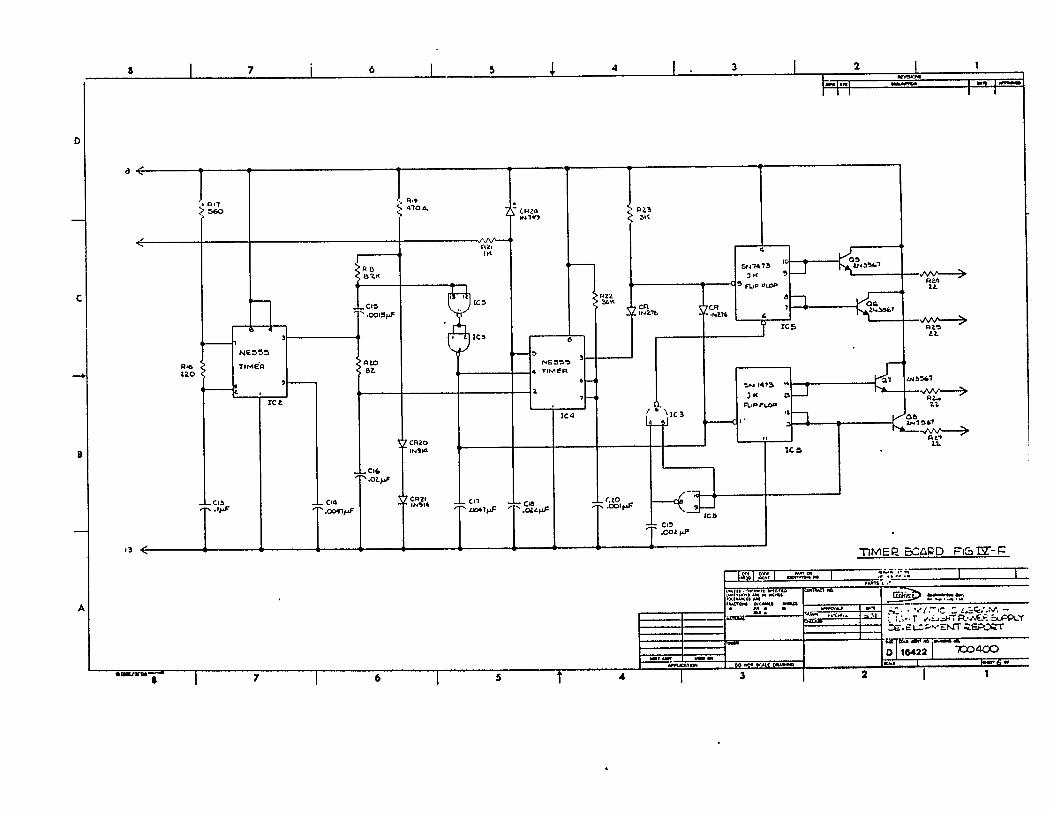
Timer Module
Refer to Drawing #1005, Figure IV-F.
The basic function of the timer module is to 1) set up 7000 Hz clockfrequency of the unit; 2) receive an error signal from the feedbackcircuit; 3) adjust the phasing of the transistor switches (see FigureIII-W and related discussion).
R16, C13 and IC2 make up an astable flip flop operating at 14 KHz.C15, C16, C17 and IC3 (1) and (2) perform waveshaping functions.R21 and C18 integrate the error signal and feed it to IC4, which isa voltage controlled time delay. The fixed clock and the delayedclock IC2, and IC4 respectively operate JK flip flops (IC5). TheJK flip flops drive emitter followers Q5 to Q8, which supply the lowlevel signal to the switch drivers. IC3 (3) and (4), and C19 performa phase locking function to insure that Q6 always lags Q8. The oper-ation can be more easily seen in a waveform progression shown inFigure IV-P. Waveform VC13 shows Cl 3 oscillating in a relaxationm o d e . VC16 shows C16 moderately degrading the square edges ofthe output of IC2. IC3 (2) shows a narrow one-shot pulse; this pulseis used to reset IC4 if necessary. Vc20 shows the voltage across C20;C20 charges through R22 to the voltage (control feedback voltage orintegrated error signal) at pin 5 at which time it discharges, creatinga time delay Ø which phases the signals to the switch drivers. If forsome reason Vc20 ncver reaches V pin 5 (very large error signal, forexample) then the reset pulse 1c3 (2) resets the timer. thus limitinga maximum phase separation of 180.
58

R22 C20
These components determine delay time Ø of Ic4 pin 3, Figure IV -P.
Since V pin 5 =
Other components are pul l -up res is tors or f i l te r ing capaci tors .
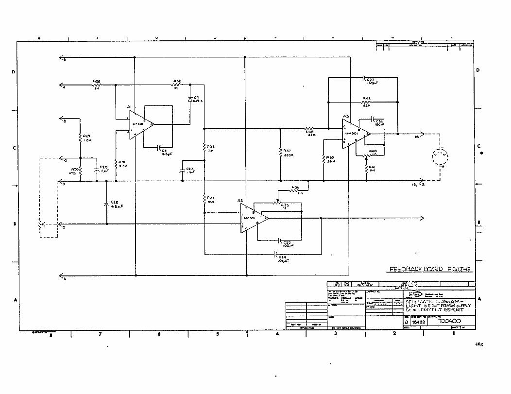
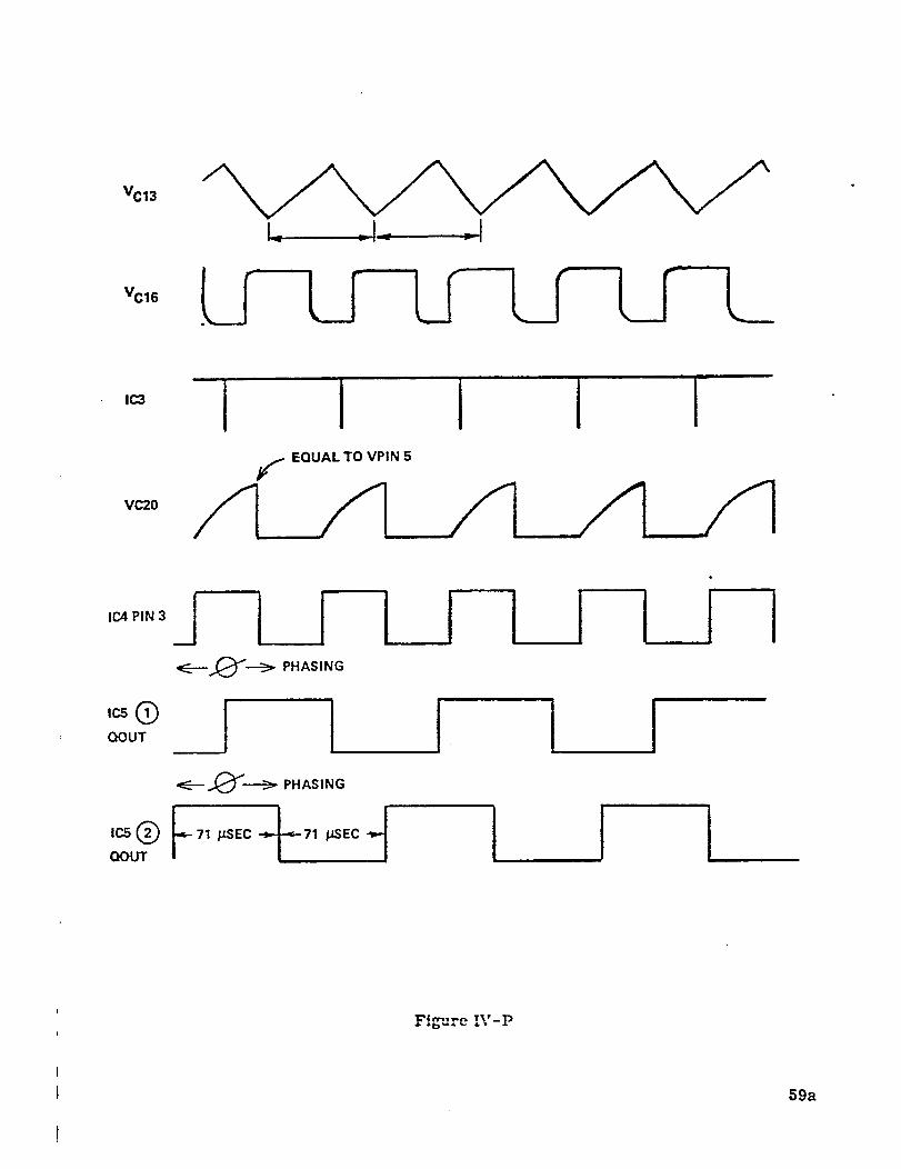
Feedback Board
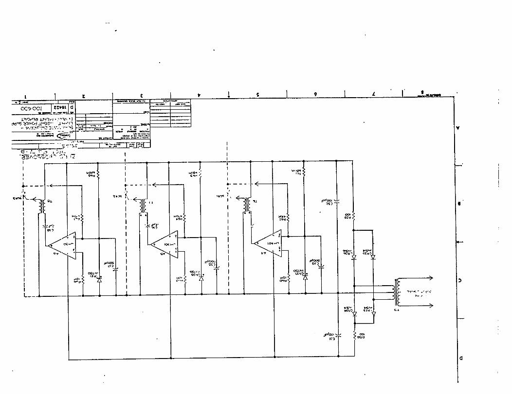
Refer to drawing #1006, Figure IV-G.
The basic function of this circuit is to convert a low level signal froma shunt, to a workable level for the timing module. Al is a losslessfull wave rectifier; it has the following transfer function:
When the input (pin 4 to R28) is positive, the output of Al saturatesnegat ive ly . D25 blocks the negative amplifier output and the signalpasses through R2S and R32 to the output. If the signal in is negativethe D25 is forward biased by the amplifier output and the circuit actsas a unity gain inverting amplifier, thus the output is again positive.A2 performs as the summing junction of the reference signal (pin 5)and the controlled signal (amps). A2 also performs a pure integrationmaking this a type 1 system with zero (or approaching zero) statice r r o r . The output of A 1 goes to the timing module. Since the outputof the full wave rectifier (Al) is high impedance, the amplifier A3 isa high input impedance (relative to 2 out of Al circuitry) unit gainamplifier used to drive the meter.
60

I V E ) Mechanical Design
1. Heat
An estimate was made of anticipated component heat dissipationfor purposes of thermal analysis and heat sink selection. Thisestimate is as follows:
1.2 .3.4.5.6.7.8.
Over load cont ro l c i rcui t ryInput bridgeTrans i t ion swi tchesOutput bridgeTrans fo rmer co i lControl logic and switch driverClipper NetworkVarious other components
50200390780
802080
n e g .
TOTAL 1600
Since approximately 85% of the heat dissipated is in the outputbridge, transistor switches and input bridge, they will be thepr imary cons idera t ions for a detailed thermal analysis. F o rpurposes of this ca lcula t ion , maximum ambient a i r was assumedto be 50 C (122° F). This would include the effects of maximumtemperature shopair possible being heated be adjacent powersupplied or related equipment.
a) Output Bridge
Preliminary calculations indicated that heat dissipation inthe output bridge would be a problem. AS a result theoriginal D09 size stud mounted type rectifiers were re-placed with GE A396 Press Pack type rectifiers. The presspack configuration allows for two sided mounting with theresul t be ing improved heat t ransfer character is t ics . T h e r m a lcharacter is t ics for th is device are :
GE A396 Press Pack RectifierMax Junction Temp 125CThermal Resis tance J -C 1 5 C / W a t t
Two rectifiers dissipating 780 watts amounts to 390 watts perr ec t i f i e r . Initial estimates of thermal resistance of a typicalpress pack type heat sink @ .18C/watt. Insulating washerswill be required between the components and the heat sink.Because of the high heat transfer conventional insulatingwashers were bypassed for beryllium oxide type which havesuper ior heat t ransfer character is t ics . Using a .062 thickberyllium oxide washer the size of the contact area of thepress pack rectifier and including contact resistance, a totalthermal res is tance of 12°C/watt per rectifier was calculated.
61

E) Mechanical Design (Continued)
a. Output Bridge (Continued)
A thermal rise calculation can then be made for each device.
max ambient temperatureheat sink T.R .18C/watt x 390 watt = 50Cinsulator T. R. .12C/watt x 390 watt = 70.2Crectifier T.R. .15C/watt x 390 watt = 58.5C
Total junction temperature 225.5C
As can be quickly seen, this greatly exceeds the rated maximum. allow-able junction temperature. To remedy this solution, it was decided toincrease the number of rectifiers to four instead of two. By parallelingthe devices, the heat dissipation per device would be cut in half, resultiin a calculated max junction temperature of 170C. This still exceedsthe rated temperature. However, after further evaluation and testingof the breadboard, the power estimates were reduced to about 100 wattsper device with four devices. This results in a maximum junctiontemperature of 113°C, which is below the maximum component ratingallowed for this device.
A heat sink was then selected which would provide the required heatdissipation. This extrusion was Thermally 6740 or equivalent Wakefiel3560, which are designed specifically for press pack mounting.
Wakefield 3560Weight 4.3 lb./ft.T.R. = .18C/watt (based on a pair of extrusions
14" long - two or more devices per assemblyto distribute heat. (See Wakefield Cat. No. 103,page 47).
Thermalloy No. 10888 compression clamps were used inconjunction with the heat sinks for proper mounting.
Transistor Switches
The switching circuits to be heat sinked consist of forty (40) TO3 casetransistors. These transistors conveniently fall into four groups of 10each. A quick layout indicates that 10 transistors arranged closelyin one row will fit within a 14" length with some room on the end formounting holes. Calculations are based on mounting one row of 10transistors along with 2-D04 diodes per heat sink. Heat dissipationis based on 13 watts per transistor.
Using a Thermalloy 6175 extrusion, a Thermal resistance of .56°C/wattwas calculated, based on distributed components.
The thermal rise calculation then becomes:
Ambient air temp 50CHeat sink rise .50°C/W x 130W 73CKapton insulators .5°C/W x 13W 7CCase to junct rise 1°C/W x 13W 13C
Total max Junct temp 143C

E) Mechanical Dcsign (Continued)
Transistor Switches (Continued)
This is well below the maximum allowable junction temper-ature of 200°C for the Delco DTS 804 transistors. Associatedcomponents mounted to the heat sink will contribute very littleheat.
Input Bridge
The input bridge consists of a set of three each syntronR34100 DO5 case size diodes and a set of syntronS34100 DO5 case six diodes. Power dissipation is 200 wattstotal or 34 watts per device. Thermal resistance is 1°C/wattand maximum junction temperature is 2000C.
Since there is less heat dissipated by three of these diodesthan a row of the 10 transistor switches, it was decided touse the same extrusion (Thermalloy 6175) for uniformity inpackaging and mount each set of diodes on a separate heat sink
2. Packaging
With the heat sinks selected and a basic concept in mind, a packagelayout was made. Heat sinks were arranged in a compact con-figuration with the height being determined by the transistor switchconfiguration as 14 inches. Heat sink layout is shown in Figure IVAn external tubular frame was designed around the heat sinks asthe main support. Overall height of the unit of 17 inches alfor 1-1/2 inches of free air space below and above the heat sinksfor improved air flow. Final package dimensions for the breadboawere: 15.5 inches wide x 21 inches long x 17 inches high. Theinternal case allows pleanty of room for the remaining componentsThe power transformer being the next consideration was mountedflat on the bottom of the inner case (See Figure IV-Q) and boltedthrough the case floor directly to a frame cross piece for rigidsupport. This helped to keep the center of gravity low and centralllocated. The frame structure also provided convenient carryinghandles on each side of the unit. By bussing the output rectifiercurrent to the lower end of the heat sink, all of the heavy gagewiring could conveniently be located at the bottom of the inner casethen be routed to the precision shunt and output connectors on thelower front panel. (See Figure IV-Q). A phenolic platform wasthen situated above the transformer to provide mounting for theremaining electronics. These electronics would be located duringassembly.
The final package showing the front panel is illustrated inFigure IV-R.
3. Weight
design for the breadboard package. These weights were estimated
as follows:
63
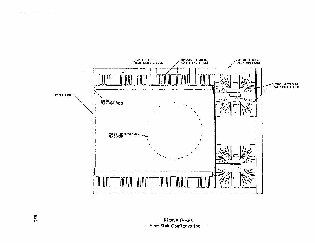


This section of the report corresponds to points four and five (a) ofthe Plan outlined in the objectives of this report.
v Conclusion
A) Evaluating of Final Package
The conclusion of the results of a project such as this must ultimatelyrelate to the objectives set down at the onset of a project. Not all ofthe objectives were proven explicitly, due to the limited time remaininfor testing. However, results from the tests that were made can beextrapolated into other areas.
1. Welding Performance
The basic module could supply 100a AC at 7000 Hz. This fallsshort of the 250 amp AC goal. Test indicated, however, that7000 Hz welding may be difficult, and have adverse effects onthe weld and welder. However, AC welding at 60 Hz may beestablished from 7000 Hz using electronic techniques, thuseliminating transmission and welding difficulties.
The basic module could supply 250a DC and have the capabilityof being paralleled with other modules to provide up to 1000a DC.Only one unit was fabricated, thus parallel capability could notbe established explicitly; however, the nature of the output cir-cuitry is such that parallel capability (DC) may be conducted,though it is not proven explicitly.
Welding operations of downhand stick Mig and Tig welding wereperformed. Due to lack of time, other processes mentioned inthe objectives were not tested explicitly, but there is reason toassume performance in the other categories.
From a welding standpoint then, the final unit did fulfill aportion of the desired objectives.
2. Electronic arid Maintainability Performance
The unit operated from 440 VAC 60 Hz line power and was capableof compensating for fluctuations in primary line voltage. A closedloop feedback system was utilized for this function.
Visual failure signals were not incorporated into the final unitnor were remote control capabilities. These functions are, froma design point of view, relatively easy to incorporate into a system
65

v A) 2. Electronic and Maintainability Performance (Continued)
B)
The basic module final weight was 98 lbs. and rectangularlyshaped for easy handling. Duty cycle was less than 100%.The basic module was free from vents and openings and cooledby convection only. Water cooling and forced air cooling werenot used.
Power supply components consisted of plug-in modules in thecontrol system portion. The final unit was of prototype natureand thus not capable of withstanding rough handling. Thiscapability, however, can be incorporated into production units.There is nothing inherent in "electronic” components that makethem necessarily fragile.
From an economic and reliability point of view, the electronicdesign utilizing transistors is not the optimum design. It isfelt that SCR’s provide a cheaper, more reliable means ofswitching than transistors, providing they can be efficientlycontrolled at the frequencies needed for this design concept.
Recommendations for Future Study
Since the unit that the Celesco Engineering staff produced as a result ofa project initiated by the Marad Commission demonstrates feasibilitymore so than producibility, further work is necessary to reduce thenow proven concept to practice. The following recommendations forfuture study can be made:
1.
2.
3.
4.
Reduce the input line voltage to 220V. The 440 volt line pushedstate-of-the-art semiconductor ratings. By reducing the inputrequirements by half, reliability is considerably improved.Since the concept affords high efficiency at power factors closeto 1, a 300 amp lighfweight supply would draw about the samecurrent from a 220V, 3 phase line. Thus the voltage on powercables could be reduced, thus increasing safety without increasingwire size.
As mentioned, SCR’s should be investigated in the light ofwhat has been learned by the transistor investigation.
SCR's and electronic techniques should be investigated to converthigh frequency of conversion back to 60 Hz for AC welding.
An interest has been expressed in a low current (to 150a) 120 VAC60 Hz single phase "mini" supply. This should also be investigated.
![I'lFIITHBIR UNIVERSITYexampapers.nust.na/greenstone3/sites/localsite/collect... · 2020-04-08 · 4.1.1 Using theresults from output above, calculate the regression estimate. [3]](https://img.pdfslide.us/doc/110x75/5f34c61c11c3d434fa1d4dc1/ilfiithbir-2020-04-08-411-using-theresults-from-output-above-calculate-the.jpg)


![RESEARCH OpenAccess Improvingbiomedicalinformation ... · (Porter)stemmingmethods[11,15,16],but[4]theresults are largely similar. In terms of MAP, Porter is slightly better [4]. Baselineexperiment(getinitialqueryresults)](https://img.pdfslide.us/doc/110x75/5fd11990114f905cad3ba8cc/research-openaccess-improvingbiomedicalinformation-porterstemmingmethods111516but4theresults.jpg)


![LieART - A Mathematica Application for Lie Algebras and ... · productsandbranchingrules. Thesetablesfollow[7]inselectionandpresentationstyle,butextendmostof theresults. Weplantomaintainandfurtherextendourtables,whichcanbeuseddirectlyaslookuptables](https://img.pdfslide.us/doc/110x75/5b469eb97f8b9a3a058ba143/lieart-a-mathematica-application-for-lie-algebras-and-productsandbranchingrules.jpg)