Embed Size (px)
Citation preview
Chapter 2 – The Power Wall and Multicore ComputersChapter OverviewThe material in this chapter is considered a continuation of the previous chapter, which covers the history of computing to about 1995 or so. This chapter presents a design problem that first appeared about 2002 to 2005. This problem is related to heat dissipation from the CPU; when it gets too hot, it malfunctions. This material is placed in a separate chapter on the chance that an instructor wants to assign it without requiring the earlier history.
Chapter AssumptionsThe reader is assumed to have a basic understanding of direct–current electronics, more specifically the relationship of power and current to electrical power dissipated. Most of this material is based on Ohm’s law. The reader is also expected to understand the concept of area density; if one million transistors are placed on a chip that has area of one square millimeter, then the transistor density is one million per square centimeter.
The reader is also assumed to have a grasp of the basic law of physics that any power consumed by an electronic circuit is ultimately emitted as heat. If we say that a CPU consumes 50 watts of electrical power, we then say that it emits 50 watts of heat. We do note that heat is usually measured in units different from those used to measure electrical power, but the two are interchangeable through well–established conversion equations.
Two of the more significant (but not only) factors on total heat radiated by a chip are the voltage and transistor areal density. One version of Ohm’s law states that the heat dissipated by a transistor varies as the square of the voltage; this is important. As the important measure is heat radiated per unit area, more densely packed transistors will emit more heat per unit area than less densely packed.
Introduction to the TopicIt should be no news to anyone that electronic computers have progressed impressively in power since they were first introduced about 1950. One of the causes of this progress has been the constant innovation in technology with which to implement the digital circuits. The last phase of this progress, beginning about 1972, was the introduction of single–chip CPUs. These were first fabricated with LSI (Large Scale Integrated) circuit technology, and then with VLSI (Very Large Scale Integrated) circuitry. As we trace the later development of CPUs, beginning about 1988, we see a phenomenal increase in the number of transistors placed on CPU chip, without a corresponding increase in chip area.
There are a number of factors contributing to the increased computing power of modern CPU chips. All are directly or indirectly due to the increased transistor density found on those chips. Remember that the CPU contains a number of standard circuit elements, each of which has a fixed number of transistors. Thus, an increase in the number of transistors on a chip directly translates to an increase in either the number of logic circuits on the chip, or the amount of cache memory on a chip, or both. Specific benefits of this increase include:
1. Decreased transmission path lengths, allowing an increase in clock frequency.2. The possibility of incorporating more advanced execution units on the CPU. For
example, a pipelined CPU is much faster, but requires considerable circuitry.3. The use of on–chip caches, which are considerably faster than either off–chip
caches or primary DRAM.
Page 69 CPSC 5155 Last Revised July 1, 2011Copyright © by Edward L. Bosworth, Ph.D. All rights reserved.
Before discussing transistor counts and transistor densities, your author (because he has a strange sense of humor) wants to introduce a off–beat measure of area that can easily be applied to measuring CPU chips. This unit is the “nanoacre”. The acre is a unit of measure normally used in land surveys. One acre equals approximately 4,050 square meters, or 4.05109 square millimeters. Thus, one nanoacre equals 4.05 mm2, a square about 2.02 millimeters (0.08 inches) on a side. The die for the Intel Core Extreme x6800 chip has area of about 143 mm2, equal to approximately 35 nanoacres. Incidentally, the size of a typical office cubicle is about 1 milliacre. So much for geek humor.
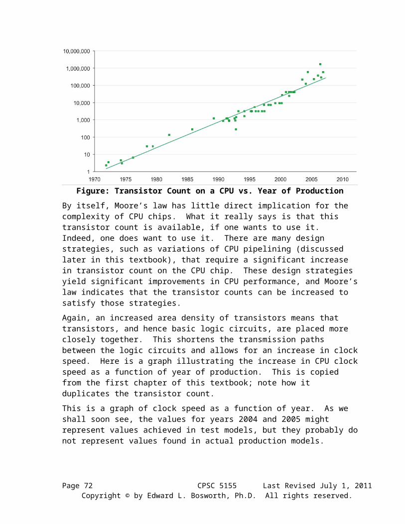
For VLSI implementations of CPU chips, the increase in transistor count has followed what is commonly called “Moore’s Law”. Named for Gordon Moore, the co–founder of Intel Corporation, this is an observation on the number of transistors found on a fixed–sized integrated circuit. While not technically in the form of a law, the statement is so named because the terms “Moore’s Observation”, “Moore’s Conjecture” and “Moore’s Lucky Guess” lack the pizazz that we expect for the names of popular statements.
In a previous chapter, we have shown a graph of transistor count vs. year that represents one statement of Moore’s Law. Here is a more recent graph from a 2009 paper [R79]. The vertical axis (logarithmic scale) represents the transistor count on a typical VLSI circuit.
Figure: Transistor Count on a CPU vs. Year of Production
By itself, Moore’s law has little direct implication for the complexity of CPU chips. What it really says is that this transistor count is available, if one wants to use it. Indeed, one does want to use it. There are many design strategies, such as variations of CPU pipelining (discussed later in this textbook), that require a significant increase in transistor count on the CPU chip. These design strategies yield significant improvements in CPU performance, and Moore’s law indicates that the transistor counts can be increased to satisfy those strategies.
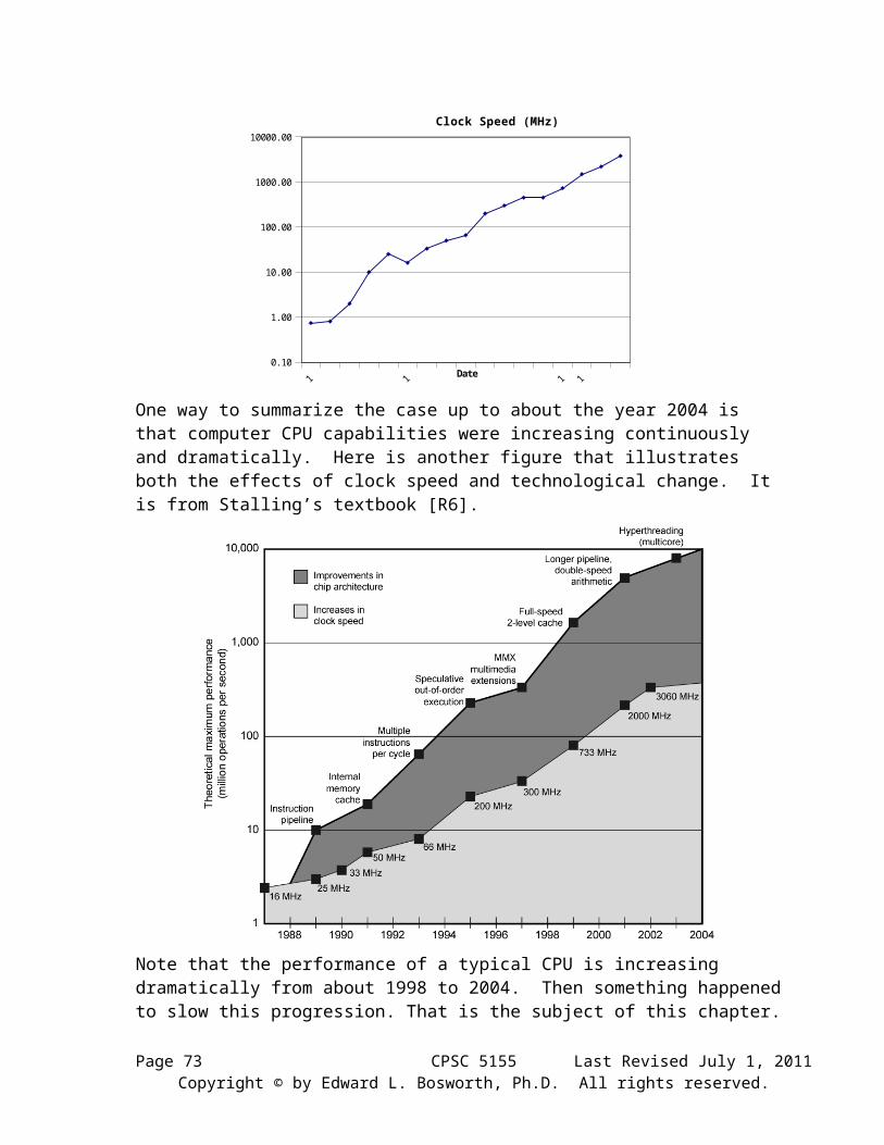
Again, an increased area density of transistors means that transistors, and hence basic logic circuits, are placed more closely together. This shortens the transmission paths between the logic circuits and allows for an increase in clock speed. Here is a graph illustrating the increase in CPU clock speed as a function of year of production. This is copied from the first chapter of this textbook; note how it duplicates the transistor count.
Page 70 CPSC 5155 Last Revised July 1, 2011Copyright © by Edward L. Bosworth, Ph.D. All rights reserved.
This is a graph of clock speed as a function of year. As we shall soon see, the values for years 2004 and 2005 might represent values achieved in test models, but they probably do not represent values found in actual production models.
0.10
1.00
10.00
100.00
1000.00
10000.00
Clock Speed (MHz)
Date
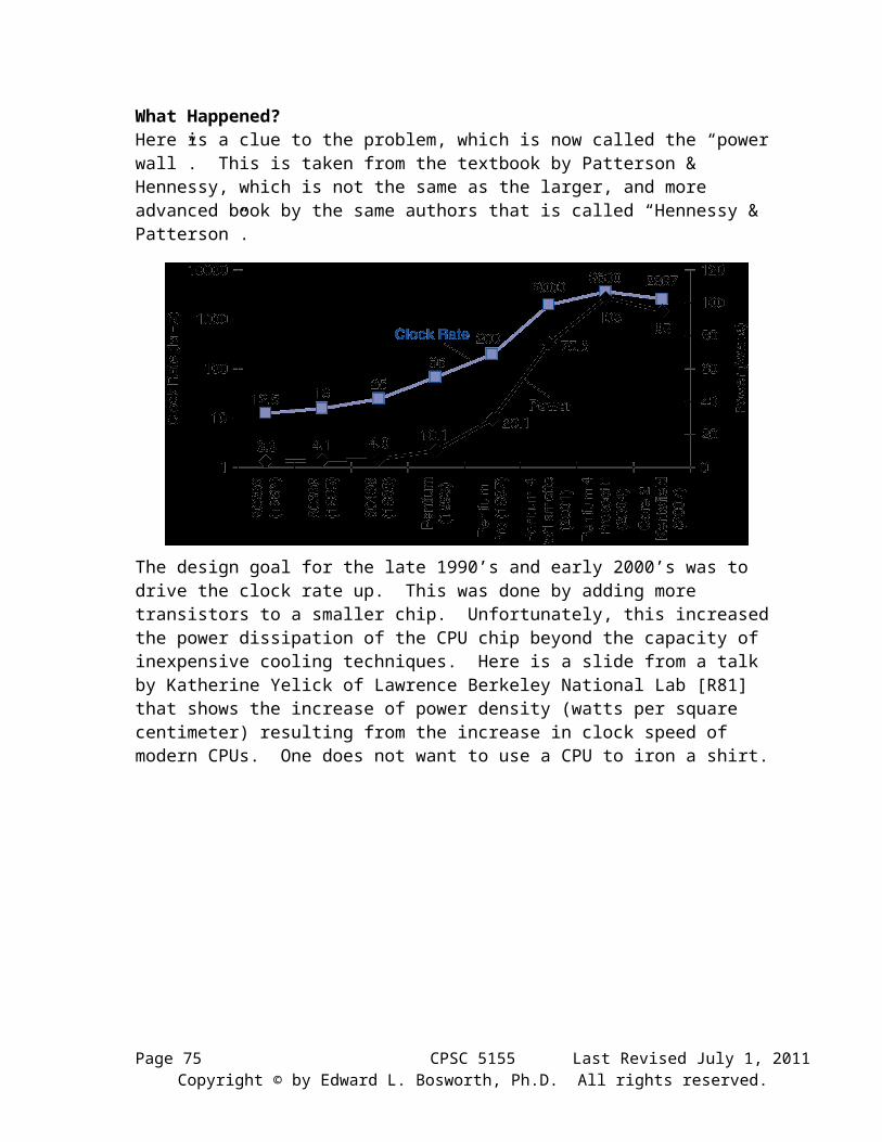
One way to summarize the case up to about the year 2004 is that computer CPU capabilities were increasing continuously and dramatically. Here is another figure that illustrates both the effects of clock speed and technological change. It is from Stalling’s textbook [R6].
Note that the performance of a typical CPU is increasing dramatically from about 1998 to 2004. Then something happened to slow this progression. That is the subject of this chapter.
Page 71 CPSC 5155 Last Revised July 1, 2011Copyright © by Edward L. Bosworth, Ph.D. All rights reserved.
What Happened?Here is a clue to the problem, which is now called the “power wall”. This is taken from the textbook by Patterson & Hennessy, which is not the same as the larger, and more advanced book by the same authors that is called “Hennessy & Patterson”.
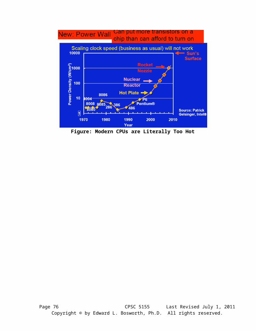
The design goal for the late 1990’s and early 2000’s was to drive the clock rate up. This was done by adding more transistors to a smaller chip. Unfortunately, this increased the power dissipation of the CPU chip beyond the capacity of inexpensive cooling techniques. Here is a slide from a talk by Katherine Yelick of Lawrence Berkeley National Lab [R81] that shows the increase of power density (watts per square centimeter) resulting from the increase in clock speed of modern CPUs. One does not want to use a CPU to iron a shirt.
Figure: Modern CPUs are Literally Too Hot
Page 72 CPSC 5155 Last Revised July 1, 2011Copyright © by Edward L. Bosworth, Ph.D. All rights reserved.
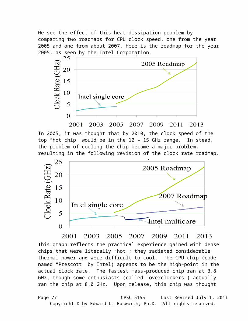
We see the effect of this heat dissipation problem by comparing two roadmaps for CPU clock speed, one from the year 2005 and one from about 2007. Here is the roadmap for the year 2005, as seen by the Intel Corporation.
In 2005, it was thought that by 2010, the clock speed of the top “hot chip” would be in the 12 – 15 GHz range. In stead, the problem of cooling the chip became a major problem, resulting in the following revision of the clock rate roadmap.
This graph reflects the practical experience gained with dense chips that were literally “hot”; they radiated considerable thermal power and were difficult to cool. The CPU chip (code named “Prescott” by Intel) appears to be the high–point in the actual clock rate. The fastest mass–produced chip ran at 3.8 GHz, though some enthusiasts (called “overclockers”) actually ran the chip at 8.0 GHz. Upon release, this chip was thought to generate about 40% more heat per clock cycle that earlier variants. This gave rise to the name “PresHot”.
The Prescott was an early model in the architecture that Intel called “NetBurst”, which was intended to be scaled up eventually to ten gigahertz. The heat problems could never be handled, and Intel abandoned the architecture. The Prescott idled at 50 degrees Celsius (122 degrees Fahrenheit). Even equipped with the massive Akasa King Copper heat sink , the system reached 77 Celsius (171 F) when operating at 3.8 GHz under full load and shut itself down.
Page 73 CPSC 5155 Last Revised July 1, 2011Copyright © by Edward L. Bosworth, Ph.D. All rights reserved.

Here are pictures of two commercial heat sinks for Pentium–class CPUs. Note how large they are. Most users would not care to have such equipment on their computers.
Figure: The Akasa Copper Heat Sink TheMugen 2 Cooler
Another way to handle the heat problem would have been to introduce liquid cooling. Most variants of this scheme use water cooling, though the Cray–2 used the chemical Flourinert, originally developed for medical use. The problem with liquid cooling is that most users do not want to purchase the additional equipment required.
The IBM z/10 mainframe computer is one that uses water cooling. This is a multiprocessor system based on the IBM Power 6 CPU, running at 4.67 GHz, more than 50% faster than the Intel Prescott. It is reported that lab prototypes have been run at 6 GHz.
Here is the water cooling system for the z/10. It is massive.
The copper tubing feeds cold water to cooling units in direct contact with the CPU chips. Each CPU chip is laid out not to have “hot spots”. One of the IBM laboratories in Germany has used this cooling water (warmed by the computer) to heat buildings in winter.
So, we have a problem. It can be solved either by the use of massive cooling systems (not acceptable to most users of desktop computers), or come up with another design. Intel chose to adopt a strategy called “multicore”, also called “chip multiprocessor” or “CMP”.
The solution adopted by Intel Corporation was to attack the problem at its source; reduce the power consumption of the CPU while maintaining or increasing performance. As early as October 2009 [R82], Intel was speaking of two time periods in the development of VLSI chips: the “traditional–scaling” period and the “post traditional–scaling” period. The dividing line between the two was set some time in the year 2003.
Page 74 CPSC 5155 Last Revised July 1, 2011Copyright © by Edward L. Bosworth, Ph.D. All rights reserved.
At this point, Intel and other companies are attempting to address two related problems.1. How to get increased performance out of a CPU without overheating it.2. Addressing the concerns of large data centers that may have thousands of processors
and want to lower their bills for electrical power and cooling.
One obvious example of the second problem can be seen in organizations that might be called “scientific data centers”. These are centers that run a few large supercomputers, each of which is fabricated from thousands of processors that are networked together. One good example of such a supercomputer is the Cray–XK6.
The Cray–XK6 [R83] can be configured with up to 500,000 cooperating processors, organized into “compute nodes” that combine AMD’s 16–core Opteron 6200 processors and NVIDIA’s Tesla X2090 GPU (Graphical Processing Unit), used as a vector processor. Typically, the computer is organized into a number of cabinets, each of which holds up to 96 compute nodes; the picture on the web site shows a 16–cabinet configuration.
Each cabinet requires about 50 kilowatts of power, with additional power required to cool the computer room. Remember that each cabinet produces about fifty kilowatts of heat, which requires power–consuming air conditioning to remove. Any reduction in the power consumption of a compute node would yield immediate benefits.
Here is the characterization of the power problem given by Intel in a white paper entitled “Solving Power and Cooling Challenges for High Performance” [R84], published in June 2006. “It takes a comprehensive strategy to scale high performance computing (HPC) capabilities, while simultaneously containing power and cooling costs.”
The executive summary of this presentation is worth quoting at some length.
“Relief has arrived for organizations that need to pack more computing capacity into existing high performance computing (HPC) facilities, while simultaneously reducing power and cooling costs. For some time, Intel has been focused on helping IT managers address these issues, by driving new levels of energy-efficiency through silicon, processor, platform and software innovation. The results of these efforts are clearly evident in the new Dual-Core Intel® Xeon® processor 5100 series (code-name Woodcrest) and the upcoming Dual-Core Intel® Itanium® 2 processor 9000 series (code-name Montecito), which dramatically increase performance and energy-efficiency compared to previous generations.”
“These and other recent innovations are major steps toward increasing density, pure performance, price/performance and energy-efficiency for HPC solutions, but they are only the beginning. Intel researchers continue to push the limits of transistor density in next-generation process technologies, while simultaneously driving down power consumption. Intel is also delivering software tools, training and support that help developers optimize their software for multi-core processors and 64-bit computing. These are essential efforts, since optimized software can substantially boost performance and system utilization, while contributing to the containment or even reduction of power consumption.” [R84]
Page 75 CPSC 5155 Last Revised July 1, 2011Copyright © by Edward L. Bosworth, Ph.D. All rights reserved.
Recent experience has shown that one way to handle the power problem of a highly pipelined CPU with a high clock frequency is to replace this single large processor by a number of smaller and simpler processors with lower clock frequency. In effect, this places multiple CPUs on a single chip; though the terminology is to refer to multiple cores on a single CPU chip. The decreased complexity of the instruction pipeline in each core yields a reduction in the transistor count (hence transistor density) at little cost in performance for the multiple cores considered as a single CPU. As a bonus, one gets more chip area onto which a larger cache memory can be placed. Increasing the size of an on–chip cache memory is one of the most cost–effective and power–effective ways to boost performance.
In a 2006 white paper, Geoff Koch described Intel’s rationale for multicore processing.
“Explained most simply, multi–core processor architecture entails silicon design engineers placing two or more execution cores – or computational engines – within a single processor. This multi–core processor plugs directly into a single processor socket, but the operating system perceives each of its execution cores as a discrete logical processor with associated execution resources.” [R85]
“Multi–core chips do more work per clock cycle, and thus can be designed to operate at lower frequencies than their single–core counterparts. Since power consumption goes up proportionally with frequency, multi–core architecture gives engineers the means to address the problem of runaway power and cooling requirements.” [R85]
A bit later, Koch notes the following.
“With Intel Core microarchitecture, each core is equipped with a nearly complete set of hardware resources, including cache memory, floating point and integer units, etc. One programming thread can utilize all these resources while another thread can use all the hardware resources on another core.” [R85]
Anyone familiar with the use of MS–Windows on a modern computer will recall that there are always multiple processes under execution at any one time. These processes can be executed one at a time on a single CPU or more efficiently on a multicore CPU. In other words, the typical MS–Windows work load favors use of multicore designs.
Here is a picture of the core die and a diagram of one of the more recent Intel multicore offerings, the quad–core CPU called Core i7. Each execution core has its own split L1 cache as well as a level–2 cache. The four cores share a large level–3 cache.
Page 76 CPSC 5155 Last Revised July 1, 2011Copyright © by Edward L. Bosworth, Ph.D. All rights reserved.
One of the key goals, evident in a number of publications [R79, R84] is to increase the system performance per watt of power used. The following is a figure from the Intel White Paper [R84] showing the increase in performance on several standard benchmarks achieved by the new design, called “Woodcrest”.
As of the year 2010, Intel has announced a number of multicore offerings. Most of those available had either four or eight cores per chip. There is a reports, dated in 2009, found on Wikipedia [R86] of Intel releasing a single–chip 48–core CPU “for software and circuit research in cloud computing”. The Wikipedia reference is the link [R87]. There is also a reference in the Wikipedia article to a single–chip 80–core CPU prototype [R88]. The author of this textbook has not been able to verify either claim, using only material from an Intel Corporation web site. However, each claim is probably true.
Later in this textbook, we shall discuss issues of parallel computing in general. At that time, we shall introduce the term “manycore computer”, as distinct from “multicore computer”. The distinction originates from the development of the NVIDIA GPU (Graphical Processor Unit) which could feature 768 execution cores, as opposed to the 8 cores found on multicore computers of the time. There may be a dividing line of core count between the two design philosophies, but it has yet to be defined. It may never be defined. Time will tell.
Page 77 CPSC 5155 Last Revised July 1, 2011Copyright © by Edward L. Bosworth, Ph.D. All rights reserved.