Embed Size (px)
Citation preview
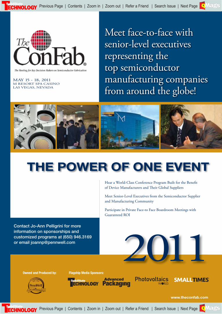
Meet face-to-face with senior-level executives representing the top semiconductor manufacturing companies from around the globe!
MAY 15 - 18, 2011M RESORT SPA CASINOLAS VEGAS, NEVADA
2011www.theconfab.com
Owned and Produced by: Flagship Media Sponsors:
THE POWER OF ONE EVENT
Hear a World-Class Conference Program Built for the Benefi t
of Device Manufacturers and Th eir Global Suppliers
Meet Senior-Level Executives from the Semiconductor Supplier
and Manufacturing Community
Participate in Private Face-to Face Boardroom Meetings with
Guaranteed ROI
Contact Jo-Ann Pelligrini for more
information on sponsorships and
customized programs at (650) 946.3169
or email [email protected]
Previous Page | Contents | Zoom in | Zoom out | Refer a Friend | Search Issue | Next PageDC B
A
M SaGEF
Previous Page | Contents | Zoom in | Zoom out | Refer a Friend | Search Issue | Next PageDC B
A
M SaGEF

The lifesaving microchip never failed thanks to a powerful
protective silicone coating created by NuSil.
It’s part of our extensive line of low-outgassing materials
designed and tested to perform with low contamination
in harsh environments and extreme thermal conditions.
At NuSil, our scientists are dedicated to helping innovators
innovate. Whether your needs are for large batches or
small, you can depend on the leader in silicone solutions
with nearly 30 years of electronics experience.
We want every product story to have a happy ending.
What? When? Where? If it’s NuSil, it’s no problem.
Lost puppy.
Implanted microchip.
Welcome home, Lucky.
NuSil Technology.
What’s your challenge? www.nusil.com/ap USA +1-805-684-8780Europe +33 (0) 4 92 96 93 31©2010 NuSil Technology LLC. All rights reserved. AP0410-E
Previous Page | Contents | Zoom in | Zoom out | Refer a Friend | Search Issue | Next PageDC B
A
M SaGEF
Previous Page | Contents | Zoom in | Zoom out | Refer a Friend | Search Issue | Next PageDC B
A
M SaGEF

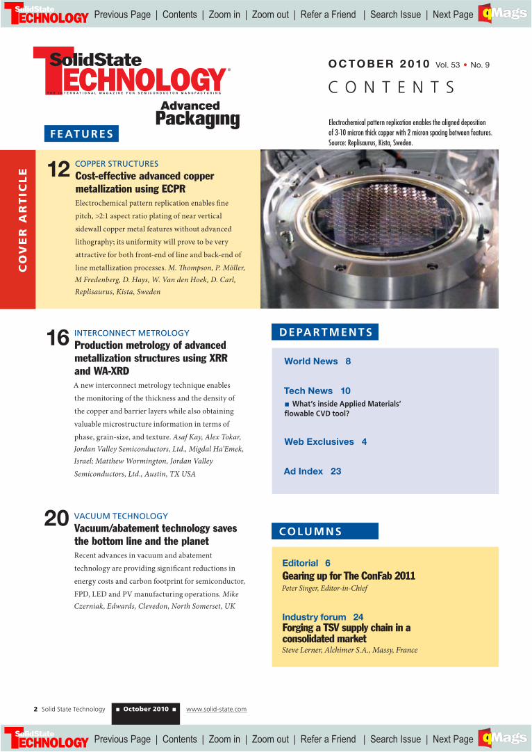
OCTOBER 2010
www.solid-state.com
Cost-Effective Copper Metallization p. 12
■ Production Metrology of Advanced Copper Structures p. 16
■ “Green” Vacuum and Abatement Technology p. 20
■ Forging a TSV Supply Chain p. 22
Contents | Zoom In | Zoom Out Search Issue | Next PageFor navigation instructions please click here
Contents | Zoom In | Zoom Out Search Issue | Next PageFor navigation instructions please click here
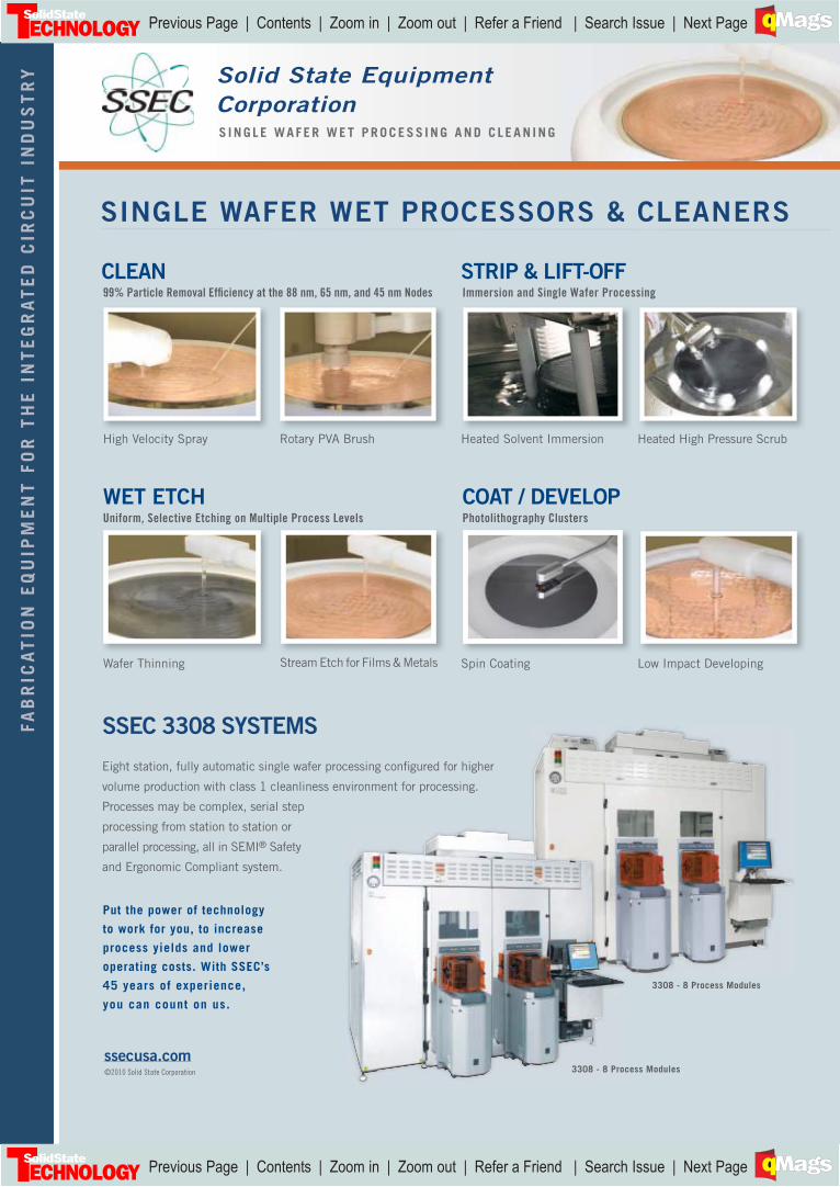
CLEAN99% Particle Removal Efficiency at the 88 nm, 65 nm, and 45 nm Nodes
STRIP & LIFT-OFFImmersion and Single Wafer Processing
High Velocity Spray Rotary PVA Brush Heated Solvent Immersion Heated High Pressure Scrub
WET ETCHUniform, Selective Etching on Multiple Process Levels
COAT / DEVELOPPhotolithography Clusters
Stream Etch for Films & MetalsWafer Thinning Low Impact DevelopingSpin Coating
SINGLE WAFER WET PROCESSORS & CLEANERS
FAB
RIC
AT
ION
EQ
UIP
ME
NT
FO
R T
HE
IN
TE
GR
AT
ED
CIR
CU
IT I
ND
US
TR
Y
ssecusa.com©2010 Solid State Corporation
Solid State Equipment
CorporationS I N G L E WA F E R W E T P R O C E S S I N G A N D C L E A N I N G
SSEC 3308 SYSTEMS
3308 - 8 Process Modules
Eight station, fully automatic single wafer processing configured for higher
volume production with class 1 cleanliness environment for processing.
Processes may be complex, serial step
processing from station to station or
parallel processing, all in SEMI® Safety
and Ergonomic Compliant system.
Put the power of technology
to work for you, to increase
process yields and lower
operating costs. With SSEC’s
45 years of experience,
you can count on us.
3308 - 8 Process Modules
Previous Page | Contents | Zoom in | Zoom out | Refer a Friend | Search Issue | Next PageDC B
A
M SaGEF
Previous Page | Contents | Zoom in | Zoom out | Refer a Friend | Search Issue | Next PageDC B
A
M SaGEF

chnology.com
���������� ������� ��������������� ����������������
�����������
�������
������� ����������
■���������������� ��������������������������� ����������������������� �������������������������
■������������������������������ ��� ����������������������������� ����
■��� ���!"���#������� ����� #�$��������������
■���%��������������� ���������������������� �������������&���&�&�&����&���
■�����' ����������������������������������#�&����&����������#����(�� #� ��� )
■���'�� ����!'�'*+�������������#�����������������,��#�-��&���.���������
���������� ����������������&�� ��#/
����������� ���������������������� ��������
����������������������������
����������������������������������������������������������������������������������������������������������������������������������������������������������������������������������������������������������������������������������������������������������������������������������������������������������������������������������������������������������������������������������������������
Previous Page | Contents | Zoom in | Zoom out | Refer a Friend | Search Issue | Next PageDC B
A
M SaGEF
Previous Page | Contents | Zoom in | Zoom out | Refer a Friend | Search Issue | Next PageDC B
A
M SaGEF
_________________
FE ATU RES
C O N T E N T S
O C TO B E R 2 010 Vol. 53 • No. 9
2 Solid State Technology ■ October 2010 ■ www.solid-state.com
DEPA R TMEN T S
COLUMNS
INTERCONNECT METROLOGY
Production metrology of advanced
metallization structures using XRR
and WA-XRD
A new interconnect metrology technique enables
the monitoring of the thickness and the density of
the copper and barrier layers while also obtaining
valuable microstructure information in terms of
phase, grain-size, and texture. Asaf Kay, Alex Tokar,
Jordan Valley Semiconductors, Ltd., Migdal Ha’Emek,
Israel; Matthew Wormington, Jordan Valley
Semiconductors, Ltd., Austin, TX USA
VACUUM TECHNOLOGY
Vacuum/abatement technology saves
the bottom line and the planet
Recent advances in vacuum and abatement
technology are providing signifi cant reductions in
energy costs and carbon footprint for semiconductor,
FPD, LED and PV manufacturing operations. Mike
Czerniak, Edwards, Clevedon, North Somerset, UK
16
20
Electrochemical pattern replication enables the aligned deposition of 3-10 micron thick copper with 2 micron spacing between features. Source: Replisaurus, Kista, Sweden.
COPPER STRUCTURES
Cost-effective advanced copper
metallization using ECPR
Electrochemical pattern replication enables fi ne
pitch, >2:1 aspect ratio plating of near vertical
sidewall copper metal features without advanced
lithography; its uniformity will prove to be very
attractive for both front-end of line and back-end of
line metallization processes. M. Th ompson, P. Möller,
M Fredenberg, D. Hays, W. Van den Hoek, D. Carl,
Replisaurus, Kista, Sweden
CO
VE
R A
RT
IC
LE 12
World News 8
Tech News 10
■ What’s inside Applied Materials’
flowable CVD tool?
Web Exclusives 4
Ad Index 23
Editorial 6
Gearing up for The ConFab 2011Peter Singer, Editor-in-Chief
Industry forum 24
Forging a TSV supply chain in a consolidated marketSteve Lerner, Alchimer S.A., Massy, France
Previous Page | Contents | Zoom in | Zoom out | Refer a Friend | Search Issue | Next PageDC B
A
M SaGEF
Previous Page | Contents | Zoom in | Zoom out | Refer a Friend | Search Issue | Next PageDC B
A
M SaGEF
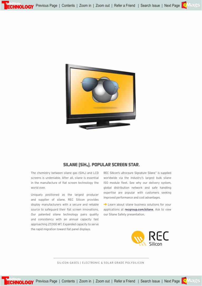
The chemistry between silane gas (SiH4) and LCD
screens is undeniable. After all, silane is essential
in the manufacture of flat screen technology the
world over.
Uniquely positioned as the largest producer
and supplier of silane, REC Silicon provides
display manufacturers with a secure and reliable
source to safeguard their flat screen innovations.
Our patented silane technology pairs quality
and consistency with an annual capacity fast
approaching 27,000 MT. Expanded capacity to serve
the rapid migration toward flat panel displays.
SILANE (SiH4). POPULAR SCREEN STAR.
REC Silicon’s ultra-pure Signature Silane™ is supplied
worldwide via the industry’s largest bulk silane
ISO module fleet. See why our delivery system,
global distribution network and safe handling
expertise are popular with customers seeking
improved performance and cost advantages.
Learn about silane business solutions for your
applications at recgroup.com/silane. Ask to view
our Silane Safety presentation.
SILICON GASES | ELECTRONIC & SOLAR GRADE POLYSILICON
Previous Page | Contents | Zoom in | Zoom out | Refer a Friend | Search Issue | Next PageDC B
A
M SaGEF
Previous Page | Contents | Zoom in | Zoom out | Refer a Friend | Search Issue | Next PageDC B
A
M SaGEF
4 Solid State Technology ■ October 2010 ■ www.solid-state.com
Diane Lieberman, Group Publisher,Ph: 603/891-9441, [email protected]
Peter Singer, Editor-in-Chief, Ph: 603/891-9217, [email protected]
Meredith Courtemanche, Editor, Digital MediaPh: 603/891-9176, [email protected]
Robert C. Haavind, Editor-at-Large, Ph: 603/891-9453, [email protected]
Debra Vogler, Senior Technical Editor, Ph: 408/774-9283, [email protected]
James Montgomery, News Editor, Ph: 603/891-9109, [email protected]
Katherine Derbyshire, Contributing Technical Editor
Selma Uslaner, Director of Industry Relations
Rachael Caron, Marketing Manager
Cindy Chamberlin, Presentation Editor
Katie Noftsger, Production Manager
Dan Rodd, Illustrator
Michelle McKeon, Audience Development Manager
Marcella Hanson, Ad Traffi c Manager
EDITORIAL ADVISORY BOARD
John O. Borland, J.O.B. Technologies
Jeffrey C. Demmin, Tessera Technologies Inc.
Michael A. Fury, The Techcet Group, LLC
Rajarao Jammy, SEMATECH
William Kroll, Matheson Tri-Gas
Ernest Levine, Albany NanoTech
Lars Liebmann, IBM Corp.
Dipu Pramanik, Cadence Design Systems Inc.
Griff Resor, Resor Associates
Linton Salmon, TI
A.C. Tobey, ACT International
EDITORIAL OFFICES
PennWell Corporation, Solid State Technology
98 Spit Brook Road LL-1,
Nashua, NH 03062-5737;
Tel: 603/891-0123; Fax: 603/891-0597;
www.solid-state.com
CORPORATE OFFICERS
1421 SOUTH SHERIDAN RD., TULSA, OK 74112
TEL: 918/835-3161
Frank T. Lauinger, Chairman
Robert F. Biolchini, President and CEO
Mark Wilmoth, Chief Financial Offi cer
TECHNOLOGY GROUP
Christine A. Shaw, Senior Vice President and Publishing Director
Gloria Adams, Senior VP, Audience Development
For subscription inquiries:Tel: (847) 559-7500; Fax: (847) 291-4816;Customer Service e-mail: [email protected];
Subscribe: www.sst-subscribe.com
Solid State Technology ONLINE
Web Exclusives
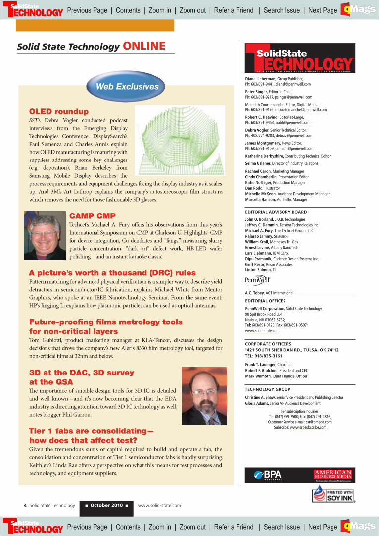
OLED roundupSST’s Debra Vogler conducted podcast
interviews from the Emerging Display
Technologies Conference. DisplaySearch’s
Paul Semenza and Charles Annis explain
how OLED manufacturing is maturing with
suppliers addressing some key challenges
(e.g. deposition). Brian Berkeley from
Samsung Mobile Display describes the
process requirements and equipment challenges facing the display industry as it scales
up. And 3M’s Art Lathrop explains the company’s autostereoscopic fi lm structure,
which removes the need for those fashionable 3D glasses.
CAMP CMPTechcet’s Michael A. Fury off ers his observations from this year’s
International Symposium on CMP at Clarkson U. Highlights: CMP
for device integration, Cu dendrites and “fangs,” measuring slurry
particle concentration, “dark art” defect work, HB-LED wafer
polishing—and an instant karaoke classic.
A picture’s worth a thousand (DRC) rulesPattern matching for advanced physical verifi cation is a simpler way to describe yield
detractors in semiconductor/IC fabrication, explains Michael White from Mentor
Graphics, who spoke at an IEEE Nanotechnology Seminar. From the same event:
HP’s Jingjing Li explains how plasmonic particles can be used as optical antennas.
Future-proofi ng fi lms metrology tools
for non-critical layersTom Gubiotti, product marketing manager at KLA-Tencor, discusses the design
decisions that drove the company’s new Aleris 8330 fi lm metrology tool, targeted for
non-critical fi lms at 32nm and below.
3D at the DAC, 3D survey
at the GSATh e importance of suitable design tools for 3D IC is detailed
and well known—and it’s now becoming clear that the EDA
industry is directing attention toward 3D IC technology as well,
notes blogger Phil Garrou.
Tier 1 fabs are consolidating—
how does that affect test?Given the tremendous sums of capital required to build and operate a fab, the
consolidation and concentration of Tier 1 semiconductor fabs is hardly surprising.
Keithley’s Linda Rae off ers a perspective on what this means for test processes and
technology, and equipment suppliers.
Previous Page | Contents | Zoom in | Zoom out | Refer a Friend | Search Issue | Next PageDC B
A
M SaGEF
Previous Page | Contents | Zoom in | Zoom out | Refer a Friend | Search Issue | Next PageDC B
A
M SaGEF

We don’t have a department dedicated to quality. We have a company dedicated to it.
© 2
010
Sw
agel
ok C
ompa
ny
Simulated computer modeling, dimensional testing, and electron scanning
of raw materials – you name it, we’ll go to any lengths to ensure that if it’s
from Swagelok, it’s top quality. Because Quality isn’t just one of our values.
It’s our attitude. It’s the focus of every associate, affecting everything from
our services to our products. And by using the same disciplines, practices,
and technologies through every offi ce in every country, that focus is constant.
We know that quality isn’t just a well-made product, it’s customers served
beyond what they were expecting. To see what that attitude can do for you,
visit swagelok.com/quality.
Previous Page | Contents | Zoom in | Zoom out | Refer a Friend | Search Issue | Next PageDC B
A
M SaGEF
Previous Page | Contents | Zoom in | Zoom out | Refer a Friend | Search Issue | Next PageDC B
A
M SaGEF
E D I T O R I A L
6 Solid State Technology ■ October 2010 ■ www.solid-state.com
As I write this mid-September 2010, the trees are just
starting to turn from green to red and yellow here in
New England and there’s a bit of a chill in the air -- yet
my thoughts have already turned to Spring and fabulous Las
Vegas, Nevada. We are already planning for Th e ConFab
2011, our invitation-only conference and networking event,
to be held May 15-19 at the new M Resort Spa & Casino.
During the last seven years, PennWell and Solid State
Technology have hosted the event, focused squarely on
the economic and technical challenges of semiconductor
manufacturing. As the conference chair, I work with our
advisory board to put together the conference program.
The semiconductor industry went
from having one of the worst years
ever in 2009 to one of the best
years in 2010. But even in this
time of prosperity, I know that
many of us worry about the
future. Is the next downturn
right around the corner? Are
companies adding capacity too
quickly? Is the semiconductor industry
no longer the dynamic growth engine it once
was? What does Asia’s growing dominance mean?
Th en there are the technology hurdles. Pundits are
saying that the high cost of R&D will mean only a handful
of companies will have deep enough pockets to fund the
most advanced technology. Scaling could run out of steam
by 2015 or so and the “next switch” aft er the transistor
has yet to be found. EUV appears to be the lithography
tool of choice, but will it be ready for volume production?
Can 3D integration provide another path to continue with
Moore’s Law?
Answers to these questions are elusive, but these are
exactly the kinds of topics we dig into each year at Th e
ConFab. Earlier this year, we heard from Eli Harrari,
founder and CEO of Sandisk, on the future of the NAND
fl ash business. John Chen, vp of NVIDIA, chaired a panel
where we learned just how keenly interested fabless
companies are in manufacturing capabilities, and how
they are driving manufacturing technology in new direc-
tions. Dr. Norimasa Kishi, director of the Nissan Research
Center, gave us a tantalizing look at the car of the future
and the role automotive electronics will play. Execs from
Texas Instruments gave an in-depth look at their unique
R&D strategy. Other sessions focused on the economic
outlook for the post-recession semiconductor industry,
next generation lithography, collaborative R&D models,
3D integration, and more.
For 2011, we’re aiming even
higher. We plan to sharpen our
focus on the important role
that fabless companies play in driving semiconductor
manufacturing tech. We will explore the opportunities
of high growth markets such as MEMS and LEDs, how
these fi t with traditional semiconductor models, and how
they are driving foundries and equipment and materials
suppliers. Next generation litho is sure to be a hot button,
including EUV, mask technology and multiple e-beam
approaches. 450mm is also sure to be included (particu-
larly since SEMATECH’s Scott Kramer is
now on our advisory board).
Back-end challenges and the
ever-increasing cost contri-
bution to the fi nished part
will also be covered. As one
advisory board member
noted, this part of the supply
chain (OSATs, assembly and test
suppliers) tends to be a somewhat
overlooked/under-served part of our industry.
“Th e days of independent silicon development and package
development are over, as things like CPI (chip packaging
interaction) are heating up and driving collaboration
and/or vertical integration,” he explained.
In these days when social media is all the rage, and online
networking increasingly occupies more of our days, it may
seem extraordinary to host a meeting where people fl y in
from all over the world. But that’s exactly what Th e ConFab
is all about, and it defi nitely is extraordinary!
So how can you participate? Send me your ideas and I’ll
bring them up in our regular discussions with the advisory
board. If you’d like to attend as our guest – no matter where
you are in the world -- point your browser to www.theconfab.
com and check out the attendee qualifi cation form. And, of
course, if you’re interested in joining as a sponsor, please
contact Jo-Ann Pellegrini, Sales Manager, (650) 941-3169,
Regardless of your organization’s place in the semicon-
ductor manfuacturing value chain, you’ll fi nd opportunities
at Th e ConFab to talk business, listen to industry leaders and
confer on matters of importance – but also relax and have
some fun! I hope to see you there. ■
Pete Singer
Editor-in-Chief
Even in this time of
prosperity, I know that many
of us worry about the future. Is the
next downturn right around the corner?
Answers are elusive, but that’s what
we dig into at The ConFab.
Gearing Up for The ConFab 2011
Previous Page | Contents | Zoom in | Zoom out | Refer a Friend | Search Issue | Next PageDC B
A
M SaGEF
Previous Page | Contents | Zoom in | Zoom out | Refer a Friend | Search Issue | Next PageDC B
A
M SaGEF
___

20
200
20
100
20
70
20
50
20
40
20
30
20
25
20
20
1
2
3
4
5
6
7
8
XL R
N O WG I V E S U
T H E N E X TB I G T H I N G I N
N O D E S H R I N K
A T 3 2 N M & B E Y O N D.
XLR 600ix: THE BEST IN CURRENT AND NEXT
GENERATION IMMERSION LITHOGRAPHY.
The XLR 600ix delivers the world’s fi rst light source with selectable power from 60W to 90W.
This new light source benefi ts current and future lithography applications without requiring
additional investments. Superior dose performance, extended lifetime modules and low
operating costs make the XLR 600ix today’s light source of choice. As a company built on
innovation, our advancements continue to minimize your costs and maximize value. Learn more at cymer.com
Previous Page | Contents | Zoom in | Zoom out | Refer a Friend | Search Issue | Next PageDC B
A
M SaGEF
Previous Page | Contents | Zoom in | Zoom out | Refer a Friend | Search Issue | Next PageDC B
A
M SaGEF
0
5
10
15
20
25
30
35
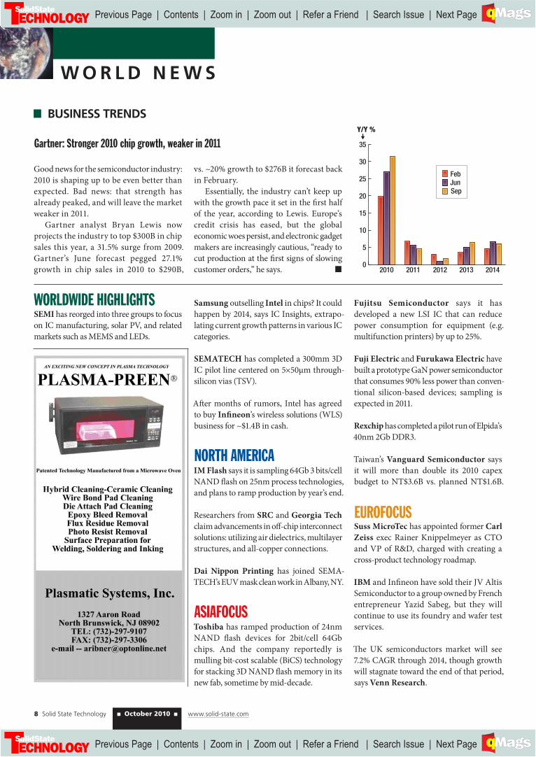
2010 2011 2012
Feb
Jun
Sep
2013 2014
Y/Y %
W O R L D N E W S
8 Solid State Technology ■ October 2010 ■ www.solid-state.com
■ BUSINESS TRENDS
Gartner: Stronger 2010 chip growth, weaker in 2011
Good news for the semiconductor industry:
2010 is shaping up to be even better than
expected. Bad news: that strength has
already peaked, and will leave the market
weaker in 2011.
Gartner analyst Bryan Lewis now
projects the industry to top $300B in chip
sales this year, a 31.5% surge from 2009.
Gartner’s June forecast pegged 27.1%
growth in chip sales in 2010 to $290B,
vs. ~20% growth to $276B it forecast back
in February.
Essentially, the industry can’t keep up
with the growth pace it set in the fi rst half
of the year, according to Lewis. Europe’s
credit crisis has eased, but the global
economic woes persist, and electronic gadget
makers are increasingly cautious, “ready to
cut production at the fi rst signs of slowing
customer orders,” he says. ■
WORLDWIDE HIGHLIGHTSSEMI has reorged into three groups to focus
on IC manufacturing, solar PV, and related
markets such as MEMS and LEDs.
Samsung outselling Intel in chips? It could
happen by 2014, says IC Insights, extrapo-
lating current growth patterns in various IC
categories.
SEMATECH has completed a 300mm 3D
IC pilot line centered on 5×50μm through-
silicon vias (TSV).
Aft er months of rumors, Intel has agreed
to buy Infi neon’s wireless solutions (WLS)
business for ~$1.4B in cash.
NORTH AMERICAIM Flash says it is sampling 64Gb 3 bits/cell
NAND fl ash on 25nm process technologies,
and plans to ramp production by year’s end.
Researchers from SRC and Georgia Tech
claim advancements in off -chip interconnect
solutions: utilizing air dielectrics, multilayer
structures, and all-copper connections.
Dai Nippon Printing has joined SEMA-
TECH’s EUV mask clean work in Albany, NY.
ASIAFOCUSToshiba has ramped production of 24nm
NAND fl ash devices for 2bit/cell 64Gb
chips. And the company reportedly is
mulling bit-cost scalable (BiCS) technology
for stacking 3D NAND fl ash memory in its
new fab, sometime by mid-decade.
Fujitsu Semiconductor says it has
developed a new LSI IC that can reduce
power consumption for equipment (e.g.
multifunction printers) by up to 25%.
Fuji Electric and Furukawa Electric have
built a prototype GaN power semiconductor
that consumes 90% less power than conven-
tional silicon-based devices; sampling is
expected in 2011.
Rexchip has completed a pilot run of Elpida’s
40nm 2Gb DDR3.
Taiwan’s Vanguard Semiconductor says
it will more than double its 2010 capex
budget to NT$3.6B vs. planned NT$1.6B.
EUROFOCUSSuss MicroTec has appointed former Carl
Zeiss exec Rainer Knippelmeyer as CTO
and VP of R&D, charged with creating a
cross-product technology roadmap.
IBM and Infi neon have sold their JV Altis
Semiconductor to a group owned by French
entrepreneur Yazid Sabeg, but they will
continue to use its foundry and wafer test
services.
Th e UK semiconductors market will see
7.2% CAGR through 2014, though growth
will stagnate toward the end of that period,
says Venn Research.
Previous Page | Contents | Zoom in | Zoom out | Refer a Friend | Search Issue | Next PageDC B
A
M SaGEF
Previous Page | Contents | Zoom in | Zoom out | Refer a Friend | Search Issue | Next PageDC B
A
M SaGEF
Previous Page | Contents | Zoom in | Zoom out | Refer a Friend | Search Issue | Next PageDC B
A
M SaGEF
Previous Page | Contents | Zoom in | Zoom out | Refer a Friend | Search Issue | Next PageDC B
A
M SaGEF
___________________________________
Partial fill Full fill
5nmnm5nm5nmm fefeatuatuataa rerer5nm feature
50050000050000nmmnmnm500nm500nm
10 Solid State Technology ■ October 2010 ■ www.solid-state.com
T E C H N O L O G Y N E W S
Chip density is a growing problem. Packing,
and electrically isolating, 400M transistors
on an area the size of a pinhead will
eventually require stacking them verti-
cally—e.g., DRAM memory 4F2 buried
wordline, NAND fl ash “skyscrapers,” and
logic FinFETs. For device architectures,
that means taller and narrower structures,
diff erent types of surfaces and materials that
need to be fi lled under and around (conven-
tional CVD from the bottom/
sides tends to pinch at the top),
and within a required thermal
budget and at a reasonable
complexity and cost.
Applied Materials’ answer:
a liquid fl owable CVD, dubbed
Eterna FCVD, that “fills
anything” with up to 30:1 aspect
ratios. It can fi ll (full and partial)
5nm geometries with “very little
overburden,” and also around
and underneath things like
10nm overhangs, they claim.
The other benefit of the
new technology is elimination
of carbon, which hampers transistor
isolation and causes voltage shift s and
leakage. Current spin-on dielectric (SOD)
technology requires multiple removal steps
to address this, and at anneal temperatures
that become problematic when dealing with
complex device structures. (Ed Korczynski,
former SST senior technical editor and
current blogosphere denizen at Betasights.
net, says AMAT execs confi rm the FCVD
precursor is carbon-free from the start, and
“never sees the plasma.”) FCVD, they claim,
translates into a 50% lower integrated cost
vs. SOD, and up to a day shorter cycle time,
though that will vary by integration scheme
and by fab/customer.
Other details about the tool, gleaned from
AMAT’s presentation and Q&A:
• Th e technology relies on a “unique”
chamber design that allows the precursor
to be introduced and deposited in a
certain way (and is exclusive to AMAT).
Little was revealed about the actual inner
workings of the tool, except that much
of the benefi t is in the hardware. Th ey
acknowledged that the precursor does in
fact enter the chamber as a liquid, broken
up in the top part of the chamber.
• Th ere is no separate licensing fee for
the precursor (>30 precursors were
screened to get the fi nal one), which can
be obtained separately, mostly sourced
from one supplier. Bill McClintock, VP/
GM of the company’s dielectric systems
and CMP unit, added that the precursor
costs “more than 3× less” than what is
used with SOD—reminding that cost
should include not only how much
chemical is used in multiple-step SOD,
but also what is not used (e.g. lost off the
wafer edges and wasted).
• Chipmakers probably need a couple of
these new tools per layer—a minimum
of two layers at 2Xnm node, and as many
as eight or more in forthcoming vertical
structures, according to McClintock.
Th roughput is “moderate,” comparable
to the company’s HARP tools. However,
both he and Randhir Th akur, EVP/GM of
AMAT’s silicon systems group, empha-
sized that throughput is the fl ip side of the
coin from cost, pointing to SOD’s extra
post-treatment steps.
• Filling gaps with a flowable liquid
precursor which reacts during deposition
to form the fi lm isn’t necessarily a
new concept. Trikon, for example,
“did this a few years back with TEOS
and hydrogen peroxide,” Gartner’s
Dean Freeman reminded SST.
Th akur noted earlier eff orts ran into
problems with hardware (how to
bring the precursor into the system)
and precursor quality (e.g. carbon-
free). And removing the carbon ends
up improving electrical performance
and yields. Th akur indicated isolation
and defects that show up in second-
order yield problems in chips, “some
of those electrical issues are not there”
with this fl owable CVD approach.
• Applied claims to have “every major
memory customer” (it counts fi ve) and
one logic fi rm using the tool, with another
logic customer awaiting shipment in 4Q
and a third currently in demos. Th e
company projects a $400M market,
but is banking that customers will fi nd
applications for this FCVD technology
beyond 3D structures in new areas: e.g.,
surface defect masking (where SOD fi lms
would be far too thick), planarizing with
capping fi lms (for small openings at the
top of devices), possibly for some areas
that require an ALD-like fi lm (though
probably not ALD itself, where fi lms are
too thin for this type of tool), or even
gapfi ll for aluminum interconnects. And
AMAT expects that the technology will
fi nd traction at trailing nodes as well—e.g.
qualifi ed at 28nm but then later put into
4Xnm manufacturing, where it could
also simplify gapfi lling and could save
several dollars per wafer. — J.M.
What’s inside Applied Materials’ fl owable CVD tool?
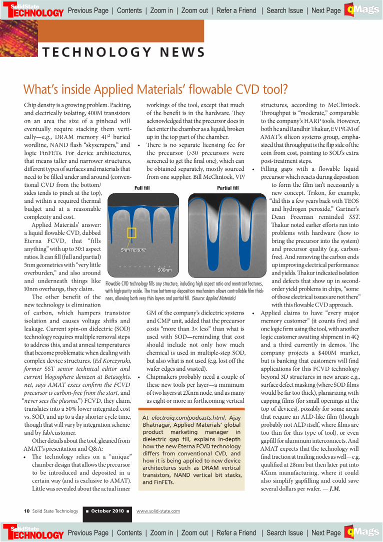
Flowable CVD technology fi lls any structure, including high aspect ratio and reentrant features,
with high-purity oxide. The true bottom-up deposition mechanism allows controllable fi lm thick-
ness, allowing both very thin layers and partial fi ll. (Source: Applied Materials)
At electroiq.com/podcasts.html, Ajay
Bhatnagar, Applied Materials’ global
product marketing manager in
dielectric gap fi ll, explains in-depth
how the new Eterna FCVD technology
differs from conventional CVD, and
how it is being applied to new device
architectures such as DRAM vertical
transistors, NAND vertical bit stacks,
and FinFETs.
Previous Page | Contents | Zoom in | Zoom out | Refer a Friend | Search Issue | Next PageDC B
A
M SaGEF
Previous Page | Contents | Zoom in | Zoom out | Refer a Friend | Search Issue | Next PageDC B
A
M SaGEF
Previous Page | Contents | Zoom in | Zoom out | Refer a Friend | Search Issue | Next PageDC B
A
M SaGEF
Previous Page | Contents | Zoom in | Zoom out | Refer a Friend | Search Issue | Next PageDC B
A
M SaGEF
_____________________
____________________
Master electrode
Electrochemical
micro cells
Electrochemically
transferred metal
ECPR fabricated
metal layer
Electrolyte
Substrate
12 Solid State Technology ■ October 2010 ■ www.solid-state.com
Cost-effective advanced copper metallization using ECPR
COPPER STRUC TURES
A new methodology is required to enable
the cost-effective deposition of thick, tightly-spaced copper structures. In
this review, we introduce the technology of electrochemical pattern rep-
lication (ECPR). ECPR enables the aligned deposition of 3-10μm thick cop-
per with ≥2μm spacing between features. The ECPR process eliminates the
need for copper CMP and photolithography equipment and the related
consumable slurry materials, photolithography resists and solvents. This
ECPR process delivers damascene-like feature control at <50% of the cost
compared to dual damascene targeting analog and RF devices, IPDs, redis-
tribution layers (RDL) and advanced packaging markets.
E XECUTIVE OVE RVIE W
Copper has replaced aluminum as the standard transistor
interconnect metallization material of choice for advanced
logic devices (microprocessors, ASICS) and memories.
Copper is also increasingly utilized in power management
devices, CMOS imagers, and integrated passive devices (IPDs)
(inductors, resistors and capacitors) to improve both the performance
(speed) and the energy effi ciency of these devices enabling
longer battery life in mobile consumer electronics products.
Dual-damascene processing has been widely adopted as the
integration scheme for copper metallization of advanced
logic devices in metal layers one through ten, but due to its
high cost per layer ($75-$200) and the requirement to use
chemical mechanical polishing (CMP) to remove excess
copper from non-patterned areas, dual-damascene is not
viewed as a viable alternative for the fi nal levels of thick
(3-10μm) metal used as the bridge layers to the package. To
meet this new challenge, we have developed a technology
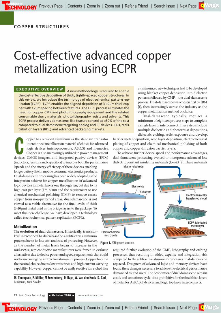
called electrochemical pattern replication (ECPR).
Metallization
Th e evolution of dual-damascene. Historically, transistor-
level interconnect has been based on a subtractive aluminum
process due to its low cost and ease of processing. However,
as the number of metal levels began to increase in the
mid-1990s, semiconductor manufacturers were forced to evaluate
alternatives due to device power and speed requirements that could
not be met using the subtractive aluminum process. Copper became
the natural choice due its low resistance and high current carrying
capability. However, copper cannot be easily reactive ion etched like
aluminum, so new techniques had to be developed
using blanket copper deposition into dielectric
patterns followed by CMP – the dual-damascene
process. Dual-damascene was chosen fi rst by IBM
[1], then increasingly across the industry as the
copper metallization method of choice.
Dual-damascene typically requires a
minimum of eighteen process steps to complete
a single layer of interconnect. Th ese steps include
multiple dielectric and photoresist depositions,
dielectric etching, resist exposure and develop,
barrier metal deposition, seed layer deposition, electrochemical
plating of copper and chemical mechanical polishing of both
copper and copper diff usion barrier layers.
To achieve further device speed and performance advantages,
dual damascene processing evolved to incorporate advanced low
dielectric constant insulating materials (low-k) [2]. Th ese materials
required further evolution of the CMP, lithography and etching
processes, thus resulting in added expense and integration risk
compared to the subtractive aluminum processes dual-damascene
replaced. Designers of advanced logic and memory devices have
found these changes necessary to achieve the electrical performance
demanded by end users. Th e economics of dual damascene remain
costly and sometimes cycle-time prohibitive for the fi nal thick layers
of metal for ASIC, RF devices and logic top layer interconnects.M. Thompson, P. Möller, M Fredenberg, D. Hays, W. Van den Hoek, D. Carl,Replisaurus, Kista, Sweden
Figure 1. ECPR process sequence.
Previous Page | Contents | Zoom in | Zoom out | Refer a Friend | Search Issue | Next PageDC B
A
M SaGEF
Previous Page | Contents | Zoom in | Zoom out | Refer a Friend | Search Issue | Next PageDC B
A
M SaGEF
6
0 20 40 60 80 100 120 0 20 40 60 80 100 120
5
4
3
2
1
0
6
5
4
3
2
1
0
Thickness
(μm)
a) b)
Thickness
(μm)
Thickness half range: +/-42%Thickness half range: +/-7%
Through-mask platingECPR printing
Linewidth (μm) Linewidth (μm)
www.solid-state.com ■ October 2010 ■ Solid State Technology 13
Th rough-mask plating. Th rough-mask
plating is another production approach to
producing copper patterns without requiring a
copper pattern-etch process. Th is method has
been widely utilized in the advanced semicon-
ductor packaging arena for the redistribution
layer (RDL) process.
Th rough-mask plating typically requires
twelve steps. Th e fi rst four steps are spin-on of
a photo sensitive dielectric layer, exposure and
develop of this layer, followed by a descum process. Th e remaining eight
steps of the through-mask plating process sequence consist of seed
deposition, the spin-on, exposure, develop of the photoresist, descum,
plating, resist strip, and fi nally, seed etch.
Th rough-mask plating, while signifi cantly lower in cost than dual-
damascene, is limited in its ability to produce thick, closely-spaced
features without re-entrant metal sidewalls. In addition, the minimum
resolvable space achieved with this technology for thick (>5μm) lines
is on the order of 10μm, thus limiting
the number of interconnects that can be
routed between the pads in an RDL layer.
Th ese limitations, which are beginning
to impact advanced logic packaging,
have created a market need for a new
methodology that will provide simple,
cost-eff ective processing for thick, fi nely-
spaced copper metal features.
Th e future: ECPR. ECPR combines
the precision and resolution of advanced
lithography with the efficiency of
electrochemical deposition into a single
electrochemical metal printing step
[3,4]. ECPR uniquely combines high
resolution, dimensional accuracy, high metal deposition rates and
low cost per layer, thereby bridging the gap between front-end of line
and back-end of line metallization methodologies.
ECPR process fl ow
Compared to the eighteen process sequences for dual damascene and
the twelve for through-plating, ECPR requires only seven steps. Th e
fi rst four, spin-on of a photo sensitive dielectric layer, exposure and
develop of this layer, followed by a descum process, are identical to
the through-mask plating sequence. Th e deposition of a barrier / seed
layer on top of a patterned photoactive dielectric, the printing of the
metal layer as the pattern is defi ned by the electrode (from this point
forward to be known as the master) utilized during the printing of
the metal and the fi nal seed etch step. Note that the latter two are
performed in the Integrated ECPR tool. Th e physics and electro-
chemistry of the ECPR plating process provides market-leading metal
thickness uniformity within die and across the wafer by design, thus
eliminating the need for post-metal deposition CMP.
ECPR’s simplicity lies in the use of a patterned electrode (the
master as defi ned above) which is pre-fi lled with copper. Th e pre-fi ll
is performed using conventional electroplating. Th e copper that is
pre-fi lled into the master is then partially trans-
ferred (printed) onto the target wafer during the
ECPR process (Fig. 1). Th is pre-fi ll is done in
parallel with other wafer processing activities
in an integrated ECPR production tool. Th e
master is reusable unlike the temporary photo-
resist template or mandrel utilized in through-
mask plating.
As no lithography is required for the metal
defi nition portion of the ECPR process, the
investment in spin coaters, exposure and develop tools and resist
materials (including solvents typically used to process the resist)
is eliminated, further reducing operational costs and total capital
investment. Typically, eight diff erent tools are required in through-
mask plating: a seed PVD tool, a resist coater, an exposure tool, a resist
developer track, a descum tool, an electroplating tool, a resist strip tool
and a seed etch tool. A single ECPR tool can replace seven of these
eight tools. A PVD seed tool and an ECPR tool combined deliver an
entire metallization line used to create one layer of patterned copper
on the wafer. Integration of the pre-fi ll, master cleaning, and seed
layer etch into a single ECPR tool also eliminates additional wafer
handling and queuing between individual tools, thereby reducing
both fab cycle time and cost.
ECPR master: a unique pattern transfer element
Th e master is patterned using advanced lithography tools and micro-
electrical-mechanical systems (MEMS)-like etching processes
found in standard CMOS fabs. Th e base material for a master is
silicon substrate sized for the dimension of the target product wafer.
Advanced lithography techniques are used to defi ne the features on
the master. Th ese sub-micron resolution features are then repeatedly
transferred to high resolution printed copper patterns without the
need for subsequent lithography.
During the ECPR process, the master is brought into contact with the
target wafer creating micro plating-cells across the target wafer surface.
Th ese micro cells, between the electrode embedded in the master and
the target wafer, signifi cantly reduce the volume of electrolytic solution
required to transfer (“plate”) the copper features from the master to the
target wafer compared to traditional through-mask plating.
Figure 2. Copper coil structure: 10μm-thick, 5μm spac-
ing, 20μm-wide.
Figure 3. As-plated copper thickness uniformity for ECPR and through-mask plating using the same mask pattern.
Previous Page | Contents | Zoom in | Zoom out | Refer a Friend | Search Issue | Next PageDC B
A
M SaGEF
Previous Page | Contents | Zoom in | Zoom out | Refer a Friend | Search Issue | Next PageDC B
A
M SaGEF
Bottom master
alignment mark
Top wafer
alignment
mark
2.3
2
2.3
2
XY Theta adjustment
0.2
0.15
0.1
0.05
0
-0.05
-0.1
-0.150 5 10 15 20 25 30 35
μm
Align error YL
Align error XR
Align error YR
14 Solid State Technology ■ October 2010 ■ www.solid-state.com
Copper structures continued from page 13
Sidewall performance
Advanced MEMS and CMOS process technology yields near-vertical
sidewalls of the features in the master, which translate into near-
vertical sidewalls of the copper patterns on the target wafer. Th is
eliminates one of the problems commonly found with through-
mask plating, i.e. the tendency for the exposed and developed resist
patterns to display curved sidewalls as the thickness increases with
decreasing line spacing. ECPR can produce features with aspect ratios
of 2:1 or greater where line spacing is ≥3μm, and line thickness is
≥5μm. Th ese results have proven to be very diffi cult to achieve with
through-mask plating. Figure 2 illustrates the capabilities of ECPR
to produce these thick, fi ne-pitch metal structures. Th ese types
of structures are increasingly important to the implementation of
integrated passives on advanced RF devices for mobile electronics
such as those which integrate WLAN, Bluetooth and GPS function-
ality into a single die.
Printed copper within die uniformity by design
The variability of line width and spacing causes thickness
non-uniformity problems for through-mask plating
due to the diff erence in localized electrical fi eld
densities caused by the diff erent opening sizes in
the plating template. Areas with low pattern density
experience higher current density, resulting in accel-
erated localized plating rates and therefore thicker
deposits. Areas with high pattern density experience
lower plating rates (due to much lower current
densities), and therefore produce slower plating rates
and proportionally thinner deposits. Th e combi-
nation of the two creates non-uniformities in the
resulting copper thickness, which is problematic for
IPDs as well as for power devices that are designed to maximize the
thickness of the copper deposited in order to reduce series resistance.
Micro cells are, by design, pattern insensitive as they isolate each and
every feature to be printed into a unique small plating cell. Th e micro
cell for one line, for example, is electrochemically isolated from the
next large pad or other feature – thus eliminating any transport eff ects
or current crowding that would lead to copper thickness variation as
a function of feature size. Th is leads to a fundamental improvement
in as-plated copper thickness uniformity. Figure
3 shows a side-by-side comparison on the same
single level copper metal process monitor electric
test structure with a wide range of line widths, line
spacing and pattern density. ECPR plated copper
thickness uniformity half-range for this vehicle
was 7% within a die; through-mask plating yielded
a thickness uniformity half-range of 42%.
Th is improved uniformity, together with the
vertical sidewalls of printed metal patterns, help to
reduce the (design – produce – measure – redesign)
cycle times required today for sophisticated RF
devices. ECPR’s highly predictable process off ers
“What you draw in CAD is what you get on your
wafer,” and will require fewer simulations and/or
evaluation cycles during pre-production verifi cation. In addition,
a higher percentage of top-performing die should be realized from
each wafer, reducing the distribution being realized at wafer-probe
during the binning process.
Th is “by design” process result for ECPR is in contrast to both
dual-damascene and through-mask plating both of which have
signifi cant challenges dealing with a wide variety of line widths
and line spaces on the same chip. In the case of dual-damascene,
the polishing rate is faster where there are dense narrow metal
features and slower where there are isolated narrow metal features,
so dishing and/or cupping of the polished surface can occur. Th e
ECPR process eliminates the considerable cost and time required
to integrate additional dummy (also known as “slotting”) features
into the layout of the dual-damascene structures that older processes
required to minimize the CMP dishing eff ects.
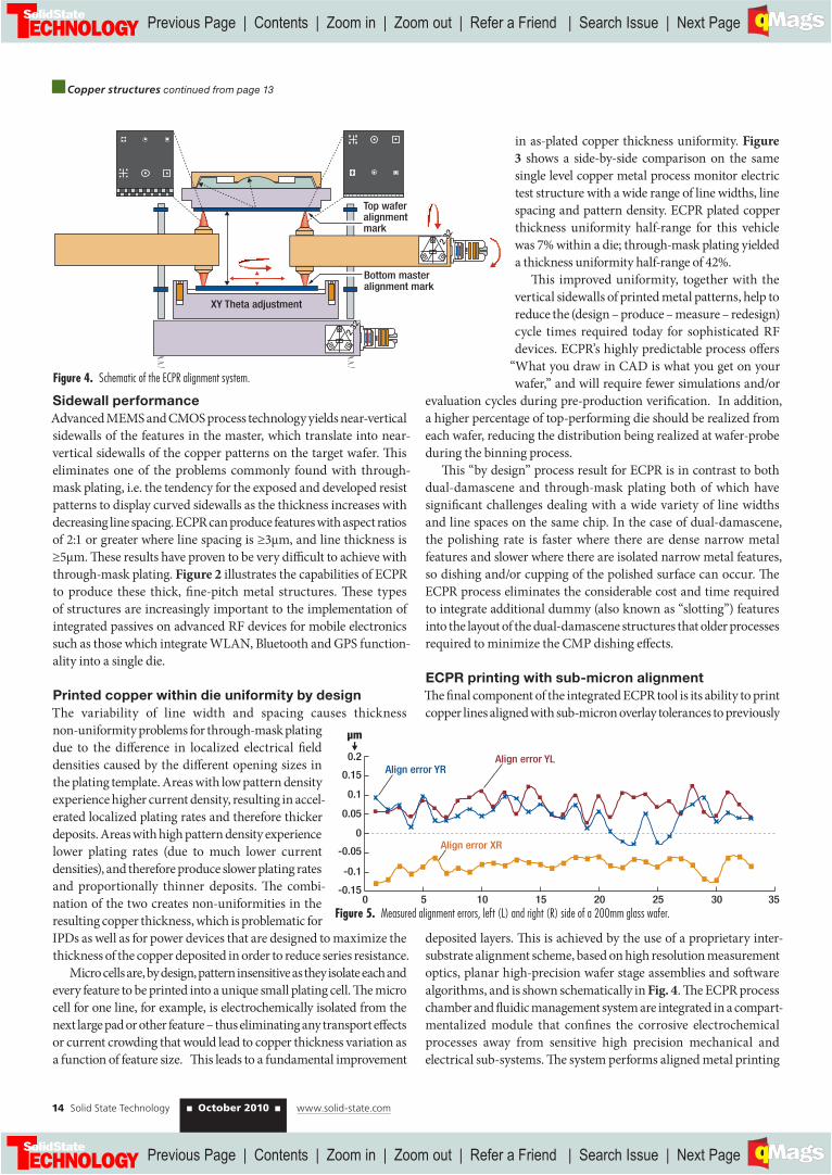
ECPR printing with sub-micron alignment
Th e fi nal component of the integrated ECPR tool is its ability to print
copper lines aligned with sub-micron overlay tolerances to previously
deposited layers. Th is is achieved by the use of a proprietary inter-
substrate alignment scheme, based on high resolution measurement
optics, planar high-precision wafer stage assemblies and soft ware
algorithms, and is shown schematically in Fig. 4. Th e ECPR process
chamber and fl uidic management system are integrated in a compart-
mentalized module that confi nes the corrosive electrochemical
processes away from sensitive high precision mechanical and
electrical sub-systems. Th e system performs aligned metal printing
Figure 4. Schematic of the ECPR alignment system.
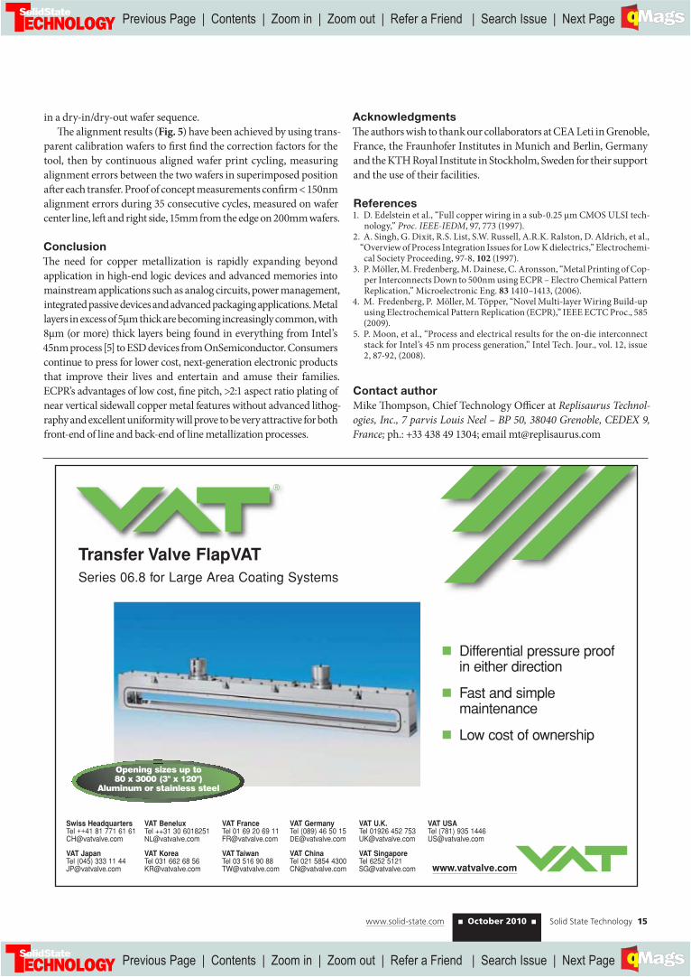
Figure 5. Measured alignment errors, left (L) and right (R) side of a 200mm glass wafer.
Previous Page | Contents | Zoom in | Zoom out | Refer a Friend | Search Issue | Next PageDC B
A
M SaGEF
Previous Page | Contents | Zoom in | Zoom out | Refer a Friend | Search Issue | Next PageDC B
A
M SaGEF
Swiss HeadquartersTel ++41 81 771 61 [email protected]
VAT GermanyTel (089) 46 50 [email protected]
VAT JapanTel (045) 333 11 [email protected]
VAT USATel (781) 935 [email protected]
VAT U.K.Tel 01926 452 [email protected]
VAT BeneluxTel ++31 30 [email protected]
VAT KoreaTel 031 662 68 [email protected]
VAT FranceTel 01 69 20 69 [email protected]
VAT TaiwanTel 03 516 90 [email protected]
VAT ChinaTel 021 5854 [email protected]
VAT SingaporeTel 6252 [email protected] www.vatvalve.com
Transfer Valve FlapVATSeries 06.8 for Large Area Coating Systems
Opening sizes up to80 x 3000 (3" x 120")
Aluminum or stainless steel
� Differential pressure proof in either direction
� Fast and simplemaintenance
� Low cost of ownership
www.solid-state.com ■ October 2010 ■ Solid State Technology 15
in a dry-in/dry-out wafer sequence.
Th e alignment results (Fig. 5) have been achieved by using trans-
parent calibration wafers to fi rst fi nd the correction factors for the
tool, then by continuous aligned wafer print cycling, measuring
alignment errors between the two wafers in superimposed position
aft er each transfer. Proof of concept measurements confi rm < 150nm
alignment errors during 35 consecutive cycles, measured on wafer
center line, left and right side, 15mm from the edge on 200mm wafers.
Conclusion
Th e need for copper metallization is rapidly expanding beyond
application in high-end logic devices and advanced memories into
mainstream applications such as analog circuits, power management,
integrated passive devices and advanced packaging applications. Metal
layers in excess of 5μm thick are becoming increasingly common, with
8μm (or more) thick layers being found in everything from Intel’s
45nm process [5] to ESD devices from OnSemiconductor. Consumers
continue to press for lower cost, next-generation electronic products
that improve their lives and entertain and amuse their families.
ECPR’s advantages of low cost, fi ne pitch, >2:1 aspect ratio plating of
near vertical sidewall copper metal features without advanced lithog-
raphy and excellent uniformity will prove to be very attractive for both
front-end of line and back-end of line metallization processes.
Acknowledgments
Th e authors wish to thank our collaborators at CEA Leti in Grenoble,
France, the Fraunhofer Institutes in Munich and Berlin, Germany
and the KTH Royal Institute in Stockholm, Sweden for their support
and the use of their facilities.
References
1. D. Edelstein et al., “Full copper wiring in a sub-0.25 μm CMOS ULSI tech-nology,” Proc. IEEE-IEDM, 97, 773 (1997).
2. A. Singh, G. Dixit, R.S. List, S.W. Russell, A.R.K. Ralston, D. Aldrich, et al., “Overview of Process Integration Issues for Low K dielectrics,” Electrochemi-cal Society Proceeding, 97-8, 102 (1997).
3. P. Möller, M. Fredenberg, M. Dainese, C. Aronsson, “Metal Printing of Cop-per Interconnects Down to 500nm using ECPR – Electro Chemical Pattern Replication,” Microelectronic Eng. 83 1410–1413, (2006).
4. M. Fredenberg, P. Möller, M. Töpper, “Novel Multi-layer Wiring Build-up using Electrochemical Pattern Replication (ECPR),” IEEE ECTC Proc., 585 (2009).
5. P. Moon, et al., “Process and electrical results for the on-die interconnect stack for Intel’s 45 nm process generation,” Intel Tech. Jour., vol. 12, issue 2, 87-92, (2008).
Contact author
Mike Th ompson, Chief Technology Offi cer at Replisaurus Technol-
ogies, Inc., 7 parvis Louis Neel – BP 50, 38040 Grenoble, CEDEX 9,
France; ph.: +33 438 49 1304; email [email protected]
Previous Page | Contents | Zoom in | Zoom out | Refer a Friend | Search Issue | Next PageDC B
A
M SaGEF
Previous Page | Contents | Zoom in | Zoom out | Refer a Friend | Search Issue | Next PageDC B
A
M SaGEF
a)
b)
Source/optics
moduleLinear (1D)
detector
Area (2D)
detectorSource/optics
module
Knife
Shaper
Thin-film (polycrystalline)/substrate
16 Solid State Technology ■ October 2010 ■ www.solid-state.com
Production metrology of advanced metallization structures using XRR and WA-XRD
INTERCONNEC T METROLOGY
The technology nodes of 45nm and
beyond pose aggressive requirements on copper metallization processes.
Barrier and seed layers become thinner; aspect ratios become higher.
Barrier and Cu seed fi lms must offer electrical continuity for the electro-
plating process and provide optimal Cu orientation for minimum resis-
tance, while maintaining conformality with smooth morphology and no
overhang [1]. These demands facilitate need for the thickness and struc-
tural characterization after seed/barrier manufacturing step. A solution
is developed based on combination of x-ray refl ectometry (XRR) and 2D
wide angle x-ray diffraction (WA-XRD) techniques.
E XECUTIVE OVE RVIE W
As the semiconductor industry continues to evolve, much
smaller and higher aspect ratio features are required for high
performance or low power devices. For such devices,
copper has replaced aluminum as the main element
used in interconnects from the fi rst to the last metal layer. Th e
advantage of copper is that it has the second highest electrical
conductivity of any element, just aft er silver, but is much more
common and hence less expensive. However, copper is very
mobile in silicon and it readily diff uses into other layers and
contaminates them. Th e solution for this problem is to deposit
a barrier layer such as tantalum, yet again, however, there are
issues in that tantalum can be deposited in more than one
crystallographic phase, each with very diff erent electrical resis-
tivities. Th e α-Ta phase has a much lower resistivity compared
to the β-phase and is therefore desirable.
Not only is the phase of the barrier important but so too is
the orientation distribution of its grains, i.e., crystallographic
texture. Th e tantalum layer is deposited in a (111) orientation
and therefore exhibits low compressive stress and facilitates a
strong preferred (111) texture in the subsequently deposited Cu
seed layer, which is desirable since such a texture has been shown
to have much better electromigration performance and hence
lifetime. Since microstructure has such a profound infl uence
on the performance and lifetime of Cu interconnects, it should be
evident that there is great benefi t in the metrology of microstruc-
tural parameters.
To be able to cope with all the challenges,
one has to carefully monitor Cu metallization
processes. We have combined two X-ray based
techniques on a single fab-proven platform: one
is X-ray refl ectivity (XRR) and the other is wide-
angle X-ray diff raction (WA-XRD).
X-ray reflectometry (XRR) is a new, but
nonetheless fi rmly established technique [2,3].
XRR is one of the most accurate thin-fi lm charac-
terization methods available as it does not make
use of material parameters that are not precisely known. Until
recently, the XRR method had suff ered from some limitations such as,
long data collection times (typically tens of minutes), large spot size,
and complex mechanics (moving sample and detectors) that resulted
in low performance and high maintenance. Th e “fast XRR method”
was specifi cally developed to overcome these issues to provide fast,
reliable XRR measurements for high-volume production.
Wide-angle X-ray diff raction (WA-XRD) has been used for the
Asaf Kay, Alex Tokar, Jordan Valley Semiconductors, Ltd., Migdal
Ha’Emek, Israel; Matthew Wormington, Jordan Valley Semiconductors, Ltd., Austin, TX USA
Figure 1. Schematic diagrams of the Jordan Valley a) XRR and b) WA-XRD channels.
Previous Page | Contents | Zoom in | Zoom out | Refer a Friend | Search Issue | Next PageDC B
A
M SaGEF
Previous Page | Contents | Zoom in | Zoom out | Refer a Friend | Search Issue | Next PageDC B
A
M SaGEF
5
4
3
2
1
0 0.4 0.8 1.2 1.6 2.0 2.4 2.8 3.2 3.6
Reflectivity
Theta, deg.
Layer
CuO
Cu
Ta
TaSi2
Si
T(A)
64.97
672.29
139.43
40.00
Sub.
D(g/cc)
1.507
8.832
15.923
14.002
2.300
R(A)
7.5
24.2
6.6
13.8
2.1
40
30
20
0 0 10 20 30 40
2θ2θ
φ
10 20 30 40
10
0
mm mm
mm
40
30
20
10
0
mm
Cu 111Cu 111
Cu 200Cu 200
Cu 111Cu 111
TaTa
Acquisition time: 100sAcquisition time: 100s
φ
www.solid-state.com ■ October 2010 ■ Solid State Technology 17
lab-based characterization of thin, polycrystalline fi lms for many
years [4]. However, the spot-size of the X-ray beam was oft en large and
the measurement speed is slow, since scanning a point (0D) detector
was commonly used. Th is has limited the use of the technique for
in-line or patterned wafer metrology. To address these issues, we
developed a WA-XRD measurement channel optimized for copper
structure metallization processes.
XRR channel
X-ray refl ectivity (XRR) is a non-destructive, standard-less technique
for the measurement of multilayer properties such as thickness,
density, and roughness. XRR measurements are highly sensitive to
the electron density of sub-micron structures irrespective of their
crystalline nature.
Consider an X-ray beam illumi-
nating the surface of a sample at
low (1-2°) incidence angle as shown
in Fig. 1a. Th e index of refraction
for all materials in the hard X-ray
wavelength region is slightly less
than one, consequently, the X-ray
beam is totally reflected if the
incidence angle is a smaller than a
certain critical angle. In this region,
the penetration depth is only a
few nanometers. At slightly higher
angles, the X-rays start to penetrate
and are refl ected from the interfaces
of thin-fi lms resulting is a series of
interference fringes.
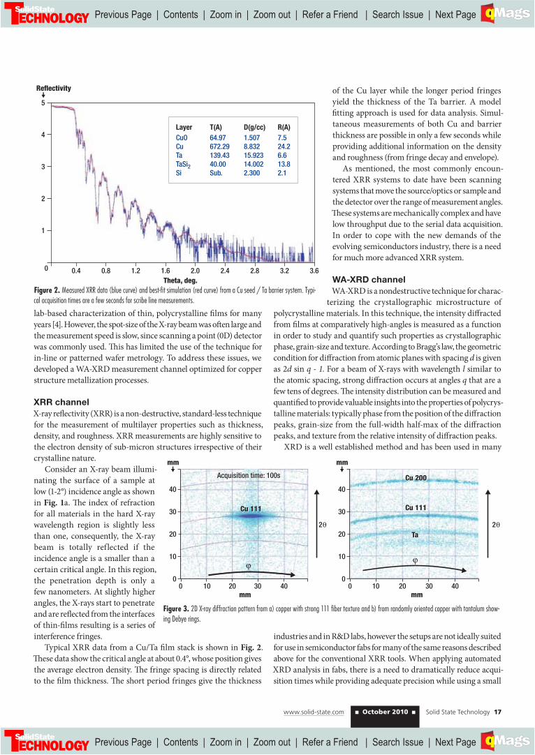
Typical XRR data from a Cu/Ta fi lm stack is shown in Fig. 2.
Th ese data show the critical angle at about 0.4°, whose position gives
the average electron density. Th e fringe spacing is directly related
to the fi lm thickness. Th e short period fringes give the thickness
of the Cu layer while the longer period fringes
yield the thickness of the Ta barrier. A model
fi tting approach is used for data analysis. Simul-
taneous measurements of both Cu and barrier
thickness are possible in only a few seconds while
providing additional information on the density
and roughness (from fringe decay and envelope).
As mentioned, the most commonly encoun-
tered XRR systems to date have been scanning
systems that move the source/optics or sample and
the detector over the range of measurement angles.
Th ese systems are mechanically complex and have
low throughput due to the serial data acquisition.
In order to cope with the new demands of the
evolving semiconductors industry, there is a need
for much more advanced XRR system.
WA-XRD channel
WA-XRD is a nondestructive technique for charac-
terizing the crystallographic microstructure of
polycrystalline materials. In this technique, the intensity diff racted
from fi lms at comparatively high-angles is measured as a function
in order to study and quantify such properties as crystallographic
phase, grain-size and texture. According to Bragg’s law, the geometric
condition for diff raction from atomic planes with spacing d is given
as 2d sin q - 1. For a beam of X-rays with wavelength l similar to
the atomic spacing, strong diff raction occurs at angles q that are a
few tens of degrees. Th e intensity distribution can be measured and
quantifi ed to provide valuable insights into the properties of polycrys-
talline materials: typically phase from the position of the diff raction
peaks, grain-size from the full-width half-max of the diff raction
peaks, and texture from the relative intensity of diff raction peaks.
XRD is a well established method and has been used in many
industries and in R&D labs, however the setups are not ideally suited
for use in semiconductor fabs for many of the same reasons described
above for the conventional XRR tools. When applying automated
XRD analysis in fabs, there is a need to dramatically reduce acqui-
sition times while providing adequate precision while using a small
Figure 2. Measured XRR data (blue curve) and best-fi t simulation (red curve) from a Cu seed / Ta barrier system. Typi-
cal acquisition times are a few seconds for scribe line measurements.
Figure 3. 2D X-ray diffraction pattern from a) copper with strong 111 fi ber texture and b) from randomly oriented copper with tantalum show-
ing Debye rings.
Previous Page | Contents | Zoom in | Zoom out | Refer a Friend | Search Issue | Next PageDC B
A
M SaGEF
Previous Page | Contents | Zoom in | Zoom out | Refer a Friend | Search Issue | Next PageDC B
A
M SaGEF
Intensity a) b)Intensity
4000
2000
200
400
600
33 36 39 42
111
45 48 51 33 36 39
Ta
Cu 200
Cu 111
42 45 48 51
2*Theta, deg 2*Theta, deg
18 Solid State Technology ■ October 2010 ■ www.solid-state.com
Interconnect metrology continued from page 17
spot so as to allow measurements on patterned wafers. We have
developed a WA-XRD channel that can be applied in fabs; it has a very
short acquisition times (from a few seconds to a few tens of seconds)
and is designed for high-volume production use. Both the hardware
and soft ware have been optimized for fab-based measurements.
Th e classic X-ray diff ractometer again works by scanning of the
sample and/or detector over very wide angular ranges. Th is leads to
signifi cant mechanical complexity due to the stability that is required
for accurate and precision positioning of a small X-ray beam over a
large wafer area. While such measurements are certainly possible,
they can be very time consuming taking many minutes and, for
some measurements, several hours. Th e JVX WA-XRD channel has
no moving source/detector and acquires data over a wide range of
diff raction angles with single-shot acquisitions (Fig. 1b). Th e channel
was developed in such a way so as to be able to handle a number of
applications.
Th e channel has a small, high intensity X-ray spot that allows
patterned wafer measurements. A custom-designed area detector
is used to provide parallel acquisition of the 2D diff raction pattern,
which provides information about both the lattice spacings and
orientations of the polycrystalline grains. Th e phase, texture and
grain size of polycrystalline thin-fi lms can be measured and mapped
over an entire 300mm wafer (Fig. 3).
Using the 2D diff raction pattern one can extract quantitative
parameters by integrating the data to produce 1D intensity distribu-
tions that can be fi tted to analytical peak functions. If the diff racted
intensity is integrated around the direction of the Debye rings (f
direction) then one can get the familiar X-ray diff raction pattern –
intensity as a function of 2q– from which phase and grain-size infor-
mation can be extracted. Th e phase of the Ta(N) barrier is important
since it infl uences the material’s resistivity and likewise for texture
and grain-size in the overlying copper (Fig. 4).
If, however, one integrates the intensity of the diff raction over the
2q direction, then one will get intensity as a function of f. Analysis
of such data provides a quantitative estimation about texture, which
has been shown to infl uence CMP erosion rates and electromigration
performance in copper interconnects.
Conclusion
Th e XRR and WA-XRD
techniques and their appli-
cation to advanced Cu
metallization are briefl y
described in this article.
Both are well established
techniques for measuring
thickness, density and
roughness (through XRR)
and grain size, texture and
crystallographic phase
(through WA-XRD). Th e
difficulties associated
with traditional X-ray
systems in the context of
automated, high-volume
manufacturing were highlighted.
Th e 6200iRD tool combines two measurement channels: XRR
and WA-XRD. Both channels are optimized for high-volume
silicon manufacturing because of very low measurement times
(a few seconds), small spot-size, and mechanical precision and
stability. Th e combination of these two channels provides compre-
hensive metrology to the metallization processes: one can monitor
the thickness and the density of the copper and barrier layers while
also obtaining valuable microstructure information in terms of phase,
grain-size, and texture. ■
References
1. P. H. Haumesser, et al., “Copper Deposition: Challenges at 32nm,” Semicon-ductor Fabtech 29, (2006), 108-114.
2 . C. Wyon, “X-ray Metrology for Advanced Microelectronics,” Eur. Phys. J. Appl. Phys. 49, (2010) 20101.
3. D. K. Bowen, B.K. Tanner, X-ray Metrology in Semiconductor Manufactur-ing, Taylor & Francis (2006).
4. M. Birkholz, Th in Film Analysis by X-Ray Scattering, Wiley-VCH (2006).
Biographies
Asaf Kay received BSc degrees in physics and materials science and
engineering from the Technion (IIT) – Israeli Institute of Technology.
He is an application engineer at Jordan Valley Semiconductors IL Ltd,
Migdal Ha’emek 23100, Israel; ph.: 972-4-6543666, ext. 250, email
Matthew Wormington graduated with a BSc(Hons.) in physics
from the U. of Birmingham, UK. He did graduate work at the U. of
Warwick, UK and is a senior technologist for Jordan Valley Semicon-
ductors Inc.
Alexander Tokar received an engineering degree from Steel and
Alloys Institute, Moscow, majoring in X-ray diff raction, and received
his PhD from the Israel Institute of Technology (IIT) in materials
science. He is a manager, worldwide application support at Jordan
Valley Semiconductors.
Figure 4. 1D integrated diffraction pattern from a) copper with strong 111 fi ber texture and b) from randomly oriented copper with tantalum.
Previous Page | Contents | Zoom in | Zoom out | Refer a Friend | Search Issue | Next PageDC B
A
M SaGEF
Previous Page | Contents | Zoom in | Zoom out | Refer a Friend | Search Issue | Next PageDC B
A
M SaGEF

The Largest and Fastest-
Growing HB LED and
Lighting Events WorldwideMeet face-to-face with thousands of the world’s most infl uential and
motivated manufacturers, equipment suppliers, and end-users who
come to evaluate products and services and get the information they
need to conduct business within the global LED and lighting industry.
United States (West Coast)
Tim Carli, Sales
+1 650 941 3438, x23
United States (East Coast)
Mary Donnelly, Sales
+1 603 891 9398
Sept. 29 – Oct. 1, 2010
Pacifi co Yokohama
Yokohama, Japan
www.sil-ledjapan.com
February 23 – 25, 2011
Santa Clara Convention Center
Santa Clara, CA USA
www.strategiesinlight.com
Hong Kong/Asia
Mark Mak, Sales
+852 2838 6298
Mainland China
Michael Tsui, Sales
+86 755 259 88571 x1009
Singapore/Taiwan
Michael Yee, Sales
+65 9616 8080
Europe
Virginia Willis, Sales
+44 0 1992 656 663
Germany/Austria
Holger Gerisch, Sales
+49 8801 302430
Japan
Manami Konishi, Sales
+81 3321 93 641
Record-breaking attendance 4 years
running– 2010 the largest in its
11-year history!!
Exhibit fl oor sold out in 2010
Sept. 27 – 29, 2010
Sheraton Frankfurt Hotel & Towers
Frankfurt, Germany
www.sileurope.com
May 10 – 12, 2011
Kowloon Shangri-La Hotel
Kowloon, Hong Kong
www.strategiesinlight.com
Follow the Light to Europe’s
brightest new LED & Lighting
Conference and Exhibition
Announcing!
Nearly doubled attendance set in
previous inaugural year 2008 –
5,300 total attendees in 2009!
Attendee Profi le
• LED & lighting specialists
working with:
- Mobile Appliances
- Signs and Displays
- Automotive Lighting
- Signals
- Electronic Equipment
- Illumination
• LED lighting manufacturers
• LED product designers
• LED makers & distributors
• Lighting designers,
specifi ers & architects
• Energy-effi ciency
organizations
• Corporate R&D staff
• Government regulators &
policy-makers
• Financial analysts,
investment bankers, &
venture capitalists
Whether you are a supplier, an LED manufacturer trying to reach new
customers, a designer looking for new product information, or a buyer
exploring the latest technologies, Strategies in Light can help achieve
your objectives.
Applications Include:
• General lighting/
illumination
• Architectural & decorative
lighting
• Mobile devices
• Outdoor lighting
• Signs & displays
• Automotive lighting
• Signals
• Backlighting
Who Will Exhibit
• LED manufacturers
• Component distributors
• Driver & controller
manufacturers
• Test & measurement
providers
• LED lighting manufacturers
• Design software suppliers
• Equipment & materials
suppliers
• Thermal management &
optics suppliers
• Module & light-engine
vendors
Owned and Produced by: Presented by: Flagship Media Sponsors:
For more information on exhibiting or sponsoring at ANY SIL event , please contact:
Previous Page | Contents | Zoom in | Zoom out | Refer a Friend | Search Issue | Next PageDC B
A
M SaGEF
Previous Page | Contents | Zoom in | Zoom out | Refer a Friend | Search Issue | Next PageDC B
A
M SaGEF
2.0
2001 2002 2003 2004 2005 2006 2007 2008 2009
1.6
1.2
0.8
0.4
0
Energy (kWh/cm2)
KSIA energy usage (kWh/cm2)
20 Solid State Technology ■ October 2010 ■ www.solid-state.com
Vacuum/abatement technology saves the bottom line and the planet
VACUUM
Semiconductor manufacturing, like any
business, must make a profi t, but profi tability need not come at the
expense of the environment. The latest advances in the vacuum and abate-
ment technologies, used to remove and neutralize process wastes and by-
products, are allowing manufacturers to reduce operating costs, energy
consumption and carbon footprint all at the same time. In addition, inte-
gration of vacuum and abatement capabilities in optimized, process-spe-
cifi c systems is also reducing capital expenditures and installation times.
The combined effect on total cost-of-ownership allows manufacturers to
respect both the planet and the bottom line.
E XECUTIVE OVE RVIE W
The semiconductor industry is not the only industry that has
developed a highly refi ned economic model of its manufac-
turing process; other industries that share an intense focus on
profi tability include fl at panel display (FPD), light emitting
diode (LED), and photovoltaic (PV) manufacturing. Notwith-
standing the focus on profi tability, these industries have historically
also been cognizant of the potential eff ects of the manufac-
turing processes on the global environment, and been careful
to comply with relevant regulations. Energy consumption has
been part of the industry roadmap for much of the last ten
years.
Energy consumption per cm2 of silicon declined steadily
over most of the past decade, until increases in device and
process complexity, such as the introduction of high-k
metal gates, forced up the number of process steps. Energy
consumption per cm2 actually increased from 2008 to 2009
(Fig. 1). Other new processes can be expected to put additional
upward pressure on energy consumption. For example,
extreme ultraviolet (EUV) lithography will use three to fi ve
times the energy of immersion lithography.
Vacuum and abatement account for a signifi cant portion
of the power used in semiconductor manufacturing.
Vacuum pumps represent as much as 20% of total fab energy
consumption. Exhaust gas abatement systems, which use
hydrocarbon fuels or electricity to heat and oxidize process
gases, also contribute substantially to fab energy consumption.
Th e latest developments in vacuum and abatement technology
provide signifi cant reductions in energy consumption and, because
of the large contribution these processes make to the total energy
budget, will likely play an important role in manufacturers’ eff orts to
meet their environmental goals, without adversely
aff ecting productivity or profi tability.
Vacuum pumps
Vacuum pumps off er a number of opportunities
to improve energy effi ciency. Non-contact seals,
improved bearing design and lubrication (oil
fl ow, oil type, size, and preload), and better gear
design (tooth profi le and size) can all reduce
frictional losses. Port and rotor profi les and the
number of pumping stages can be optimized for
specifi c compression and pumping performance profi les. Cooling
systems can be designed for effi cient heat transfer and minimal water
consumption, while maintaining reliability with specifi c attention
to temperature sensitive components. Th e motor and inverter can
be matched to load requirements. As an example, comparing the
current generation of Edward’s harsh duty dry pumps (iXH) with
the previous generation (iH), the combination of improvements
in all of these areas has halved ultimate pressure, reduced energy
consumption by 5% to 13% (size dependant) and signifi cantly
decreased the overall size of the pump.
Mike Czerniak, Edwards, Clevedon, North Somerset, UK
Figure 1. Energy consumption (kWh/cm2) has declined steadily over the last decade. The uptick from
2008 to 2009 is attributed to increasing device and process complexity. It brings increased pressure on man-
ufacturers to restore the downward trend. (Data from Korean Semiconductor Industry Association [1]. Other
territories show similar trends)
Previous Page | Contents | Zoom in | Zoom out | Refer a Friend | Search Issue | Next PageDC B
A
M SaGEF
Previous Page | Contents | Zoom in | Zoom out | Refer a Friend | Search Issue | Next PageDC B
A
M SaGEF
100
80
60
40
20
0
Mode 3 Mode 2 Mode 1
Saving (%)
Green idle mode
WWW.LEVITRONIX.COM
LEVIFLOW byTM
The Ultra-Pure Ultrasonic Flowmeter
With The Best Price-Performance Ratio
www.solid-state.com ■ October 2010 ■ Solid State Technology 21
Exhaust gas abatement systems
Th e simplest approach to combustion is an open fl ame combustor
in which the exhaust stream is introduced into an unconfi ned
fl ame. With this approach, conditions can vary widely within the
combustion zone, generally requiring a larger combustor and higher
fuel consumption to guarantee the reduction of hazardous compo-
nents to acceptable levels. Inward fi red combustion, a
more effi cient alternative, uses a hollow cylinder of
porous ceramic material to create a closely controlled,
isothermal combustion zone. Air and fuel fl ow inward
through the ceramic where they provide fl ameless
combustion on the ceramic surface. Th e fl ow of exhaust
gas is confi ned completely within the combustion
zone. Th e ability to maintain uniform temperature
throughout the zone maximizes fuel effi ciency and
ensures complete combustion of the exhaust stream.
Careful attention to combustor design can provide
signifi cant energy savings. For instance, current gener-
ation systems can treat up to 600slm of exhaust gas,
depending on the application and model, and typically
consume half the fuel gas required by the previous
generation.
Green mode
One of the most important developments in vacuum and abatement
components has been the full implementation of “green” or idle mode
capabilities, which reduce power consumption during idle periods.
Th e capability was fi rst introduced early in the decade and it had
become standard on most semiconductor products by 2007. However,
full realization of its potential has occurred only lately as manufac-
Figure 2. Three different idle modes provide different levels of energy savings, allowing manufacturers to maximize
savings by fi ne tuning operations while preserving suffi cient response time to meet specifi c process requirements.
Previous Page | Contents | Zoom in | Zoom out | Refer a Friend | Search Issue | Next PageDC B
A
M SaGEF
Previous Page | Contents | Zoom in | Zoom out | Refer a Friend | Search Issue | Next PageDC B
A
M SaGEF
_______________________________
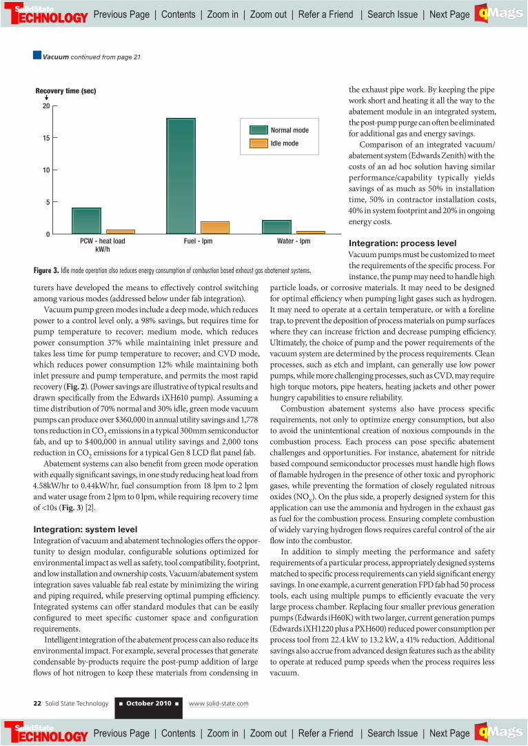
20
15
10
5
0
PCW - heat load
kW/h
Fuel - lpm Water - lpm
Normal mode
Idle mode
Recovery time (sec)
22 Solid State Technology ■ October 2010 ■ www.solid-state.com
Vacuum continued from page 21
turers have developed the means to eff ectively control switching
among various modes (addressed below under fab integration).
Vacuum pump green modes include a deep mode, which reduces
power to a control level only, a 98% savings, but requires time for
pump temperature to recover; medium mode, which reduces
power consumption 37% while maintaining inlet pressure and
takes less time for pump temperature to recover; and CVD mode,
which reduces power consumption 12% while maintaining both
inlet pressure and pump temperature, and permits the most rapid
recovery (Fig. 2). (Power savings are illustrative of typical results and
drawn specifi cally from the Edwards iXH610 pump). Assuming a
time distribution of 70% normal and 30% idle, green mode vacuum
pumps can produce over $360,000 in annual utility savings and 1,778
tons reduction in CO2 emissions in a typical 300mm semiconductor
fab, and up to $400,000 in annual utility savings and 2,000 tons
reduction in CO2 emissions for a typical Gen 8 LCD fl at panel fab.
Abatement systems can also benefi t from green mode operation
with equally signifi cant savings, in one study reducing heat load from
4.58kW/hr to 0.44kW/hr, fuel consumption from 18 lpm to 2 lpm
and water usage from 2 lpm to 0 lpm, while requiring recovery time
of <10s (Fig. 3) [2].
Integration: system level
Integration of vacuum and abatement technologies off ers the oppor-
tunity to design modular, confi gurable solutions optimized for
environmental impact as well as safety, tool compatibility, footprint,
and low installation and ownership costs. Vacuum/abatement system
integration saves valuable fab real estate by minimizing the wiring
and piping required, while preserving optimal pumping effi ciency.
Integrated systems can off er standard modules that can be easily
confi gured to meet specifi c customer space and confi guration
requirements.
Intelligent integration of the abatement process can also reduce its
environmental impact. For example, several processes that generate
condensable by-products require the post-pump addition of large
fl ows of hot nitrogen to keep these materials from condensing in
the exhaust pipe work. By keeping the pipe
work short and heating it all the way to the
abatement module in an integrated system,
the post-pump purge can oft en be eliminated
for additional gas and energy savings.
Comparison of an integrated vacuum/
abatement system (Edwards Zenith) with the
costs of an ad hoc solution having similar
performance/capability typically yields
savings of as much as 50% in installation
time, 50% in contractor installation costs,
40% in system footprint and 20% in ongoing
energy costs.
Integration: process level
Vacuum pumps must be customized to meet
the requirements of the specifi c process. For
instance, the pump may need to handle high
particle loads, or corrosive materials. It may need to be designed
for optimal effi ciency when pumping light gases such as hydrogen.
It may need to operate at a certain temperature, or with a foreline
trap, to prevent the deposition of process materials on pump surfaces
where they can increase friction and decrease pumping effi ciency.
Ultimately, the choice of pump and the power requirements of the
vacuum system are determined by the process requirements. Clean
processes, such as etch and implant, can generally use low power
pumps, while more challenging processes, such as CVD, may require
high torque motors, pipe heaters, heating jackets and other power
hungry capabilities to ensure reliability.
Combustion abatement systems also have process specifi c
requirements, not only to optimize energy consumption, but also
to avoid the unintentional creation of noxious compounds in the
combustion process. Each process can pose specifi c abatement
challenges and opportunities. For instance, abatement for nitride
based compound semiconductor processes must handle high fl ows
of fl amable hydrogen in the presence of other toxic and pyrophoric
gases, while preventing the formation of closely regulated nitrous
oxides (NOx). On the plus side, a properly designed system for this
application can use the ammonia and hydrogen in the exhaust gas
as fuel for the combustion process. Ensuring complete combustion
of widely varying hydrogen fl ows requires careful control of the air
fl ow into the combustor.
In addition to simply meeting the performance and safety
requirements of a particular process, appropriately designed systems
matched to specifi c process requirements can yield signifi cant energy
savings. In one example, a current generation FPD fab had 50 process
tools, each using multiple pumps to effi ciently evacuate the very
large process chamber. Replacing four smaller previous generation
pumps (Edwards iH60K) with two larger, current generation pumps
(Edwards iXH1220 plus a PXH600) reduced power consumption per
process tool from 22.4 kW to 13.2 kW, a 41% reduction. Additional
savings also accrue from advanced design features such as the ability
to operate at reduced pump speeds when the process requires less
vacuum.
Figure 3. Idle mode operation also reduces energy consumption of combustion based exhaust gas abatement systems.
Previous Page | Contents | Zoom in | Zoom out | Refer a Friend | Search Issue | Next PageDC B
A
M SaGEF
Previous Page | Contents | Zoom in | Zoom out | Refer a Friend | Search Issue | Next PageDC B
A
M SaGEF
www.solid-state.com ■ October 2010 ■ Solid State Technology 23
Interconnect metrology continued from page 22
EXECUTIVE OFFICES
PennWell, 98 Spit Brook Rd, Nashua, NH 03062-5737
Tel: 603/891-0123
ADVERTISING
Marcella Hanson—Ad Traffi c Manager
Rachael Caron—Marketing Communications Manager
ADVERTISING SALES OFFICES
Group PublisherDiane Lieberman, 98 Spit Brook Rd, Nashua, NH 03062-5737;
Tel: 603/891-9441; Fax: 603/891-9328;
e-mail: [email protected]
Regional Sales ManagerEast Coast US and Eastern Canada, MidwestKaren Watkins, 98 Spit Brook Rd. Nashua, NH 03062-5737
Tel: 603/891-9118; Fax: 603/891-9328;
e-mail: [email protected]
Regional Sales ManagerWest Coast US, Western CanadaLisa Zimmerer, 190 Cecil Place, Costa Mesa, CA 92627
Tel: 949/515-0552; Fax: 949/515-0553;
e-mail: [email protected]
Direct Mail DirectorBob Dromgoole, 98 Spit Brook Rd, Nashua, NH 03062-5737;
Tel: 603/891-9128; Fax: 603/891-9341;
e-mail: [email protected]
Austria, Germany, Liechtenstein, Russia, N. Switzerland, Eastern EuropeHolger Gerisch, Hauptstrasse 16,
D-82402 Seeshaupt, Germany;
Tel: 49/8801-302430; Fax: 49/8801-913220;
e-mail: [email protected]
France, Netherlands, Belgium, W. Switzerland, Spain, Greece, Portugal Luis Matutano, Adecome+, 1, rue Jean Carasso,
F-95870 Bezons, France
Tel: 33/1-30 76 55 43; Fax: 33/1-30 76 55 47;
e-mail: [email protected]
United Kingdom & Scandinavia Tony Hill, PennWell Publishing UK Ltd., Warlies Park House,
Horseshoe Hill, Hill, Upshire, Essex, U.K. EN9 3SR
Tel / Fax: 44-1442-239547
e-mail: [email protected]
IsraelDan Aronovic, Allstar Media Inc.,
3/1 Hatavas St., Kadima, 60920, Israel
Tel / Fax: 972/9-899-5813
e-mail: [email protected]
JapanManami Konishi, Masaki Mori, ICS Convention Design, Inc.,
Chiyoda Bldg., Sarugaku-cho 1-5-18,
Chiyoda-ku, Tokyo 101-8449, Japan
Tel: 3-3219-3641; Fax: 3-3219-3628;
e-mail: [email protected]
TaiwanVicky Kung, Alice Chen, Arco InfoComm, 4F-1, #5, Sec. 1,
Pa-Te Rd., Taipei, Taiwan R.O.C. 100
Tel: 886/2-2396-5128; Fax: 886/2-2395-9571;
e-mail: [email protected]
China, Hong KongAdonis Mak, ACT International, Unit B, 13/F, Por Yen Building,
478 Castle Peak Road, Cheung Sha Wan, Kowloon, Hong Kong
Tel: 852/2-838-6298; Fax: 852/2-838-2766;
e-mail: [email protected]
SingaporeAdeline Lam, Publicitas Singapore Pte Ltd.
20 Bideford Rd., #02-01, Wellington Building, Singapore 229921
Tel: 65/6836-2272; Fax: 65/6735-9653
e-mail: [email protected]
The Advertiser’s Index is published as a service. The publisher does not assume any liability for errors or omissions.
October 2010, Volume 53, Number 9 • Solid State Technology ©2010 (ISSN 0038-111X) Periodicals postage paid at Tulsa, OK 74112, & additional mailing offi ces. Member Association of Business Publishers. Published 10x per year, monthly except August and December by PennWell Corp., 1421 S. Sheridan Rd., Tulsa, OK 74112. Solid State Technology offi ces: 98 Spit Brook Rd., Nashua, NH 03062-5737, ph 603/891-0123, www.solid-state.com. Subscriptions: Domestic: one year: $258.00, two years: $413.00; one year Canada/Mexico: $360.00, two years: $573.00; one-year international airmail: $434.00, two years: $691.00; Single copy price: $15.00 in the US, and $20.00 elsewhere. Single copy rate for the special March issue that contains the Resource Guide Supplement: $139.00 in the U.S; $155.00 in Canada; $176.00 international airmail. Digital distribution: $130.00. You will continue to receive your subscription free of charge. This fee is only for air mail delivery. Address corre-spondence regarding subscriptions (including change of address) to: Solid State Technology, PO Box 3425, Northbrook, IL 60065-9595, [email protected], ph 847-559-7500 (8 am – 5 pm, CST). Include zip code and, for change of address, copy of old label. We make por-tions of our subscriber list available to carefully screened companies that offer products and services that may be important for your work. If you do not want to receive those offers and/or information, please let us know by contacting us at List Services, Solid State Technology, 98 Spit Brook Road, Nashua, NH 03062. All rights reserved. No part of this publication may be produced or transmitted in any form or by any means, electronic or mechanical, including photocopying, recording, or by any information storage retrieval sys-tem, without written permission of the copyright owner. Prices for bulk reprints of articles available on request. Solid State Technologyarticles are indexed in Engineering Information and Current Contents, and Applied Science & Technology Index and abstracted by Applied Science & Technology Abstracts.PRINTED IN THE USA. GST NO. 126813153. Publication Mail Agreement No. 40052420. POSTMASTER: Send address changes to Solid State Technology, PO Box 3425, Northbrook, IL 60065-9595. Return Undeliverable Canadian Addresses to: P.O. Box 122, Niagara Falls, ON L2E 6S4.
A D I N D E XAdvertiser Pg Advertiser Pg
CYMER ............................................................ 7
Levitronix GmbH ............................................ 21
NTK Technologies, Inc. .....................................9
NUSIL .............................................................C4
Plasmatic Systems ............................................8
REC Silicon .......................................................3
SEMI ............................................................... 11
Solid State Equipment Corporation ................C2
Strategies in Light ........................................... 19
Swagelok .........................................................5
The Confab 2011 ............................................C3
VAT INC ......................................................... 15
VITECHNOLOGY .............................................. 1
Integration: fab level
As described previously, green mode operation holds the potential for signifi cant energy
savings, contingent upon successful integration of control infrastructure in the fab.
Internal green mode switching has been standard on most semiconductor vacuum
and abatement systems since 2007. Th ese systems include a μTIM connector with pins
assigned for the switching signal. Equipment manufacturers are now beginning to
provide output signals to control the vacuum and abatement systems that support their
process tools. Th e next level of integration will be the implementation of the proposed
E30/37 standard, a much more fl exible and comprehensive communication protocol,
which will allow the manufacturing execution system (MES) to control the idle mode
status of process and ancillary equipment through active utility control (AUC). ■
References
1. Korean Semiconductor Industry Association, presented at IHTESH, HsinChu, Taiwan, June 21-23, 2010.
2. ISMI Technology Transfer Report #07124899A-ENG, 2007, available only to members of ISMI via http://ismi.sematech.org/index.htm.
Biography
Mike Czerniak received his PhD at Manchester U., and is the product marketing
manager of the Exhaust Gas Management Division of Edwards, Clevedon, North
Somerset BS21 6TH, UK; ph.: +44 (0)1275 337100; email Mike.Czerniak@edwards
vacuum.com
Previous Page | Contents | Zoom in | Zoom out | Refer a Friend | Search Issue | Next PageDC B
A
M SaGEF
Previous Page | Contents | Zoom in | Zoom out | Refer a Friend | Search Issue | Next PageDC B
A
M SaGEF
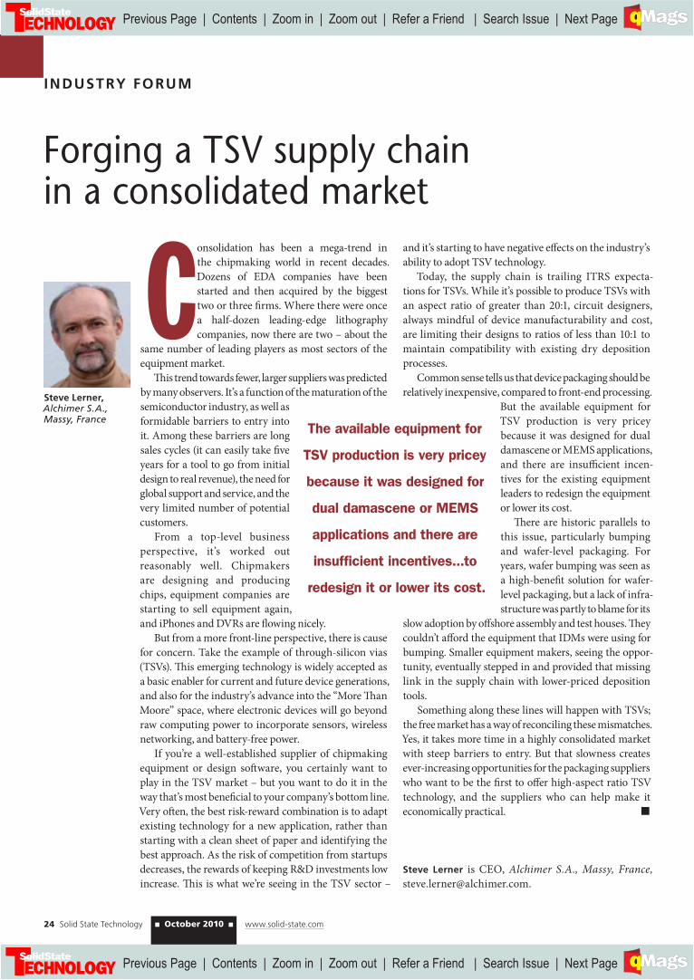
24 Solid State Technology ■ October 2010 ■ www.solid-state.com
INDUSTRY FORUM
Consolidation has been a mega-trend in
the chipmaking world in recent decades.
Dozens of EDA companies have been
started and then acquired by the biggest
two or three fi rms. Where there were once
a half-dozen leading-edge lithography
companies, now there are two – about the
same number of leading players as most sectors of the
equipment market.
Th is trend towards fewer, larger suppliers was predicted
by many observers. It’s a function of the maturation of the
semiconductor industry, as well as
formidable barriers to entry into
it. Among these barriers are long
sales cycles (it can easily take fi ve
years for a tool to go from initial
design to real revenue), the need for
global support and service, and the
very limited number of potential
customers.
From a top-level business
perspective, it’s worked out
reasonably well. Chipmakers
are designing and producing
chips, equipment companies are
starting to sell equipment again,
and iPhones and DVRs are fl owing nicely.
But from a more front-line perspective, there is cause
for concern. Take the example of through-silicon vias
(TSVs). Th is emerging technology is widely accepted as
a basic enabler for current and future device generations,
and also for the industry’s advance into the “More Th an
Moore” space, where electronic devices will go beyond
raw computing power to incorporate sensors, wireless
networking, and battery-free power.
If you’re a well-established supplier of chipmaking
equipment or design soft ware, you certainly want to
play in the TSV market – but you want to do it in the
way that’s most benefi cial to your company’s bottom line.
Very oft en, the best risk-reward combination is to adapt
existing technology for a new application, rather than
starting with a clean sheet of paper and identifying the
best approach. As the risk of competition from startups
decreases, the rewards of keeping R&D investments low
increase. Th is is what we’re seeing in the TSV sector –
and it’s starting to have negative eff ects on the industry’s
ability to adopt TSV technology.
Today, the supply chain is trailing ITRS expecta-
tions for TSVs. While it’s possible to produce TSVs with
an aspect ratio of greater than 20:1, circuit designers,
always mindful of device manufacturability and cost,
are limiting their designs to ratios of less than 10:1 to
maintain compatibility with existing dry deposition
processes.
Common sense tells us that device packaging should be
relatively inexpensive, compared to front-end processing.
But the available equipment for
TSV production is very pricey
because it was designed for dual
damascene or MEMS applications,
and there are insuffi cient incen-
tives for the existing equipment
leaders to redesign the equipment
or lower its cost.
Th ere are historic parallels to
this issue, particularly bumping
and wafer-level packaging. For
years, wafer bumping was seen as
a high-benefi t solution for wafer-
level packaging, but a lack of infra-
structure was partly to blame for its
slow adoption by off shore assembly and test houses. Th ey
couldn’t aff ord the equipment that IDMs were using for
bumping. Smaller equipment makers, seeing the oppor-
tunity, eventually stepped in and provided that missing
link in the supply chain with lower-priced deposition
tools.
Something along these lines will happen with TSVs;
the free market has a way of reconciling these mismatches.
Yes, it takes more time in a highly consolidated market
with steep barriers to entry. But that slowness creates
ever-increasing opportunities for the packaging suppliers
who want to be the fi rst to off er high-aspect ratio TSV
technology, and the suppliers who can help make it
economically practical. ■
Steve Lerner is CEO, Alchimer S.A., Massy, France,
Forging a TSV supply chain in a consolidated market
Steve Lerner,Alchimer S.A., Massy, France
The available equipment for
TSV production is very pricey
because it was designed for
dual damascene or MEMS
applications and there are
insuffi cient incentives...to
redesign it or lower its cost.
Previous Page | Contents | Zoom in | Zoom out | Refer a Friend | Search Issue | Next PageDC B
A
M SaGEF
Previous Page | Contents | Zoom in | Zoom out | Refer a Friend | Search Issue | Next PageDC B
A
M SaGEF

Meet face-to-face with senior-level executives representing the top semiconductor manufacturing companies from around the globe!
MAY 15 - 18, 2011M RESORT SPA CASINOLAS VEGAS, NEVADA
2011www.theconfab.com
Owned and Produced by: Flagship Media Sponsors:
THE POWER OF ONE EVENT
Hear a World-Class Conference Program Built for the Benefi t
of Device Manufacturers and Th eir Global Suppliers
Meet Senior-Level Executives from the Semiconductor Supplier
and Manufacturing Community
Participate in Private Face-to Face Boardroom Meetings with
Guaranteed ROI
Contact Jo-Ann Pelligrini for more
information on sponsorships and
customized programs at (650) 946.3169
or email [email protected]
Previous Page | Contents | Zoom in | Zoom out | Refer a Friend | Search Issue | Next PageDC B
A
M SaGEF
Previous Page | Contents | Zoom in | Zoom out | Refer a Friend | Search Issue | Next PageDC B
A
M SaGEF

The lifesaving microchip never failed thanks to a powerful
protective silicone coating created by NuSil.
It’s part of our extensive line of low-outgassing materials
designed and tested to perform with low contamination
in harsh environments and extreme thermal conditions.
At NuSil, our scientists are dedicated to helping innovators
innovate. Whether your needs are for large batches or
small, you can depend on the leader in silicone solutions
with nearly 30 years of electronics experience.
We want every product story to have a happy ending.
What? When? Where? If it’s NuSil, it’s no problem.
Lost puppy.
Implanted microchip.
Welcome home, Lucky.
NuSil Technology.
What’s your challenge? www.nusil.com/ap USA +1-805-684-8780Europe +33 (0) 4 92 96 93 31©2010 NuSil Technology LLC. All rights reserved. AP0410-E
Previous Page | Contents | Zoom in | Zoom out | Refer a Friend | Search Issue | Next PageDC B
A
M SaGEF
Previous Page | Contents | Zoom in | Zoom out | Refer a Friend | Search Issue | Next PageDC B
A
M SaGEF