Embed Size (px)
Citation preview
The Physics of Soft-Breakdown andits Implications for Integrated Circuits
Muhammad Ashraful Alam
in collaboration with
B. Weir, P. Silverman, and R. K. SmithAgere Systems, PA 18109
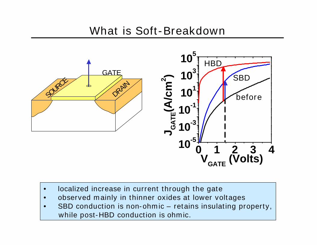
What is Soft-Breakdown
• localized increase in current through the gate• observed mainly in thinner oxides at lower voltages• SBD conduction is non-ohmic – retains insulating property,
while post-HBD conduction is ohmic.
GATE
SOURCE
DRAIN
0 1 2 3 410-5
10-3
10-1
101
103
105
J GA
TE(A
/cm
2 )VGATE (Volts)
before
SBD
HBD
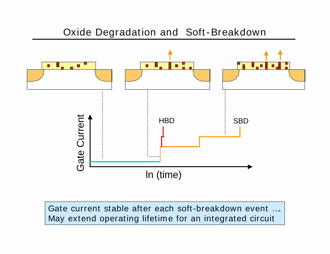
Oxide Degradation and Soft-Breakdown
ln (time)
Gat
e C
urre
nt SBDHBD
Gate current stable after each soft-breakdown event ….May extend operating lifetime for an integrated circuit
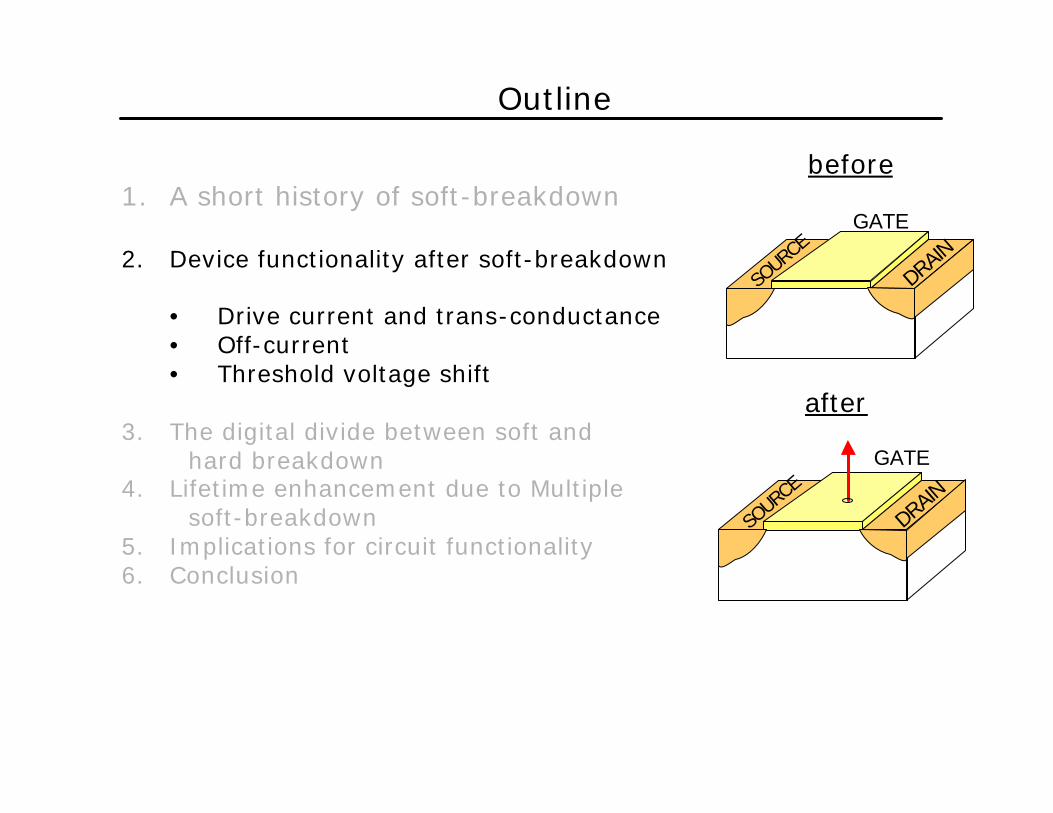
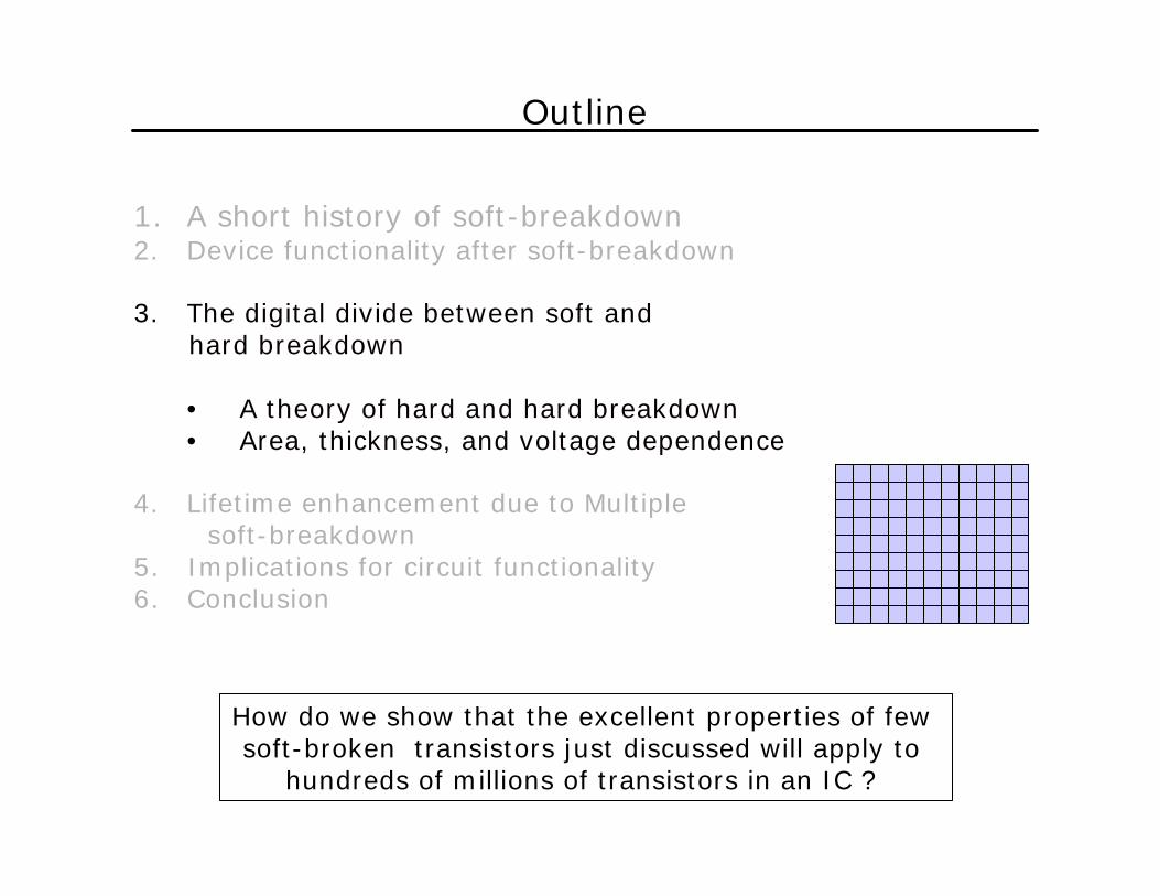
Outline
1. A short history of soft-breakdown research
2. Device functionality after soft-breakdown
3. The digital divide between soft and hard breakdown
4. Lifetime enhancement due to multiple soft-breakdown
5. Implications for circuit functionality
6. Conclusion
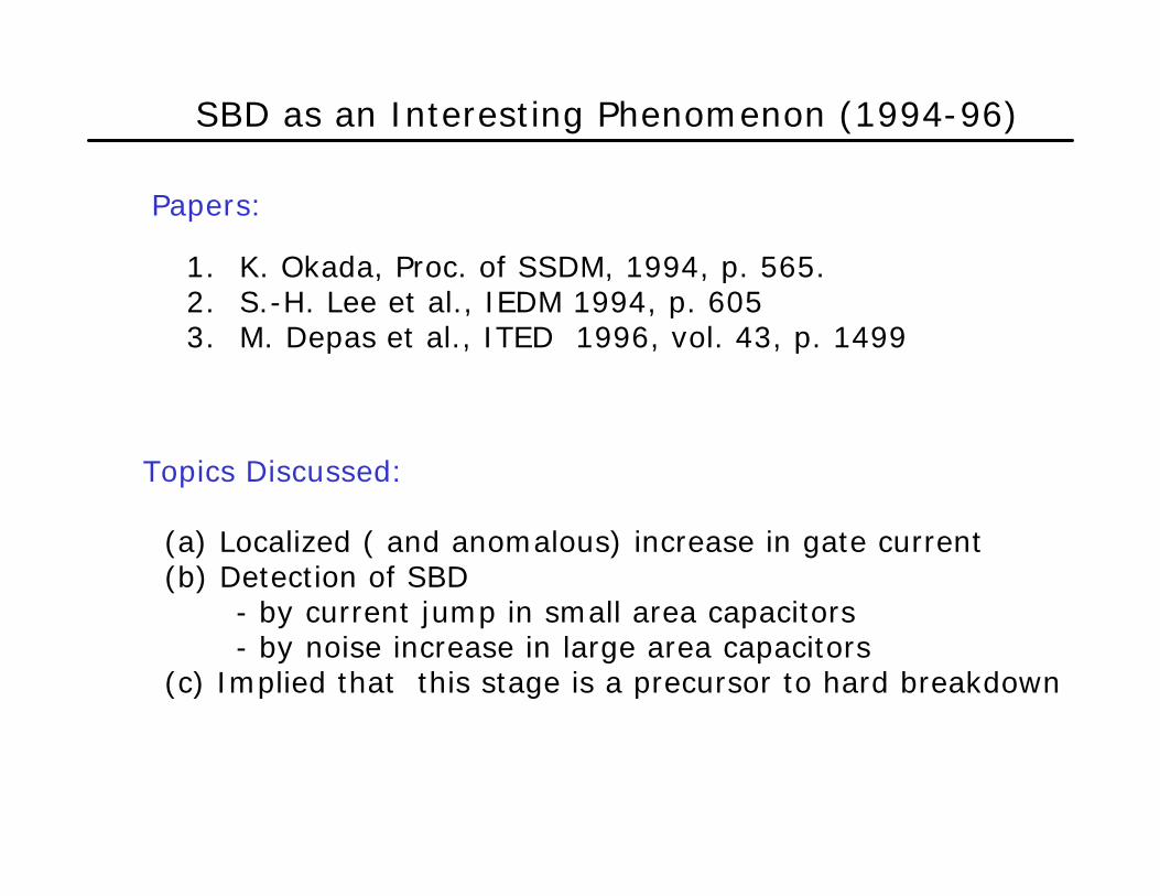
SBD as an Interesting Phenomenon (1994-96)
1. K. Okada, Proc. of SSDM, 1994, p. 565. 2. S.-H. Lee et al., IEDM 1994, p. 6053. M. Depas et al., ITED 1996, vol. 43, p. 1499
Topics Discussed:
(a) Localized ( and anomalous) increase in gate current(b) Detection of SBD
- by current jump in small area capacitors- by noise increase in large area capacitors
(c) Implied that this stage is a precursor to hard breakdown
Papers:

SBD vs. NMOS Reliability (1995-1999)
1. R. Degraeve et al., ITED 1998, p. 904 - Weibull slope decreases with oxide thickness
2. J. Stathis and D. DiMaria, IEDM 1998, p. 167- trap generation rate reduces exponentially
with voltage with a constant voltage acceleration factor
Topics Discussed:
(a) dependence of soft-breakdown on operating voltage,oxide area, and thickness.
(b) influence of soft-breakdown on transistor characteristics
Papers with NMOS TDDB Concerns:
SBD Papers:
1. B. Weir et al., IEDM 1997, p. 732. E. Wu et al., IEDM 1998, p. 187
1E-5 1E-4 1E-3 0.01 0.1 1
1
2
3
4
5
6
Pos
tbd
Vol
tage
Capacitor Area (cm2)
-4 -5 -6 -7 -8-0
-1
-2
-3
-4
-5
Stress at -1mA/cm2
3.5nm 4.0nm 5.0nm 6.5nmVpo
stbd
Vstart
-4 -5 -6 -7 -8-0
-1
-2
-3
-4
-54.0 nm oxide
-0.1mA/cm2
-1mA/cm2
-10mA/cm2
-100mA/cm2
Vpo
stbd
Vstart
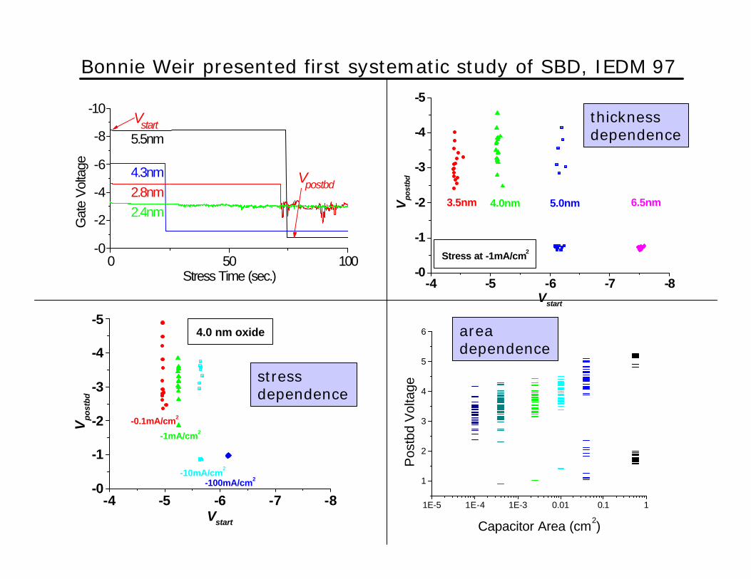
Bonnie Weir presented first systematic study of SBD, IEDM 97
0 50 100-0
-2
-4
-6
-8
-10
Vpostbd
Vstart
2.4nm
5.5nm
4.3nm2.8nm
Gat
e V
olta
ge
Stress Time (sec.)
stressdependence
areadependence
thicknessdependence
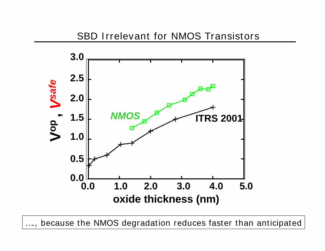
SBD Irrelevant for NMOS Transistors
3.0
2.0
1.5
1.0
0.0
0.5
2.5
0.0 1.0 2.0 3.0 4.0 5.0oxide thickness (nm)
Vop
, V
safe
NMOS ITRS 2001
…., because the NMOS degradation reduces faster than anticipated
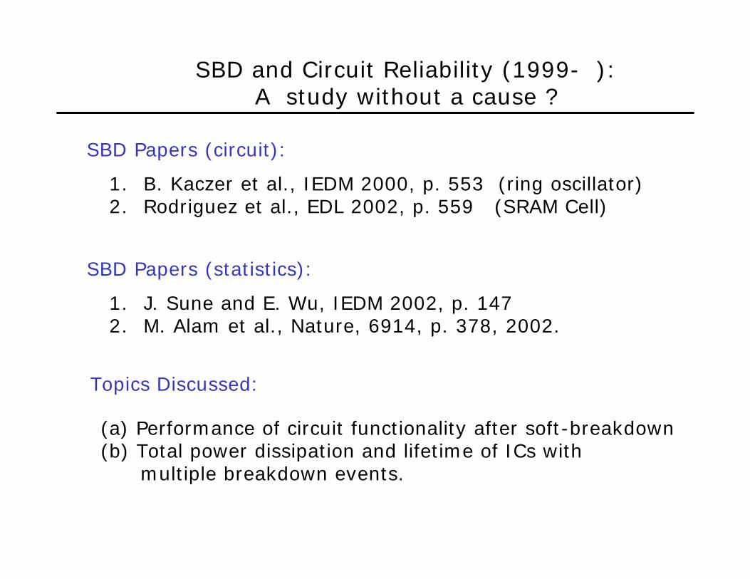
SBD and Circuit Reliability (1999- ):A study without a cause ?
(a) Performance of circuit functionality after soft-breakdown(b) Total power dissipation and lifetime of ICs with
multiple breakdown events.
SBD Papers (circuit):
1. B. Kaczer et al., IEDM 2000, p. 553 (ring oscillator)2. Rodriguez et al., EDL 2002, p. 559 (SRAM Cell)
SBD Papers (statistics):
1. J. Sune and E. Wu, IEDM 2002, p. 1472. M. Alam et al., Nature, 6914, p. 378, 2002.
Topics Discussed:
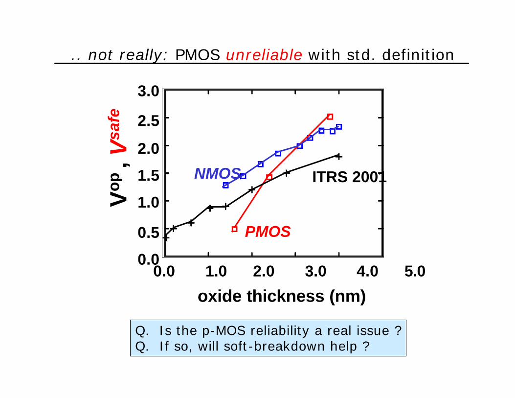
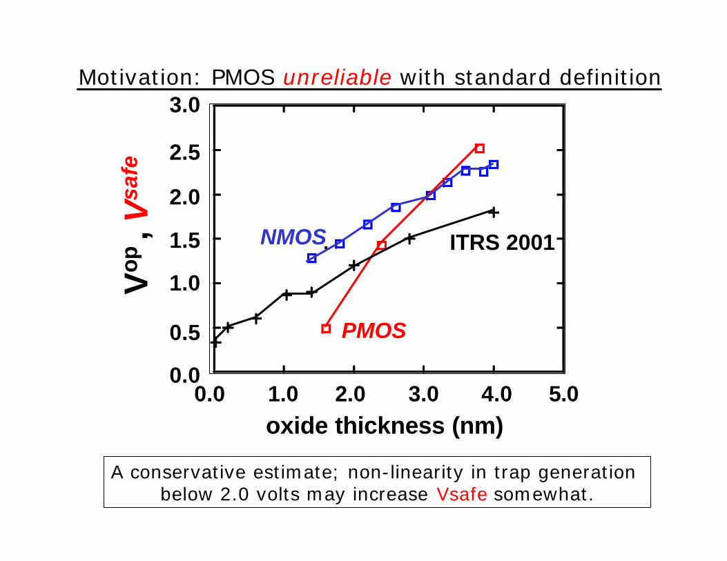
.. not really: PMOS unreliable with std. definition
3.0
2.0
1.5
1.0
0.0
0.5
2.5
0.0 1.0 2.0 3.0 4.0 5.0
oxide thickness (nm)
Vop
, V
safe
NMOS
PMOS
ITRS 2001
Q. Is the p-MOS reliability a real issue ?Q. If so, will soft-breakdown help ?
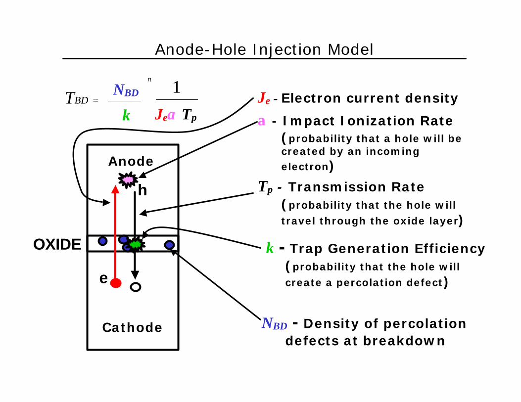
Anode-Hole Injection Model
pe
BDxBD
TJkNT
n
α1
=
Anode
Cathode
e
h
NBD - Density of percolation defects at breakdown
Je - Electron current density
α - Impact Ionization Rate(probability that a hole will be created by an incoming electron)
Tp - Transmission Rate(probability that the hole will
travel through the oxide layer)
k - Trap Generation Efficiency(probability that the hole will
create a percolation defect)
OXIDE
Jeα Tpk
NBD
0 1 2 3 4 5 610-8
10-7
10-6
10-5
10-4
10-3
10-2
10-1
J GA
TE (
Am
ps/
cm2)
VGATE
(Volts)
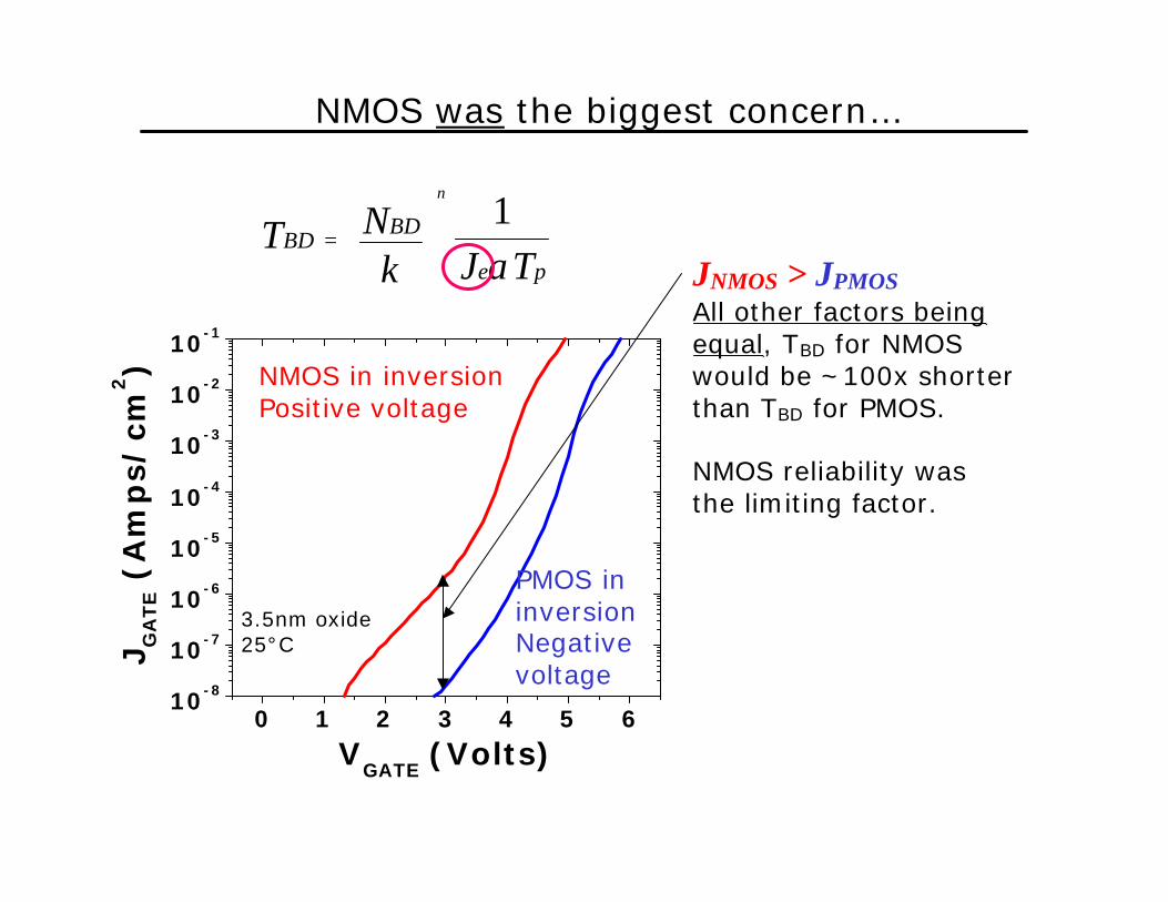
NMOS was the biggest concern…
NMOS in inversionPositive voltage
PMOS in inversionNegative voltage
JNMOS > JPMOSAll other factors being equal, TBD for NMOS would be ~100x shorter than TBD for PMOS.
NMOS reliability was the limiting factor.
pe
BDBD
TJkNT
n
α1
=
3.5nm oxide25°C
1 2 3 4 5 6 710-1210-1110-1010-910-810-710-610-510-410-3
αT p o
r IH
OLE
/I ELE
C
VGATE
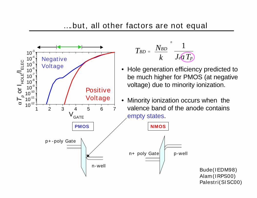
….but, all other factors are not equal
• Hole generation efficiency predicted to be much higher for PMOS (at negative voltage) due to minority ionization.
• Minority ionization occurs when the valence band of the anode contains empty states.
Bude(IEDM98)Alam(IRPS00)Palestri(SISC00)
pe
BDBD
TJkNT
n
α1
=
NegativeVoltage
PositiveVoltage
p+-poly Gate
n-well
PMOS NMOS
p-welln+ poly Gate
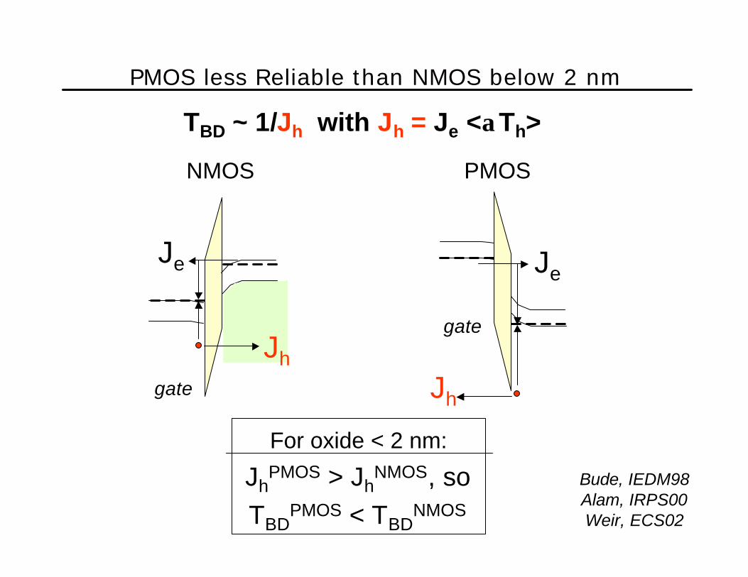
PMOS less Reliable than NMOS below 2 nm
TBD ~ 1/Jh with Jh = Je <αTh>
For oxide < 2 nm:
JhPMOS > Jh
NMOS, so TBD
PMOS < TBDNMOS
Bude, IEDM98Alam, IRPS00Weir, ECS02
Je
Jh
NMOS
gate
Je
Jh
PMOS
gate
-2 -3 -4 -5 -610-410-310-210-1100101102103104105106107108109
PMOS
TBD from SILC TDDB
7.8 dec./V (low voltage region)6 dec./V (all data)
5.2 decs./V
5.5 decs./V
Gate Voltage
Med
ian
TB
D (
sec.
)
3 4 5 6
5.9 dec./V
5.2 dec./V
7.9 dec./V (low voltage region)6.7 dec./V (all data)
NMOS
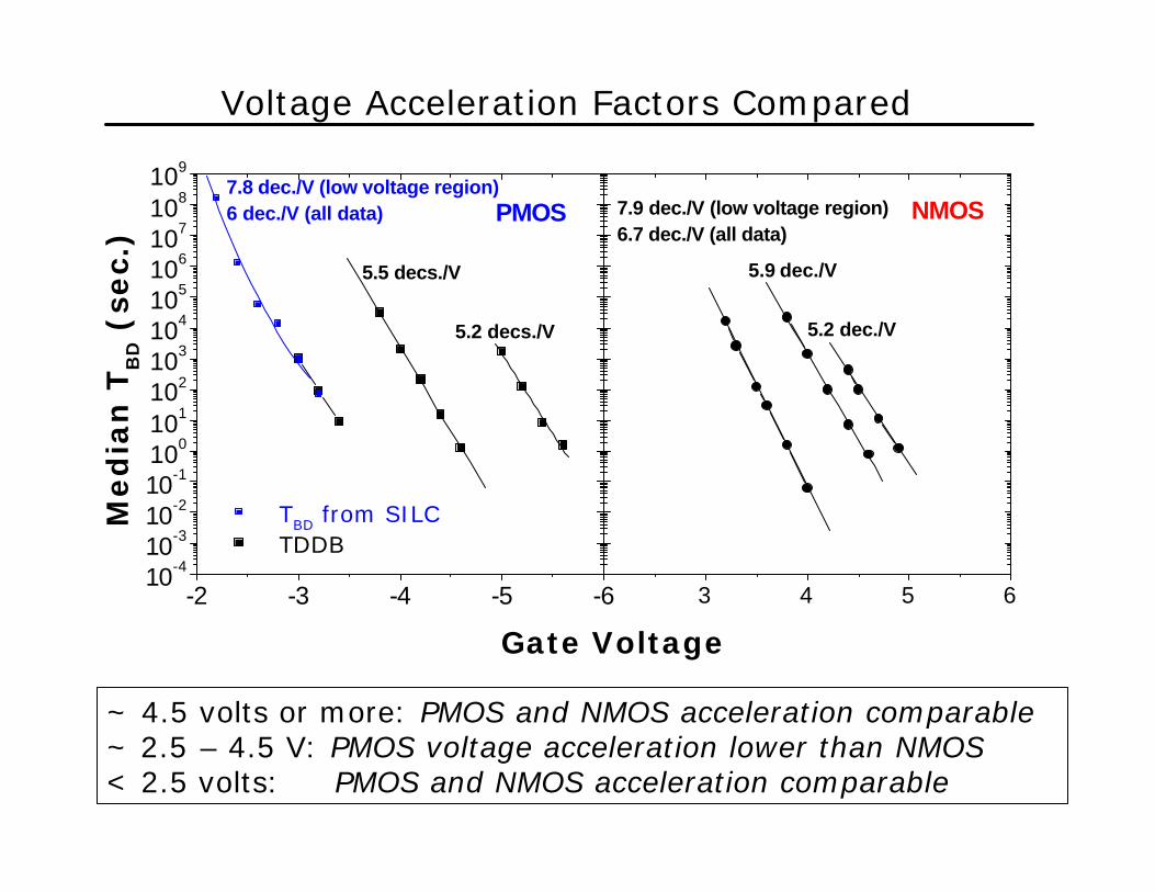
Voltage Acceleration Factors Compared
~ 4.5 volts or more: PMOS and NMOS acceleration comparable~ 2.5 – 4.5 V: PMOS voltage acceleration lower than NMOS< 2.5 volts: PMOS and NMOS acceleration comparable
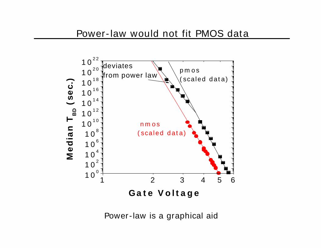
1 2 3 4 5 6100102104106108
1010101210141016101810201022
deviatesfrom power law
pmos(scaled data)
nmos(scaled data)
Gate Voltage
Med
ian
TB
D (
sec.
)
Power-law would not fit PMOS data
Power-law is a graphical aid
Motivation: PMOS unreliable with standard definition3.0
2.0
1.5
1.0
0.0
0.5
2.5
0.0 1.0 2.0 3.0 4.0 5.0oxide thickness (nm)
Vop
, V
safe
NMOS
PMOS
ITRS 2001
A conservative estimate; non-linearity in trap generation below 2.0 volts may increase Vsafe somewhat.
Outline
1. A short history of soft-breakdown
2. Device functionality after soft-breakdown
• Drive current and trans-conductance• Off-current• Threshold voltage shift
3. The digital divide between soft and hard breakdown
4. Lifetime enhancement due to Multiple soft-breakdown
5. Implications for circuit functionality6. Conclusion
GATE
SOURCE
DRAIN
GATE
SOURCE
DRAIN
before
after
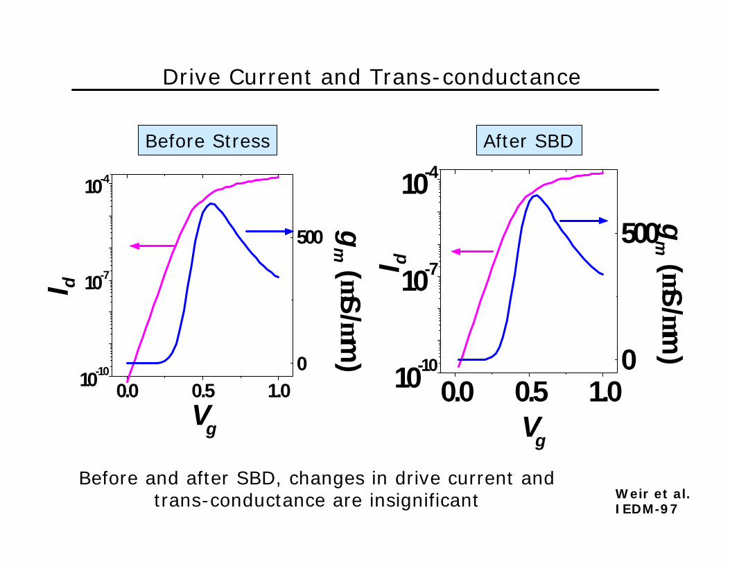
Drive Current and Trans-conductance
0.0 0.5 1.010-10
10-7
10-4
I d
Vg
0
500
gm (µS
/µm)
0.0 0.5 1.010-10
10-7
10-4
Vg
I d0
500
gm (µS
/µm)
Weir et al.IEDM-97
Before and after SBD, changes in drive current andtrans-conductance are insignificant
Before Stress After SBD

-0.5 0.0 0.5 1.0 1.51E-141E-131E-121E-111E-101E-91E-81E-71E-61E-51E-41E-3
Ig Id Is Ib
|Cu
rren
t (A
)|
Vgate
1.7nm. Vg=3.8V (stress), Vd=1.2V (meas)
Off-Current
No GIDL (drain to body current) observed
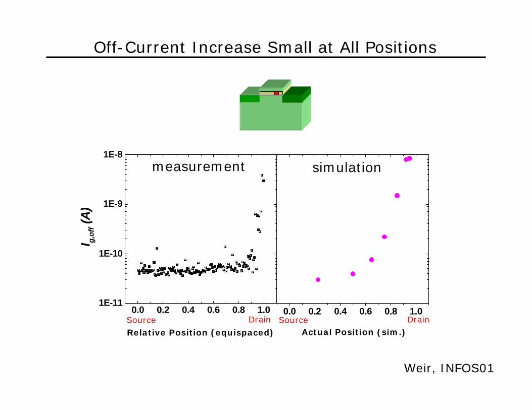
0.0 0.2 0.4 0.6 0.8 1.01E-11
1E-10
1E-9
1E-8
DrainSourceDrainSource
I g,of
f (A
)
Relative Position (equispaced)
0.0 0.2 0.4 0.6 0.8 1.0
Actual Position (sim.)
Off-Current Increase Small at All Positions
measurement simulation
Weir, INFOS01
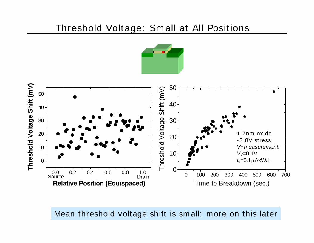
0 100 200 300 400 500 600 7000
10
20
30
40
50
Thr
esho
ld V
olta
ge S
hift
(mV
)
Time to Breakdown (sec.)
0.0 0.2 0.4 0.6 0.8 1.0
0
10
20
30
40
50
DrainSource
Thre
shol
d V
olta
ge S
hift
(mV
)
Relative Position (Equispaced)
1.7nm oxide-3.8V stressVT measurement:Vd=0.1V Id=0.1µAxW/L
Threshold Voltage: Small at All Positions
Mean threshold voltage shift is small: more on this later
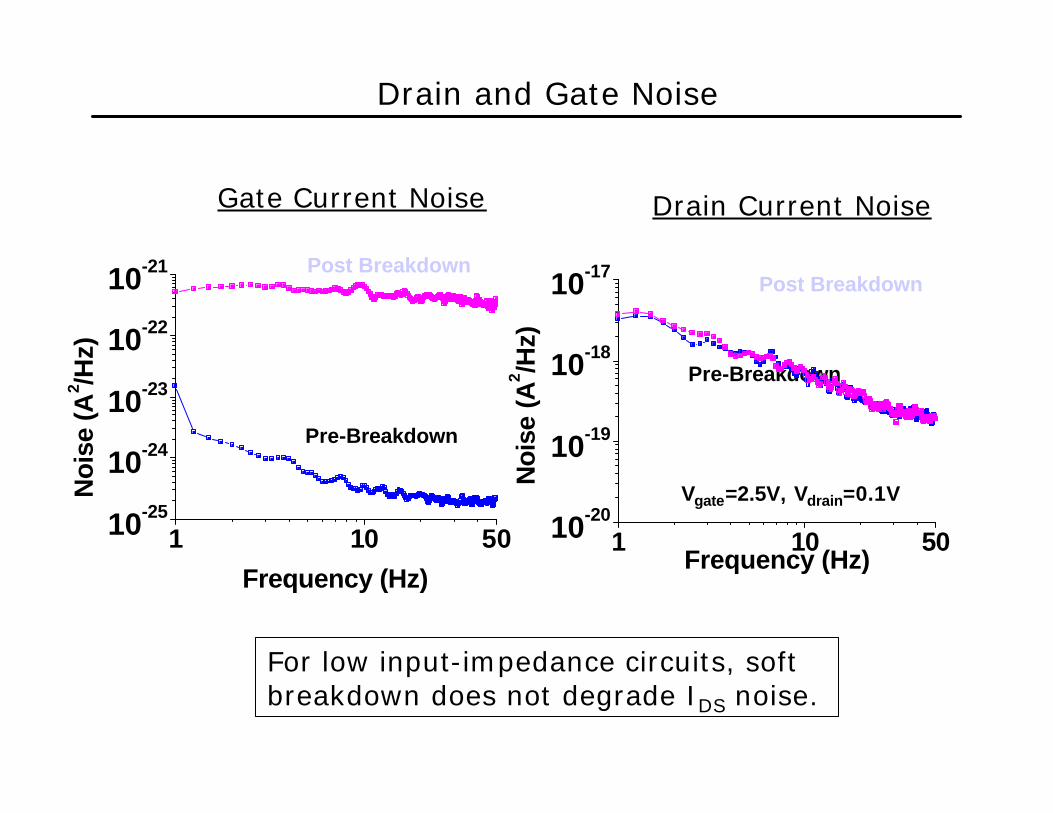
For low input-impedance circuits, soft breakdown does not degrade IDS noise.
Gate Current Noise Drain Current Noise
Vgate=2.5V, Vdrain=0.1V
Pre-Breakdown
Post Breakdown
Pre-Breakdown
Post Breakdown
1 10 5010-25
10-24
10-23
10-22
10-21
Noi
se (A
2 /Hz)
Frequency (Hz)1 10 5010-20
10-19
10-18
10-17
Noi
se (
A2 /H
z)Frequency (Hz)
Drain and Gate Noise
Outline
1. A short history of soft-breakdown2. Device functionality after soft-breakdown
3. The digital divide between soft and hard breakdown
• A theory of hard and hard breakdown• Area, thickness, and voltage dependence
4. Lifetime enhancement due to Multiple soft-breakdown
5. Implications for circuit functionality6. Conclusion
How do we show that the excellent properties of few soft-broken transistors just discussed will apply to
hundreds of millions of transistors in an IC ?
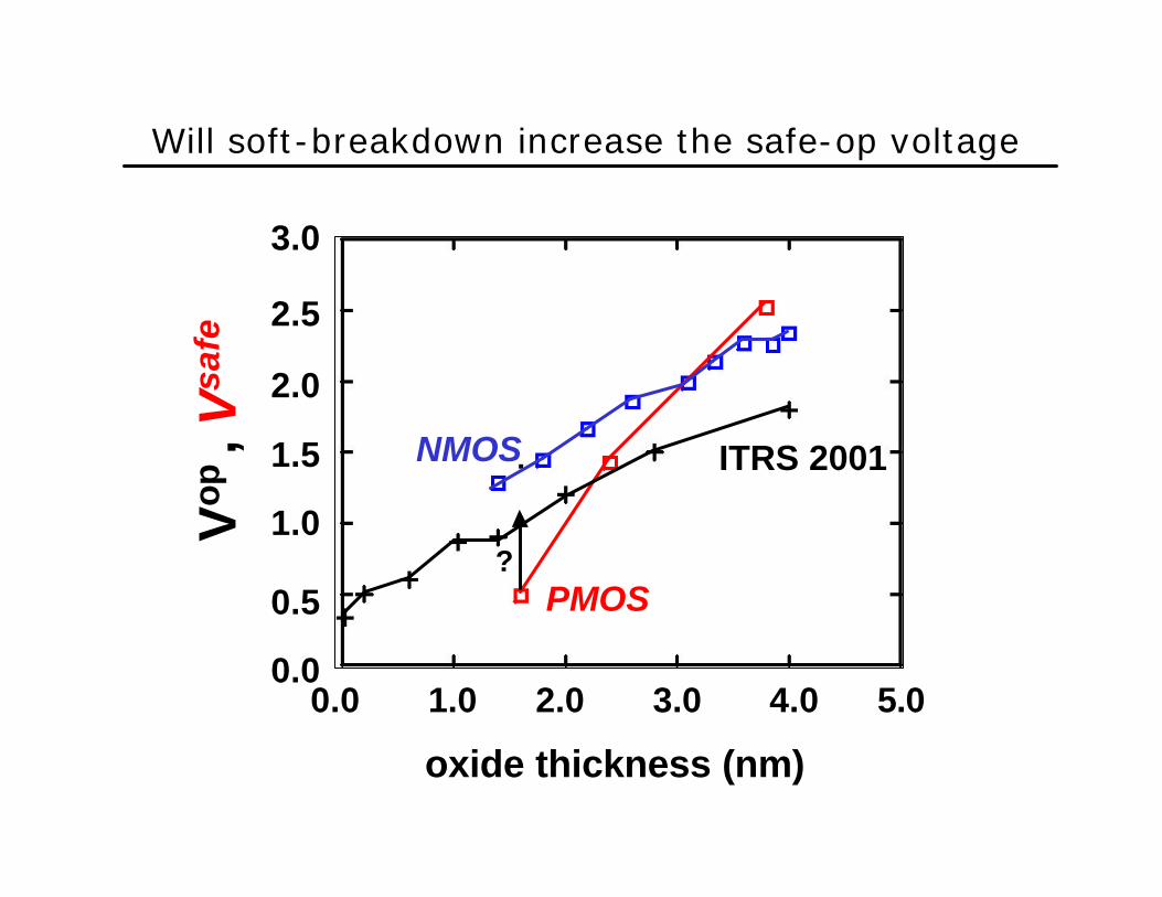
Will soft-breakdown increase the safe-op voltage
3.0
2.0
1.5
1.0
0.0
0.5
2.5
0.0 1.0 2.0 3.0 4.0 5.0
oxide thickness (nm)
Vop
, V
safe
NMOS
PMOS
ITRS 2001
?
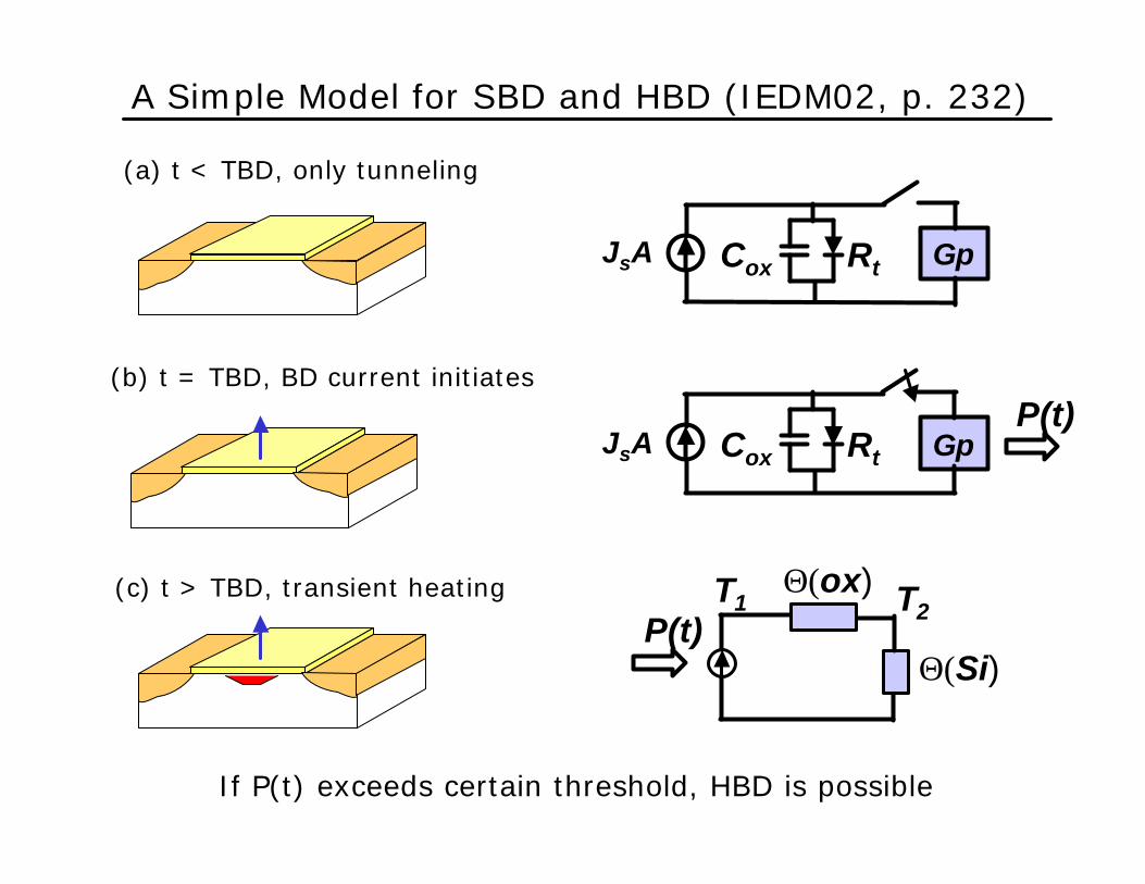
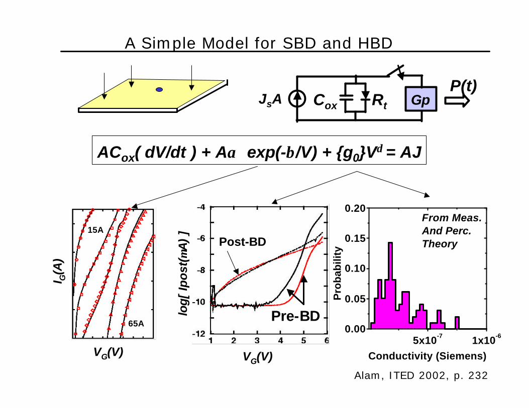
A Simple Model for SBD and HBD (IEDM02, p. 232)
GpRtCoxJsAP(t)
(a) t < TBD, only tunneling
(b) t = TBD, BD current initiates
(c) t > TBD, transient heating Θ(ox)
Θ(Si)
T1 T2
GpRtCoxJsA
P(t)
If P(t) exceeds certain threshold, HBD is possible
A Simple Model for SBD and HBD
VG(V)
I G(A
)
VG(V)
log[
Ipo
st(µ
A)
]
ACox( dV/dt ) + Aα exp(-β/V) + {g0}Vδ = AJ
GpRtCoxJsAP(t)
5x10⁻⁷ 1x10-60.00
0.05
0.10
0.15
0.20
Pro
bab
ility
Conductivity (Siemens)
Post-BD
Pre-BD
From Meas.And Perc. Theory
15A
65A
Alam, ITED 2002, p. 232
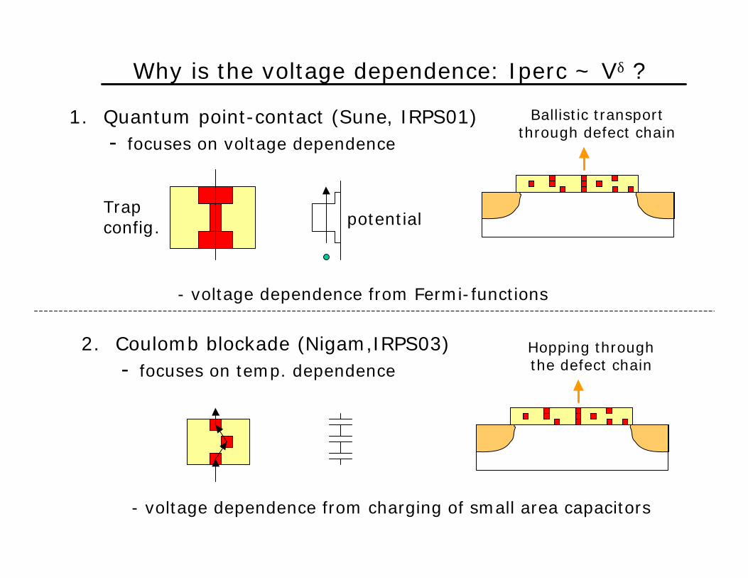
Why is the voltage dependence: Iperc ~ Vδ ?
1. Quantum point-contact (Sune, IRPS01)- focuses on voltage dependence
Ballistic transportthrough defect chain
2. Coulomb blockade (Nigam,IRPS03)- focuses on temp. dependence
Hopping throughthe defect chain
Trapconfig. potential
- voltage dependence from Fermi-functions
- voltage dependence from charging of small area capacitors
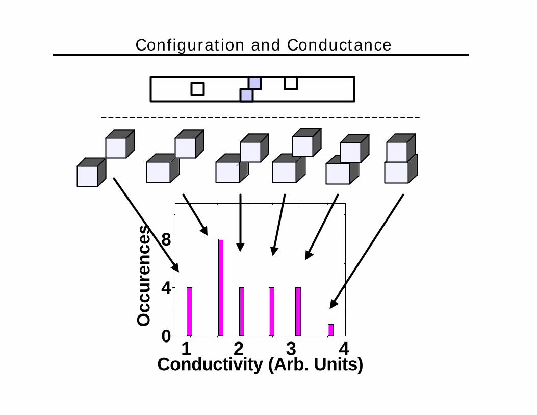
Configuration and Conductance
0.005 0.010 0.0150
4
8
Occ
ure
nce
s
Conductivity (Arb. Units)1 2 3 4
Statistical distribution of Gp
•Weakly thickness dependent• Gmax/Gmin= 5 -105x10-7 1x10⁻⁶
0.0
0.2
0.4 Pro
bab
ility
Conductivity (Siemens)
0.0
0.2
0.4
2 nm1.7 nm
1.5 nm
Meas
3a0
2.2a0 2a0
Sim.(arb. units)
Sample 1
Sample 2
Sample n
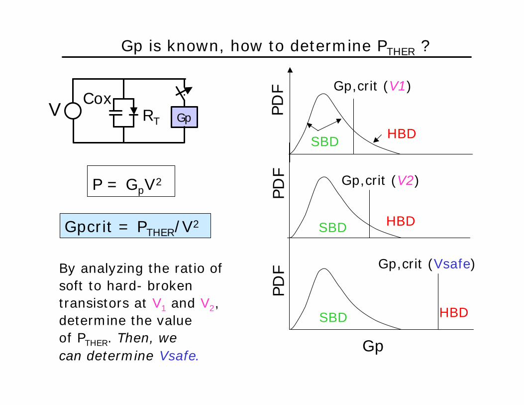
Gp is known, how to determine PTHER ?
GpRT
CoxV
P = GpV2
Gpcrit = PTHER/V2
Gp,crit (V1)
PD
F
SBD HBD
By analyzing the ratio of soft to hard- broken transistors at V1 and V2, determine the value of PTHER. Then, we can determine Vsafe.
Gp
Gp,crit (Vsafe)PD
F
SBD HBD
Gp,crit (V2)
PD
F
SBD HBD
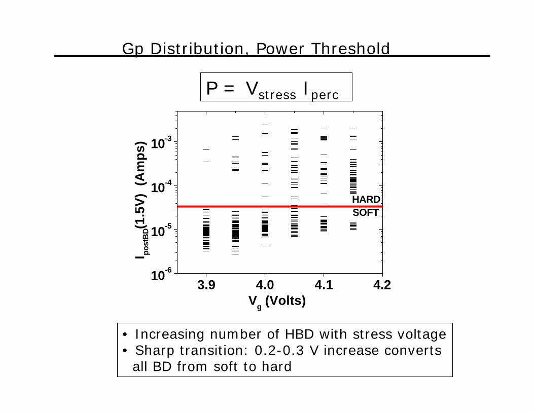
Gp Distribution, Power Threshold
3.9 4.0 4.1 4.210-6
10-5
10-4
10-3
HARDSOFT
I post
BD(1
.5V
) (
Am
ps)
Vg (Volts)
P = Vstress Iperc
• Increasing number of HBD with stress voltage• Sharp transition: 0.2-0.3 V increase converts
all BD from soft to hard
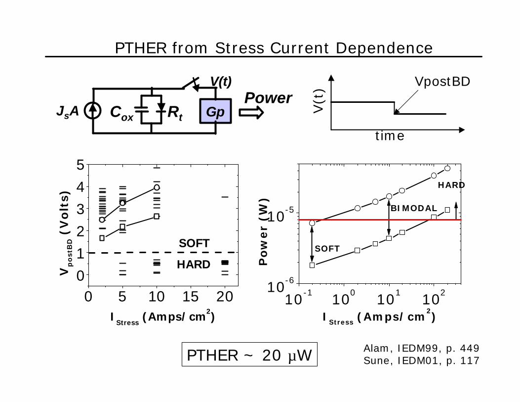
PTHER from Stress Current Dependence
0 5 10 15 20012345
HARD
SOFT
Vp
ost
BD (
Vo
lts)
IStress
(Amps/cm2)10
-110
010
110
210-6
10-5
HARD
BIMODAL
SOFT
Pow
er
(W)
IStress (Amps/cm2)
time
V(t
) VpostBD
PTHER ~ 20 µW Alam, IEDM99, p. 449 Sune, IEDM01, p. 117
GpRtCoxJsAPower
V(t)
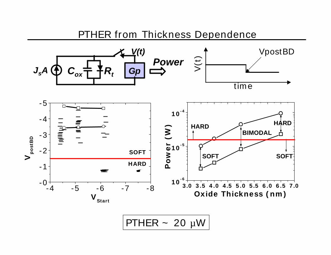
PTHER from Thickness Dependence
PTHER ~ 20 µW
3.0 3.5 4.0 4.5 5.0 5.5 6.0 6.5 7.010-6
10-5
10-4
HARD
BIMODAL
SOFT SOFT
HARD
Pow
er
(W)
Oxide Thickness (nm)-4 -5 -6 -7 -8
-0
-1
-2
-3
-4
-5
HARD
SOFT
Vp
ost
BD
VStart
time
V(t
) VpostBD
GpRtCoxJsAPower
V(t)
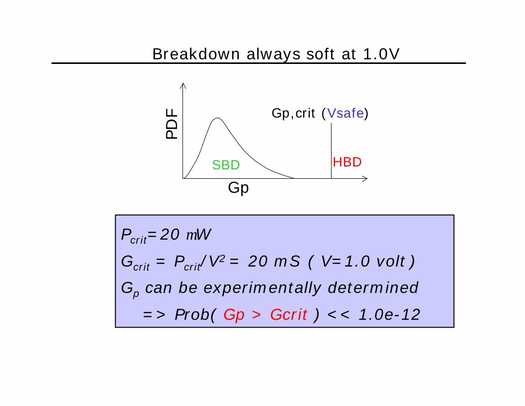
Breakdown always soft at 1.0V
Pcrit=20 µW
Gcrit = Pcrit/V2 = 20 mS ( V=1.0 volt )
Gp can be experimentally determined
=> Prob( Gp > Gcrit ) << 1.0e-12
Gp
Gp,crit (Vsafe)
PD
FSBD HBD
Outline
1. A short history of soft-breakdown2. Device functionality after soft-breakdown3. The digital divide between soft and
hard breakdown
4. Lifetime enhancement due to Multiple soft-breakdown
• Understanding spatial and temporal correlation• Techniques of making projections
5. Implications for circuit functionality6. Conclusion
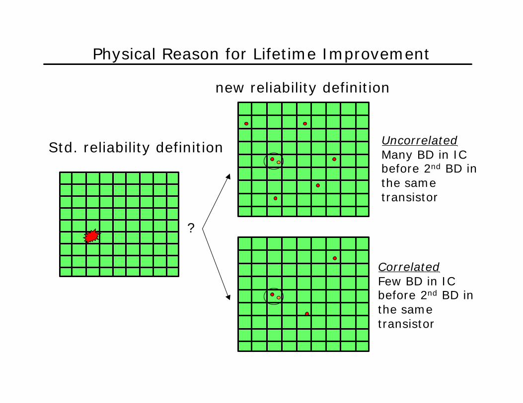
Physical Reason for Lifetime Improvement
Std. reliability definition
new reliability definition
?
UncorrelatedMany BD in ICbefore 2nd BD in the same transistor
CorrelatedFew BD in ICbefore 2nd BD in the same transistor
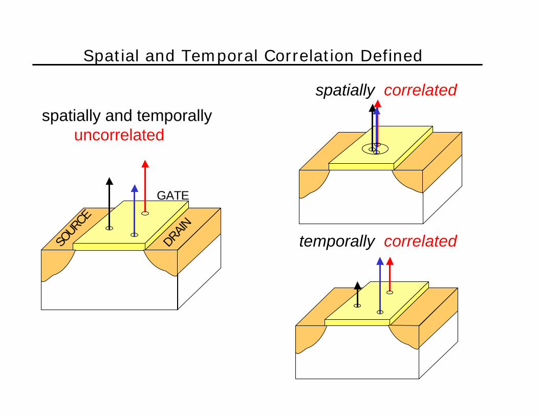
Spatial and Temporal Correlation Defined
GATE
SOURCE
DRAIN
spatially correlated
spatially and temporally uncorrelated
temporally correlated
Loc of a breakdown spot: x = Id / ( Is + Id )Time of breakdown: T1, T2 , T3 , etc.
How to Determine the Statistics of Trap Generation
GATE
SOURCE
DRAINIs Id
1st SBD
2nd SBD
3rd SBD
log (Time)G
ate
Cu
rren
t (m
A) 0.6
0.4
0.2
0.00 1 2 3 4
Degraeve, IRPS01
gate
perc
ds
d
perc
percs
L
x
JJJ
x
nDJ
BAxndx
ndD
J
nedxdn
DJ
=+
=
+=
=
=•∇
+=
0
0
2
2
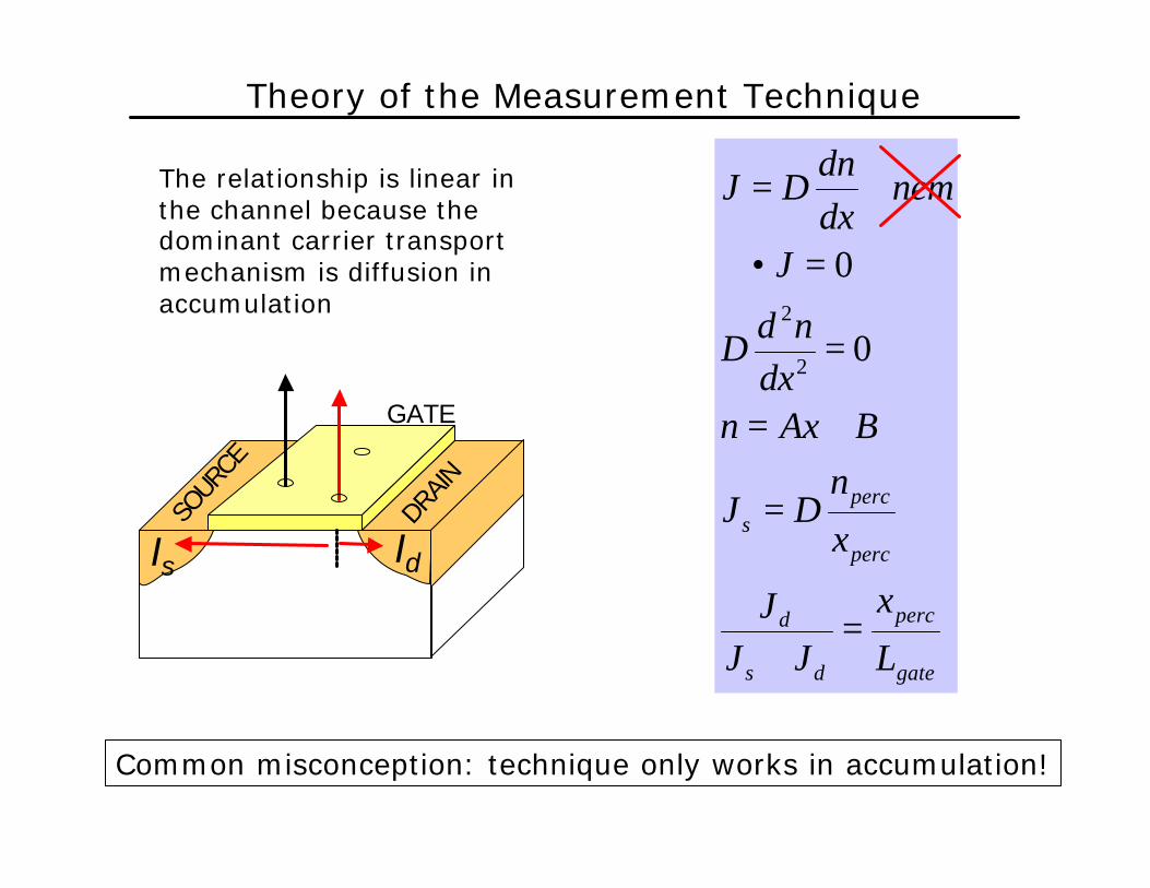
µThe relationship is linear in the channel because the dominant carrier transport mechanism is diffusion in accumulation
Theory of the Measurement Technique
GATE
SOURCE
DRAIN
Is Id
Common misconception: technique only works in accumulation!
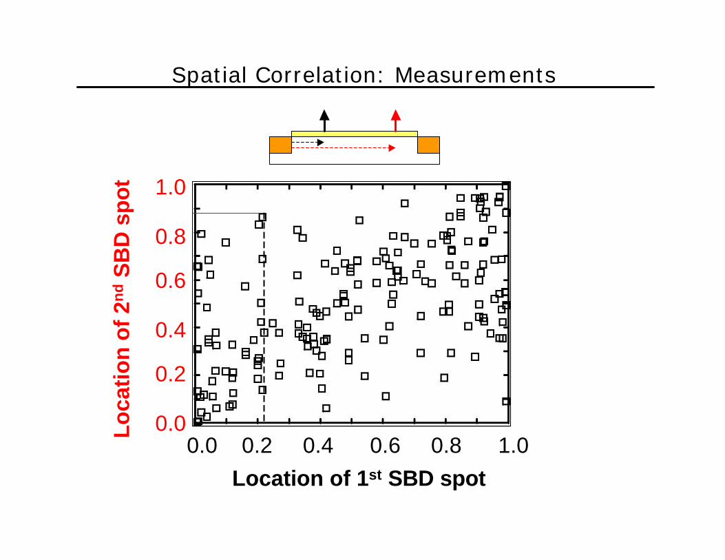
Spatial Correlation: Measurements
Location of 1st SBD spot
Lo
cati
on
of
2nd
SB
D s
pot
0.0 0.2 0.4 0.6 0.8 1.0
1.0
0.6
0.8
0.0
0.4
0.2
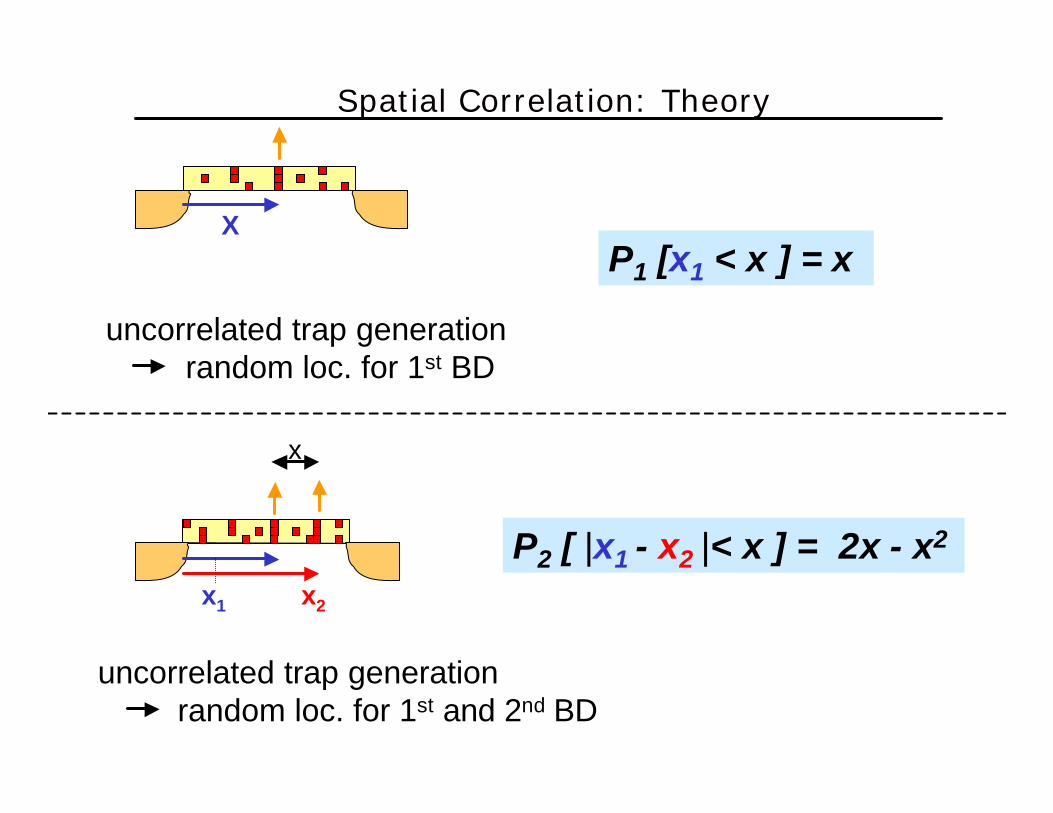
Spatial Correlation: Theory
P1 [x1 < x ] = x
P2 [ |x1 - x2 |< x ] = 2x - x2
X
x1 x2
uncorrelated trap generation random loc. for 1st and 2nd BD
uncorrelated trap generation random loc. for 1st BD
x
Spatial Correlation: Analysis
Trap generation is spatially uncorrelated (essentially)!
0.0 0.2 0.4 0.6 0.8 1.0 0.0 0.2 0.4 0.6 0.8 1.0
1.0
0.8
0.6
0.4
0.2
0.0
loc of 1st SBD distance betn 1st and 2nd SBD
Cu
mu
lativ
e P
DF
Cu
mu
lativ
e P
DF
P1 = x P2 = 2x - x2
0.2 0.4 0.6
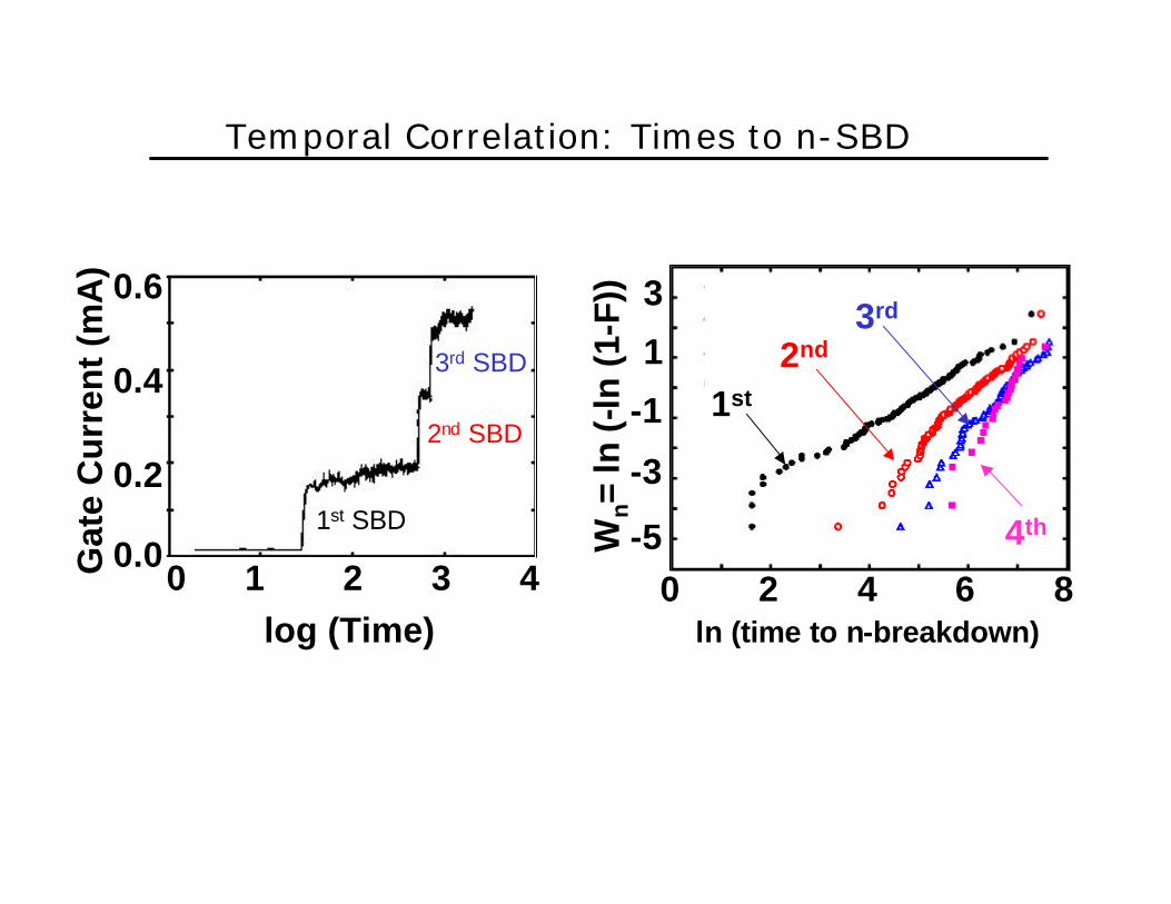
Temporal Correlation: Times to n-SBD
1st SBD
2nd SBD
3rd SBD
log (Time)
Gat
e C
urr
ent
(mA
) 0.6
0.4
0.2
0.00 1 2 3 4
3
1
-1
-3
-5Wn=
ln (-
ln (
1-F)
)ln (time to n-breakdown)
0 2 4 6 8
1st
2nd3rd
4th
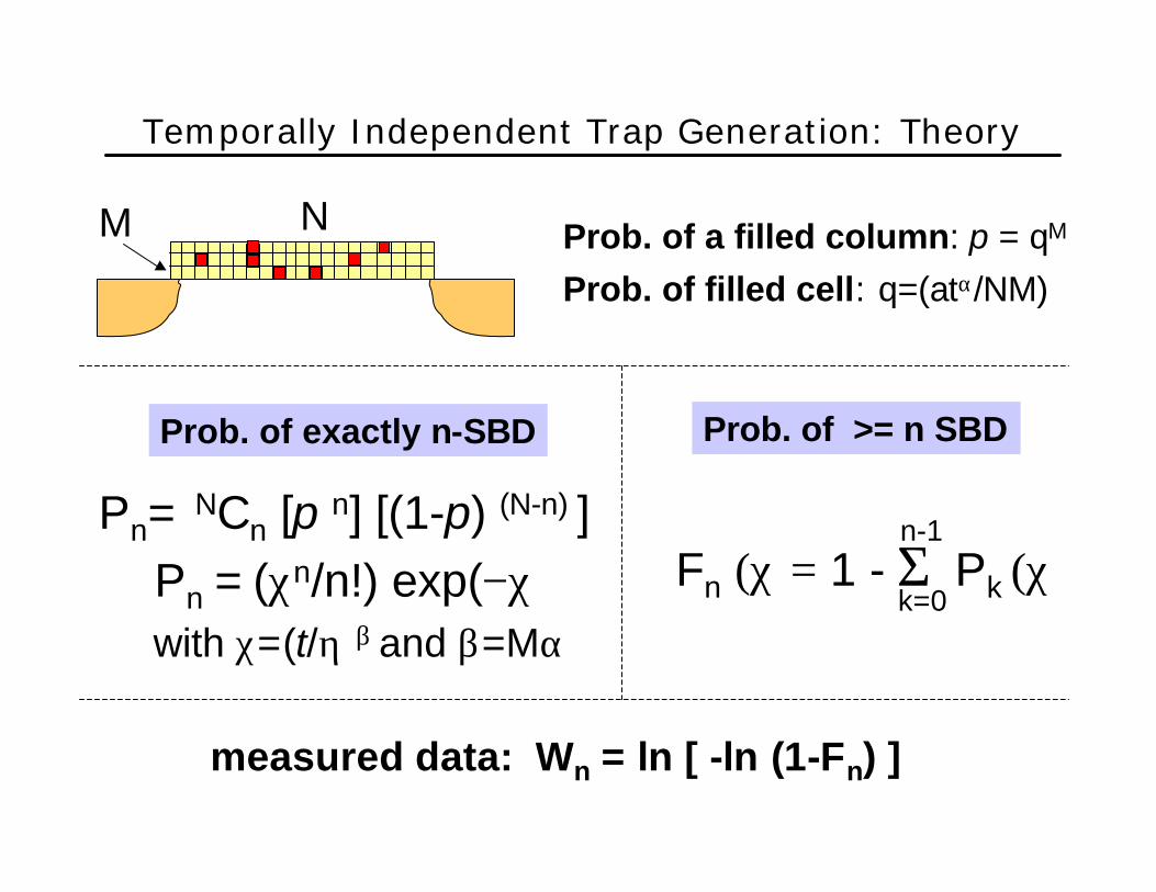
Temporally Independent Trap Generation: Theory
NM
Pn= NCn [p n] [(1-p) (N-n) ]Pn = (χn/n!) exp(−χ)with χ=(t/η)β and β=Mα
Fn (χ)= 1 - Σ Pk (χ)
Prob. of exactly n-SBD Prob. of >= n SBD
k=0
n-1
Prob. of a filled column: p = qM
Prob. of filled cell: q=(atα/NM)
measured data: Wn = ln [ -ln (1-Fn) ]
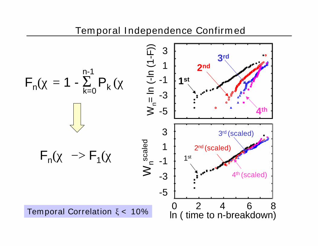
Temporal Independence Confirmed
0 2 4 6 8
3
1-1
-3
-5
3
1-1
-3
-5
Wn=
ln (
-ln (
1-F)
)W
nscal
ed
ln ( time to n-breakdown)
Fn(χ)= 1 - Σ Pk (χ)k=0
n-1
Fn(χ) −> F1(χ)
1st
2nd3rd
4th
1st
2nd (scaled)
3rd (scaled)
4th (scaled)
Temporal Correlation ξ < 10%
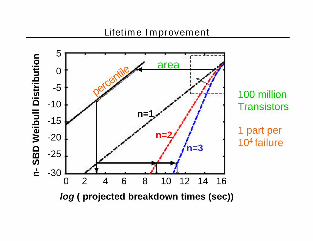
Lifetime Improvement
0 2 4 6 8 10 12 14 16
n-S
BD
Wei
bu
ll D
istr
ibu
tion
area
perce
ntile
n=1
n=2n=3
5
0
-5
-10
-15
-20
-25
-30
log ( projected breakdown times (sec))
100 millionTransistors
1 part per 104 failure
Lifetime Improvement
(Tn (ξ=0) /T1)β = (n/e)(2πn)1/2n /Fn(1-1/n)
0
4
-6 -4 0log10 [Failure Fraction]
Rel
ativ
e Im
pro
vem
ent
log10 (
Tn/T
1)β
-2
1
2
3
n=1
n=2
n=3
n=4 Theory
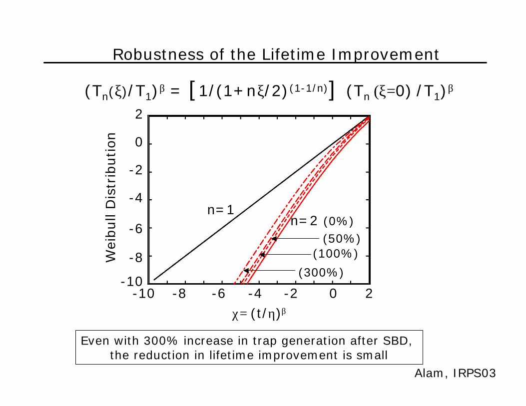
Robustness of the Lifetime Improvement
(Tn(ξ)/T1)β = [1/(1+nξ/2)(1-1/n)] (Tn (ξ=0) /T1)β
-10 20-2
2
-10
Wei
bull
Dis
trib
ution
χ= (t/η)β
n=1n=2 (0%)
(50%)(100%)
(300%)
-4-6-8
-8
-6
-4
-2
0
Even with 300% increase in trap generation after SBD, the reduction in lifetime improvement is small
Alam, IRPS03
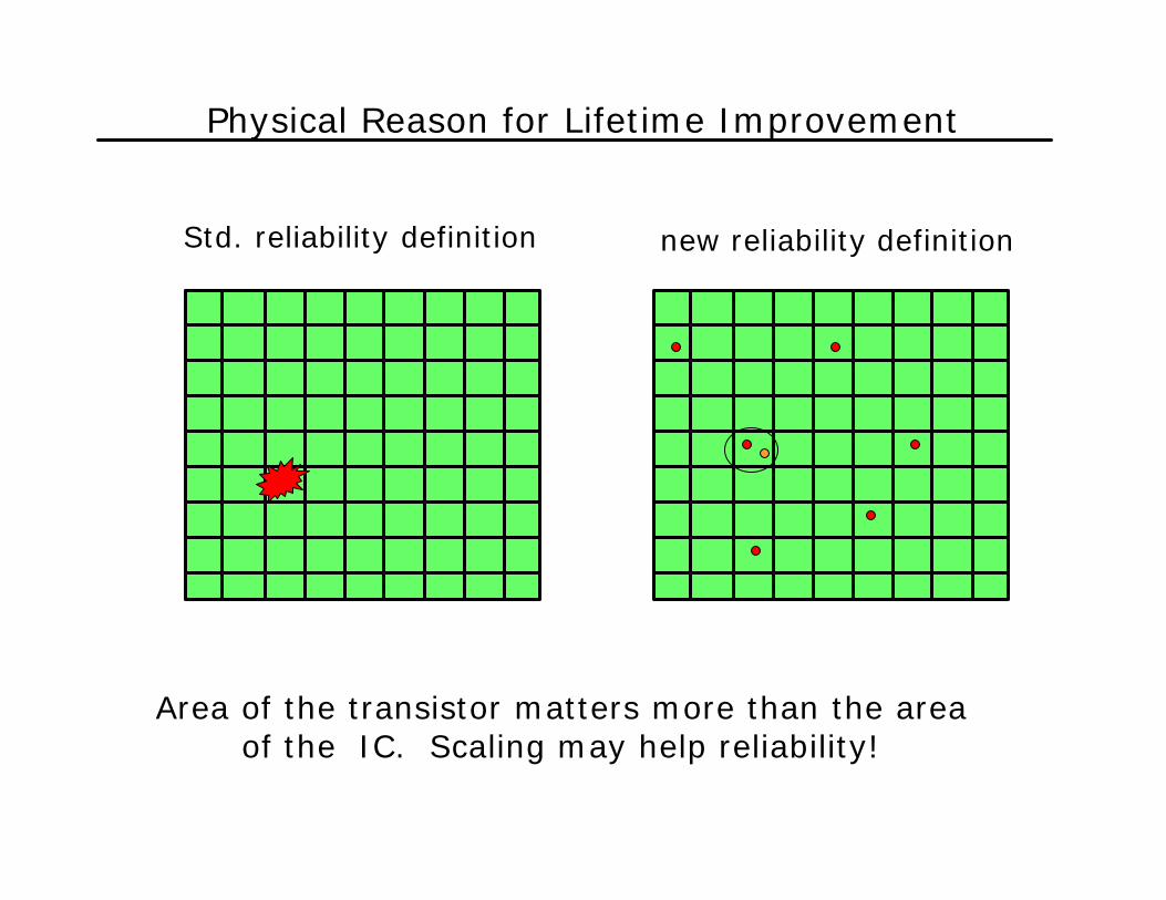
Physical Reason for Lifetime Improvement
Area of the transistor matters more than the areaof the IC. Scaling may help reliability!
Std. reliability definition new reliability definition
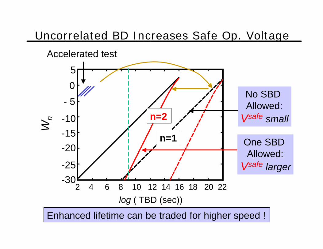
Uncorrelated BD Increases Safe Op. VoltageW
n
n=1
n=2
5
0
-10-15-20
-25-30
log ( TBD (sec))
- 5
Enhanced lifetime can be traded for higher speed !
2 4 6 8 10 12 14 16 18 20 22
No SBD Allowed:
Vsafe small
One SBD Allowed:
Vsafe larger
Accelerated test
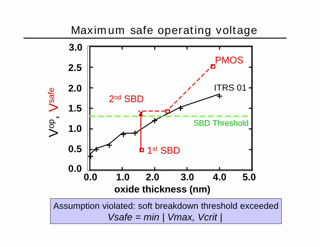
Maximum safe operating voltage
Assumption violated: soft breakdown threshold exceededVsafe = min | Vmax, Vcrit |
3.0
2.0
1.5
1.0
0.0
0.5
2.5
0.0 1.0 2.0 3.0 4.0 5.0oxide thickness (nm)
Vop
, Vsa
fePMOS
ITRS 01
SBD Threshold
1st SBD
2nd SBD
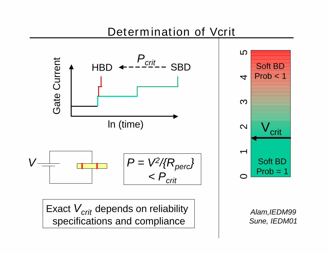
Determination of Vcrit
ln (time)
Gat
e C
urre
nt SBDHBD
0
1
2
3
4
5
Soft BDProb < 1
Soft BDProb = 1
Vcrit
Exact Vcrit depends on reliability specifications and compliance
V P = V2/{Rperc} < Pcrit
Alam,IEDM99Sune, IEDM01
Pcrit
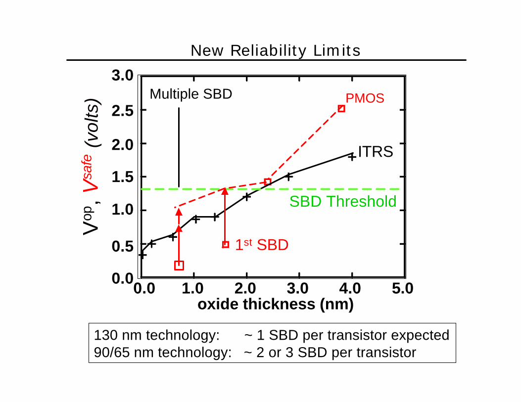
New Reliability Limits
130 nm technology: ~ 1 SBD per transistor expected90/65 nm technology: ~ 2 or 3 SBD per transistor
3.0
2.0
1.5
1.0
0.0
0.5
2.5
0.0 1.0 2.0 3.0 4.0 5.0oxide thickness (nm)
Vop
, Vsa
fe(v
olts
) PMOS
ITRS
Multiple SBD
SBD Threshold
1st SBD
Outline
1. A short history of soft-breakdown2. Device functionality after soft-breakdown3. The digital divide between soft and hard breakdown4. Lifetime enhancement due to Multiple soft breakdown
5. Implications for circuit functionality
• Leakage current• Threshold voltage shift• Static Circuits• Dynamic Circuits
6. Conclusions
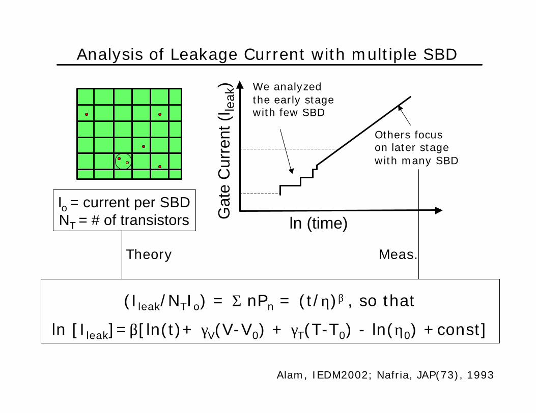
Analysis of Leakage Current with multiple SBD
(Ileak/NTIo) = Σ nPn = (t/η)β , so that
ln [Ileak]=β[ln(t)+ γV(V-V0) + γT(T-T0) - ln(η0) +const]
Io = current per SBDNT = # of transistors ln (time)G
ate
Cur
rent
(I le
ak) We analyzed
the early stage with few SBD
Others focuson later stagewith many SBD
Alam, IEDM2002; Nafria, JAP(73), 1993
Theory Meas.
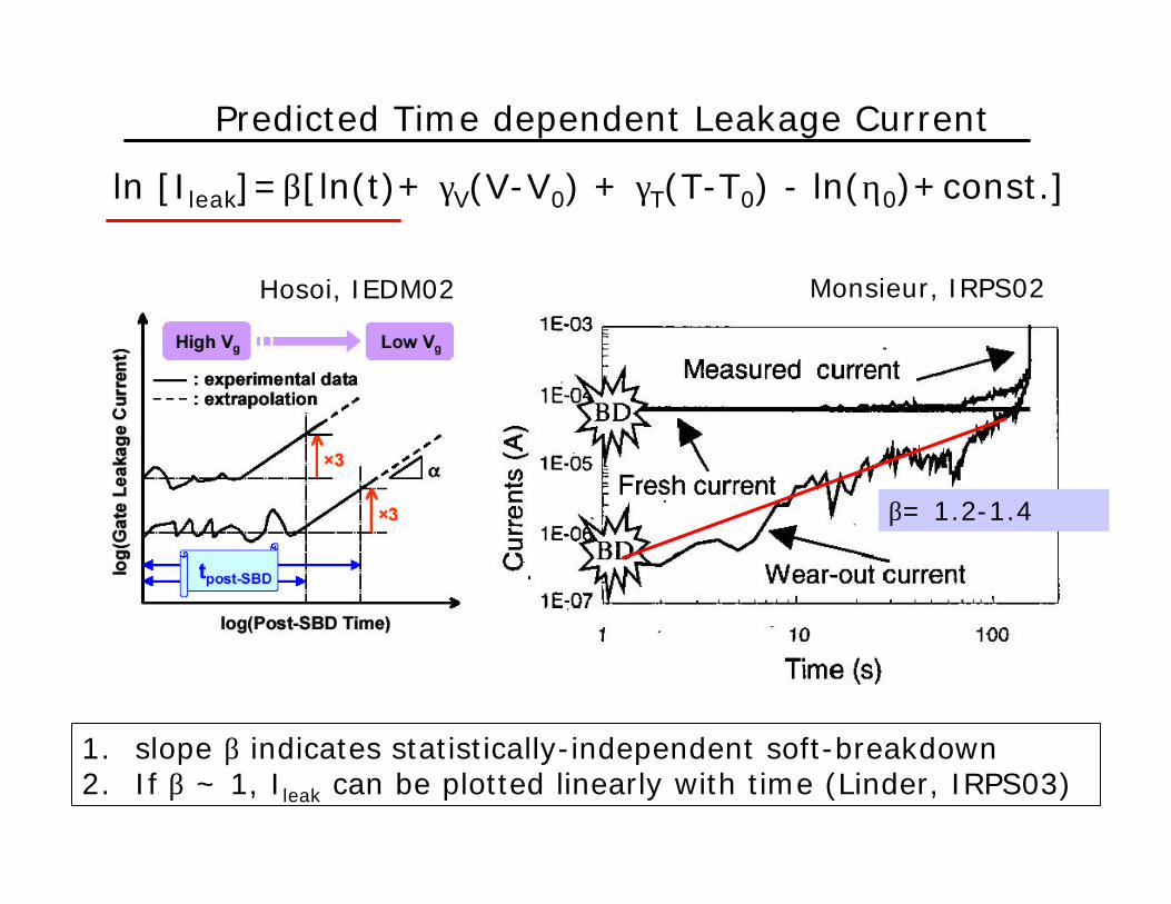
Predicted Time dependent Leakage Current
1. slope β indicates statistically-independent soft-breakdown2. If β ~ 1, Ileak can be plotted linearly with time (Linder, IRPS03)
ln [Ileak]=β[ln(t)+ γV(V-V0) + γT(T-T0) - ln(η0)+const.]
β= 1.2-1.4
Hosoi, IEDM02 Monsieur, IRPS02
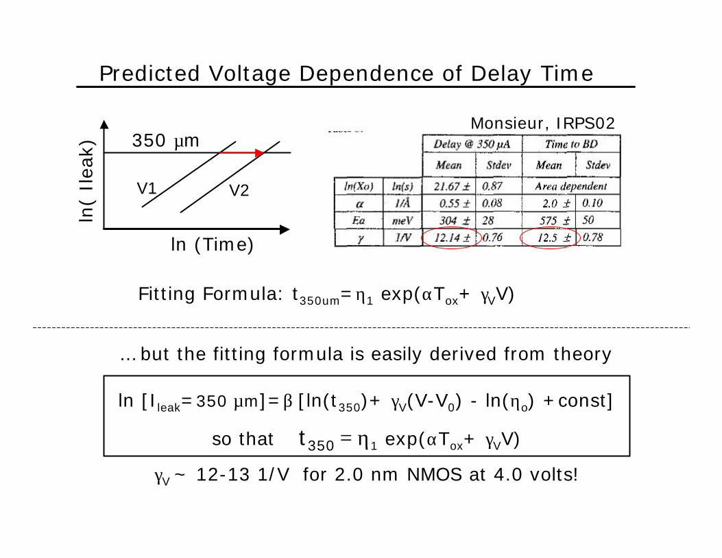
Predicted Voltage Dependence of Delay Time
Fitting Formula: t350um=η1 exp(αTox+ γVV)
ln [Ileak=350 µm]=β [ln(t350)+ γV(V-V0) - ln(ηo) +const]
so that t350 = η1 exp(αTox+ γVV)
… but the fitting formula is easily derived from theory
γV ~ 12-13 1/V for 2.0 nm NMOS at 4.0 volts!
ln(
Ilea
k)
ln (Time)
350 µm
V1 V2
Monsieur, IRPS02
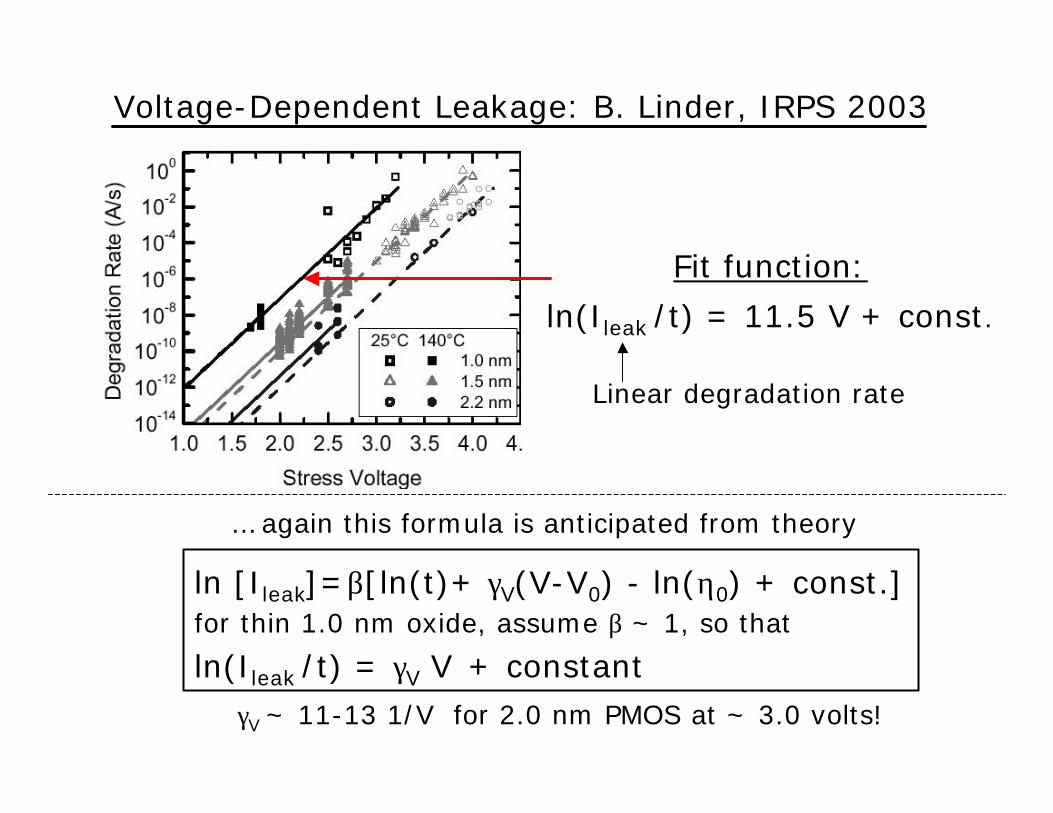
Voltage-Dependent Leakage: B. Linder, IRPS 2003
ln [Ileak]=β[ln(t)+ γV(V-V0) - ln(η0) + const.] for thin 1.0 nm oxide, assume β ~ 1, so that
ln(Ileak /t) = γV V + constant
Fit function:
ln(Ileak /t) = 11.5 V + const.
… again this formula is anticipated from theory
γV ~ 11-13 1/V for 2.0 nm PMOS at ~ 3.0 volts!
Linear degradation rate
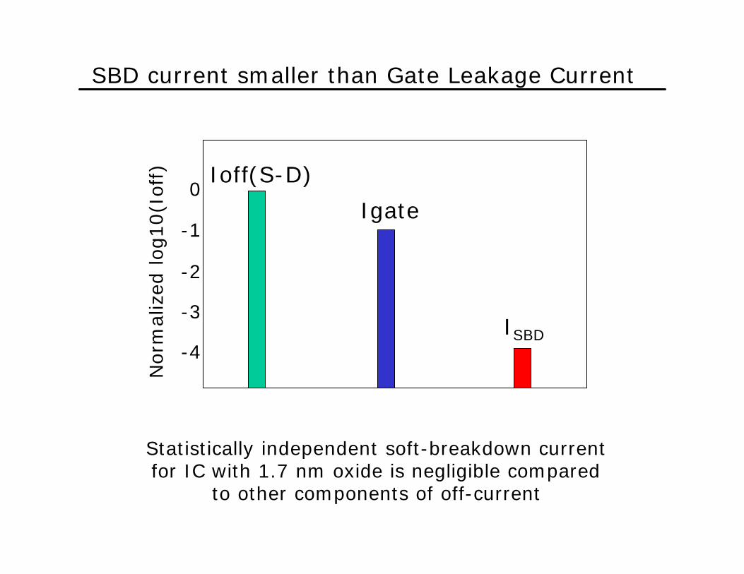
SBD current smaller than Gate Leakage Current
Ioff(S-D)
Igate
ISBD
0
-1
-4
-2
-3
Nor
mal
ized
log
10(I
off)
Statistically independent soft-breakdown current for IC with 1.7 nm oxide is negligible compared
to other components of off-current
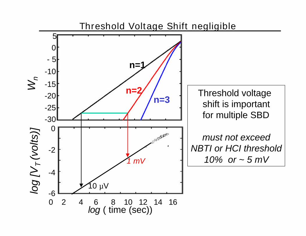
Threshold Voltage Shift negligibleW
n
n=1
n=2n=3
50
-10
-15-20
-25-30
log ( time (sec))
- 5
Threshold voltage shift is importantfor multiple SBD
must not exceed NBTI or HCI threshold
10% or ~ 5 mV
log
[VT
(vol
ts)]
0 2 4 6 8 10 12 14 16-6
-4
-2
0
1 mV
10 µV
.
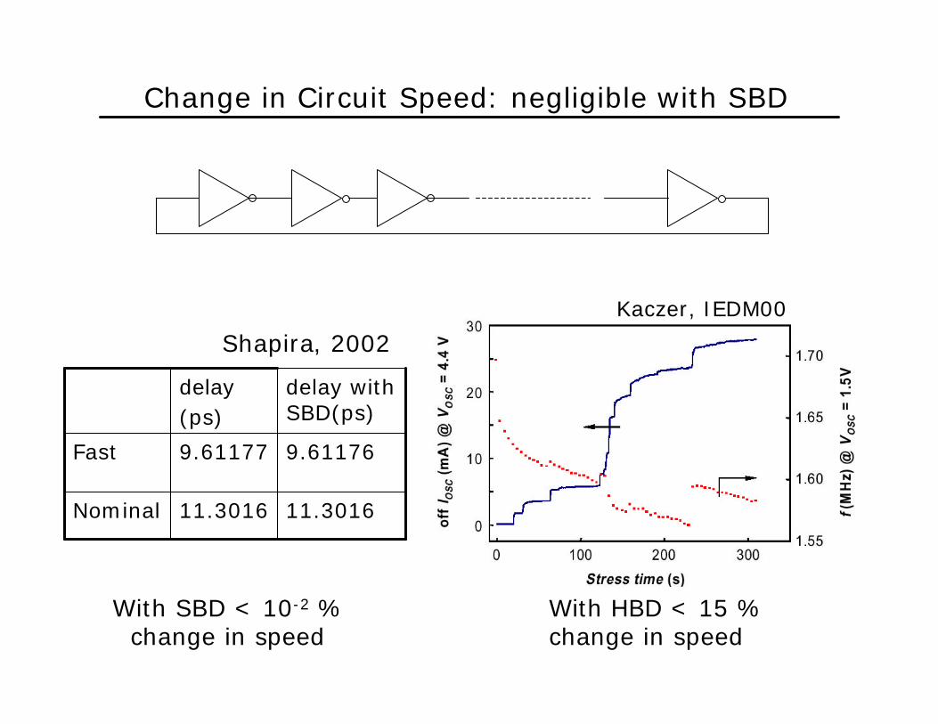
Change in Circuit Speed: negligible with SBD
With HBD < 15 % change in speed
With SBD < 10-2 % change in speed
Kaczer, IEDM00
11.301611.3016Nominal
9.611769.61177Fast
delay with SBD(ps)
delay(ps)
Shapira, 2002
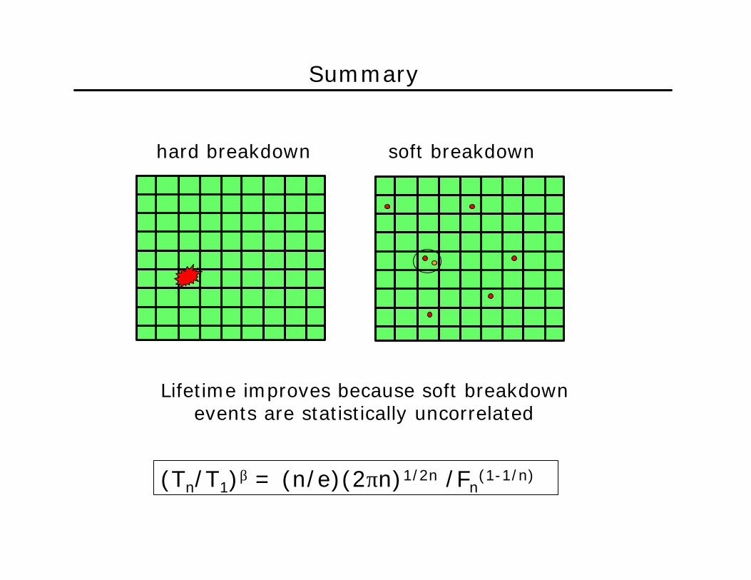
Summary
Lifetime improves because soft breakdownevents are statistically uncorrelated
hard breakdown soft breakdown
(Tn/T1)β = (n/e)(2πn)1/2n /Fn(1-1/n)
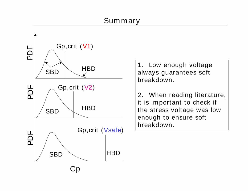
Gp,crit (V1)
PD
F
SBD HBD
Gp
Gp,crit (Vsafe)
PD
F
SBD HBD
Gp,crit (V2)
PD
F
SBD HBD
Summary
1. Low enough voltagealways guarantees softbreakdown.
2. When reading literature,it is important to check if the stress voltage was lowenough to ensure softbreakdown.
Summary
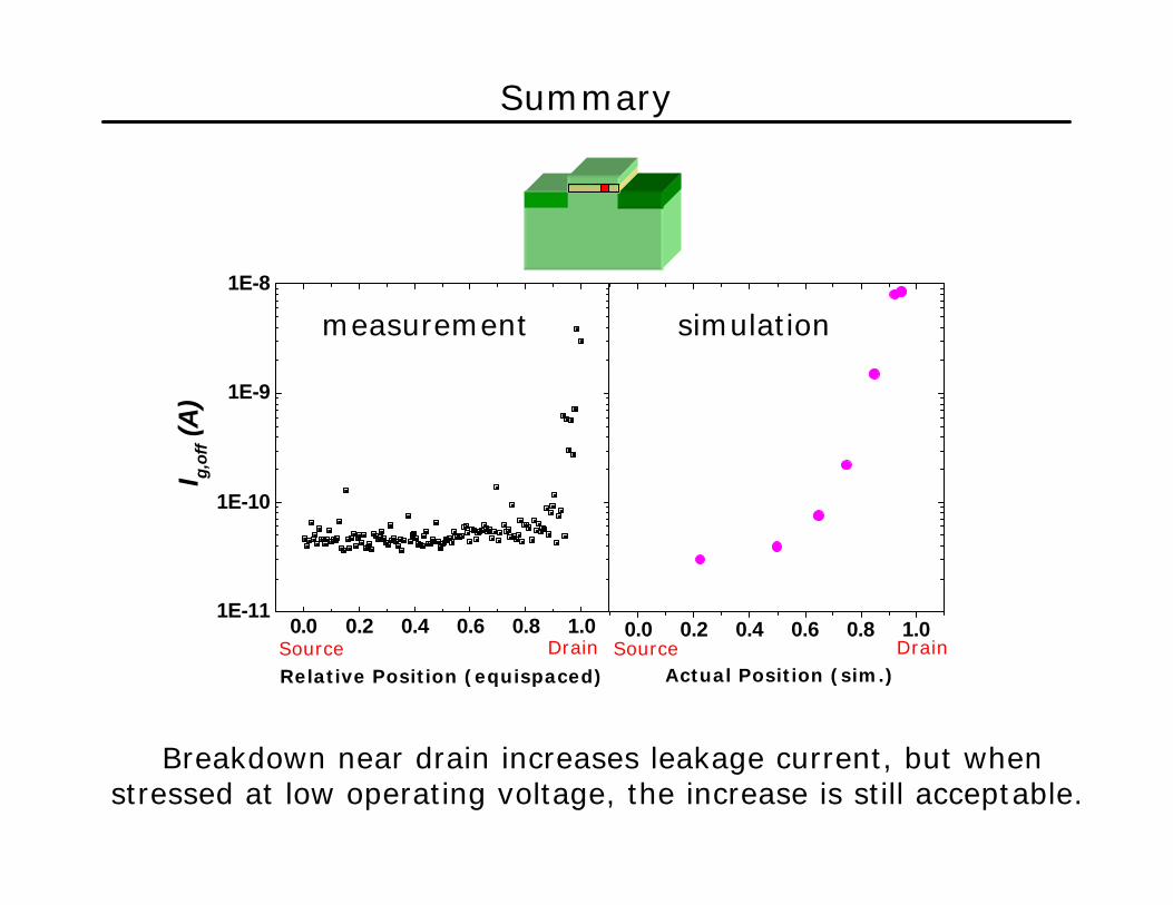
measurement simulation
Breakdown near drain increases leakage current, but whenstressed at low operating voltage, the increase is still acceptable.
0.0 0.2 0.4 0.6 0.8 1.01E-11
1E-10
1E-9
1E-8
DrainSourceDrainSource
I g,of
f (A
)
Relative Position (equispaced)
0.0 0.2 0.4 0.6 0.8 1.0
Actual Position (sim.)
Summary
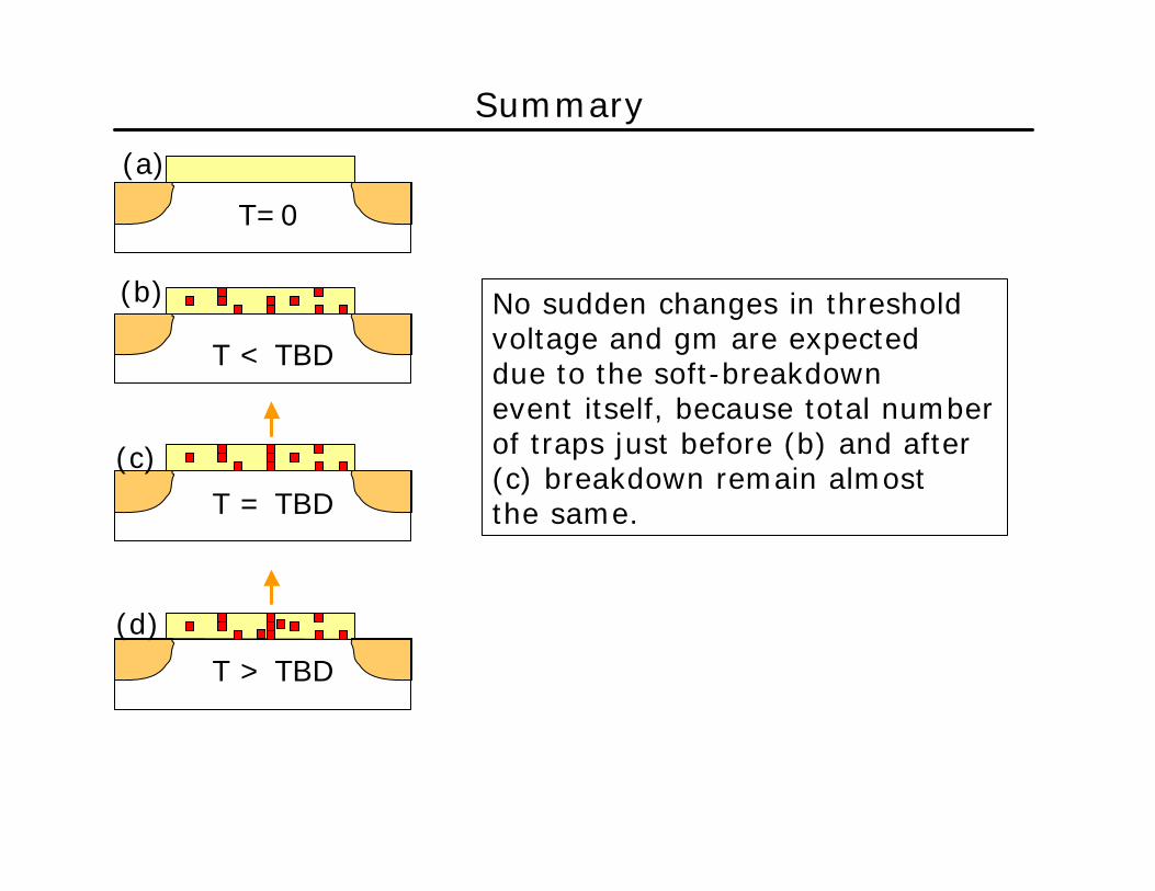
T=0
T < TBD
T = TBD
T > TBD
No sudden changes in threshold voltage and gm are expected due to the soft-breakdown event itself, because total numberof traps just before (b) and after (c) breakdown remain almost the same.
(a)
(b)
(c)
(d)
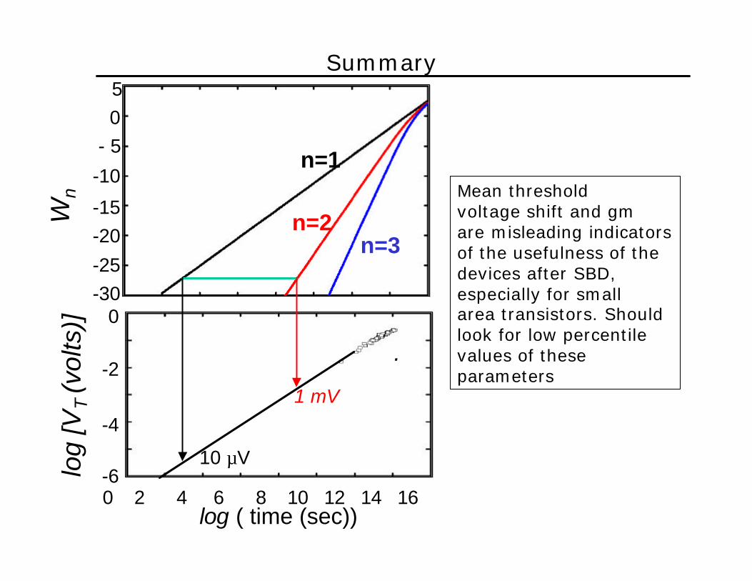
SummaryW
n
n=1
n=2n=3
50
-10
-15-20
-25-30
log ( time (sec))
- 5
log
[VT
(vol
ts)]
0 2 4 6 8 10 12 14 16-6
-4
-2
0
1 mV
10 µV
.
Mean threshold voltage shift and gm are misleading indicatorsof the usefulness of the devices after SBD, especially for smallarea transistors. Should look for low percentile values of these parameters
Summary
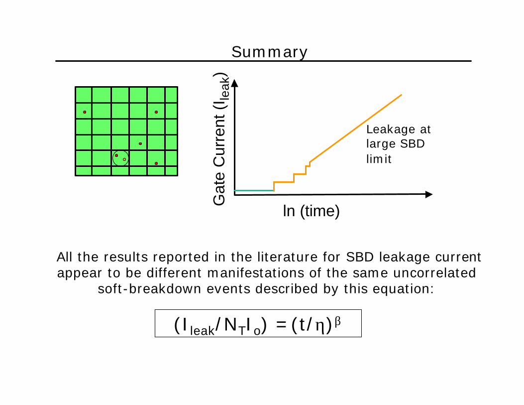
(Ileak/NTIo) =(t/η)β
ln (time)G
ate
Cur
rent
(I le
ak)
Leakage at large SBDlimit
All the results reported in the literature for SBD leakage currentappear to be different manifestations of the same uncorrelated
soft-breakdown events described by this equation:
Summary
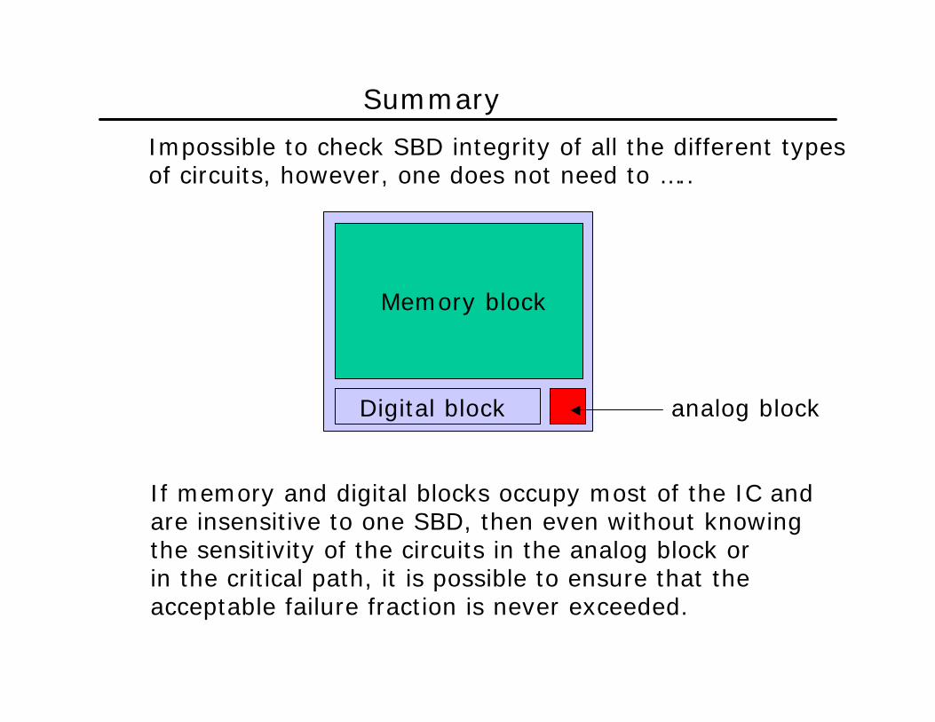
Memory block
Digital block analog block
If memory and digital blocks occupy most of the IC andare insensitive to one SBD, then even without knowing the sensitivity of the circuits in the analog block orin the critical path, it is possible to ensure that the acceptable failure fraction is never exceeded.
Impossible to check SBD integrity of all the different typesof circuits, however, one does not need to …..
Conclusions
q Study of soft-breakdown was curiosity-driven,but it may end up saving Moore’s law!
q Soft breakdown does not perturb transistor functionsignificantly and the fraction of soft-broken transistors in a given IC can be increased by reducing the operating voltage.
q If a transistor can sustain even one soft breakdown, the lifetime of the IC increases geometrically. Therefore, transistor scaling helps reliability!
q Soft breakdown currents are plotted in many different forms -the underlying physical phenomenon appears to be identical.
q Excess reliability can be traded for higher circuit speed. Oxide reliability, in the traditional sense, may no longer be a reliability concern.
q However, leakage limit (Power/EM) or threshold voltage limits (HCI/NBTI) must still be considered carefully.