Embed Size (px)
Citation preview

2

Contents
1 Introduction 71.1 Motivation and Design Goals . . . . . . . . . . . . . . . . . . . . . . . . . . . 71.2 Hardware Overview . . . . . . . . . . . . . . . . . . . . . . . . . . . . . . . . 8
1.2.1 Communication . . . . . . . . . . . . . . . . . . . . . . . . . . . . . . . 81.2.2 I/O Capabilities . . . . . . . . . . . . . . . . . . . . . . . . . . . . . . 81.2.3 Motor Drivers . . . . . . . . . . . . . . . . . . . . . . . . . . . . . . . . 9
2 User Guide 112.1 Getting Started . . . . . . . . . . . . . . . . . . . . . . . . . . . . . . . . . . . 112.2 Built-in Diagnostics and Configuration . . . . . . . . . . . . . . . . . . . . . . 11
2.2.1 OrcPad Calibration . . . . . . . . . . . . . . . . . . . . . . . . . . . . 122.2.2 OrcBoard Diagnostics and Configuration . . . . . . . . . . . . . . . . . 12
2.3 Connecting to the OrcBoard . . . . . . . . . . . . . . . . . . . . . . . . . . . . 122.4 Detailed Feature Descriptions . . . . . . . . . . . . . . . . . . . . . . . . . . . 13
2.4.1 Analog In . . . . . . . . . . . . . . . . . . . . . . . . . . . . . . . . . . 132.4.2 Analog Out . . . . . . . . . . . . . . . . . . . . . . . . . . . . . . . . . 142.4.3 Digital In . . . . . . . . . . . . . . . . . . . . . . . . . . . . . . . . . . 152.4.4 Digital Out . . . . . . . . . . . . . . . . . . . . . . . . . . . . . . . . . 152.4.5 Gyroscope Integrator . . . . . . . . . . . . . . . . . . . . . . . . . . . . 162.4.6 Motor Control . . . . . . . . . . . . . . . . . . . . . . . . . . . . . . . 172.4.7 PWM Generator . . . . . . . . . . . . . . . . . . . . . . . . . . . . . . 172.4.8 Servo Control . . . . . . . . . . . . . . . . . . . . . . . . . . . . . . . . 172.4.9 Sonar . . . . . . . . . . . . . . . . . . . . . . . . . . . . . . . . . . . . 182.4.10 Quadrature/Monophase Decoders . . . . . . . . . . . . . . . . . . . . 19
3 Power 213.1 Input Power . . . . . . . . . . . . . . . . . . . . . . . . . . . . . . . . . . . . . 213.2 Peripheral Power . . . . . . . . . . . . . . . . . . . . . . . . . . . . . . . . . . 223.3 Alternative Operating Voltages . . . . . . . . . . . . . . . . . . . . . . . . . . 22
4 Packet Communication 254.1 Packets . . . . . . . . . . . . . . . . . . . . . . . . . . . . . . . . . . . . . . . 25
4.1.1 Checksum Algorithm . . . . . . . . . . . . . . . . . . . . . . . . . . . . 264.1.2 Event Character Support . . . . . . . . . . . . . . . . . . . . . . . . . 26
4.2 Transaction Management . . . . . . . . . . . . . . . . . . . . . . . . . . . . . 264.2.1 Timeouts . . . . . . . . . . . . . . . . . . . . . . . . . . . . . . . . . . 264.2.2 Buffer Management . . . . . . . . . . . . . . . . . . . . . . . . . . . . 274.2.3 Asynchronous Events . . . . . . . . . . . . . . . . . . . . . . . . . . . 27
3

4 CONTENTS
5 Request API 295.1 Pin Modes . . . . . . . . . . . . . . . . . . . . . . . . . . . . . . . . . . . . . . 295.2 Simple Acknowledgments . . . . . . . . . . . . . . . . . . . . . . . . . . . . . 305.3 Master Requests . . . . . . . . . . . . . . . . . . . . . . . . . . . . . . . . . . 30
5.3.1 State Request . . . . . . . . . . . . . . . . . . . . . . . . . . . . . . . . 305.3.2 Analog Filter Set . . . . . . . . . . . . . . . . . . . . . . . . . . . . . . 325.3.3 Configure Clock . . . . . . . . . . . . . . . . . . . . . . . . . . . . . . 325.3.4 Configure Pin . . . . . . . . . . . . . . . . . . . . . . . . . . . . . . . . 325.3.5 Digital Out Set . . . . . . . . . . . . . . . . . . . . . . . . . . . . . . . 325.3.6 I2C Read . . . . . . . . . . . . . . . . . . . . . . . . . . . . . . . . . . 335.3.7 I2C Write . . . . . . . . . . . . . . . . . . . . . . . . . . . . . . . . . . 335.3.8 Servo Set . . . . . . . . . . . . . . . . . . . . . . . . . . . . . . . . . . 335.3.9 Sonar Initiate . . . . . . . . . . . . . . . . . . . . . . . . . . . . . . . . 33
5.4 Slave Requests . . . . . . . . . . . . . . . . . . . . . . . . . . . . . . . . . . . 345.4.1 State Request . . . . . . . . . . . . . . . . . . . . . . . . . . . . . . . . 345.4.2 All Stop . . . . . . . . . . . . . . . . . . . . . . . . . . . . . . . . . . . 355.4.3 Analog Filter Set . . . . . . . . . . . . . . . . . . . . . . . . . . . . . . 365.4.4 Configure Pin . . . . . . . . . . . . . . . . . . . . . . . . . . . . . . . . 365.4.5 Digital Out Set . . . . . . . . . . . . . . . . . . . . . . . . . . . . . . . 365.4.6 Motor Set . . . . . . . . . . . . . . . . . . . . . . . . . . . . . . . . . . 365.4.7 Motor Slew Set . . . . . . . . . . . . . . . . . . . . . . . . . . . . . . . 36
5.5 Pad Requests . . . . . . . . . . . . . . . . . . . . . . . . . . . . . . . . . . . . 365.5.1 State Request . . . . . . . . . . . . . . . . . . . . . . . . . . . . . . . . 375.5.2 Clear Display . . . . . . . . . . . . . . . . . . . . . . . . . . . . . . . . 385.5.3 Console Goto Cursor . . . . . . . . . . . . . . . . . . . . . . . . . . . . 385.5.4 Console Home Cursor . . . . . . . . . . . . . . . . . . . . . . . . . . . 385.5.5 Console Set Size . . . . . . . . . . . . . . . . . . . . . . . . . . . . . . 385.5.6 Console Write . . . . . . . . . . . . . . . . . . . . . . . . . . . . . . . . 395.5.7 Draw Mode Set . . . . . . . . . . . . . . . . . . . . . . . . . . . . . . . 395.5.8 Draw Lines . . . . . . . . . . . . . . . . . . . . . . . . . . . . . . . . . 395.5.9 Draw text . . . . . . . . . . . . . . . . . . . . . . . . . . . . . . . . . . 395.5.10 Draw top text . . . . . . . . . . . . . . . . . . . . . . . . . . . . . . . . 405.5.11 Draw Pixels . . . . . . . . . . . . . . . . . . . . . . . . . . . . . . . . . 405.5.12 Fill Display . . . . . . . . . . . . . . . . . . . . . . . . . . . . . . . . . 405.5.13 Raw read . . . . . . . . . . . . . . . . . . . . . . . . . . . . . . . . . . 405.5.14 Raw write . . . . . . . . . . . . . . . . . . . . . . . . . . . . . . . . . . 41
A Soldering and PCB Assembly 43A.1 Chemistry and Metallurgy of Soldering . . . . . . . . . . . . . . . . . . . . . . 43A.2 Soldering Tools . . . . . . . . . . . . . . . . . . . . . . . . . . . . . . . . . . . 44A.3 Assembly Strategy . . . . . . . . . . . . . . . . . . . . . . . . . . . . . . . . . 45A.4 Making Cables . . . . . . . . . . . . . . . . . . . . . . . . . . . . . . . . . . . 45A.5 Assembling through-hole devices . . . . . . . . . . . . . . . . . . . . . . . . . 47A.6 Assembling SMT devices . . . . . . . . . . . . . . . . . . . . . . . . . . . . . . 47
B LCD Memory Map 51
C The OrcPad as a Prototyping Board 53
D Orcd, The Orc Communications Manager 55

CONTENTS 5
E Firmware Overview 57E.1 Pin Reconfiguration . . . . . . . . . . . . . . . . . . . . . . . . . . . . . . . . 57E.2 Interrupts and Performance . . . . . . . . . . . . . . . . . . . . . . . . . . . . 57E.3 Master . . . . . . . . . . . . . . . . . . . . . . . . . . . . . . . . . . . . . . . . 58E.4 Slave . . . . . . . . . . . . . . . . . . . . . . . . . . . . . . . . . . . . . . . . . 59E.5 Pad . . . . . . . . . . . . . . . . . . . . . . . . . . . . . . . . . . . . . . . . . 59
F Schematics 61F.1 Design Notes . . . . . . . . . . . . . . . . . . . . . . . . . . . . . . . . . . . . 61
F.1.1 Conventions . . . . . . . . . . . . . . . . . . . . . . . . . . . . . . . . . 61F.1.2 Power Supply . . . . . . . . . . . . . . . . . . . . . . . . . . . . . . . . 61F.1.3 Motor Drivers . . . . . . . . . . . . . . . . . . . . . . . . . . . . . . . . 61F.1.4 Cut Header . . . . . . . . . . . . . . . . . . . . . . . . . . . . . . . . . 61F.1.5 Communications . . . . . . . . . . . . . . . . . . . . . . . . . . . . . . 62
F.2 OrcBoard Schematics . . . . . . . . . . . . . . . . . . . . . . . . . . . . . . . . 62F.3 OrcPad Schematics . . . . . . . . . . . . . . . . . . . . . . . . . . . . . . . . . 69

6 CONTENTS

Chapter 1
Introduction
1.1 Motivation and Design Goals
The Orc hardware, now in its 4th revision, was designed to support the MASLab RoboticsCompetition, held yearly at MIT. It is intended to simplify the task of building robots,balancing cost and flexibility.
Figure 1.1: MASLab 2004. The OrcBoard was design for use in MIT’s Mobile AutonomousSystems Laboratory (MASLab) robotics competition.
The OrcBoard was inspired by the HandyBoard, produced for MIT’s 6.270 roboticscompetition. The HandyBoard was remarkable in its day, but it is now a 20 year-old design,and does not make good use of the high-density devices available today.
A fundamental design decision behind the OrcBoard is to separate the computationalmachinery (“compute”) from the robotics interface. The OrcBoard is the robotics interface–allowing the compute to read and control sensors and actuators. Factoring the design inthis way allows robot implementors to pick a compute engine that is appropriate for them.The compute can be any device with a serial or USB port, ranging from a lowly PIC to alaptop.
The OrcBoard was also designed for maximum hackability. The board is constructedusing hobbyist-accessible technologies, using only simple SMT devices and socketed DIPswhenever possible. In addition, the firmware on the OrcBoard can be readily modified tochange the functionality. For example, it is possible to support over a dozen servos bysacrificing other capabilities.
7
8 CHAPTER 1. INTRODUCTION
The OrcBoard has a companion, the OrcPad, which provides a rich user interface, includ-ing a 128x64 pixel LCD panel, a two-axis analog joystick, and three push buttons (includingan “emergency stop” button). The OrcPad is extremely useful for robots whose computelacks a display, as well as for dumping diagnostic information. The OrcPad is attached tothe OrcBoard via a tether that can extend up to three meters. In addition, the OrcBoardcontains firmware for performing basic diagnostic functions on the OrcBoard’s ports, as wellas experimenting with motors and sensors. For example, without any compute engine, it ispossible to drive a robot around using built-in firmware.
1.2 Hardware Overview
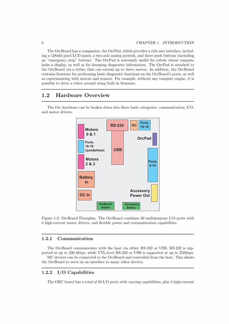
The Orc hardware can be broken down into three basic categories: communication, I/O,and motor drivers.
USB
RS-232Ports
16-19
OrcPad
Ports
0-15
Accessory
Power Out
Accessory
Switch
OrcBoard
Switch
DC In
Battery
In
Motors
0 & 1
Motors
2 & 3
Ports
16-19
(quadphase)
I2C
Figure 1.2: OrcBoard Floorplan. The OrcBoard combines 20 multipurpose I/O ports with4 high-current motor drivers, and flexible power and communication capabilities.
1.2.1 Communication
The OrcBoard communicates with the host via either RS-232 or USB. RS-232 is sup-ported at up to 230.4kbps, while TTL-level RS-232 or USB is supported at up to 250kbps.
I2C devices can be connected to the OrcBoard and controlled from the host. This allowsthe OrcBoard to serve as an interface to many other devices.
1.2.2 I/O Capabilities
The ORC board has a total of 20 I/O ports with varying capabilities, plus 4 high-current
1.2. HARDWARE OVERVIEW 9
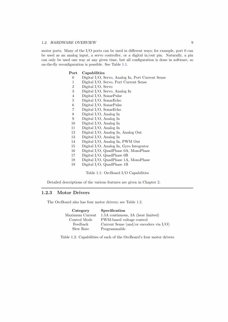
motor ports. Many of the I/O ports can be used in different ways; for example, port 0 canbe used as an analog input, a servo controller, or a digital in/out pin. Naturally, a pincan only be used one way at any given time, but all configuration is done in software, soon-the-fly reconfiguration is possible. See Table 1.1.
Port Capabilities0 Digital I/O, Servo, Analog In, Port Current Sense1 Digital I/O, Servo, Port Current Sense2 Digital I/O, Servo3 Digital I/O, Servo, Analog In4 Digital I/O, SonarPulse5 Digital I/O, SonarEcho6 Digital I/O, SonarPulse7 Digital I/O, SonarEcho8 Digital I/O, Analog In9 Digital I/O, Analog In10 Digital I/O, Analog In11 Digital I/O, Analog In12 Digital I/O, Analog In, Analog Out13 Digital I/O, Analog In14 Digital I/O, Analog In, PWM Out15 Digital I/O, Analog In, Gyro Integrator16 Digital I/O, QuadPhase 0A, MonoPhase17 Digital I/O, QuadPhase 0B18 Digital I/O, QuadPhase 1A, MonoPhase19 Digital I/O, QuadPhase 1B
Table 1.1: OrcBoard I/O Capabilities
Detailed descriptions of the various features are given in Chapter 2.
1.2.3 Motor Drivers
The OrcBoard also has four motor drivers; see Table 1.2.
Category SpecificationMaximum Current 1.5A continuous, 3A (heat limited)
Control Mode PWM-based voltage controlFeedback Current Sense (and/or encoders via I/O)Slew Rate Programmable
Table 1.2: Capabilities of each of the OrcBoard’s four motor drivers

10 CHAPTER 1. INTRODUCTION
Chapter 2
User Guide
The OrcBoard and OrcPad have extensive functionality built into them. The boards actuallycontain a total of three microcontrollers. These microcontrollers, known as ProgrammableSystems on a Chip (PSoCs) are manufactured by Cypress Microsystems. They run at24MHz, executing a typical instruction in around 6 cycles; they also have 2KB of RAM and32KB of FLASH.
Rather than providing crude I/O capabilities, the microcontrollers are put to work,providing higher-level functionality and simplifying the task of the user.
A major concern in robotics are real-time constraints. Some events require very precisetiming, and if the required timing is not achieved, some type of failure can occur. TheOrcBoard is designed to handle most of a robot’s real-time activities; this is where the“hidden” CPU power of the OrcBoard comes in handy. The host controller can worryabout high-level control issues, leaving the timing-sensitive tasks to the OrcBoard.
2.1 Getting Started
Before using the OrcBoard/OrcPad:
• Inspect the board for missing or bridged solder joints.
• Review the power requirements section.
• Ensure that the battery is fused.
• Disconnect all motors and sensors.
When the OrcBoard starts up, the OrcPad will display a splash screen, and should displaythe text “Self-tests passed”. If self-tests fail, or no message regarding self-tests appears,then the OrcBoard is malfunctioning. Do not proceed until the problem is diagnosed andcorrected.
If the tests pass, proceed to configure and calibrate the OrcBoard and OrcPad.
2.2 Built-in Diagnostics and Configuration
The OrcBoard and OrcPad persistently maintain configuration information which gov-erns their operation. This data will be lost when firmware is upgraded, but it will survivepower-cycling. In addition, the firmware contains various utilities which can be useful whenworking on a robot.
11
12 CHAPTER 2. USER GUIDE
2.2.1 OrcPad Calibration
The OrcPad calibration should be performed first, in order to calibrate the joystick;otherwise, navigating other menus may prove difficult.
To enter the OrcPad calibration, hold down the menu button for four seconds. After onesecond, the OrcBoard configuration screen will pop up; this will be described in the nextsection. Ignore this screen and continue to hold down the menu button until four secondshave passed.
Follow the on-screen prompts to calibrate the joystick. Make sure that the joysticktravels around its full range of motion, and be sure to leave the joystick centered beforetapping “menu” and proceeding to the next configuration screen.
The second step of OrcPad calibration is to fine-tune the battery voltage sensor. Use amultimeter to measure the voltage currently being applied to the OrcBoard, be it from abattery or wall adapter. Use the joystick to adjust the displayed voltage until it matchesthe reading on the multimeter.
Confirm that you are done calibrating by tapping menu again. The changes will bewritten to the OrcPad’s FLASH memory.
2.2.2 OrcBoard Diagnostics and Configuration
Enter the OrcBoard configuration screen by holding down the OrcPad’s “menu” buttonfor one second. A menu will be displayed with various options for examining the state of theOrcBoard. Most of these options are self-explanatory, however two deserve special mention.
Drive Mode
Most differentially-driven robots (those with two motors, each connected to a wheel onopposite sides of the robot) can be driven from the OrcBoard’s firmware, without writingany code.
Drive Mode assumes that the drive motors are connected to ports 0 and 2. Movementsof the joystick are translated into PWM control signals to the joystick.
Configuration
Communication parameters, such as baud rate, can be configured in the OrcBoard firmware.These changes are written to FLASH, and so are remembered every time the OrcBoard startsup.
2.3 Connecting to the OrcBoard
The OrcBoard can be accessed in three ways.
• The DB-9 connector provides an RS-232 interface with +/- 10V signaling.
• TTL-level RS-232 signals can be accessed from header. This is intended for smallcompute platforms (PICs, Basic STAMPs), avoiding the need for them to use a chargepump.
• The OrcBoard can be outfitted with a USBMOD3 device, which will provide a USBinterface to the board.
2.4. DETAILED FEATURE DESCRIPTIONS 13
Despite the extremely-high bandwidth available over USB, the OrcBoard in generalperforms a little worse over USB than a serial connection. There are two causes: the first(and most important) cause is the very high latency of the USB bus, which artificially addsdelays to packet reception. The second reason is that the OrcBoard only communicateswith the USB module at 250kbps, limiting the maximum achievable bandwidth to a smallfraction of USB’s theoretical capacity. While OrcBoard/Host communication is slower thanit could be, it is plenty fast for virtually any robotics application.
If the OrcBoard is being used via USB, placing it on the same USB bus as a high-bandwidth device such as a camera should be avoided.
Once a physical connection is made to the OrcBoard, most users will use prewrittenlibraries to actually issue requests and receive data. These libraries vary from platform toplatform and are consequently documented separately. However, these libraries all imple-ment the protocols described in this document in Chapters 4 and 5.
2.4 Detailed Feature Descriptions
When writing software for the OrcBoard, the first step is to decide which features areneeded, and to decide which combination of pin configurations will be best.
The host controller should initialize each pin before it begins controlling the robot. Thismust be done every time the OrcBoard is reset; the OrcBoard always starts-up in a “safe”configuration which will probably not match your robot’s requirements.
Each pin can be used in a variety of modes. The set of modes available on each pinvaries; see Table 1.1 for a list of capabilities. The modes are described in more detail below.
Warning! It is possible to damage the OrcBoard or sensors attached to it by in-correctly configuring ports or plugging in sensors incorrectly. The most dangerous modesare those that cause a pin to be an “output”. If an “output” pin (e.g., Analog Out, DigitalOut, Servo, Sonar Pulse, PWM Generator) is connected to another device which is also an“output” (e.g., analog range finder, digital switches), damage to either the device and/orthe OrcBoard can occur!
For example, connecting an analog range finder to a port configured as a digital outcauses contention: two devices both trying to make the same signal have the same voltage.Just like shorting power and ground, this can cause a lot of current to flow and can damagethe device.
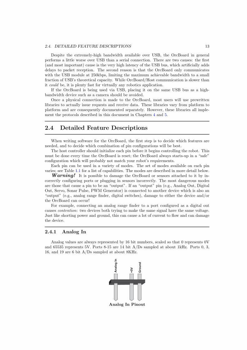
2.4.1 Analog In
Analog values are always represented by 16 bit numbers, scaled so that 0 represents 0Vand 65535 represents 5V. Ports 8-15 are 14 bit A/Ds sampled at about 1kHz. Ports 0, 3,16, and 19 are 6 bit A/Ds sampled at about 8KHz.
Gro
un
d
+5V
An
alo
g In
Analog In Pinout
14 CHAPTER 2. USER GUIDE
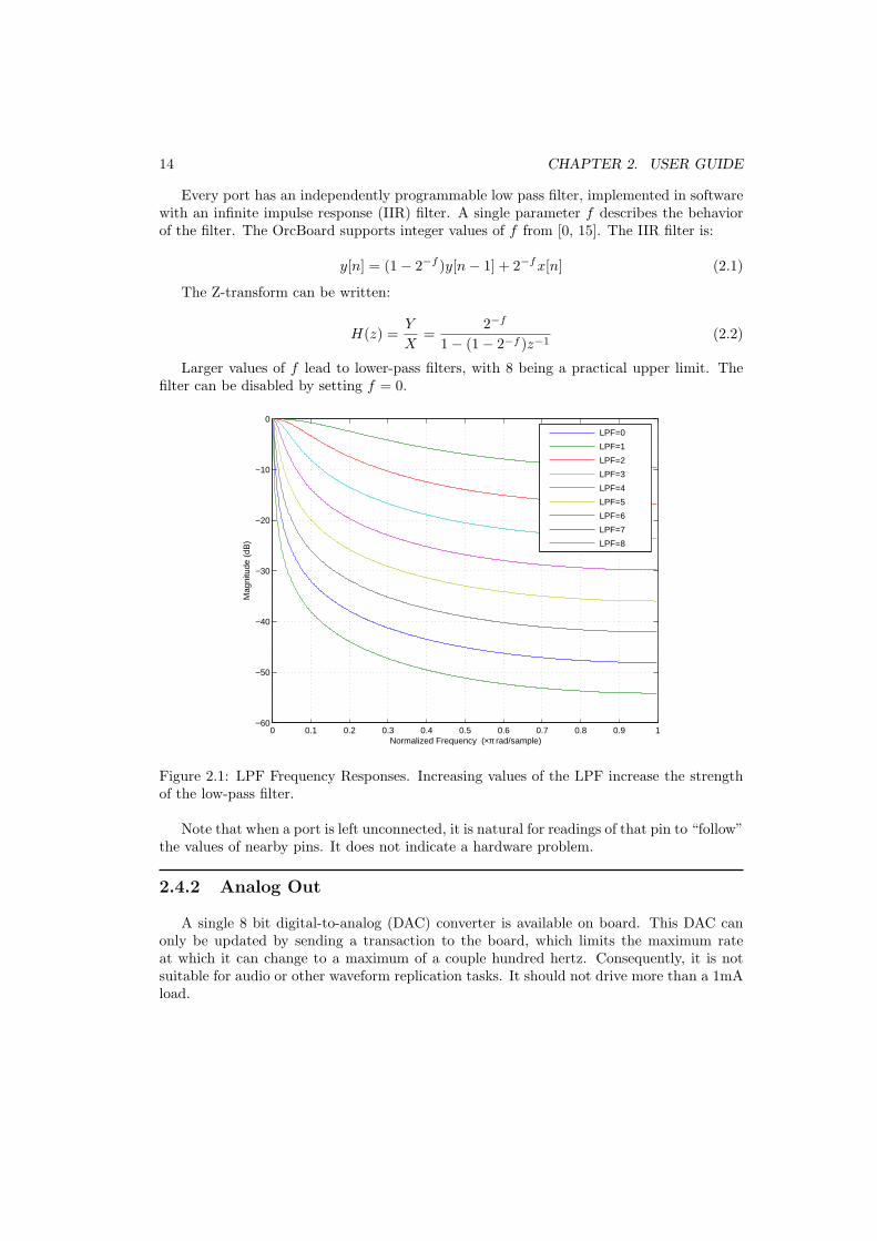
Every port has an independently programmable low pass filter, implemented in softwarewith an infinite impulse response (IIR) filter. A single parameter f describes the behaviorof the filter. The OrcBoard supports integer values of f from [0, 15]. The IIR filter is:
y[n] = (1− 2−f )y[n− 1] + 2−fx[n] (2.1)
The Z-transform can be written:
H(z) =Y
X=
2−f
1− (1− 2−f )z−1(2.2)
Larger values of f lead to lower-pass filters, with 8 being a practical upper limit. Thefilter can be disabled by setting f = 0.
0 0.1 0.2 0.3 0.4 0.5 0.6 0.7 0.8 0.9 1−60
−50
−40
−30
−20
−10
0
Normalized Frequency (×π rad/sample)
Mag
nitu
de (
dB)
LPF=0
LPF=1
LPF=2
LPF=3
LPF=4
LPF=5
LPF=6
LPF=7
LPF=8
Figure 2.1: LPF Frequency Responses. Increasing values of the LPF increase the strengthof the low-pass filter.
Note that when a port is left unconnected, it is natural for readings of that pin to “follow”the values of nearby pins. It does not indicate a hardware problem.
2.4.2 Analog Out
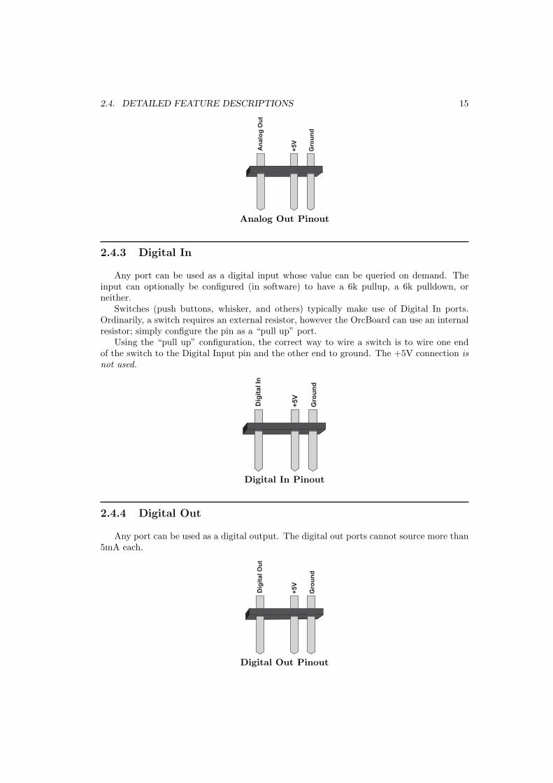
A single 8 bit digital-to-analog (DAC) converter is available on board. This DAC canonly be updated by sending a transaction to the board, which limits the maximum rateat which it can change to a maximum of a couple hundred hertz. Consequently, it is notsuitable for audio or other waveform replication tasks. It should not drive more than a 1mAload.
2.4. DETAILED FEATURE DESCRIPTIONS 15
Gro
un
d
+5V
An
alo
g O
ut
Analog Out Pinout
2.4.3 Digital In
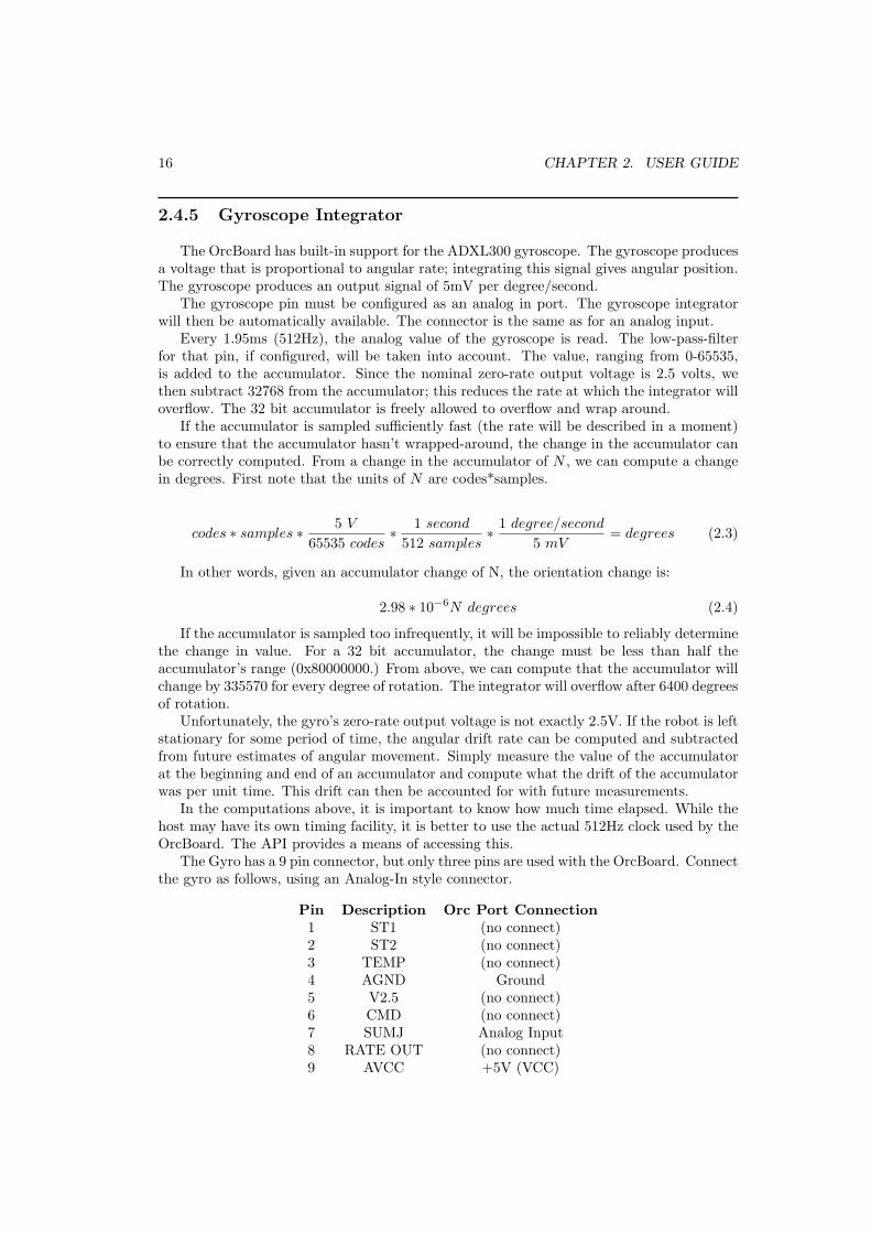
Any port can be used as a digital input whose value can be queried on demand. Theinput can optionally be configured (in software) to have a 6k pullup, a 6k pulldown, orneither.
Switches (push buttons, whisker, and others) typically make use of Digital In ports.Ordinarily, a switch requires an external resistor, however the OrcBoard can use an internalresistor; simply configure the pin as a “pull up” port.
Using the “pull up” configuration, the correct way to wire a switch is to wire one endof the switch to the Digital Input pin and the other end to ground. The +5V connection isnot used.
Gro
un
d
+5
V
Dig
ita
l In
Digital In Pinout
2.4.4 Digital Out
Any port can be used as a digital output. The digital out ports cannot source more than5mA each.
Gro
un
d
+5
V
Dig
ita
l O
ut
Digital Out Pinout
16 CHAPTER 2. USER GUIDE
2.4.5 Gyroscope Integrator
The OrcBoard has built-in support for the ADXL300 gyroscope. The gyroscope producesa voltage that is proportional to angular rate; integrating this signal gives angular position.The gyroscope produces an output signal of 5mV per degree/second.
The gyroscope pin must be configured as an analog in port. The gyroscope integratorwill then be automatically available. The connector is the same as for an analog input.
Every 1.95ms (512Hz), the analog value of the gyroscope is read. The low-pass-filterfor that pin, if configured, will be taken into account. The value, ranging from 0-65535,is added to the accumulator. Since the nominal zero-rate output voltage is 2.5 volts, wethen subtract 32768 from the accumulator; this reduces the rate at which the integrator willoverflow. The 32 bit accumulator is freely allowed to overflow and wrap around.
If the accumulator is sampled sufficiently fast (the rate will be described in a moment)to ensure that the accumulator hasn’t wrapped-around, the change in the accumulator canbe correctly computed. From a change in the accumulator of N , we can compute a changein degrees. First note that the units of N are codes*samples.
codes ∗ samples ∗ 5 V
65535 codes∗ 1 second
512 samples∗ 1 degree/second
5 mV= degrees (2.3)
In other words, given an accumulator change of N, the orientation change is:
2.98 ∗ 10−6N degrees (2.4)
If the accumulator is sampled too infrequently, it will be impossible to reliably determinethe change in value. For a 32 bit accumulator, the change must be less than half theaccumulator’s range (0x80000000.) From above, we can compute that the accumulator willchange by 335570 for every degree of rotation. The integrator will overflow after 6400 degreesof rotation.
Unfortunately, the gyro’s zero-rate output voltage is not exactly 2.5V. If the robot is leftstationary for some period of time, the angular drift rate can be computed and subtractedfrom future estimates of angular movement. Simply measure the value of the accumulatorat the beginning and end of an accumulator and compute what the drift of the accumulatorwas per unit time. This drift can then be accounted for with future measurements.
In the computations above, it is important to know how much time elapsed. While thehost may have its own timing facility, it is better to use the actual 512Hz clock used by theOrcBoard. The API provides a means of accessing this.
The Gyro has a 9 pin connector, but only three pins are used with the OrcBoard. Connectthe gyro as follows, using an Analog-In style connector.
Pin Description Orc Port Connection1 ST1 (no connect)2 ST2 (no connect)3 TEMP (no connect)4 AGND Ground5 V2.5 (no connect)6 CMD (no connect)7 SUMJ Analog Input8 RATE OUT (no connect)9 AVCC +5V (VCC)
2.4. DETAILED FEATURE DESCRIPTIONS 17
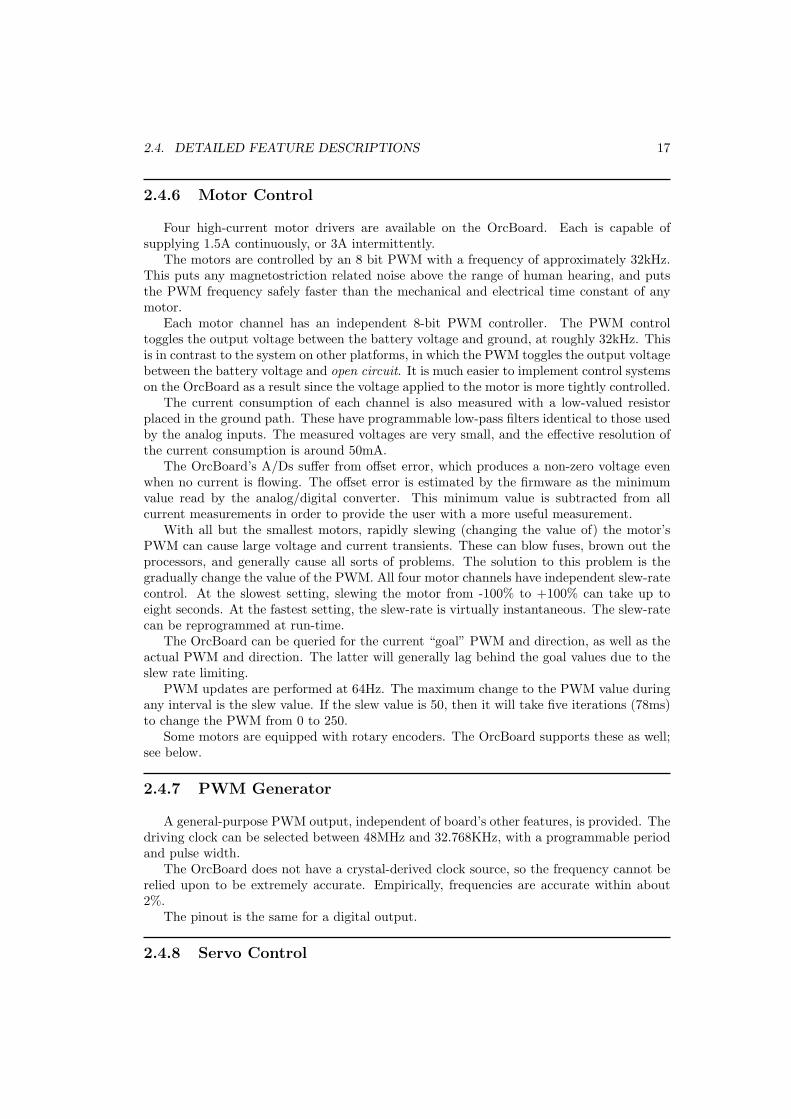
2.4.6 Motor Control
Four high-current motor drivers are available on the OrcBoard. Each is capable ofsupplying 1.5A continuously, or 3A intermittently.
The motors are controlled by an 8 bit PWM with a frequency of approximately 32kHz.This puts any magnetostriction related noise above the range of human hearing, and putsthe PWM frequency safely faster than the mechanical and electrical time constant of anymotor.
Each motor channel has an independent 8-bit PWM controller. The PWM controltoggles the output voltage between the battery voltage and ground, at roughly 32kHz. Thisis in contrast to the system on other platforms, in which the PWM toggles the output voltagebetween the battery voltage and open circuit. It is much easier to implement control systemson the OrcBoard as a result since the voltage applied to the motor is more tightly controlled.
The current consumption of each channel is also measured with a low-valued resistorplaced in the ground path. These have programmable low-pass filters identical to those usedby the analog inputs. The measured voltages are very small, and the effective resolution ofthe current consumption is around 50mA.
The OrcBoard’s A/Ds suffer from offset error, which produces a non-zero voltage evenwhen no current is flowing. The offset error is estimated by the firmware as the minimumvalue read by the analog/digital converter. This minimum value is subtracted from allcurrent measurements in order to provide the user with a more useful measurement.
With all but the smallest motors, rapidly slewing (changing the value of) the motor’sPWM can cause large voltage and current transients. These can blow fuses, brown out theprocessors, and generally cause all sorts of problems. The solution to this problem is thegradually change the value of the PWM. All four motor channels have independent slew-ratecontrol. At the slowest setting, slewing the motor from -100% to +100% can take up toeight seconds. At the fastest setting, the slew-rate is virtually instantaneous. The slew-ratecan be reprogrammed at run-time.
The OrcBoard can be queried for the current “goal” PWM and direction, as well as theactual PWM and direction. The latter will generally lag behind the goal values due to theslew rate limiting.
PWM updates are performed at 64Hz. The maximum change to the PWM value duringany interval is the slew value. If the slew value is 50, then it will take five iterations (78ms)to change the PWM from 0 to 250.
Some motors are equipped with rotary encoders. The OrcBoard supports these as well;see below.
2.4.7 PWM Generator
A general-purpose PWM output, independent of board’s other features, is provided. Thedriving clock can be selected between 48MHz and 32.768KHz, with a programmable periodand pulse width.
The OrcBoard does not have a crystal-derived clock source, so the frequency cannot berelied upon to be extremely accurate. Empirically, frequencies are accurate within about2%.
The pinout is the same for a digital output.
2.4.8 Servo Control
18 CHAPTER 2. USER GUIDE
Up to four Futaba-style servos can be controlled on the OrcBoard. Servos are imple-mented with 16 bit PWM, clocked at 16MHz. A single PWM module is time-multiplexedbetween the four servo outputs. Consequently, the maximum duty cycle for any servo is25%.
Gro
un
d
+5
V
Se
rv
o O
ut
Servo Pinout
Ports 0 and 1 support a current-sense feature, designed to measure the current consump-tion of servos. Current consumption is directly proportional to torque, so the current-sensecan be used to detect how much resistance the servo is experiencing.
Servos draw current in pulses, so a hardware low-pass filter (an RC filter with a timeconstant of 33ms) is used to produce a more readily useful measurement.
The servo connectors are designed to be easily interfaced with the three-pin connectorsfound on most servos. However, both the servo’s connector and the OrcBoard connectorare female. Rather than replacing the servo’s connector, we suggest using a 3x1 section ofwire-wrap header, which can reliably serve as a coupler.
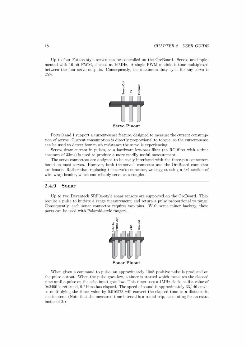
2.4.9 Sonar
Up to two Devantech SRF04-style sonar sensors are supported on the OrcBoard. Theyrequire a pulse to initiate a range measurement, and return a pulse proportional to range.Consequently, each sonar connector requires two pins. With some minor hackery, theseports can be used with Polaroid-style rangers.
Gro
un
d
+5
V
Pu
lse
Ou
t
Ec
ho
In
Sonar Pinout
When given a command to pulse, an approximately 10uS positive pulse is produced onthe pulse output. When the pulse goes low, a timer is started which measures the elapsedtime until a pulse on the echo input goes low. This timer uses a 1MHz clock, so if a value of0x2400 is returned, 9.216ms has elapsed. The speed of sound is approximately 33,146 cm/s,so multiplying the timer value by 0.016573 will convert the elapsed time to a distance incentimeters. (Note that the measured time interval is a round-trip, accounting for an extrafactor of 2.)
2.4. DETAILED FEATURE DESCRIPTIONS 19
Warning! Use great care when inserting a sonar connector. It must be plugged intoPorts 4/5 or Ports 6/7. Plugging it “off by one”, such as 3/4, or 5/6 can damage the device.Also ensure that the ports have been properly configured!
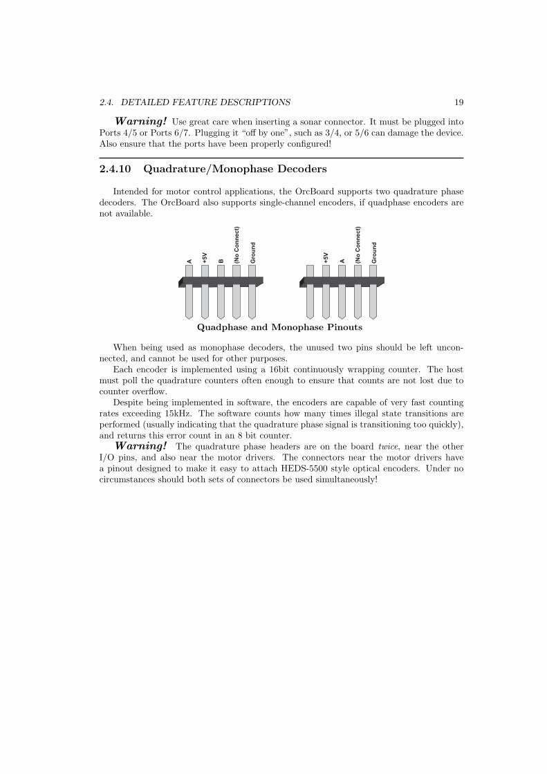
2.4.10 Quadrature/Monophase Decoders
Intended for motor control applications, the OrcBoard supports two quadrature phasedecoders. The OrcBoard also supports single-channel encoders, if quadphase encoders arenot available.
Gro
un
d
(No
Co
nn
ect)
+5V
BA Gro
un
d
(No
Co
nn
ect)
+5V
A
Quadphase and Monophase Pinouts
When being used as monophase decoders, the unused two pins should be left uncon-nected, and cannot be used for other purposes.
Each encoder is implemented using a 16bit continuously wrapping counter. The hostmust poll the quadrature counters often enough to ensure that counts are not lost due tocounter overflow.
Despite being implemented in software, the encoders are capable of very fast countingrates exceeding 15kHz. The software counts how many times illegal state transitions areperformed (usually indicating that the quadrature phase signal is transitioning too quickly),and returns this error count in an 8 bit counter.
Warning! The quadrature phase headers are on the board twice, near the otherI/O pins, and also near the motor drivers. The connectors near the motor drivers havea pinout designed to make it easy to attach HEDS-5500 style optical encoders. Under nocircumstances should both sets of connectors be used simultaneously!

20 CHAPTER 2. USER GUIDE
Chapter 3
Power
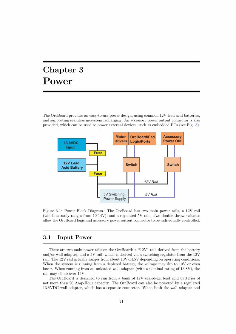
The OrcBoard provides an easy-to-use power design, using common 12V lead acid batteries,and supporting seamless in-system recharging. An accessory power output connector is alsoprovided, which can be used to power external devices, such as embedded PCs (see Fig. 3).
Fuse
Fuse
12V Rail
5V Rail
13.8VDC
Input
12V Lead
Acid Battery
5V Switching
Power Supply
Switch Switch
Accessory
Power Out Motor
DriversOrcBoard/Pad
Logic/Ports
Figure 3.1: Power Block Diagram. The OrcBoard has two main power rails, a 12V rail(which actually ranges from 10-14V), and a regulated 5V rail. Two double-throw switchesallow the OrcBoard logic and accessory power output connector to be individually controlled.
3.1 Input Power
There are two main power rails on the OrcBoard: a “12V” rail, derived from the batteryand/or wall adapter, and a 5V rail, which is derived via a switching regulator from the 12Vrail. The 12V rail actually ranges from about 10V-14.5V depending on operating conditions.When the system is running from a depleted battery, the voltage may dip to 10V or evenlower. When running from an unloaded wall adapter (with a nominal rating of 13.8V), therail may climb over 14V.
The OrcBoard is designed to run from a bank of 12V sealed-gel lead acid batteries ofnot more than 20 Amp-Hour capacity. The OrcBoard can also be powered by a regulated13.8VDC wall adapter, which has a separate connector. When both the wall adapter and
21
22 CHAPTER 3. POWER
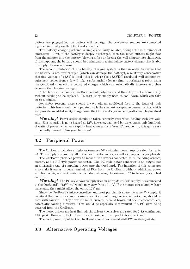
battery are plugged in, the battery will recharge; the two power sources are connectedtogether internally on the OrcBoard via a fuse.
This battery charging scheme is simple and fairly reliable, though it has a number oflimitations. First, if the battery is deeply discharged, then too much current might flowfrom the adapter into the battery, blowing a fuse or forcing the wall adapter into shutdown.If this happens, the battery should be recharged in a standalone battery charger that is ableto supply the needed current.
The second limitation of this battery charging system is that in order to ensure thatthe battery is not over-charged (which can damage the battery), a relatively conservativecharging voltage of 13.8V is used (this is where the 13.8VDC regulated wall adapter re-quirement comes from.) It will take a substantially longer time to recharge a robot usingthe OrcBoard than with a dedicated charger which can automatically increase and thendecrease the charging voltage.
Note that the fuses on the OrcBoard are all poly-fuses, and that they reset automaticallywithout needing to be replaced. To reset, they simply need to cool down, which can takeup to a minute.
For safety reasons, users should always add an additional fuse to the leads of theirbatteries. This fuse should be populated with the smallest acceptable current rating, whichwill provide an added safety margin over the OrcBoard’s permanently-attached, high-valuedfuses.
Warning! Power safety should be taken seriously even when dealing with low volt-ages. Electrocution is not a hazard at 12V, however, lead-acid batteries can supply hundredsof watts of power, which can rapidly heat wires and surfaces. Consequently, it is quite easyto be badly burned. Fuse your batteries!
3.2 Peripheral Power
The OrcBoard includes a high-performance 5V switching power supply rated for up to5A. This supply is shared by all of the board’s electronics, as well as many of its peripherals.
The OrcBoard provides power to most of the devices connected to it, including sensors,motors, and a PC-style power connector. The PC-style power connector is an output, notan alternative way of supplying power into the OrcBoard. The intention of this connectoris to make it easier to power embedded PCs from the OrcBoard without additional powersupplies. A high-current switch is included, allowing the external PC to be easily switchedon or off.
Warning! The PC-style power supply uses an unregulated 12V supply; it is connectedto the OrcBoard’s “12V” rail which may vary from 10-14V. If the motors cause large voltagetransients, they might affect the entire 12V rail.
Since the OrcBoard’s microcontrollers and most peripherals share the same 5V supply, itis critical that none draw an excessive amount current. Large servos, in particular, should beused with caution. If they draw too much current, it could brown out the microcontrollers,potentially causing a restart. This would be especially inconvenient if a PC were beingpowered from the OrcBoard.
The motor drivers are heat limited; the drivers themselves are rated for 2.8A continuous,5.6A peak. However, the OrcBoard is not designed to support this current load.
The total power input to the OrcBoard should not exceed 4A@12V in steady-state.
3.3 Alternative Operating Voltages
3.3. ALTERNATIVE OPERATING VOLTAGES 23
The OrcBoard can actually operate over a range of 8-24 VDC. Under 8V, the motordrivers will go into a safety shutdown. At voltages over 12V, the power delivered by themotor drivers grows very rapidly (power grows as V 2/R), so great care should be taken toensure that they do not overheat.
An alternative operating voltage can be achieved by building a battery pack out ofsmaller batteries. Three 6V batteries in series yields 18V, and two 12V batteries (againin series) yields 24V. These can be charged in-system as well, provided a wall adapter issuitably selected (it should be roughly 115% of the battery voltage.) However, these highervoltage systems can draw much more current, so it is probably wiser to give up on in-systemrecharging and use an external charger.
Using an alternative voltage will naturally affect the PC-style connector’s “12V” powerline. It would not be advisable to plug in a computer component if the 12V rail was actually24V.

24 CHAPTER 3. POWER
Chapter 4
Packet Communication
4.1 Packets
The OrcBoard/OrcPad is implemented using three separate microcontrollers. Packetsare routed between the chips, with one chip (the “master” on the OrcBoard) serving as ahub for all communication. Multiple packets can be in flight simultaneously.
The master serves as a router, with dedicated serial connections to the slave, the pad,and the host. Each connection is constantly monitored for incoming packets. When one isreceived, it is forwarded to the appropriate destination device. If the destination device isthe master, then the master processes the packet (it could be either a request or a responsefrom another device.)
Packets (Table 4.1) are variable-length and contain various bookkeeping information.
Offset Description0 Always the value 237 (0xED)1 The length of the packet2 Flags (routing information and transaction ID)3 First byte of data... (more data)
length− 1 Modified checksum byte
Table 4.1: Format of a packet
Each packet begins with a synchronization byte, which is always the value 0xED. Asynchronization byte makes it easier to identify the beginning of a packet, skipping overcorrupted data.
The second byte of every packet is the flags byte. The flags byte contains two fields: therouting field and the transaction ID. The high two bits are the routing flags. The lower sixbits are a user-definable transaction id. When the OrcBoard is replying to a request, thereply message will have the same transaction ID as the request.
Note that transaction ID 0 is used for asynchronous broadcasts, and should not be usedas a transaction ID by the user.
Note that orcd, the Orc communication manager software, rewrites all user packets,assigning them unique IDs (see Appendix D). When communicating with orcd, the requestedtransaction ID is transparently replaced with an ID guaranteed to not conflict with IDs usedby another client. For the rest of this chapter, we will assume that orcd is not being used.
It is up to the user to ensure that transaction IDs are allocated in a reasonable manner.
25
26 CHAPTER 4. PACKET COMMUNICATION
Value Description00 Communication between Host and Master01 Communication between Host and Slave10 Communication between Host and OrcPad11 (Used internally in OrcBoard)
Table 4.2: Routing flags
Note that the routing flags do not indicate the direction of the data flow; it is implicitin who sent/received the packet.
4.1.1 Checksum Algorithm
The checksum algorithm used by the OrcBoard is a simple checksum with a one-bitrotation after every byte. This checksum is very fast to compute, and gives reasonableprotection against both bit errors and byte transposition errors.
The checksum is performed on every byte in the packet except the checksum byte itself.It can be incrementally computed one byte at a time using 8 bit arithmetic. The checksumis initialized to zero.
newchk = (chk << 1) + data + (chk & 0x80 ? 1 : 0);
4.1.2 Event Character Support
The hardware can be configured to generate event characters after each transmittedpacket. This can be used in some applications to trigger buffer flushes, reducing communi-cations latency. The event character is 0xEE.
The event character, when present, will simply appear to be an extraneous byte betweenpackets, and can be trivially detected and dropped.
4.2 Transaction Management
The simplest way to communicate with the OrcBoard is to issue a transaction, wait fora response, and only then issue another transaction. This is simple to implement, howeverif USB is being used, the latency of USB can lead to a very low transaction rate. If serialis being used, then this scheme performs reasonably well.
To improve performance, multiple transactions can be initiated simultaneously. Thissimply means that multiple requests are sent before acknowledgments have been receivedfor older requests. This clearly complicates the design of the client.
Since the OrcBoard is essentially a packet routing network, with different processorssimultaneously processing packets bound to them, it is possible for acknowledgments toarrive in a different order than the requests.
4.2.1 Timeouts
All OrcBoard communications should use a timeout mechanism. If a packet is corruptedin transmission, the OrcBoard will silently drop it. If the application is waiting for a
4.2. TRANSACTION MANAGEMENT 27
response, it will never receive it. Therefore, communications should timeout, so that if aresponse is not received, the transaction can be restarted.
Determining the correct interval for the timeout is a bit of an art. The OrcBoard itselfresponds to most commands very quickly. However, latency in the rest of the system, beit the USB subsystem, or serial interrupts, or the host’s multithreading scheduler, can addoccasionally add a great deal of delay.
If no additional transactions are outstanding, the slowest OrcBoard transactions takeless than 10 ms. If multiple requests are pending, the processing of other requests may alsoadd to the delay.
In general, a timeout of around 100 ms is “long enough”. Higher performance can beachieved under some cases by timing out faster and re-requesting a transaction.
The host is a major bottleneck in many systems, adding tens or hundreds of millisecondsof latency to transactions. Increasing the priority of the process that is communicating withthe OrcBoard can help tremendously. For example, under Linux, latency can be effectivelybounded by using the SCHED RR scheduler.
4.2.2 Buffer Management
The OrcBoard has a finite buffer size, which limits the amount of data that can bequeued up, both for incoming requests and for outgoing acknowledgments. The incomingand outgoing buffers are guaranteed to have only 128 bytes.
If multiple requests totaling more than 128 bytes are pending simultaneously, it is pos-sible to overflow the OrcBoard’s buffers. In this case, one or more packets will be silentlydropped.
In fact, the buffers on the OrcBoard are somewhat larger than 128 bytes, but the Or-cBoard is performing transactions internally, and these transactions consume some of thespace.
The largest requests on the OrcBoard are those that write to the LCD panel in themaximum permissible block size, currently 32 bytes. The largest responses from the Or-cBoard are state packets, which can be nearly 64 bytes. As a quick, conservative rule ofthumb, limiting traffic to two simultaneous transactions will prevent buffer overrun on theOrcBoard.
However, the buffers on the OrcBoard are not the limiting factor. The buffers on thehost are often more easily overrun. If the host is a PC, the PC might be busy servicingother interrupts, and can starve the serial/USB driver. Most PC’s serial UARTS have onlya 16 byte receive buffer, making it easy to overrun them. The USB module has a 384 bytebuffer, but is far more likely to be starved. Application writers must always be prepared todeal with lost packets.
4.2.3 Asynchronous Events
The OrcBoard sends some packets without a specific request to do so. These packets areprimarily from the OrcPad, which provides asynchronous notification when a user interfaceelement (the joystick or a push button) has changed state. This means that an applicationwhich is waiting for a user to push a button or move the joystick does not need to pollconstantly; instead, these events will be sent out asynchronously.
The OrcPad is limited to sending asynchronous messages at a maximum rate of oneevery 9 ms. It will send a message at least every 250 ms.

28 CHAPTER 4. PACKET COMMUNICATION
Chapter 5
Request API
This chapter documents the low-level API, at the packet level, for the OrcBoard. Most userswon’t need this information, as they’ll use a higher-level software library which abstractsaway some of the implementation details.
In the sections that follow, we describe the length and contents of the request andresponse packets. For the sake of brevity, the header and checksum bytes are not repeated.
Please note that each chip numbers its pins in a way that is convenient within that chip,which does not always match the pin numbering used to label the ports on the board. Forexample, while port 3 is the master’s pin 3, port 17 is the slave’s pin 1.
Also, some transactions are very similar between chips. Both the master and slaveimplement identical digital I/O commands. These will be indicated by appropriate cross-references.
Lastly, multi-byte quantities are always sent in network byte order, i.e., MSB first, LSBlast.
5.1 Pin Modes
Pins are configured by issuing a configuration command to the chip that implementsthat pin. This is done on a pin-by-pin basis, and configuration information reverts to “safe”values on reset.
Not all pins can be configured in every mode, see Table 1.1 for a list of supportedconfigurations on a pin-by-pin basis.
Pins 0-15 are implemented by the master, while pins 16-19 are implemented by the slave.
29
30 CHAPTER 5. REQUEST API
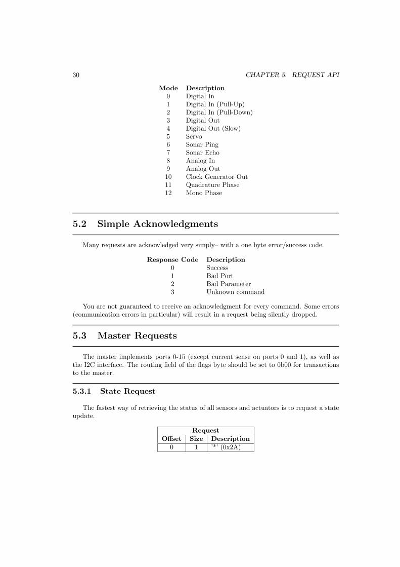
Mode Description0 Digital In1 Digital In (Pull-Up)2 Digital In (Pull-Down)3 Digital Out4 Digital Out (Slow)5 Servo6 Sonar Ping7 Sonar Echo8 Analog In9 Analog Out10 Clock Generator Out11 Quadrature Phase12 Mono Phase
5.2 Simple Acknowledgments
Many requests are acknowledged very simply– with a one byte error/success code.
Response Code Description0 Success1 Bad Port2 Bad Parameter3 Unknown command
You are not guaranteed to receive an acknowledgment for every command. Some errors(communication errors in particular) will result in a request being silently dropped.
5.3 Master Requests
The master implements ports 0-15 (except current sense on ports 0 and 1), as well asthe I2C interface. The routing field of the flags byte should be set to 0b00 for transactionsto the master.
5.3.1 State Request
The fastest way of retrieving the status of all sensors and actuators is to request a stateupdate.
RequestOffset Size Description
0 1 ’*’ (0x2A)
5.3. MASTER REQUESTS 31
ReplyOffset Size Description
3 1 ’*’ (0x2A)4 2 Low 16 bits of 512Hz clock6 2 Digital-in values (ports 0-15)8 2 Servo 0 PWM (port 0)10 2 Servo 1 PWM (port 1)12 2 Servo 2 PWM (port 2)14 2 Servo 3 PWM (port 3)16 2 Analog In 0 (port 8)18 2 Analog In 1 (port 9)20 2 Analog In 2 (port 10)22 2 Analog In 3 (port 11)24 2 Analog In 4 (port 12)26 2 Analog In 5 (port 13)29 2 Analog In 6 (port 14)30 2 Analog In 7 (port 15)32 2 Analog In 8 (port 0)34 2 Analog In 9 (port 3)36 1 Analog LPF 0-1 (ports 8-9)37 1 Analog LPF 2-3 (ports 10-11)38 1 Analog LPF 4-5 (ports 12-13)39 1 Analog LPF 6-7 (ports 14-15)40 1 Analog LPF 8-9 (ports 0, 3)41 1 Pin Modes 0-1 (ports 0-1)42 1 Pin Modes 2-3 (ports 2-3)43 1 Pin Modes 4-6 (ports 4-5)44 1 Pin Modes 6-7 (ports 6-7)45 1 Pin Modes 8-9 (ports 8-9)46 1 Pin Modes 10-11 (ports 10-11)47 1 Pin Modes 12-13 (ports 12-13)48 1 Pin Modes 14-15 (ports 14-15)49 2 Ultrasound Range 0 (port 5)51 2 Ultrasound Range 1 (port 7)53 1 Ultrasound Ping Count 0-1 (ports 5,7)54 1 Clock Generator Source55 1 Clock Generator Period56 1 Clock Generator Width57 1 DAC value58 4 Gyro Integrator (port 15)
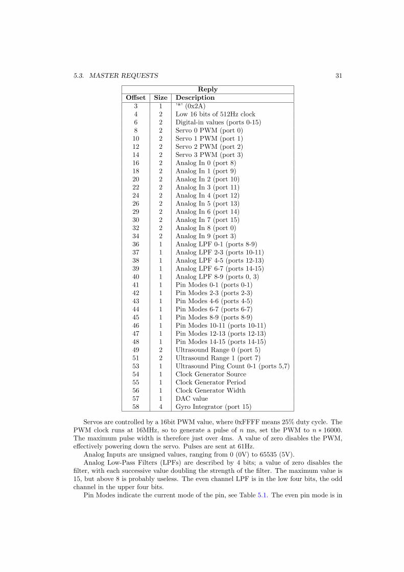
Servos are controlled by a 16bit PWM value, where 0xFFFF means 25% duty cycle. ThePWM clock runs at 16MHz, so to generate a pulse of n ms, set the PWM to n ∗ 16000.The maximum pulse width is therefore just over 4ms. A value of zero disables the PWM,effectively powering down the servo. Pulses are sent at 61Hz.
Analog Inputs are unsigned values, ranging from 0 (0V) to 65535 (5V).Analog Low-Pass Filters (LPFs) are described by 4 bits; a value of zero disables the
filter, with each successive value doubling the strength of the filter. The maximum value is15, but above 8 is probably useless. The even channel LPF is in the low four bits, the oddchannel in the upper four bits.
Pin Modes indicate the current mode of the pin, see Table 5.1. The even pin mode is in
32 CHAPTER 5. REQUEST API
the low four bits, the odd mode in the upper four bits.Ultrasound ranges are measured in intervals of a 1MHz clock.The Ultrasound Ping count is a a 4 bit rolling counter of how many times each ultrasound
port has been pinged, with channel 0 in the low four bits, channel 1 in the high four bits.The Gyro Integrator is a wrapping 32bit accumulator of the sum of the Analog In 7
(port 15) minus 32768, evaluated at 512Hz.
5.3.2 Analog Filter Set
Set the analog low-pass filter for a port.
RequestOffset Size Description
3 1 ’F’ (0x46)4 1 Filter value [0-15]
The response is a simple ack.
5.3.3 Configure Clock
Configure the programmable clock generator. Note: not implemented.
RequestOffset Size Description
3 1 ’K’ (0x4B)4 1 Source [0-15]5 1 Period [0-255]6 1 Width [0-255]
The response is a simple ack.
5.3.4 Configure Pin
Updates the digital out value for pins configured as a digital out.
RequestOffset Size Description
3 1 ’C’ (0x43)4 1 Digital pin number [0-15]5 1 Value [0, 1]
The response is a simple ack.
5.3.5 Digital Out Set
Updates the digital out value for pins configured as a digital out.
RequestOffset Size Description
3 1 ’D’ (0x44)4 1 Digital pin number [0-15]5 1 Value [0, 1]
The response is a simple ack.
5.3. MASTER REQUESTS 33
5.3.6 I2C Read
Perform an I2C Read transaction. (Note: not implemented)
RequestOffset Size Description
3 1 ’i’ (0x69)4 1 I2C Address5 1 length in bytes
RequestOffset Size Description
3 1 Result code4 length Data
5.3.7 I2C Write
Perform an I2C Write transaction. (Note: not implemented)
RequestOffset Size Description
3 1 ’I’ (0x49)4 1 I2C Address5 length Data to write
The response is a simple ack.
5.3.8 Servo Set
Change the value of the servo PWM.
RequestOffset Size Description
3 1 ’S’ (0x53)4 1 Servo number [0-3]5 2 PWM Value
The response is a simple ack.
5.3.9 Sonar Initiate
Send a pulse on the sonar channel’s pulse pin, then begin measuring the pulse widththat occurs on the channel’s echo pin. For channel 0, the pulse port is 4, echo is port 5. Forchannel 1, the pulse port is 6, echo is port 7.
RequestOffset Size Description
3 1 ’R’ (0x52)4 1 Sonar channel [0-1]
The response is a simple ack.
34 CHAPTER 5. REQUEST API
5.4 Slave Requests
The slave device is responsible for ports 16-19, the motors, and all the current-sensecapabilities on the board (including those on ports 0 and 1). The routing field of the flagsbyte should be set to 0b01 for transactions to the slave.
Motor directions come up in several transactions, and are encoded in two bits as follows:
Value Description0 Disabled (open circuit)1 Forward2 Reverse
Table 5.1: Motor Direction Constants
Braking can be accomplished by selecting either forward or reverse and selecting zeroPWM.
5.4.1 State Request
The fastest way of retrieving the status of all sensors and actuators is to request a stateupdate.
RequestOffset Size Description
3 1 0x2A
5.4. SLAVE REQUESTS 35
ReplyOffset Size Description
3 1 ’*’ (0x2A)4 1 Pin Modes 0-1 (ports 16-17)5 1 Pin Modes 2-3 (ports 18-19)6 1 Digital-in values of (ports 16-19)7 2 Quad/Mono-phase 0 (ports 16-17)10 1 Quad/Mono-phase 0 error count11 2 Quad/Mono-phase 1 (ports 18-19)12 1 Quad/Mono-phase 1 error count13 1 Motor 0 Goal PWM14 1 Motor 0 Actual PWM15 1 Motor 0 Slew16 1 Motor 1 Goal PWM17 1 Motor 1 Actual PWM18 1 Motor 1 Slew19 1 Motor 2 Goal PWM20 1 Motor 2 Actual PWM21 1 Motor 2 Slew22 1 Motor 3 Goal PWM23 1 Motor 3 Actual PWM24 1 Motor 3 Slew25 1 Motor Dir Goal/Actual 0-126 1 Motor Dir Goal/Actual 2-327 2 Analog In 0 (Motor Current 0)29 2 Analog In 1 (Motor Current 1)31 2 Analog In 2 (Motor Current 2)33 2 Analog In 3 (Motor Current 3)35 2 Analog In 4 (Port/Servo Current 0) (port 0)37 2 Analog In 5 (Port/Servo Current 1) (port 1)39 2 Analog In 6 (port 16)41 2 Analog In 7 (port 19)43 1 Analog In LPF 0-144 1 Analog In LPF 2-345 1 Analog In LPF 4-546 1 Analog In LPF 6-7
The formats for the pin modes and LPFs is identical to those on the master.The motor direction bytes encode both the desired (goal) and actual directions of the
motors. For the even-numbered channel, the goal direction is in the low two bits, and theactual direction is in bits 3 and 4. Data for the odd-channel is similarly stored in the highfour bits.
5.4.2 All Stop
Stops all motors as quickly as the slew rate allows. This is the command that is internallycalled when the emergency stop button is pressed.
RequestOffset Size Description
3 1 ’X’ (0x58)

36 CHAPTER 5. REQUEST API
The response is a simple ack.
5.4.3 Analog Filter Set
Identical to the master, except only channels [0,7] exist.
5.4.4 Configure Pin
Identical to the master, except only channels [0,3] exist.
5.4.5 Digital Out Set
Identical to the master, except only channels [0,7] exist.
5.4.6 Motor Set
Set the direction/speed motor.
RequestOffset Size Description
3 1 ’M’ (0x4D)4 1 Motor channel [0-3]5 1 Direction6 1 PWM
The response is a simple ack.
5.4.7 Motor Slew Set
Set the slew rate for a motor. The value is the maximum change in the PWM in 1/512second.
RequestOffset Size Description
3 1 ’W’ (0x57)4 1 Motor channel [0-3]5 1 Slew rate [1-255]
The response is a simple ack.
5.5 Pad Requests
The pad handles all LCD drawing/writing/reading functions, as well as reading thestatus of the joystick and buttons. The routing field of the flags byte should be set to 0b10for transactions to the OrcPad.
Two different types of text drawing are supported. One allows text to be arbitrarilypositioned on the screen, while the other implements “console”-type behavior, includingautomatic scrolling.
5.5. PAD REQUESTS 37
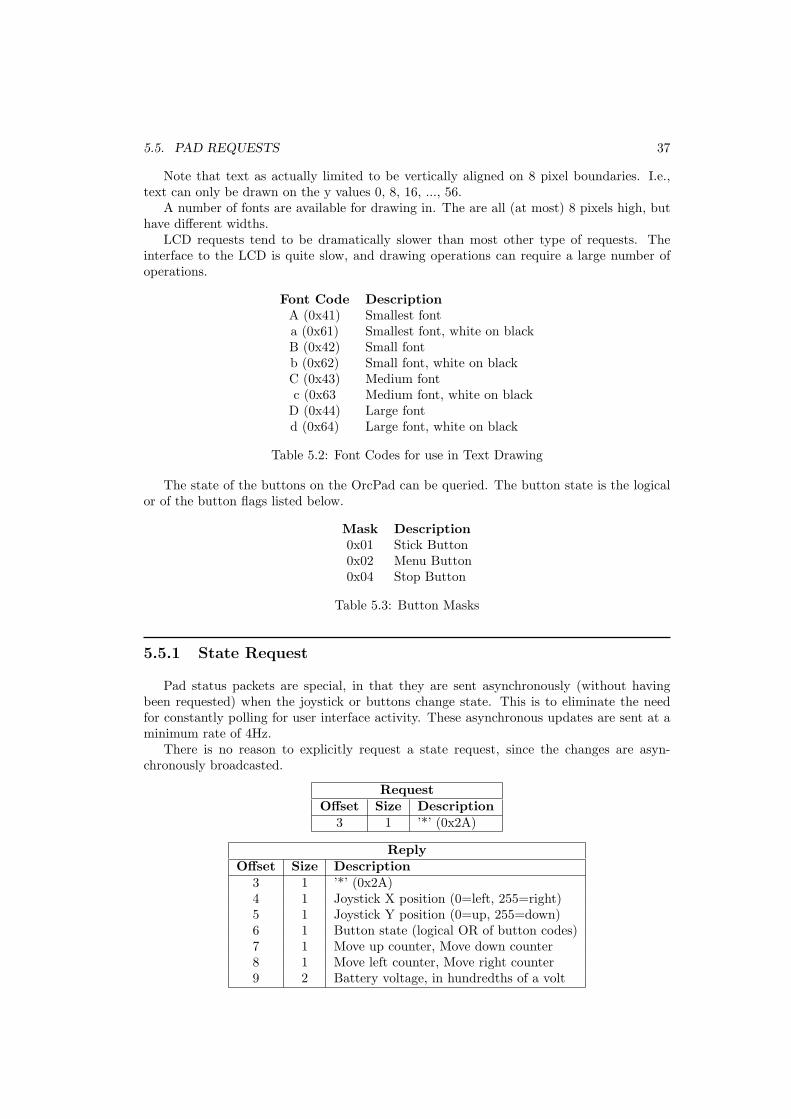
Note that text as actually limited to be vertically aligned on 8 pixel boundaries. I.e.,text can only be drawn on the y values 0, 8, 16, ..., 56.
A number of fonts are available for drawing in. The are all (at most) 8 pixels high, buthave different widths.
LCD requests tend to be dramatically slower than most other type of requests. Theinterface to the LCD is quite slow, and drawing operations can require a large number ofoperations.
Font Code DescriptionA (0x41) Smallest fonta (0x61) Smallest font, white on blackB (0x42) Small fontb (0x62) Small font, white on blackC (0x43) Medium fontc (0x63 Medium font, white on black
D (0x44) Large fontd (0x64) Large font, white on black
Table 5.2: Font Codes for use in Text Drawing
The state of the buttons on the OrcPad can be queried. The button state is the logicalor of the button flags listed below.
Mask Description0x01 Stick Button0x02 Menu Button0x04 Stop Button
Table 5.3: Button Masks
5.5.1 State Request
Pad status packets are special, in that they are sent asynchronously (without havingbeen requested) when the joystick or buttons change state. This is to eliminate the needfor constantly polling for user interface activity. These asynchronous updates are sent at aminimum rate of 4Hz.
There is no reason to explicitly request a state request, since the changes are asyn-chronously broadcasted.
RequestOffset Size Description
3 1 ’*’ (0x2A)
ReplyOffset Size Description
3 1 ’*’ (0x2A)4 1 Joystick X position (0=left, 255=right)5 1 Joystick Y position (0=up, 255=down)6 1 Button state (logical OR of button codes)7 1 Move up counter, Move down counter8 1 Move left counter, Move right counter9 2 Battery voltage, in hundredths of a volt
38 CHAPTER 5. REQUEST API
The move counters are continuously wrapping 4 bit counters of “synthetic” key events.If the joystick is held up for a short while, it generates an “up” event. This is analogousto a conventional keyboard’s auto-repeat. The OrcPad interprets all joystick movementsas possible up/down/left/right movements to simplify those users who desire that sort ofinterface, while simultaneously giving all applications the same “feel”. You can detect if abutton has been pressed by testing if the counter has changed value.
The move up and move down counters are stored in one byte, with “up” stored in thelow 4 bits, and “down” in the upper four bits. Similarly, “left” is stored in the low 4 bitsand “right” in the upper 4 bits.
5.5.2 Clear Display
Clear the display.
RequestOffset Size Description
3 1 ’C’ (0x43)
The response is a simple ack.
5.5.3 Console Goto Cursor
Clear the console and home the cursor.Request
Offset Size Description3 1 ’G’ (0x47)4 1 x position [0, 26]5 1 y position [0, 7]
The response is a simple ack.
5.5.4 Console Home Cursor
Clear the console and home the cursor.Request
Offset Size Description3 1 ’H’ (0x48)
The response is a simple ack.
5.5.5 Console Set Size
Set the size of the console “window”. Dimensions are in “characters”.Request
Offset Size Description3 1 ’S’ (0x53)4 1 top5 1 height6 1 left7 1 width
The response is a simple ack.
5.5. PAD REQUESTS 39
5.5.6 Console Write
Draw text at the current console position, wrapping and scrolling as necessary.
RequestOffset Size Description
3 1 ’W’ (0x57)4 (≤ 32) String
The response is a simple ack.
5.5.7 Draw Mode Set
Set the draw mode
RequestOffset Size Description
3 1 ’M’ (0x4D)4 1 The mode, 0=clear, 1=set, 2=xor
The response is a simple ack.
5.5.8 Draw Lines
Plot one or more lines in the current drawing mode. Lines are drawn from (xa, ya) to(xb, yb).
RequestOffset Size Description
3 1 ’L’ (0x4C)4 1 xa0
5 1 ya0
6 1 xb0
7 1 yb0
... ... ...4 + 4n + 0 1 xan
4 + 4n + 1 1 yan
4 + 4n + 2 1 xbn
4 + 4n + 3 1 ybn
The response is a simple ack.
5.5.9 Draw text
Draw text at a random location in a user-definable font.
RequestOffset Size Description
3 1 ’T’ (0x54)4 1 x5 1 y6 1 font code7 (≤ 32) String
40 CHAPTER 5. REQUEST API
5.5.10 Draw top text
Draw text on the top line.
RequestOffset Size Description
3 1 ’t’ (0x74)4 1 x5 (≤ 32) String
The response is a simple ack.
5.5.11 Draw Pixels
Plot one or more pixels in the current drawing mode.
RequestOffset Size Description
3 1 ’P’ (0x50)4 1 x0
5 1 y0
... ... ...4 + 2n + 0 1 xn
4 + 2n + 1 1 yn
The response is a simple ack.
5.5.12 Fill Display
Fill the display with a pattern, x=even columns, y=odd columns. For example, to fillwith a checkerboard pattern, use x=0x55, y=0xAA. To fill with vertical stripes, x=0xFF,y=0x00. To fill with horizontal stripes, x=0x55, y=0x55.
RequestOffset Size Description
3 1 ’F’ (0x46)4 1 even column value5 1 odd column value
The response is a simple ack.
5.5.13 Raw read
Read the LCD’s frame buffer in a horizontal swath, 8 columns high. See Appendix Bfor more information.
RequestOffset Size Description
3 1 ’r’ (0x72)4 1 x5 1 y6 1 length ≤ 32

5.5. PAD REQUESTS 41
ReplyOffset Size Description
3 1 result code4 length data
5.5.14 Raw write
Write the LCD’s frame buffer in a horizontal swath, 8 columns high. See Appendix Bfor more information.
RequestOffset Size Description
3 1 ’R’ (0x52)4 1 x5 1 y6 (≤ 32) data
The response is a simple ack.

42 CHAPTER 5. REQUEST API

Appendix A
Soldering and PCB Assembly
To a beginner, soldering can seem very simple: melt some metal “glue” to join two othermetal bits together. However, glue is not glue. Creating a good solder joint–one which isboth electrically and mechanically reliable– is a function of chemistry and technique.
A.1 Chemistry and Metallurgy of Soldering
In a piece of metal, the metal atoms form metallic bonds. In this state, an electron is notassociated with any particular atom, but is free to move around the metal. This freedom ofmobility is what gives metals such good electrical and thermal conductivity.
When building circuits, we often want to join together two smaller bits of metal, makinga good thermal/electrical/mechanical connection. In other words, we want to make the twopieces of metal act as though they were a single piece.
There are two main enemies of a good metal joint. The first is oxidation: instead offorming metallic bonds, the metal atoms form ionic bonds with oxygen atoms. In thesemolecules, electrons are tightly bound to their molecule. Electrons can’t move, and poorconductivity results.
The second enemy of a good metal joint is a poor mechanical linkage. Not only shouldthe two metals be as physically close as possible, but there should be no sudden changesin the composition/properties of the material when moving from one piece of metal to thenext piece. When the interface between two different materials occurs over a very smalldistance, a poor mechanical linkage results. These interfaces act like cracks in a crystal.
One approach to joining bits of metal is to melt the two bits and let them cool together.This makes a terrific joint. But the melting point of copper is 1084 degrees Celsius, makingthis an impractical approach.
The goal of soldering is to join bits of metal by using an intermediary metal that has alow melting point. For example, typical tin/lead solder melts at around 350 degrees Celsius.Of course the solder will fill gaps and spaces between the two pieces. More importantly,however, when the bits of metal are heated as well, the solder will diffuse into the bits ofmetal. When it does this, it forms an alloy where the concentration of the bit of metal andsolder gradually changes. The result is a stronger mechanical connection.
The metals used in electronics oxidize in the presence of oxygen, forming a “skin” layerwhich has poor conductivity. When soldering, this layer must be removed. The solution isflux, an acid which reduces the metallic oxides to metallic salts and water which then flowaway from the joint.
Most solder comes with flux mixed in. Flux can be any of a number of chemicals, butis often an organic carboxylic (R-COOH) acid. The “smoke” you see when soldering is
43
44 APPENDIX A. SOLDERING AND PCB ASSEMBLY
actually a result of the flux burning, and contains very little metal. The burning of the fluxalso helps to remove oxygen immediately around the joint, which helps to prevent oxidationin the joint itself.
Fluxes which use organic acids leave residue on the PCB which, depending on the sever-ity, may need to be removed using a solvent. “No-clean” fluxes are available which typicallyperform quite poorly, but they do not require cleaning.
Key points:
• Both the solder and the metal it is being applied to must be heated, in order foran alloy to form. “Cold joints” can be difficult to detect visually, so they must beprevented through good technique.
• The joint must be free of oxidation. Oxidation is often easy to spot; it results in a dull,lumpy, or “rusty” appearance. A good joint should always appear clean and lustrous.
A.2 Soldering Tools
Achieving high quality soldering results requires a number of tools. Good quality toolscan very quickly pay for themselves by making it possible to work much more quickly andefficiently.
A basic set of tools consists of:
• A high-quality soldering iron. If the iron costs less than $40, it is almost certailygarbage. Good irons typically cost at least $100. If that sounds like a lot, considerthe value of your time and that making a joint with a lousy iron– if possible at all–can easily take many times longer. Weller’s WESD-51D and WLC-100 are both fineirons.
• Several sizes of rosin-core flux. For fine electronics work (e.g., SMT devices), use thinsolder (0.015-0.025 inch diameter): it gives you a great amount of control over howmuch solder is being applied. On larger soldering jobs (such as rows of DIPs or powerconnectors), thicker solder (0.050 inch diameter) is less tedious to apply. The soldermust have flux; I prefer solders with a greater amount of flux (3.3%). Additional fluxmakes the solder flow better, but the additional residue left on the board can requirecleaning in order to get a “professional” look.
• Solder removing device(s). There are two basic types: solder suckers and solder braid,each preferred by different folks. I vastly prefer solder suckers. With both devices,the trick to removing solder is that you often need to add solder first, so that there’senough thermal conductivity to melt the entire chunk of solder at once.
• Tweezers, preferrably normally-closed. When working on two-terminal SMD devices,tweezers are a must. Tweezers which are normally-closed will be much less tiring touse.
• Flux pen. Particularly when working on fine-pitch components, adding a little fluxcan make the solder flow much better. Or, when solder has been overworked and isbeginning to oxidize, it is helpful to be able to add a bit more flux.
• A “helping hand” unit, basically two alligator clips on positionable arms, can be veryhelpful when making cables.
A.3. ASSEMBLY STRATEGY 45
• An anti-static mat and wrist-band. After assembling a board, it’d be unfortunate itif got zapped before you even got a chance to use it!
• Fume extractor. Flux fumes can irritate the respiratory tract, so if doing a lot ofsoldering, using a fume extractor is a good idea. Inexpensive units, consisting of littlemore than a fan to suck the exhaust with an activated carbon filter, are available forunder $30.
A.3 Assembly Strategy
Planning your assembly process in advance, and staying organized, will greatly assistassembly. Here are some basic tips:
• Start with the shortest/smallest components first. This will help the board lay flat,making it easier to keep components in position while assembling them.
• Add through-hole devices in batches. Gently bending the leads on electroylitic capac-itors will prevent them from falling out. Then you can solder them all at once. It’soften helpful to “tack” each capacitor in position with just one lead; then the tackedpin can be reflowed and the capacitor pushed flush to the board.
• Keep the iron tip clean with a sponge or tip cleaner. The tip should be smooth andlustrous. It should also be “primed” with a small amount of solder; this will aidthermal conduction to joints. If the tip is severely soiled, adding flux will often help.Never sharpen or slice off oxidation from the tip; it will ruin the tip!
• Use moderate iron temperatures. High temperatures can damage components. Formost board work, a temperature of 650 degrees should be sufficient.
• Somewhat paradoxically, the best soldering results come from work that is performedquickly (i.e., where the length of time that solder is liquefied is minimized.) Painstak-ingly applying and “working” solder is doomed to produce heavily oxidized joints. Ofcourse, it takes some practice to learn how to move quickly.
When your soldering technique is developed, you’ll find that solder acts like a liquid withpretty high surface tension. This surface tension does most of the work for you– if you putsolder near a joint, it will flow onto the joint and cover it.
A.4 Making Cables
A surprisingly difficult problem in practical electrical enginnering is how to connecttwo devices. There are several features which someone might look at when selecting acable/connector system:
• Mechanical Robustness. The connectors stay connected, and the connector/cable willnot fatigue and break.
• Polarization. The connector can only be inserted one way, eliminating the risk ofdamaging equipment.
• Inexpensive.
46 APPENDIX A. SOLDERING AND PCB ASSEMBLY
• Physical Size. Depending on the application, an easily manipulatable (large) connectormight be preferrable, or density might be an issue, where fitting the maximum numberof connectors per unit area is critical.
• Electrical Properties. Current carrying capacity, parasitic inductance, capacitance,resistance, can all be important in some situations. Motor connectors, for example,should be able to carry more power than a simple push button.
The OrcBoard has a lot of sensor connectors, so an inexpensive and physically smallconnector are used predominantly. These connectors are constructed from 0.100” maleand female header. These connectors are not polarized (though the distinctive pattern ofPin-Pin-Blank-Pin is intended to make it easy to discern the correct polarization.)
It takes a fair amount of practice to produce reliable cables using 0.100” header, andseveral steps are required (see Fig. A.4). Of critical importance is the use of stranded, ratherthan solid wire. Solid wire fatigues very rapidly with mechanical stress, whereas strandedwire is much more robust.
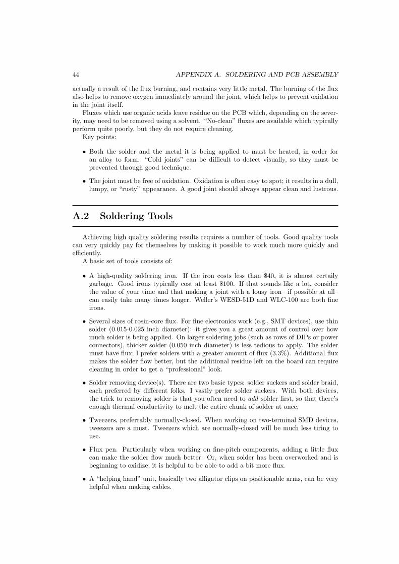
(a) (b) (c) (d) (e)
(f ) (g) (h)
Figure A.1: Making Cables. Beginning with stranded ribbon cable (a), separate the leadsabout 1” (b). Strip about 0.25” from each lead and lightly twist together the stranded wires(c). Tin the ends of the wire and the connector (d), then slip on 0.3” lengths of heatshrinktubing onto each wire (e). Join the wires and the header (f), adding more solder if necessary.Position the heatshrink tubing and heat it (g). For added structural strength, apply hotglue to the connector (h).
Notice that virtually every connector on the OrcBoard has “ground” on the outside ofthe board. The convention of OrcBoard cables is to call the ground wire “pin 1”, and tocolor that wire to designate it as such. The color coding thus provides a polarization cue:the colored wire should be on the outside of the board.
A.5. ASSEMBLING THROUGH-HOLE DEVICES 47
An option to those who loathe assembling cables as described in this section is to usefemale crimp connectors. The sensors connectors (now female) are then attached to theOrcBoard (also female) by using a coupler created from wire-wrap male header.
A.5 Assembling through-hole devices
The OrcBoard contains a substantial number of through-hole components, mostly in anattempt to maximize the number of parts which are socketed (and can be easily replaced ifthey fail.)
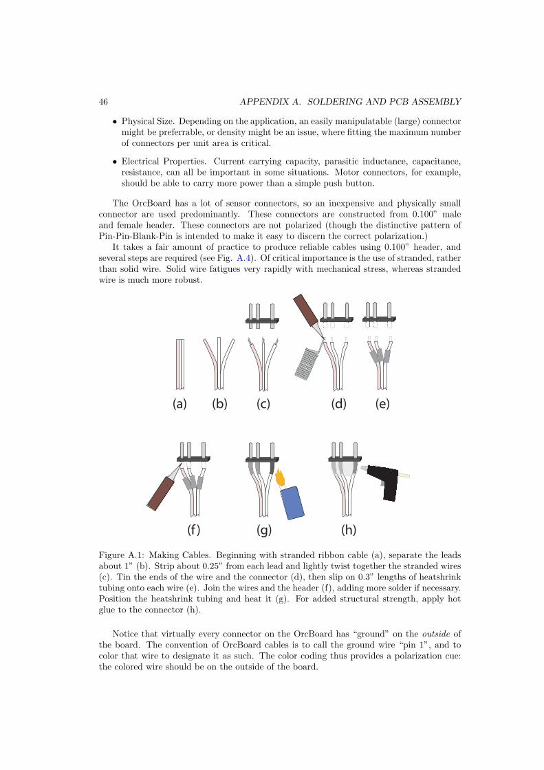
The steps for assembling a through-hole part are shown in Fig. A.5. Making sure thatthe part is flush with the board is important for both cosmetic and signal integrity reasons.The best way to mount components so that they are flush is to tack down one pin, thenreflow that pin while pushing the part flush to the board. Then, tack down the other pins.
(a) (b) (c)
(d) (e) (f) (g)
Bad Joints
Figure A.2: Through-hole Soldering. Beginning with an unsoldered connection (a), addsolder while heating both the pin and the pad (b). When finished, the joint should beconical and lustrous (c). Joint (d) doesn’t have enough solder; often only a thin membraneof solder is in place, and the joint is very weak. A common result of heating the pin butnot the pad is (e), known as a “lollipop joint”. These joints can be difficult to spot, sincethe solder on the pin conceals the missing connection to the pad. Joint (f) shows signs ofoxidation: the solder has become sticky and is too thick; it also shows a little “tail”. Thesejoints are usually functional, if unattractive. Joint (g) is grotesquely oxidized; the solderhas become sludgy and is on far too thick. Adding additional flux and reflowing might fixthe joint, but removing the solder and starting over can be necessary.
Be especially aware of “lollipop joints”, a joint where solder has only adhered to the pinand not to the pad. It is caused by not heating the pad with the iron. These joints can behard to see when they do occur, because the solder attached to the pin makes it hard to seewhether there is a connection to the pad.
A.6 Assembling SMT devices
Two-terminal SMT devices, including capacitors and resistors, are easy to assemble and
48 APPENDIX A. SOLDERING AND PCB ASSEMBLY
take up little board space. In the case of resistors, it is also easier to read the value of theresistor (which is printed in ordinary numerals on the package): the last digit is typicallythe power of 10, so “1202” means 120 ∗ 102, or 12k.
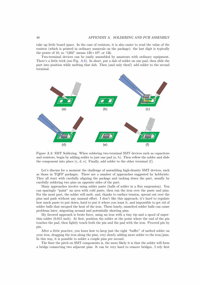
Two-terminal devices can be easily assembled by amateurs with ordinary equipment.There’s a little trick (see Fig. A.6). In short, put a dab of solder on one pad, then slide thepart into position while melting that dab. Then (and only then!) add solder to the secondterminal.
R333
R333 R333 R333
(a)
(d)
(b)
(e)
(c)
(f)
Figure A.3: SMT Soldering. When soldering two-terminal SMT devices such as capacitorsand resistors, begin by adding solder to just one pad (a, b). Then reflow the solder and slidethe component into place (c, d, e). Finally, add solder to the other terminal (f).
Let’s discuss for a moment the challenge of assembling high-density SMT devices, suchas those in TQFP packages. There are a number of approaches suggested by hobbyists.They all start with carefully aligning the package and tacking down the part, usually bycarefully soldering two pins on opposite sides of the part.
Many approaches involve using solder paste (balls of solder in a flux suspension). Youcan sparingly “paint” an area with cold paste, then run the iron over the paste and pins.For the most part, the solder will melt, and, thanks to surface tension, spread out over thepins and pads without any manual effort. I don’t like this approach; it’s hard to regulatehow much paste to put down, hard to put it where you want it, and impossible to get rid ofsolder balls that escaped the heat of the iron. These lonely, unmelted solder balls can causeproblems later, migrating around and potentially shorting pins.
My favored approach is brute force, using an iron with a tiny tip and a spool of super-thin solder (0.015 inch). At first, position the solder at the point where the end of the pintouches the pad, then lightly touch both the pin and the pad with the iron. Proceed pin bypin.
After a little practice, you learn how to keep just the right “buffer” of melted solder onyour iron, dragging the iron along the pins, very slowly adding more solder to the iron/pins.In this way, it is possible to solder a couple pins per second.
The finer the pitch on SMT components is, the more likely it is that the solder will forma bridge connecting two adjacent pins. It can be very hard to remove bridges. I rely first

A.6. ASSEMBLING SMT DEVICES 49
and foremost on a flux pen (to keep the solder flowing easily) and a solder sucker. But incases where you’ve really made a mess, a dental pick to scrape molten solder from the pinscan be a help.
I consider a stereo microscope essential with parts finer than TQFP44, and I generallyconsider TQFP144s the upper-limit of what can/should be assembled without specializedequipment.

50 APPENDIX A. SOLDERING AND PCB ASSEMBLY
Appendix B
LCD Memory Map
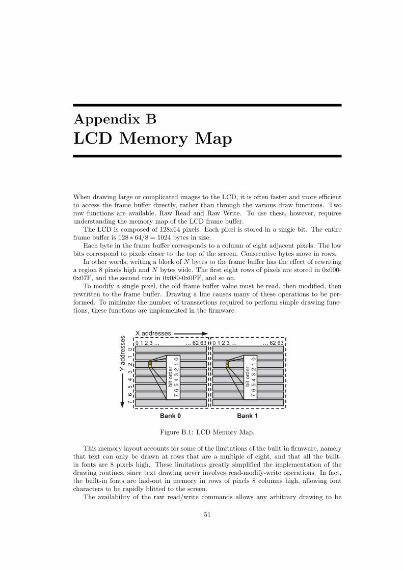
When drawing large or complicated images to the LCD, it is often faster and more efficientto access the frame buffer directly, rather than through the various draw functions. Tworaw functions are available, Raw Read and Raw Write. To use these, however, requiresunderstanding the memory map of the LCD frame buffer.
The LCD is composed of 128x64 pixels. Each pixel is stored in a single bit. The entireframe buffer is 128 ∗ 64/8 = 1024 bytes in size.
Each byte in the frame buffer corresponds to a column of eight adjacent pixels. The lowbits correspond to pixels closer to the top of the screen. Consecutive bytes move in rows.
In other words, writing a block of N bytes to the frame buffer has the effect of rewritinga region 8 pixels high and N bytes wide. The first eight rows of pixels are stored in 0x000-0x07F, and the second row in 0x080-0x0FF, and so on.
To modify a single pixel, the old frame buffer value must be read, then modified, thenrewritten to the frame buffer. Drawing a line causes many of these operations to be per-formed. To minimize the number of transactions required to perform simple drawing func-tions, these functions are implemented in the firmware.
bit o
rder
7 6
5 4
3 2
1 0
0 1 2 3 … … 62 63
7
6
5 4
3
2
1
0
Y
ad
dre
sse
s
X addresses
Bank 0
bit o
rder
7 6
5 4
3 2
1 0
0 1 2 3 … … 62 63
Bank 1
Figure B.1: LCD Memory Map.
This memory layout accounts for some of the limitations of the built-in firmware, namelythat text can only be drawn at rows that are a multiple of eight, and that all the built-in fonts are 8 pixels high. These limitations greatly simplified the implementation of thedrawing routines, since text drawing never involves read-modify-write operations. In fact,the built-in fonts are laid-out in memory in rows of pixels 8 columns high, allowing fontcharacters to be rapidly blitted to the screen.
The availability of the raw read/write commands allows any arbitrary drawing to be
51

52 APPENDIX B. LCD MEMORY MAP
performed. Despite the fact that the display is monochrome, video can be displayed in areasonably intelligent way, provided that the frame is redrawn fast enough ( 8 Hz) to achievesome “temporal dithering.”
In truth, the frame buffer is somewhat more complicated; the left half of the screen isaddressed independently of the right half of the screen, and there are in fact two distinctframe buffers. However, this complexity is handled by the OrcPad firmware.

Appendix C
The OrcPad as a PrototypingBoard
The OrcPad can be used as a standalone prototyping board. It contains a DB-9 connectorand a RS-232 charge pump that, when populated, allow the OrcPad to be directly connectedto a host without an OrcBoard.
The OrcPad can use either the 128x64 pixel LCD, or a character LCD module, such asthe CFAH1602B. The graphical LCD panel uses a large number of pins; using a charactermodule frees up some of those pins, allowing them to be used to implement other features.Note that the character module and graphical module cannot be used at the same time, andalso that they require separate contrast adjustment potentiometers.
Ordinarily, the OrcPad receives its power from the OrcBoard. In a standalone applica-tion, the OrcPad can receive its power from a wall adapter (a power jack is provided) anda 5V linear regulator. If a regulated 5VDC wall adapter is used, then the 5V regulator isunnecessary; simply short pins 1 and 3 with a short piece of wire.
53

54 APPENDIX C. THE ORCPAD AS A PROTOTYPING BOARD

Appendix D
Orcd, The Orc CommunicationsManager
In simple applications, a single application will connect to the OrcBoard (see Fig. D). Theseapplications have exclusive access to the OrcBoard.
COM Port
Application
Figure D.1: System without Orcd. In simple systems, a single application communicatesdirectly with the OrcBoard.
In many applications, it is convenient for many applications to access the same OrcBoard.Orcd allows multiple applications to share an OrcBoard. Applications access orcd via TCPsockets. Orcd implements the following features:
• Allows multiple applications to connect and issue transactions to the OrcBoard. Re-sponses generated by other applications are automatically filtered out.
• Assigns new transaction IDs to all requests (and their responses) so that requestsfrom multiple applications do not collide. Each packet is transparently rewritten,so that the response packet’s transaction ID received by an application matches thetransaction ID used in the application’s request.
• Provides a simple synchronous interface for requests/responses. Each connection tocommand port (TCP port 7320) allows a single outstanding request, and is guaranteedto send either the Orc’s response or a timeout error packet. An application can supportmultiple simultaneous transactions by connecting more than once. This makes writingan application much easier.
• Automatically polls the master and slave for state update requests, and publishes theresults to the asynchronous event port (TCP port 7321). A client can enter a simpleinfinite read loop to receive these packets. Use of this feature conserves OrcBoardbandwidth since all applications can share the same state update information.
55
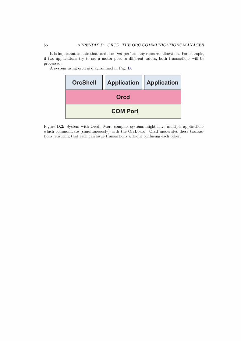
56 APPENDIX D. ORCD, THE ORC COMMUNICATIONS MANAGER
It is important to note that orcd does not perform any resource allocation. For example,if two applications try to set a motor port to different values, both transactions will beprocessed.
A system using orcd is diagrammed in Fig. D.
COM Port
Application ApplicationOrcShell
Orcd
Figure D.2: System with Orcd. More complex systems might have multiple applicationswhich communicate (simultaneously) with the OrcBoard. Orcd moderates these transac-tions, ensuring that each can issue transactions without confusing each other.
Appendix E
Firmware Overview
The firmware used on the OrcBoard and OrcPad is available under the GPL license. Itis available under other licenses by contacting the copyright owner (Edwin Olson, [email protected]). The firmware is a mix of PSoC/M8C assembly and C.
By modifying the firmware, not only can you fix bugs, but you can add new features. The“basic” firmware that ships with the OrcBoard tries to be a “Swiss Army Knife”, providinga bit of everything. But many specialized robots will need more specialized functionality.For example, the firmware could be changed to support a dozen servos, at the expense ofsome of the other built-in features.
When implementing new commands,keep in mind the nature of the packet-based mes-saging system. Packets may be lost, so commands and responses which are idempotentare desirable whenever possible. For example, rather than implementing “Increase MotorSpeed”, implement “Set Motor Speed”. If an acknowledgment is not received by the userafter sending an “increase” command, there’s no way of knowing whether the request wasreceived, whether it was executed, or whether the acknowledgment was lost. If it retrans-mits, it might effectively increase the motor speed twice. Clearly, a “set” function does nothave this problem.
This chapter will describe some of the common design patterns in the firmware, as wellas explaining a few of the “tricks” that were used. A basic familiarity with PSoCs will beassumed.
E.1 Pin Reconfiguration
Many pins on the OrcBoard have multiple functions. This is accomplished in a straight-forward way in the firmware. In almost every case, any given pin can only be in one ofthree modes: a digital in/out pin, an analog in/out pin, or a single “special” function. Thespecial modes change for each pin, but include all those modes which use a digital block:servos, sonar echo, PWM, etc.
Using the PSoC’s internal routing, the digital blocks which implement each pin’s specialfunction are statically routed to their pin. When switching the mode of a pin to the specialfunction, only a single configuration bit needs to be changed.
E.2 Interrupts and Performance
The firmware is written for high performance, low latency, and maximum throughput.Serial read and write operations are all performed via interrupt-driven queues. This way,
57
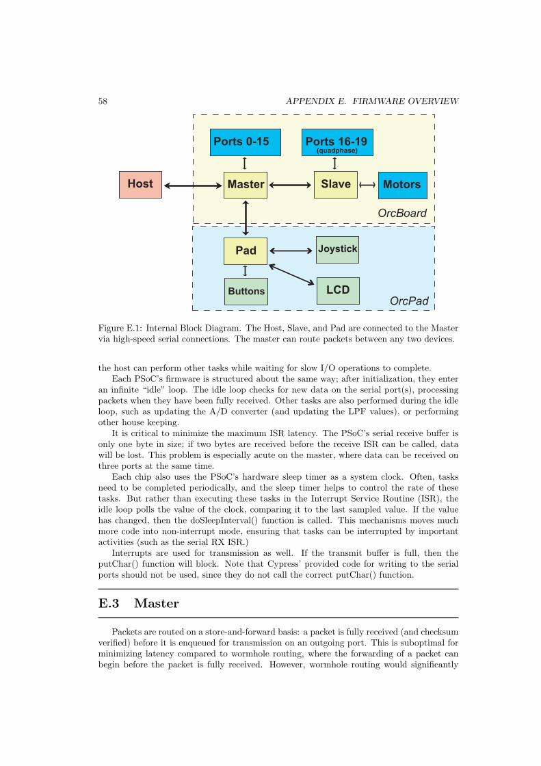
58 APPENDIX E. FIRMWARE OVERVIEW
Host Master Slave
Pad
LCD
Joystick
Ports 0-15 Ports 16-19
Motors
(quadphase)
OrcBoard
OrcPadButtons
Figure E.1: Internal Block Diagram. The Host, Slave, and Pad are connected to the Mastervia high-speed serial connections. The master can route packets between any two devices.
the host can perform other tasks while waiting for slow I/O operations to complete.Each PSoC’s firmware is structured about the same way; after initialization, they enter
an infinite “idle” loop. The idle loop checks for new data on the serial port(s), processingpackets when they have been fully received. Other tasks are also performed during the idleloop, such as updating the A/D converter (and updating the LPF values), or performingother house keeping.
It is critical to minimize the maximum ISR latency. The PSoC’s serial receive buffer isonly one byte in size; if two bytes are received before the receive ISR can be called, datawill be lost. This problem is especially acute on the master, where data can be received onthree ports at the same time.
Each chip also uses the PSoC’s hardware sleep timer as a system clock. Often, tasksneed to be completed periodically, and the sleep timer helps to control the rate of thesetasks. But rather than executing these tasks in the Interrupt Service Routine (ISR), theidle loop polls the value of the clock, comparing it to the last sampled value. If the valuehas changed, then the doSleepInterval() function is called. This mechanisms moves muchmore code into non-interrupt mode, ensuring that tasks can be interrupted by importantactivities (such as the serial RX ISR.)
Interrupts are used for transmission as well. If the transmit buffer is full, then theputChar() function will block. Note that Cypress’ provided code for writing to the serialports should not be used, since they do not call the correct putChar() function.
E.3 Master
Packets are routed on a store-and-forward basis: a packet is fully received (and checksumverified) before it is enqueued for transmission on an outgoing port. This is suboptimal forminimizing latency compared to wormhole routing, where the forwarding of a packet canbegin before the packet is fully received. However, wormhole routing would significantly
E.4. SLAVE 59
complicate the firmware.
E.4 Slave
The slave’s most interesting feature is the quadrature phase decoder ISR. Configured torun whenever the General Purpose I/O (GPIO) pins change state, they implement a statemachine. The state is the last sampled value of the two quadrature phase pins, and theinput is the new value of the two pins. A lookup table is used to branch to an appropriateroutine, which increments/decrements the counter, or increments the error counter if anillegal transition was detected. This process is repeated for both quadrature phase channels.
The ports are reconfigured to perform simple (monophase) decoding by simply using adifferent lookup table.
The slave is also responsible for implementing the PWM slewing function. When thesystem timer (implemented by the sleep counter) changes, the PWM values of each motorchannel are updated. (Actually, the system clock runs at 512Hz, and PWM are only updatedevery fourth time yielding an update rate of 64Hz.)
Implementing the motor PWM modules required exploiting the PSoC’s digital Look-Up-Tables (LUTs). Each motor is controlled by three pins: an enable pin, and two controlpins (call them A and B). To drive forward or backward, the enable pin must be set.Driving forward is accomplished by setting A=PWM and B=0, while driving backwards isaccomplished by setting A=0 and B=PWM. Each motor’s PWM signal is routed to twoLUTs. These LUTs can then be set to follow the PWM signal or to be the constant value0. Changing the LUTs allows the direction to be changed.
E.5 Pad
The Pad’s chief responsibility is managing the LCD and updating measurements of thetwo analog joystick axes and the three binary push buttons.
In addition, it monitors the battery voltage so it can be displayed on the LCD. This isdone on the Pad instead of the OrcBoard in order to avoid the need for the pad to query themaster/slave for the voltage, and also because the pad’s PSoC had an extra pin left over,whereas pins were very scarce on the master and slave.
A powerful feature of the pad is its ability to generate synthetic cursor events. Thejoystick is monitored for movement up, down, left, and right; when enough movement hasoccurred, a discrete “key press” is generated. If the joystick is held in a particular direction,additional discrete key presses are generated, much like a keyboard’s auto-repeat function.This feature is implemented by integrating the joystick’s deviation in the X and Y direction,and comparing the integrated value to particular thresholds. This feature simplifies thedesign of other applications which are more easily described in terms of key presses thanjoystick movement, while giving all such applications the same “feel.”
Uniquely, the pad will send state update messages without having been requested to doso. When the discrete buttons change state, or the joystick state changes by a threshold,a new packet is scheduled for transmission (the needUpdate flag is set.) However, the rateat which these unsolicited packets are sent is limited to about 110 Hz, in order to preventthem from consuming an excessive amount of bandwidth.
The unsolicited messages are designed so that applications do not need to rapidly pollthe pad for user input; the applications can simply go to sleep and wait for the pad toannounce that an event has occurred.

60 APPENDIX E. FIRMWARE OVERVIEW

Appendix F
Schematics
The schematics are available in electronic format for Mentor Graphics PADs PowerLogicand PowerPCB.
F.1 Design Notes
F.1.1 Conventions
A general goal was to reduce component count in order to make assembly easier. Compo-nents with integrated passives are used whenever available. For example, the RS-232 chargepump is the more expensive MAX233E, which includes the passive capacitors. LEDs, pleasenote, are always LEDs with built-in current limiting resistors; do not substitute a conven-tional LED!
F.1.2 Power Supply
The switching power supply was obtained by using National’s online “Web Bench” ap-plication. The supply is rated for 5A. The high switching frequency is important for rapidlydealing with transients. An earlier version of the OrcBoard with a slower switching supplysuffered from brownouts with load transients.
F.1.3 Motor Drivers
The two motor drivers share a single charge pump circuit, as described by the L6205Napplication note.
F.1.4 Cut Header
To populate an OrcBoard and OrcPad, the following header will need to be cut:
61
62 APPENDIX F. SCHEMATICS
Type Size Qty per kitRight-angle Male 5 x 2 2
Male 20 x 1 1Female 20 x 1 1Female 8 x 1 1Female 5 x 1 2Female 8 x 2 3Female 4 x 2 3
F.1.5 Communications
The USBMOD3, manufactured by Elexol, can be mounted in the DIP32 (0.6”) landingon the OrcBoard, providing a USB interface to the OrcBoard. There is only enough roomfor either the DB-9 and RS-232 chargepump or the USBMOD3, so only one can be used atonce.
When using RS-232, a TX and RX LED are available. These are powered directly fromthe TX and RX signals themselves, so the sources of these signals must be strong enough todrive an LED while maintaining adequate rise/fall times. The PSoC can drive the TX pinadequately, and the MAX233 charge pump can drive the RX pin adequately. However, theUSBMOD3 cannot drive the RX pin, so the RX LED must not be used with the USBMOD3.A dedicated LED is available for the USBMOD3; it should be used instead.
F.2 OrcBoard Schematics
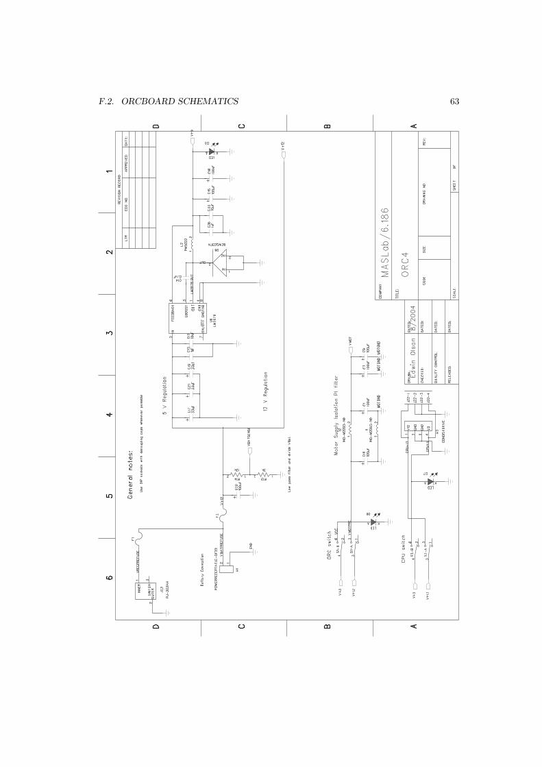
F.2. ORCBOARD SCHEMATICS 63
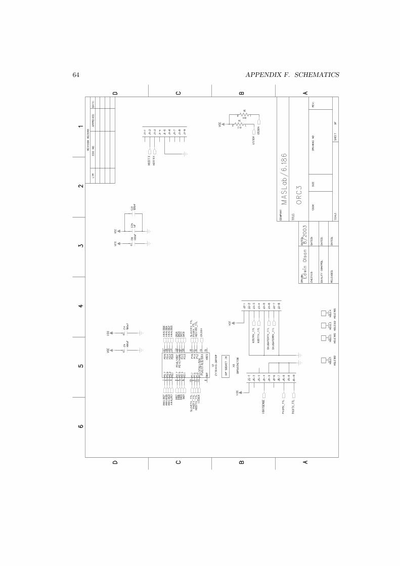
64 APPENDIX F. SCHEMATICS
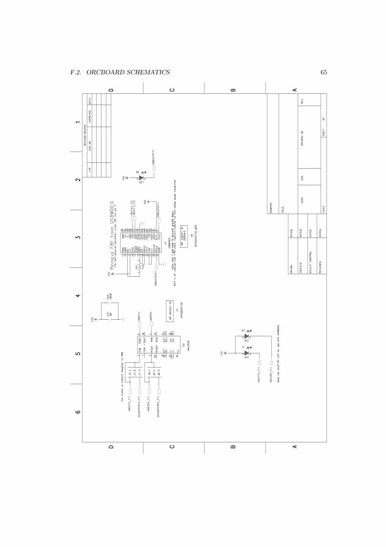
F.2. ORCBOARD SCHEMATICS 65
66 APPENDIX F. SCHEMATICS
F.2. ORCBOARD SCHEMATICS 67
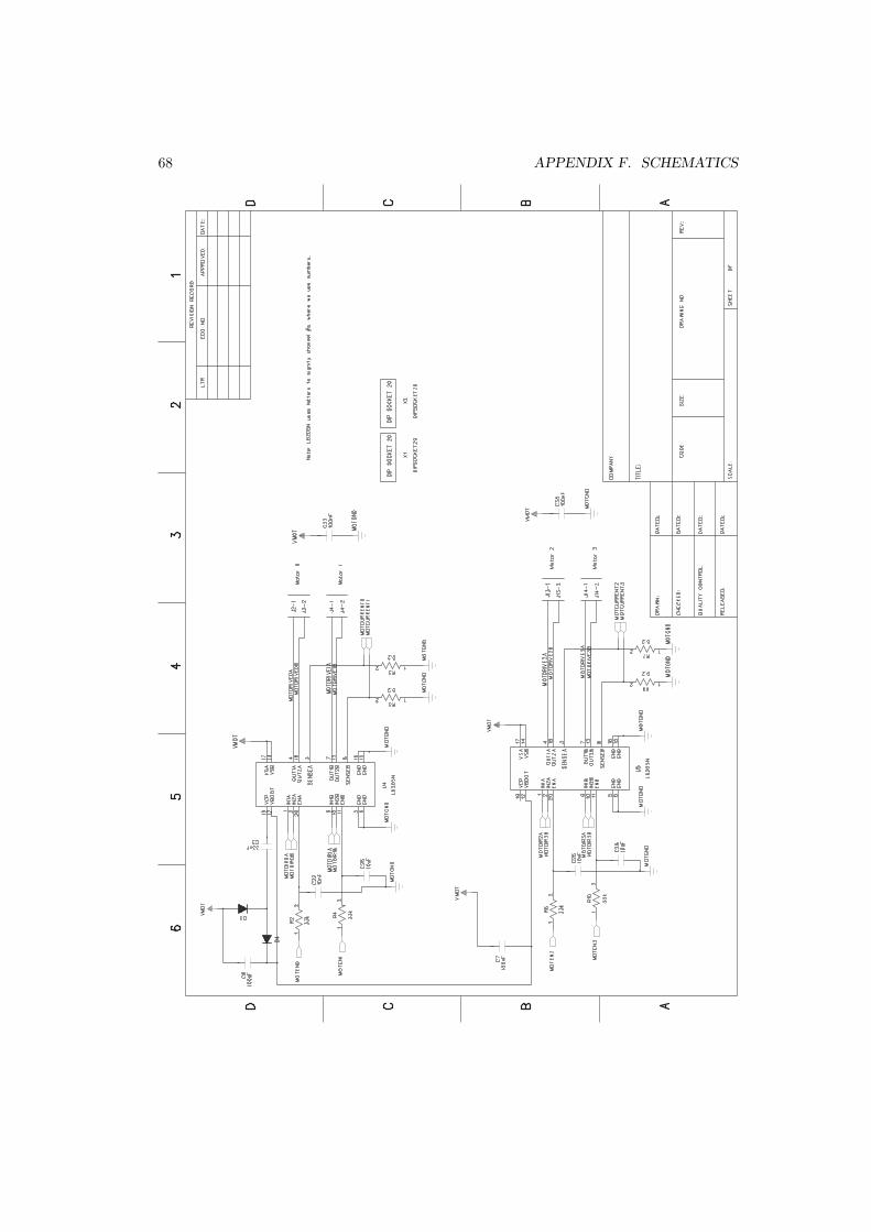
68 APPENDIX F. SCHEMATICS

F.3. ORCPAD SCHEMATICS 69
F.3 OrcPad Schematics
70 APPENDIX F. SCHEMATICS
F.3. ORCPAD SCHEMATICS 71
72 APPENDIX F. SCHEMATICS