Embed Size (px)
Citation preview
JOURNAL OF SEMICONDUCTOR TECHNOLOGY AND SCIENCE, VOL.17, NO.5, OCTOBER, 2017 ISSN(Print) 1598-1657 https://doi.org/10.5573/JSTS.2017.17.5.729 ISSN(Online) 2233-4866
Manuscript received Jun. 7, 2017; accepted Sep. 19, 2017 1 School of Electronics and Computer Engineering, Chonnam National University, Gwangju, 500-757, Korea 2 Department of Electrical and Control Engineering, Mokpo National University, Jeollanam-do, 534-729, Korea 3 School of Electrical Engineering, Seoul National University, Seoul, 151-742, Korea 4 The KEPCO Research Institute, Daejeon, 305-760, Korea E-mail : [email protected]
The Optimized Partial Insulator Isolation MOSFET (PiFET)
Young Kwon Kim1, Jin Sung Lee1, Geon Kim1, Taesik Park2, Hui Jung Kim3, Young Pyo Cho4,
Young June Park3, and Myoung Jin Lee1,*
Abstract—The proposed partial insulator isolation MOSFET (PiFET) structure, shows the characteris-tics of improved DIBL and high threshold voltage, using the optimized buried partial insulator shape with a small dielectric constant, compared with the conventional planar MOSFET and silicon on insula-tor (SOI) structures, even though it has the same dop-ing profile. Index Terms—Drain-induced barrier lowering (DIBL), silicon-on-insulator (SOI), partial insulator isolation MOSFET (PiFET), buried oxide (BOX)
I. INTRODUCTION
In the DRAM industry, it is essential to ensure data retention time, due to the critical off-state cell leakage, by small threshold voltage (VTH), and high drain-induced barrier lowering (DIBL) [1, 2]. A solution for these issues, is the SOI MOSFET. However, it suffers from critical low threshold voltage, back gate interface issue, floating body effect, and high price, even though it shows low power consumption, self-limited shallow junction, improved DIBL [3]. Therefore, the partial insulator isolation MOSFET (PiFET) structure has been proposed
[4]. It exhibits improved DIBL characteristics, depending on the slope of the buried insulator. We have analyzed several types of PiFET structures, considering the electric field penetration into the channel region, depending on the silicon film thickness, slope of the buried insulator, and the dielectric constant of the buried insulator [5]. As a result, we propose the optimized PiFET structure for better DIBL, and efficient threshold voltage controllabil-ity, for DRAM cell structure.
II. SIMULATED STRUCTURE
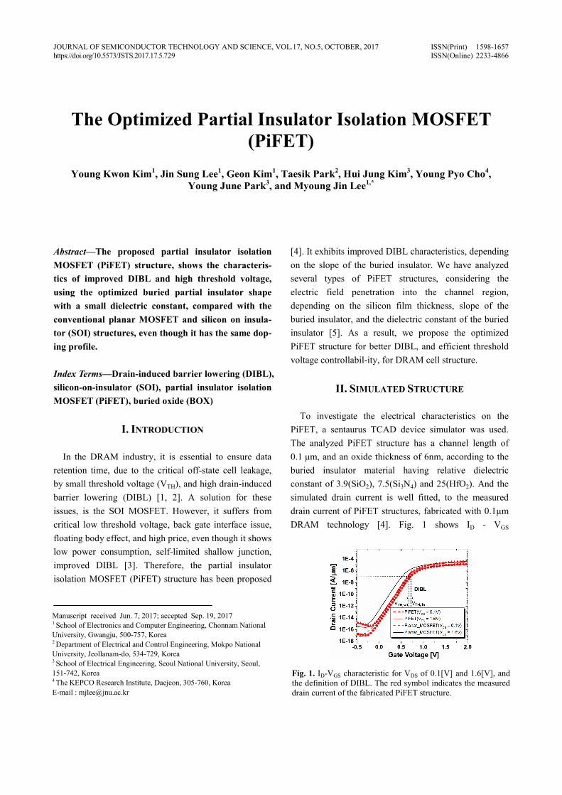
To investigate the electrical characteristics on the PiFET, a sentaurus TCAD device simulator was used. The analyzed PiFET structure has a channel length of 0.1 μm, and an oxide thickness of 6nm, according to the buried insulator material having relative dielectric constant of 3.9(SiO2), 7.5(Si3N4) and 25(HfO2). And the simulated drain current is well fitted, to the measured drain current of PiFET structures, fabricated with 0.1μm DRAM technology [4]. Fig. 1 shows ID - VGS
Fig. 1. ID-VGS characteristic for VDS of 0.1[V] and 1.6[V], and the definition of DIBL. The red symbol indicates the measured drain current of the fabricated PiFET structure.
730 YOUNG KWON KIM et al : THE OPTIMIZED PARTIAL INSULATOR ISOLATION MOSFET (PIFET)
characteristics for VDS of 0.1 [V], and 1.6 [V], in the planar MOSFET and the PiFET. The threshold voltage is measured, with the constant current method (gate voltage at drain current of 10 -7 A/μm).
III. SIMULATION ANALYSIS FOR INSULATOR
ENCROACHMENT OF THE PIFET STRUCTURE
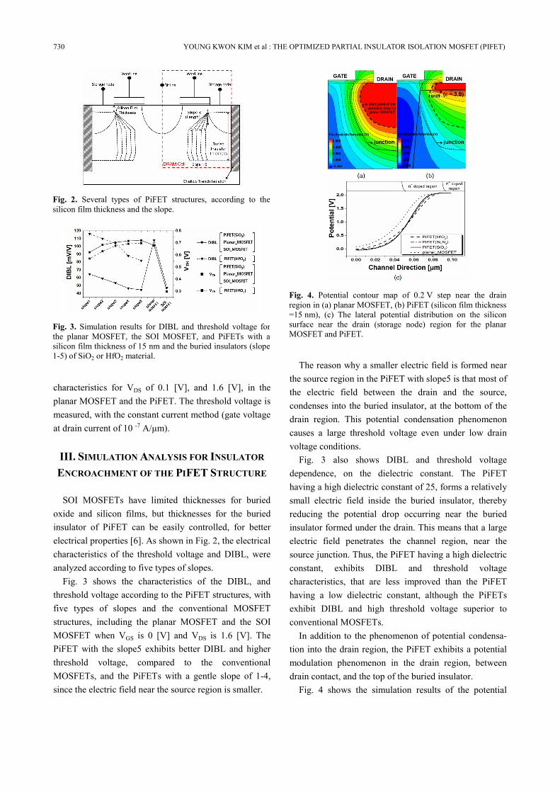
SOI MOSFETs have limited thicknesses for buried oxide and silicon films, but thicknesses for the buried insulator of PiFET can be easily controlled, for better electrical properties [6]. As shown in Fig. 2, the electrical characteristics of the threshold voltage and DIBL, were analyzed according to five types of slopes.
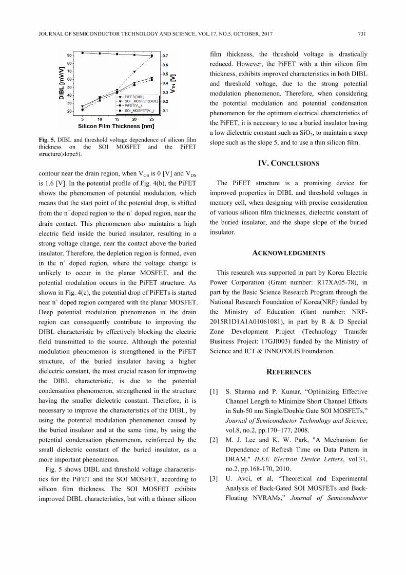
Fig. 3 shows the characteristics of the DIBL, and threshold voltage according to the PiFET structures, with five types of slopes and the conventional MOSFET structures, including the planar MOSFET and the SOI MOSFET when VGS is 0 [V] and VDS is 1.6 [V]. The PiFET with the slope5 exhibits better DIBL and higher threshold voltage, compared to the conventional MOSFETs, and the PiFETs with a gentle slope of 1-4, since the electric field near the source region is smaller.
The reason why a smaller electric field is formed near the source region in the PiFET with slope5 is that most of the electric field between the drain and the source, condenses into the buried insulator, at the bottom of the drain region. This potential condensation phenomenon causes a large threshold voltage even under low drain voltage conditions.
Fig. 3 also shows DIBL and threshold voltage dependence, on the dielectric constant. The PiFET having a high dielectric constant of 25, forms a relatively small electric field inside the buried insulator, thereby reducing the potential drop occurring near the buried insulator formed under the drain. This means that a large electric field penetrates the channel region, near the source junction. Thus, the PiFET having a high dielectric constant, exhibits DIBL and threshold voltage characteristics, that are less improved than the PiFET having a low dielectric constant, although the PiFETs exhibit DIBL and high threshold voltage superior to conventional MOSFETs.
In addition to the phenomenon of potential condensa-tion into the drain region, the PiFET exhibits a potential modulation phenomenon in the drain region, between drain contact, and the top of the buried insulator.
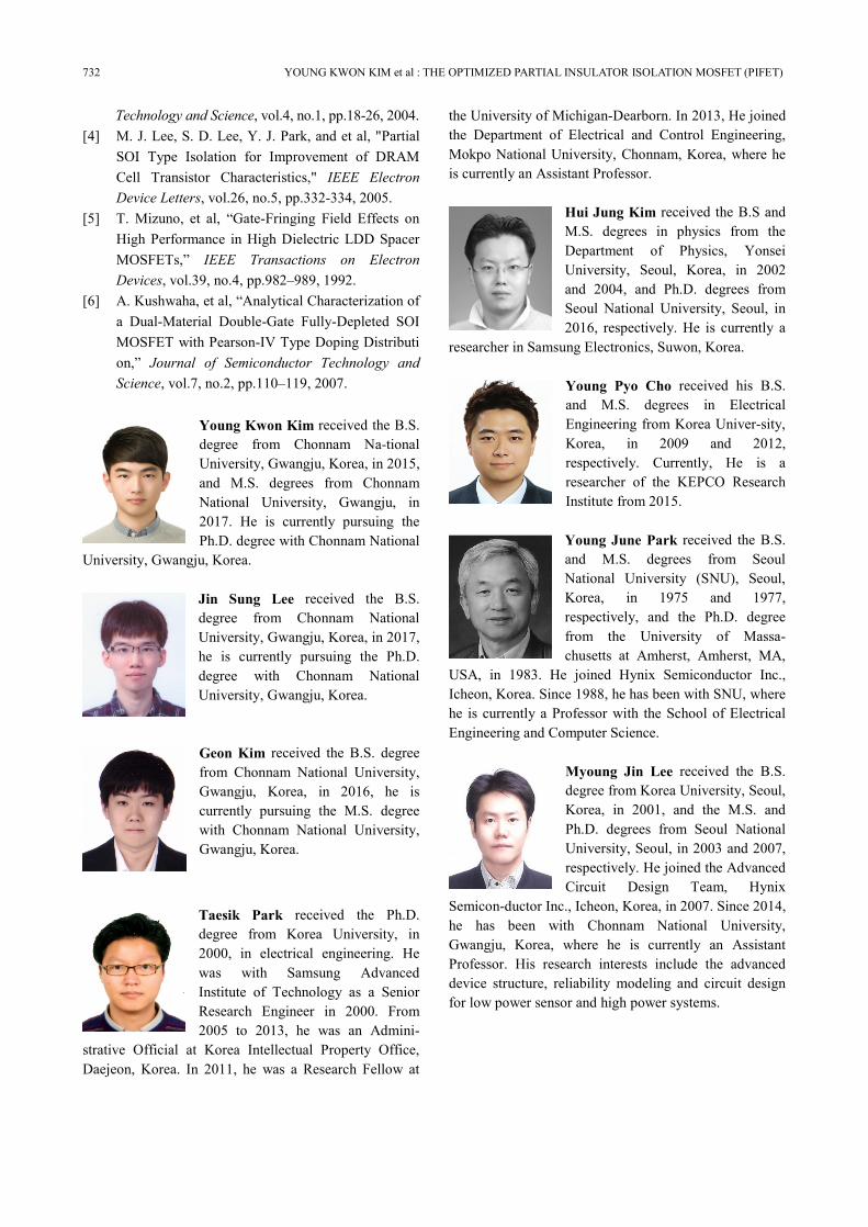
Fig. 4 shows the simulation results of the potential
Fig. 4. Potential contour map of 0.2 V step near the drain region in (a) planar MOSFET, (b) PiFET (silicon film thickness =15 nm), (c) The lateral potential distribution on the silicon surface near the drain (storage node) region for the planar MOSFET and PiFET.
Fig. 2. Several types of PiFET structures, according to the silicon film thickness and the slope.
Fig. 3. Simulation results for DIBL and threshold voltage for the planar MOSFET, the SOI MOSFET, and PiFETs with a silicon film thickness of 15 nm and the buried insulators (slope 1-5) of SiO2 or HfO2 material.
JOURNAL OF SEMICONDUCTOR TECHNOLOGY AND SCIENCE, VOL.17, NO.5, OCTOBER, 2017 731
contour near the drain region, when VGS is 0 [V] and VDS is 1.6 [V]. In the potential profile of Fig. 4(b), the PiFET shows the phenomenon of potential modulation, which means that the start point of the potential drop, is shifted from the n-doped region to the n+ doped region, near the drain contact. This phenomenon also maintains a high electric field inside the buried insulator, resulting in a strong voltage change, near the contact above the buried insulator. Therefore, the depletion region is formed, even in the n+ doped region, where the voltage change is unlikely to occur in the planar MOSFET, and the potential modulation occurs in the PiFET structure. As shown in Fig. 4(c), the potential drop of PiFETs is started near n+ doped region compared with the planar MOSFET. Deep potential modulation phenomenon in the drain region can consequently contribute to improving the DIBL characteristic by effectively blocking the electric field transmitted to the source. Although the potential modulation phenomenon is strengthened in the PiFET structure, of the buried insulator having a higher dielectric constant, the most crucial reason for improving the DIBL characteristic, is due to the potential condensation phenomenon, strengthened in the structure having the smaller dielectric constant. Therefore, it is necessary to improve the characteristics of the DIBL, by using the potential modulation phenomenon caused by the buried insulator and at the same time, by using the potential condensation phenomenon, reinforced by the small dielectric constant of the buried insulator, as a more important phenomenon.
Fig. 5 shows DIBL and threshold voltage characteris-tics for the PiFET and the SOI MOSFET, according to silicon film thickness. The SOI MOSFET exhibits improved DIBL characteristics, but with a thinner silicon
film thickness, the threshold voltage is drastically reduced. However, the PiFET with a thin silicon film thickness, exhibits improved characteristics in both DIBL and threshold voltage, due to the strong potential modulation phenomenon. Therefore, when considering the potential modulation and potential condensation phenomenon for the optimum electrical characteristics of the PiFET, it is necessary to use a buried insulator having a low dielectric constant such as SiO2, to maintain a steep slope such as the slope 5, and to use a thin silicon film.
IV. CONCLUSIONS
The PiFET structure is a promising device for improved properties in DIBL and threshold voltages in memory cell, when designing with precise consideration of various silicon film thicknesses, dielectric constant of the buried insulator, and the shape slope of the buried insulator.
ACKNOWLEDGMENTS
This research was supported in part by Korea Electric Power Corporation (Grant number: R17XA05-78), in part by the Basic Science Research Program through the National Research Foundation of Korea(NRF) funded by the Ministry of Education (Gant number: NRF-2015R1D1A1A01061081), in part by R & D Special Zone Development Project (Technology Transfer Business Project: 17GJI003) funded by the Ministry of Science and ICT & INNOPOLIS Foundation.
REFERENCES
[1] S. Sharma and P. Kumar, “Optimizing Effective Channel Length to Minimize Short Channel Effects in Sub-50 nm Single/Double Gate SOI MOSFETs,” Journal of Semiconductor Technology and Science, vol.8, no.2, pp.170–177, 2008.
[2] M. J. Lee and K. W. Park, "A Mechanism for Dependence of Refresh Time on Data Pattern in DRAM," IEEE Electron Device Letters, vol.31, no.2, pp.168-170, 2010.
[3] U. Avci, et al, “Theoretical and Experimental Analysis of Back-Gated SOI MOSFETs and Back-Floating NVRAMs,” Journal of Semiconductor
Fig. 5. DIBL and threshold voltage dependence of silicon film thickness on the SOI MOSFET and the PiFET structure(slope5).
732 YOUNG KWON KIM et al : THE OPTIMIZED PARTIAL INSULATOR ISOLATION MOSFET (PIFET)
Technology and Science, vol.4, no.1, pp.18-26, 2004. [4] M. J. Lee, S. D. Lee, Y. J. Park, and et al, "Partial
SOI Type Isolation for Improvement of DRAM Cell Transistor Characteristics," IEEE Electron Device Letters, vol.26, no.5, pp.332-334, 2005.
[5] T. Mizuno, et al, “Gate-Fringing Field Effects on High Performance in High Dielectric LDD Spacer MOSFETs,” IEEE Transactions on Electron Devices, vol.39, no.4, pp.982–989, 1992.
[6] A. Kushwaha, et al, “Analytical Characterization of a Dual-Material Double-Gate Fully-Depleted SOI MOSFET with Pearson-IV Type Doping Distributi on,” Journal of Semiconductor Technology and Science, vol.7, no.2, pp.110–119, 2007.
Young Kwon Kim received the B.S. degree from Chonnam Na-tional University, Gwangju, Korea, in 2015, and M.S. degrees from Chonnam National University, Gwangju, in 2017. He is currently pursuing the Ph.D. degree with Chonnam National
University, Gwangju, Korea.
Jin Sung Lee received the B.S. degree from Chonnam National University, Gwangju, Korea, in 2017, he is currently pursuing the Ph.D. degree with Chonnam National University, Gwangju, Korea.
Geon Kim received the B.S. degree from Chonnam National University, Gwangju, Korea, in 2016, he is currently pursuing the M.S. degree with Chonnam National University, Gwangju, Korea.
Taesik Park received the Ph.D. degree from Korea University, in 2000, in electrical engineering. He was with Samsung Advanced Institute of Technology as a Senior Research Engineer in 2000. From 2005 to 2013, he was an Admini-
strative Official at Korea Intellectual Property Office, Daejeon, Korea. In 2011, he was a Research Fellow at
the University of Michigan-Dearborn. In 2013, He joined the Department of Electrical and Control Engineering, Mokpo National University, Chonnam, Korea, where he is currently an Assistant Professor.
Hui Jung Kim received the B.S and M.S. degrees in physics from the Department of Physics, Yonsei University, Seoul, Korea, in 2002 and 2004, and Ph.D. degrees from Seoul National University, Seoul, in 2016, respectively. He is currently a
researcher in Samsung Electronics, Suwon, Korea.
Young Pyo Cho received his B.S. and M.S. degrees in Electrical Engineering from Korea Univer-sity, Korea, in 2009 and 2012, respectively. Currently, He is a researcher of the KEPCO Research Institute from 2015.
Young June Park received the B.S. and M.S. degrees from Seoul National University (SNU), Seoul, Korea, in 1975 and 1977, respectively, and the Ph.D. degree from the University of Massa-chusetts at Amherst, Amherst, MA,
USA, in 1983. He joined Hynix Semiconductor Inc., Icheon, Korea. Since 1988, he has been with SNU, where he is currently a Professor with the School of Electrical Engineering and Computer Science.
Myoung Jin Lee received the B.S. degree from Korea University, Seoul, Korea, in 2001, and the M.S. and Ph.D. degrees from Seoul National University, Seoul, in 2003 and 2007, respectively. He joined the Advanced Circuit Design Team, Hynix
Semicon-ductor Inc., Icheon, Korea, in 2007. Since 2014, he has been with Chonnam National University, Gwangju, Korea, where he is currently an Assistant Professor. His research interests include the advanced device structure, reliability modeling and circuit design for low power sensor and high power systems.