Embed Size (px)
Citation preview
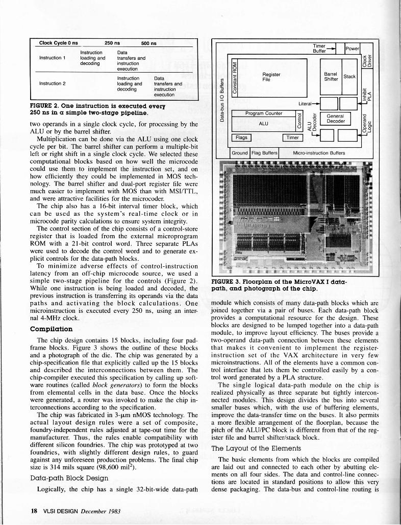
The MicroVAX I Data-path ChipGlenn Louie, Tom (Iu-meng) Ho, and Ed Cheng, Silicon Compilers, Inc., Los Gatos, CA
During 1983, Silicon Compilers, Inc. (SCI) and DigitalEquipment Corp. (DEC) implemented the MicroVAX IData-path component, which contains most of the com-putational logic of the new MicroVAX I computer manu-factured by DEC. The capabilities of the data path meetthe requirements of system designers who are currentlyusing bipolar bit-slice components such as members of theAMD 2901/29116 family. These designers can also cus-tomize microarchitectural details to fit their applications ex-actly. This full-custom nMOS chip was developed with theuse of SCI's silicon compilation tools. The developmentstrategy shows how systems companies can gain the ad-vantages of VLSI components in a timely manner.
Project Goals
The goals of the MicroVAX computer project were:
To ship the product within a yearTo make the product VAX compatible, thus offeringsignificant cost savings to DEC customersTo make the MicroVAX I computer reside on two quadboards
The team formed for this project at DEC in Bellevue,WA (DEC WEST) consisted of system designers who hadworked on the original VAX design. In developing a low-cost VAX microcomputer, DEC wanted to take advantageof VLSI technology to reduce the cost and size of theentire system. DEC also wanted the performance of theproduct to be competitive with that of the aggressive newhigh-end microprocessor-based systems that were beginningto appear on the market. Of course, the product had to becompatible with the existing VAX product line, in whichthe company and its customers had made an enormoussoftware investment. DEC's primary aim was to introducethe product quickly.
A major design goal was to implement the entire VAXon two quad-size boards (79 in 2 per board). (The originalVAX 11/780 occupied 27 hex-size boards (123 in 2 each),the VAX 11/750 required 5 extended hex-size boards (160in 2), and the VAX 11/730 required 3 hex-size boards.) Thisrequirement meant that MSI and gate-array technology,which had been used on earlier VAXs, would not providethe necessary circuit density. Furthermore, the VAX com-patibility requirement barred the use of a standardmicroprocessor.
At approximately the same time that the DEC WESTteam was beginning to investigate ways to develop the newVAX product, the management of Silicon Compilers, Inc.
decided that the company's prototype tools for full-customVLSI circuit design needed to be tested by another chipproject. (The earlier version of the silicon-compilationtools had been used to develop the first commercial Ether-netTM controller.)
Our goals were to exercise our prototype tools, and toobtain working parts within six months.
SCI's Approach to the Project
DEC's goal of shipping the product one year after incep-tion meant that a "normal" approach to custom-IC devel-opment would be impossible. There was no way SCI coulddesign a custom microprocessor chip or chip set that im-plemented the entire VAX computer, and still meet theschedule. More specifically, this project did not appear topermit the enormous development risk of any full-customVLSI project, mainly with regard to multiple design itera-tions and considerable schedule slippage.
However, we believed that we could reach all of theproject's goals by developing a single custom componentthat incorporated much of the VAX processor, but not allof it. The project began to look feasible and perhaps evenpossible. Of course, "feasible" and "possible" were rela-tive terms. "Feasible" meant that for the end product to beavailable in one year, the chip would have to be workingin nine months; the rest of the system design and produc-tion would have to be done simultaneously. All of theseelements would have to match up at the end, and workperfectly. Therefore, all component-design work wouldhave to be done in six months and would have to workright the first time. "Possible" meant that in addition tofast negotiation of a development contract and agreementon design details, nothing could be allowed to get in theway of the schedule: no surprises.
System Architecture
During the very early discussions of the system architec-ture, someone suggested that a good starting point wouldbe to implement the VAX 11/730. This machine was thesmallest VAX available at the time, and its overall sizewould need to be reduced by no more than about 56 per-cent to meet the size goal. It is always attractive to attempta size and cost reduction by re-implementing an existinginternal architecture in a new technology, instead of start-ing from scratch with a new implementation architecture.However, we soon realized just how much an implementa-tion is affected by the available technology. The VAX11/730 implementation uses 2901 bit-slice bipolar parts in
14 VLSI DESIGN December 1983
its main computational unit. This approach achieves systemperformance essentially by using fairly simple circuits run-ning very fast. MOS VLSI parts, on the other hand, aremost effective when complex circuits are run relativelyslowly. Copying the architecture of the VAX 11/730 wouldhave meant that the custom VLSI circuit had to run at a70-ns cycle time—not an attractive prospect for a part thathad to be designed very quickly and that had to bemanufacturable by several commercial foundries.
Fortunately, the VAX architecture was very well docu-mented, and SCI had access to people at DEC WEST whocould answer any question about the VAX architecture.Thus, we could proceed knowing what the final design hadto do, what was feasible in MOS ., and what the SCI toolset could do. Most important, we did not have to deducethe requirements by disassembling logic diagrams. Had thisnot been the case, we would have had little choice but totry to re-implement the same logic in the latest technology.(We already knew that the technology had not come farenough since the earlier implementation to meet the goal ofmulti-source manufacturing.)
System PartitioningOnce we had decided to implement a new internal archi-
tecture, we also had to decide which portions of it couldbest be placed on a single chip. This trade-off had to con-sider DEC's constraint of a two-board system. The com-putation engine of a computer is sometimes called the datapath, because it provides a thoroughfare for informationtransfers between the data-processing elements in the com-puter (e.g., it performs register-transfer operations). Data-processing elements include arithmetic logic units (ALUs),shifters, registers, latches, and counters. When a computercontains many data-processing elements, it is most efficientto connect these elements through common buses.Therefore, data paths are usually formed by buses andother common lines. The elements communicate with eachother not only for direct data transfer, but also while per-forming various micro-operations. The communicating ele-ments are controlled by a set of digital signals, whichusually come in from outside the data-path block. We se-lected a straightforward two-bus data-path structure for thecentral processor, and designed the memory-managementsystem as a separate logical unit operating in parallel.
The key question then became, "What parts go on thechip?" Random logic is often the first choice for integra-tion of CPUs and controllers. However, in our case, theamount of random logic was reduced by the regularstructure of the architecture, and could be implementedreadily with microcode, programmable array logic, andprogrammable logic arrays (PLAs). The data path itself ac-counted for much of the chip count in MSI. The datapath's regular design and stable functional specificationmade it the ideal candidate for quick implementation usingSCI's block compiler. Thus, we selected the data-path sec-tion of the processor and its control logic for integration onthe custom VLSI chip.
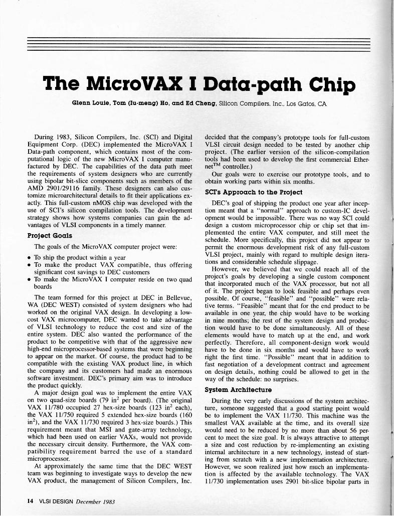
As shown in Figure I, the control store, which containsthe microprograms that implement the VAX instruction set,was not integrated onto the chip. Our decision to leave this
ROM or EPROMMicrocodeStore
Control-storeSequencer
21-bitmicro-codeword
MicroVAXData-pathChip
32-bit-wide data bus
FIGURE 1. MicroVAX system partitioning.
section outside the chip, for implementation with ROMs,was based on the following considerations:
• Incorporating the large control store on the chip wouldhave made the chip prohibitively large.
• The use of standard off-the-shelf EPROMs and ROMsstill offered the advantages of high-density VLSItechnology.
• The VAX design team at DEC WEST would be solelyresponsible for coding the VAX instruction set. Thisway, they could work on the microcode while the SCIteam worked on the chip design.
• Any late changes in the microcode (e.g. to fix bugs)could be done easily with EPROMs even after the cus-tom chip was completed; such changes would not entaillong delays for reworking the IC masks.
We also left the control-store sequencer off the chip,primarily because of the pin limitations of the package. Pinli mitations also greatly affected the design of the sys-tem/chip interface. We selected a 68-lead pin-grid arraypackage because it gave a generous number of pins in acost-effective package. We also used a single bidirectional32-bit data bus, along with a separate 21-bit control bus.These two buses alone required 53 of the pins, without in-cluding power and ground.
Microarchitecture
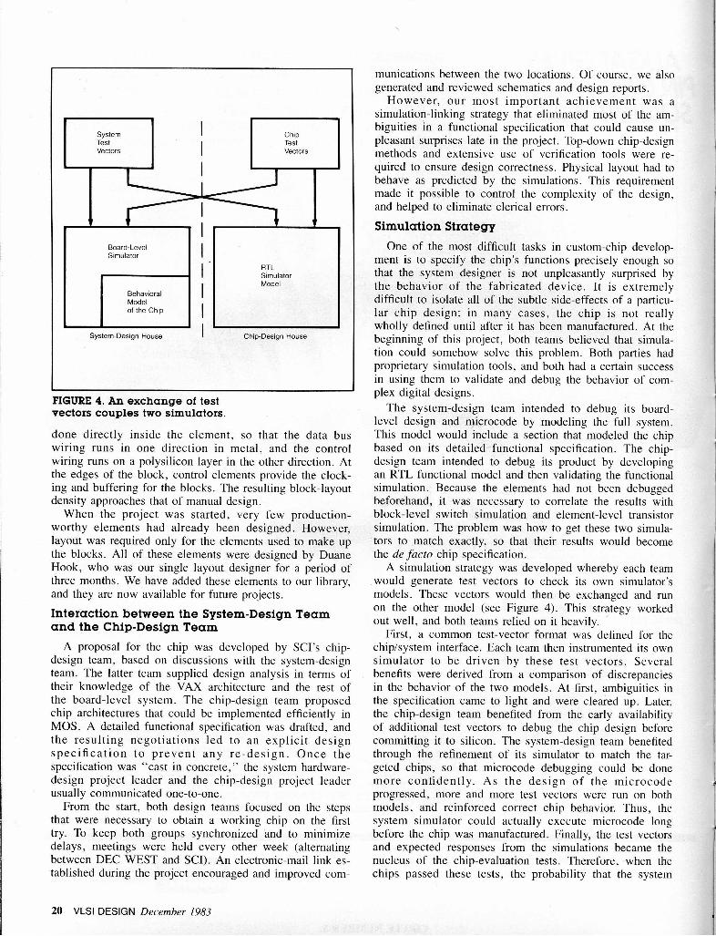
Data is processed by 32-bit-wide data-path blocks con-nected via a pair of 32-bit buses. These data-path blocksprovide the register storage and computational hardware forthe data-processing part of the system. The data path con-sists of the following blocks:
• A 47-register dual-port RAM file to hold 8-, 16-, and32-bit operands
• A 32-bit full-function ALU• A 64-bit-wide barrel shifter• A 32-bit program counter• A 7-level operand-restore stack• A 32-word constant ROM
The two buses and the dual-port RAM allow access to
VLSI DESIGN December 1983 15
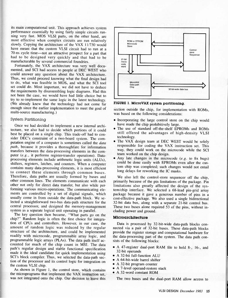
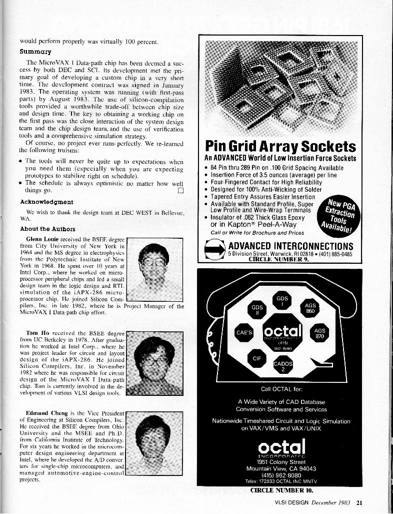
System ChipTest TestVectors Vectors
Board-LevelSimulator
RTLSimulatorModel
BehavioralModelof the Chip
System-Design House Chip-Design House
FIGURE 4. An exchange of testvectors couples two simulators.
done directly inside the element, so that the data buswiring runs in one direction in metal, and the controlwiring runs on a polysilicon layer in the other direction. Atthe edges of the block, control elements provide the clock-ing and buffering for the blocks. The resulting block-layoutdensity approaches that of manual design.
When the project was started, very few production-worthy elements had already been designed. However,layout was required only for the elements used to make upthe blocks. All of these elements were designed by DuaneHook, who was our single layout designer for a period ofthree months. We have added these elements to our library,and they are now available for future projects.
Interaction between the System-Design Teamand the Chip-Design Team
A proposal for the chip was developed by SCI's chip-design team, based on discussions with the system-designteam. The latter team supplied design analysis in terms oftheir knowledge of the VAX architecture and the rest ofthe board-level system. The chip-design team proposedchip architectures that could be implemented efficiently inMOS. A detailed functional specification was drafted, andthe resulting negotiations led to an explicit designspecification to prevent any re-design. Once thespecification was "cast in concrete," the system hardware-design project leader and the chip-design project leaderusually communicated one-to-one.
From the start, both design teams focused on the stepsthat were necessary to obtain a working chip on the firsttry. To keep both groups synchronized and to minimizedelays, meetings were held every other week (alternatingbetween DEC WEST and SCI). An electronic-mail link es-tablished during the project encouraged and improved com-
munications between the two locations. Of course, we alsogenerated andreviewed schematics and design reports.
However, our most important achievement was asimulation-linking strategy that eliminated most of the am-biguities in a functional specification that could cause un-pleasant surprises late in the project. Top-down chip-designmethods and extensive use of verification tools were re-quired to ensure design correctness. Physical layout had tobehave as predicted by the simulations. This requirementmade it possible to control the complexity of the design,and helped to eliminate clerical errors.
Simulation Strategy
One of the most difficult tasks in custom-chip develop-ment is to specify the chip's functions precisely enough sothat the system designer is not unpleasantly surprised bythe behavior of the fabricated device. It is extremelydifficult to isolate all of the subtle side-effects of a particu-lar chip design; in many cases, the chip is not reallywholly defined until after it has been manufactured. At thebeginning of this project, both teams believed that simula-tion could somehow solve this problem. Both parties hadproprietary simulation tools, and both had a certain successin using them to validate and debug the behavior of com-plex digital designs.
The system-design team intended to debug its board-level design and microcode by modeling the full system.This model would include a section that modeled the chipbased on its detailed functional specification. The chip-design team intended to debug its product by developingan RTL functional model and then validating the functionalsimulation. Because the elements had not been debuggedbeforehand, it was necessary to correlate the results withblock-level switch simulation and element-level transistorsimulation. The problem was how to get these two simula-tors to match exactly, so that their results would becomethe de facto chip specification.
A simulation strategy was developed whereby each teamwould generate test vectors to check its own simulator'smodels. These vectors would then be exchanged and runon the other model (see Figure 4). This strategy workedout well, and both teams relied on it heavily.
First, a common test-vector format was defined for thechip/system interface. Each team then instrumented its ownsimulator to be driven by these test vectors. Severalbenefits were derived from a comparison of discrepanciesin the behavior of the two models. At first, ambiguities inthe specification came to light and were cleared up. Later,the chip-design team benefited from the early availabilityof additional test vectors to debug the chip design beforecommitting it to silicon. The system-design team benefitedthrough the refinement of its simulator to match the tar-geted chips, so that microcode debugging could be donemore confidently. As the design of the microcodeprogressed, more and more test vectors were run on bothmodels, and reinforced correct chip behavior. Thus, thesystem simulator could actually execute microcode longbefore the chip was manufactured. Finally, the test vectorsand expected responses from the simulations became thenucleus of the chip-evaluation tests. Therefore, when thechips passed these tests, the probability that the system
20 VLSI DESIGN December 1983
would perform properly was virtually 100 percent.
Summary
The MicroVAX I Data-path chip has been deemed a suc-cess by both DEC and SCI. Its development met the pri-mary goal of developing a custom chip in a very shorttime. The development contract was signed in January1983. The operating system was running (with first passparts) by August 1983. The use of silicon-compilationtools provided a worthwhile trade-off between chip sizeand design time. The key to obtaining a working chip onthe first pass was the close interaction of the system design
team and the chip design team, and the use of verificationtools and a comprehensive simulation strategy.
Of course, no project ever runs• perfectly. We re-learnedthe following truisms:
• The tools will never be quite up to expectations whenyou need them (especially when you are expectingprototypes to stabilize right on schedule).
• The schedule is always optimistic no matter how wellthings go. - q
Acknowledgment
We wish to thank the design team at DEC WEST in Bellevue,WA.
About the Authors
Glenn Louie received the BSEE degreefrom City University of New York in1964 and the MS degree in electrophysicsfrom the Polytechnic Institute of NewYork in 1968. He spent over 10 years atIntel Corp.. where he worked on micro-processor peripheral chips and led a smalldesign team in the logic design and RTLsimulation of the iAPX-286 micro-processor chip. He joined Silicon Com-pilers, Inc. in late 1982, where he is Project Manager of theMicroVAX I Data-path chip effort.
Tom Ho received the BSEE degreefrom UC Berkeley in 1978. After gradua-tion he worked at Intel Corp., where hewas project leader for circuit and layoutdesign of the iAPX-286. He joinedSilicon Compilers, Inc. in November1982 where he was responsible for circuitdesign of the MicroVAX I Data-pathchip. Tom is currently involved in the de-velopment of various VLSI design tools.
Edmund Cheng is the Vice Presidentof Engineering at Silicon Compilers, Inc.He received the BSEE degree from OhioUniversity and the MSEE and Ph.D.from California Institute of Technology.For six years he worked in the microcom-puter design engineering department atIntel, where he developed the A/D conver-ters for single-chip microcomputers, andmanaged automotive-engine-controlprojects.
Pin Grid Array SocketsAn ADVANCED World of Low Insertion Force Sockets• 64 Pin thru 289 Pin on .100 Grid Spacing Available• Insertion Force of 3.5 ounces (average) per line• Four-Fingered Contact for High Reliability• Designed for 100% Anti-Wicking of Solder• Tapered Entry Assures Easier Insertion• Available with Standard Profile, Super
Low Profile and Wire-Wrap Terminals• Insulator of .062 Thick Glass Epoxy , ,
or in Kapton ® Peel-A-WayCall or Write for Brochure and Prices
ADVANCED INTERCONNECTIONS5 Division Street, Warwick, RI 02818 • (401) 885-0485
CIRCLE NUMBER 9.
CIRCLE NUMBER 10.
VLSI DESIGN December 1983 21


![Βίντεο για εκμάθηση Scratch 1€¦ · Φύλλα εργασίας για εκμάθηση Scratch 1͙4 – Κοκκόρη Αθηνά [3] Εφαρογή σο Scratch:](https://img.pdfslide.us/doc/110x75/5fa1e23ac073f719dc091d73/-f-scratch-1-f-.jpg)