Embed Size (px)
Citation preview

THE MICROIONIZER – A SOLID STATE ION SOURCE FOR
HIGH PRESSURE MASS SPECTROMETRY
Craig A. Cavanaugh
A dissertation submitted to the faculty at the University of North Carolina at Chapel Hill
in partial fulfillment of the requirements of Doctor of Philosophy in the Department of
Applied Physical Sciences.
Chapel Hill
2016
Approved by:
J. Michael Ramsey
Michael R. Falvo
Gary L. Glish
Scott C. Warren
Sean Washburn

ii
© 2016
Craig A. Cavanaugh
ALL RIGHTS RESERVED

iii
ABSTRACT
Craig A. Cavanaugh: The Microionizer – A Solid State Ion Source for
High Pressure Mass Spectrometry
(Under the direction of J. Michael Ramsey)
This work describes the development of a novel, microfabricated solid-state ionization
source (a “microionizer”) for use with high pressure mass spectrometry (HPMS). HPMS is
intended for miniature, low-cost, portable instrumentation. As such, the microionizer is
designed as a small, low-power ion source compatible with the 1 Torr air-based environment
of HPMS. The microionizer is a field effect device based upon silicon-on-insulator
technology that functions as a dual-source, producing field emission for internal electron
impact ionization (EI) and external field ionization.
External ion injection into the miniature cylindrical ion trap (mCIT) was performed in
helium, nitrogen, or air buffer gases at 1 Torr using traditional ion sources (thermionic
emitter and glow discharge) for proof-of-concept experiments. Further studies in helium and
air examined the effects of pressure, ion kinetic energy, and ion trap potential well depth
changes with drive radiofrequency (RF) signal frequency and amplitude. Results indicated
that mass spectral signal intensity can be maximized at pressures ranging from 10 to
1000 mTorr by tuning ion kinetic energy between 20 to 250 eV and increasing potential well
depth aids external ion injection.
Nine generations of microionizers were fabricated to optimize microionizer performance.
The first generation microionizer was coupled with HPMS as a field emission source and
generated helium and air-based high pressure mass spectra. However, high current draw

iv
limited the microionizer lifetime and prevented field strengths necessary for field ionization.
Generations two through nine encompassed processing variations of device fabrication
procedures, development of robust electrical contacts, and microionizer device incorporation
into the ion trap electrode stack, leading to improved microionizer signal intensity and low
power (< 1 mW average power) consumption.
The ninth generation microionizer demonstrated operation as both a field emission and
field ionization source in air buffer gas at 1 Torr. Electric field strengths for field emission
were near 1 MV/cm, while field ionization required greater than 1.8 MV/cm. The
microionizer generated mass spectra of volatile organic compounds (such as benzene and
dimethylaniline) in both modes and lifetime was found to be 9 h for field emission and 490 h
for field ionization under continuous mass spectral acquisition.

v
To my family

vi
ACKNOWLEDGEMENTS
First, I thank my advisor, J. Michael Ramsey, for the opportunity to work in his research
group; the knowledge, skills, and experience gained here are unique and will prove to be
invaluable in future endeavors. Thank you to all the members of the Ramsey group for the
past five and half years for helping to make the group what it is, particularly the Mini-Mass
Spec subgroup for constantly challenging ideas and supporting experimental progress,
particularly Derek Wolfe, Kenion Blakeman, Mac Gilliland, Andrew Hampton, and Kevin
Schultze. Thank you to Rob Musser, you always have a practical solution to problems and
were crucial in hardware design and repair. Thank you to Tina Stacy, J. P. Alarie, Hamp
Henley, and John Perry for practical and professional guidance as well as mentoring. I also
thank everyone in the Chapel Hill Analytical and Nanofabrication Laboratory (CHANL) -
Carrie Donley, Bob Geil, Amar Kumbhar, and Wallace Ambrose – for your patience in
teaching the fundamentals of surface characterization and microfabrication. I thank Ed
Samulski for giving me a chance when I first moved to North Carolina and encouraging me
to return to school for my doctorate. Finally, I thank my family (near and far). Without your
boundless support, I would never have finished.

vii
TABLE OF CONTENTS
LIST OF TABLES .................................................................................................................. xii
LIST OF FIGURES ............................................................................................................... xiii
LIST OF ABBREVIATIONS AND SYMBOLS ................................................................ xviii
CHAPTER 1: INTRODUCTION – HIGH PRESSURE MASS SPECTROMETRY
AND THE MICROIONIZER ............................................................................................. 1
1.1 Motivation for Handheld Mass Spectrometry........................................................... 1
1.2 Current Technology in Miniaturized Mass Spectrometers ....................................... 3
1.2.1 Miniaturized Mass Analyzers ............................................................................ 4
1.2.2 Portable Ion Trap Mass Spectrometers .............................................................. 4
1.3 High Pressure Mass Analysis.................................................................................... 7
1.3.1 System Components for HPMS – Mass Analyzer ............................................. 9
1.3.2 System Components for HPMS – Ion Detector ............................................... 11
1.3.3 System Components for HPMS – Ion Source.................................................. 12
1.4 Advanced Ion Sources ............................................................................................ 13
1.4.1 Internal vs. External Ionization ........................................................................ 15
1.4.2 Ionization Methods for High Volatility Analytes ............................................ 16
1.4.3 Field Effect Devices for Mass Spectrometry ................................................... 18
1.5 Field Effect Applications and Theory ..................................................................... 20
1.5.1 Field Emission ................................................................................................. 20
1.5.2 Field Ionization ................................................................................................ 23

viii
1.5.3 Pressure Tolerance and Lifetime ..................................................................... 24
1.5.4 Fabrication ....................................................................................................... 25
1.6 Solid State Microionizer ......................................................................................... 26
1.6.1 Design and Operation ...................................................................................... 26
1.6.2 Examples of Similar FEDs............................................................................... 28
1.6.3 Advantages of the Microionizer....................................................................... 29
1.7 Objectives and Roadmap ........................................................................................ 30
1.8 Figures..................................................................................................................... 31
1.9 REFERENCES ....................................................................................................... 37
CHAPTER 2: THERMIONIC AND GLOW DISCHARGE SOURCES
FOR HPMS APPLICATIONS ......................................................................................... 53
2.1 Introduction ............................................................................................................. 53
2.2 Experimental Section .............................................................................................. 55
2.3 Results and Discussion ........................................................................................... 59
2.4 Conclusions ............................................................................................................. 68
2.5 Figures..................................................................................................................... 70
2.6 REFERENCES ........................................................ Error! Bookmark not defined.
CHAPTER 3: INITIAL MICROIONIZER DEVELOPMENT .............................................. 83
3.1 Introduction ............................................................................................................. 83
3.2 Experimental ........................................................................................................... 87
3.3 Results and Discussion ........................................................................................... 88
3.3.1 1st Generation Microionizer as a Field Emission Source ................................ 89
3.3.2 Mass Spectrometry in Helium Buffer Gas ....................................................... 91

ix
3.3.3 Mass Spectrometry in Air Buffer Gas ............................................................. 92
3.3.4 1st Generation Microionizer Characterization .................................................. 93
3.4 Conclusions ............................................................................................................. 95
3.5 Figures..................................................................................................................... 97
3.6 REFERENCES ........................................................ Error! Bookmark not defined.
CHAPTER 4: MICROIONIZER FABRICATION AND DEVELOPMENT ...................... 110
4.1 Introduction ........................................................................................................... 110
4.2 Fabrication ............................................................................................................ 113
4.2.1 Early Development – Generations 2 to 6 ....................................................... 115
4.2.2 Optimization – Generations 7 through 8 ........................................................ 116
4.2.3 Final Process – Generation 9 ......................................................................... 116
4.3 Experimental ......................................................................................................... 117
4.3.1 HPMS Updates............................................................................................... 117
4.3.2 Microionizer Operation .................................................................................. 118
4.3.3 Characterization and Testing ......................................................................... 120
4.4 Results and Discussion ......................................................................................... 121
4.4.1 Fabrication and Leakage Current ................................................................... 121
4.4.2 Field Emission Mode Operation .................................................................... 126
4.4.3 Positive Mode Operation ............................................................................... 130
4.5 Conclusions ........................................................................................................... 132
4.6 Figures................................................................................................................... 134
4.7 REFERENCES ........................................................ Error! Bookmark not defined.
CHAPTER 5: MICROIONIZER-BASED HIGH PRESSURE
MASS SPECTROMETRY ............................................................................................. 157

x
5.1 Introduction ........................................................................................................... 157
5.2 Experimental ......................................................................................................... 159
5.3 Results and Discussion ......................................................................................... 162
5.3.1 Field Emission HPMS Characterization ........................................................ 162
5.3.2 Field Ionization HPMS Characterization ....................................................... 166
5.3.3 Modes of Failure ............................................................................................ 174
5.4 Conclusions ........................................................................................................... 175
5.5 Figures................................................................................................................... 176
5.6 REFERENCES ........................................................ Error! Bookmark not defined.
CHAPTER 6: CONCLUSIONS AND FUTURE WORK .................................................... 189
6.1 Conclusions ........................................................................................................... 189
6.2 Future Work .......................................................................................................... 192
6.2.1 Microionizer as Atmospheric Inlet ................................................................ 193
6.2.2 Microionizer as Ion Trap Endcap .................................................................. 194
6.2.3 Further Microionizer Development ............................................................... 195
6.3 Applications Beyond HPMS ................................................................................. 196
6.4 Figures................................................................................................................... 197
6.5 REFERENCES ........................................................ Error! Bookmark not defined.
APPENDIX 1: LIST OF MICROFABRICATION TECHNIQUES,
TOOLS, AND GENERAL RESOURCES ..................................................................... 201
A1.1 Tools and Techniques Used During Fabrication Development ......................... 201
A1.2 Notes and Resources .......................................................................................... 202
A1.2.1 General Resources....................................................................................... 202

xi
A1.2.2 Cleaning and Wet Etches ............................................................................ 202
A1.2.3 AZ-9260 Guidelines .................................................................................... 204
A1.2.4 Thin Metallic Films ..................................................................................... 205
A1.2.5 Dry Etching ................................................................................................. 206
A1.3 REFERENCES...................................................... Error! Bookmark not defined.
xii
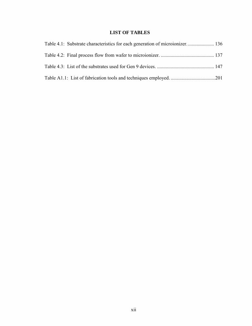
LIST OF TABLES
Table 4.1: Substrate characteristics for each generation of microionizer. ..................... 136
Table 4.2: Final process flow from wafer to microionizer. ........................................... 137
Table 4.3: List of the substrates used for Gen 9 devices. .............................................. 147
Table A1.1: List of fabrication tools and techniques employed. ....................................201

xiii
LIST OF FIGURES
Figure 1.1: Cross sectional schematics of quadrupole and cylindrical
ion traps showing critical dimensions and equipotential lines...................................31
Figure 1.2: Stability diagram for a quadrupole ion trap, where mass
selective instability mode is highlighted in red..........................................................32
Figure 1.3: Examples of conventional ionization sources including a
thermionic emitter as well as glow discharge. ...........................................................33
Figure 1.4: Examples of field effect devices which have been coupled
with mass spectrometers. ...........................................................................................34
Figure 1.5: A cross-sectional schematic of the microionizer including
the high-field region, operational voltages, and layering of the
SOI substrate. .............................................................................................................35
Figure 1.6: First generation microionizer layout with an SEM magnification
of an array of active features as well as a single 20 µm via. .....................................36
Figure 2.1: a) An exploded rendering of the differentially pumped
mass spectrometer (HPMS). ......................................................................................70
Figure 2.2: a) Schematics of external ion sources including the off-axis
electron impact ionization source and on-axis glow discharge source. .....................71
Figure 2.3: Normalized mass spectra of mesitylene generated using the
off-axis EI source in helium and nitrogen buffer gases at 1030
and 405 mTorr, respectively. .....................................................................................72
Figure 2.4: Integrated mass spectral signal of mesitylene as a function
of pressure in helium and nitrogen buffer gases recorded using
the off-axis EI source. ................................................................................................73
Figure 2.5: Faraday plate measurement of the current density as a function
of GD bias in both ion and electron modes at 1015 mTorr in air
buffer gas. ..................................................................................................................74

xiv
Figure 2.6: Mass spectra of mesitylene in air buffer gas at 1015, 630,
and 375 mTorr taken with the on-axis ion source with energies
between 0 and 150 eV ................................................................................................75
Figure 2.7: Mesitylene mass spectra recorded at 1015 mTorr in air buffer
gas with on-axis glow discharge in both ion and electron modes. .............................76
Figure 2.8: Drive RF amplitude effects on ion injection at 1 Torr with the
mCIT using mesitylene and on-axis glow discharge. ................................................77
Figure 2.9: Drive RF frequency effects on ion injection at 1 Torr with the
mCIT using on-axis glow discharge. .........................................................................78
Figure 3.1: Optical and SEM images of the microionizer, including a cross
sectional view highlighting the layers of the SOI substrate. ......................................97
Figure 3.2: Image of the microionizer mount used at UNC as well as a
schematic of the device showing the operation voltages. ..........................................98
Figure 3.3: Summary of ORNL microionizer results for a single trench
device operated at various bias voltages of various analytes in
helium buffer gas. ......................................................................................................99
Figure 3.4: Mass spectra of xenon in helium buffer gas at 4.9 mTorr and
960 mTorr recorded with the first microionizer. .......................................................100
Figure 3.5: Mass spectrum of mesitylene in 510 mTorr of room air recorded
with the first generation microionizer. .......................................................................101
Figure 3.6: Integrated mass spectral signal intensity of xenon in helium
buffer gas as a function of microionizer electric field strength. ................................102
Figure 3.7: Integrated mass spectral signal intensity of xenon in helium
buffer gas as a function of microionizer bias potential. .............................................103
Figure 4.1: Microfabrication process flow steps used to produce the
first generation microionizer. .....................................................................................134

xv
Figure 4.2: Optical image of representative microionizers from each
generation of development. ........................................................................................135
Figure 4.3: Optical images of each version of the 9th generation microionizer
as well as a PCB-mounted and wire-bonded microionizer. .......................................138
Figure 4.4: Evolution of the HPMS, showing the decrease in mCIT size
as well as the vacuum chamber. .................................................................................139
Figure 4.5: Comparison of the output pulse voltage of the PVA 3354n
optical relay vs. the High-Voltage Switch. ................................................................140
Figure 4.6: Evolution of the microionizer PCB mount. ........................................................141
Figure 4.7: Cross-sectional SEM of Gen 9.3 device, the bias and pulse
voltages are schematically shown as well as a high-resolution
SEM of field enhancement sites. ...............................................................................142
Figure 4.8: Schematic of the microionizer test setup used to measure
field emission and ionization intensity. .....................................................................143
Figure 4.9: Representative current draws as a function of electric field
strength for three generations of microionizers: Gen 5; Gen 8; and Gen 9. .............144
Figure 4.10: Images of Gen 8 wire bonds utilizing 1 mil diameter aluminum
wire and titanium/copper bond pads and Gen 9 wire bonds consisting
of 0.5 x 1.5 mil2 gold ribbon and titanium/palladium/gold bond pads. ....................145
Figure 4.11: Image of processed Gen 9.6 wafer and summary of wafer-level
failure analysis. ..........................................................................................................146
Figure 4.12: Field emission signal intensity as a function of electric field
strength for Gen 9.1, 9.3, 9.5, and 9.6 microionizers as well as a
Fowler-Nordheim re-plot of the results. ....................................................................148
Figure 4.13: Cross sectional SEM of Gen 9.1 and Gen 9.6 highlighting a
notch in the device layer of the Gen 9.6 devices. ......................................................149

xvi
Figure 4.14: Field emission signal intensity as a function of a gating
potential at 1 Torr for a Gen 9.5 microionizer as well as average
current consumption during field emission for Gen 9.1, 9.3, 9.5,
and 9.6 microionizer. .................................................................................................150
Figure 4.15: Field ionization signal intensity as a function of electric
field strength for Gen 9.1, 9.3, 9.5, and 9.6 as well as field
ionization signal intensity versus gating potential for a Gen 9.5
microionizer. ..............................................................................................................151
Figure 5.1: Cross sectional schematic of the mini-chamber HPMS with
a trap mounted microionizer. .....................................................................................176
Figure 5.2: The mini-chamber HPMS adapted to work with the trap-mounted
microionizer. ..............................................................................................................177
Figure 5.3: High pressure mass spectrum of o-xylene at 1.0 Torr air buffer
gas using the microionizer in field emission mode. ...................................................178
Figure 5.4: The lifetime of a Gen 9.1 microionizer operated in field emission
mode in air buffer gas. ...............................................................................................179
Figure 5.5: Mass spectra of several VOCs (mesitylene; toluene; benzene;
and aniline, methylaniline, and dimethylaniline) acquired in field
ionization mode at 0.93 Torr of room air. ..................................................................180
Figure 5.6: Overlay of mesitylene mass spectra (as well as ionization pulse)
in air buffer gas with similar signal intensity recorded in field emission
and positive modes. ....................................................................................................181
Figure 5.7: Mass spectra of a dimethylaniline and benzene mixture using
field ionization with increasing field strengths of 1.17 MV/cm;
1.53 MV/cm; 1.67 MV/cm; and 1.80 MV/cm. ..........................................................182
Figure 5.8: SNR and total integrated signal of mass spectra taken in
field ionization mode with increasing concentrations of mesitylene
at a constant 1 Torr total pressure. .............................................................................183

xvii
Figure 5.9: Mesitylene mass spectral signal intensity as a function of
ion kinetic energy at 1.0 Torr and 0.5 Torr of air buffer gas. ....................................184
Figure 5.10: The lifetime of a Gen 9.1 microionizer operated in
field emission mode in air buffer gas. ........................................................................185
Figure 6.1: Schematic and image of the atmospheric inlet mini-chamber. ..........................197

xviii
LIST OF ABBREVIATIONS AND SYMBOLS
APCI atmospheric pressure chemical ionization
APGDI atmospheric pressure glow discharge ionization
ARDE aspect ratio dependent etch
ASU Arizona State University
CFE cold field emission
CHANL Chapel Hill Analytical and Nanofabrication Laboratory
CI chemical ionization
CID collision induced dissociation
CIT cylindrical ion trap
cm centimeter
CWA chemical warfare agent
CWS chemical warfare simulant
Da/s Dalton/second
DAPI discontinuous atmospheric pressure inlet
DART direct analysis in real time
DESI desorption electrospray ionization
DIMP diisopropylmethane phosphonate
DMA dimethyl aniline
DMMP dimethyl phosphonate
DRIE deep reactive ion etching
EI electron (impact) ionization
EMT electron multiplier tube

xix
ESI electrospray ionization
ETE edge-to-edge emitter
eV electron-Volt
FI field ionization
FE field emission
FEA field emission array
FED field effect device
FET field effect transistor
GC gas chromatography
GD glow discharge
GDe negative mode GD
GDi positive mode GD
HPMS high pressure mass spectrometry
IE ionization energy
ITMS ion trap mass spectrometry
L liter
LD laser desorption
LOD limit of detection
lpi lines per inch
MALDI matrix assisted laser desorption ionization
m meter
MEMS microelectromechanical systems
μL microliter

xx
mL milliliter
μm micrometer, micron
mm millimeter
mW milliwatt
MS mass spectrometry
MSn tandem mass spectrometry
m/z mass to charge ratio
ni nitride
nm nanometer
ORNL Oak Ridge National Laboratory
ox silicon dioxide
PCB printed circuit board
ppm part per million
QIT quadrupole ion trap
RIE reactive ion etching
RIT rectilinear ion trap
RF radio frequency
RVMD Rogue Valley Micro Devices, Inc
sccm standard cubic centimeter per minute
scfh standard cubic foot per hour
SEM scanning electron micrograph
SIM soft ionization membrane
SIMS secondary ion mass spectrometry

xxi
SLIT stretched length ion trap
SOI silicon-on-insulator
SC single crystal
SNR signal-to-noise ratio
SWaP size, weight, and power
TIC toxic industrial compound
TOF time of flight
UA University of Arizona
UHP ultrahigh purity
UNC University of North Carolina
V Volt
Vp pulse voltage
Vb bias/float voltage
Vpp peak-to-peak voltage
V0-p zero-to-peak voltage
VME vacuum microelectronics
VOC volatile organic compound
1
CHAPTER 1: INTRODUCTION – HIGH PRESSURE MASS SPECTROMETRY
AND THE MICROIONIZER
1.1 Motivation for Handheld Mass Spectrometry
Among analytical instrumentation, mass spectrometry (MS) offers a unique combination
of selectivity, sensitivity, and speed and is often considered the gold standard for chemical
analysis.1 On-site, rapid chemical identification is important in many fields from
environmental protection to national security with analytes of interest including: toxic
industrial compounds (TIC); volatile organic compounds (VOC); explosives; and chemical
warfare agents (CWA).2 Mass spectrometry is the ideal technique for in-field analysis,
especially when informed (and potentially costly) decisions need to be made in a timely
manner for health and safety reasons. A recent example of this occurred in 2014 when
Freedom Industries spilled 10,000 gal of methylcyclohexane-methanol into the Elk River in
West Virginia.3 The Kanawha Valley water treatment plant attempted to process the
unknown, excess organics that suddenly appeared at the upstream side of the plant.
However, the carbon filtration system was quickly overwhelmed and a ‘Do Not Use’ order
was issued until these could be regenerated, leaving 300,000 residents without tap water for
weeks.4 Had the operators at the treatment plant access to a rapid, detailed chemical analysis,
quicker, informed decisions could have been made potentially avoiding the extended
downtime. Mass spectrometry would have been ideal for this situation; however, it is
typically confined to the laboratory because of size (kitchen refrigerator), weight (hundreds
of pounds), and power (kilowatts) as well as cost considerations.

2
Miniature mass spectrometers have been investigated for decades; the first suitcase-sized,
field portable mass spectrometer was disclosed in 19955 and currently, there are several
commercial systems available.6 Moreover, there is a demonstrated need for in-field mass
analysis.7 Despite availability and demand, mass spectrometry has yet to become ubiquitous
in the field because of size, cost, lack of robustness, and operator skill required. Many of the
field portable systems on the market share an important trait with their lab-sized counterparts
– cost both in capital (> $100k) and trained personnel to operate the instrument and interpret
data.
The Ramsey group at the University of North Carolina at Chapel Hill has focused on
bridging the divide – attempting to move mass spectrometry out of the laboratory and into
the field in a cost-friendly manner. The primary method for accomplishing this is to operate
the mass spectrometer at pressures negating the need for the most expensive, highest power-
consuming component, the turbomolecular pump. This pump elimination requires operation
at pressures greater than 100 mTorr. In comparison, traditional mass spectrometry requires
≤ 1 mTorr vacuum conditions and uses a two-stage pumping system, typically roughing +
turbo pumps. Operating the mass spectrometer at pressures ≥ 100 mTorr is referred to as
high pressure mass spectrometry (HPMS), which can be accomplished using simple
miniature-roughing pump with reasonable flow rates and continuous, atmospheric sampling.
Operating under HPMS conditions and atmospheric sampling requires that the three
major subsystems of the mass spectrometer (mass analyzer, ion detector, and ion source) be
compatible with a vacuum environment composed of ambient air. Because portability is a
key goal, these subsystems should each have small footprints and low-power consumption.
The work presented in this dissertation focuses on one subsystem – the ion source. The main

3
objective was the development of a silicon-based solid state, field effect ionization source or
microionizer. Incorporating the microionizer within the HPMS system requires an
understanding of internal and external ion trapping under HPMS conditions, which was
performed with currently available MS ionization sources. HPMS with the microionizer
additionally required developing silicon microfabrication procedures; general instrument
design and construction; ion trap mass spectrometry (ITMS); and finally generating ions and
characterizing performance.
This chapter introduces the background necessary to understand the need for a low
power, field effect microionizer as well as the principle of operation behind the device.
Section 1.2 begins with a survey of current, miniaturized mass spectrometers. Section 1.3
highlights important theoretical details for HPMS as well as the current state of system
components used in HPMS research. Section 1.4 covers traditional ion sources that have
been coupled with mass spectrometry, including field effect devices; providing context for
the microionizer. Section 1.5 introduces field effect theory and highlights the progression of
field emission and field ionization devices. The microionizer is formally introduced in
Section 1.6. Finally, Section 1.7 provides an outline of the objectives for this dissertation.
1.2 Current Technology in Miniaturized Mass Spectrometers
Miniaturization of a mass spectrometer balances the needs of the intended application
(instrument performance) with the requirements for portability (size, weight, and power,
SWaP).6 This performance-portability trade-off covers a broad spectrum. On one end, when
resolving power is paramount then portability is sacrificed as seen with the refrigerator-sized,
miniature Fourier transform ion cyclotron resonance mass spectrometer (FT-ICR).8 On the
other end, where portability is key, instrument performance is tuned to the lowest possible

4
necessary to accomplish the task, such as the palm portable mass spectrometer which
samples at 0.02 Hz.9 The focus of HPMS is to raise instrument performance on the
portability end of the spectrum where SWaP is a premium. HPMS does this not only by
miniaturizing the hardware but also by adapting mass analysis in the high pressure regime (1
Torr vs. 1 mTorr).6, 10
To better understand the HPMS approach, a brief survey of
miniaturized mass analyzers is useful.
1.2.1 Miniaturized Mass Analyzers
Nearly every form of mass analyzer has been miniaturized8 and includes time of flight
(ToF);11
electric and magnetic sectors;12
linear quadrupole;13-14
and three-dimensional ion
traps.15-17
ToF and sector-based analyzers use static (or field-free) regions and require high
vacuum (less than 10-6
Torr) to maintain mass to charge ratio (m/z) separation. Linear
quadrupoles use both static DC and dynamic RF voltages to generate electric fields where a
single m/z is contained in two-dimensions and travels along the third to the detector. Since
ions are actively guided, linear quadrupoles can operate at higher pressures than TOF and
sectors; up to 0.01 Torr for highly miniaturized analyzers.18
Three-dimensional ion traps use
RF voltages to maintain a stable trapping volume at the center of the trap. Ion traps naturally
operate at high pressure (10-3
Torr) because the ion trajectory is completely defined by the
electric field, thus performance is less susceptible to ion-neutral scattering than the
previously mentioned mass analyzers.19
This has lead them to be the mass analyzer of choice
for the majority of miniaturized MS with portability as the key design factor.
1.2.2 Portable Ion Trap Mass Spectrometers
The pressure tolerance of three-dimensional ion traps is ideal for portable applications
because the vacuum systems can be reduced in size, power, and complexity. In addition to

5
pressure tolerance, ion traps have two more desirable properties: mass resolution is
independent of trap size20
and the ability to perform tandem mass spectrometry (MSn).
21-22
As such, considerable efforts have been placed into miniaturizing quadrupole ion traps
(QIT).23
One issue with the QIT is that it uses hyperbolic electrodes that become difficult to
fabricate at smaller scales (radius < 1 cm),24
which translates into higher costs for the mass
analyzer. An example is the toroidal ion trap, which has a large charge capacity (and hence
improved sensitivity) relative to a standard QIT, but is more difficult to fabricate.25
Geometric variants have been developed to overcome this issue including the rectilinear ion
trap (RIT)26
and the cylindrical ion trap (CIT).27
Each variant has been incorporated into a
miniature mass spectrometer such as: Guardion GC-MS (Smith Detection, Inc) based upon
the toroidal ion trap;28
the Mini-series of instruments from Purdue based upon the RIT;29-30
and the MMS-1000 (1st Detect, Inc) based upon the CIT.
31-32 The Guardion GC-MS is a
ruggedized, briefcase-sized system which weighs > 30 lb and has less than 8 h battery life,
while the MMS-1000 is a small, lightweight benchtop system designed to be used with wall
power, thus it is best for stationary settings such as airport security checkpoints. The Mini-
series has variants covering the spectrum from hand-portable26
to benchtop.30
The Mini-instruments offer an interesting view into the miniaturization of the remaining
subsystems of the mass spectrometer: the vacuum system, ion detector, and ion source. The
vacuum system required is defined by the choice of mass analyzer and detector. The
resolution of the RIT is best at lower pressures (< 10 mTorr),33
which requires the use of a
turbo pump. Miniature turbo pumps have been developed specifically for portable MS use,
but they are specialized, expensive, and fragile.34-35
Despite miniaturization, these pumps
still consume a significant portion of the power and space budget of the instrument.36
While

6
the inclusion of a turbo pump increases SWaP, the low pressure enables the use of electron
multiplier tubes (EMT) or microchannel plates (MCP) for ion detection. Because these
devices have high sensitivity and bandwidth,37
there has yet to be a significant emphasis on
incorporating alternative (pressure tolerant) ion detectors.26, 30
Ion sources are a different matter because each source has strengths and weaknesses for
particular applications. Most miniature mass spectrometers are geared towards detecting
gaseous analytes, thus electron impact ionization (EI) is a staple and can be achieved via
thermionic emitters26
or plasma generators.29
Lower volatility analytes require ambient
ionization techniques and the Mini-instruments have been adapted for several methods
including low temperature plasma (LTP)35
and desorption electrospray ionization (DESI).38
However, each of these techniques requires sampling at atmospheric pressure, which strains
the vacuum system. The discontinuous atmospheric pressure interface (DAPI) was
introduced to counteract the increased power consumption caused by a constant gas load on a
turbo pump.39
In DAPI, an inlet is opened and a high gas load is imposed for sampling. The
inlet is then closed and a pump-down time is added to achieve < 10 mTorr operating range
for the RIT and EMT. Low pressure during mass analysis improves resolution and the
discontinuous gas flow improves battery life. However, DAPI limits data acquisition to
about 1 Hz as well as the maximum RF trapping voltage amplitude during ionization. This is
an example of a trade-off made to bridge the gap between person-portable and hand-
portability when a turbo pump is required for operation.6
The palm-portable mass spectrometer (PPMS) is an extreme example of DAPI. Similar
to other fieldable systems it uses a low pressure ITMS, but maintains pressure with a
miniature two-stage vacuum system (roughing + getter pump).9 Baseline pressure (≈

7
10-6
Torr) is achieved with a standard benchtop pumping system, then the PPMS is taken into
the field for use. The maximum sample rate is only 0.2 Hz. However, this rate exhausts the
getter’s limited capacity in under an hour. In order to achieve day-long operation, the
sampling rate is further reduced to just 0.02 Hz (≈ 1 sample/minute). The acquisition rate
and small sampling volume negatively impacts sensitivity and limits the applications
available to the PPMS. However, the PPMS represents a functional departure from
dependence on high-cost, fragile turbo pumping systems.30, 35
HPMS departs even further from the miniaturization efforts of the past and has been
successfully realized in a commercial mass spectrometer. The M908, introduced in 2014 by
908 Devices, Inc. fulfills the promise of a truly handheld mass spectrometer. This system is
based upon the theory of HPMS and is licensed technology from the Ramsey group.40
The
pumping system relies upon a custom, miniature roughing pump that maintains HPMS
conditions for a CIT-based trap design and pressure tolerant ion generation and detection.
The end result is a rugged, low-cost unit coming in at just 22.5 x 18.5 x 7.6 cm3 and 2.0 kg
(including battery)41
which is already being used in the field for threat detection such as
explosives and CWAs.42
The realization of handheld mass spectrometry has guided research
efforts to improve the three major subsystems (mass analyzer, ion detector, and ion source) in
order to continue lowering the cost and expand the utility and ubiquity of HPMS.
1.3 High Pressure Mass Analysis
To successfully develop an ionization source, an understanding of how ion traps work at
higher pressures is necessary. The historical and theoretical groundwork for ion trap-based
HPMS has been thoroughly described elsewhere.43-45
Key topics regarding quadrupole ion
trap theory pertinent to ionization are highlighted here. The QIT consists of three electrically

8
insulated electrodes – two grounded endcaps and a center ring electrode. For a QIT, the
electrodes follow a hyperbolic geometry, while a CIT is a cylindrical approximation. A cross
sectional view of the QIT vs. CIT can be seen in Figure 1.1. The critical dimensions of the
trap are defined as the radius of the ring electrode, r0, and the endcap-to-trap center spacing,
z0. A radio frequency (RF) potential applied to the center ring generates a quadrupolar
electric field and ions can oscillate in stable trajectories inside the field according to axial (az
and qz) and radial (ar and qr) stability parameters. These parameters are proportional to the
DC offset of the RF waveform (an) as well as the RF voltage amplitude (qn).46
Regions of
stable ion trajectory can be viewed using a stability diagram, shown by plotting the axial
stability parameters, az vs. qz.47
The stability diagram for a QIT is plotted in Figure 1.2,
which highlights the trapping conditions where ions exhibit both stable radial and axial
trajectories. HPMS utilizes mass selective instability mode developed by Stafford et al.48
which sets az = 0 and accumulates ions of various m/e (m/z) values inside the trap at low RF
amplitude according to:
qz =
8eV
m(r02+2z0
2)Ω2
(1.1)
Where the variables are the zero-to-peak RF voltage amplitude, V; RF angular frequency, Ω;
ion trap critical dimensions, r0 and z0; and inverse mass-to-charge, e/m. The RF amplitude is
linearly ramped and ions eject in order of their m/e when qz = 0.908. Goeringer et al.,49
theoretically determined the proportional relationship between mass resolution, Δm/m;
pressure, P, and RF angular frequency to be:
∆m
m ∝
P
Ω
(1.2)

9
suggesting that mass resolution could be maintained as buffer gas pressure increases (>
1 mTorr), provided RF frequency was increased. Whitten, et al. extended the theoretical
work to higher pressures and showed resolution could be maintained at pressures upwards of
1 Torr by reducing the ion trap dimensions and increasing drive RF frequency.50
This is the
core concept underpinning HPMS.
These theoretical investigations were followed by experimental confirmation.
Cylindrical ion traps, with sub-millimeter critical dimensions (mCIT, r0 ≤ 0.5 mm) were
chosen because the QIT geometry is difficult to fabricate in miniature. Mass spectrometry
was performed at low pressure helium (≈ 1 mTorr) using a mCIT with r0 = 0.5 mm, a 20-fold
decrease compared to a standard QIT (r0 = 10.0 mm), and the drive RF frequency was
5.8 MHz (f = 1.0 MHz for a standard QIT).15, 19, 51
These studies confirmed the theoretical
relationships predicted by Whitten et al.; showing improved resolution and sensitivity by
increasing RF frequency.15, 51
Subsequently, double resonant ejection was shown to reduce
ejection voltage at both the 1/3 and 2/3 drive RF frequency resonances.52
More recently,
HPMS has been demonstrated at 1 Torr helium, 53
nitrogen, and air;54
confirming the mass
analyzer is capable of high pressure operation.
1.3.1 System Components for HPMS – Mass Analyzer
The initial high pressure studies used a mCIT with r0 = 0.5 mm and RF drive frequencies
ranging from 6 to 9 MHz.43, 45
They showed that with a constant RF frequency, peak widths
will increase (as predicted by Equation 1.2) as pressure increases. This loss in mass
resolution however can be regained by increasing the RF frequency.45
In order to maintain
stable ion trajectories, Equation 1.1 shows that increased RF frequency must be balanced
with either increased RF voltage (V) or decreased ion trap size (r0, z0). Ideally, only the RF
10
amplitude would be increased with the trap size maintained for charge capacity
considerations. However, there is a limit to the RF amplitude that can be applied at 1 Torr
due to electrical breakdown concerns.55
Experimentally, using smaller traps reduced the
applied RF amplitude needed with sub-dalton peak widths attained at 1 Torr in air buffer gas
at a drive frequency near 60 MHz with an mCIT of r0 = 100 µm.45
A trade-off here is that the reduction in trap size negatively impacts the potential well of
the ion trap leading to less sensitivity. For a QIT, the potential well depth, Dz, can be
approximated for qz less than 0.4:56
𝐷𝑧 ≈
𝑞𝑧𝑉
8
(1.3)
where V is the same RF amplitude used in Equation 1.1. The potential well depth of a QIT
is a measure of its charge capacity, the maximum number of ions that can be trapped. For
reference, a typical, commercial ITMS has r0 = 1.00 cm and z0 = 0.783 cm and operates with
an RF frequency of 1.05 MHz with amplitude, 757 V0-p. While, a mCIT has r0 = 0.0500 cm
and z0 = 0.0645 cm and operates with an RF frequency of 6 MHz with amplitude near
150 V0-p. These values yield (roughly) a 4-fold decrease in well depth (10.5 vs. 42.5 V) for
the mCIT relative to a standard QIT. Assuming ion ejection and detection are equivalent, the
sensitivity of the mCIT is reduced compared to a standard QIT.
Charge capacity and thus sensitivity can be increased through the use of arrays of ion
traps57-58
as well as novel, QIT-based geometries.17, 25
Both strategies were used in HPMS
development: 7 and 19-element arrays of mCITs have demonstrated improved sensitivity
over single-element ion traps.44-45
However to maintain resolution, each element of the array
must be identical to ensure simultaneous ion ejection. In order to alleviate this fabrication
constraint the stretched length ion trap (SLIT) was developed by Schultze and Ramsey and

11
subsequently shown to improve charge capacity over a single-element mCIT under HPMS
conditions.44, 59
Materials and fabrication techniques have also been investigated for
improved trap operation.45
1.3.2 System Components for HPMS – Ion Detector
The operational pressure for HPMS, 1 Torr air buffer gas, is a demanding environment in
which to detect ions. To date, HPMS has relied upon two types of charge detectors: electron
multiplier tubes and faraday plates. While other charge detectors exist, such as image current
detectors, these have not been pursued (to date) due to long integration times.60
The EMT is
a staple detector for mass spectrometry because it has high gain, low noise, and high
bandwidth.61
Modern EMTs are continuous dynodes, where a large negative bias (typically -
1600 V) causes ions to impact the surface of the EMT which generates secondary electrons.62
These electrons are driven by the electric field into the tube, constantly colliding with the
surface and generating further secondary electrons ultimately yielding gains on the order of
106 electrons/ion.
37, 63 Ion feedback, the generation of ions inside the EMT via EI, limits the
upper bounds of the pressure range to 10 mTorr.64
Despite the incompatible pressure range,
the EMT has been used extensively for HPMS development. This detector utilization was
accomplished by using a differentially pumped system with the EMT housed in a separate
detector vacuum chamber away from the mass analyzer (ion source and mCIT). Thus the
EMT can be held at pressures < 100 mTorr while the ion source and mCIT can operate at 1
Torr. This approach allows high pressure ion trap operation and decouples ion detector
development from that of the ion source and mass analyzer.43
Despite operating above the
recommended pressure limit, stable, low-noise operation in helium, nitrogen, and air at

12
pressures approaching 100 mTorr65
were performed by decreasing the applied voltage (thus
gain) applied to the EMT.45, 53
In addition to the EMT, pressure tolerant detectors have been shown to work at 1 Torr in
helium and air.43-44
These detectors collect charge using a faraday plate, then amplify and
convert the charge to a voltage, capable of direct measurement via a standard data acquisition
system (DAQ). Unfortunately, these detectors are more sensitive to electrical and
mechanical sources of noise (such as RF and vibrations) and have lower gains than EMTs.61
To combat these problems, HPMS specific amplifiers have been developed which reduce
noise, enabling higher gain operation.44, 66
There is also considerable interest in a solid state
equivalent to an EMT, which should combine the pressure tolerance of a faraday plate with
the high gain and bandwidth of an EMT.67-68
1.3.3 System Components for HPMS – Ion Source
Figure 1.3 shows images of the workhorse ionization sources (tungsten filament and glow
discharge) used to bring HPMS from a concept to a functional technique. Due to the ease
with which internally generated ions are trapped, internal EI was the preferred ionization
method during HPMS development.69
HPMS development progressed in increments: mass
spectrometry with mCITs were first demonstrated at low pressure helium;51
followed by high
pressure helium (1 Torr);43
then high pressure nitrogen; and finally in high pressure air.54
No
single electron source is compatible over this pressure range and buffer gas compositions.
Thermionic emitters, such as the tungsten filament (Figure 1.3a) are ideal for low-pressure
(1 mTorr) inert environments. They rely upon a heating current to overcome the potential
barrier (work function) of a material such that electrons in the conduction band can escape
the surface into vacuum. To shift the Fermi distribution of the electrons enough to overcome

13
the work function, temperatures must exceed 1000 oC.
70 Thus, thermionic emitters operate
best at low pressure (due to collisional cooling effects), with gas compositions that avoid
oxidative reactions. For HPMS studies, thermionic emitters were pushed to high pressure
(1000 mTorr) in both helium and nitrogen for proof-of-concept studies but they suffered
reduced lifetimes – likely a result of surface sputtering caused by ion back streaming.71
Air-
based operation required the shift to glow discharge (Figure 1.3b). The source used for
HPMS was designed for 1 Torr operation in air, with a 1 cm electrode separation and 1 cm
electrode radius. However, a practical operational window of 250 to 2000 mTorr was
achieved by tuning the voltage.54
An image of the characteristic purple glow of air-based
operation can be seen in Figure 1.3c.
1.4 Advanced Ion Sources
To date, HPMS has focused on detecting airborne analytes (e.g. CWAs and VOCs) via
atmospheric sampling, thus EI via glow discharge-generated electrons has been the
workhorse ion source. Glow discharge is a serviceable ionization source for HPMS, but
there are inconvenient properties from a miniature, HPMS perspective. GD requires > 500 V
and a relatively large empty volume (≈ 0.8 cm3) to generate the conditions necessary for
discharge.72
While the direct power consumption is on the order of 10 mW, the large volume
acts as a reservoir increasing the load on the vacuum pump and hence overall power
consumption of the instrument.
Alternatives to GD ionization are limited, but field effect devices (FED) hold promise as
ionization sources that are not only low power but also small in size thus reducing pumping
volume. The field effect refers to the behavior of electrons under intense electric fields and
encompasses both field emission and field ionization. Field emission describes the tunneling

14
of electrons from a surface into vacuum; while field ionization covers electron tunneling
from a gas phase neutral into a surface.73
The quantum mechanical nature of the field effect
requires no energy outside of that required to generate the electric field and a small
displacement current which makes it very attractive for portable and low-power
applications.74-75
The electric field strength necessary for field emission is near 10 MV/cm,76
while the threshold for field ionization is dependent upon the ionization potential of the
neutral and ranges from 50 MV/cm for volatile organic molecules77
to 100 MV/cm for
helium.78
Electric field strengths of this order are achieved via localized geometric field
enhancement. A voltage is applied to a surface with a sharp tip creating an electric field
between it and a counter-electrode. The presence of the high radius of curvature (< 1 nm)
locally enhances the electric field and creates a field emission/ionization site dependent upon
the amplitude and polarity of the applied potential. Early devices relied upon
electrochemically sharpened wires or edges that required greater than 5 kV to achieve field
emission or ionization.79-80
The use of FEDs does not come without a price. Due to the small surface area, the
emission current density at the tip can become very large, thus Joule heating limits the
overall emission intensity.81-82
To overcome this, arrays of emission sites can be fabricated
but require each tip to be nearly identical in order to ensure even field emission across the
array. The precision required to produce identical emission tips across the array often
incorporate time consuming or highly specialized steps into a complicated fabrication
process. The end results are devices that are functional but expensive to fabricate, especially
at commercialized scales.83

15
The microionizer is a solid state, FED designed specifically with ease of fabrication in
mind and geared toward HPMS operation. Proposed to fill this role by Dr. Stanley Pau, a
collaborator at the University of Arizona, it offers two methods of ionization: direct field
ionization and field emission-based EI. As designed, the microionizer does not rely upon
the formation of an array of identical sharp tips. Instead the inherent surface roughness from
the microfabrication process generates a massively redundant array of emission sites. Thus,
fabrication is based upon standard techniques, such as photolithography and deep reactive
ion etching.84
This should allow the microionizer to be produced at a fraction of the time and
cost of other microfabricated field effect devices. In order to better understand the
microionizer, it is useful to discuss current ionization techniques as well as field effect
devices used for mass spectrometry.
1.4.1 Internal vs. External Ionization
A host of ionization techniques have been developed in order to introduce analytes for
mass spectral analysis.85
To date, HPMS has been focused on threat detection, for example
CWAs and VOCs, which are typically volatile. Thus, neutral gas is sampled from the
atmosphere into the mass analyzer where it is subsequently ionized. Depending on the
technique, ion generation occurs either internal or external to the trap. For an ion trap-based
mass spectrometer, there is an important distinction between whether an ion is generated
internal or external of the trapping volume due to the pseudopotential well depth.86
In
addition to defining the charge capacity of the ion trap, it places an upper bound on the
kinetic energy an externally generated ion can have and still be successfully injected and
captured by the trap. Internally generated ions typically have thermal kinetic energies that
are near 0.025 eV at room temperature. Even with the reduced well depth of the mCIT (≈ 5

16
to 10 V), these ions are easily trapped. However, externally generated ions must be
transferred from the source into the trapping volume. Due to the dynamic nature of the three-
dimensional trap, this means that the ion must not only be of low enough energy for capture,
but it must also arrive at the proper phase of the RF cycle. For a traditional QITMS, estimates
for the successful capture of externally generated ions are roughly 5%.
This capture percentage can be increased by several methods and include: 1)
Synchronization of the ion injection with the phase of the RF thereby minimizing the chances
ions are scattered by the electric field as they pass into the ion trap.87-88
2) Modulation of the
drive RF amplitude to better trap ions across a large mass range.89-90
3) Use of enhanced ion
optics, such as ion funnels to increase the flux through the ion trap.91-92
4) Raise the buffer
gas pressure as more buffer gas molecules act as a frictional force to cool ions into the
potential well of the ion trap48, 93
94
Of these techniques, the final one is most pertinent for
HPMS since elevated buffer gas pressure is ever-present.
1.4.2 Ionization Methods for High Volatility Analytes
In-vacuum, ions are commonly generated using techniques such as electron impact
ionization (EI), photoionization, chemical ionization (CI), plasma, and field ionization.
Electron impact ionization is widely used throughout mass spectrometry; for example, NIST
mass spectral standards are recorded with EI.95
However, EI requires neutrals to be easily
introduced to vacuum (i.e. high vapor pressure), making it most useful for gas
chromatography-mass spectrometry (GC-MS); thermal desorption; headspace sampling; and
continuous flow monitoring. It was used as a staple ionization source for the development of
ITMS because it is capable of producing ions with thermal energy (25 meV assuming room
temperature) within the trapping volume of the analyzer.69
Ionization occurs through

17
electron loss; an electron beam (typically 70 to 200 eV) is generated by a thermionic emitter,
plasma, or cold cathode (field emitted) and guided through the ion trap. Electrons that
interact with neutral analytes can impart enough energy to overcome the ionization potential
and eject an electron from the neutral. The result is a positively charged molecular ion and
two low energy electrons. Since the interaction is random, the molecular ion typically
rearranges to access lower energy conformations resulting in a high degree of fragmentation;
earning EI the status of a hard ionization source. EI based upon field emission is a
considered a viable route towards miniaturization.96
Chemical ionization (CI) was developed as an extension to EI. A gas, usually methane, is
introduced to the vacuum in excess relative to the analyte. Subsequent EI of the methane
produces ions (mainly CH5+ and C2H5
+) that react with neutrals by proton or hydride
reactions yielding ionized products.97
CI increases the range of analytes accessible to mass
spectral analysis, but still requires a highly volatile analyte. It also requires a consumable
(methane), which makes it less amenable to miniaturization. However, atmospheric pressure
chemical ionization (APCI) holds promise as an ionization technique for portable
instrumentation since it relies upon ion-driven chemical reactions with nitrogen-based
radicals generated from ambient air.98-99
Photoionization utilizes photons to ionize neutral molecules - a photon of energy greater
than the ionization potential of the neutral (typically ultraviolet) must be absorbed for
ionization. To generate mass spectra, high intensity light sources, such as discharge lamps or
lasers are necessary. The mass spectra resulting from photoionization are similar to those
observed with EI (i.e. hard ionization).100
Due to the added complexity of the light source,
photoionization is generally not suitable for miniaturization.

18
In addition to its utility as an electron source for EI, glow discharge plasmas can be used
as external ion sources as well by directly sampling the plasma.101
Two electrodes are
immersed in a gas (noble, nitrogen, or air) and a voltage is applied between them initiating a
Townsend discharge.99, 102
The discharge will sustain if the field strength, separation
between electrodes, and pressure meet the Paschen breakdown conditions.103
Ions can be
generated in several ways using GD. Gaseous analyte can be ionized and sampled directly
from the plasma or a material can be placed on the cathode and ablated via ion
bombardment.101
GD has gained popularity in mass spectrometry due to its simplicity – a
feature that translates well to portable instrumentation.29, 104-105
Field ionization relies upon the behavior of electrons at high electric field strengths,
where electrons can tunnel from a neutral analyte into vacuum in the presence of a sufficient
electric field (> 50 MV/cm).78
The electric field strengths are achieved by applying a large
voltage (> 5 kV) to a chemically sharpened wire or razor blade (with radius of curvature
measured in nanometers).79
As neutral molecules pass near the tip, the most loosely bound
electrons can tunnel into the ionization tip, yielding singly charged, positive ions.77, 106
This
technique has been successfully coupled with mass spectrometry,107-108
and it is considered
soft because of the dominant molecular ion peak and lack of fragmentation.109
1.4.3 Field Effect Devices for Mass Spectrometry
Both field emission and field ionization have been used as ionization methods for mass
spectrometry for a number of years.110
Images of FEDs that have been successfully coupled
with mass spectrometers are shown in Figure 1.4. For example, Spindt cathodes (Figure
1.4a) used as an electron source were first coupled with a linear quadrupole in 1968.111
More
recently, field emitter arrays, based upon Spindt-like emitters, were used as the EI source of

19
an ITMS for the European Space Agency’s Rosetta mission that was launched in 2004 and
began providing results in 2014.112-113
Applications of FEDs aimed towards field portability
include diamond-coated silicon whiskers coupled with a mCIT (Figure 1.4b)114
and a carbon
nanotube-based EI source for a handheld magnetic sector MS (Figure 1.4c).12, 115
Field
ionization sources gained traction with mass spectrometry as the first known soft ionization
source.116
This helped obtain spectra of complex samples using lower resolution
instrumentation.109
Modern microfabrication procedures (photolithography, reactive ion etching, and thin
film deposition) have led to the rise of vacuum microelectronics (VME). Previous FEDs
were typically sharpened wires or edges and required ≥ 5 kV to generate field strengths
necessary for the field effect.76
At these high potentials, the ions formed acquire significant
kinetic energy (on the order of keVs) resulting in significant transmission losses into the
mass analyzer. With the advent of VMEs, lower potentials (near 500 V) can generate the
same field strengths, improving ion transmission and opening up the possibility of coupling
with ITMS.107
Microfabricated field ion sources for mass spectrometry have been studied,
though not quite as prolifically as field emission-based sources.110
The micro-volcano
(Figure 1.4d)107
was the first VME field ionizer to be coupled with mass spectrometry.110
The final property of field effect devices that is pertinent is their ability to act as a dual-
role source. If a structure is capable of field ionization, then it is also capable of field
emission.76, 79
Thus, a single source could be used for both EI and field ionization, which
could provide two complementary fragmentation patterns. Such a source would be the ideal
for a fieldable, handheld mass spectrometer, where sample preparation should be minimal.

20
The combination of small size, low-power, and the ability to perform both EI (based upon
field emitted electrons) as well as field ionization have made field effect devices a prime
target for combining with mass spectrometry. Despite these advantages, field effect devices
have not displaced traditional sources such as thermionic-based EI because of economics.
FEDs are simply too expensive relative to their traditional counterparts, except where
circumstances prioritize performance over price, such as the Rosetta comet exploratory
mission.112-113
1.5 Field Effect Applications and Theory
Mass spectrometry is only one of many potential applications for field effect devices.
Charge generation is important in many research areas and field emission has been applied to
field effect displays;83
x-ray tubes;117
field effect transistors;118
and vacuum RF amplifiers
such as the traveling wave tube.119
While thermionic emitters suffice for these technologies,
the general push towards smaller, more efficient devices makes FEDs highly desirable. For
example, the power required for the average cellular phone tower could drop by orders of
magnitude if the microwave amplifiers could utilize cold cathodes in place of thermionic
electron sources.119
Field ionization also has several applications beyond mass spectrometry
including high resolution ion microscopy;78, 120
ion sources;121-122
gas detectors;123-124
portable neutron generators;121
and ion thrusters for microsatellites.125
Given the array of
applications that FEDs can help revolutionize, it is important to understand the theory behind
them.
1.5.1 Field Emission
Field emission is often referred to as cold field emission (CFE) because it occurs at room
temperature and only shows limited dependence upon temperature.126
In 1928, Fowler and
21
Nordheim used a triangular barrier approximation for electron emission to quantify field
emission current density from a planar, metallic surface as a function of electric field strength
and work function.127
The standard, temperature independent form is as follows:128
𝑗0 =
𝑎
𝑡𝐹2𝜑
𝐹2𝑒−𝑣𝐹 𝑏 𝜑3/2
𝐹 (1.10)
where, the subscript ‘0’ refers to the temperature and the variables are: φ, surface work
function; F, the electric field; tF-2
and vF are elliptical functions referring to the Schottky-
Nordheim barrier;129
a and b are the Fowler-Nordheim constants which are defined as:128, 130
𝑎 ≡
𝑒3
8𝜋ℎ𝑝 ≈ 1.541
𝐴 𝑒𝑉
𝑉2
(1.11)
𝑏 ≡
8𝜋𝑒ℎ𝑝
3√2𝑚𝑒
≈ 6.831 𝑥 107𝑉
𝑒𝑉3/2𝑐𝑚
(1.12)
and e is the elementary charge; hp is Plank’s constant; and me is the mass of the electron.
In 1956, Murphy and Good generalized electron emission from a metallic surface to
include temperature and found that Fowler-Nordheim was the zero-temperature limit of their
expression.129
In 1976, Spindt approximated the elliptical functions, tF-2
and vF in order to
use field emission current measurements to extract the emitter surface area, α and field
enhancement factor, β where:131
𝑗 =
𝐼
𝛼
(1.13)
𝐹 = 𝛽 𝑉 (1.14)
The variables are: local current density, j (Eq 1.10) and the measured current at the detector,
I. This approximation has been widely used throughout field emission research.132
However,
its accuracy is best for ‘flatter’ emission surfaces with a radius of curvature greater than
10 nm.133

22
The theory presented to this point is also specific to metallic surfaces. Semiconductor-
based field emission requires additional consideration and depends upon the doping.76
Deviations from standard Fowler-Nordheim field emission are observed for p-type and
lightly-doped (< 1018
dopants/cm3
in silicon) n-type semiconductors. For p-type
semiconductors, electron emission into vacuum creates an inversion layer at the surface.
While the surface work function is typically lower for a p-type semiconductor,134-135
it does
not compensate for the alteration of the electric field due to penetration into the crystal and
emission is reduced relative to an analogous structure in metal.136
For lightly doped (high
resistivity) n-type semiconductors, the rate of carrier (electron) generation is limited and is
often smaller than the rate at which electrons are emitted into vacuum, again resulting in
reduced emission relative to a metal surface.136
For highly-doped n-type semiconductors (>
1018
dopants/cm3 in silicon), field emission typically follows standard Fowler-Nordheim
theory.74
For this reason, highly-doped silicon was predominately used for microionizer
fabrication.
A note regarding field emission in general: due to the highly-localized nature of emission
sites, quantitative analysis has been described as ‘messy’ by experts in the field.73
More
often than not, several variables in the Fowler-Nordheim (even the elementary version) are
unknown such as the work function and radius of curvature of the emission site. As such,
calculated field enhancement factors, work functions, and emission current densities
(especially for field emitting arrays) are dependent upon estimates. While determining β and
α values may be useful in comparing FEDs within a research group, it is often improper to
compare values between completely different FEDs or to blindly trust the values reported.137

23
For many field emission sources, the microionizer included, Fowler-Nordheim analysis is
used simply to verify field emission as the mechanism behind observed electron currents.
1.5.2 Field Ionization
Field ionization is a complement to field emission, where an electron from a neutral atom
or molecule can tunnel into a surface.76
Since the Fermi level is nearly full in a conductor,
the electron must tunnel into an energy level above this, and a simple one-dimensional model
is used to describe the energy of the neutral orbital, ϵ, relative to the Fermi level:73
𝜖 = (𝐼1 − 𝜑) + 𝑒𝐹𝑥 (1.15)
where the variables are: the first ionization potential of the neutral, I1 and the separation
distance between the nucleus of the neutral and ionization tip, x. A critical distance, xc, is
defined when ϵ = 0. The electron cannot tunnel directly when x < xc, since this would place
it below the Fermi level of the conductor. Thus, field ionization occurs outside of this critical
distance while field desorption and/or tunneling through an adsorbed layer is believed to
occur within the critical distance:116
𝑥𝑐 ≅
(𝐼1 − 𝜑)
𝑒𝐹
(1.15)
Ionization can be estimated to occur with 1 nm of the critical distance and the efficiency is
dependent upon the time a neutral spends within this distance of the surface.124
Field
ionization demonstrates a threshold behavior, where neutrals with different ionization
potentials demonstrate ionization at differing field strengths.77
After the appearance potential
is reached, ionization efficiency quickly approaches unity, and the ion current from the
emitter saturates.108

24
1.5.3 Pressure Tolerance and Lifetime
For field emission a large negative potential is typically required to generate the requisite
electric field. Many field emitters are designed to be operated at high vacuum (< 10-6
Torr),
and can maintain >50% emission of their original emission intensity after more than 10,000 h
of operation.74
This mark is especially important for applications where the FED cannot be
easily serviced and/or replaced such as computer displays.83
High vacuum reduces sputtering
damage at the emission site due to ion back streaming. Back streaming involves ions formed
via EI events near the FED that are accelerated opposite of the electrons and crash into the
surface. This backstream of ions will gain energy equal to the potential applied to the tip,
thus they can easily hit the threshold for ion-induced surface damage and sputtering138
degrading the emission tip.81
Tip degradation is of concern, because it can lead to emission-
induced failure. The emission current density has an exponential dependence upon work
function and emitter tip geometry; thus small changes such as adsorbed gases or emitter tip
deformation can cause large deviations in the field emission current, resulting in emitter
damage.139-140
If the emission is spread across an array (as is common) the failure of a single
tip results in outgassing which will briefly increase the rate of ion backstream sputtering as
well as neutral adsorption leading to premature failure in the surrounding tips.75, 81
This
problem can be avoided by adding a current limiting (ballast) resistor in series with each tip,
which adds complexity and cost to the fabrication process.141
At higher pressure, 10-3
to
10-5
Torr, surface flashover becomes a concern. As the name implies, it is a surface effect,
where charge buildup on the insulator layer of a gated field emitter can aid in the formation
of a plasma that can result in an arc discharge between the anode and cathode of the field
emitter.142-143

25
Field ionizers can suffer from many of the same failure mechanisms as field emission
sources, such as dielectric breakdown and surface flashover.80, 124, 144
Due to the increase in
field strength for field ionization, dielectric breakdown is a more common occurrence than in
field emission. Breakdown is accelerated by electron injection into the dielectric, which can
degrade the insulator over time.145-147
Additionally, field desorption can gradually erode the
tip leading to reduced signal intensity over time.144
Despite the greater difficulty of working
at higher field strengths, field ionization has one advantage over field emission: the opposite
polarity of the applied potential prevents ion back streaming damage since ions flow away
from the ionization tip.124
Thus, pressure limitations are more likely to originate from
standard Paschen-type breakdowns to any nearby ground planes. Similar to field emission
sources, well designed field ionization sources have demonstrated lifetimes longer than
10,000 h.110
1.5.4 Fabrication
Both field emission and field ionization devices have functional limitations, with some
materials better suited than others. For example, refractory metals have high melting points,
making them ideal for high current density applications where localized Joule heating can
induce premature tip erosion.139
As such a host of materials have been studied including:
carbon nanotubes;148-149
porous silicon carbide;150
thin-film semiconductors;151-152
metal and
diamond coated semiconductors;131, 153-154
CVD diamond;137
among many other examples.132
Prior to the advent of modern microfabrication techniques, FEDs typically required
> 5 kV to be applied to a chemically sharpened wire or razor-like edge.79
The Spindt
Cathode was the first FED that used modern microfabrication techniques and is considered
the beginning of vacuum microelectronics (VME).75, 111
Microfabrication offers two

26
important properties: first, the spacing between the emission tip and counter-electrode can be
precisely controlled on the micrometer scale, reducing the potentials necessary for field
emission below 1 kV; second, arrays of parallel emission sites or field emission arrays (FEA)
with nearly identical dimensions can be fabricated.75, 110
These FEA of single-point emitters
produce more consistent field emission and field ionization compared to single points (as
opposed to large edges).79
Despite the ‘ease’ with which microfabrication enables arrays to
be generated, the exponential dependence of the current density upon tip geometry and work
function means that the process must be tightly controlled. Each tip should be identical down
to the nanometer scale, which is a difficult task that adds time and cost to fabricaiton.132
Techniques have been developed to ‘burn in’ devices, such as quickly ramping the field
strength up and down in order to burn off the sharpest tips, but the array fabrication must still
be tightly controlled.155
1.6 Solid State Microionizer
1.6.1 Design and Operation
The microionizer is a solid state, field effect device designed specifically for HPMS
operation. The key to successful operation is that the spacing between electrodes, the high-
field region of the device, must be smaller than the mean free path of both electrons and ions
at the operational pressure. This smaller geometry suppresses electrical breakdown by
avoiding the ionizing collisions necessary for Paschen-type breakdowns.156-157
A hard
sphere collision model using collisional cross sections for electrons158-159
and toluene160-161
(a
common VOC) was used to determine the critical dimensions for the microionizer. At 1
Torr, the mean free paths are on the order of 10 mm and 100 µm for electrons and toluene
molecules, respectively. This places an upper bound on the spacing between electrodes (the

27
high field region) of about 100 µm. At this thickness, an electric field strength of 1 MV/cm
necessary for field emission would require a potential of 10 kV. As the goal is to minimize
the applied voltage, preferably below 100 V, the spacing between electrodes should be on the
order of 1 µm or less to produce 1 MV/cm field strengths.
The microionizer relies upon silicon-on-insulator (SOI) substrates to achieve ≤ 1 µm
spacing for the high field region. SOI is a layered structure, where an insulator, typically
oxide, separates two, parallel silicon layers (the device and handle).162
A cross sectional
schematic of the microionizer is shown in Figure 1.5; the SOI layers as well as the high-field
region are highlighted. SOI can be made-to-order and the thicknesses of all three layers are
customizable as well as dopant type and concentration. A 150 mm (6”) SOI substrate can
have device layers ranging from 2 to 150 µm; insulator layers from 0.1 to 10 µm; and handle
layers from 400 to 650 µm.163
SOI has been primarily used for low-power microprocessors
because the electrical isolation of the device layer reduces parasitic capacitance during high
speed switching.164-165
However, the wide range of layer thicknesses has also positioned SOI
as an invaluable substrate in applications ranging from photonics to microelectromechanical
systems (MEMS).166-168
For the microionizer, the insulator layer thicknesses available are
ideal for sub-100 V operating voltages.
The first generation microionizer utilized SOI with highly-doped, n-type silicon,
separated by a 0.5 µm oxide. The original layout is shown in Figure 1.6a and consists of a
1 cm2 die with a 4 x 4 array of active features; the device and handle layers are 2 and 400 µm
thick, respectively. The vias shown in Figure 1.6b and c are cylindrical with a 20 µm
diameter. Other variants (not shown) are cylindrical with 10 and 100 µm diameters as well
as rectangular trenches with a 2 x 90 µm2 footprint. The operational voltages, pulse and bias,

28
applied to the microionizer are shown in Figure 1.5. The pulse voltage initiates field
emission or field ionization while the bias voltage controls the electron/ion energy relative to
the mCIT. For the 0.5 µm thick insulating layer, only 50 V is needed to achieve 1 MV/cm
electric field strength. Geometric field enhancement due to surface roughness generated by
the etch process (seen in Figure 1.6c) should boost the macroscopic field into the 10 to
100 MV/cm necessary for field emission and field ionization.150
1.6.2 Examples of Similar FEDs
There is precedent in the literature for similar FED devices, but none combine the ease of
fabrication and dual-role nature of the microionizer. Planar devices using thin insulating
layers have been fabricated for field ionization and field emission. A soft ionization
membrane (SIM) proposed by Hartley achieves field ionization using the same principles as
the microionizer but relies upon nanofabrication techniques to form vias in gold-on-silicon
nitride substrates.169
It is capable of generating streams of 100% ionized particles, but the
nanofabrication techniques and specialized substrates used for the SIM are not amenable to
mass production. The edge-to-edge emitter (ETE) is a layered-field emission device,
proposed by Short, et al. It uses two tungsten electrodes separated by a composite insulator
of CVD silicon oxide/nitride/oxide. While the device is better suited for mass production, it
showed limited lifetime due to delamination of the tungsten layers during testing.170
A
similar layered structure has been used to produce metal-oxide-semiconductor field effect
transistors (MOSFET) specifically to increase transistor switching speed through ballistic
electron transport in the vacuum channel.118, 171
While turn on/off potentials have been
reduced through the use of sub-100 nm insulators, the devices are not suited for electron/ion
extraction for ionization purposes.

29
1.6.3 Advantages of the Microionizer
The key to success for the microionizer relative to other FEDs lies in its design. It is
specifically meant for HPMS, which means pressure tolerance, power consumption, and
fabrication costs were key design considerations. Other field emission devices rarely operate
at pressures higher than 10-6
Torr due to ion back streaming.132
For the microionizer, back
stream-induced sputtering should be minimized. The thinner insulating layer between handle
and device layer of the SOI wafer requires smaller potentials to generate the macroscopic
electric field strengths necessary for field emission. Thus, ions formed due to EI will only be
able to gain limited kinetic energy (< 100 eV). Moreover, the difference in mean free paths
of electrons and ions means that most of the back stream ions generated by EI will undergo
collisions prior to impact with the emitter tip. This should retard their ability to sputter the
emission tip. While thinner insulating layers lead to improved pressure tolerance, they also
reduce power consumption. Reduction of the insulating layer thickness yields similar
macroscopic field strengths at lower operating voltages. Since the displacement current is a
function of electric field strength, lower voltages will yield lower power consumption.
Ultimately, the circuitry required to generate the pulse can be simplified as the voltage
amplitude decreases which will also reduce secondary power consumption.172
The microionizer achieves field effect by geometric enhancement due to the surface
roughness of the device sidewalls. Many other FED’s use arrays of identically sharpened
tips. By relying upon the surface roughness, the stringent fabrication requirements for
nanometer-level precision are not necessary. This also means the process is less susceptible
to variations in etches and depositions across the entire surface area of a single wafer.
Additionally, the SOI-based process flow does not require any time consuming or specialized

30
fabrication steps (a list of the tools and techniques used for microionizer fabrication can be
found in Appendix A). The end result is that microionizer fabrication can use more surface
area of the wafer while simultaneously maintaining a better overall yield than other FEDs.
Thus, the cost per device should be lower for the microionizer.
1.7 Objectives and Roadmap
The work presented in this dissertation focuses on developing a pressure and oxygen
tolerant ion generation source (microionizer) for use with high pressure mass spectrometry.
The original specific aims proposed in 2012, were: 1) demonstrate field emission and field
ionization-based high pressure mass spectrometry using a microionizer; 2) determine lifetime
and controlling parameters for the microionizer; and 3) integrate the microionizer into a
mCIT trap electrode stack.
The work began with investigating traditional ionization sources under HPMS conditions
and finished with successful microionizer-based HPMS. Chapter 2 reports the results of
internal and external ionization under HPMS conditions using traditional ionization sources.
Chapter 3 covers proof of concept experiments with the initial microionizer design providing
important design and operational condition insights for successful field emission and field
ionization. Chapter 4 documents the development of the fabrication process flow for
producing microionizers capable of field emission and field ionization. Chapter 5 is devoted
to HPMS utilizing the microionizer in both field emission and field ionization modes. The
final chapter presents conclusions and future directions.

31
1.8 Figures
Figure 1.1: Cross sectional schematic of three-dimensional ion traps: a) QIT and b) CIT.17
The equipotential lines are shown to highlight the differences between the QIT and CIT.
Both display quadrupolar fields at the center of the trapping volume, but the CIT has higher
order fields particularly near the electrode boundaries, introduced by the sharp transitions due
to the geometry simplification.

32
Figure 1.2: Stability diagram for the z-dimension of a QIT. The axes are the stability
parameters where az is proportional to the DC offset and qz to the RF amplitude. The β lines
are thresholds between stable, periodic motion in each direction. The red line at az = 0 is the
typical region over which a QITMS operates in mass selective instability mode. Ions order
themselves inversely proportional to qz; as the RF amplitude is increased ions eject axially
from smallest to largest m/z.

33
Figure 1.3: Thermionic and glow discharge sources used for HPMS. a) Image of a tungsten
filament (Kimball Physics, ES-020). A biased, heating current, ≈ 1.2 A at -70 to -250 V,
flows through the wire to produce electrons for EI. b) Schematic of the GD source used in
the differential chamber. A pulse voltage, ≈ 500 to 750 V, strikes a DC plasma, a bias
potential applied to the pulse selects the mode GDe, 0 to -250 V, and GDi, 0 to +250 V. c)
Image of the GD source operating at 1 Torr.

34
Figure 1.4: Examples of field effect devices used for mass spectrometry. a) An array of
Spindt cathodes used as an electron source for EI with a linear quadrupole.75
b) CVD
diamond-coated silicon whiskers used as an EI source for a CIT.114
c) Carbon nanotube array
used as an EI source for a magnetic sector.115
d) Field ionization ‘volcano’ used as an field
ion source for a linear quadrupole.107

35
Figure 1.5: A cross-sectional schematic of the microionizer (not to scale). The SOI layers,
device, insulator, and handle are indicated along with their typical thicknesses. The location
of the high-field region () within each via is also highlighted. Field emission and field
ionization mode are selected by the polarity of the pulse and bias voltages: negative voltages
access field emission and positive voltages are used for field ionization. The bias voltage
controls the electron/ion energy by floating the potential of the microionizer relative to the
mCIT.

36
Figure 1.6: Introduction to the microionizer. a) CAD diagram of the original microionizer
design provided by Dr. Pau. b) SEM of a sub-array of 20 µm diameter features and c) a
single via. The device layer is the front surface of the device, while the handle layer is only
seen as the rough, cylindrical sidewalls of the feature. The insulating layer is 0.5 µm thick
and separates the device and handle.

37
1.9 REFERENCES
1. de Hoffmann, E.; Stroobant, V., Mass Spectrometry Principles and Applications. 3rd
ed.; John Wiley & Sons: West Sussex, England, 2009; p 489.
2. McClennen, W. H., et al., Field-portable hypenated instrumentation: the birth of the
tricorder? Trends in Analytical Chemistry 1994, 13 (7), 286-293.
3. McGuire, M. J., et al., An unwanted licorice odor in a West Virginia water supply. J
Am Water Works Ass 2014, 106 (6), 72-82.
4. Manuel, J., Crisis and Emergency Risk Communication: Lessons from the Elk River
Spill. Environ Health Persp 2014, 122 (8), A214-A219.
5. Bryden, W. A., et al., The Tiny-Tof Mass-Spectrometer for Chemical and Biological
Sensing. J Hopkins Apl Tech D 1995, 16 (3), 296-310.
6. Lammert, S. A., Field Portable Mass Spectrometry. In Detection of chemical,
biological, radiological and nuclear agents for the prevention of terrorism : mass
spectrometry and allied topics, Banoub, J., Ed. Springer: New York, 2014; p 291.
7. Hoffmann, W. D.; Jackson, G. P., Forensic Mass Spectrometry. In Annual Review of
Analytical Chemistry, Vol 8, Cooks, R. G.; Pemberton, J. E., Eds. Annual Reviews:
Palo Alto, 2015; Vol. 8, pp 419-440.
8. Badman, E. R.; Cooks, R. G., Special feature: Perspective - Miniature mass analyzers.
J. Mass Spectrom. 2000, 35 (6), 659-671.
9. Yang, M., et al., Development of a Palm Portable Mass Spectrometer. J. Am. Soc.
Mass Spectrom. 2008, 19 (10), 1442-1448.
10. Ouyang, Z., et al., Handheld Miniature Ion Trap Mass Spectrometers. Analytical
chemistry 2009, 81 (7), 2421-2425.
11. Bryden, W. A., et al., Tiny-TOF-MALDI mass spectrometry for particulate drug and
explosives detection. Law Enforcement Technologies: Identification Technologies
and Traffic Safety 1995, 2511, 153-164.

38
12. Gilchrist, K. H., et al. In A Novel Ion Source and Detector for a Miniature Mass
Spectrometer, IEEE Sensors, 2007; pp 1372-1375.
13. Orient, O. J., et al., Miniature, high-resolution, quadrupole mass-spectrometer array.
Review of Scientific Instruments 1997, 68 (3), 1393-1397.
14. Taylor, S., et al., Silicon based quadrupole mass spectrometry using
microelectromechanical systems. Journal of Vacuum Science & Technology, B:
Microelectronics and Nanometer Structures 2001, 19 (2), 557-562.
15. Kornienko, O., et al., Micro ion trap mass spectrometry. Rapid Commun. Mass
Spectrom. 1999, 13 (1), 50-53.
16. Badman, E. R., et al., A miniature cylindrical quadrupole ion trap: simulation and
experiment. Analytical chemistry 1998, 70 (23), 4896-4901.
17. Ouyang, Z., et al., Rectilinear Ion Trap: Concepts, Calculations, and Analytical
Performance of a New Mass Analyzer. Anal. Chem. 2004, 76 (16), 4595-4605.
18. Ferran, R. J.; Boumsellek, S., High-pressure effects in miniature arrays of quadrupole
analyzers for residual gas analysis from 10-9 to 10-2 Torr. Journal of Vacuum
Science Volume A 1996, 14 (3, Pt. 1), 1258-1265.
19. March, R. E., An Introduction to Quadrupole Ion Trap Mass Spectrometry. Journal of
Mass Spectrometry 1997, 32 (4), 351-369.
20. March, R. E.; Todd, J. F. J., Quadrupole ion trap mass spectrometry. 2nd ed.; J.
Wiley: Hoboken, N.J., 2005.
21. Louris, J. N., et al., Instrumentation, applications, and energy deposition in
quadrupole ion-trap tandem mass spectrometry. Analytical chemistry 1987, 59 (13),
1677-1685.
22. Moxom, J., et al., Analysis of volatile organic compounds in air with a micro ion trap
mass analyzer. Anal. Chem. 2003, 75 (15), 3739-3743.

39
23. Orient, O. J.; Chutjian, A., A compact, high-resolution Paul ion trap mass
spectrometer with electron-impact ionization. Rev. Sci. Instrum. 2002, 73 (5), 2157-
2160.
24. Wells, J. M., et al., A Quadrupole Ion Trap with Cylindrical Geometry Operated in
the Mass-Selective Instability Mode. Analytical chemistry 1998, 70 (3), 438-444.
25. Lammert, S. A., et al., Miniature Toroidal Radio Frequency Ion Trap Mass Analyzer.
J. Am. Soc. Mass Spectrom. 2006, 17 (7), 916-922.
26. Gao, L., et al., Handheld Rectilinear Ion Trap Mass Spectrometer. Anal. Chem. 2006,
78 (17), 5994-6002.
27. Bonner, R. F., et al., The cylindrical ion trap. Part I. General introduction. Int. J. Mass
Spectrom. Ion Phys. 1977, 24 (3), 255-269.
28. Contreras, J. A., et al., Hand-portable gas chromatograph-toroidal ion trap mass
spectrometer (GC-TMS) for detection of hazardous compounds. J. Am. Soc. Mass
Spectrom. 2008, 19 (10), 1425-1434.
29. Gao, L., et al., Design and Characterization of a Multisource Hand-Held Tandem
Mass Spectrometer. Anal. Chem. 2008, 80 (19), 7198-7205.
30. Li, L. F., et al., Mini 12, Miniature Mass Spectrometer for Clinical and Other
Applications-Introduction and Characterization. Analytical chemistry 2014, 86 (6),
2909-2916.
31. Cylindrical Ion Trap. http://1stdetect.com/technology/cylindrical-ion-trap/ (accessed
10/15/2015).
32. Rafferty, D., Driving a mass spectrometer ion trap or mass filter. Google Patents:
2011.
33. Song, Q. Y., et al., Ion trap mass analysis at high pressure: an experimental
characterization. Journal of Mass Spectrometry 2010, 45 (1), 26-34.

40
34. Johnson, M. C., et al. Miniature turbomolecular pump. US6412173 B1, Jul 2, 2002,
2002.
35. Chen, C. H., et al., Design of Portable Mass Spectrometers with Handheld Probes:
Aspects of the Sampling and Miniature Pumping Systems. Journal of the American
Society for Mass Spectrometry 2015, 26 (2), 240-247.
36. Ouyang, Z.; Cooks, R. G., Miniature Mass Spectrometers. Annu. Rev. Anal. Chem.
2009, 2, 187-214.
37. Allen, J. S., The detection of single positive ions, electrons and photons by a
secondary electron multiplier. Physical review 1939, 55 (10), 0966-0971.
38. Keil, A., et al., Ambient mass spectrometry with a handheld mass spectrometer at
high pressure. Anal. Chem. 2007, 79 (20), 7734-7739.
39. Gao, L., et al., Breaking the Pumping Speed Barrier in Mass Spectrometry:
Discontinuous Atmospheric Pressure Interface. Anal. Chem. 2008, 80 (11), 4026-
4032.
40. Ramsey, J. M. Microscale mass spectrometry systems, devices and related methods.
20140263999 A1, 9/18/2014, 2014.
41. M908 Spec Sheet. http://908devices.com/wp-content/uploads/2014/10/SpecSheet-
908_2014_v21.pdf (accessed 11/3/2015).
42. Nanos, J., 908 Devices has a hand-held approach to thwarting chemical attacks.
Boston Globe 4/20/2015, 2015.
43. Wolfe, D. W. High-Pressure Cylindrical Ion Trap Mass Spectrometry. Dissertation,
University of North Carolina, Chapel Hill, 2012.
44. Schultze, K. P. Advanced System Components for the Development of a Handheld
Ion Trap Mass Spectrometer. Dissertation, University of North Carolina at Chapel
Hill, Chapel Hill, NC, 2014.
41
45. Blakeman, K. H. Development of High Pressure Mass Spectrometry for Handheld
Instruments. Dissertation, University of North Carolina at Chapel Hill, Chapel Hill,
NC, 2015.
46. Paul, W.; Steinwedel, H., A New Mass Spectrometer without a Magnetic Field.
Zeitschrift fuer Naturforschung 1953, a8, 448-450.
47. Mather, R. E., et al., Some operational characteristics of a quadrupole ion storage
mass spectrometer having cylindrical geometry. International Journal of Mass
Spectrometry and Ion Physics 1980, 33 (3), 201-230.
48. Stafford Jr, G. C., et al., Recent improvements in and analytical applications of
advanced ion trap technology. Int. J. Mass Spectrom. Ion Processes 1984, 60 (1), 85-
98.
49. Goeringer, D. E., et al., Theory of high-resolution mass spectrometry achieved via
resonance ejection in the quadrupole ion trap. Analytical chemistry 1992, 64 (13),
1434-1439.
50. Whitten, W. B., et al., High-pressure ion trap mass spectrometry. Rapid Commun.
Mass Spectrom. 2004, 18 (15), 1749-1752.
51. Kornienko, O., et al., Electron impact ionization in a microion trap mass
spectrometer. Rev. Sci. Instrum. 1999, 70 (10), 3907-3909.
52. Moxom, J., et al., Double resonance ejection in a micro ion trap mass spectrometer.
Rapid Commun. Mass Spectrom. 2002, 16 (8), 755-760.
53. Blakeman, K. H., et al., High-Pressure Mass Spectrometry at Pressures Exceeding 1
Torr in a Microscale Cylindrical Ion Trap. Manuscript in preparation 2015.
54. Blakeman, K. H.; Ramsey, J. M., High Pressure Mass Spectrometry in Nitrogen and
Air. Manuscript in preparation 2014.
55. Tian, Y., et al., How far can ion trap miniaturization go? Parameter scaling and space-
charge limits for very small cylindrical ion traps. Journal of Mass Spectrometry 2014,
49 (3), 233-240.

42
56. Dehmelt, H. G., Radiofrequency Spectroscopy of Stored Ions I: Storage. Advances in
Atomic and Molecular Physics 1968, 3, 53-72.
57. Badman, E. R.; Cooks, R. G., A parallel miniature cylindrical ion trap array.
Analytical chemistry 2000, 72 (14), 3291-3297.
58. Pau, S., et al., Microfabricated quadrupole ion trap for mass spectrometer
applications. Phys. Rev. Lett. 2006, 96 (12), 120801.
59. Ramsey, J. M.; Schultze, K., Miniature charged particle trap with elongated trapping
region for mass spectrometry. Google Patents: 2014.
60. Badman, E. R., et al., Fourier Transform Detection in a Cylindrical Quadrupole Ion
Trap. Analytical chemistry 1998, 70 (17), 3545-3547.
61. Koppenaal, D. W., et al., MS detectors. Anal. Chem. 2005, 77 (21), 418A-427A.
62. Goodrich, G. W.; Wiley, W. C., Continuous Channel Electron Multiplier. Review of
Scientific Instruments 1962, 33 (7), 761-762.
63. Yellin, E., et al., Ion Detection Using a Continuous Channel Electron Multiplier.
Review of Scientific Instruments 1970, 41 (1), 18-19.
64. Andresen, R. D.; Page, D. E., On Ion Feedback in a Straight Channel Multiplier.
Nucl. Instrum. Methods 1970, 85 (1), 141-142.
65. Gilliland, W. M., et al., Coupling Microchip Electrospray Ionization Devices with
High Pressure Mass Spectrometry. Manuscript in preparation 2015.
66. Wolfe, D., et al., High-Pressure CIT Mass Spectrometry with a Solid-State CTIA
Detector. UNC at Chapel Hill: 2012; p 28.
67. Johnson, M. S., et al., Solid-State Impact-Ionization Multiplier with P-N Junction
Injection Node. IEEE Transactions on Electron Devices 2009, 56 (6), 1360-1364.

43
68. Johnson, M. S., et al. In Improving Gain Efficiency in Planar Impact Ionization
Devices, 218th ECS Meeting, 2010.
69. Todd, J. F. J.; March, R. E., A retrospective review of the development and
application of the quadrupole ion trap prior to the appearance of commercial
instruments. International Journal of Mass Spectrometry 1999, 191, 9-35.
70. Jenkins, R. O., A Review of Thermionic Cathodes. Vacuum 1969, 19 (8), 353-359.
71. Stuart, R. V.; Wehner, G. K., Sputtering Yields at Very Low Bombarding Ion
Energies. J Appl Phys 1962, 33 (7), 2345-2352.
72. Lisovskiy, V. A.; Yakovin, S. D., Experimental study of a low-pressure glow
discharge in air in large-diameter discharge tubes: I. Conditions for the normal regime
of a glow discharge. Plasma Phys Rep+ 2000, 26 (12), 1066-1075.
73. Forbes, R. G., Field electron and ion emission from charged surfaces: a strategic
historical review of theoretical concepts. Ultramicroscopy 2003, 95 (1-4), 1-18.
74. Fursey, G., Field emission in vacuum microelectronics. Kluwer Academic/Plenum
Publishers: New York, 2005; p 205.
75. Vacuum Microelectronics. 1 ed.; Wiley-Interscience: 2001; p 408.
76. Gomer, R., Field emission and field ionization. Harvard University Press:
Cambridge,, 1961; p 195.
77. Heinen, H. J., et al., Appearance Potentials of Field Ions. Z Naturforsch A 1974, A 29
(5), 773-781.
78. Muller, E. W.; Bahadur, K., Field Ionization of Gases at a Metal Surface and the
Resolution of the Field Ion Microscope. Physical review 1956, 102 (3), 624-631.
79. Beckey, H. D., et al., Comparison of Tips Thin Wires and Sharp Metal Edges as
Emitters for Field Ionization Mass Spectrometry. J Phys E Sci Instrum 1968, 1 (2),
118-120.

44
80. Muller, E. W.; Nishikaw.O, Increased Image Brightness in a Field Ion Microscope.
Review of Scientific Instruments 1965, 36 (4), 556.
81. Charbonnier, F., Arcing and voltage breakdown in vacuum microelectronics
microwave devices using field emitter arrays: Causes, possible solutions, and recent
progress. J Vac Sci Technol B 1998, 16 (2), 880-887.
82. Bonard, J.-M., et al., Degradation and failure of carbon nanotube field emitters.
Physical Review B 2003, 67 (11), 115406.
83. Talin, A. A., et al., Field emission displays: a critical review. Solid-State Electronics
2001, 45 (6), 963-976.
84. Madou, M. J., Fundamentals of microfabrication and nanotechnology. 3rd ed.; CRC
Press: Boca Raton, FL, 2012.
85. Alberici, R. M., et al., Ambient mass spectrometry: bringing MS into the "real
world". Anal Bioanal Chem 2010, 398 (1), 265-294.
86. Kishore, M. N.; Ghosh, P. K., Trapping of Ions Injected from an External Source into
a 3-Dimensional Rf Quadrupole Field. International Journal of Mass Spectrometry
and Ion Processes 1979, 29 (4), 345-350.
87. Qin, J.; Chait, B. T., Matrix-assisted laser desorption ion trap mass spectrometry:
Efficient trapping and ejection of ions. Analytical chemistry 1996, 68 (13), 2102-
2107.
88. Appelhans, A. D.; Dahl, D. A., Measurement of external ion injection and trapping
efficiency in the ion trap mass spectrometer and comparison with a predictive model.
International Journal of Mass Spectrometry 2002, 216, 269-284.
89. Doroshenko, V. M.; Cotter, R. J., Injection of externally generated ions into an
increasing trapping field of a quadrupole ion trap mass spectrometer. Journal of Mass
Spectrometry 1997, 32 (6), 602-615.
90. Doroshenko, V. M.; Cotter, R. J., Linear Mass Calibration in the Quadrupole Ion-
Trap Mass-Spectrometer. Rapid Commun Mass Sp 1994, 8 (9), 766-776.

45
91. Shaffer, S. A., et al., A novel ion funnel for focusing ions at elevated pressure using
electrospray ionization mass spectrometry. Rapid Commun Mass Sp 1997, 11 (16),
1813-1817.
92. Laiko, V. V., et al., Atmospheric pressure MALDI/ion trap mass spectrometry.
Analytical chemistry 2000, 72 (21), 5239-5243.
93. Louris, J. N., et al., Injection of Ions into a Quadrupole Ion Trap Mass-Spectrometer.
International Journal of Mass Spectrometry and Ion Processes 1989, 88 (2-3), 97-
111.
94. McLuckey, S. A., et al., Ion Trap Mass Spectrometry of Externally Generated Ions.
Analytical chemistry 1994, 66 (13), 689-696.
95. Stein, S. E., "Mass Spectra". in NIST Chemistry WebBook, NIST Standard Reference
Database Number 69 [Online] Linstrom, P. J.; Mallard, W. G., Eds. National Institute
of Standards and Technology, Gaithersbrug, MD, http://webbook.nist.gov, (accessed
10/2/2015).
96. Felter, T. E., Cold cathode field emitter array on a quadrupole mass spectrometer:
Route to miniaturization. J Vac Sci Technol B 1999, 17 (5), 1993-1996.
97. Munson, M. S. B.; Field, F. H., Chemical Ionization Mass Spectrometry I General
Introduction. J Am Chem Soc 1966, 88 (12), 2621-2630.
98. Siefering, K., et al., Improved Atmospheric-Pressure Ionization Mass Spectroscopic
Methods .2. Extending the Range of Accuracy through Nonlinear Calibration
Techniques. Journal of the Electrochemical Society 1993, 140 (4), 1165-1168.
99. Tendero, C., et al., Atmospheric pressure plasmas: A review. Spectrochim Acta B
2006, 61 (1), 2-30.
100. Chait, E. M., Ionization Sources in Mass-Spectrometry. Analytical chemistry 1972, 44
(3), A77-A91.
101. Harrison, W. W., et al., Glow-Discharge Techniques in Analytical-Chemistry.
Analytical chemistry 1990, 62 (18), A943-A949.

46
102. Fridman, A. A., Plasma chemistry. First paperback edition. ed.; Cambridge
University Press: Cambridge, 2012; p 978.
103. Lisovskii, V. A.; Yakovin, S. D., A modified paschen law for the initiation of a DC
glow discharge in inert gases. Tech Phys+ 2000, 45 (6), 727-731.
104. Handberg, E. S. Atmospheric sampling glow discharge ionization (ASGDI) using a
quarter-sized cylindrical ion trap mass spectrometer (CIT-MS) for explosives
detection in air. Purdue University, West Lafayette, IN, 2006.
105. Rubinshtein, A. A., et al., Characterization of a third-generation Faraday-strip array
detector coupled to a Mattauch-Herzog geometry mass spectrograph with a dc-glow
discharge ionization source. J. Anal. Atom. Spectrom. 2010, 25 (5), 735-738.
106. Beckey, H. D., et al., Über die Feldstärkeabhängigkeit der Winkelverteilung
feldemittierter Elektronen und Ionen. In Zeitschrift für Naturforschung A, 1966; Vol.
21, p 141.
107. Aberth, W.; Spindt, C. A., Characteristics of a Volcano Field-Ion Quadrupole Mass-
Spectrometer. International Journal of Mass Spectrometry and Ion Processes 1977,
25 (2), 183-198.
108. Beckey, H. D., Principles of field ionization and field desorption mass spectrometry.
1st ed.; Pergamon Press: Oxford Eng. ; New York, 1977; p 335.
109. Abramson, F. P.; Howard, R. F., Some Operational Principles of Field Ionization
Mass Spectrometry. Org Mass Spectrom 1968, 1 (3), 488.
110. Spindt, C. A., Microfabricated field-emission and field ionization sources. Surface
Science 1991, 266, 145-154.
111. Spindt, C. A., A Thin-Film Field-Emission Cathode. J Appl Phys 1968, 39 (7), 3504-
3505.
112. Huq, S. E., et al., Field emitters for space application. J Vac Sci Technol B 2001, 19
(3), 988-991.

47
113. Balsiger, H., et al., Rosina - Rosetta orbiter spectrometer for ion and neutral analysis.
Space Sci Rev 2007, 128 (1-4), 745-801.
114. Kornienko, O., et al., Field-Emission Cold-Cathode EI Source for a Microscale Ion
Trap Mass Spectrometer. Analytical chemistry 2000, 72 (3), 559-562.
115. Bower, C. A., et al., On-chip electron-impact ion source using carbon nanotube field
emitters. Appl. Phys. Lett. 2007, 90 (12), 124102.
116. Robertson, A. J. B., Field ionization mass spectrometry. Journal of Physics E:
Scientific Instruments 1974, 7, 321-327.
117. Sprenger, F., et al., Distributed source x-ray tube technology for tomosynthesis
imaging. In Medical Imaging 2010: Physics of Medical Imaging, Samei, E.; Pelc, N.
J., Eds. Spie-Int Soc Optical Engineering: Bellingham, 2010; Vol. 7622.
118. Srisonphan, S., et al., Metal-oxide-semiconductor field-effect transistor with a
vacuum channel. Nat Nanotechnol 2012, 7 (8), 504-508.
119. Whaley, D. R., et al., 100 W Operation of a Cold Cathode TWT. Ieee Transactions on
Electron Devices 2009, 56 (5), 896-905.
120. Tsong, T. T.; Muller, E. W., Current-Voltage Characteristics by Image Photometry in
a Field-Ion Microscope. J Appl Phys 1966, 37 (8), 3065-3070.
121. Johnson, B. B., et al., Field ion source development for neutron generators. Nucl
Instrum Meth A 2012, 663 (1), 64-74.
122. Rao, K. A., et al., A Combination Electron-Ion Field-Emission Source. J Vac Sci
Technol B 1989, 7 (6), 1793-1797.
123. Ghodsian, B., et al., Gas Detector with Low-Cost Micromachined Field Ionization
Tips. IEEE Electron Device Letters 1998, 19 (7), 241-243.
124. Fomani, A. A., et al., Low-Voltage Field Ionization of Gases Up to Torr-Level
Pressures Using Massive Arrays of Self-Aligned Gated Nanoscale Tips. Ieee
Transactions on Electron Devices 2014, 61 (5), 1520-1528.

48
125. Hartley, F. T., Miniature Free-Space Electrostatic Ion Thrusters. Stephens, J. B., Ed.
NASA: NASA Technology Briefs, 2006; p 29.
126. Benilov, M. S.; Benilova, L. G., Field to thermo-field to thermionic electron
emission: A practical guide to evaluation and electron emission from arc cathodes. J
Appl Phys 2013, 114 (6).
127. Fowler, R. H.; Nordheim, L., Electron Emission in Intense Electric Fields.
Proceedings of the Royal Society A: Mathematical, Physical and Engineering
Sciences 1928, 119 (781), 173-181.
128. Forbes, R. G., Physics of generalized Fowler-Nordheim-type equations. Journal of
vacuum science & technology. B, Microelectronics and nanometer structures
processing, measurement and phenomena 2008, 26 (2), 788-793.
129. Murphy, E. L.; Good, R. H., Thermionic Emission, Field Emission, and the
Tranistion Region. Physical review 1956, 102 (6), 1464-1473.
130. Burgess, R., et al., Corrected Values of Fowler-Nordheim Field Emission Functions
v(y) and s(y). Physical review 1953, 90 (4), 515-515.
131. Spindt, C. A., et al., Physical Properties of Thin-film Field Emission Cathodes with
Molybdenum Cones. J Appl Phys 1976, 47 (12), 5248-5263.
132. Xu, N. S.; Huq, S. E., Novel cold cathode materials and applications. Mat Sci Eng R
2005, 48 (2-5), 47-189.
133. Forbes, R. G., et al., Improved approach to Fowler-Nordheim plot analysis. Journal
of Vacuum Science and Technology B 2013, 31 (2), 1-8.
134. Allen, F. G.; Gobeli, G. W., Work Function, Photoelectric Threshold, and Surface
States of Atomically Clean Silicon. Physical review 1962, 127 (1), 150-158.
135. Novikov, A., Experimental measurement of work function in doped silicon surfaces.
Solid-State Electronics 2010, 54 (1), 8-13.
49
136. Baskin, L. M., et al., General Features of Field Emission from Semiconductors. Phys
Status Solidi B 1971, 47 (1), 49-62.
137. Zhu, W., et al., Electron field emission from chemical vapor deposited diamond. J
Vac Sci Technol B 1996, 14 (3), 2011-2019.
138. Wu, S. M., et al., Sputtering yields of Ru, Mo, and Si under low energy Ar+
bombardment. J Appl Phys 2009, 106 (5).
139. Browning, J., et al., Experimental Observations of Gated Field Emitter Failures. IEEE
Electron Device Letters 1992, 13 (3), 167-169.
140. Browning, J., et al., Gated Field Emitter Failures: Experiment and Theory. IEEE
Transactions on Plasma Science 1992, 20 (5), 499-506.
141. Levine, J. D., Benefits of the lateral resistor in a field effect display. J Vac Sci
Technol B 1996, 14 (3), 2008-2010.
142. Pillai, A. S.; Hackam, R., Surface Flashover of Solid Insulators in Atmospheric Air
and in Vacuum. J Appl Phys 1985, 58 (1), 146-153.
143. Miller, H. C., Surface Flashover of Insulators. IEEE T Electr Insul 1989, 24 (5), 765-
786.
144. Johnson, B. B., et al., Field ionization characteristics of an ion source array for
neutron generators. J Appl Phys 2013, 114 (17).
145. Osburn, C. M.; Weitzman, E. J., Electrical-Conduction and Dielectric Breakdown in
Silicon Dioxide Films on Silicon. Journal of the Electrochemical Society 1972, 119
(5), 603-609.
146. Demey, G.; Dewilde, W., Influence of Mobile Ions on Electronic Conduction in
Silicon-Oxide Films. Thin Solid Films 1974, 23 (3), 301-304.
147. Chiu, F. C., A Review on Conduction Mechanisms in Dielectric Films. Adv Mater Sci
Eng 2014.

50
148. Cheng, Y.; Zhou, O., Electron field emission from carbon nanotubes. Comptes
Rendus Physique 2003, 4 (9), 1021-1033.
149. Ding, M. Q., et al., Fabrications of Spindt-type cathodes with aligned carbon
nanotube emitters. Appl. Surf. Sci. 2005, 251 (1-4), 201-204.
150. Kang, M., et al., Stable field emission from nanoporous silicon carbide.
Nanotechnology 2013, 24, 1-5.
151. Sowers, A. T., et al., Thin films of aluminum nitride and aluminum gallium nitride for
cold cathode applications. Appl. Phys. Lett. 1997, 71 (16), 2289.
152. Chung, M. S., et al., Tip-geometry enhanced cooling of field emission from the n-
type semiconductor. Appl. Phys. Lett. 2014, 104 (8).
153. Fomani, A. A., et al., Toward Amp-Level Field Emission With Large-Area Arrays of
Pt-Coated Self-Aligned Gated Nanoscale Tips. Ieee Transactions on Electron Devices
2014, 61 (7), 2538-2546.
154. Chang, Y., et al., Enhanced field emission characteristics in metal-coated Si-
nanocones. Physical Chemistry and Chemical Physics 2013, 15 (10), 761-766.
155. Purcell, S. T., et al., Nanoprotrusion model for field emission from integrated
microtips. J Vac Sci Technol B 1997, 15 (5), 1666-1677.
156. Wallash, A.; Levit, L., Electrical breakdown and ESD phenomena for devices with
nanometer-to-micron gaps. Reliability, Testing, and Characterization of
MEMS/MOEMS II 2003, 4980, 87-96.
157. Slade, P. G.; Taylor, E. D., Electrical breakdown in atmospheric air between closely
spaced (0.2 mu m-40 mu m) electrical contacts. IEEE T Compon Pack T 2002, 25 (3),
390-396.
158. Kauppila, W. E., et al., Measurements of total scattering cross sections for
intermediate-energy positrons and electrons colliding with helium, neon, and argon.
Physical Review A 1981, 24 (2), 14.

51
159. Dalba, G., et al., Absolute Total Cross-Section Measurements for Intermediate
Energy Electron-Scattering .2. N-2 O-2 and No. J Phys B-at Mol Opt 1980, 13 (23),
4695-4701.
160. Sielemann, S., et al., Quantitative analysis of benzene, toluene, and m-xylene with the
use of a UV-ion mobility spectrometer. Field Anal Chem Tech 2000, 4 (4), 157-169.
161. Lin, S. N., et al., Dependence of Polyatomic Ion Mobilities on Ionic Size. J Chem
Phys 1974, 60 (12), 4994-4999.
162. Celler, G. K.; Cristoloveanu, S., Frontiers of silicon-on-insulator. J Appl Phys 2003,
93 (9), 4955-4978.
163. Ultrasil Product Information.
http://www.ultrasil.com/our_products_details.aspx?ID=6 (accessed 12/21/2015).
164. Nguyen, B. Y., et al., A Review of SOI Technology and its Applications. Journal of
Integrated Circuits and Systems 2009, 4 (2), 51-54.
165. Mitani, K.; Gosele, U. M., Wafer Bonding Technology for Silicon-on-Insulator
Applications - a Review. J Electron Mater 1992, 21 (7), 669-676.
166. Plossl, A.; Krauter, G., Wafer direct bonding: tailoring adhesion between brittle
materials. Mat Sci Eng R 1999, 25 (1-2), 1-88.
167. Geear, M., et al., Monolithic MEMS quadrupole mass spectrometers by deep silicon
etching. Journal of Microelectromechanical Systems 2005, 14 (5), 1156-1166.
168. Bower, C. A., et al., Microfabrication of fine-pitch high aspect ratio Faraday cup
arrays in silicon. Sensors and Actuators, A: Physical 2007, A137 (2), 296-301.
169. Hartley, F. T.; Kanik, I. In A nanoscale soft-ionization membrane: A novel ionizer
for ion mobility spectrometers for space applications, Proceedings of SPIE, The
International Society for Optical Engineering, 2002; pp 1-7.
52
170. Van Amerom, F. H. W., et al., Microfabrication of Cylindrical Ion Trap Mass
Spectrometer Arrays for Handheld Chemical Analyzers. Chem. Eng. Commun. 2008,
195 (2), 98-114.
171. Lim, H. J., et al., Impact of the crystallization of the high-k dielectric gate oxide on
the positive bias temperature instability of the n-channel metal-oxide-semiconductor
field emission transistor. Appl. Phys. Lett. 2013, 102 (23).
172. Huang, P. C., et al., High Efficiency and Smooth Transition Buck-Boost Converter
for Extending Battery Life in Portable Devices. 2009 IEEE Energy Conversion
Congress and Exposition, Vols 1-6 2009, 2342-2345.

53
CHAPTER 2: THERMIONIC AND GLOW DISCHARGE SOURCES
FOR HPMS APPLICATIONS
2.1 Introduction
Expanding mass spectrometry beyond the lab environment and making it a ubiquitous
analytical technique is the collective goal of the research performed developing high pressure
mass spectrometry (HPMS). HPMS provides a vehicle for miniaturizing the systems
(ionizer, mass analyzer, detector) of the ion trap mass spectrometer to achieve an
inexpensive, small form factor (handheld or benchtop) instrument. Ion traps are the chosen
mass analyzer because they have several characteristics that are ideal for miniaturization:
mass resolution does not depend upon their size;1 they can operate at higher pressures than
other mass analyzers;2-3
and they have the ability to perform MSn.4-5
HPMS operates
miniature cylindrical ion traps at 1 Torr (mCIT, r0 ≤ 500 μm) at high frequency (f > 6 MHz).
By doing so, the turbo pump is eliminated from the vacuum system decreasing the size,
weight, and power (SWaP) as well as the cost.3 Additionally, HPMS relies upon ambient air
as the buffer gas, removing the need for an external helium tank further reducing the size and
weight. While there are many positive qualities to ion traps, external ion injection is a weak
point for quadrupole ion traps (QIT); typically as few as 5% of the ions generated external to
the trapping volume are successfully injected into a 3D trap.6-8
With this in mind, early
HPMS studies relied exclusively upon electron impact ionization (EI). Mass spectrometry
with the mCIT was performed in modest pressure helium buffer gas and worked towards the
1 Torr goal2-3, 9-10
before moving to nitrogen and air11
buffer gases. Having achieved these

54
milestones, development of an external ion injection source would add ambient ionization
methods to the HPMS toolbox.
A standard QIT has a 1 cm radius and operates at 1 MHz RF with amplitudes ramping
from 0.5 to 10 kV0-p and helium buffer gas at ≤ 1 mTorr pressure.12
Because efficient ion
injection is difficult to achieve under these conditions, early commercial ITMS systems
relied upon in situ (internal) ionization such as EI and chemical ionization (CI) and were
mainly employed as gas chromatograph detectors.13
Studies showed that external ion
injection is particularly dependent upon the ion kinetic energy and drive RF phase14
as well
as higher order fields due to geometric imperfections of the QIT.15
In order to expand the
analyte range of ITMS beyond small molecules, much research was devoted to coupling
external ionization techniques such as atmospheric pressure glow discharge ionization
(APGDI), electrospray ionization (ESI), atmospheric pressure chemical ionization (APCI),
secondary ion mass spectrometric source (SIMS), laser desorption (LD), and matrix assisted
laser desorption (MALDI) with the QIT.16-19
This research pushed the boundaries of ITMS
and expanded its utility well beyond volatile, low mass analytes to include peptides and
proteins.20
Several techniques were found to boost the efficacy of external ion injection into QITs.
Maximizing ion transmission makes the most of the low trapping efficiency inherent to QIT
operation and is typically used in conjunction with either waveform modulation or collisional
cooling. The RF ion funnel is a particularly successful example of ion optics that can be
employed to this end.21
Waveform gating is employed with pulsed sources such as LD22
and
MALDI,23
where ion injection is precisely synchronized to the pulsed or modulated RF drive
field which improves external trapping efficiency.24
Finally, buffer gas pressure can simply

55
be increased.13
Collisional cooling due to ion-neutral interactions acts like friction on the
walls of the ion trap’s potential well improving trapping efficiency.6, 25
Of these techniques,
collisional cooling is a natural consequence of operating at high pressures so it does not
require additional instrumentation to implement.
Prior to the studies presented in this chapter, external ion injection under HPMS
conditions had not been attempted with a mCIT. Internal EI is a more predictable method for
producing ions and generally better suited for demonstrating mass analysis at 1 Torr.
However, external ion injection should expand the utility of the technique, so the efficacy of
ion injection with a mCIT at both high (1 Torr) and low (< 250 mTorr) pressures was
undertaken. A custom, off-axis EI source was developed for the purpose of generating
external ions for injection into the mCIT. It was used to probe the low pressure properties of
ion injection with the mCIT and helium buffer gas. Furthermore, external ion injection
across a wide range of pressures, ion kinetic energies, and trapping conditions was done with
an on-axis glow discharge (GD) ionization source. The GD source was used in both positive
(GDi) and negative (GDe) modes. These experiments lay the groundwork for coupling
ambient ionization techniques such as ESI with HPMS.
2.2 Experimental Section
A custom, high pressure mass spectrometer similar to that used for previous HPMS
studies was employed.3, 26
Figure 2.1a shows an exploded view of the differentially pumped
vacuum chambers with the location of the ion source, mass analyzer, and detector
highlighted. The components of the ‘trap-side’ vacuum chamber are shown in Figure 2.1b.
It is maintained at high pressure (≈1000 mTorr) and houses the ionization source and mass
analyzer (mCIT). The ‘detector-side’ is shown in Figure 2.1c. It houses the electron

56
multiplier (EMT) and is held at low pressures (< 50 mTorr) suitable for EMT operation.
Each chamber was pumped with an Agilent TPS Benchtop pumping system consisting of an
SH110 scroll pump and TV-81M turbomolecular pump. With this configuration, the
pressure on the mass analyzer-side can be ranged from 1 to 1000+ mTorr while the EMT
pressure remains below 50 mTorr preventing autoionization within the detector.27
Pressure
in each chamber was monitored with a full range pressure gauge (FRG-700, Agilent, Inc). In
addition, trap-side pressure was measured absolutely using a NIST traceable capacitance
manometer (Baratron 627D, MKS Instruments, Inc).
The miniature cylindrical ion trap had critical dimensions of r0 = 500 μm and
z0 = 645 μm. The ring electrode was electrochemically etched from 790 μm thick copper
(Towne Labs, Somerville, NJ). Two types of endcaps were used: aperture and mesh.
Standard apertures were etched from 250 μm thick beryllium copper with a radius of 200 μm
(Towne Labs). Mesh endcaps were assembled by soldering 400 lpi copper mesh TEM grids
(SPI, Inc) over a 3 mm diameter aperture in a printed circuit board endcap (Advanced
Circuits, Inc). The mCITs were assembled with 125 μm polyimide washers (#002,
McMaster-Carr, Inc). An image of an assembled, aperture-endcap mCIT is shown in Figure
2.1b.
The RF trapping potential was generated using an Agilent E4428C signal generator
driving a custom, tanked amplifier arrangement. The trap was driven at 8.0 ± 1.5 MHz. The
amplitude of the drive potential (RF voltage) is frequency dependent. RF amplitude ranged
from 200 to 800 V0-p, depending on the RF frequency and mass range. The RF amplitude
was ramped during mass analysis with scan speeds between 15 to 25 kDa/s. Both boundary
ejection (mass selective instability) and double resonant ejection were used. For boundary

57
ejection, both endcaps were grounded, while axial RF was applied asymmetrically near 1/3
drive frequency for resonant ejection. Axial RF was applied to the detector side endcap only
at 2.5 ± 0.5 MHz and pressure-dependent amplitude 2.5 to 10 Vpp. The drive RF and axial RF
were both monitored with 10X probes and a 4-channel, digital oscilloscope (P6139A and
TDS 3034B, Tektronix).
Helium and nitrogen buffer gases (UHP Grade, National Welders, Inc) were introduced
to the chamber via a 0-50 sccm mass flow controller (FMA 5402, Omega, Inc). Ambient
air was also used as a buffer gas and introduced through a needle valve inlet to the mass
spectrometer. Pressure was controlled by a combination of flow rate and conductance limits.
The analyte, mesitylene (1, 3, 5-trimethyl benzene) from Sigma Aldrich (St Louis, MO), was
introduced to the chamber at 0.01 mTorr via an ultrahigh vacuum leak valve (MDC, Inc).
Two ion sources were used for this study: a custom off-axis, EI source and an on-axis
glow discharge (GD). Both were placed approximately 10 mm from the mCIT. A schematic
of the off-axis, EI source and its pertinent operating voltages is shown in Figure 2.2a. A
tungsten filament (ES-020, Kimball Physics, Inc) was used to generate ions via EI internal to
the chassis volume. Thermionic emission was powered with a continuous, current controlled
voltage, 1.9 to 2.1 A with a bias voltage, -20 to -70 V applied to control electron kinetic
energy. In addition to the filament, the external ion source has three controlling voltages:
the repeller, chassis, and gate. The repeller plate, situated opposite the gate, collected excess
electrons and provided a field to direct ions towards the gate. Ion flux to the mCIT was
controlled by the gate electrode. Nominally, the gate voltage equaled the chassis voltage and
was pulsed below the chassis to illuminate the mCIT. The gate voltages defined the field
between the source and ion trap and were used to control the ion kinetic energy. Typical

58
values for the repeller and chassis were +110 and +90 V and the gate was pulsed 40 V below
the chassis, giving the ions 50 eV (ignoring collisional cooling).
The second source employed was a glow discharge. This source has been used
extensively for HPMS operations.11, 26, 28
It consists of two, 1.5 cm radius plates (either steel
or brass) with a small aperture between 0.1 to 0.5 mm in radius at the center of each plate.
They are placed on either end of a 1 cm long hollow, cylindrical Teflon spacer. The glow
discharge is capable of either positive (GDi) or negative (GDe) mode.26
The glow was
struck by applying a 500 to 750 V pulse across the plates, where the pulse length determines
the ion accumulation time. Positive mode applied a positive float to the entire source, while
a negative float was applied for negative mode. Both GDi and GDe were studied using the
ion trap as a faraday plate. In this configuration, the ring electrode acted as the collector
while the endcap was used to shield the current preamplifier (SR570, Stanford Research)
from capacitive coupling. It was also biased to perform gating studies to determine ion
kinetic energy. The electric field between the GD and mCIT was controlled by the float
voltage and dominated ion and electron kinetic energy. The float voltage ranged from -250
to +250 V relative to the mCIT (ground). Assuming singly-charged ions and electrons, the
kinetic energy is directly proportional to the bias voltage, thus +100 Vbias yields ion energies
of 100 eV and -100 Vbias corresponds to 100 eV electrons.
Ion detection was performed using an electron multiplier (Model 2300, Detech) pulsed
to -1600 V during the RF ramp. A current preamplifier voltage converted and amplified the
EMT current output. Hardware control and data collection were performed with a custom
LabVIEW program interfaced with analog/digital I/O cards (PXIe-6356 and PXI-6733,
National Instruments). Data acquisition was performed at 500 kHz. After acquisition, the

59
data was low pass filtered at 30 kHz to remove high frequency noise. Mass to charge
conversions used two-point calibration based upon NIST standards.29
Baseline corrected
signal integration and signal-to-noise calculations were performed with a custom LabVIEW
program.
2.3 Results and Discussion
Pressure, buffer gas composition, and ion kinetic energy all play roles in the efficacy of
external ion injection. However, these parameters also impact the operation of the ion
source. As such, a single ion source is unable to cover the range from low to high pressure
(≈ 0.01 to 1 Torr) in helium, nitrogen, and air. The off-axis, EI source is based upon
thermionic emission and can operate in helium across the entire pressure range but it suffers
reduced lifetime above 100 mTorr in nitrogen and is incompatible with air. As such, proof-
of-concept and low pressure studies utilized the off-axis source. The on-axis GD source used
a fixed geometry that was optimized for 1 Torr air operation and therefore unsuitable for
helium-based operation using reasonable voltages.30
Thus, GD operation was limited to
0.25 to 1.0 Torr in nitrogen and air. High pressure studies in these buffer gases utilized on-
axis GD.
Ion injection into an aperture-based mCIT was undertaken with both helium and nitrogen
buffer gases. The drive RF was 7.24 MHz held at 190 V0-p during ion accumulation and
ramped to 350 V0-p for the mass instability scan. Resonant ejection was utilized with axial
RF at 2.46 MHz at 3.0 V (helium) and 7.4 V (nitrogen). The off-axis EI source was pulsed
for 10 ms during ion accumulation and the chassis, repeller, and gate voltages were adjusted
for optimal mass spectral signal strength at each pressure. Representative spectra using the
off-axis EI source are shown in Figure 2.3 with both helium and nitrogen buffer gases. The

60
helium spectrum was recorded at 1030 mTorr using 60 eV ions, while the nitrogen spectrum
was recorded at 405 mTorr and 40 eV. Filament lifetime concerns at higher pressures limited
the operational pressure for nitrogen. Both spectra display strong signal for the molecular
ion at 120 m/z, with SNR of 455 and 1100 in helium and nitrogen, respectively. The
nitrogen spectrum is unable to detect fragments smaller than 91 m/z and peak broadening is
observed. Both of these effects were also observed using internal EI across a constant drive
RF frequency when increasing the buffer gas mass.26
While the differences in pressure make
direct comparisons difficult, these spectra demonstrate that external ion injection at least
functions under HPMS pressures.
In order to better compare the buffer gas mass effects, the gases were studied at low
pressure. Mesitylene mass spectra were recorded as a function of pressure using the same
ion trap and ion source parameters as described for Figure 2.3. Figure 2.4 shows the
integrated mass spectral intensity vs. buffer gas pressure in both helium and nitrogen. The
pressure range was 1 to 500 mTorr; the high end was limited in order to suppress pressure-
dependent ion source variations from the results. Both helium and nitrogen show a linear
increase in signal intensity with pressure. Mass spectra are only observed above 200 mTorr
in helium, while external ion injection yielded mass spectra starting at 20 mTorr in nitrogen.
For each point, the mass spectra were optimized and the kinetic energy for helium at the
cutoff was 20 eV vs. 15 eV in nitrogen. There is a 10-fold difference in the lowest pressure
observable for external ion injection between helium and nitrogen buffer gases. This is likely
a result of helium and nitrogen’s mass relative to mesitylene, which are 4, 28, and 120 amu,
respectively. Nitrogen can remove more kinetic energy per ion-neutral interaction than
helium. Thus, at pressures below 200 mTorr, nitrogen is able to trap externally injected ions

61
whereas in helium there is insufficient collisional cooling and the ions pass directly through
the ion trap. Only when the pressure has been increased by 10-fold does a mesitylene ion
interact with enough helium neutrals for successful trapping. Assuming mesitylene ion
generation via EI is constant in helium and nitrogen buffer gases, the absolute signal intensity
as well as the relative rate of increase of signal observed in Figure 2.4 support the
conclusions regarding buffer gas mass. The nitrogen-based signal intensity at 100 mTorr
exceeds helium’s at 500 mTorr by a factor of 3. Unfortunately, nitrogen’s external ion
injection efficacy comes at the cost of resolution (relative to helium). However, as seen in
Figure 2.3, despite the loss in resolution the overall increase in signal intensity leads to
improved SNR in nitrogen versus helium under identical trapping conditions. Since nitrogen
and ambient air operate interchangeably from an HPMS standpoint;11, 26
this increase in SNR
is an advantage for a handheld, portable system that would utilize air as the buffer gas.
Having used the off-axis EI source to validate external ion injection with the mCIT,
several studies were performed using air buffer gas since it is the preferred buffer gas for
HPMS operation due to SWaP concerns. For these studies, an on-axis GD source was used
in place of the off-axis thermionic source as the thermionic source is not oxygen tolerant.
GD is capable of operating as both an electron (GDe) and ion (GDi) source.30
Pulsed GDe is
a simple, strong-intensity, long-lifetime electron source for EI and has been relied upon
heavily for HPMS studies.26
Reversing the source’s bias voltage from negative to positive
polarity changes it from GDe to GDi. The bias controls the electric field between the source
and ion trap; gating experiments (data not shown) determined that the ion and electron
kinetic energy is directly proportional to the electric field strength. A faraday plate study was
performed with the GD source in both positive and negative modes at 1015 mTorr of air.

62
The current density as a function of particle kinetic energy (read bias voltage) is plotted in
Figure 2.5. Negative mode (GDe) operation shows a linear, 16-fold increase in current
density (more negative signal) to -1.0 μA/cm2 from 10 to 125 eV. Beyond 120 eV, the signal
rate changes to an exponential with a final current density approaching -10 μA/cm2. This is
likely due to the production of secondary electrons via EI interactions between the source and
faraday plate, which is a consequence of operating an electron beam at high buffer gas
pressures. The mean free path for electrons at 1 Torr in nitrogen (surrogate for air) is
approximately 10 mm. There is a non-zero chance of an EI event between the source and
detector. Upon occurrence, any ions generated will be pulled into the negatively biased GD
front plate while secondary electrons will be accelerated towards the detector. The
exponential rise in signal is a sign that electrical discharge is approaching (which was
observed above 250 eV).31
The current density in positive mode (GDi) has the opposite
polarity and behavior. It ramps quickly at lower energies; increasing by over 4-fold to
4.7 μA/cm2 from 5 to 50 eV before leveling off at 5.6 μA/cm
2. This indicates the current
density is limited by scattering between the source and detector. Similar to GDe mode, the
ion beam interacts with the buffer gas between the source and detector. Below 50 eV, ions
have insufficient energy and can be scattered/lost without being collected – likely in the
small (250 µm) field free-region between the endcap and ring electrode. Above 50 eV, ion
kinetic energy is sufficient to overcome the interactions between the source and detector and
most ions are collected at the detector with varying degrees of residual kinetic energy. Thus,
the current density will asymptotically approach the maximum ion flux the GDi source is
capable of producing.

63
The GD source proved to be more reproducible (and simple) to operate across pressure
ranges than the off-axis EI source. As such, external ion injection was explored using
mesitylene across the GD source’s operable pressure range. Mesitylene mass spectra in air
buffer gas were recorded as a function of ion energy at 375, 630, and 1015 mTorr. The
mCIT RF frequency was 9.24 MHz with resonant ejection at 2.98 MHz. The axial RF for
double-resonance ejection has been shown to be pressure dependent.2, 32
Axial RF amplitude
was adjusted to maximize resolution at each pressure with voltages of 3.75, 6.25, and
10.00 Vpp, respectively going from low to high pressure. The mass spectra with maximum
signal intensity at each pressure, corresponding to 30, 35, and 70 eV, respectively, are plotted
in Figure 2.6a. Typical HPMS behavior can be identified by a couple of observations about
the mass spectra. The peak width increases as pressure increases due to the increased
collisional frequency.1, 33
Second, the mCIT’s low mass cutoff decreases with pressure,11
which is seen by the appearance of a fragment peak at approximately 78 m/z at 375 mTorr.
The integrated mass spectral signal intensity as a function of kinetic energy for each
pressure is shown in Figure 2.6b. The plot is normalized to focus on the interaction of
pressure and energy with external ion injection. At low energy, all three pressures show a
steady increase from low signal intensity upwards to a maximum. This feature can be
attributed to the ramp of the GDi output as a function of energy, seen in Figure 2.5. The rate
of increase during the GDi ramp at 1015 mTorr is slower than the lower pressures, which is
attributed to the reduced mean free path. The maximum signal intensity for each pressure
represents the balance between ion kinetic energy and the mCIT’s potential well depth; the
ions have enough energy to overcome scattering between the source and ion trap, but not so
much energy that the collisional cooling – the frictional forces on the sidewalls of the

64
potential well – cannot reduce the energy for a successful trapping event. As energy
increases beyond the maximum, ions start to skip through the ion trap and external trapping
efficacy decreases. The rate of decay is also pressure dependent. At 150 eV, the signal
intensity at 375 mTorr is just 10.8% of the maximum while at 675 mTorr only 30.1% of its
maximum signal is retained. The signal at 1015 mTorr maintains 71.8% of its maximum
signal. This shows that external ion injection is actually more efficient as pressure increases.
This ion injection behavior is consistent with observations made regarding the discontinuous
atmospheric inlet (DAPI) on the Mini-series of miniature MS instruments from Purdue.34
However, by performing the mass analysis at high pressure, HPMS with the mCIT avoids the
loss in sampling rate that DAPI imposes on the Mini system.
Having demonstrated ion injection into the mCIT under optimal HPMS conditions,
1 Torr in air buffer gas, it is informative to compare with the more traditional HPMS ion
source, GDe. Mesitylene mass spectra were recorded at 1015 mTorr of air buffer gas using
both GDi and GDe ionization as a function of kinetic energy (bias voltage). The mCIT was
operated at 8.13 MHz using boundary ejection (grounded endcaps). Ion accumulation was
held at 5 ms for both GDi and GDe. The mass spectra plotted in Figure 2.7a show the
strongest signal intensity for each mode of operation: for GDi, the ion kinetic energy is
150 eV, while GDe peaks at 175 eV. The mass spectra themselves are nearly identical in
terms of fragmentation pattern, except the integrated signal for external ion injection is
69% that of internal GDe. Examining the integrated mass spectra vs. kinetic energy plotted
in Figure 2.7b, GDi shows a similar pattern as seen at 1015 mTorr in Figure 2.6b. From 5 to
110 eV, mass spectral intensity increases (roughly) linearly before rolling off and peaking at
150 eV, after which signal decays because collisional cooling is no longer sufficient for the
65
highest energy ions. The rate of decay is slow though as by 250 eV, the signal is still 76.6%
of the maximum. GDe on the other hand demonstrates a rapid rise in signal intensity from
10 to 50 eV before it plateaus, eventually showing maximum signal at 175 eV. The reason
for the strong increase is the EI mechanism; EI requires sufficient energy transfer between
the ion and neutral to ensure ionization.35
At low kinetic energy, electrons survive the transit
between source and detector (as seen in Figure 2.5) but with insufficient kinetic energy for
EI. As the GDe bias is increased, the population of electrons arriving at the trap with
sufficient energy increases and the trap approaches saturation above 60 eV. While the peak
signal intensity of GDi is 31% lower than GDe, both modes operate on the same order of
magnitude under these controlled conditions. In a practical application, the ionization time
of GDi could easily be increased to compensate for the difference in signal intensity. The
cost is a slight loss in sampling rate (less than 1 Hz), which is reasonable for the added utility
ambient ionization brings to HPMS.
In addition to pressure and buffer gas effects, it is important to understand how ion trap
operation affects trapping efficacy. Studies documented in Chapter 1 showed dynamic ion
trapping is a relatively involved process; operation is dependent upon RF frequency, RF
amplitude, ion trap critical dimensions, as well as the analyte mass to charge ratio (among
many parameters). Thus, studying external ion injection with respect to voltage and
frequency is a difficult endeavor. However, this does not prevent a general analysis of trap
operation in order to place guidelines for implementing external ion injection. External ion
trapping was shown to yield improved signal intensity with increased pressure (Figure 2.6).
It is believed that signal improved because of the collisional frequency: increased ion-neutral
interactions results in a greater degree of collisional cooling leading to more ions falling into

66
the trap’s potential well. Adjusting the voltage and frequency of the drive RF alters the
potential well depth of the ion trap. While the qz and well depth of the mCIT cannot be
absolutely calculated, it should still follow the same general trends of QIT theory. Mainly, at
the same frequency, the well depth should increase with voltage.
Mesitylene mass spectra were recorded using on-axis GD in air buffer gas with a total
pressure of 1020 mTorr. The mCIT was operated at 7.46 MHz using boundary ejection
conditions with two different RF amplitude ramps. Two voltage ramps were chosen to
highlight a ‘low’ and ‘high’ potential well depth (280-610 V0-p and 340 to 660 V0-p). Internal
ion generation, GDe at 250 eV, was used to saturate the ion trap in order to highlight the
effects of altering the low and high ramps on mass spectral quality. The mass spectra plotted
in Figure 2.8a represent the best-case scenario for mCIT operation under these conditions. It
is apparent that increasing the operating voltage positively impacts the signal intensity. If the
mass spectra are integrated (20.5 and 70.0 au, respectively), the high voltage ramp has
3.6-times more ions than the low voltage ramp; all as a result of a 20% increase in RF
amplitude on the potential well depth of the mCIT.
To understand the RF amplitude effects on external ion injection, the ion source was
switched to GDi and mesitylene mass spectra were recorded vs. kinetic energy. These
spectra for the high and low ramps were integrated and plotted in Figure 2.8b. Compared
with the internal ionization, a similar difference in signal intensities is observed between the
two RF ramp amplitudes; the ratio of the maximum recorded signal in high and low voltage
ramps is 3.9, which is within 10% of that observed in saturated, internal mode. The key
difference between the RF amplitudes is observed at higher ion kinetic energies. The high
voltage ramp shows a linear increase through 250 eV, while the low voltage rolls off; ions

67
with 250 eV are trapped at the high RF amplitude, while at lower voltages they are not. This
suggests that the mCIT well depth has been increased because there is no change in the
collisional frequency or energy of these ions between the two RF amplitudes. At no point
did signal intensity prove insufficient to produce high pressure mass spectra, but the RF
amplitude study does indicate that external ionization should be re-optimized for signal
intensity when the RF amplitude is changed.
The final trapping parameter studied was RF frequency. The frequency is an important
parameter for HPMS because the more often the electric field interacts with the ion, the less
likely it is to be affected by ion-neutral scattering. Unfortunately, increased frequency comes
at two costs: RF amplitude and power both scale to the 2nd
power with respect to frequency.
The increased voltage leads to deeper potential well depth at the same qz-value, but it also
brings the possibility of electrical arcing (especially as pressure approaches and exceeds
1 Torr). Practically, the RF amplitude is limited to 0.8 kV0-p by HPMS conditions. The high
power draw is also not attractive for portable applications. In order to keep the RF amplitude
in check, 1.0 mm diameter mCIT frequency is typically held between 6 and 10 MHz.
The same experimental setup used to study RF amplitude (Figure 2.8) was used for
testing frequency effects. In order to compare mass spectra across frequencies, the qz-values
should be as similar as possible. This was achieved by aligning the m/z ejection times at the
two frequencies. Mesitylene mass spectra vs. kinetic energy were recorded at 8.89 MHz
using boundary ejection in air buffer gas at 1020 mTorr total pressure. The RF ramp at
8.89 MHz was 440 to 770 V0-p, which overlaps temporally with the low-voltage mass spectra
recorded at 7.46 MHz (Figure 2.8b). The integrated mass spectra for each frequency are
plotted in Figure 2.9a. The 8.89 MHz data increases linearly with ion kinetic energy. This

68
mimics the trend observed for the high RF amplitude data shown in Figure 2.8b. And
indeed, it is due to the same reason, the potential well depth. While qz was tuned to be as
similar as possible between the two frequencies, the well depth is proportional to the RF
amplitude, which is about 37% larger at 8.89 MHz.
With this in mind, the low and high RF voltage test was repeated at 8.89 MHz. The RF
ramps were 410 to 740 and 470 to 800 V0-p, respectively. Again, internal EI was used to
saturate the ion trap in order to detect mCIT differences across the ramp, and the integrated
mass spectral signal intensity ratio of high RF voltage to low was 1.4 (data not shown).
Recall, this ratio for 7.46 MHz was 3.6. The decrease in this ratio at 8.89 MHz is because the
mass spectra generated at low RF amplitudes lose less signal intensity relative to the high RF
amplitude spectra. This is attributable to the increased well depth at 8.89 MHz; suggesting
the mCIT should display improved ion injection characteristics as well. The integrated mass
spectra vs. ion kinetic energy are plotted in Figure 2.9b. The integrated intensities of both
high and low RF amplitude increases across the entire kinetic energy range, and only at
250 eV does the low-voltage ramp show signs of a plateau. Given that 250 eV requires GD
bias voltages that verge on electrical discharge at 1 Torr, 8.89 MHz represents a minimum
RF drive frequency to ensure a predictable response across RF amplitudes. While this is a
single study for a small m/z range, it highlights the importance of ion trap operation,
particularly well depth, on the efficacy of external ion injection and the same reasoning
presumably extends to the larger m/z values available by ambient ionization techniques.
2.4 Conclusions
External ion injection was studied using mCITs under HPMS conditions and found to be
dependent upon the ion kinetic energy, buffer gas composition, buffer gas pressure, and ion

69
trap potential well depth. Collisional cooling, the friction on the sidewalls of the ion trap’s
potential well, is key to ion injection. Cooling is increased by raising the buffer gas pressure
and/or using a heavier buffer gas. Pressure increases the ion-neutral interaction rate while
buffer gas composition alters the energy change per collisions. Buffer gas composition had a
significant impact on overall signal amplitude, showing superior amplitude in nitrogen and
air vs. helium at the cost of resolution. Moreover, ion kinetic energy had a less significant
impact on overall signal intensity as pressure increased towards 1 Torr. This final
observation is a welcome result from an HPMS perspective. Much of the development of
HPMS has been devoted to overcoming some of the tradeoffs necessary in order to operate at
1 Torr with loss in resolution a primary one. It is nice to have a property of ITMS (ion
injection) that scales positively with the high pressure operation required for portable,
HPMS. Additionally it was shown that higher RF frequencies (and their corresponding
amplitudes) are preferable for ion injection. This ensures a predictable signal across the
range of kinetic energies due to the differing m/z values of ions in a given scan range.
Finally, studies using on-axis, glow discharge showed ion injection can operate with
similar signal intensity as internal EI. This is an important observation because it opens up
the possibility of coupling HPMS with ambient ionization. Prior to the implementation of
the off-axis EI source, HPMS was limited to internal ionization via EI. This limited the
range of analytes detectable with HPMS to easily volatilized chemicals. Ambient ionization
offers multiple ionization routes for larger molecules with efforts already proving successful
in coupling nano-electrospray ionization with HPMS.36

70
2.5 Figures
Figure 2.1: a) An exploded rendering of the differentially pumped mass spectrometer
(HPMS). This setup decouples ion source/mass analyzer development from ion detection.
b) A schematic of the high pressure, trap-side of the HPMS. A standard (ro = 500 μm and zo
= 645 μm) mCIT is shown. c) Schematic of the detector-side of the HPMS. EMT detectors
are used for their superior bandwidth and signal amplification relative to a faraday cup-based
detector.

71
Figure 2.2: a) Schematic of the off-axis EI source. Ions are generated internal to the chassis
via EI and gated to the CIT by a pulse at the gate mesh. b) Schematic of the on-axis GD
source. The polarity of the source is controlled by the bias which is used to float the entire
source relative to the CIT.

72
Figure 2.3: Normalized mass spectra of mesitylene generated using the off-axis EI source.
a) Helium buffer gas at 1030 mTorr () and nitrogen buffer gas at 405 mTorr ().
Nitrogen pressure was limited by the off-axis EI source’s pressure instability. The helium
SNR is 455 while nitrogen is 1100 suggesting nitrogen is a better buffer gas for external ion
injection, but with reduced resolution and low mass cutoff.

73
Figure 2.4: Mass spectral pressure series of mesitylene in helium () and nitrogen () buffer
gases recorded using the off-axis EI source, optimized for maximum signal at each pressure.
Each buffer gas displayed a different low-pressure cutoff under these trapping conditions;
mass spectral intensity was lost below 200 mTorr in helium, while mass spectra were
observed down to 20 mTorr in nitrogen. Nitrogen’s efficacy as a buffer gas for external ion
injection is highlighted by the mass spectral signal intensity relative to helium.

74
Figure 2.5: Faraday plate measurement of the current density as a function of GD bias in
both ion () and electron () modes at 1015 mTorr in air buffer gas. Ion mode ramps
towards a steady intensity as ions overcome scattering between the source and detector.
Electron mode current density increases in magnitude linearly from 10 to 120 eV, after which
signal begins an exponential increase towards discharge above 250 eV.

75
Figure 2.6: a) Plot of the strongest amplitude mesitylene mass recorded during a pressure vs.
kinetic energy experiment: 1015 mTorr (, 70 eV); 630 mTorr (, 35 eV); and 375 mTorr
(, 30 eV). Despite a 3-fold buffer gas pressure change, all spectra are within 45% of one
another. b) Integrated mass spectral signal intensity of mesitylene in air buffer gas at 1015,
630, and 375 mTorr recorded with on-axis GDi. Normalization removes variation due to
pressure-dependent GD operation. As pressure increases, externally injected ions of larger
kinetic energy can be trapped and the range beyond the maximum signal intensity extends as
well.

76
Figure 2.7: a) Comparison of mesitylene mass spectra recorded with GDi () vs. GDe ()
under identical HPMS conditions at 1015 mTorr. The GD bias was optimized for maximum
signal intensity for each spectrum, which directly corresponds to kinetic energy (assuming
singularly charged species). The maximum signal in GDi was observed at 150 eV (+150
Vbias) and GDe peaked at 175 eV (-175 Vbias). b) Integrated mass spectral data of mesitylene
for GDi () and GDe () across multiple kinetic energies. GDi is limited by the trapping
efficiency of external generated ions, peaking near 150 eV, while GDe saturates the ion trap
near 70 eV.

77
Figure 2.8: Drive RF amplitude effects on ion injection with the mCIT. a) Mesitylene mass
spectra recorded via GDe using low voltage RF ramp () and high voltage RF ramp () at
7.46 MHz. The 3.4 ratio of high:low integrated signal intensity highlights drive RF
amplitude effects when the trap is saturated. b) Integrated mass spectra using GDi with high
() and low () RF amplitude. The high RF amplitude has a larger potential well and
shows a linear increase in signal intensity across kinetic energies; while the decreased
potential well depth at low RF amplitude limits the mCIT response above 150 eV.

78
Figure 2.9: Drive RF frequency effects on ion injection with the mCIT. a) Integrated mass
spectra recorded at similar qz-values for two different RF frequencies: 8.89 MHz () and
7.46 MHz (). Signal intensity is increased across the entire ionic kinetic energy range at the
higher potential well depth afforded by 8.89MHz. b) Integrated mass spectra recorded at
high () and low () RF amplitudes at 8.89 MHz. The linear response across the entire
ionic kinetic energy range shows improved ion injection over 7.46 MHz, especially at the
lower RF amplitude.

79
2.6 REFERENCES
1. Goeringer, D. E., et al., Theory of high-resolution mass spectrometry achieved via
resonance ejection in the quadrupole ion trap. Analytical chemistry 1992, 64 (13),
1434-1439.
2. Wolfe, D. W. High-Pressure Cylindrical Ion Trap Mass Spectrometry. Dissertation,
University of North Carolina, Chapel Hill, 2012.
3. Blakeman, K. H., et al., High-Pressure Mass Spectrometry at Pressures Exceeding 1
Torr in a Microscale Cylindrical Ion Trap. Manuscript in preparation 2015.
4. Kornienko, O., et al., Micro ion trap mass spectrometry. Rapid Commun. Mass
Spectrom. 1999, 13 (1), 50-53.
5. Moxom, J., et al., Analysis of volatile organic compounds in air with a micro ion trap
mass analyzer. Anal. Chem. 2003, 75 (15), 3739-3743.
6. McLuckey, S. A., et al., Ion Trap Mass Spectrometry of Externally Generated Ions.
Analytical chemistry 1994, 66 (13), 689-696.
7. McLuckey, S. A., et al., Coupling of an Atmospheric-Sampling Ion Source with an
Ion-Trap Mass Spectrometer. Analytica Chimica Acta 1989, 225, 25-35.
8. Qin, J.; Chait, B. T., Matrix-Assisted Laser Desportion Ion Trap Mass Spectrometry:
Efficient Isolation and Effective Fragmentation of Peptide Ions. Analyltical Chemistry
1996, 68, 2108-2112.
9. Kornienko, O., et al., Electron impact ionization in a microion trap mass
spectrometer. Rev. Sci. Instrum. 1999, 70 (10), 3907-3909.
10. Kornienko, O., et al., Field-Emission Cold-Cathode EI Source for a Microscale Ion
Trap Mass Spectrometer. Analytical chemistry 2000, 72 (3), 559-562.
11. Blakeman, K. H.; Ramsey, J. M., High Pressure Mass Spectrometry in Nitrogen and
Air. Manuscript in preparation 2014.

80
12. March, R. E., An Introduction to Quadrupole Ion Trap Mass Spectrometry. Journal of
Mass Spectrometry 1997, 32 (4), 351-369.
13. Louris, J. N., et al., Injection of Ions into a Quadrupole Ion Trap Mass-Spectrometer.
International Journal of Mass Spectrometry and Ion Processes 1989, 88 (2-3), 97-
111.
14. Appelhans, A. D.; Dahl, D. A., Measurement of external ion injection and trapping
efficiency in the ion trap mass spectrometer and comparison with a predictive model.
International Journal of Mass Spectrometry 2002, 216, 269-284.
15. Quarmby, S. T.; Yost, R. A., Fundamental studies of ion injection and trapping of
electrosprayed ions on a quadrupole ion trap. International Journal of Mass
Spectrometry 1999, 190, 81-102.
16. Liang, X. R., et al., Alternately pulsed nanoelectrospray ionization/atmospheric
pressure chemical ionization for ion/ion reactions in an electrodynamic ion trap.
Analytical chemistry 2006, 78 (9), 3208-3212.
17. Handberg, E. S. Atmospheric sampling glow discharge ionization (ASGDI) using a
quarter-sized cylindrical ion trap mass spectrometer (CIT-MS) for explosives
detection in air. Purdue University, West Lafayette, IN, 2006.
18. Van Berkel, G. J., et al., Established and emerging atmospheric pressure surface
sampling/ionization techniques for mass spectrometry. J Mass Spectrom 2008, 43 (9),
1161-1180.
19. Laiko, V. V., et al., Atmospheric pressure MALDI/ion trap mass spectrometry.
Analytical chemistry 2000, 72 (21), 5239-5243.
20. Aebersold, R.; Mann, M., Mass spectrometry-based proteomics. Nature 2003, 422
(6928), 198-207.
21. Shaffer, S. A., et al., A novel ion funnel for focusing ions at elevated pressure using
electrospray ionization mass spectrometry. Rapid Commun Mass Sp 1997, 11 (16),
1813-1817.

81
22. Hand, O. W., et al., Depth Profiling of Multilayered Samples and Comparisons of
Secondary Ion and Laser Desorption Mass-Spectra in the Same Instrument.
International Journal of Mass Spectrometry and Ion Processes 1989, 90 (2), 97-118.
23. Doroshenko, V. M.; Cotter, R. J., Injection of externally generated ions into an
increasing trapping field of a quadrupole ion trap mass spectrometer. Journal of Mass
Spectrometry 1997, 32 (6), 602-615.
24. Doroshenko, V. M.; Cotter, R. J., A New Method of Trapping Ions Produced by
Matrix-Assisted Laser-Desorption Ionization in a Quadrupole Ion-Trap. Rapid
Commun Mass Sp 1993, 7 (9), 822-827.
25. Gao, L., et al., Characterization of a discontinuous atmospheric pressure interface.
Multiple ion introduction pulses for improved performance. International Journal of
Mass Spectrometry 2009, 283 (1-3), 30-34.
26. Blakeman, K. H. Development of High Pressure Mass Spectrometry for Handheld
Instruments. Dissertation, University of North Carolina at Chapel Hill, Chapel Hill,
NC, 2015.
27. Allen, J. S., The detection of single positive ions, electrons and photons by a
secondary electron multiplier. Physical review 1939, 55 (10), 0966-0971.
28. Schultze, K. P. Advanced System Components for the Development of a Handheld
Ion Trap Mass Spectrometer. Dissertation, University of North Carolina at Chapel
Hill, Chapel Hill, NC, 2014.
29. Stein, S. E., "Mass Spectra". in NIST Chemistry WebBook, NIST Standard Reference
Database Number 69 [Online] Linstrom, P. J.; Mallard, W. G., Eds. National Institute
of Standards and Technology, Gaithersbrug, MD, http://webbook.nist.gov, (accessed
10/2/2015).
30. Fridman, A. A., Plasma chemistry. First paperback edition. ed.; Cambridge
University Press: Cambridge, 2012; p 978.
31. Lisovskiy, V. A.; Yakovin, S. D., Experimental study of a low-pressure glow
discharge in air in large-diameter discharge tubes: I. Conditions for the normal regime
of a glow discharge. Plasma Phys Rep+ 2000, 26 (12), 1066-1075.

82
32. Arnold, N. S., et al., Extended Theoretical Considerations for Mass Resolution in the
Resonance Ejection Mode of Quadrupole Ion-Trap Mass-Spectrometry. Journal of
the American Society for Mass Spectrometry 1994, 5 (7), 676-688.
33. Whitten, W. B., et al., High-pressure ion trap mass spectrometry. Rapid Commun.
Mass Spectrom. 2004, 18 (15), 1749-1752.
34. Gao, L., et al., Breaking the Pumping Speed Barrier in Mass Spectrometry:
Discontinuous Atmospheric Pressure Interface. Anal. Chem. 2008, 80 (11), 4026-
4032.
35. Mark, T. D.; Dunn, G. H., Electron impact ionization. Springer-Verlag: Wien ; New
York, 1985; p 383.
36. Gilliland, W. M., et al., Coupling Microchip Electrospray Ionization Devices with
High Pressure Mass Spectrometry. Manuscript in preparation 2015.
83
CHAPTER 3: INITIAL MICROIONIZER DEVELOPMENT
3.1 Introduction
Handheld high pressure mass spectrometry (HPMS) requires the major components (ion
source, mass analyzer, and detector) to be: small in size, low power, pressure tolerant
(upwards of 1 Torr), and oxygen compatible.1 Mass analyzers and detectors for HPMS
described elsewhere2-4
are components that would be complementary with the microionizer
source investigated here. The microionizer was conceived as a field effect device (FED),
capable of both field emission and field ionization, and as such, is compatible with the
stringent requirements of HPMS.
The intrinsic properties of FEDs align with the first two requirements of HPMS – small
size and low power. In terms of size, the active features of silicon FEDs easily scale to
micron-dimensions and microfabrication methods are well established.5-6
They are also
capable of low voltage operation7 which can reduce the size and complexity of the supporting
electronics.8 For power concerns, they are attractive for portable applications because their
power consumption is lower than comparable thermionic devices thus extending operational
runtime.9-10
The remaining two requirements, the degree of pressure and oxygen tolerance, is
unknown and the idea that they can be pressure and oxygen tolerant is not obvious based on
current applications of FEDs. Most research involving field emission and ionization
maintains pressures well below 1 Torr, in the 10-6
to 10-9
Torr range.11-12
Additionally, many
researchers’ definition of atmospheric compatibility is whether the device can be exposed to
atmosphere and still operate when placed under vacuum again.13
Despite this, there have

84
been strides in producing high pressure tolerant FEDs.14-15
It has been shown that pressure
tolerance can be designed into the device if the length scale over which the electric field is
generated is reduced below the mean free path of the intended operating pressure (roughly
100 μm at 1.0 Torr). With this design feature, Paschen breakdown can be avoided while still
generating high electric fields.16
In terms of oxygen tolerance, there has been some limited
success operating carbon nanotube-based field emission sources in a low-pressure, oxygen
containing environment.17
There are also reports of field effect transistors (FET) that boost
switching frequency through ballistic transport of electrons through conduction channels at
virtual vacuum.7 The critical dimensions are below 50 nm, the mean free path of electrons at
atmospheric pressure, such that the FETs can operate at atmospheric pressure.18
Combining
the small size and low power operation with pressure and oxygen tolerance were primary
motivators for the microionizer’s design.
Conceptually, the microionizer is similar to a parallel plate capacitor – two electrodes
separated by a thin insulating layer. However, unlike a capacitor, the microionizer is
perforated to expose as much of the interfacial layer as possible. If the insulating layer is
made thin enough (< 1 μm), then a modest voltage (on the order of 10 to 100 V) can be
applied between the electrodes to generate electric fields on the order of 1 MV/cm. For the
first generation microionizer, the device layer was 2 μm and the insulating layer was 0.5 μm.
These values were chosen because of the mean free path at the intended operating pressure of
1 Torr. Hard sphere calculations yield mean free paths on the order of 10 mm for electrons
and 100 μm for ions. Electrical breakdown in micron-sized gaps can be enhanced by field
emitted electrons.19
By reducing the thickness of the layers, ion generation due to EI in the
vicinity of the emission site can be minimized which should suppress electrical discharge via

85
plasma formation.20
Silicon-on-insulator substrates (SOI) with their micron to submicron
insulating layer between silicon layers were chosen to implement this design. Bonded SOI
was chosen over buried oxide (such as SIMOX) wafers for superior insulating layer
uniformity and quality.21
A typical wafer has a single, thin (< 200 μm) Si device layer
separated from a thick Si handle wafer (> 400 μm) by a thin insulating layer (< 2 μm).
Moreover, the choice of SOI as a substrate opens up all standard microfabrication techniques
for development of the microionizer.
Utilizing an SOI wafer, a first generation microionizer was designed at the University of
Arizona (UA). The die was 1 cm2, and contained a 4x4 array of through-etched features (or
vias) with either 5, 20, or 100 μm radius circular features as well as one design that used 5 x
90 μm2 rectangular trenches. A representative die with 20 μm features is shown in Figure
3.1a. The SOI substrate had 2 μm of n-type (Sb) silicon (0.01 to 0.02 1 Ω-cm); 500 nm of
silicon oxide insulator and 400 μm of n-type (Sb) silicon (0.01 to 0.02 Ω-cm) handle. The
highlight in Figure 3.1a shows one of the 20 μm circular via subarrays and the subsequent
SEM images show one subarray (Figure 3.1b) plus magnification of an individually etched
via (Figure 3.1c). Also shown in Figure 3.1d is a cross sectional SEM of a trench device,
where the three SOI layers are identified.
The operating conditions of the SOI-based microionizer depend on the desired ionization
mechanism. The field mechanisms are complimentary – field emission (FE) generates ions
inter-trap via electron impact ionization (EI) while field ionization (FI) produces ions
external to the trap via direct electron removal.22
The onset of FE is expected at field
strengths on the order of 10 MV/cm, and is affected by the work function of the emitting
material. Field ionization can require field strengths upwards of 100 MV/cm for helium

86
ions.23
However, the ionization potential of helium is 24.6 eV while for many VOCs and
CWAs this value is closer to 9 eV,24
reducing the needed field strength closer to 50 MV/cm.
The microionizer field strength is fundamentally limited by the dielectric breakdown of the
insulating layer; for silicon dioxide it is in the range of 5 to 11 MV/cm25-26
and depends on
many factors including device area,27
oxide thickness,28
insulator quality,29
as well as the
method of testing.30
Therefore, to operate as a low-voltage FED, the microionizer needs to
rely upon geometric field enhancement to generate ions.31-32
Typically, a low voltage FED
has a carefully crafted emission tip, which is separated by microns from its counter
electrode23, 33
with the geometric field enhancement a function of the radius of curvature of
the tip and its height.11
A modest bias (< 200 V) is applied and the macroscopic field between
the tip and counter electrode is enhanced to generate field strengths in excess of 10 MV/cm.
Field enhancement in the microionizer differs in that the macroscopic field is maximized
requiring only modest geometric enhancement at the emission site. This approach has been
shown to work in nanoporous silicon carbide.34
The microionizer does not use crafted tips,
instead it relies upon the surface roughness left behind by the deep reactive ion etch
process.35
Thus, the emission ‘tips’ are randomly distributed at the interface of the silicon
and silicon dioxide layers, which can be seen in Figure 3.1c. With this surface roughness,
voltages of 10 to 100 V that generate electric fields of 0.1 to 1.0 MV/cm can be enhanced to
the larger field strengths necessary for field emission and ionization.36
Design, fabrication, and initial testing of the first generation of microionizers were
performed at UA and Oak Ridge National Laboratory (ORNL). This collective effort
produced the first generation of microionizers capable of ion generation using the field
ionization mode at low pressures. Further integration and testing of the first generation

87
microionizer as an ionization source for HPMS with a focus on lifetime, power draw, size,
and pressure tolerance is explored in this chapter.
3.2 Experimental
The first generation microionizer was used as the ion source with the high pressure mass
spectrometer described in Chapter 2. Six microionizers fabricated at Arizona State
University’s Nanofab Laboratory were delivered to UNC for testing. The six devices had the
following features: two with 100 μm, two with 20 μm, and one with 5 μm circular features,
and one with 5 x 90 μm2 trench features. A rail mounted holder, similar to that used at
ORNL, shown in Figure 3.2a, was used for mounting the microionizer. Electrical contact to
the front and backsides were made by pressure mounting the die to printed circuit boards
(PCB) (not shown in figure). The devices proved sensitive to mounting force, and spring
loading was used to ensure a strong clamp without over-tightening the die.
A schematic of the electrical connections as well as the identifying terminology used
regarding the microionizer is shown in Figure 3.2b with the voltages used to operate the
microionizer. Ionization was initiated using a pulse voltage, Vp, applied to the ionizer. Vp
ranged from ± 20 to 50 V depending upon microionizer geometry and length of use. Vbias, a
constant voltage placed on the entire microionizer, controlled the electric field between
ionization source and ion trap. Bias strengths of -70 to -150 V were used to control electron
energy for optimal mass spectrometry signal strength. Field emission mode operated
optimally with a negative Vbias constantly applied to both sides of the microionizer and a
negative Vp applied for less than 5 ms during ionization.
The voltage pulse was generated with a simple relay circuit. A control signal from the
LabVIEW interface triggered an arbitrary waveform generator (AFG3022B, Agilent). The
88
generator provided a square wave to drive a PVA3354N phototransistor that switched the
pulse supply between the microionizer and the bias supply. The power supply current and
voltages for both pulse and bias were read directly from the digital readout of the supplies
(E3612A, Agilent). Both the voltage pulse and the bias were monitored with 10X probes and
a digital oscilloscope (P6139A and TDS 2022B, Tektronix).
The differentially pumped mass spectrometer setup as described in Chapter 2 was used,
except the thermionic emitter was replaced with a microionizer. Buffer gases included
helium (UHP grade, National Welders) and ambient air. Helium was introduced by a mass
flow controller while air was introduced by an atmospheric inlet and metered with a needle
valve. Analytes included xenon gas (99.999%, Nova Gas Technologies) and mesitylene
(Sigma Aldrich, Milwaukee, WI) and were introduced at 0.01 to 0.1 mTorr (uncalibrated).
Hardware control and data collection were performed with a custom LabVIEW program
interfaced with analog/digital I/O cards (PXIe-6356 and PXI-6733, National Instruments).
Ion detection was performed with an electron multiplier tube (EMT) (EMT2300, DeTech)
pulsed to –1600 V during the RF ramp. EMT signal was amplified and converted at 200
nA/V with a preamplifier (SR570, Stanford Research). Data acquisition was performed at
500 kHz. After acquisition, the data was low pass filtered at 30 kHz to remove high
frequency noise. Mass to charge conversions used two-point calibration based upon NIST
standard mass spectra.37
Baseline corrected signal integration and signal-to-noise
calculations were performed with a custom LabVIEW program.
3.3 Results and Discussion
As the results from the experiments performed at ORNL with the microionizer helped
define this project a brief summary of their results is beneficial. The microionizer was

89
clamped in a pressure-mounted holder, where the clamping plates provided electrical contact
to the device and ion counts were monitored with an EMT. The microionizer was operated
in field ionization mode (positive voltages relative to the detector) with a 10% duty cycle
using a 10 ms pulse length.38
The results are presented in Figure 3.3. Ion count vs.
microionizer pulse voltage were measured for the analytes triethylamine (Figure 3.3a),
diisopropylmethane phosphonate (DIMP) (Figure 3.3b) and toluene Figure 3.3c). Finally,
the current draw as a function of voltage is shown in Figure 3.3d. As would be expected, the
ion counts for all three analytes increased with microionizer voltage amplitude. The voltages
explored correspond to field strengths from 0.4 to 1.4 MV/cm. Triethylamine and DIMP,
Figure 3.3a and b, showed pressure independent ionization while toluene, Figure 3.3c did
not. Signal from a field ionization source should only depend upon the partial pressure of the
analyte, provided the field strength does not ionize background gas.39
The IE for helium,24
triethylamine,40
toluene41
, and DIMP 42
are 24.6, 7.5, 8.5, and < 10.6 eV. The toluene ion
counts are thus inconsistent with field ionization. Moreover, the current draw of the device
approached 150 mA at 40 Vpulse. This current draw was unexpected, because the
corresponding power is 6 W, which is equivalent to a thermionic emission source. While
these results were not ideal, the microionizer showed signs of what appeared to be field
ionization during this initial evaluation. The testing performed at ORNL was the springboard
for microionizer work and impacted the trajectory followed at UNC for integrating the
microionizer with HPMS.
3.3.1 1st Generation Microionizer as a Field Emission Source
Initial work with the microionizer emulated the ORNL experiments and placed the
ionizer directly in line with the EMT. Xenon analyte was leaked into the chamber at

90
0.01 mTorr with a balance of helium buffer gas to less than 10 mTorr, near traditional ion
trap operating pressures.43
The microionizer was operated in field ionization mode and ion
signal was observed for pulses of +25 to +35 V applied to the front side of the device.
Having confirmed signal in a field ionization mode similar to that seen at ORNL, HPMS was
attempted with a full-size, ro = 500 μm and zo = 645 μm, CIT. The microionizer was able to
generate ions, but efforts to trap these ions with the ion trap MS (ITMS) system proved
unsuccessful. Trapped ions were never observed.
As a field ionization source, the ions are generated externally and then injected into the
ion trap. At traditional ITMS pressure near 1 mTorr, ion injection efficiency is low (≈ 5%)
and is dependent upon the ion kinetic energy; buffer gas pressure; and the ion trap potential
well depth.44
Ion kinetic energy is particularly important because of the reduced potential
well depth of the miniature CIT.2 A simple DC gating experiment was performed with the
microionizer in order to determine the kinetic energy distribution of the generated ions,
where a gate lens was placed between the microionizer and the EMT. Xenon was leaked into
the chamber at 0.1 mTorr. A positive 25.5 Vp was applied to the gate-side of a 20 μm
microionizer and the gate potential varied from 0 to +125 V. The pulse was 2.5 ms long at a
6% duty cycle. Interestingly, no signal was observed between 0 and +27 V. Starting at
+27 V, a few ions reach the detector and as the gate voltage is increased, signal continued to
rise until it saturated near +125 Vgate. This trend is opposite of what is expected for a field
ionization source since the field between the source and gate lens is tilted in favor of negative
charge transport. A negative ion current was ruled out because of xenon and helium electron
affinity values (-1894 and -5 kJ/mol, respectively)24
and the electric field polarity. The most
plausible explanation is that the microionizer was instead acting as a field emission source.

91
The emitted electrons were accelerated towards the gate lens and underwent EI in the vicinity
of the gate lens, with the resulting positively charged ions detected by the EMT. In terms of
power consumption, the signal was being produced with an average of 4.5 mA measured
between the microionizer conductive layers. Extrapolated for duty cycle, this represents a
peak current and power of 75 mA and 1.9 W which is on the same order of magnitude as a
thermionic source.45
While the power draw was not much improved compared to the results
obtained at ORNL, the conditions for ion generation and thus potential HPMS were
identified.
3.3.2 Mass Spectrometry in Helium Buffer Gas
Once the conditions for consistent electron-mode operation were determined; the
microionizer was integrated into an HPMS instrument as a drop-in replacement for the
thermionic emission source. The mass spectra shown in Figure 3.4 are of xenon in helium
buffer gas at 4.9 and 960 mTorr. Both were taken with a 20 μm microionizer in electron
mode using a -34.0 Vpulse of 1.0 ms at a 1.2% duty cycle and -75 Vbias. This operating mode
resulted in the peak power approaching 17 W but averaging approximately 180 mW. In the
low pressure spectrum, six of xenon’s seven isotopic peaks are easily identified with 250
scan averaging. As buffer gas pressure is increased to 960 mTorr, the peaks broadened as
expected for a constant RF frequency, but still retained five isotopic peaks.2, 46
Signal
intensity decreased at the higher pressure so averaging was increased to 500 scans to
compensate. It is worth noting that this was the very first ca. 1 Torr high pressure mass
spectrum produced at UNC, and was an important step towards developing handheld HPMS.
The pressure for this mass spectrum was two orders of magnitude higher than previously
reported for ITMS47
and three orders of magnitude above other field emission-based mass

92
spectrometers.12, 23, 48
The diamond-coated silicon whiskers used by Kornienko et al. are the
closest in operating pressure at 1 mTorr, however these devices require upwards of 700 V to
operate.14
3.3.3 Mass Spectrometry in Air Buffer Gas
The mass spectra recorded in helium buffer gas proved the microionizer is pressure
tolerant in an inert environment. However, air is the preferred buffer gas for HPMS
operation because it eliminates the need for an external tank of buffer gas. Air buffer gas
would help reduce the size, weight, and complexity of a handheld instrument. Using a 5 μm
microionizer and ambient air as the buffer gas, a mesitylene mass spectrum was generated
and shown in Figure 3.5. In this case, mesitylene was introduced via a UHV leak valve and
room air was leaked into the chamber to 510 mTorr (pressure was limited by the detector).
The microionizer was operated in field emission mode with a 0.3% duty cycle. The -40 V
pulse was 0.25 ms in length and biased to -140 V. The peak current was limited to 10 mA,
yielding peak powers of 0.4 W. These results are significant, because they demonstrate
microionizer oxygen tolerance. Oxygen tolerance was attributed to the pressure itself and to
the low duty cycle. The mean free path of electrons at 0.5 Torr is on the order of 10
millimeters, while for ions it is on the order of 200 μm. The maximum energy an ion could
attain was 180 eV, which is capable of physical sputtering.49
However, the ions would likely
be generated many mean free paths away from the electrode surface and be subject to
collisions prior to reaching the microionizer surface. This would reduce the ion kinetic
energy and protect the surface from bombardment damage.50

93
3.3.4 1st Generation Microionizer Characterization
With the proven ability to generate ions and thus mass spectra, HPMS was used to study
properties of interest, mainly signal intensity as a function of pulse and bias voltages.
Fowler-Nordheim tunneling describes electron behavior in high fields and predicts an
exponential increase in field emission with field strength.51
Signal intensity of xenon ions as
a function of field strength is shown in Figure 3.6 for a 20 μm microionizer. The data points
represent the integrated ramp portion of the mass spectrum in helium buffer gas. The field
range, 0.53 to 0.70 MV/cm, corresponds to the onset of observable mass spectral signal and
the maximum field strength attempted during these experiments. The voltage pulses ranged
from 26.5 to 35.0 V. There is a 60-fold signal increase for the 32% increase in field strength
with a relatively linear trend over the range. This is contrary to the exponential trend
predicted by Fowler-Nordheim. This discrepancy is believed to be an experimental artifact
because field emission intensity does not necessarily translate one-to-one with mass spectral
signal intensity. Unfortunately, the ionization pulse intensity was not recorded at the time
due to potential damage to the EMT.52
Subsequent studies with improved devices addressed
this issue (see Chapter 4), but for the first generation microionizer the primary focus was
placed upon function, i.e. generating mass spectra.
Beyond the electric field strength, a second adjustment for improving ion production with
an EI source is the electron energy.46, 53
The bias voltage of the microionizer controls the
electric field between the electron source and the cylindrical ion trap (CIT). Larger bias
voltages impart more energy to electrons. The mean free path increases as a result because
the collisional cross section with the helium buffer gas decreases with energy.54
This has two
consequences – both of which increase mass spectral signal intensity. First for a fixed

94
source-to-CIT distance, the electron flux through the trap will increase due to fewer
collisions. Second, the electrons that arrive at the trap will have more energy, providing a
greater chance of a successful EI event.55-56
A 20 μm microionizer operated in field emission
mode with increasing microionizer bias generated xenon mass spectra in helium buffer gas
with the integrated mass spectra signal plotted in Figure 3.7. The ionizer was pulsed for
1.0 ms with -34 V, and the bias was varied from ground to -125 V. The integrated signal had
a general upward trend with bias; increasing over 7.5-fold between ground and -125 Vbias.
There was a dip in intensity between -50 and -100 V and while tempting to explore the
physics that may be responsible for the dip, the reality was that the signal intensity from the
first generation microionizers was inconsistent. Trends could be observed in the short term
using single scan modes but upon averaging, the microionizer did not maintain steady
emission on the minutes time scale. The most likely explanations for these variations were
geometry changes in individual emitter tips;57
adsorbed gases on the tips surface;58
and
thermal fluctuations induced by the oxide leakage current.59
With only six devices and a focus on generating active mass spectra, microionizer
lifetime was difficult to characterize as potential lifetime was used up in optimizing
conditions. The devices however showed similar patterns where field emission would begin
strongly and then drop to unusable levels; this process typically took about ten hours of
instrument time – translating to only 6 min of ionizer lifetime at a 1% duty cycle. Another
drawback was that the duty cycles were short and the mass spectrometer acquisition had to
be slowed down in order to provide the ionizer sufficient time to recover between scans.
Thermionic emitters yielded acquisition rates near 65 Hz, while the microionizer required
60 ms of cool time slowing the rate to 14 Hz. Once a device’s signal level decayed below

95
where mass spectrometry was no longer feasible, it was found that an RCA, silicon
cleaning60-61
could regenerate the device for another few hours of instrument runtime but this
process is time intensive and only delays the inevitable – a short across the insulating layer.
Once a device developed a major breakdown and short, there was less than 1 kΩ of resistance
across the electrodes and ionizers would be unrecoverable.
3.4 Conclusions
Handheld HPMS requires an ion source that is small, low-power, pressure tolerant, and
oxygen compatible. Preliminary results at ORNL with a first generation microionizer helped
identify stable-operating conditions transferable for potential use with UNC’s differentially
pumped HPMS. Mass spectra were demonstrated in helium at both low and high pressures,
as well as high pressure air; and the first generation microionizer satisfied the pressure and
oxygen tolerances needed for HPMS along with a small instrumental footprint. The power
draw was comparable to thermionic levels by operating at reduced duty cycles. This came at
the price of mass spectral acquisition rate and was the main area targeted for future
development. Additionally, studies of the microionizer’s emission properties revealed
other, less desirable aspects – in particular, the lack of field ionization, short lifetime, and
poor emission stability. It was postulated that excess heat generated by the current flowing
during the ionization pulse contributed to these issues. Field ionization was inaccessible due
to device overheating before sufficient field strengths could be attained. Lifetime was
shortened by the excess heat which could accelerate emitter tip degradation as well as oxide
breakdown.62
Field emission is also a function of temperature, thus uncontrolled thermal
runaways could be more likely with the microionizer operating at elevated temperature in
vacuum.63
While heat sinking could potentially solve these issues, it would not increase the

96
appeal of the microionizer as an ion source for a handheld HPMS. Thus, armed with the
early success of the microionizer and the goal of reducing the power draw; improved designs
and fabrication techniques were undertaken in developing HPMS compatible microionizers.

97
3.5 Figures
Figure 3.1: a) Optical image of a microionizer. The device layer is only 2 μm thick and
transparent to optical frequencies. The iridescence is due to interference from reflections off
the oxide surface. b) SEM of the highlighted sub-array of 20 μm vias in the SOI. c) SEM of
a single, 20 μm feature. d) A cross sectional SEM of a microionizer, where the three layers
of the SOI are identified. This ionizer is a trench device featuring an array of rectangular
vias that are 5 x 90 μm2.

98
Figure 3.2: a) Image of the microionizer mount used at UNC. The device is pressure-
mounted between two PCB for electrical contact. b) Diagram of the microionizer electrical
connections; voltage pulse was applied to the handle or backside and bias voltage was
applied to both sides. Note - the front side is facing the ion trap.

99
Figure 3.3: Summary of ORNL microionizer results for a single trench device operated at
various bias voltages. Analyte concentrations were held constant and helium bath gas
pressure was changed for: a) Triethylamine ion count at 16 mTorr helium () and 36 mTorr
helium (); b) DIMP ion count at residual pressure () and 13 mTorr helium (); c)
Toluene ion count at 25 mTorr helium () and 80 mTorr helium (); and d) current versus
voltage trace.

100
Figure 3.4: Mass spectra of xenon in helium buffer gas at 4.9 mTorr () and 960 mTorr
() as well as the NIST standard ( ). The microionizer field strength was 0.68 MV/cm and
was biased to -75 V. A full-size CIT (r0 = 500 μm and z0 = 645 μm) was driven at 6.62 MHz
with resonant ejection at 4.44 MHz at 0.7 and 5.5 Vpp (4.9 and 960 mTorr).

101
Figure 3.5: Mass spectrum of mesitylene in 510 mTorr of room air () and the NIST
mesitylene standard ( ). The microionizer was pulsed at 0.8 MV/cm for 0.25 ms. The full-
size CIT was operated at 8.28 MHz with axial resonance at 2.79 MHz at 2.6 Vpp .
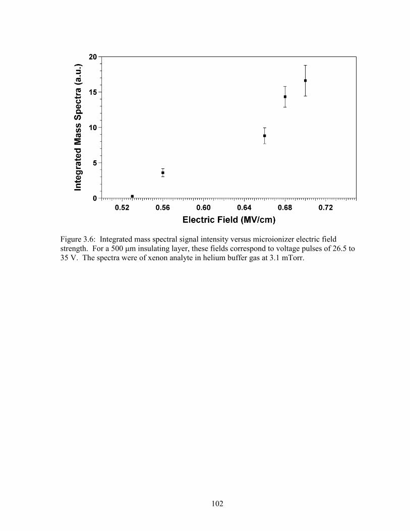
102
Figure 3.6: Integrated mass spectral signal intensity versus microionizer electric field
strength. For a 500 μm insulating layer, these fields correspond to voltage pulses of 26.5 to
35 V. The spectra were of xenon analyte in helium buffer gas at 3.1 mTorr.

103
Figure 3.7: Integrated mass spectral signal intensity versus microionizer bias potential.
Signal intensity generally increases with electron energy, however this data highlights the
inconsistent operation of the first generation microionizer. Spectra are xenon analyte in
helium buffer gas at 960 mTorr. The microionizer field strength was pulsed at 0.68 MV/cm
for 1 ms.

104
3.6 REFERENCES
1. Whitten, W. B., et al., High-pressure ion trap mass spectrometry. Rapid Commun.
Mass Spectrom. 2004, 18 (15), 1749-1752.
2. Wolfe, D. W. High-Pressure Cylindrical Ion Trap Mass Spectrometry. Dissertation,
University of North Carolina, Chapel Hill, 2012.
3. Blakeman, K. H., et al., High-Pressure Mass Spectrometry at Pressures Exceeding 1
Torr in a Microscale Cylindrical Ion Trap. Manuscript in preparation 2015.
4. Kornienko, O., et al., Micro ion trap mass spectrometry. Rapid Commun. Mass
Spectrom. 1999, 13 (1), 50-53.
5. Johnson, B. B., et al., Field ion source development for neutron generators. Nucl
Instrum Meth A 2012, 663 (1), 64-74.
6. Johnson, S., et al., Field emission properties of self-assembled silicon nanostructures
on n- and p-type silicon. Appl. Phys. Lett. 2004, 85 (15), 3277.
7. Srisonphan, S., et al., Metal-oxide-semiconductor field-effect transistor with a
vacuum channel. Nat Nanotechnol 2012, 7 (8), 504-508.
8. Huang, P. C., et al., High Efficiency and Smooth Transition Buck-Boost Converter
for Extending Battery Life in Portable Devices. 2009 IEEE Energy Conversion
Congress and Exposition, Vols 1-6 2009, 2342-2345.
9. Whaley, D. R., et al., 100 W Operation of a Cold Cathode TWT. Ieee Transactions on
Electron Devices 2009, 56 (5), 896-905.
10. Gilchrist, K. H., et al. In A Novel Ion Source and Detector for a Miniature Mass
Spectrometer, IEEE Sensors, 2007; pp 1372-1375.
11. Xu, N. S.; Huq, S. E., Novel cold cathode materials and applications. Mat Sci Eng R
2005, 48 (2-5), 47-189.

105
12. Felter, T. E., Cold cathode field emitter array on a quadrupole mass spectrometer:
Route to miniaturization. J Vac Sci Technol B 1999, 17 (5), 1993-1996.
13. Deheer, W. A., et al., A Carbon Nanotube Field-Emission Electron Source. Science
1995, 270 (5239), 1179-1180.
14. Kornienko, O., et al., Field-Emission Cold-Cathode EI Source for a Microscale Ion
Trap Mass Spectrometer. Analytical chemistry 2000, 72 (3), 559-562.
15. Fomani, A. A., et al., Toward Amp-Level Field Emission With Large-Area Arrays of
Pt-Coated Self-Aligned Gated Nanoscale Tips. Ieee Transactions on Electron Devices
2014, 61 (7), 2538-2546.
16. Hartley, F. T.; Kanik, I. In A nanoscale soft-ionization membrane: A novel ionizer
for ion mobility spectrometers for space applications, Proceedings of SPIE, The
International Society for Optical Engineering, 2002; pp 1-7.
17. Bower, C. A., et al., On-chip electron-impact ion source using carbon nanotube field
emitters. Appl. Phys. Lett. 2007, 90 (12), 124102.
18. Driskill-Smith, A. A. G., et al., The "nanotriode": A nanoscale field-emission tube.
Appl. Phys. Lett. 1999, 75 (18), 2845-2847.
19. Slade, P. G.; Taylor, E. D., Electrical breakdown in atmospheric air between closely
spaced (0.2 mu m-40 mu m) electrical contacts. IEEE T Compon Pack T 2002, 25 (3),
390-396.
20. Ono, T., et al., Micro-discharge and electric breakdown in a micro-gap. Journal of
Micromechanics and Microengineering 2000, 10, 445-451.
21. Cristoloveanu, S.; Li, S. S., Electrical characterization of silicon-on-insulator
materials and devices. Kluwer Academic: Boston, 1995; p 381.
22. Gomer, R., Field emission and field ionization. Harvard University Press:
Cambridge,, 1961; p 195.

106
23. Spindt, C. A., Microfabricated field-emission and field ionization sources. Surface
Science 1991, 266, 145-154.
24. Haynes, W. M., Handbook of Chemistry and Physics. 95th ed.; CRC Press: 2014; p
2693.
25. Sze, S. M.; Ng, K. K., Physics of semiconductor devices. 3rd ed.; Wiley-Interscience:
Hoboken, N.J., 2007; p 815.
26. Osburn, C. M.; Weitzman, E. J., Electrical-Conduction and Dielectric Breakdown in
Silicon Dioxide Films on Silicon. Journal of the Electrochemical Society 1972, 119
(5), 603-609.
27. DiMaria, D. J.; Stathis, J. H., Ultimate limit for defect generation in ultra-thin silicon
dioxide. Appl. Phys. Lett. 1997, 71 (22), 3230-3232.
28. Stuart, M., Conduction in Silicon Oxide Films. Brit J Appl Phys 1967, 18 (11), 1637-
1640.
29. Osburn, C. M.; Ormond, D. W., Dielectric Breakdown in Silicon Dioxide Films on
Silicon: II Influence of Processing and Materials. Journal of the Electrochemical
Society 1972, 119 (5), 597-603.
30. Osburn, C. M.; Ormond, D. W., Dielectric Breakdown in Silicon Dioxide Films on
Silicon: I Measurement and Interpretation. Journal of the Electrochemical Society
1972, 119 (5), 591-597.
31. Talin, A. A., et al., Field emission displays: a critical review. Solid-State Electronics
2001, 45 (6), 963-976.
32. Spindt, C. A., A Thin-Film Field-Emission Cathode. J Appl Phys 1968, 39 (7), 3504-
3505.
33. Ding, M. Q., et al., Fabrications of Spindt-type cathodes with aligned carbon
nanotube emitters. Appl. Surf. Sci. 2005, 251 (1-4), 201-204.

107
34. Kang, M., et al., Stable field emission from nanoporous silicon carbide.
Nanotechnology 2013, 24, 1-5.
35. Purcell, S. T., et al., Nanoprotrusion model for field emission from integrated
microtips. J Vac Sci Technol B 1997, 15 (5), 1666-1677.
36. Fursey, G., Field emission in vacuum microelectronics. Kluwer Academic/Plenum
Publishers: New York, 2005; p 205.
37. Stein, S. E., "Mass Spectra". in NIST Chemistry WebBook, NIST Standard Reference
Database Number 69 [Online] Linstrom, P. J.; Mallard, W. G., Eds. National Institute
of Standards and Technology, Gaithersbrug, MD, http://webbook.nist.gov, (accessed
10/2/2015).
38. Pau, S.; Whitten, W. B., Personal Communication. 2011.
39. Muller, E. W.; Bahadur, K., Field Ionization of Gases at a Metal Surface and the
Resolution of the Field Ion Microscope. Physical review 1956, 102 (3), 624-631.
40. Mathis, J. E.; Compton, R. N., Single and multiple photon ionization of triethylamine.
J Chem Phys 1996, 104 (21), 8341-8347.
41. Lu, K. T., et al., Toluene Cation - Nearly Free Rotation of the Methyl-Group. J Phys
Chem-Us 1992, 96 (24), 9742-9748.
42. Sielemann, S., et al., IMS with non radioactive ionization sources suitable to detect
chemical warefare agent simulation substances. International Journal of Ion Mobility
Spectrometry 2002, 5 (3), 143-148.
43. March, R. E., An Introduction to Quadrupole Ion Trap Mass Spectrometry. Journal of
Mass Spectrometry 1997, 32 (4), 351-369.
44. McLuckey, S. A., et al., Ion Trap Mass Spectrometry of Externally Generated Ions.
Analytical chemistry 1994, 66 (13), 689-696.
45. Jenkins, R. O., A Review of Thermionic Cathodes. Vacuum 1969, 19 (8), 353-359.

108
46. Blakeman, K. H. Development of High Pressure Mass Spectrometry for Handheld
Instruments. Dissertation, University of North Carolina at Chapel Hill, Chapel Hill,
NC, 2015.
47. Song, Q., et al., Ion trap mass analysis at high pressure: an experimental
characterization. J. Mass Spectrom. 2010, 45 (1), 26-34.
48. Huq, S. E., et al., Field emitters for space application. J Vac Sci Technol B 2001, 19
(3), 988-991.
49. Wu, S. M., et al., Sputtering yields of Ru, Mo, and Si under low energy Ar+
bombardment. J Appl Phys 2009, 106 (5).
50. Stuart, R. V.; Wehner, G. K., Sputtering Yields at Very Low Bombarding Ion
Energies. J Appl Phys 1962, 33 (7), 2345-2352.
51. Fowler, R. H.; Nordheim, L., Electron Emission in Intense Electric Fields.
Proceedings of the Royal Society A: Mathematical, Physical and Engineering
Sciences 1928, 119 (781), 173-181.
52. Andresen, R. D.; Page, D. E., On Ion Feedback in a Straight Channel Multiplier.
Nucl. Instrum. Methods 1970, 85 (1), 141-142.
53. Mark, T. D.; Dunn, G. H., Electron impact ionization. Springer-Verlag: Wien ; New
York, 1985; p 383.
54. Kauppila, W. E., et al., Measurements of total scattering cross sections for
intermediate-energy positrons and electrons colliding with helium, neon, and argon.
Physical Review A 1981, 24 (2), 14.
55. Asundi, K. K.; Kurepa, M. V., Ionization Cross Sections in He, Ne, A, Kr and Xe by
Electron Impact†. Journal of Electronics and Control 1963, 15 (1), 41-50.
56. Stephan, K.; Mark, T. D., Absolute partial electron impact ionization cross sections of
Xe from threshold up to 180 eV. The Journal of Chemical Physics 1984, 81 (7), 3116.

109
57. Bonard, J.-M., et al., Degradation and failure of carbon nanotube field emitters.
Physical Review B 2003, 67 (11), 115406.
58. Wei, Y., et al., Surface chemical changes on field emitter arrays due to device aging.
J Vac Sci Technol B 1999, 17 (1), 233-236.
59. Wallash, A.; Levit, L., Electrical breakdown and ESD phenomena for devices with
nanometer-to-micron gaps. Reliability, Testing, and Characterization of
MEMS/MOEMS II 2003, 4980, 87-96.
60. Kern, W., The Evolution of Silicon-Wafer Cleaning Technology. Journal of the
Electrochemical Society 1990, 137 (6), 1887-1892.
61. Kern, W.; Puotinen, D. A., Cleaning Solutions Based on Hydrogen Peroxide for Use
in Silicon Semiconductor Technology. RCA Review 1970, 31 (2), 187.
62. Reynolds, F. H., Thermally Accelerated Aging of Semiconductor Components.
Proceedings of the Ieee 1974, 62 (2), 212-222.
63. Levine, J. D., Benefits of the lateral resistor in a field effect display. J Vac Sci
Technol B 1996, 14 (3), 2008-2010.

110
CHAPTER 4: MICROIONIZER FABRICATION AND DEVELOPMENT
4.1 Introduction
The integration of the first generation microionizer with HPMS was considered
successful enough to warrant further development. Both positive and negative aspects of the
first generation’s performance were considered in designing subsequent ionizer generations.
The most important aspect of the initial integration was that it successfully generated ions for
HPMS. An ion source for HPMS must be small, low-power, and oxygen tolerant in
pressures upward of 1 Torr. The first generation with a small footprint achieved two out of
three objectives by generating mass spectra in high pressure air, but with high power
consumption and inconsistent performance from device-to-device. This chapter documents
an in-house developed fabrication process and improvements to both the device interface and
HPMS for lowering power consumption and increasing consistency of operation between
microionizers.
Thermal fluctuations in the first generation caused by high power consumption lead to
suboptimal performance in terms of achieving field ionization, device-to-device
reproducibility, and lifetime. The microionizer should behave as an ideal capacitor with only
displacement current and no leakage current. However, the first generation microionizer
easily pulled milliamp-levels of leakage current. There are several mechanisms responsible
for this leakage current into and through thin film dielectrics and they can be broken down
into either interfacial or bulk-related phenomena.1 Current and dielectric breakdown studies
of thin film insulators are most often considered in terms of field effect transistors where a

111
‘large’ device area is 0.0005 cm2.2 The microionizer, on the other hand, has a 1 cm
2 surface
area, thus insulator quality (bulk conduction) is paramount for reducing the leakage current.
Higher quality insulators offer fewer traps, defects, and ions for field-driven current
conduction.3-4
Given the encouraging field emission results of the first generation,
subsequent generations focused on reduction of leakage current through the choice of
insulating layer.
The initial microionizer was designed with simplicity in mind so that fabrication costs
could be held to a minimum. This fabrication approach relies upon deep reactive ion etching
(DRIE) and is straightforward compared with other field effect device fabrication methods.
DRIE utilizes a two-step process (passivation and etch) developed by engineers at Bosch,
GMBH.5 The Bosch process alternates passivation and etching to generate anisotropic
features with aspect ratios approaching 50.6 A single, simple field effect transistors (FET)
commonly requires an extensive process flow.7 Spindt-emitters for field emission have an
ever more complex flow due to the addition of arrays of carefully crafted field enhancing
tips.8-9
By contrast, the microionizer perforates a silicon-on-insulator (SOI) substrate using
DRIE and relies upon minor field enhancements of a macroscopically generated field
(~ 1 MV/cm) across the thin insulating layer. The surface roughness of the silicon sidewalls
at the interface of the insulating layer is responsible for the geometric enhancement necessary
to achieve 10 to 100 MV/cm electric fields.
The general process for fabrication of the first generation microionizer (Gen 1) is shown
in Figure 4.1a. The process starts with a SOI substrate consisting of three layers: device,
insulator, and handle. In step 1, a photoresist masking layer is deposited on the handle layer
and patterned via photolithography, defining an open window area (~ 1 mm2). 2) The

112
window is etched by DRIE into the handle to within approximately 20 μm of the insulator
layer after which the photoresist is stripped and the wafer cleaned. 3) A masking layer is
deposited on the device side and patterned with the active ionizer features and aligned with
the backside window using fiducial marks. 4) The wafer is through-etched from the device
side layer-by-layer: DRIE through the device layer; DRIE or wet chemical etch through the
insulator; and DRIE through the handle layer and finally, 5) the wafer is cleaned and diced.
A cross-section SEM of a completed device is shown in Figure 4.1b. The
device/insulator/handle layers form a membrane on the order of 25 μm thick. The device
layer (2 μm) and insulator (0.5 μm) are located at the top of the SEM. The active region is
the silicon-insulator interface with the handle layer for mechanical support. An optical image
of the front side of a 100 μm Gen 1 device is shown in Figure 4.1c. The color is due to
bonding fringes that are a result of optical interference from reflections off the insulating
layer.
Microionizer development at UNC using this process flow as a starting point was
undertaken and can be divided into three stages: Early, Optimization, and Final. Early
development focused on reproducing Gen 1 devices however with one departure from the
design – the through-etch. A single-side etch (starting at step 3 in Figure 4.1a) exposes the
silicon-insulator interface where field emission or field ionization occur. Etching through the
remainder of the handle layer would only act to enhance field ionization when forcing neutral
analyte molecules to pass through the active region (from handle to device layer) on their
way to the ion trap (rather than relying upon diffusion). Additionally, since Gen 1 devices
were only capable of field emission, etching through the handle layer is unnecessary. This
decision reduces the process development complexity and enhances the rate at which devices
113
can be produced and characterized. The Optimization stage was transitional as device
fabrication became consistent enough to produce microionizers with similar device-to-device
behavior improving characterization results. As part of the optimization process, the die
layout changed and electrical contact to the device and handle layers was made to the front of
the device. The through-etch was also attempted to determine the difficulties of
incorporating it with the front side processing. The lessons learned from these two stages
culminated in the Final development stage. The Final process was used to fabricate both
single-side and through-etch microionizers characterized for their leakage current and
emission intensity under HPMS conditions across an array of geometries and materials.
During the fabrication optimization time frame, the HPMS testing platform evolved as
well with improvements made through the combined efforts of the research group. Most of
the improvements have been documented10-11
and were used to maximum benefit for
microionizer development. A couple of advances regarding the development of a high
voltage pulsing circuit and vacuum chamber miniaturization are highlighted in this chapter
because they were crucial to successful implementation of the microionizer.
4.2 Fabrication
A full array of microfabrication tools, as detailed in Appendix 1, was available for device
development. Access to this equipment was crucial; from photolithography mask design and
fabrication to device processing up through to device bonding. Based upon the lack of field
ionization seen in the Gen 1 devices at ORNL, the first UNC devices were only front side
etched to just beyond the insulator layer. Since field emission is not dependent upon mass
transport of neutrals through the high field region, these microionizers should operate
similarly to the Gen 1 devices despite not being through-etched.

114
The first generation was defined as those devices fabricated at Arizona State University
while the additional generations developed at UNC were divided into the three stages of
fabrication: Early development (Gen 2 to 6), Optimization (Gen 7 and 8), and Final (Gen 9.1
to 9.6). A representative device from each generation is shown in Figure 4.2. Device
generations were numbered when either the photolithographic mask was updated or major
changes to the fabrication sequence were made. Table 4.1 displays substrate physical
characteristics for each microionizer generation. There were three categories of substrates
used for these studies: SOI (Ultrasil Corporation, Hayward, CA), polysilicon-on-insulator
(Pau Research Group, UA), and metal-on-insulator (Rogue Valley Microdevices, Medford,
OR). All substrates had four key features: the handle and device layers were always highly
doped; device layer thickness never exceeded 12 µm; the insulating layer was always less
than 1 µm thick; and the handle thickness was between 400 and 500 μm. The early
generations attempted to reproduce Gen 1 and remained faithful to those SOI specifications
until Gen 5, after which, device and insulating layer thicknesses were investigated. Thinner
device layers should yield improved signal intensity, while insulating layer thickness affects
the leakage current12
and operating voltage; 1.0 μm requires 100 V to generate 1.0 MV/cm.
The handle thickness balances robustness for handling and thin film stresses with etch time.
The handles were 10 to 30% thinner than normal for 100 and 150 mm diameter wafers.13
The material choice for each layer has consequences for device operation and fabrication.
Field emission is dependent upon the work function of a material;14
for silicon it ranges from
4.7 to 4.9 eV, depending on doping type and level.15
For reference, cesium has a work
function of 2.1 eV and can be coated on electrodes to enhance field emission from devices
but quickly degrades.16
Tungsten on the other hand, has a work function near 5 eV and is

115
used in high power devices because of its high melting point.17
Field emission from p-type
semiconductors is more complex than metals due to carrier inversion and field penetration.18
Both dopants were tested, but n-type silicon (> 1018
atoms/cm3) was the focus of this study
since it exhibits metal-like field emission.19
Internal crystal stress is influenced by the high dopant concentrations used, however the
insulating layer dominates the durability of the SOI structure.6 Silicon wafers less than
400 μm thick can actually warp under the stress induced by thin films such as oxide and
nitride. Wet, thermal oxides are preferred for bonded SOI because they grow quickly and
have residual ions for anodic bonding.20
However, they are prone to trapped charge states at
the silicon interface that can lead to charge conduction at high electric field strengths.21-22
As
such, alternatives were investigated including dry thermal oxide, oxide/nitride/oxide as well
as multi-layered, low-stress silicon nitride. Dry thermal oxide is of higher quality, yielding
higher dielectric breakdown than wet oxide.23
The layered materials were chosen because
the additional interfaces in the insulating layer suppress leakage current24
and with proper
annealing have lower stress than a single layer of insulating material of the same thickness.25
4.2.1 Early Development – Generations 2 to 6
Early development focused on reproducing Gen 1 devices for continued field emission-
based HPMS testing. As fabrication progressed towards Gen 6, the active ionizer feature
layouts changed to better align with the cylindrical ion traps (CIT) and stretched length ion
traps (SLIT) being developed in other parts of the HPMS program. The geometry of via
architecture also shifted away from the variety of circular features towards trench-only
layouts. A 10 μm trench width was chosen for superior etch results and to reduce variability

116
across the wafer. These devices adhered to the original design with the clamp-style holder
for electrical contact.
4.2.2 Optimization – Generations 7 through 8
Gen 7 and 8 were the first to depart from their predecessors in terms of device layout.
These also represent the first attempts at through-etching since Gen 1. These microionizers
used an ‘island’ configuration as seen in Figure 4.2g and h. The unused portions of the
device and insulator layers were removed to decrease the area available for leakage current
conduction. The island configuration encouraged a change in microionizer holder because
both device and handle layers could be accessed from the front side of the device. The
clamp-style holder was abandoned and printed circuit boards (PCBs) were employed. These
gave more flexible microionizer positioning relative to the CIT. The use of PCBs also helped
electrical contact evolve from silver epoxy to soldering and wire bonding.
4.2.3 Final Process – Generation 9
The optimization stage culminated in the final process and development of Gen 9
devices. The major steps of the final process flow can be found in Table 4.1. This process
blended every advance and lesson learned during fabrication, testing, and HPMS operation to
yield the microionizer as seen in Figure 4.2i. This design was overhauled such that the active
features, 10 x 90 μm2 trenches were laid out lengthwise in seven, 5 x 20 rectangular arrays.
Alignment was then ensured to overlap the 4 mm SLIT (an image of which is shown in
Figure 4.4a). The die layout was also changed to 2.5 x 20 mm2 in order to lay flat against the
compact ion trap electrodes.
Six versions of Gen 9 were fabricated, 9.1 to 9.6 with Figure 4.3a to f showing an optical
image of each. The first five versions were single-side etched starting at Step #8 in Table

117
4.2. These devices were fabricated to test the effect of device layer thickness, insulating
layer thickness, and material choice. Three variants were based on SOI substrates. The
remainder used layered substrates with cheaper material cost compared to bonded SOI:
metal-insulator-silicon and polysilicon-insulator-silicon. The final version, Gen 9.6, was
through-etched using the best performing substrate. The device layers of all variants except
9.3 and 9.5 are thin enough to be optically translucent. The colors and patterns observed in
Figure 4.3 are representative of the SOI bond quality, device layer thickness, insulating
material, and overall surface roughness. A Gen 9.6 device mounted and wire bonded to a
PCB is shown in Figure 4.3g. The die is secured to the PCB with epoxy before wire
bonding.
4.3 Experimental
4.3.1 HPMS Updates
Over the course of microionizer development, there were advances in nearly every aspect
of HPMS with most of these achievements incorporated into the microionizer test bed. One
key change that influenced the microionizer design was the miniaturization of the vacuum
chamber. This design was implemented to minimize parasitic capacitance for optimal CIT
operation at high frequencies (> 10 MHz) and was accomplished by reducing the ion trap
electrode surface area as well as the amount of coaxial cabling.11, 26
A comparison of an
original ion trap electrode next to a compact ion trap electrode is shown in Figure 4.4a where
the compact electrode has roughly half the surface area. The reduction in surface area
brought the mounting screws closer to the center (location of the ion trap), leaving only
3 mm between the heads of the mounting screws. This limited space required a redesign of
the microionizer, with the width of Gen 9 reduced from 10 to 2.5 mm. While both electrodes

118
can be used in the original HPMS differential chamber, shown in Figure 4.4b, only the
compact electrodes are compatible with the mini-chamber and the trap-mounted chamber as
shown in Figure 4.4c and d, respectively. The differential chamber was employed for the
external ion trapping results presented in Chapters 2; the first generation microionizer results
in Chapter 3, as well as testing Gen 2 through 7. The large volume of this chamber gave
great flexibility in experimental design. However, operation was often limited by discharge
(RF or DC) to the grounded chamber walls. The mini-chamber, shown in Figure 4.4c, was
used to test the 8th
generation microionizer. This chamber reduced the incidence of RF
discharge, easing mass analyzer operation, and reduced the gas loads on the pumping system
at the cost of flexibility.11, 26
The trap-mounted chamber, Figure 4.4d, was a purpose-built
version of the mini-chamber to provide room for the PCB mounted microionizer as well as
its associated electrical feedthroughs.
4.3.2 Microionizer Operation
While the ion traps and vacuum chamber received improvements, the majority of the
support electronics such as current preamplifier, data acquisition, and RF generation
remained constant throughout the testing of the microionizer. However, the pulsing circuit
received an overhaul between Gen 5 and 6. The original pulsing circuit relay was a simple
photorelay IC (PVA3354N) that was upgraded to a high-voltage single-pull, double-throw
switch (HV Switch). The HV Switch was custom designed and based upon N-channel
MOSFETS (Model STP6N95K5). The HV switch improved every aspect of voltage pulsing
over the optical relay – maximum amplitude (950 V versus 300 V), bias range (1 kV vs 300),
and ease of switching pulse polarity. The improvements are demonstrated in the oscilloscope
traces in Figure 4.5. The yellow traces are an 80 μs square, control pulse and the blue traces

119
are each circuit’s attempt to reproduce the control pulse with +125 V amplitude. The
photorelay response is shown in Figure 4.5a and shows a delay of 80 μs. More importantly,
it only outputs +88 V due to the slow rise time and requires over 200 μs to return to baseline.
Early microionizer operation used pulse lengths between 1 to 10 ms; at these time scales the
relay’s faults are evident but not disruptive to operation. As shorter pulse lengths were
investigated, a new pulsing circuit to overcome the photorelay’s limitations is required.
Figure 4.5b shows the performance of the HV Switch under the same operating conditions as
the relay. The HV Switch accurately reproduces the control pulse at +125 V amplitude, and
it displays a 200-fold decrease in rise time and a 1000-fold decrease in fall time compared to
the photorelay.
The mount interfacing the microionizer to the HPMS also evolved over the course of
development. A clamp-style holder previously discussed in Chapter 3 was used exclusively
with the differential chamber. As such, Gen 1 through 6 were tested with this style holder.
Beginning with Gen 7, the holder was updated to a PCB mount, three versions of which are
shown in Figure 4.6. The PCB shown in Figure 4.6a was used with Gen 7 and fabricated by
SAE Circuits Colorado, Inc. (Gunbarrel, CO). Electrical contact between the PCB and
microionizer was made by either silver epoxy, soldering, or copper tape. When the vacuum
chamber was switched to the mini-chamber, the PCB was updated as seen in Figure 4.6b.
This PCB was used as a vacuum bulkhead by an o-ring seal between the aluminum chamber
and PCB. The white, circular ring in the soldermask of the PCB was used to guide o-ring
placement when mounting the PCB to the vacuum chamber. The final version of the PCB
mount is shown in Figure 4.6c and used wire bonding to make electrical contact. Fabrication
was by Sierra Circuits, Inc (Sunnyvale, CA) for their superior, wire-bondable gold finish. It

120
was mounted in the vacuum chamber as shown in Figure 4.4d. The spacing between the
microionizer and SLIT could be controlled to 50 μm.
4.3.3 Characterization and Testing
Fabrication results were primarily assessed in three ways: profilometry (P-6 Stylus
Profilometer, KLA-Tencor); optical microscopy (VHX-2000, Keyence Corporation and
Eclipse LV-150, Nikon Corporation); and SEM (FEI Quanta 200 ESEM or FEI Helios 600
Nanolab, FEI Corporation). Any reference to physical dimensions such as etch depth was
measured with one or more of these techniques. Profilometry and optical microscopy were
crucial for monitoring etch depth to gauge DRIE etch rates. Additional observations by SEM
were critical in determining a number of device physical attributes including: the fidelity of
the final etch features with the mask; notching at the silicon-insulator interface; and surface
roughness.
Both field emission and field ionization used 1 ms voltage pulses, a 3.6% duty cycle. An
operational schematic is shown in Figure 4.7a using an SEM image to highlight how the
voltages are applied to the device as well. For field emission, the microionizer was pulsed
and biased negatively; positive mode reversed the polarities of the pulse and bias. The
voltage pulse generates the electric field across the insulating layer while the bias voltage
aids in extracting the charge once emitted. Figure 4.7b shows a high-magnification SEM of
the surface roughness of the handle layer at the insulator-handle interface. This roughness is
likely responsible for the geometric field enhancement necessary to achieve field emission
and field ionization. The voltage pulse was monitored using an oscilloscope (Model
DPO3034, Tektronix, Inc), while the bias was measured with a digital multimeter (Model
179, Fluke, Inc). The pulse and bias supplies were ballasted with 100 kΩ and 1 MΩ

121
resistors, respectively. Average current was measured via digital multimeter (Model
U1272A, Agilent, Inc.) operated in DC-Current mode on the μA scale. Microionizer
operation was characterized under HPMS conditions as both a field emission and field
ionization source. Air was leaked into the ionization-side chamber with a needle valve, and
the pressure measured ranged from 350 to 1000 mTorr. A schematic of the ionizer test setup
is shown in Figure 4.8. The ionizer was spaced approximately 100 μm from a voltage-
controlled aperture electrode. The aperture mimicked a SLIT with xo = 100 μm and length =
4.0 mm and was controlled between ± 250 V. The aperture throttled gas flow into the
detection chamber, keeping the EMT chamber pressure below 100 mTorr. Signal was
detected using an EMT (Model 2300, Detech, Inc.) biased to -1200 V; the output of which
was amplified (2 nA/V) by a current preamplifier (SR570, Stanford Research, Inc). In
positive mode, the detected signal was a direct measure of the microionizer’s emission. In
field emission mode, the signal was a measure of the ions generated via EI, where the rate of
ion generation was assumed to be proportional to the field emission intensity.27
Ambient air
provided the background neutrals for both modes of operation. Signal was acquired at
250 kHz using the same interface described in Chapter 2. It was averaged over 250 scans,
low pass filtered at 30 kHz, and integrated to produce data points for plotting purposes.
4.4 Results and Discussion
4.4.1 Fabrication and Leakage Current
The final process flow described in Table 4.2 evolved from the lessons learned
fabricating Gen 2 through Gen 8 microionizers. In the Early development phase, these
lessons pertained to developing and optimizing silicon microfabrication techniques.
Eventually, procedure refinements led to reproducible device performance (Optimization

122
phase) and progressed towards the final process flow. While many lessons were learned, two
dealing with DRIE and final device preparation in particular were crucial to success.
Deep reactive ion etching (DRIE) is a well-established technique in micro-electrical-
mechanical systems (MEMS).28-29
However, its implementation is highly specific to the
fabrication tool, the loading area of the pattern, and masking material employed. In the Early
and Optimization stages of device development, broken wafers in the DRIE were a common
occurrence. Many reasons were posited: seeking to maximize yield the early mask design
patterned the entire wafer; thinned wafers lacked robustness; and the thin films in use
(chromium masking, SiO2 insulators, etc.) simply added too much stress to the wafer causing
it to break. While any combination of these issues could have contributed to wafer breakage,
the real culprit was heat. When optimized, a 100 μm etch depth required 14 min of etch time
at approximately 7 μm/min. The ceramic mechanical chuck of the Alcatel AMS-100 DRIE
was unable to adequately remove the heat generated during this etch time, resulting in mask
degradation and wafer breakage. This overheating was overcome by adding a delay step to
the etch process. The final etch was a loop of 30 s of Bosch etch followed by 60 s of dead
time, yielding an effective etch rate near 4 μm/min. The heat released during etching is
dissipated in this 60 s dead time, greatly increasing the selectivity of the masking material
(particularly towards the perimeter) and reducing the risk of wafer breakage. For reference,
15 wafers were processed for Gen 2 through 8 with most of these wafers suffering breakage
during the etch process, primarily due to thinning at the perimeter. Whereas, Gen 9 that
utilized the delay loop, had no wafers broken during the DRIE step. Moreover, most wafers
retained sufficient structural rigidity for the follow-up wet cleaning, contact pad deposition,
annealing, and dicing.

123
The second major obstacle overcome during development was the device to HPMS
interface. Gen 1 through 6 utilized a clamp style holder, mainly because it was simple and
the ionizers were capable of producing mass spectra and their inconsistent performance was
thought to be a result of insulator quality. Only when the device layout was updated for Gen
7 and 8 and electrical contact made by wire bonding was poor electrical contact determined
as a major issue. The disadvantage of the clamp-style holder is evident in Figure 4.9 where a
comparison of current draw versus field strength for clamp-style contact and wire bonded
contact is shown. The black squares in Figure 4.10a are a Gen 5 device that used the clamp-
style holder and have current draws above 0.5 mA. The leakage current however was held in
check using a low duty cycle (less than 1%) and by current limiting the power supply to
4 mA. The wire bonded Gen 8 (red squares) and Gen 9 (blue squares) generation devices
both have a dramatic drop in leakage current compared to the clamped-style Gen 5 device.
Figure 4.10b shows a magnified view of these results. Relative to the maximum current of
Gen 5, Gen 8 is 2500-fold lower and Gen 9 is over 11,000-fold lower. Moreover, higher
duty cycles are possible – the Gen 9 trace used a 22% duty cycle; thus increasing the mass
spectral acquisition rate by more than 3-fold to 44 Hz. The current draws shown in these
traces are also closer to what is expected from a FED30-31
and are directly attributable to
electrical contact by wire bonding.
Examples of wire bonds used with Gen 8 and 9 devices are shown in Figure 4.10. In
manufacturing, wire bonding is a staple for establishing stable electrical contact to silicon
dies.32
It requires a metallized, contact pad be deposited onto the silicon surface. Bonding is
achieved with thermosonic compression – a combination of ultrasonic agitation,
compression, and heat welds the wire to the contact pad. The pad material must be chosen

124
such that it creates an ohmic contact with the silicon while also alloying with the wire.32-33
The bond system used in Gen 8 shown in Figure 4.10a were titanium/copper contact pads
with 1 mil aluminum wire bonded to the front and back side pads.34
Figure 4.10b shows a
Gen 9 bond system with titanium/palladium/gold metallized pads and 1.5 x 0.5 mil2 gold
ribbon.35
The drastic reduction in current draw introduced by wire bonding suggests that the
‘leakage’ current had less to do with the insulating layer than the electrical contact. The
likely candidate for the intermittent electrical contact with the clamp-style holder would be
the native surface oxide.36
The clamp-style holder likely functioned when a perfect balance
of surface abrasion and clamp pressure was attained.
Microionizer development progress accelerated once the fabrication and electrical contact
procedures were established such that wafer-level failure analysis was possible. Six variants
of Gen 9 were produced, with a sample completed wafer shown in Figure 4.11a. The Gen 9
mask produces 208 devices from a single, 150 mm wafer. Operable vs. non-operable devices
are distinguished by measuring the microionizer’s capacitance, with operable devices
measuring nF capacitance and non-operable devices measured as short circuits. Thirty
devices from a wafer processed for a single variant were chosen at random across and
measured. The device yield and average capacitance categorized by variant were determined
and are shown in Figure 4.11b. Gen 9.2 and 9.4 both show sub-standard yields compared to
the others with only 43 and 73% yields, respectively. The probable cause for the low yield is
that both Gen 9.2 and 9.4 have polySi device layers. SOI is a very reliable substrate, but it is
also expensive from a manufacturing standpoint so alternatives were explored. Thin polySi
films can be sequentially deposited on wafers in a parallel fashion reducing costs, while SOI
wafers requires an anodic bonding step performed on single wafer-to-wafer pairs. The

125
polySi wafers pushed the boundaries in terms of maximum insulating layer thickness
(300 nm, dry-thermal SiO2 for Gen 9.2 and 1000 nm Si3N4 for Gen 9.4) to try and minimize
the leakage current when it was thought to be a result of insulating layer quality.
Unfortunately, the stresses in these thin films when combined with that of the poly-Si device
layer, which was deposited at 0.5 μm thicknesses, resulted in fragile wafers. As a result, the
fabrication process for these two variants consumed multiple wafers due to breakage during
the lithography steps. Lithography is an early process step and breaks at this point are
unusual from a MEMS perspective, suggesting the thin-film induced stress was very high for
these substrates. Moreover, successfully fabricated devices broke down and shorted before
any significant ion current could be collected with some even showing visible fractures after
testing. Due to their poor yield, these devices were not further characterized.
Despite the failures of the polySi-based devices, the remaining Gen 9 devices provided
insight into the operation of the microionizer. Gen 9.5 had a titanium/chromium device layer
on oxide that was investigated as another alternative to SOI. The remaining variants, Gen
9.1, 9.3, and 9.6 were based upon Ultrasil SOI. The key features and main differences
between each variant are listed in Table 4.3. Briefly, Gen 9.1 was the first wafer to use the
trap-mounted configuration as well as gold wire bonding. Gen 9.3 used the same substrate
SOI as 9.1, only the device layer was left unaltered at 10 μm. Gen 9.6 also used the same
substrate SOI and was meant to be as similar as possible to Gen 9.1 only with a through-etch.
Gen 9.5 had the thinnest device layer and insulator of the 4 variants at 0.25 and 0.3 μm,
respectively.

126
4.4.2 Field Emission Mode Operation
The field emission signal intensity as a function of field strength is shown for each 9th
generation microionizer in Figure 4.12. The data was collected at 1 Torr of room air buffer
gas in a gated configuration (as shown in Figure 4.8). The electric field range varied from
device to device, beginning where measurable emission was observed and ending short of
electrical discharge. The raw signal intensity is shown in Figure 4.12a. As expected for a
field emission source, the signal of all four devices increases exponentially with field
strength.37
To highlight this fact, the data is reevaluated in Fowler-Nordheim coordinates
and shown in Figure 4.12b. The linear relationship indicates Fowler-Nordheim tunneling is
responsible for the electron emission; assuming that the ions detected by the EMT are
directly proportional to the field emission intensity. For a well-defined field emission tip
(radius of curvature and aspect ratio), these plots can be used to estimate the emission area
and geometric field enhancement of the device, but that would be improper for the
microionizer because the emission sites are not well defined.38
Returning to Figure 4.12a, a range of maximum field emission strengths is observed
among the variants. Gen 9.5 has the largest overall signal intensity as well as the thinnest
insulating layer at 0.3 μm and the thinnest device layer at 0.25 μm. It produced a measurable
signal at 1.0 MV/cm and a slow emission ramp over 0.8 MV/cm. Gen 9.3 had the next
largest signal intensity and a 1 μm insulating layer and 3 μm device layer. It ranged from 1.4
to 1.8 MV/cm. Gen 9.6, which should be identical to Gen 9.1 except for the extra processing
required to fabricate a through-etch; demonstrated moderate field emission at the highest
field strengths observed, 1.8 to 2.2 MV/cm. Finally, Gen 9.3 showed a small amount of field
emission from 1.5 and 2.0 MV/cm. This device should be identical to Gen 9.1, except with a

127
10 μm device layer. The observed signal intensity of Gen 9.3 was over 24-fold lower than
Gen 9.1, suggesting that the device layer thickness plays an important role in charge
extraction from the microionizer. Given the operating conditions, this is not surprising. The
device layer is a field-free region, and electrons must drift through it. Any interactions will
remove energy and reduce the electron’s probability of transiting this region. Another factor
that may contribute to this drop in signal is the angular dependence of the field emission.37
Thus, the device layer may serve to ‘clip’ signal that does not exit the emission site
orthogonal to the silicon surface.
The difference in both signal intensity and field strength between Gen 9.1 and 9.6 was
unexpected because the insulating layers were identical and device layer thickness near 3 μm
for both. Gen 9.6 showed a 4.8-fold reduction in maximum signal intensity, while requiring
a 22% higher field strength to achieve it. The measured device layers of the two variants are
2.6 μm for Gen 9.1 and 3.1 μm for Gen 9.6. While there is a 20% difference in device layer
thickness, this alone should not account for the entire disparity in signal intensity, given that
a 400% difference between Gen 9.1 and 9.3 yielded a 24-fold decrease in signal intensity.
Moreover, device layer thickness should not contribute to the increased field strength
required in Gen 9.6. The SEMs of Gen 9.1 and Gen 9.6 shown in Figure 4.13 reveal a major
difference at the insulator interface. The device layer of Gen 9.6 was notched nearly 1.5 μm
from the edge of the insulating layer. This notching was likely a result of the through-etch
since the other Gen 9 variants do not display it (images not shown). The overhanging
insulating layer likely acts to hinder field emitted electrons from exiting the device. Thus,
the larger field strength needed for emission was likely required to overcome this
inefficiency. Unfortunately, this insulating layer contains a nitride which is difficult to wet

128
etch39
without affecting the silicon or wire bonding pads. A pure oxide could be etched back
with a simple buffered oxide etch which might then shift the field strength range back in-line
with Gen 9.1.
The maximum field strengths possible are limited by electrical discharge, which is
observed as an overload of signal from the electron multiplier. Comparisons of the
maximum field strengths generated for each variant lend insight into the discharge
mechanism. Insulator breakdown was unlikely because the ballast resistors prevent current
surges capable of instantly breaking down the insulator. Moreover, after the field limit was
found, each device was operated for at least 1 hour afterwards with no signs of signal
degradation or increased leakage current. Thus, discharge is likely a result of a
microdischarge plasma aided by surface flashover.40-41
In a microdischarge, field emission
typically contributes to atypical Paschen breakdown by generating ions (via EI) in the gap
between electrodes, which in this case is the insulating layer. Gen 9.1 and 9.5 each had
maximum field strengths near 1.8 MV/cm, while still producing a strong signal, meaning
there is sufficient charge in the vicinity to generate a discharge pathway. However, Gen 9.3
and 9.6 have the same insulating layer as 9.1 but discharge limits that are 11 and 22% higher
than 9.1. The thick device layer of 9.3 likely acted as a charge sink, suppressing the
conditions for flashover and neutralizing a portion of the ions generated via EI in the vicinity
of surfaces. Gen 9.6 has a nearly identical device layer thickness as gen 9.1 and the highest
limit on discharge field strength. This is likely due to a geometric suppression of the surface
flashover by the notch seen in Figure 4.13b.42
While the notch was not planned for, it may
have shown a way to intentionally design the microionizer to sustain higher field strengths at
the cost of field emission current.

129
The plots in Figure 4.14 show further evidence of the microionizer working as a field
emission source. The results of a gating experiment are plotted in in Figure 4.14a for a Gen
9.5 microionizer at 1 Torr. The field strength was held constant at 2.0 MV/cm by applying a
voltage of -60 V across the 0.3 μm insulating layer. An additional bias of -25 V was applied,
therefore the maximum kinetic energy of the electrons leaving the surface of the emission
source was -85 eV. As the gate potential was changed from 0 to -75 V, the signal decreases
to zero, indicating the microionizer is a source of negative charge. It is important to note that
the EMT detects positive ions, thus the loss in signal is because electrons arriving at the gate
electrode no longer have sufficient energy to perform EI. This conclusion is also consistent
with the mass spectrometry-based results shown in Chapter 3.
While field emission has been demonstrated, one key aspect has been ignored, power
consumption. Figure 4.14b plots each Gen 9 microionizer’s average current draw as a
function of field strength. All four variants demonstrate a similar improvement in leakage
current over the Early stage microionizers as shown in Figure 4.9. In particular, Gen 9.1 and
9.5 demonstrated their maximum field emission strengths at 1.8 MV/cm, which required
voltage pulses of -180 and -55 V, respectively. The corresponding current for each was 0.6
and 0.2 μA; yielding an average power consumption of 110 and 11 μW. With a duty cycle of
3.6% (1 of 28 ms), the peak powers were 3.0 and 0.3 mW. An important note is the
amplitude of Gen 9.5. It had the thinnest insulating layer and was able to operate at only
55 V of amplitude. This low power consumption is advantageous for use in a portable
instrument that most likely will be powered by a battery. In comparison to the alternative
glow discharge ionization source operating at 1 Torr of air under identical duty cycle
conditions, the GD source runs with a pulse of 625 V and draws 35 μA, yielding average and
130
peak powers of 21.8 and 605 mW. The glow discharge consumes over 1900 times more
power than the microionizer.
4.4.3 Positive Mode Operation
Positive mode operation is believed to produce field ionization. Early stage devices were
periodically operated in positive mode operation but the insulating layers typically suffered
fatal breakdown before ion generation was observed. This breakdown was believed to be a
consequence of the high leakage current combined with the increased field strength required
for field ionization versus field emission. With the reduced leakage current of the Gen 9
devices, positive mode operation was revisited. Using the same experimental setup as
described in Figure 4.8, the polarity of the pulse and bias voltages were reversed with the
results plotted in Figure 4.15. Signal intensity as a function of field strength is shown in
Figure 4.15a for each Gen 9 device. The applied electric field was investigated from
observable signal to values just shy of electric discharge. Ambient air was leaked into the
chamber to monitor ionization and assumed to be constant with time. Each device shows an
exponential increase in signal strength with the electric field. This behavior is expected
under low-field conditions near the threshold for field ionization. For a single analyte at low
pressures (< 0.1 mTorr), one would expect to see signal plateau as the probability of
ionization approaches one.43
However, the atmospheric sample is a mixture and each
compound has a different ionization potential. Thus signal is not expected to plateau under
these conditions. The current draw and power requirements under positive mode were also
similar to field emission mode. The largest average current was measured at 2.7 μA for Gen
9.6, yielding average and peak power of 0.68 mW and 18 mW, respectively.

131
The results of a gating experiment performed in positive mode are shown in Figure 4.15b.
The experiment is identical to that shown in Figure 4.14b, except a positive gate voltage was
used to block the ion current. The gating experiment was performed with a Gen 9.5 device,
pulsed with +70 V for an electric field of 2.3 MV/cm. An additional +25 V bias yielded a
maximum ion kinetic energy of +95 eV. The signal dropped to zero as the gate potential
increased from ground to +90 V. These results are consistent with ion generation occurring
at the microionizer. However, it cannot differentiate whether the ion current is a result of
field ionization or electron impact ionization.
The mechanism behind positive ion mode is believed to be field ionization though the
gate aperture experiment cannot distinguish how the ions are generated – by direct field
ionization or EI localized near the microionizer’s surface. The electric field strength
necessary for field ionization should be five to ten times greater than field emission, however
for the microionizer this is not the case. For an emitter with well-defined geometry (radius of
curvature and aspect ratio), an enhancement factor can be calculated assuming the work
function is known. When the emission site is not defined as in our case, only a rough
estimate of the enhancement can be made.44
Theoretically, field emission should initiate at
10 MV/cm though it can range as high as 50 MV/cm for higher work functions.18, 37
The
microionizer initiates field emission near 1.4 MV/cm, thus a field enhancement factor is
estimated at 8 to 35. The field ionization threshold also depends upon the ionization
potential of an analyte.43
Many compounds of interest (VOC, CWA, and explosives) have
ionization potentials from 7 to 12 eV.45
The threshold field strengths of these compounds are
closer to 50 to 70 MV/cm.46-47
Positive mode operation only requires a 10 to 50% increase in
field strength (relative to field emission) to generate ions, yielding an estimated field

132
enhancement of 25. Because field emission and field ionization sources can operate with less
than an order of magnitude between the modes,48
the exact mechanism under positive mode
operation is not known. To fully determine the mechanism, HPMS experiments looking at
ion generation are needed.
4.5 Conclusions
The first generation microionizer produced mass spectra under HPMS conditions –
showing that the microionizer design could operate in an oxygen-containing environment at
1 Torr. However, it failed one important test: low power operation. The mA-level leakage
current was thought to negatively impact device-to-device reproducibility, signal intensity,
and access to field ionization mode. This chapter documented the development from mask to
device testing of a process flow that is capable of producing through-etched microionizers.
The leakage current was reduced to the μA-level by combining proper metal-semiconductor
contact pads with wire bonding. The microionizer demonstrated consistent operation from
day-to-day and device-to-device, enabling studies of field emission and positive mode
operation for several Gen 9 variants. Each variant demonstrated field emission confirmed by
Fowler-Nordheim and gating experiments, as well as a positive mode of operation confirmed
via emission studies and gating. The variants demonstrated that a thin device layer is key to
charge extraction. The best performing variant, Gen 9.1, had high fabrication yield with
consistent field emission and positive mode operation. The mechanism behind positive mode
operation could not be confirmed as either field ionization or device-localized electron
impact ionization. Regardless, the microionizer demonstrated its utility as a dual-role
ionization source. Moreover, it did so under all the requirements for portable, HPMS: 1 Torr

133
of atmospheric buffer gas and low power. Lifetime and mass spectral-level signal intensity
are investigated in Chapter 5 documenting microionizer use with HPMS.

134
4.6 Figures
Figure 4.1: a) Process flow steps for Gen 1 devices beginning with a prime SOI substrate
with device, insulator, and handle layers. 1) Handle layer mask is deposited and
photolithographically patterned. 2) DRIE of handle layer window features as seen in b). 3)
Resist is stripped and wafer cleaned, then the device layer mask is deposited before
photolithographically defining the active features. 4) Device layer etch using DRIE for
silicon and/or wet etch for insulating layer. 5) Masking removed and wafer cleaned before
dicing. b) Cross-sectional SEM of the membrane produced by the fabrication process. The
location of the silicon-insulator interface of the SOI is near the device layer and the
supporting handle layer has been thinned to ~ 25 μm. c) Optical image of the device layer of
a completed 100 μm diameter Gen 1 device.

135
Figure 4.2: Optical image of representative microionizers. The three eras of development
from UNC Chapel Hill are highlighted: Early (); Optimization (); and Final (). a) Gen 1,
100 μm radius features b) Gen 2, 100 μm radius features c) Gen 3, 10 x 90 μm2 trench d) Gen
4, 10 x 90 μm2 trench e) Gen 5, 10 x 90 μm
2 trench f) Gen 6, 3-SLIT array of 10 μm width
trenches g) Gen 7, 19-element, CIT array of 10 μm width trenches h) Gen 8 with identical
elements as Gen7. The device layer is expanded (relative to Gen 7) to facilitate device layer
electrical contact. i) Gen 9, single-SLIT compatible 10 x 90 μm2 trenches. Early generations
mimicked the Gen 1 with 5, 20, and 100 μm circular features as well as 5 x 90 μm2 trenches.
Subsequent generations used only trench features, 10 μm in width of varying lengths that
were arrayed to match the ion traps’ layout. Gen 1, 7, 8, and 9 were all through-etched.

136
Device Insulator Handle
Generation(s) Type
Diameter
(mm)
Type
(Dopant)
Thick
(μm) Type
Thick
(μm)
Si
(Dopant)
Thick
(μm)
1 SOI 100 Si (Sb) 2 Oxide 0.5 Sb 400
2, 3, 4 SOI 76.2 Si (Sb) 2 Oxide 0.5 Sb 400
5.1 SOI 100 Si (Sb) 12 Oxide 0.5 Sb 450
5.2 SOI 150 Si (B) 5 Nitride 0.5 B 600
6, 9.1, 9.3, 9.6 SOI 150 Si (Sb) 10 Ox/Ni/Ox 0.4/0.3/0.3 Sb 450
7 Alt 150 Ti/Cr 0.015/.25 Nitride 0.6 B 500
8.1 SOI 150 Si (B) 5 Oxide 1 B 500
8.2, 9.5 Alt 150 Ti/Cr 0.015/.2 Oxide* 0.3 Sb 420
8.3, 8.4, 9.4 Alt 150 PolySi (As) 0.5 Nitride 1 Sb 450
9.2 Alt 150 PolySi (As) 0.5 Oxide* 0.3 Sb 420
Table 4.1: Substrate characteristics for each generation of microionizer.
* denotes dry, thermal oxide. Alt = alternative to SOI. All silicon is single-crystal, <100> unless specified.

137
Step # Wafer Side Description Fab Tool Notes
1 Back Ti/Cr Mask Deposition e- Beam Pump down at least 4 h
2 Back Photolithography - AZ9260 Resist Lithography Spin Coater/Mask Aligner. Resist thickness 7 µm.
3 Whole Chrome etch N/A Transfer resist pattern into the chrome mask
4 Back Isotropic Si etch of backside windows RIE 375 µm etch depth
5 Whole Heated Nanostrip 2X N/A Strip any remaining organics
6 Whole Chrome etch N/A Strip chrome mask
7 Whole RCA Cleaning N/A Remove particles, organics, and metals
8 Front Photolithography - AZ9260 Resist Lithography Double-side aligned. Resist thickness 7 µm.
9 Front Anisotropic Si etch of device layer DRIE Etch is looped for 30 s on and 35 s off. Depth
depends on device layer thickness
10 Front Anisotropic Insulator etch DRIE Etch is looped, mainly a physical sputtering
11 Front Anisotropic Si etch of handle DRIE Same etch as device layer, ~75µm depth
12 Front Oxygen plasma clean DRIE Strip photoresist
13 Front Anisotropic Si etch, thin device layer DRIE Same etch as device layer, aiming for < 3 µm device
layer thickness
14 Front Oxygen plasma clean DRIE Strip leftover passivation fluoropolymer
15 Whole Heated Nanostrip 2X N/A Strip any remaining photoresist
16 Whole RCA Cleaning N/A Remove particles, organics, and metals
17 Front Ti/Pd/Au electrical contact deposition e- Beam Pump down at least 5 h. Contact pads defined by
kapton shadow mask (< 100 µm thick)
18 Whole Anneal contacts at 450o C Furnace Under forming gas to prevent oxidation
19 Whole Dicing Dicer Diced completely, 2 cuts/street
20 N/A Affix die to PCB with epoxy Oven EpoTek LHC epoxy
21 N/A Au-Ribbon Bonding Wire Bonder Ribbon is 0.5 x 1.5 mil2
Table 4.2: Final process flow from wafer to microionizer.

138
Figure 4.3: Optical images of 9th generation silicon dies (2.5 x 20 mm2). a) through f) are
Gen 9.1 to 9.6, respectively. g) Image of a wire-bonded Gen 9.6 microionizer. Gen 9.1 to
9.5 are single-side etched. Gen 9.6 is a through-etched version of the best performing
variant, Gen 9.1. The active features for all six variants are 5 x 90 μm2 trenches. The
circular features are gold wire bonding pads deposited by e-beam evaporation. The pad at
the bottom of each device is for handle layer electrical contact, the remaining pads are for
device layer contact.

139
Figure 4.4: Evolution of the HPMS. a) Image of the SLIT ring electrodes used. The full-
size electrode (left) was used in the differentially pumped system while the compact
electrode (right) was compatible with all versions of the HPMS. b) Original differentially
pumped chamber used for Chapter 2 and Chapter 3 experiments. The labeled features: 1, 2,
and 3, highlight the ionization source, mass analyzer, and detector, respectively. c) The
mini-chamber, shown with an electron multiplier detector housing. The SMA feedthroughs
are vacuumed sealed and soldered directly to the ion trap. d) A microionizer-specific
variation of the minichamber; the trap-chamber volume was adapted to include the entire
microionizer-PCB-SLIT assembly.

140
Figure 4.5: Oscilloscope screen shot of voltage pulse generation by the a) PVA 3354n relay
and b) the Single-Pull, Double-Throw High-Voltage Switch. The control pulse () for both
circuits is 80 μs TTL. The output () pulse is each circuits’ attempt to reproduce the control
pulse at +125 V amplitude. While the relay has an inherent delay of about 80 μs, the real
problem is in the rise and fall times that are longer than the pulse length, preventing the pulse
from achieving full amplitude. The HV Switch has virtually no delay as well as 200 to 1000-
fold faster rise and fall times.

141
Figure 4.6: Evolution of the microionizer PCB mount. 1 and 2 refer to device layer and
handle electrical contact locations, respectively. a) The PCB was used with Gen 7 inside the
differential chamber. A wire was soldered at point 1, which would then be silver
pasted/epoxied to the front side of the device. b) The mini-chamber compatible PCB used
with the Gen 8 microionizer. It was with wire/epoxy bonding as well as wire bonding. c)
The trap-mounted microionizer PCB exclusively used for Gen 9 and designed for gold wire
bonding. The bond pads are approximately 1.5 cm from the ionizer features in order to clear
the ion trap electrodes when laid face-down for trap mounting.

142
Figure 4.7: a) Cross-sectional SEM of Gen 9.3 device, the bias and pulse voltages are
schematically shown. Field emission uses negative bias and pulse, while positive mode uses
positive polarity. b) High-resolution SEM of field enhancement sites.

143
Figure 4.8: Schematic of the ionizer test setup (not to scale). An aperture was used to
maintain differential pressure between two chambers, ionization and detector. The
microionizer and aperture were operated at high pressure (~ 1 Torr) and the EMT detector
was held at low pressure. The spacing between the ionizer and aperture was 100 μm, and the
aperture was electrically isolated in order to be used as a gate electrode.

144
Figure 4.9: a) Representative current draws as a function of electric field strength for three
generations of microionizers: Gen 5 (); Gen 8 (); and Gen 9 (). b) A magnified view of
Gen 8 and Gen 9 results. These traces were recorded in field emission mode and the duty
cycles were 0.1, 0.2, and 4.43%, respectively.

145
Figure 4.10: Images of a) Gen 8 wire bonds utilizing 1 mil diameter aluminum wire and
titanium/copper bond pads and b) Gen 9 wire bonds consisting of 0.5 x 1.5 mil2 gold ribbon
and titanium/palladium/gold bond pads.

146
Figure 4.11: a) Image of processed Gen 9.6 wafer. b) Results of wafer-level failure analysis.
The Gen 9 mask afforded 208 devices per 150 mm silicon wafer. The capacitance of 30
devices from each variant was measured to determine the fabrication yield and average
capacitance. Low yields were the result of shorted devices, likely due to stress fractures in
the insulating layer.
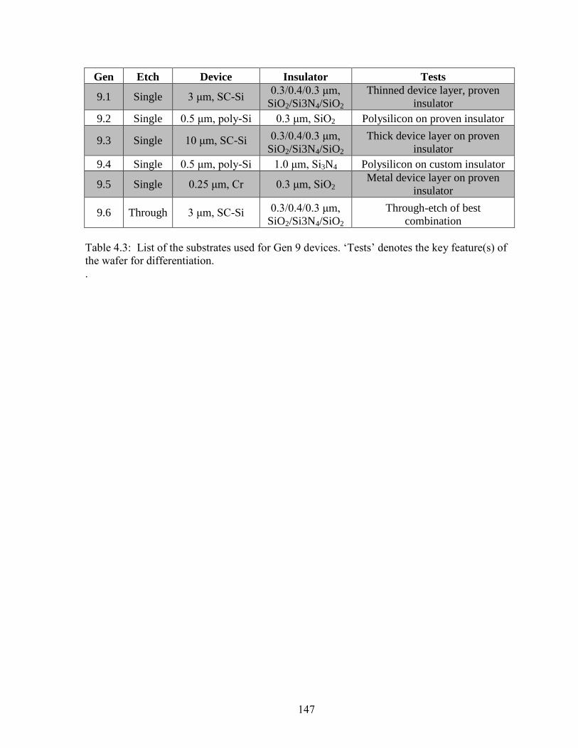
147
Gen Etch Device Insulator Tests
9.1 Single 3 μm, SC-Si 0.3/0.4/0.3 μm,
SiO2/Si3N4/SiO2
Thinned device layer, proven
insulator
9.2 Single 0.5 μm, poly-Si 0.3 μm, SiO2 Polysilicon on proven insulator
9.3 Single 10 μm, SC-Si 0.3/0.4/0.3 μm,
SiO2/Si3N4/SiO2
Thick device layer on proven
insulator
9.4 Single 0.5 μm, poly-Si 1.0 μm, Si3N4 Polysilicon on custom insulator
9.5 Single 0.25 μm, Cr 0.3 μm, SiO2 Metal device layer on proven
insulator
9.6 Through 3 μm, SC-Si 0.3/0.4/0.3 μm,
SiO2/Si3N4/SiO2
Through-etch of best
combination
Table 4.3: List of the substrates used for Gen 9 devices. ‘Tests’ denotes the key feature(s) of
the wafer for differentiation.
.

148
Figure 4.12: a) Field emission as a function of electric field strength for Gen 9.1 (), 9.3 (),
9.5 ( ), and 9.6 (). Field emission is an exponential function of applied field. b) Fowler-
Nordheim plots of the field emission shown in part a). A linear fit has been applied to each
(dashed lines). A linear FN relationship is indicative of field effect-based electron emission.
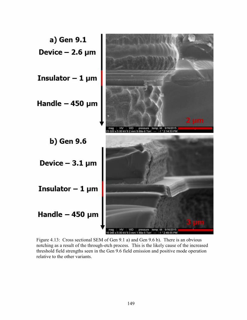
149
Figure 4.13: Cross sectional SEM of Gen 9.1 a) and Gen 9.6 b). There is an obvious
notching as a result of the through-etch process. This is the likely cause of the increased
threshold field strengths seen in the Gen 9.6 field emission and positive mode operation
relative to the other variants.

150
Figure 4.14: a) Field emission signal () as a function of a gating potential at 1 Torr for a
Gen 9.5 microionizer. The electrons obtain 85 eV from the microionizer and interactions
with the buffer gas decrease it. Eventually, near -75 V on the gate, electrons do not have
sufficient energy to generate signal at the detector. b) Average current draws versus field
emission pulse voltage as measured for representative devices from Gen 9.1 (), 9.3 (), 9.5
(), and 9.6 (). The pulse duration is 1 ms and duty cycle is 4.2%. The points are
connected to aid viewing (dashed lines).
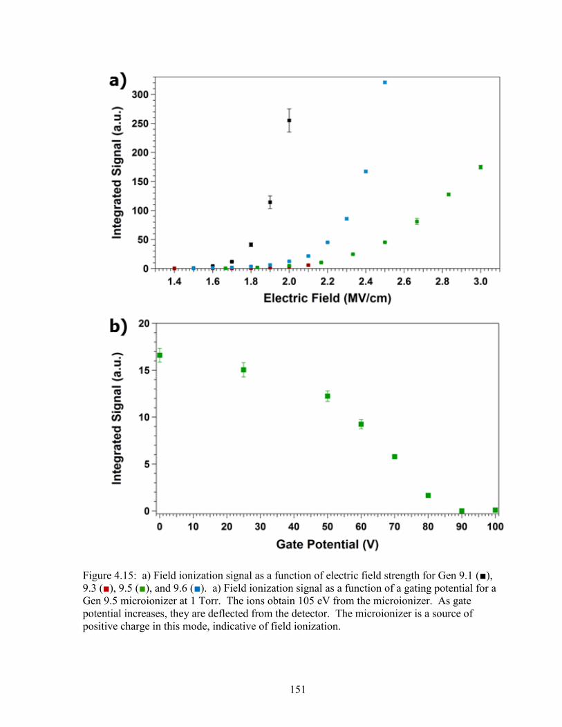
151
Figure 4.15: a) Field ionization signal as a function of electric field strength for Gen 9.1 (),
9.3 (), 9.5 ( ), and 9.6 (). a) Field ionization signal as a function of a gating potential for a
Gen 9.5 microionizer at 1 Torr. The ions obtain 105 eV from the microionizer. As gate
potential increases, they are deflected from the detector. The microionizer is a source of
positive charge in this mode, indicative of field ionization.

152
4.7 REFERENCES
1. Chiu, F. C., A Review on Conduction Mechanisms in Dielectric Films. Adv Mater Sci
Eng 2014.
2. DiMaria, D. J.; Stathis, J. H., Ultimate limit for defect generation in ultra-thin silicon
dioxide. Appl. Phys. Lett. 1997, 71 (22), 3230-3232.
3. Osburn, C. M.; Weitzman, E. J., Electrical-Conduction and Dielectric Breakdown in
Silicon Dioxide Films on Silicon. Journal of the Electrochemical Society 1972, 119
(5), 603-609.
4. Demey, G.; Dewilde, W., Influence of Mobile Ions on Electronic Conduction in
Silicon-Oxide Films. Thin Solid Films 1974, 23 (3), 301-304.
5. Laermer, F.; Schilp, A., Method of anisotropically etching silicon. Google Patents:
1996.
6. Madou, M. J., Fundamentals of microfabrication and nanotechnology. 3rd ed.; CRC
Press: Boca Raton, FL, 2012.
7. Taur, Y.; Ning, T. H., Fundamentals of modern VLSI devices. 2nd ed.; Cambridge
University Press: Cambridge, UK ; New York, 2009; p 656.
8. Fomani, A. A., et al., Low-Voltage Field Ionization of Gases Up to Torr-Level
Pressures Using Massive Arrays of Self-Aligned Gated Nanoscale Tips. Ieee
Transactions on Electron Devices 2014, 61 (5), 1520-1528.
9. Cruz, D., et al., Field emission characteristics of a tungsten microelectromechanical
system device. Appl. Phys. Lett. 2005, 86 (15), 153502.
10. Blakeman, K. H., et al., High-Pressure Mass Spectrometry at Pressures Exceeding 1
Torr in a Microscale Cylindrical Ion Trap. Manuscript in preparation 2015.
11. Schultze, K. P. Advanced System Components for the Development of a Handheld
Ion Trap Mass Spectrometer. Dissertation, University of North Carolina at Chapel
Hill, Chapel Hill, NC, 2014.
153
12. Stuart, M., Conduction in Silicon Oxide Films. Brit J Appl Phys 1967, 18 (11), 1637-
1640.
13. Your Guide to SEMI Specifications for Si Wafers.
http://www.virginiasemi.com/pdf/semi%20specificationsoverview71002.pdf
(accessed 10/8/2015).
14. Fowler, R. H.; Nordheim, L., Electron Emission in Intense Electric Fields.
Proceedings of the Royal Society A: Mathematical, Physical and Engineering
Sciences 1928, 119 (781), 173-181.
15. Allen, F. G.; Gobeli, G. W., Work Function, Photoelectric Threshold, and Surface
States of Atomically Clean Silicon. Physical review 1962, 127 (1), 150-158.
16. van Gorkom, G. G. P.; Hoeberechts, A. M. E., Performance of silicon cold cathodes.
Journal of Vacuum Science and Technology B 1986, 4, 108-111.
17. Whaley, D. R., et al., 100 W Operation of a Cold Cathode TWT. Ieee Transactions on
Electron Devices 2009, 56 (5), 896-905.
18. Schroder, D. K., et al., Semiconductor Field-Emission Photocathode. Ieee
Transactions on Electron Devices 1974, Ed21 (12), 785-798.
19. Baskin, L. M., et al., General Features of Field Emission from Semiconductors. Phys
Status Solidi B 1971, 47 (1), 49-62.
20. Celler, G. K.; Cristoloveanu, S., Frontiers of silicon-on-insulator. J Appl Phys 2003,
93 (9), 4955-4978.
21. Lau, S. P., et al., Changes in the Poole-Frenkel coefficient with current induced defect
band conductivity of hydrogenated amorphous silicon nitride. J Non-Cryst Solids
1998, 227, 533-537.
22. Harrell, W. R.; Frey, J., Observation of Poole-Frenkel effect saturation in SiO2 and
other insulating films. Thin Solid Films 1999, 352 (1-2), 195-204.

154
23. Osburn, C. M.; Ormond, D. W., Dielectric Breakdown in Silicon Dioxide Films on
Silicon: II Influence of Processing and Materials. Journal of the Electrochemical
Society 1972, 119 (5), 597-603.
24. Swaroop, B.; Schaffer, P. S., Conduction in Silicon Nitride and Silicon Nitride-Oxide
Films. J Phys D Appl Phys 1970, 3 (5), 803-806.
25. Yota, J. In Effects of Deposition Method of PECVD Silicon Nitride as MIM Capacitor
Dielectric for GaAs HBT Technology, Electrochemical Society Meeting, Montreal,
Canada, Montreal, Canada, 2011.
26. Blakeman, K. H. Development of High Pressure Mass Spectrometry for Handheld
Instruments. Dissertation, University of North Carolina at Chapel Hill, Chapel Hill,
NC, 2015.
27. Mark, T. D.; Dunn, G. H., Electron impact ionization. Springer-Verlag: Wien ; New
York, 1985; p 383.
28. Wu, B. Q., et al., High aspect ratio silicon etch: A review. J Appl Phys 2010, 108 (5).
29. Jansen, H. V., et al., Black silicon method X: a review on high speed and selective
plasma etching of silicon with profile control: an in-depth comparison between Bosch
and cryostat DRIE processes as a roadmap to next generation equipment. Journal of
Micromechanics and Microengineering 2009, 19 (3).
30. Talin, A. A., et al., Field emission displays: a critical review. Solid-State Electronics
2001, 45 (6), 963-976.
31. Xu, N. S.; Huq, S. E., Novel cold cathode materials and applications. Mat Sci Eng R
2005, 48 (2-5), 47-189.
32. Harman, G. G.; Harman, G. G., Wire bonding in microelectronics. 3rd ed.; McGraw-
Hill: New York, 2010; p 426.
33. Rhoderick, E. H., Metal-semiconductor contacts. Clarendon Press: Oxford, 1978; p
201.

155
34. Lum, I., et al., Footprint study of ultrasonic wedge-bonding with aluminum wire on
copper substrate. J Electron Mater 2006, 35 (3), 433-442.
35. Poate, J. M., et al., Thin-Film Interdiffusion .1. Au-Pd, Pd-Au, Ti-Pd, Ti-Au, Ti-Pd-
Au, and Ti-Au-Pd. J Appl Phys 1975, 46 (10), 4275-4283.
36. Morita, M., et al., Growth of Native Oxide on a Silicon Surface. J Appl Phys 1990, 68
(3), 1272-1281.
37. Gomer, R., Field emission and field ionization. Harvard University Press: Cambridge,
1961; p 195.
38. Zhu, W., et al., Electron field emission from chemical vapor deposited diamond. J
Vac Sci Technol B 1996, 14 (3), 2011-2019.
39. Vangelde.W; Hauser, V. E., Etching of Silicon Nitride in Phosphoric Acid with
Silicon Dioxide as a Mask. Journal of the Electrochemical Society 1967, 114 (8),
869-872.
40. Pillai, A. S.; Hackam, R., Surface Flashover of Solid Insulators in Atmospheric Air
and in Vacuum. J Appl Phys 1985, 58 (1), 146-153.
41. Ono, T., et al., Micro-discharge and electric breakdown in a micro-gap. Journal of
Micromechanics and Microengineering 2000, 10, 445-451.
42. Miller, H. C., Surface Flashover of Insulators. IEEE T Electr Insul 1989, 24 (5), 765-
786.
43. Heinen, H. J., et al., Appearance Potentials of Field Ions. Z Naturforsch A 1974, A 29
(5), 773-781.
44. Au, F. C. K., et al., Electron field emission from silicon nanowires. Appl. Phys. Lett.
1999, 75 (12), 1700-1702.
45. Haynes, W. M., Handbook of Chemistry and Physics. 95th ed.; CRC Press: 2014; p
2693.

156
46. Beckey, H. D., et al., Über die Feldstärkeabhängigkeit der Winkelverteilung
feldemittierter Elektronen und Ionen. In Zeitschrift für Naturforschung A, 1966; Vol.
21, p 141.
47. Beckey, H. D., Principles of field ionization and field desorption mass spectrometry.
1st ed.; Pergamon Press: Oxford Eng. ; New York, 1977; p 335.
48. Rao, K. A., et al., A Combination Electron-Ion Field-Emission Source. J Vac Sci
Technol B 1989, 7 (6), 1793-1797.

157
CHAPTER 5: MICROIONIZER-BASED HIGH PRESSURE MASS
SPECTROMETRY
5.1 Introduction
The first generation microionizer proved capable of field emission mass spectra in high
pressure helium and air (Chapter 3). However, the high power consumption, device-to-
device reproducibility, and lifetime limitations posed serious obstacles for a reliable, portable
HPMS ionization source. Chapter 4 documented the advances made in fabrication and
operation to overcome these obstacles. These advances culminated in the 9th
generation
microionizer, which was shown capable of low-power, field emission and positive mode
operation. This chapter will focus on applying the 9th
generation (Gen 9) as the ionization
source for HPMS.
While microionizer performance improved with advances in design and operation from
the first generation, the realm of high pressure mass spectrometry also advanced. Some of
this advancement was documented in Chapter 4 – mainly with the switch from a
differentially pumped chamber to a miniature chamber.1 This change proved effective in
reducing gas loads and also simplifies ion trap installation, which helped pinpoint sources of
RF discharge, increasing the uptime of the HPMS instruments. Moreover, it significantly
reduces the capacitance of the drive RF electrical feedthrough enabling high frequency
characterization of ion traps with smaller critical dimensions. Evidence suggests that smaller
traps, 100 < r0 < 500 μm, driven at increased RF drive frequencies, f > 6 MHz, aids in
trapping and retention of ions as well as increasing resolution relative to our standard r0 =

158
500 μm traps.2 In addition to the instrument updates, the mass analyzer was upgraded from a
standard CIT to a stretched length ion trap (SLIT).1 The SLIT trap operates identically to a
CIT, only it has an expanded charge capacity relative to a CIT.3 While these HPMS
advances were not vital to the success of the microionizer as a charge source, they were key
to applying the microionizer as an HPMS ion source.
As stated in Chapter 4, Gen 9 microionizers deviated from the symmetric die layout of
the prior generations and corresponded with use of the mini-chamber HPMS. The mini-
chamber is limited to compact ion trap electrodes only (see Chapter 4), which reduces the
area available for aligning the microionizer’s active features with the ion trap. Thus,
alignment is critical for maximizing the signal intensity as either an electron source or ion
source. It was shown in Chapter 2 that external ion trapping for HPMS is mainly a function
of pressure and ion kinetic energy. Combining this experience with that from electrospray
ionization4 show external ion trapping is a balance between ensuring an ion has enough
energy to enter the ion trap but not so much that it cannot be captured by the electric field. In
order to maximize the microionizer’s signal intensity, particularly in positive ion mode, it
needs to be placed in close proximity to the ion trap. By trap-mounting the microionizer, the
separation distance between ionizer and trap is controllable on the order of the mean free
path length (100 μm at 1 Torr). This proximal mounting is important because the collisions
that induce scattering loss outside the trap are crucial to successfully trapping an externally
generated ion once inside the trap.
Four 9th
gen microionizers (9.1, 9.3, 9.5, and 9.6) have successfully operated at high
pressure as both air-based field emission and positive ion mode ionizers. These ionizers are
further characterized for their ability to generate mass spectra under HPMS conditions. Of

159
the four, two (Gen 9.1 and 9.5) will be discussed here. The former was based upon Ultrasil
SOI, with a 3 μm device layer and a 1 μm insulating layer, while the latter had a device layer
of 0.25 μm titanium/chrome and a 0.3 μm insulating layer – both were single-side etched. Of
the remaining variants, Gen 9.3 did not generate sufficient signal intensity (in either field
emission or positive mode) for consistent HPMS operation. Gen 9.6 is a through-etched
version of Gen 9.1, designed to be an atmospheric inlet to the mass spectrometer. In trap-
mounted configuration, it operates similarly to Gen 9.1, but as an atmospheric interface it
serves better as a vision into future microionizer work and as such will be discussed in
Chapter 6. Mass spectral characterization of the two 9th
generation microionizers drew upon
all of the advances made in both microionizer and high pressure mass spectrometry
development - from hardware to operation - in order to examine the ionizer’s behavior under
both field emission and positive ion mode.
5.2 Experimental
The 9th
generation devices were tested in a trap-mounted configuration with a cross-
sectional schematic of the mounted trap shown in Figure 5.1. The PCB-mounted
microionizer was separated from the endcap by 200 or 400 μm Teflon spacers. It was
secured in-place with the same screws and alignment pins (not shown) used to align and
mount the ion trap. Figure 5.2a shows a rendering of a sample inlet plate, mass analyzer
chamber and detection chamber designed to fit the entire PCB-microionizer-trap assembly
into a compact vacuum system. The mass analyzer chamber was an adaptation of the mini-
chamber HPMS,1 designed to fit the entire ionizer-trap assembly inside the vacuum. Figure
5.2b shows an image of the assembly inside the compact system with the sample inlet plate
removed.

160
The ion traps employed for these studies were two SLITs: full-size and half-size. The
full-size SLIT had critical dimensions x0 = 500 μm, y0 = 4.0 mm, and z0 = 645 μm, while the
half-size SLIT had x0 = 250 μm, y0 = 4.0 mm, and z0 = 320 μm. Two types of endcaps were
used: mesh endcaps with 250 lpi spacing and aperture endcaps with x0 = 100 μm. All trap
electrodes were electrochemically etched beryllium copper (Towne Labs). The full-size
SLIT was operated near 9 MHz (± 0.5 MHz), and the half-size SLIT was driven at near
20 MHz (± 0.5 MHz). Operation of the SLIT for HPMS is identical as for the CIT as
previously described.
Three methods of analyte introduction were used. The UHV leak valve and atmospheric
sampling methods were previously described. The third method utilized Tedlar sampling
bags (10 L w/septum, Fisher Scientific). These gas-sampling bags were used in order to
introduce known concentrations of gas to the mass spectrometer. The bags were filled,
heated, and purged three times with nitrogen to reduce trace contaminants.5 Bags were filled
to capacity with nitrogen or air (UHP, National Welders), then heated to about 70 oC with a
heat gun, and the gas was expelled. The bag was then filled just above capacity with buffer
gas and allowed to equalize to room pressure. A syringe and septum were used to introduce
volatile, liquid analytes. Concentrations were calculated by volume in parts per million
(ppm). The analytes included benzene, toluene, o-xylene, p-xylene, mesitylene, aniline,
methylaniline, and dimethylaniline (Sigma-Aldrich, Milwaukee, WI). Trap chamber
pressure was maintained near 1.0 Torr by metering flow rate with a needle valve.
The 9th
generation microionizer was employed as both field emission-based EI and
positive mode ion source. They were mechanically secured to the PCB with epoxy and wire
bonded for electrical contact. Charge production from the microionizer was electrically

161
gated with a voltage pulse (Vp) placed on the handle layer (farthest from trap) of the
microionizer. An additional bias potential (Vb) was continuously applied to aid in control of
the electrons or ions. Previous characterization showed that electron and ion energy are
equal to the total potential during generation: bias + pulse voltages. The pulse and bias were
ballasted with 0.1 to 1 MΩ, 1/2 W resistors. Power supplies for the pulse and bias were high
voltage (Series 230, Bertan-Spellman) and moderate voltage (E3612A, Agilent) models.
Pulse polarity was negative for field emission mode and positive for field ionization mode
and ranged from -300 V to +300 V. Typical field strengths for field emission were near
0.8 MV/cm and for field ionization mode near 2.0 MV/cm. A 4.5 digit multimeter (U1272A,
Agilent) was placed in series with the voltage pulse and operated in DC, μA mode to monitor
the current. The reading varied due to duty cycle, thus the maximum value observed over a
three second visual window was recorded as the average value. This method of measurement
was checked by measuring the voltage across a series resistor (R = 10 kΩ) using an
oscilloscope and found to be within close agreement. Peak current was back calculated by
dividing by the duty cycle of the pulse. Average and peak powers were calculated by taking
the product of the appropriate current and the voltage pulse.
Instrument and data acquisition under LabVIEW control has been described previously.
For the HPMS studies, mass spectra were recorded at 500 kHz acquisition rate for at least
250 averaging and then low pass filtered at 30 kHz. Mass axis calibration was performed
with a LabVIEW program and based upon NIST EI standards. For lifetime studies, file size
became a consideration; therefore signal averaging was increased to 1000 and data
acquisition rate was slowed to 250 kHz. Data was processed with a LabVIEW program,
(SignalIntegrator_v4.vi). The time axis (abscissa) was constructed from the timestamp of

162
each averaged spectrum. MS signal was low pass filtered at 30 kHz and baseline subtracted
assuming a linear offset. The signal-to-noise ratio (SNR) was calculated using the maximum
signal intensity divided by the root mean square noise value calculated between two user-
controlled cursors. Integration of the signal during the ionization pulse and RF ramp portions
of the scan was also performed. Due to the use of an EMT detector, negative charge was not
directly measured. For field emission mode, the integrated ionization pulse was considered
to be directly proportional to the electron emission intensity.
5.3 Results and Discussion
The microionizer was evaluated at 1 Torr air buffer gas in both field emission-based EI as
well as positive ion source mode. Each mode successfully generated mass spectra but with
differing operating characteristics, particularly in regards to emission stability and lifetime.
As such, the results for each mode are discussed separately.
5.3.1 Field Emission HPMS Characterization
Chapter 3 documented mass spectral results with the Gen 1 microionizer operating as a
field emission source in high pressure helium and air buffer gases – though with power draws
on the order of watts and at low duty cycles (less than 2%). Before fully characterizing the
Gen 9 devices, the ability to achieve HPMS with field emission and air buffer gas was
undertaken. Figure 5.3 shows a mass spectrum of o-xylene, sampled via the atmospheric
inlet, where a sample vial was held at the needle valve inlet to the mass spectrometer for
1-2 s. The valve was throttled to 1.0 Torr of room air. This spectrum was taken with a full-
size SLIT at 8.84 MHz. The Gen 9.1 microionizer was trap mounted and spaced 200 μm
from the trap endcap. Field emission was initiated with five, 1 ms pulses of -80 V, yielding a
field strength of 0.8 MV/cm, and a -100 V bias was applied to the ionizer. The average

163
current draw was less than 3 μA, consuming an average of 240 μW. The duty cycle of the
microionizer was 22%, which scales the peak current and power to 13.5 μA and 1.1 mW,
respectively. These power figures represent a decrease of over four orders of magnitude
compared to a thermionic emitter.6 However, they also contrast the Gen 9 microionizer
operation relative to Gen 1. For comparison, Gen 1 microionizers drew a peak of 10 mA of
current (limited by the supply) requiring a low duty cycle of 0.3% to generate field emission
at 0.8 MV/cm. Gen 9 devices accomplished the same role while drawing nearly 400 times
less power. Moreover, because the power draw is low, the duty cycle can be increased. In
this case, the Gen 9 duty cycle is 73 times greater than the Gen 1, meaning there is less dead
time for each mass spectral scan length. This decreased dead time directly impacts the
acquisition rate of the mass spectrometer, which was 12 Hz for Gen 1 and 44 Hz for Gen 9.
The improved acquisition rate is crucial in time sensitive applications such as chemical
warfare agent detection7 as well as when the HPMS is coupled to a rapid separation
techniques such as gas chromatography where higher DAQ rates are needed to accurately
define peaks.1
Generating consistent, predictable mass spectra scan-to-scan is necessary for an
ionization source that will be used in a setting requiring not only detection but quantification;
as a result the source must also present a predictable signal decay in order to compare mass
spectra over time.8 Prior to the 9
th generation, microionizers rarely exceeded more than a few
hours of mass spectral acquisition. Their lifetime was difficult to quantify, because much of
operational time was spent in search for signal intensity, which typically ended in device
over-voltage and shorting before a stable emission point was reached. Inconsistent device-
to-device operation (turn-on voltage, overall emission, discharge threshold) complicated

164
matters further. The 9th
generation overcame the device-to-device inconsistencies through a
combination of wire bonding, ballast resistors, and optimized HPMS operation, opening a
window to measure device lifetimes under conditions that would be seen in a handheld mass
spectrometer application.
Field emission lifetime was evaluated by monitoring the ionization pulse of a Gen 9.1
microionizer. The device was used as a field emission-based EI source for the HPMS and
held at 0.77 Torr (limited by the EMT). A -80 V pulse was applied for 0.9 ms, generating a
0.8 MV/cm electric field biased to -86 V. The duty cycle was 4% (0.9/22.55 ms). The
results of a five-hour field emission lifetime test are shown in Figure 5.4, where each data
point represents the integrated ionization pulse of 500 averaged mass spectra; as such they
are spaced approximately 20 seconds apart. The analyte, o-xylene, was periodically
introduced at the atmospheric inlet to correlate the ionization pulse intensity to a mass
spectral signal strength, as shown in the inset of Figure 5.4. For the first hour, an erratic
signal from point-to-point with an overall decay occurred during the ionization pulse. At 1
hour, signal intensity recovers (with no external intervention) and continues a similar decay
seen in the first hour, only with a slower overall decay rate. At no point during the five hours
does the signal drop to zero, however from the inset showing the mass spectra, it is obvious
the ionization pulse decay negatively impacts the mass spectral performance of the device.
In terms of lifetime, this particular device was operated at various field strengths
(between 0.7 and 1.0 MV/cm) for a total of 9.3 h of instrument time (data not shown). Each
field strength produced a similar pattern – a general decay over the course of hours with
erratic point-to-point reproducibility. At a 4% duty cycle, this corresponds to only 22
minutes of emitter lifetime, but it is spread over 730,000 individual mass spectra. While this

165
lifetime would not be feasible for a portable HPMS operating in a continuous monitoring
mode, it could be used in an instrument that operates on an infrequent basis by spending the
730,000 mass spectra as-needed.
The most concerning feature of Figure 5.4 is the inconsistent nature of the ionization
pulse from point-to-point. Field emission intensity is a strong function of emitter tip
geometry.9 Tip geometry is subject to change over time for two main reasons: ion
bombardment and field desorption.10
Electron impact ionization can occur anywhere along
the electron beam’s path; ions generated within a mean free path length (order of 100 μm at
1 Torr).11
of the emission site will gain energy equivalent to the total potential (pulse plus
bias), which for the data shown in Figure 5.4 was 166 eV. At these energies, ion
bombardment can result in physical sputtering of the tips.12
This sputtering is unpredictable
and can either serve to enhance emission by sharpening the emission site or degrade it by
erosion. Moreover, thermal runaway at the sharpened tips is a concern where Joule heating
promotes electrons into the conduction band, leading to further field emission and higher
intensities. This process, however can feedback until temperatures are sufficient for the tip to
desorb, destroying the emission site and can occur over the nanosecond to microsecond
timeframe.10
Given the 0.9 ms pulse duration of the microionizer, thermal runaway could
account for both the erratic signal from random activation of emission sites and signal decay
from reductions in emission sites across the device. Conversely, working at high pressure
may have increased the ionizer’s lifetime by slowing ions formed in the vicinity of the
ionizer. Most field emission sources operate at pressures below 10-6
Torr, where the mean
free path length is greater than 10 mm. Thus, an ion will experience little or no collisional
cooling and impact with the surface will likely yield sputtering damage. However, at 1 Torr,

166
ions must be generated within 100 μm to avoid collisional cooling. Given the mean free path
for electrons is 2.5 mm13
at this pressure, the rate of ion generation within the 100 μm
threshold is low. But, even a low probability event when spread across the entire
microionizer could be enough to cause erratic signal intensity.
As higher field strengths should lead to improved performance, the microionizer was
operated at a field strength of 1.0 MV/cm (data not shown). After 35 min of operation, the
device suffered insulator breakdown that proved consistent with other tested microionizers.
The breakdown consisted of several bursts of significant instantaneous signal intensity (100
to 1000 times typical signal level) followed by a short circuit across the insulating layer.
Depending upon preparation, silicon dioxide thin films should breakdown near 11 ± 2
MV/cm.14
The observed field strength at breakdown was only 1.0 MV/cm. This
discrepancy was attributed to surface flashover at the vacuum-insulator interface.15-16
The ability to generate mass spectra for an extended time period is paramount for an ion
source. Field emission devices, particularly for display technologies have 10,000+ hour
lifetimes, defined as the time-to-half emission intensity, however these devices require
pristine vacuum environments to achieve these lifetimes.17-18
Field emission mode with the
Gen 9 microionizers generated HPMS with impressive lifetimes with low power
consumption at 1 Torr of air.19
However, the utility of the microionizer in field emission
mode is ultimately limited by two factors: the inconsistent scan-to-scan signal and the
overall signal decay.
5.3.2 Field Ionization HPMS Characterization
The 9th
generation delivered low-power field emission-based mass spectrometry in a high
pressure air environment. While this was encouraging, the inconsistency of the signal
167
intensity limits its use in potential analytical applications so its use as a field ionization
source was explored. Previous attempts at field ionization with Gen 1 through 8 produced
device failure before ionization was detected. This was attributed to insulator breakdown due
to thermal contributions from the leakage current.20
Having reduced the leakage current by
four orders of magnitude, positive mode operation was demonstrated with the Gen 9
microionizer using a gate aperture discussed in Chapter 4. It was shown in Chapter 2 that
external ion injection into the ion trap at high pressure is a balancing act. The ion must have
enough energy to transit from the source-to-trap without scattering, however with not so
much energy that collisional cooling cannot reduce its energy below the potential well depth
of the ion trap. Experimentally, ion injection is dependent upon the ion kinetic energy as
well as the buffer gas pressure. In addition, the high pressures involved in HPMS provide a
wide window of acceptable kinetic energies for successful ion injection.
The experience gained from external ion injection experiments was utilized to couple the
microionizer in positive mode with the HPMS to generate mass spectra. A Gen 9.5
microionizer (300 nm insulating layer) was mounted 400 μm from a full-size SLIT trap. The
field strength was pulsed at 1.63 MV/cm for 1 ms and biased to +50 V. Mass spectra of
several volatile organic compounds (VOC) introduced at the atmospheric inlet needle valve
are plotted in Figure 5.5. Overall, the signal intensities and fragmentation patterns are very
similar to those seen with the microionizer acting as a field emission source. However, the
scan-to-scan signal fluctuations that were observed in field emission mode are not present
(see lifetime results, Figure 5.10). At this point, the ionization mechanism behind positive
mode was thought to be field ionization but not proved conclusively based on the
experiments performed. The aperture experiments documented in Chapter 4 showed the

168
microionizer is indeed a source of positive charge. However, these experiments could not
discriminate between localized field emission-induced EI and direct field ionization. HPMS
offers a powerful tool to examine the ions generated in positive mode to determine their
origins.
Evidence for distinguishing field emission and positive mode operation includes
comparing the relative intensities of the ionization pulses. A Gen 9.1 microionizer was
operated in field emission (0.91 MV/cm and -150 Vb) mode followed by positive mode
(1.12 MV/cm and 0 Vb) without breaking vacuum. Mesitylene was leaked at a constant rate
for both ionization modes and the signal intensities during the ionization pulse and resulting
mass spectra are plotted in Figure 5.6. The ionization pulses are 3 ms in duration (between t
= 3 and 6 ms), while the mass spectra are also 3 ms in duration (between t = 14.5 and
17.5 ms). The ion kinetic energy was adjusted in positive mode such that the mass spectral
signal intensity was similar to field emission mode. Performance can be compared with
integrated mass spectra and ionization pulse signals. The integrated mass spectrum for field
emission mode is 0.55 V*ms, while for positive mode it is 0.47 V*ms. The corresponding
integrated ionization pulses are 205.35 and 5.87 V*ms, respectively. There is a significant
difference in the charge generation efficiency seen for a field emission mass spectrum vs. a
positive mode spectrum. Field emission mode clearly generated more ions than positive
mode. However, only 0.3% of those ions were trapped and detected versus 8.0% for positive
mode. This is further evidence that field ionization is the mechanism behind the positive
mode operation. Field ionization has a threshold behavior; i.e. neutrals with too great an
ionization potential will not ionize21
whereas field emission generates electrons for
subsequent electron impact ionization. EI also does not discriminate between buffer gas and

169
analyte(s) as it will ionize both.22
This is an inefficient process at high pressures when one
considers that analyte concentrations range in the ppb to 100 ppm levels and the buffer gas
comprises over 99% of the neutral molecules in a sample. Therefore, the ionization pulse is
mainly comprised of ionized buffer gas in field emission mode, explaining the discrepancy
between the magnitudes of the ionization pulse and mass spectrum. Consequently, field
ionization generates less wasted charge and targets analytes with lower ionization potentials
than the buffer gas.
Targeted field ionization was demonstrated with a mixture of DMA and benzene
introduced at the atmospheric inlet of the HPMS and various microionizer field strengths.
These compounds were chosen because of the large spread between their ionization
potentials, 7.1 (DMA) and 9.2 eV (benzene) respectively and because of their mass range
(molecular ions at 121 and 78 m/z) and lack of interfering fragments. A series of mass
spectra are shown in Figure 5.7 using a Gen 9.5 device where the electric field was increased
from 1.17 to 1.80 MV/cm. A sample container was wafted at the inlet and the pulse voltage
was slowly increased. When the field strength was 1.17 MV/cm, it is below the ionization
threshold of benzene and near that of DMA so only a slight peak was observed at 121 m/z.
As the field strength increased, the DMA peak at 121 m/z increased in intensity. Benzene
(m/z 78) began to ionize as the field strength approached 1.67 MV/cm with a slight peak
evident. By 1.80 MV/cm the field strength exceeded both analytes’ ionization potentials and
both showed SNR > 50. This ionization field strength dependence is further proof this mode
of operation is field ionization. The benzene spectra in Figure 5.7 add an additional piece of
evidence. HPMS of benzene with EI-based ionization sources are typically dominated by a
fragment peak at 63 amu.23
The benzene mass spectrum at 1.80 MV/cm is clearly dominated

170
by the molecular ion peak at 78 amu. The lack of fragmentation suggests that the ionization
mechanism behind positive mode is softer than EI, further supporting field ionization.24
The emission intensity of a field ionization source is directly proportional to the partial
pressure of the analyte. A typical field ionizer is operated in an environment where the
signal intensity is dominated by the analyte such as in high vacuum25
or in a controlled
atmosphere.26
However, HPMS operates in ambient air, where the analyte represents only a
small fraction of a complex mixture of small molecules. Fortunately, the mass spectrometer
offers a tool to gain insight into the microionizer’s field ionization as a function of partial
pressure. A Gen 9.1 microionizer was used in field ionization mode under optimal
conditions with a constant field strength of 2.4 MV/cm and +35 V bias. Mesitylene
concentrations between 520 and 2080 ppm were achieved by leaking saturated air (2600
ppm) into the vacuum chamber from 0.4 to 1.0 Torr, while a second atmospheric inlet was
adjusted to maintain 1.0 Torr total pressure. The SNR of the mesitylene mass spectra
recorded between 520 and 2080 ppm are plotted in Figure 5.8a. The SNR linearly increases
between 500 and 1300 ppm, above which it plateaus. The plateau is most likely due to space
charge limitations in the ion trap. Further insight can be gained by looking at the total
integrated ionization signal, the ion pulse plus mass spectral intensity. This information is
plotted in Figure 5.8b with the total signal increasing linearly by 21% over a 4-fold increase
in mesitylene concentration. Extrapolating a linear fit to 0 ppm mesitylene reveals a y-
intercept at 21.3 au. Assuming this accounts for field ionization of the buffer gas, then the
mesitylene ionization can be determined by subtracting this baseline from the points in
Figure 5.8b. The increase in mesitylene signal is 4.4-fold, which is close to the increase in
mesitylene concentration, demonstrating a linear response to concentration. The mass

171
spectral results in Figure 5.8a did not reveal the presence of an unknown due to the ionized
buffer gas, however the low mass cutoff at this frequency is near 60 m/z, so smaller
constituents are observable during the ionization pulse but not in the mass spectrum.27
Of
the major ambient air components (nitrogen, oxygen, argon, carbon dioxide, and water
vapor), oxygen has the lowest ionization potential at 12.1 eV.28
With oxygen making up
21% of air, if the field strength were sufficient for oxygen ionization, a discharge would
likely be observed thereby setting the maximum high end field strength. This extends the
microionizer’s usable range beyond typical UV ionization sources with 10.6 eV limits.29
Having determined that positive mode operation is in fact field ionization, it was used to
study external ion injection with the SLIT ion trap, specifically the ion kinetic energy (KE)
effect on HPMS performance at 0.5 and 1.0 Torr. A Gen 9.1 device was trap-mounted
125 μm from a full-size SLIT. Mesitylene partial pressure was held constant along with a
field ionization strength of 2.1 MV/cm and ranging the bias from -200 to -12 V (low to high
KE). The ion KE was calculated from the addition of the Vpulse and Vbias and was limited by
electric discharge. The total integrated ionization (ion pulse plus mass spectrum) is plotted in
Figure 5.9a with the integrated mass spectra plotted in Figure 5.9b. In Figure 5.9a, a linear
increase in total ionization intensity is seen for both pressures as ion kinetic energy is
increased. Moreover, the intensities nearly overlap with 0.5 Torr having a slightly higher
signal intensity that diminishes at higher kinetic energies. A hard sphere approximation
determines the mean free path for mesitylene at 1.0 Torr to be 160 μm and 320 μm at
0.5 Torr.30
Since both path lengths are shorter than the spacing between the microionizer and
trap, we expect similar signal intensities for each pressure. However, the mean free path at
1.0 Torr is similar to the ionizer/trap spacing, so losing a small percentage of the ions to

172
scattering collisions is expected. This difference should diminish as the ions gain enough
kinetic energy to overcome the scattering effect due to the buffer gas.
Interestingly, the same scattering mechanism that is responsible for this difference
improves ion trap operation. The integrated mass spectral portions of the total ionization are
plotted in Figure 5.9b. Below 30 eV, signal is essentially zero because ions do not have
sufficient KE to traverse the field between the ionizer and ion trap. As KE increases, mass
spectral signal does as well with a unique optimal energy, 50 and 150 eV at 0.5 and 1.0 Torr,
respectively with the peak signal at 1.0 Torr 3.5-fold greater than the peak observed at
0.5 Torr. Between 30 and 200 eV, the mass spectral intensity at 1 Torr is 40 to 350% greater
than the peak intensity at 0.5 Torr. This data reinforces the conclusions reached in Chapter 2:
external ion injection is dependent upon both pressure and ion KE where it is more effective
at higher pressure because the increased collisional frequency acts to cool the ions into the
ion trap’s potential well depth. This trend was previously observed at the mTorr level with
helium buffer gas in a QITMS.31
Chapter 2 extended these results to miniature CIT’s
operated at 1 Torr buffer gas and this data extends it to SLIT-based mass analyzers.
The last characteristic evaluated for field ionization mode of operation is lifetime. Field
emission mode with the 9th
generation microionizer utilized a short duty cycle to produced
devices with cumulative lifetimes approaching 25 minutes which were used to achieve
HPMS instrument times near 10 h of continuous scanning. Overall, the scan-to-scan stability
in field emission mode was difficult to control and likely contributed to the short lifetime.
This shortened lifetime was attributed to ion bombardment, which is inevitable due to the
negative potentials required to generate and extract negative charge. The results of field
ionization mode lifetime stand in stark contrast. A Gen 9.1 microionizer was trap mounted

173
400 μm from a full-size SLIT with critical dimensions x0 = 500 μm and z0 = 645 μm operated
at 8.86 MHz. The microionizer electric field was 2.06 MV/cm, set by a 10 ms, 206 V pulse.
The device was biased to -100 V for optimal mass spectral signal strength at 1.05 Torr of
ambient air. Mesitylene was leaked at constant partial pressure via UHV leak valve. Mass
spectra were recorded with 1000 scan averaging yielding about 40 seconds between each
spectrum. The instrument operated for nearly 500 h and was monitored in-person during the
day and remotely overnight. The SNR of the nearly 500 h of continuous operation is plotted
in Figure 5.10. The duty cycle was 44.4%, translating to 220 h of cumulative lifetime for the
microionizer. Over the course of the experiment, the average current and power
consumption never exceeded 3 μA and 0.8 mW, respectively. The discontinuities at 240 and
325 h were due to computer errors, where a DAQ hardware restart was required which could
not be performed remotely. There was significant fluctuation in the signal over the course of
the first 10 h of operation with SNR ranging from 50 to 145. Afterwards, the SNR varied in
an envelope of about ±15 units around an average value. At about 10 h, the average SNR
settled near 100 followed by an asymptotic decay. At 50 h, the SNR had decreased to 50,
roughly 50% of its starting value. At the end of the test (t = 500 h), the device was operating
on average at 20% of its original SNR though at no point did the microionizer cease field
ionizing. While the overall lifetime figures may not be as impressive as other field ionization
sources,25
it is important to note that that the microionizer was tested under HPMS
conditions. It operated for nearly 10 days of cumulative ionization at 1 Torr of air buffer gas
with constant analyte introduction under much harsher conditions than most field ionization
sources are tested.26, 32
Moreover, it achieved this lifetime as both a low power and low
voltage field ionizer – meeting the original project goals.

174
5.3.3 Modes of Failure
The cause of failure in field ionization mode also contrasted with field emission failures.
While both modes suffered failures via insulator breakdown, the field strengths were
different. In field ionization mode, breakdown typically manifested above 2.5 MV/cm, with
some devices approaching 3.5 MV/cm; whereas, field emission mode showed signs of
discharge and breakdown near 1.0 MV/cm. This difference was attributed to surface
flashover – where trapped charges at the insulator-vacuum interface facilitate current flow
along the surface. Surface flashover was observed in field emission mode because of charge
enhancement. Ions produced near the surface of the emission tip act to enhance the electric
field,10
which in turn increases field emission intensity, creating a positive feedback which
enhances the conditions for flashover. In field ionization mode, the bias of the microionizer
repels ions from the surface suppressing the conditions for surface flashover.
In terms of extended operation, signal decays for both field emission and field ionization
as observed in Figures 5.4 and 5.10. However, the decay rate for field emission was much
greater than for field ionization. In order to maintain adequate signal intensity with field
emission, the field strength would have to be increased eventually leading to breakdown of
the insulator and microionizer failure. Field ionization decay was much slower and similar to
field emission, the field strength could be increased to maintain signal intensity as well. Also
like the field emission source, it is possible for a device to bump up against the field
breakdown strength (near 2.6 MV/cm) and display zero ionization intensity. The cause of
breakdown was not thought to be due to ion bombardment. The next likely culprit
considered was a thin film barrier preventing neutrals from accessing the field strengths
necessary for ionization. Device recovery was attempted by operating in field emission

175
mode but without success (data not shown). Venting to atmosphere as well as pumping to
low pressure (~10-5
Torr) also failed to recover field ionization as did rinses in mild organic
solvents. Harsh chemical cleanings and etches were not possible due to the exposed wire
bonds. As such the mechanism behind signal decay was undetermined, but is believed to be
a thin film buildup.
5.4 Conclusions
Both field emission and field ionization sources were successfully developed for HPMS
applications. Strong mass spectra were recorded with a field emission microionizer however
signal fluctuations and lifetime issues reduce its efficacy as an ionization source. The longest
lasting field emission device ran for an accumulated 9 h of instrument time – roughly 22
minutes of cumulative ionizer lifetime. After thorough testing, the positive ion mode was
attributed to field ionization. Due to the more favorable electric field polarity and selective
ionization of the analyte, field ionization displayed over a 50-fold increase in lifetime over
field emission mode. The longest lasting device provided 20.6 days of instrument time and
9.1 days of cumulative ionization. Moreover, both modes were shown to operate with
average currents draws on the order of microamps and average power consumption between
0.5 and 5.0 mW, depending upon insulating layer thickness. Overall, the 9th
generation
microionizers accomplished each goal set forth at the beginning of the project under the
specified HPMS conditions for a portable instrument.

176
5.5 Figures
Figure 5.1: Cross sectional schematic of the mini-chamber HPMS with a trap mounted
microionizer. The entire assembly fits into the trap chamber and is held at 1.0 Torr with the
EMT on the Detector-side held a < 100 mTorr. In order to maximize signal, the active
features of the microionizer are laid out to match the length of the SLIT. The microionizer is
aligned and mounted with the same hardware as used to build the SLIT.

177
Figure 5.2: The mini-chamber HPMS adapted to work with the trap-mounted microionizer.
a) Solidworks schematic of the chamber showing the sample inlet, microionizer and detector
placement relative to the SLIT (mass analyzer). b) Image of the assembled vacuum chamber
with the sample inlet plate removed showing the mounted microionizer. The microionizer is
positioned about 400 μm from the SLIT.

178
Figure 5.3: High pressure mass spectrum of o-xylene in field emission mode () and NIST
standard (). The spectrum was taken in room air at 1.0 Torr with a x0 = 500 μm and z0 =
645 μm SLIT operated at 8.84 MHz drive RF. A series of five, 1 ms pulses (with 1 ms
periodicity) were used for ionization. Gain on the current preamplifer was 1 μA/V.

179
Figure 5.4: a) The lifetime of a Gen 9.1 microionizer operated in field emission mode was
investigated by plotting the integrated ionization pulse as a function of time (). Analyte was
introduced at the atmospheric inlet. b)Three of the resulting mass spectra are shown from t =
0 (*), 3.4 (*), and 5.0 (*) hours. The electric field strength was 0.8 MV/cm, generated with a
-80 V pulse applied for 0.9 ms (4% duty cycle). The average current never exceeded 1 μA
for an average power of 80 μW.

180
Figure 5.5: Offset high pressure mass spectra of several VOCs acquired in field ionization
mode: mesitylene (); toluene (); benzene (); and aniline, methylaniline, and
dimethylaniline (). HPMS pressure was 0.93 Torr of room air and the analytes were
introduced by wafting from open containers. The field strength was 1.63 MV/cm, pulsed for
1 ms (4.5% duty cycle), and biased +50 V relative to the trap endcap. The SLIT (x0x0
= 500 μm and z0 = 645 μm) was operated at 8.74 MHz using double resonance at 2.95 MHz.

181
Figure 5.6: Overlay of mass spectra recorded in field emission () and positive mode ()
including both the ionization pulse and mass spectrum for each mode. The spectra were
taken with the same ion trap, analyte concentration, and ion pulse length of 3 ms ionization
pulse. The mass spectra were tuned near the same integrated signal intensity in order to
demonstrate the difference in ionization pulses between the two modes.

182
Figure 5.7: Mass spectra of a dimethylaniline and benzene mixture using field ionization
with increasing field strengths of 1.17 MV/cm (); 1.53 MV/cm (); 1.67 MV/cm ();
and 1.80 MV/cm (), the mass spectra are offset for clarity. Dimethylaniline has a m/z =
121 amu and ionization energy of 7.1 eV and benzene has a m/z = 78 amu and ionization
energy of 9.2 eV.

183
Figure 5.8: a) SNR of mass spectra taken in field ionization mode increasing concentrations
of mesitylene at a constant 1 Torr total pressure. The HPMS response is linear between 520
and 1320 ppm, above which the ion trap appears to saturate. b) Total integrated ion signal
(ion pulse plus MS ramp) for the same experiment, showing a linear response from the
microionizer across the entire pressure range.
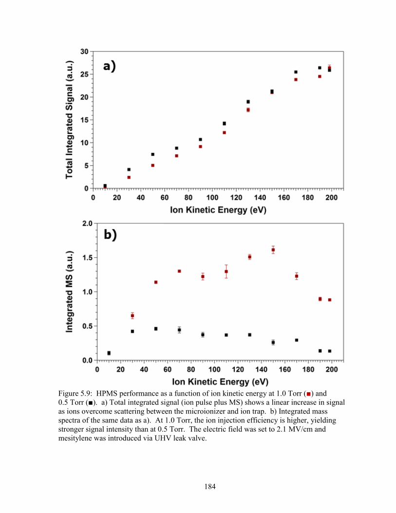
184
Figure 5.9: HPMS performance as a function of ion kinetic energy at 1.0 Torr () and
0.5 Torr (). a) Total integrated signal (ion pulse plus MS) shows a linear increase in signal
as ions overcome scattering between the microionizer and ion trap. b) Integrated mass
spectra of the same data as a). At 1.0 Torr, the ion injection efficiency is higher, yielding
stronger signal intensity than at 0.5 Torr. The electric field was set to 2.1 MV/cm and
mesitylene was introduced via UHV leak valve.

185
Figure 5.10: Signal to noise ratio of a single microionizer operated in field ionization mode.
The Gen 9.1 device was pulsed for 10 ms with constant field strength at 2.06 MV/cm and
biased to -100 V. The duty cycle was 44.4%. The discontinuities in the plot are due to
computer errors which halted acquisition. The ionizer operated for approximately 220 h
when corrected for duty cycle, and 495 h of HPMS total uptime.

186
5.6 REFERENCES
1. Schultze, K. P. Advanced System Components for the Development of a Handheld
Ion Trap Mass Spectrometer. Dissertation, University of North Carolina at Chapel
Hill, Chapel Hill, NC, 2014.
2. Blakeman, K. H.; Ramsey, J. M., High Pressure Mass Spectrometry in Nitrogen and
Air. Manuscript in preparation 2014.
3. Ramsey, J. M.; Schultze, K., Miniature charged particle trap with elongated trapping
region for mass spectrometry. Google Patents: 2014.
4. Gilliland, W. M., et al., Coupling Microchip Electrospray Ionization Devices with
High Pressure Mass Spectrometry. Manuscript in preparation 2015.
5. Miller, S., Personal communication. May 22, 2015.
6. Jenkins, R. O., A Review of Thermionic Cathodes. Vacuum 1969, 19 (8), 353-359.
7. Smith, J. N., et al., Facility monitoring of chemical warfare agent simulants in air
using an automated, field-deployable, miniature mass spectrometer. Rapid Commun.
Mass Spectrom. 2011, 25 (10), 1437-1444.
8. Huq, S. E., et al., Field emitters for space application. J Vac Sci Technol B 2001, 19
(3), 988-991.
9. Fowler, R. H.; Nordheim, L., Electron Emission in Intense Electric Fields.
Proceedings of the Royal Society A: Mathematical, Physical and Engineering
Sciences 1928, 119 (781), 173-181.
10. Fursey, G., Field emission in vacuum microelectronics. Kluwer Academic/Plenum
Publishers: New York, 2005; p 205.
11. Borsdorf, H., et al., Atmospheric-pressure ionization studies and field dependence of
ion mobilities of isomeric hydrocarbons using a miniature differential mobility
spectrometer. Analytica Chimica Acta 2006, 575 (1), 76-88.

187
12. Madou, M. J., Fundamentals of microfabrication and nanotechnology. 3rd ed.; CRC
Press: Boca Raton, FL, 2012.
13. Hoffman, K. R., et al., Total-Cross-Section Measurements for Positrons and Electrons
Colliding with H-2, N-2, and Co2. Physical Review A 1982, 25 (3), 1393-1403.
14. Ainger, F. W., The Formation and Devitrification of Oxides on Silicon. J Mater Sci
1966, 1 (1), 1-13.
15. Pillai, A. S.; Hackam, R., Surface Flashover of Solid Insulators in Atmospheric Air
and in Vacuum. J Appl Phys 1985, 58 (1), 146-153.
16. Miller, H. C., Surface Flashover of Insulators. IEEE T Electr Insul 1989, 24 (5), 765-
786.
17. Wei, Y., et al., Surface chemical changes on field emitter arrays due to device aging.
J Vac Sci Technol B 1999, 17 (1), 233-236.
18. Talin, A. A., et al., Field emission displays: a critical review. Solid-State Electronics
2001, 45 (6), 963-976.
19. Charbonnier, F., Arcing and voltage breakdown in vacuum microelectronics
microwave devices using field emitter arrays: Causes, possible solutions, and recent
progress. J Vac Sci Technol B 1998, 16 (2), 880-887.
20. Osburn, C. M.; Weitzman, E. J., Electrical-Conduction and Dielectric Breakdown in
Silicon Dioxide Films on Silicon. Journal of the Electrochemical Society 1972, 119
(5), 603-609.
21. Gomer, R., Field emission and field ionization. Harvard University Press: Cambridge,
1961; p 195.
22. Mark, T. D.; Dunn, G. H., Electron impact ionization. Springer-Verlag: Wien ; New
York, 1985; p 383.
23. Blakeman, K. H.; Hampton, A. S., Personal Communication. 2015.

188
24. Beckey, H. D., Principles of field ionization and field desorption mass spectrometry.
1st ed.; Pergamon Press: Oxford Eng. ; New York, 1977; p 335.
25. Aberth, W.; Spindt, C. A., Characteristics of a Volcano Field-Ion Quadrupole Mass-
Spectrometer. International Journal of Mass Spectrometry and Ion Processes 1977,
25 (2), 183-198.
26. Fomani, A. A., et al., Low-Voltage Field Ionization of Gases Up to Torr-Level
Pressures Using Massive Arrays of Self-Aligned Gated Nanoscale Tips. Ieee
Transactions on Electron Devices 2014, 61 (5), 1520-1528.
27. Blakeman, K. H., et al., High-Pressure Mass Spectrometry at Pressures Exceeding 1
Torr in a Microscale Cylindrical Ion Trap. Manuscript in preparation 2015.
28. Stein, S. E., "Mass Spectra". in NIST Chemistry WebBook, NIST Standard Reference
Database Number 69 [Online] Linstrom, P. J.; Mallard, W. G., Eds. National Institute
of Standards and Technology, Gaithersbrug, MD, http://webbook.nist.gov, (accessed
10/2/2015).
29. Sielemann, S., et al., IMS with non radioactive ionization sources suitable to detect
chemical warefare agent simulation substances. International Journal of Ion Mobility
Spectrometry 2002, 5 (3), 143-148.
30. Lin, S. N., et al., Dependence of Polyatomic Ion Mobilities on Ionic Size. J Chem
Phys 1974, 60 (12), 4994-4999.
31. Louris, J. N., et al., Injection of Ions into a Quadrupole Ion Trap Mass-Spectrometer.
International Journal of Mass Spectrometry and Ion Processes 1989, 88 (2-3), 97-
111.
32. Johnson, B. B., et al., Field ionization characteristics of an ion source array for
neutron generators. J Appl Phys 2013, 114 (17).
189
CHAPTER 6: CONCLUSIONS AND FUTURE WORK
6.1 Conclusions
The development of the microionizer was undertaken to help develop and advance high
pressure mass spectrometry (HPMS). The ultimate goal is to not only release mass
spectrometry from the confines of the laboratory but also to reduce hardware costs. This
would help make mass spectrometry a ubiquitous technique bringing its chemical informing
power to as many toolboxes as possible. The research presented in this dissertation began in
earnest in 2011. Since then, a low-cost, portable HPMS instrument has been
commercialized1 and used in the field to target volatile organic chemicals.
2 In this sense, the
overall goal of producing a handheld mass spectrometer has been achieved. However,
continued advancement and refinements are necessary to improve the performance of HPMS
in terms of resolution,3 sensitivity,
4 range of detectable analytes,
5 as well as cost-effective
miniaturization.6
The project began with three, simple objectives:
1. Demonstrate HPMS with the microionizer in air.
2. Maximize microionizer lifetime under HPMS conditions.
3. Minimize overall microionizer/mass analyzer footprint.
At the outset of the project, HPMS was in its early stage of development. The tenets of
HPMS – high-pressure, high-frequency, miniature ion trap-based mass spectrometry – had
been shown to work in helium at relatively high pressures (≈ 10 mTorr) of helium.7-8
The
goals of 1 Torr operation in helium,9-10
nitrogen3, and air
11 were achieved using proven
190
internal, electron impact ionization (EI) sources. As an external ion source, the microionizer
was not guaranteed to be compatible with the miniature cylindrical ion trap (mCIT) under
HPMS conditions due to potential well depth concerns of the mCIT relative to a standard
QIT.12-13
Thus, initial studies focused on coupling traditional, external ion sources with the
mCIT under HPMS conditions to determine operational boundaries. Using both off and on-
axis external ion sources, helium, nitrogen, and air were studied from 0.01 to 1.0 Torr. The
trends in the signal intensity of mass spectra revealed several important points: the potential
well depth and small trap dimensions of HPMS are indeed compatible with external ion
injection. External ion trapping was shown to be dependent upon buffer gas composition and
pressure, ion kinetic energy, and ion trap operation. The window of acceptable ion kinetic
energies was widest at 1 Torr of air buffer gas; and under these conditions, it was shown that
deeper well depth also aids external ion trapping. These studies provided operational
boundaries for the microionizer. Deeper well depths, achieved by increasing the drive RF
frequency and amplitude, provide the best opportunity for external ion injection. Buffer gas
composition and pressure are both related to collisional cooling. Larger buffer gases (air or
nitrogen vs. helium) can remove more energy per collision than lighter ones, while pressure
controls the collisional frequency. Ion kinetic energy needs to be high enough to overcome
collisional cooling and scattering between the source and trap, but not so large that the ion
skips through the trap. Most importantly, it was found that increased pressure (1 Torr)
provides the best trapping efficiency. While this must be balanced with ion trap resolution, it
provides a wide range to tune the parameters relative to one another. Thus, source-to-trap
spacing, ion kinetic energy, operational pressure, and RF drive frequency and amplitude can

191
be optimized based upon instrument design constraints as well as analyte properties (m/z,
etc).
Studies of the microionizer began with first generation devices provided via collaboration
with Dr. Pau at the University of Arizona. These devices were successfully coupled with
HPMS and produced internal, EI-based mass spectra in both helium and air at pressures
ranging from a few mTorr to 1 Torr. Field emission was achieved at field strengths below
1 MV/cm, but field ionization was never realized. Although successful in producing spectra,
this generation of microionizer had high-current draw (current limited to 10 mA); a short
lifetime (a few hours of instrument time); and poor field emission stability making it
unsuitable for potential hand held use. These drawbacks were addressed with improvements
in design, materials, fabrication, and operation procedures and culminated in a 9th
generation
microionizer.
The 9th
generation devices utilized every advance in HPMS, fabrication, and microionizer
operation learned throughout the course of this research project. The active features were
designed to align with a stretched length ion trap (SLIT) to maximize signal intensity.4, 6
The
microionizer-to-ion trap spacing was minimized by the use of a printed circuit board (PCB)
based microionizer mount. The result was an ion source capable of mounting within one,
ionic mean free path length (≈ 100 µm) of the ion trap. Optimal electrical contact to the
silicon was achieved by combining metallized contact pads and wire-bonding. The current
draw was reduced from milliamps to microamps yielding, sub-milliwatt average power.
Moreover, both field emission and field ionization modes were possible: electric field
strengths for field emission were less than 1.0 MV/cm while field ionization began near
1.5 MV/cm and was observed upwards of 3.0 MV/cm. A study of several variants using

192
different materials and geometries were compared using current draw, emission currents
(both electron and ion), mass spectra, and lifetimes as the criteria. Two variants, bonded
silicon-on-insulator (SOI) and metal-on-insulator substrates were the best performers. Both
yielded emission currents (electron and ion) as well as mass spectra at 1 Torr of air buffer
gas, with the longest observed lifetime to be over 20 days of HPMS instrument time for the
SOI-based variant. Fabrication yield and HPMS performance showed SOI to be the better
material, but metal-on-insulator is a lower-cost alternative and could be worth additional
investigation.
The data gathered with the 9th
generation microionizer brought the project around full-
circle. Not only did the microionizer corroborate the initial conclusions regarding external
ion injection under HPMS conditions; but in doing so, all three of the major objectives: air-
based HPMS; maximum lifetime; and minimum footprint were achieved.
6.2 Future Work
While the microionizer has successfully demonstrated HPMS operation, there are several
aspects including signal intensity, operational voltage, field emission mode and signal loss
over time that could be addressed to improve on its strengths. In comparison to glow
discharge, the microionizer displays both reduced power consumption and mass spectral
signal intensity by about two orders of magnitude.11
The microionizer does have a smaller
footprint and hence a reduction in pumping capacity required for the smaller volume relative
to the GD. However, the lower sensitivity may not be worth the power gains in a portable
instrument designed for rapid chemical detection.14
Improvement in sensitivity is an area in
need of future research with three possible design changes that could improve sensitivity
worth investigating: 1) use the microionizer as the atmospheric inlet of the MS; 2) combine

193
the microionizer and endcap of the ion trap; 3) further reduce the insulating layer thickness
for reduced voltage operation.
6.2.1 Microionizer as Atmospheric Inlet
Many field ionization sources force the gas flow through their high field regions resulting
in near 100% ionization of neutral analytes.15-17
Combining this efficiency with the
improved trapping of externally injected ions at 1 Torr (as demonstrated in Chapter 2) could
increase signal intensity generated by the microionizer.
Preliminary studies using the microionizer as an atmospheric inlet were attempted where
the gas flow was forced through the active regions of a Gen 9.6 microionizer. Figure 5.2a
shows a cross-sectional diagram of the atmospheric inlet version of the mini-chamber and
Figure 6.1b shows the microionizer mounted to the coverplate of the mass analyzer chamber.
In this configuration, the microionizer was sealed to the PCB with epoxy ensuring all gas
flow into the chamber passed through the high-field region of the microionizer. This
configuration moved the microionizer away from the ion trap so a tube lens was incorporated
to ensure maximum ion transmission into the ion trap.5 The tube lens, 5 mm in length and
5 mm in diameter, was mounted on top of the ion trap endcap and spaced 140 μm from the
endcap using a Teflon spacer. The focusing field was generated by a DC potential ranging
from -135 to +135 V.
Pressure measurements on either side of the microionizer (14.6 Torr inlet side and 1 Torr
outlet side) suggest the microionizer was indeed acting to limit conductance into the ion trap
chamber. With the gas flow forced through the high-field region, both field emission and
field ionization modes were tested. Field emission proved to be unstable, resulting in
uncontrollable discharges. Field ionization mode with mesitylene as the test analyte

194
performed slightly better, generating mass spectra for nearly 1 hour of instrument time. A
steady stream of field ionization was present, but it was generally masked by random
discharges, similar to (but less frequent) than those observed in field emission mode. The
discharges point towards the need to investigate thinner insulating layers as this would lower
the voltages needed to create sufficient field strengths. The field strength for these
experiments was near 3.0 MV/cm, requiring a 300 V pulse voltage, which approaches
Paschen breakdown under these conditions.18
While these preliminary studies showed
limited success for the microionizer as an atmospheric inlet, the fact that any mass spectra
under these conditions were produced is an encouraging first step down this path. Further
pursuit is warranted, because of the possible gains in sensitivity. As the atmospheric inlet,
virtually all of the analyte sampled from the air can be ionized and efficient ion injection at
high pressure will ensure the analyte ions are retained. This would lead to either more signal
at the existing atmospheric sampling flow rate, or the ability to reduce the flow rate and
vacuum pump power consumption.
6.2.2 Microionizer as Ion Trap Endcap
A second method for potentially improving the sensitivity is to substitute the
microionizer for one (or both) of the mCIT endcap(s). With this configuration, gas flow is
forced through the microionizer/endcap (similar to the atmospheric inlet) with the ions
exiting the microionizer directly into the ion trap. Because of the short travel distance (≤ 250
m) between microionizer and trap, ion transmission losses should be minimized thereby
maximizing sensitivity. Note the insulating layer thickness would need to be chosen such that
the potential required for field ionization does not produce ions with too much kinetic energy
for injection.

195
Additionally, this arrangement could reduce the vacuum volume and thus pumping
requirements. The ‘trap chamber’ could consist of the internal volume of the mCIT which
would reduce overall power consumption of the vacuum system. Finally, it could be used in
tandem with an ambient source such as ESI with the ions sprayed through the
microionizer/endcap into the ion trap. The same ion trap assembly could be used to sample
both highly volatile compounds via atmospheric sampling or thermal desorption as well as
less volatile compounds via ambient techniques.
6.2.3 Further Microionizer Development
Early development of the microionizer was plagued by high leakage current, which was
combated with SOI wafers containing thick insulating layers (≈ 1 µm). Improvements in
fabrication and wire bonding reduced the leakage current, and it is likely that SOI substrates
with thinner insulating layers could be used. Insulating layers as thin as 300 nm in SOI-
alternatives were able to generate field ionization with potentials near 50 V; about one-third
the applied potential required for field ionization with thick, 1 µm insulators. Further
thinning of the insulating layer could drop the potentials for field emission and field
ionization even further, which would simplify the pulsing circuity necessary for ionizer
operation and reduce the risk of arc discharge. The latter benefit would also align very well
in efforts to use the microionizer as an atmospheric inlet.
Decreasing the insulator thickness should offer better lifetime – both for field emission
mode as well as field ionization signal intensity vs. time. Both modes showed a general
decrease in signal intensity over time, with field emission mode decaying much faster than
field ionization mode. For field emission mode, this was attributed to emitter tip erosion due
to ion back streaming. For field ionization mode, the decay in signal intensity is most likely

196
the result of adsorbed neutrals on the microionizer. By reducing insulator thickness, field
emission could be achieved with smaller potentials (e.g. 10 V or less). This would reduce the
maximum possible kinetic energy of stray ions and limit damage due to back streaming. The
end result would be a smooth, predictable field emission current. Moreover, short pulses of
field emission mode can be used to clear the adsorbed layer off of the surface of field
ionizers.19
Thus, periodic field emission mode pulses or even alternating field emission and
field ionization MS scans could reduce the rate of signal decay for field ionization mode –
potentially increasing lifetime.
6.3 Applications Beyond HPMS
More traditional field effect devices rely upon Spindt cathodes (or similar geometries)
and tend to require rather complicated fabrication processes.20-21
The strength of the
microionizer is its simple design and fabrication.22
This should translate to lower costs upon
scaling up fabrication. As such, the microionizer might find use beyond HPMS. Thus, it
could prove to be a low cost alternative to other field effect devices that have been developed
for applications ranging from RF amplifiers23
to field effect transistors24
and even
microsatellite ion thrusters.25
These applications would be best approached via
collaborations, where proof of concept experiments could be achieved by tailoring the PCB
mount to each application. Further development could then utilize more advanced designs
similar to that proposed for the endcap-based microionizer.

197
6.4 Figures
Figure 6.1: Solidworks schematic and images of the atmospheric inlet mini-chamber and
coverplate. a) Cross-sectional view of the mini-chamber which highlights the inlet,
microionizer, tube lens, and SLIT positions. b) An image of a microionizer mounted in
coverplate ready for atmospheric inlet operation; the ionizer is sealed to the PCB with epoxy
and a Viton o-ring (not shown) between the aluminum cover plate and PCB ensures gas flow
through the high-field region.

198
6.5 REFERENCES
1. M908 Spec Sheet. http://908devices.com/wp-content/uploads/2014/10/SpecSheet-
908_2014_v21.pdf (accessed 11/3/2015).
2. Nanos, J., 908 Devices has a hand-held approach to thwarting chemical attacks.
Boston Globe 4/20/2015, 2015.
3. Blakeman, K. H. Development of High Pressure Mass Spectrometry for Handheld
Instruments. Dissertation, University of North Carolina at Chapel Hill, Chapel Hill,
NC, 2015.
4. Ramsey, J. M.; Schultze, K., Miniature charged particle trap with elongated trapping
region for mass spectrometry. Google Patents: 2014.
5. Gilliland, W. M., et al., Coupling Microchip Electrospray Ionization Devices with
High Pressure Mass Spectrometry. Manuscript in preparation 2015.
6. Schultze, K. P. Advanced System Components for the Development of a Handheld
Ion Trap Mass Spectrometer. Dissertation, University of North Carolina at Chapel
Hill, Chapel Hill, NC, 2014.
7. Goeringer, D. E., et al., Theory of high-resolution mass spectrometry achieved via
resonance ejection in the quadrupole ion trap. Analytical chemistry 1992, 64 (13),
1434-1439.
8. Kornienko, O., et al., Micro ion trap mass spectrometry. Rapid Commun. Mass
Spectrom. 1999, 13 (1), 50-53.
9. Blakeman, K. H., et al., High-Pressure Mass Spectrometry at Pressures Exceeding 1
Torr in a Microscale Cylindrical Ion Trap. Manuscript in preparation 2015.
10. Wolfe, D. W. High-Pressure Cylindrical Ion Trap Mass Spectrometry. Dissertation,
University of North Carolina, Chapel Hill, 2012.
11. Blakeman, K. H.; Ramsey, J. M., High Pressure Mass Spectrometry in Nitrogen and
Air. Manuscript in preparation 2014.

199
12. McLuckey, S. A., et al., Ion Trap Mass Spectrometry of Externally Generated Ions.
Analytical chemistry 1994, 66 (13), 689-696.
13. March, R. E., An Introduction to Quadrupole Ion Trap Mass Spectrometry. Journal of
Mass Spectrometry 1997, 32 (4), 351-369.
14. Lammert, S. A., Field Portable Mass Spectrometry. In Detection of chemical,
biological, radiological and nuclear agents for the prevention of terrorism : mass
spectrometry and allied topics, Banoub, J., Ed. Springer: New York, 2014; p 291.
15. Aberth, W.; Spindt, C. A., Characteristics of a Volcano Field-Ion Quadrupole Mass-
Spectrometer. International Journal of Mass Spectrometry and Ion Processes 1977,
25 (2), 183-198.
16. Fomani, A. A., et al., Low-Voltage Field Ionization of Gases Up to Torr-Level
Pressures Using Massive Arrays of Self-Aligned Gated Nanoscale Tips. Ieee
Transactions on Electron Devices 2014, 61 (5), 1520-1528.
17. Ghodsian, B., et al., Gas Detector with Low-Cost Micromachined Field Ionization
Tips. IEEE Electron Device Letters 1998, 19 (7), 241-243.
18. Lisovskiy, V. A.; Yakovin, S. D., Experimental study of a low-pressure glow
discharge in air in large-diameter discharge tubes: I. Conditions for the normal regime
of a glow discharge. Plasma Phys Rep+ 2000, 26 (12), 1066-1075.
19. Beckey, H. D., Principles of field ionization and field desorption mass spectrometry.
1st ed.; Pergamon Press: Oxford Eng. ; New York, 1977; p 335.
20. Spindt, C., et al., Thermal field forming of Spindt cathode arrays. J Vac Sci Technol B
2015, 33 (3).
21. Fomani, A. A., et al., Toward Amp-Level Field Emission With Large-Area Arrays of
Pt-Coated Self-Aligned Gated Nanoscale Tips. Ieee Transactions on Electron Devices
2014, 61 (7), 2538-2546.
22. Madou, M. J., Fundamentals of microfabrication and nanotechnology. 3rd ed.; CRC
Press: Boca Raton, FL, 2012.

200
23. Temple, D., Recent progress in field emitter array development for high performance
applications. Mat Sci Eng R 1999, 24 (5), 185-239.
24. Lim, H. J., et al., Impact of the crystallization of the high-k dielectric gate oxide on
the positive bias temperature instability of the n-channel metal-oxide-semiconductor
field emission transistor. Appl. Phys. Lett. 2013, 102 (23).
25. Hartley, F. T., Miniature Free-Space Electrostatic Ion Thrusters. Stephens, J. B., Ed.
NASA: NASA Technology Briefs, 2006; p 29.

201
APPENDIX 1: LIST OF MICROFABRICATION TECHNIQUES, TOOLS, AND
GENERAL RESOURCES
A1.1 Tools and Techniques Used During Fabrication Development
Tool/Technique Purpose Location
Karl Suss MA6/BA6
Photolithography –
Exposure UNC/CHANL
Laurell WS-650 Spin Coater
Photolithography –
Photoresist Application UNC/CHANL
Kurt J Lesker PVD-75
Magnetron Sputter Coater
Thin Metallic Film
Deposition UNC/CHANL
Electron Beam Evaporator
Thin Metallic Film
Deposition UNC/CHANL
Tempress LPCVD Furnace
Si3N4 and Polysilicon
Deposition UA/TMNFC
Cricut Explore Xerography UNC
Furnace Annealing UNC
Alcatel AMS-100 DRIE
Anisotropic Etching and
Plasma Cleaning UNC/CHANL
Trion Mini-lock Phantom III
RIE/ICP
Isotropic Etching and
Plasma Cleaning UNC
AGS RIE Isotropic Etching UA/TMNFC
Trion Phantom II RIE Isotropic Etching Duke/SMIF
SPTS Pegasus Deep Silicon
Etcher Anisotropic Etching Duke/SMIF
Transene Chromium Etch 1020 Chrome Etch UNC
Transene Buffered Oxide Etch Isotropic SiO2 Etching UNC
Heated Phosphoric Acid Si3N4 Etching UNC
Scribe and Break Dicing UNC
Disco-XXX Dicing UNC
WestBond 7KE Wire Bond UNC
Cyantek Nanostrip 2X Cleaning UNC
SC1/SC2 (RCA Series) Cleaning UNC
Table A1.1: List of fabrication tools and techniques employed.

202
A1.2 Notes and Resources
The following information is a list of useful hints, tricks, and resources accumulated
during the development of the process flow for microionizer fabrication. This list is not
meant to be exhaustive but should be a good starting point for future deep, anisotropic
etching with or without SOI substrates.
A1.2.1 General Resources
There are many resources for semiconductor (specifically silicon) theory and fabrication.
This project relied heavily upon Madou’s series on micro and nanofabrication for
introductory information as well as citations for further research.1 The classic book by Sze,
Physics of Semiconductors Devices, was also very useful.2 Several other books were used for
more specific aspects of the project including metal-semiconductor contacts,3 wire bonding,
4
and silicon-on-insulator technology.5 There were also several research articles and reviews
regarding insulating layers that are worth mentioning: conduction in insulators;6-8
silicon
dioxide characteristics and breakdown;9-11
and materials for field emission devices.12
Finally
two articles by Williams, et al were crucial for practical microfabrication. These articles
report the etch rates of many common semiconductors, metals, and polymers under different
etch and cleaning processes.13-14
A1.2.2 Cleaning and Wet Etches
Photoresist removal is best done with oxygen plasma or Nanostrip 2X (Cyantek
Corporation). 150 mm wafers do not fit into either of the oxygen plasma cleaners at UNC;
the DRIE and RIE can substitute but will leave behind resist along the edge. Nanostrip 2X
is a stabilized piranha solution (sulfuric acid + hydrogen peroxide + peroxymonosulfuric
acid), and it is less likely to result in explosive hydrogen outgassing than standard piranha. It

203
is best for removing organics, certain metals, and photoresists. If heated to ≈ 75 oC, it can
even remove stubborn negative resists such as KMPR or SU-8. Heating will significantly
deplete the strength of the solution and it is not recommended to be reused afterwards.
The SC1/SC2 cleaning series, developed by Kern at RCA, should be used whenever the
surface of the substrate needs to be pristine.15-16
Examples of when it would be appropriate
are to prep a wafer that is no longer ‘prime’ for spin coating (e.g. double-sided processing) or
for a thin film deposition where adhesion and/or electrical contact are important (e.g. wire
bonding pad deposition).
A typical cleaning series:
Nanostrip 2X at 75 oC for 10 min (for photoresist and organics)
SC1 at 70 oC for 10 min (for organics)
2% HF Dip for 30 s (strips oxide left behind by SC1)
SC2 at 65 oC for 10 min (for metal ion removal)
Times and temperature can vary within reason (except the HF dip, where 15 to 30 sec is
sufficient). The wafer should be rinsed with deionized water between steps and thoroughly
dried with N2 gas after cleaning. And as always, make sure you use containers appropriate to
the solution. Certain glasses (pyrex and borosilicates) can release potassium ions into
solution which can affect insulator behavior. PTFE and PFA beakers were used for nearly
every cleaning (just make sure the hotplate is pre-heated!). Quartz is an acceptable, but
expensive alternative for SC1 and SC2 (but not HF).
Silicon dioxide etching via buffered oxide etch solution (BOE, 5:1) was the most
successful wet etch employed at UNC. For small features (< 50 µm), surface tension can be

204
an issue and a short oxygen-plasma cleaning is suggested to ensure wetting at the bottom of
etch trenches.
Heated phosphoric acid (85% at 125 to 180 oC) for silicon nitride requires careful control
of the temperature and concentration, if either gets out of range the etch rate of silicon and
silicon dioxide become non-neglible.17
Silicon can be wet etched with several solutions including potassium hydroxide in
isopropyl alcohol (KOH); tetramethyl ammonium hydroxide (TMAH); and
hydrofluoric/nitric/acetic acid (HNA).1 KOH and TMAH yield anisotropic etches because
they selectively etch crystal planes at different rates, while HNA is an isotropic etchant.1, 18
A1.2.3 AZ-9260 Guidelines
AZ-9260 (MicroChem GMBH) became the workhorse photoresist for microionizer
fabrication. It is a thick, positive resist which can be spin coated upwards of 24 µm thick. A
typical recipe for 6.5 to 7.0 µm was:
Dehydrate wafer in oven for 10 min
Spin at 3k RPM for 30 s (004 acceleration)
Softbake on hotplate for 3 min at 115 oC
Cool to RT (≈ 1 min)
Soak in H2O for 5 min (rehydration step)
Rinse and Dry
Expose for 19.5 s (same for silicon, SOI, and chromed silicon)
Develop in AZ-400K (1:3 dilution) for 1 to 2 min
Rinse and Dry

205
This thickness was adequate for silicon and SOI (up to 1 µm insulator) DRIE for at least
200 µm total depth (provided dead time cooling steps were included). When working with
AZ-9260 (or any thick, positive resist), it is good to use a rehydration time between the
softbake and exposure.19
A1.2.4 Thin Metallic Films
Metallic thin films can be used for electrical contact and/or etch masks. Electrical
contacts for wire bonding were exclusively deposited using the e-beam evaporator, which
was always given an overnight pumpdown to ensure high quality thin films. The sputter
coater (Lesker PVD 75) was used for solderable contacts and masking layers.
Titanium is a great, all-purpose base-layer for silicon metallization; typically a thin
flashing of 5 to 25 nm. It acts as a getter for the deposition chamber, helping to remove
residual gases such as oxygen (often you will see chamber pressure decrease after titanium
deposition has started). Moreover, it adheres to silicon (and silicon oxide) as well as most
metals (such as gold and chromium). If annealed, it will form an Ohmic contact with either
n- or p-type silicon.3
Chromium and aluminum were both used as masking materials for DRIE. Chromium
was preferred for the microionizer because it is compatible with Nanostrip 2X which was
used to strip the photoresist used to transfer mask patter into the chromium layer. Compared
to photoresist, chromium demonstrated a strong tendency to micro-mask, which increased
surface roughness for both sidewalls and trench bottoms. For masking, a 25 nm of titanium
followed by 100 to 250 nm of chromium were used.
In the early days of microionizer fabrication development, electrical contact was
overlooked. This was a mistake which lead to inconsistent results (one device would work

206
fairly well while others would not even turn on) and slowed progress. Electrical contact to
silicon is difficult to achieve, because an insulating layer of native oxide forms in seconds.20-
21 Metallic pads for electrical contact are the most reliable way to overcome the oxide.
3
There are many methods to produce high quality pads and many are sensitive to the doping
of the silicon. The two processes highlighted should work most of the time; one is for
soldering and the other is for gold wire bonding.
Solderable Pads (also good for aluminum wire bonding)22
o 25 nm Titanium (adhesion)
o 250 nm Copper (solder bond)
Wire bondable Pads (for gold wire bonding)23-24
o 50 nm Titanium (adhesion)
o 65 nm Palladium (diffusion barrier)
o 250 nm Gold (wire bond)
Anneal at 450 oC for 30 minutes under forming gas (95% N2, 5% H2)
Thicker copper will allow for multiple solder attempts (the copper dissolves on each
attempt). For wire bonding, this recipe is close to the minimum – usually a thicker gold layer
(closer to 400 nm) is recommended for strong bonds.4 The last reference, by Harman is also
a good guide for other bonding systems. Other electrical contacts include indium soldering25
as well as direct wire bonding to silicon.26
These were attempted for the microionizer, but
proved inferior to gold wire bonding.
A1.2.5 Dry Etching
There are many resources for dry etching (both standard RIE and DRIE), however every
tool and process is a little different, so there is no substitute for experience and a working

207
knowledge of plasma/reactive ion chemistry. Some good resources to get started are
Madou,1 the back silicon process,
27-29 as well as the following review articles.
18, 30-31 Several
articles were useful for specific aspects of DRIE such as aspect ratio dependent etch rate;31
notching at an insulating layer;32-33
and deep, anisotropic etching.18, 34
Ideas for etch recipes
were found at:
BYU Cleanroom website: http://www.cleanroom.byu.edu/rie_etching.phtml
Trion Technology: http://www.triontech.com/applications.htm
Etch Rates for Micromachining13-14
The Alcatel AMS-100 was the main tool used for DRIE. It relies upon the Bosch process35
to generate deep, anisotropic etches by alternating an isotropic etch with a passivation step.
The AMS-100 etches between 6 and 15 µm/min depending upon etch conditions. During
continuous etching, it was found the substrate heated significantly (worse at higher etch
rates) and mask selectivity was an issue (even for chromium and thick resists). This was
overcome by adding a cooling step between short etch times, typically 30 s of etch time +
35 s of cool time. Note, the AMS-100 requires a minimum of 35 s to reestablish the plasma.
Using this looped recipe, anistotropic etches up to 250 µm in depth were achieved with
6.5 µm of AZ-9260 photoresist.

208
A1.3 REFERENCES
1. Madou, M. J., Fundamentals of microfabrication and nanotechnology. 3rd ed.; CRC
Press: Boca Raton, FL, 2012.
2. Sze, S. M.; Ng, K. K., Physics of semiconductor devices. 3rd ed.; Wiley-Interscience:
Hoboken, N.J., 2007; p 815.
3. Rhoderick, E. H., Metal-semiconductor contacts. Clarendon Press: Oxford, 1978; p
201.
4. Harman, G. G.; Harman, G. G., Wire bonding in microelectronics. 3rd ed.; McGraw-
Hill: New York, 2010; p 426.
5. Cristoloveanu, S.; Li, S. S., Electrical characterization of silicon-on-insulator
materials and devices. Kluwer Academic: Boston, 1995; p 381.
6. Chiu, F. C., A Review on Conduction Mechanisms in Dielectric Films. Adv Mater Sci
Eng 2014.
7. Bachhofer, H., et al., Transient conduction in multidielectric silicon-oxide-nitride-
oxide semiconductor structures. J Appl Phys 2001, 89 (5), 2791-2800.
8. Swaroop, B.; Schaffer, P. S., Conduction in Silicon Nitride and Silicon Nitride-Oxide
Films. J Phys D Appl Phys 1970, 3 (5), 803-806.
9. Osburn, C. M.; Ormond, D. W., Dielectric Breakdown in Silicon Dioxide Films on
Silicon: II Influence of Processing and Materials. Journal of the Electrochemical
Society 1972, 119 (5), 597-603.
10. Osburn, C. M.; Weitzman, E. J., Electrical-Conduction and Dielectric Breakdown in
Silicon Dioxide Films on Silicon. Journal of the Electrochemical Society 1972, 119
(5), 603-609.
11. Osburn, C. M.; Ormond, D. W., Dielectric Breakdown in Silicon Dioxide Films on
Silicon: I Measurement and Interpretation. Journal of the Electrochemical Society
1972, 119 (5), 591-597.

209
12. Xu, N. S.; Huq, S. E., Novel cold cathode materials and applications. Mat Sci Eng R
2005, 48 (2-5), 47-189.
13. Williams, K. R.; Muller, R. S., Etch Rates for Micromachining Processing - Part II.
Journal of Microelectromechanical Systems 2003, 12 (6), 761-778.
14. Williams, K. R.; Muller, R. S., Etch Rates for Micromachining Processing. Journal of
Microelectromechanical Systems 1996, 5 (4), 256-269.
15. Kern, W., The Evolution of Silicon-Wafer Cleaning Technology. Journal of the
Electrochemical Society 1990, 137 (6), 1887-1892.
16. Kern, W.; Puotinen, D. A., Cleaning Solutions Based on Hydrogen Peroxide for Use
in Silicon Semiconductor Technology. RCA Review 1970, 31 (2), 187.
17. Vangelde.W; Hauser, V. E., Etching of Silicon Nitride in Phosphoric Acid with
Silicon Dioxide as a Mask. Journal of the Electrochemical Society 1967, 114 (8),
869-872.
18. Wu, B. Q., et al., High aspect ratio silicon etch: A review. J Appl Phys 2010, 108 (5).
19. Lehar, O. P., et al. In Resist Rehydration During Thick Film Prcessing, SPIE
Proceedings, 2001.
20. Morita, M., et al., Growth of Native Oxide on a Silicon Surface. J Appl Phys 1990, 68
(3), 1272-1281.
21. Morita, M., et al., Control Factor of Native Oxide-Growth on Silicon in Air or in
Ultrapure Water. Appl. Phys. Lett. 1989, 55 (6), 562-567.
22. Lum, I., et al., Footprint study of ultrasonic wedge-bonding with aluminum wire on
copper substrate. J Electron Mater 2006, 35 (3), 433-442.
23. Nicolet, M. A., Diffusion Barriers in Thin-Films. Thin Solid Films 1978, 52 (3), 415-
443.

210
24. Poate, J. M., et al., Thin-Film Interdiffusion .1. Au-Pd, Pd-Au, Ti-Pd, Ti-Au, Ti-Pd-
Au, and Ti-Au-Pd. J Appl Phys 1975, 46 (10), 4275-4283.
25. Belser, R. B., A Technique of Soldering to Thin Metal Films. Review of Scientific
Instruments 1954, 25 (2), 180-183.
26. Hirshberg, A.; Elata, D. In Direct Wire-Bonding of Silicon Devices Without Metal
Pads, Proceedings of the IEEE, 2009.
27. Jansen, H. V., et al., Black silicon method X: a review on high speed and selective
plasma etching of silicon with profile control: an in-depth comparison between Bosch
and cryostat DRIE processes as a roadmap to next generation equipment. Journal of
Micromechanics and Microengineering 2009, 19 (3).
28. Jansen, H., et al., The Black Silicon Method - A Universal Method for Determining
the Parameter Setting of a Fluorine-based Reactive Ion Etcher in Deep Silicon Trench
Etching with Profile Control. Journal of Micromechanics and Microengineering
1995, 5 (2), 115-120.
29. Jansen, H., et al., The Black Silicon Method 2 - The Effect of Mask Material and
Loading on the Reactive Ion Etching of Deep Silicon Trenches. Microelectronic
Engineering 1995, 27 (1-4), 475-480.
30. Jansen, H., et al., A survey on the reactive ion etching of silicon in microtechnology.
Journal of Micromechanics and Microengineering 1996, 6 (1), 14-28.
31. Yeom, J., et al., Maximum achievable aspect ratio in deep reactive ion etching of
silicon due to aspect ratio dependent transport and the microloading effect. J Vac Sci
Technol B 2005, 23 (6), 2319-2329.
32. Kim, C. H.; Kim, Y. K., Prevention method of a notching caused by surface charging
in silicon reactive ion etching. Journal of Micromechanics and Microengineering
2005, 15 (2), 358-361.
33. Chang, J. P.; Sawin, H. H., Notch formation by stress enhanced spontaneous etching
of polysilicon. J Vac Sci Technol B 2001, 19 (5), 1870-1873.

211
34. Bower, C. A., et al., Microfabrication of fine-pitch high aspect ratio Faraday cup
arrays in silicon. Sensors and Actuators, A: Physical 2007, A137 (2), 296-301.
35. Laermer, F.; Schilp, A., Method of anisotropically etching silicon. Google Patents:
1996.