Embed Size (px)
Citation preview
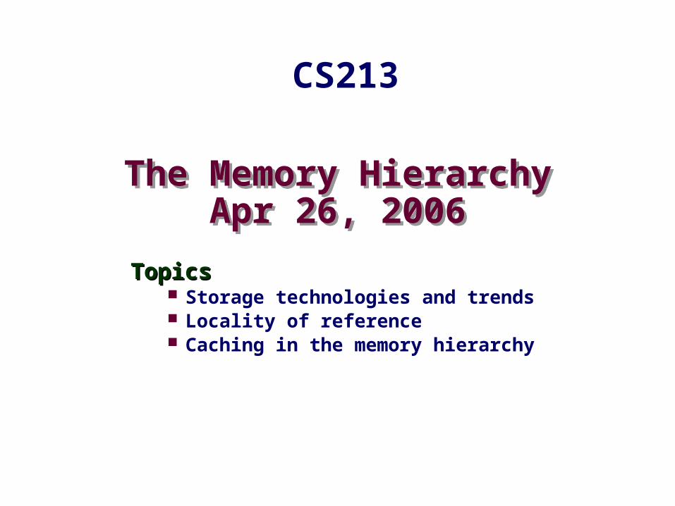
The Memory HierarchyApr 26, 2006
The Memory HierarchyApr 26, 2006
TopicsTopics Storage technologies and trends Locality of reference Caching in the memory hierarchy
CS213
– 2 – CS213, S’06
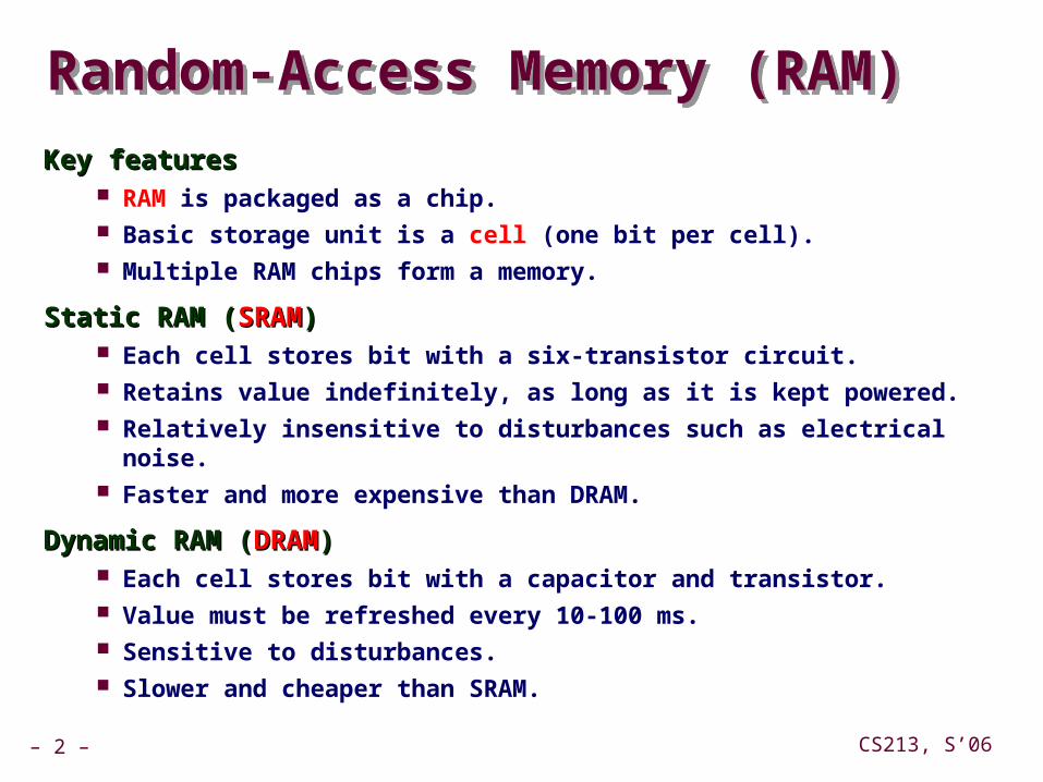
Random-Access Memory (RAM)Random-Access Memory (RAM)
Key featuresKey features RAM is packaged as a chip. Basic storage unit is a cell (one bit per cell). Multiple RAM chips form a memory.
Static RAM (Static RAM (SRAMSRAM)) Each cell stores bit with a six-transistor circuit. Retains value indefinitely, as long as it is kept powered. Relatively insensitive to disturbances such as electrical noise. Faster and more expensive than DRAM.
Dynamic RAM (Dynamic RAM (DRAMDRAM)) Each cell stores bit with a capacitor and transistor. Value must be refreshed every 10-100 ms. Sensitive to disturbances. Slower and cheaper than SRAM.
– 3 – CS213, S’06
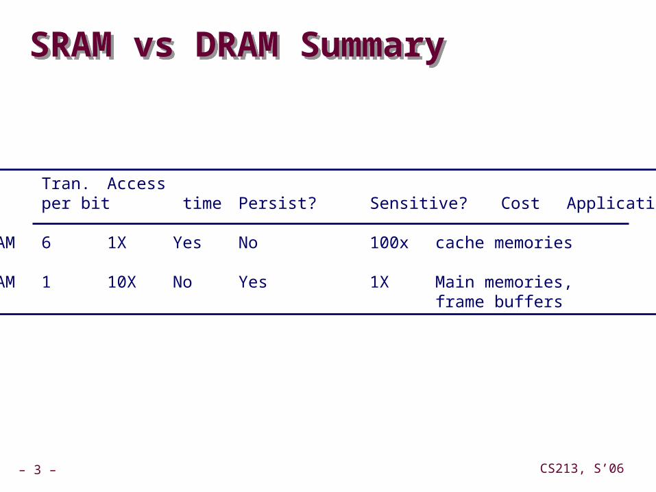
SRAM vs DRAM SummarySRAM vs DRAM Summary
Tran. Accessper bit time Persist? Sensitive? Cost Applications
SRAM 6 1X Yes No 100x cache memories
DRAM 1 10X No Yes 1X Main memories,frame buffers
– 4 – CS213, S’06
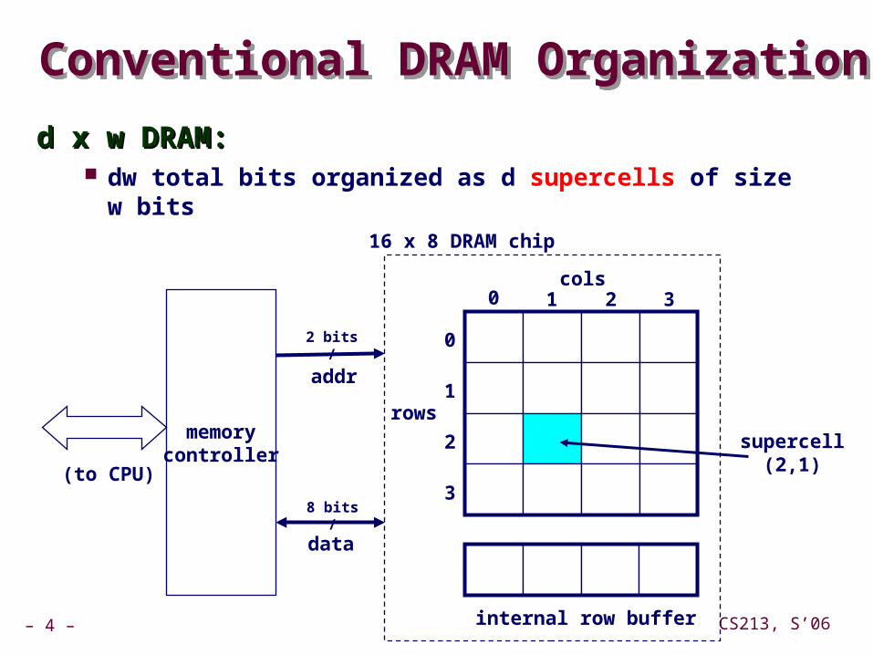
Conventional DRAM OrganizationConventional DRAM Organization
d x w DRAM:d x w DRAM: dw total bits organized as d supercells of size w bits
cols
rows
0 1 2 3
0
1
2
3
internal row buffer
16 x 8 DRAM chip
addr
data
supercell(2,1)
2 bits/
8 bits/
memorycontroller
(to CPU)
– 5 – CS213, S’06
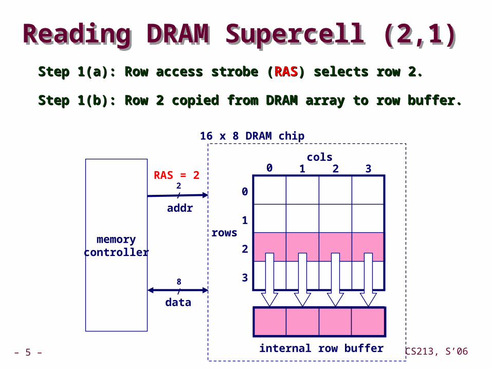
Reading DRAM Supercell (2,1)Reading DRAM Supercell (2,1)
Step 1(a): Row access strobe (Step 1(a): Row access strobe (RASRAS) selects row 2.) selects row 2.
cols
rows
RAS = 20 1 2 3
0
1
2
internal row buffer
16 x 8 DRAM chip
3
addr
data
2/
8/
memorycontroller
Step 1(b): Row 2 copied from DRAM array to row buffer.Step 1(b): Row 2 copied from DRAM array to row buffer.
– 6 – CS213, S’06
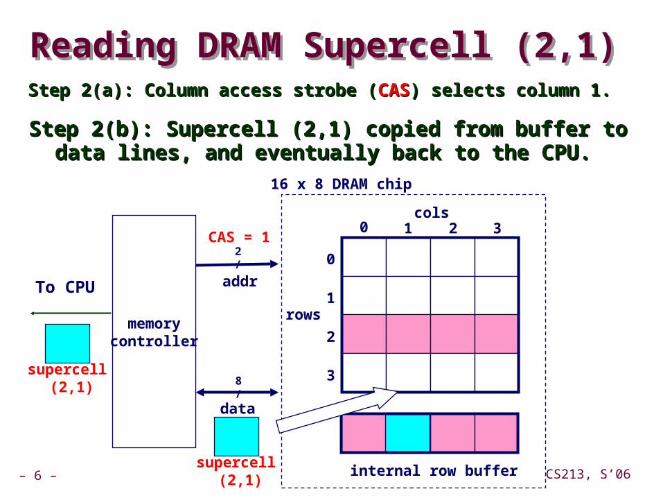
Reading DRAM Supercell (2,1)Reading DRAM Supercell (2,1)Step 2(a): Column access strobe (Step 2(a): Column access strobe (CASCAS) selects column 1.) selects column 1.
cols
rows
0 1 2 3
0
1
2
3
internal row buffer
16 x 8 DRAM chip
CAS = 1
addr
data
2/
8/
memorycontroller
Step 2(b): Supercell (2,1) copied from buffer to data lines, Step 2(b): Supercell (2,1) copied from buffer to data lines, and eventually back to the CPU.and eventually back to the CPU.
supercell (2,1)
supercell (2,1)
To CPU
– 7 – CS213, S’06
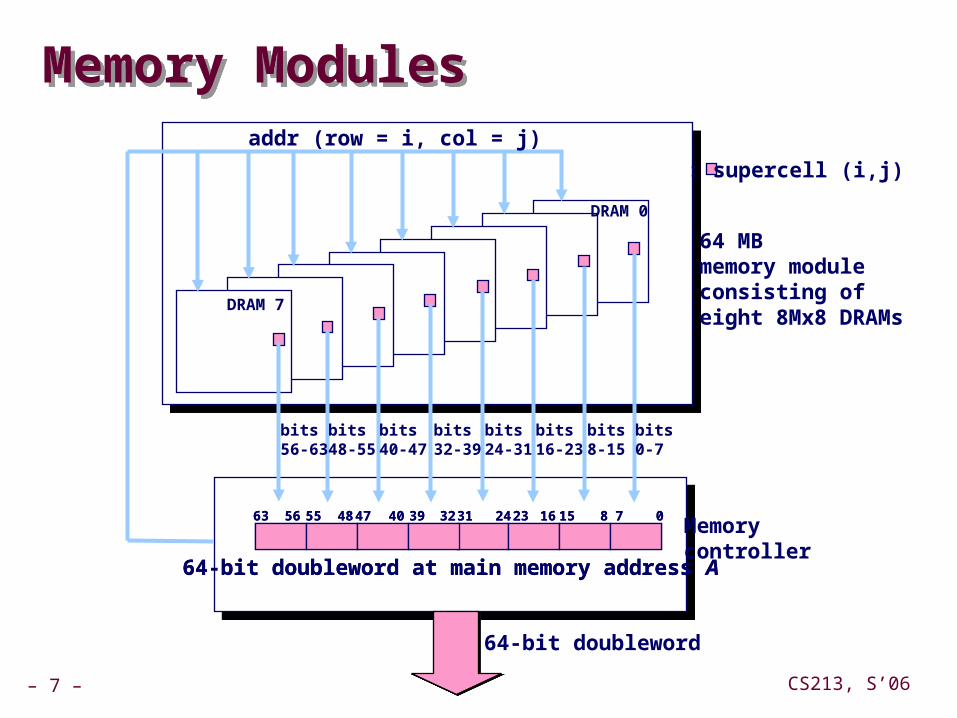
Memory ModulesMemory Modules
: supercell (i,j)
64 MB memory moduleconsisting ofeight 8Mx8 DRAMs
addr (row = i, col = j)
Memorycontroller
DRAM 7
DRAM 0
031 78151623243263 394047485556
64-bit doubleword at main memory address A
bits0-7
bits8-15
bits16-23
bits24-31
bits32-39
bits40-47
bits48-55
bits56-63
64-bit doubleword
031 78151623243263 394047485556
64-bit doubleword at main memory address A
– 8 – CS213, S’06
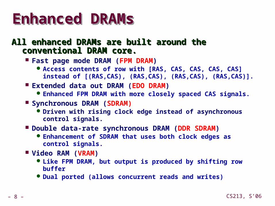
Enhanced DRAMsEnhanced DRAMs
All enhanced DRAMs are built around the conventional All enhanced DRAMs are built around the conventional DRAM core. DRAM core. Fast page mode DRAM (FPM DRAM)
Access contents of row with [RAS, CAS, CAS, CAS, CAS] instead of [(RAS,CAS), (RAS,CAS), (RAS,CAS), (RAS,CAS)].
Extended data out DRAM (EDO DRAM)Enhanced FPM DRAM with more closely spaced CAS signals.
Synchronous DRAM (SDRAM)Driven with rising clock edge instead of asynchronous control
signals. Double data-rate synchronous DRAM (DDR SDRAM)
Enhancement of SDRAM that uses both clock edges as control signals.
Video RAM (VRAM)Like FPM DRAM, but output is produced by shifting row bufferDual ported (allows concurrent reads and writes)
– 9 – CS213, S’06
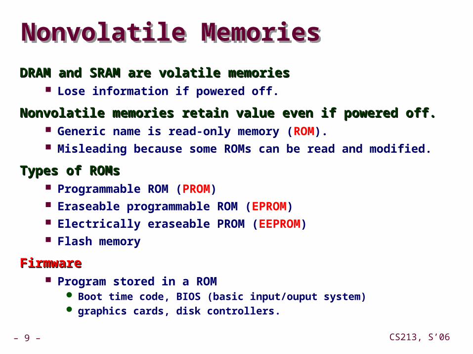
Nonvolatile MemoriesNonvolatile Memories
DRAM and SRAM are volatile memoriesDRAM and SRAM are volatile memories Lose information if powered off.
Nonvolatile memories retain value even if powered off.Nonvolatile memories retain value even if powered off. Generic name is read-only memory (ROM). Misleading because some ROMs can be read and modified.
Types of ROMsTypes of ROMs Programmable ROM (PROM) Eraseable programmable ROM (EPROM) Electrically eraseable PROM (EEPROM) Flash memory
FirmwareFirmware Program stored in a ROM
Boot time code, BIOS (basic input/ouput system) graphics cards, disk controllers.
– 10 – CS213, S’06
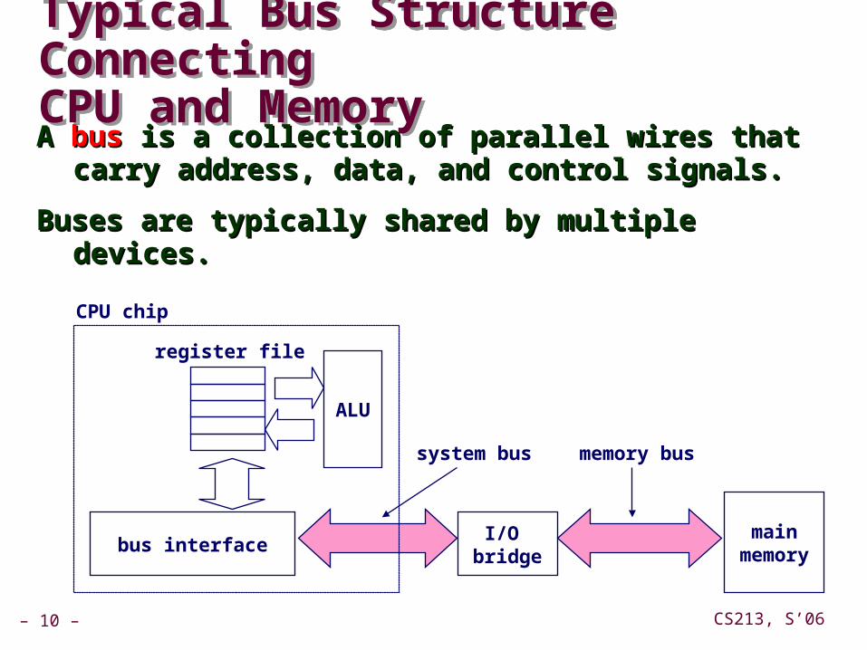
Typical Bus Structure Connecting CPU and MemoryTypical Bus Structure Connecting CPU and MemoryA A busbus is a collection of parallel wires that carry is a collection of parallel wires that carry
address, data, and control signals.address, data, and control signals.
Buses are typically shared by multiple devices.Buses are typically shared by multiple devices.
mainmemory
I/O bridge
bus interface
ALU
register file
CPU chip
system bus memory bus
– 11 – CS213, S’06
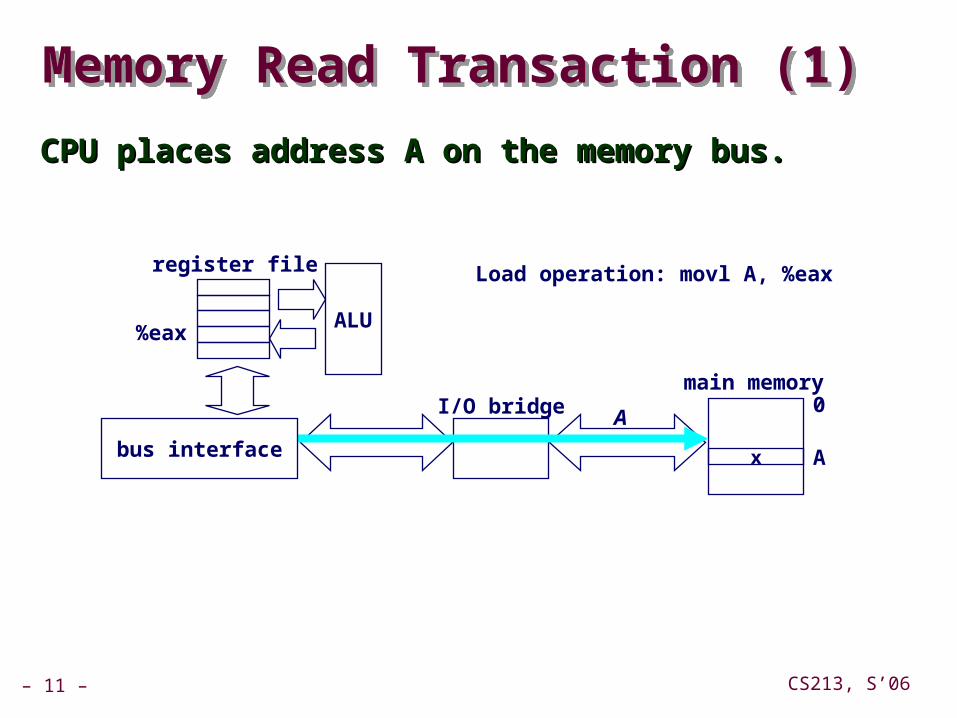
Memory Read Transaction (1)Memory Read Transaction (1)
CPU places address A on the memory bus.CPU places address A on the memory bus.
ALU
register file
bus interface
A0
Ax
main memoryI/O bridge
%eax
Load operation: movl A, %eax
– 12 – CS213, S’06
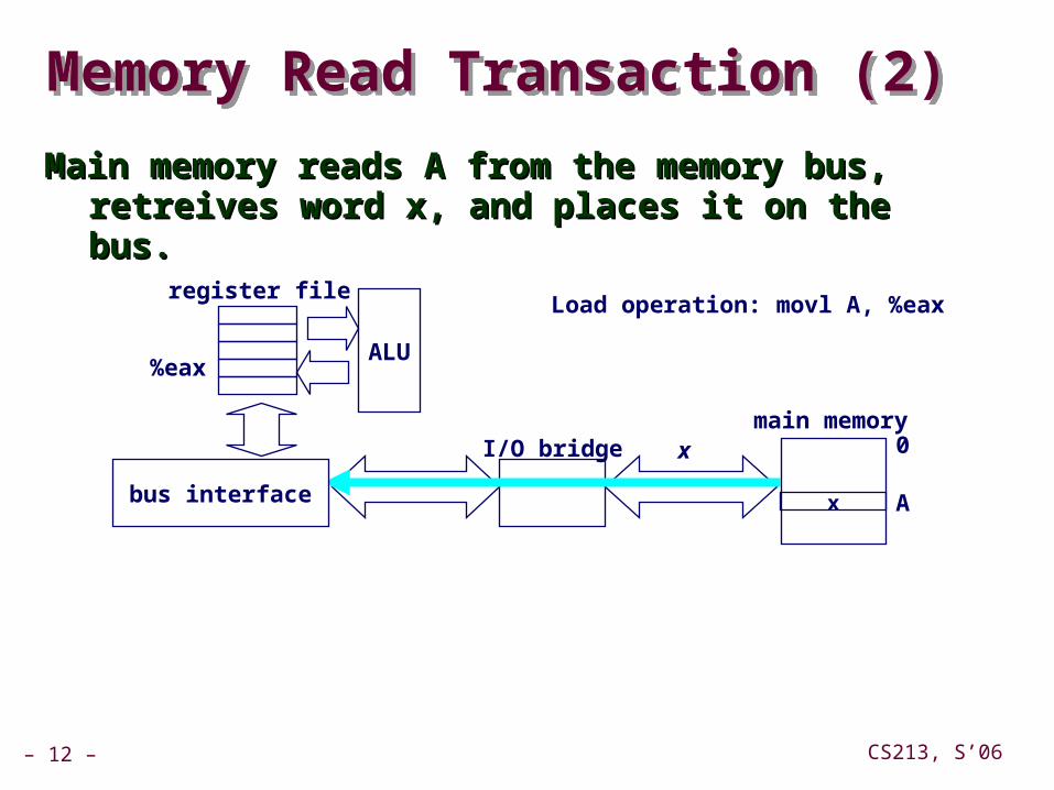
Memory Read Transaction (2)Memory Read Transaction (2)
Main memory reads A from the memory bus, retreives Main memory reads A from the memory bus, retreives word x, and places it on the bus.word x, and places it on the bus.
ALU
register file
bus interface
x 0
Ax
main memory
%eax
I/O bridge
Load operation: movl A, %eax
– 13 – CS213, S’06
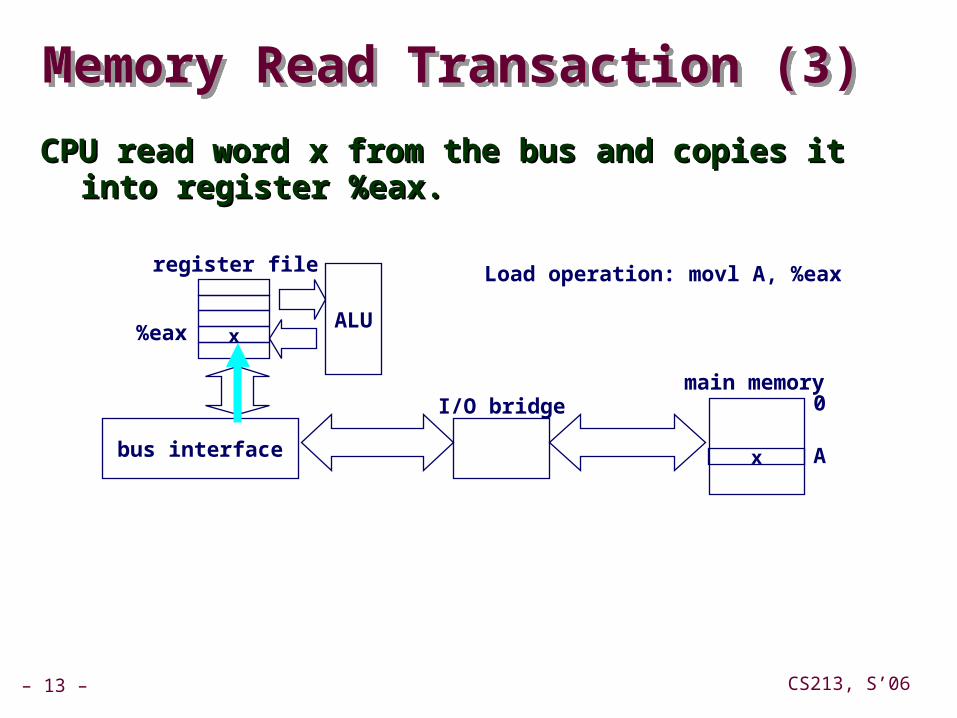
Memory Read Transaction (3)Memory Read Transaction (3)
CPU read word x from the bus and copies it into CPU read word x from the bus and copies it into register %eax.register %eax.
xALU
register file
bus interface x
main memory0
A
%eax
I/O bridge
Load operation: movl A, %eax
– 14 – CS213, S’06
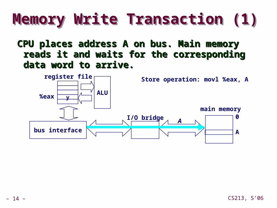
Memory Write Transaction (1)Memory Write Transaction (1)
CPU places address A on bus. Main memory reads it CPU places address A on bus. Main memory reads it and waits for the corresponding data word to arrive.and waits for the corresponding data word to arrive.
yALU
register file
bus interface
A
main memory0
A
%eax
I/O bridge
Store operation: movl %eax, A
– 15 – CS213, S’06
Memory Write Transaction (2)Memory Write Transaction (2)
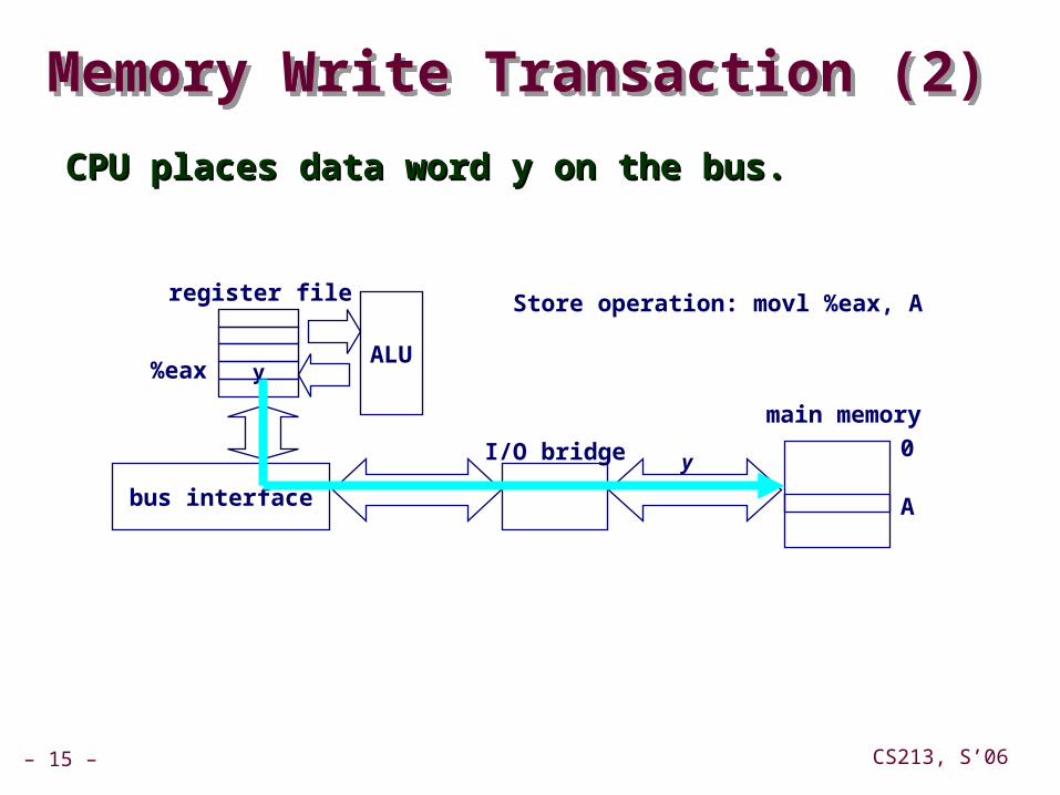
CPU places data word y on the bus.CPU places data word y on the bus.
yALU
register file
bus interface
y
main memory
0
A
%eax
I/O bridge
Store operation: movl %eax, A
– 16 – CS213, S’06
Memory Write Transaction (3)Memory Write Transaction (3)
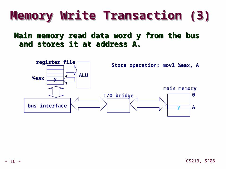
Main memory read data word y from the bus and stores Main memory read data word y from the bus and stores it at address A.it at address A.
yALU
register file
bus interface y
main memory0
A
%eax
I/O bridge
Store operation: movl %eax, A
– 17 – CS213, S’06
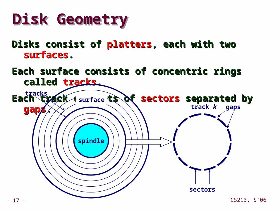
Disk GeometryDisk Geometry
Disks consist of Disks consist of plattersplatters, each with two , each with two surfacessurfaces..
Each surface consists of concentric rings called Each surface consists of concentric rings called trackstracks..
Each track consists of Each track consists of sectorssectors separated by separated by gapsgaps..
spindle
surfacetracks
track k
sectors
gaps
– 18 – CS213, S’06
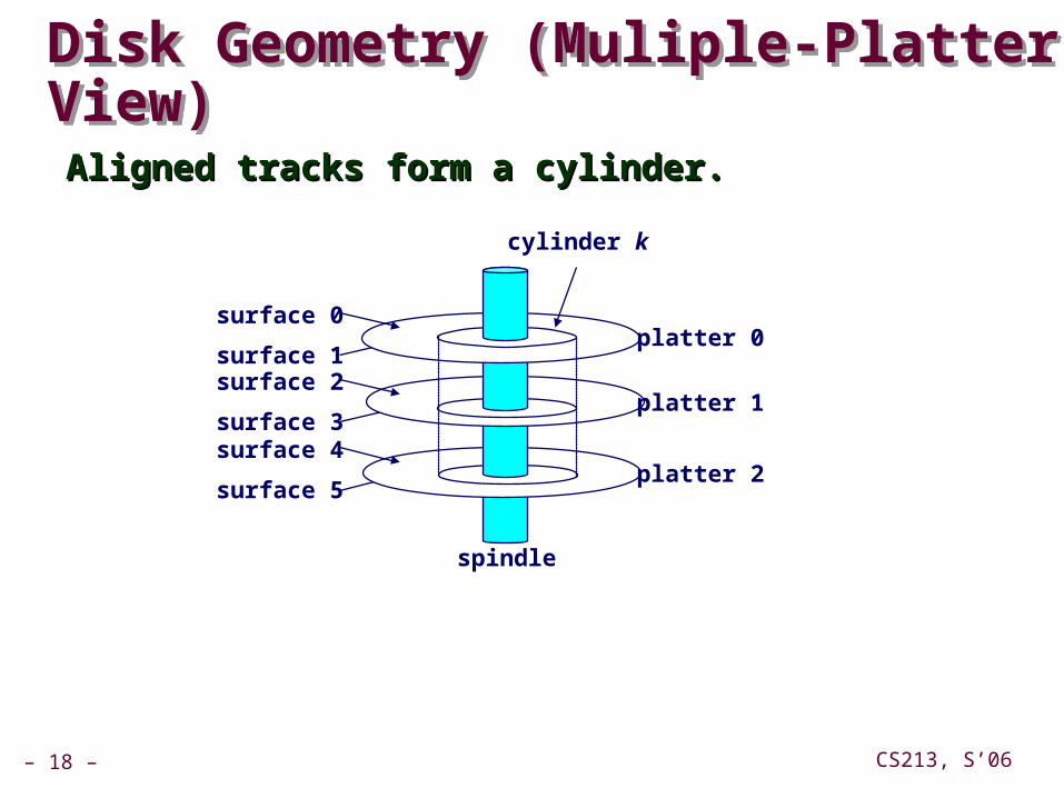
Disk Geometry (Muliple-Platter View)Disk Geometry (Muliple-Platter View)
Aligned tracks form a cylinder.Aligned tracks form a cylinder.
surface 0
surface 1surface 2
surface 3surface 4
surface 5
cylinder k
spindle
platter 0
platter 1
platter 2
– 19 – CS213, S’06
Disk CapacityDisk Capacity
Capacity:Capacity: maximum number of bits that can be stored. maximum number of bits that can be stored. Vendors express capacity in units of gigabytes (GB), where 1 GB =
10^9.
Capacity is determined by these technology factors:Capacity is determined by these technology factors: Recording density (bits/in): number of bits that can be squeezed
into a 1 inch segment of a track. Track density (tracks/in): number of tracks that can be squeezed
into a 1 inch radial segment. Areal density (bits/in2): product of recording and track density.
Modern disks partition tracks into disjoint subsets called Modern disks partition tracks into disjoint subsets called recording zonesrecording zones Each track in a zone has the same number of sectors, determined
by the circumference of innermost track. Each zone has a different number of sectors/track
– 20 – CS213, S’06
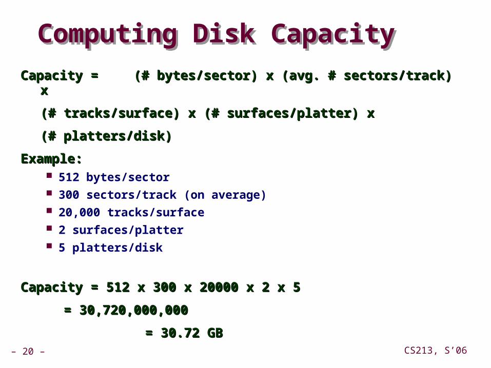
Computing Disk Capacity Computing Disk Capacity
Capacity = Capacity = (# bytes/sector) x (avg. # sectors/track) x(# bytes/sector) x (avg. # sectors/track) x
(# tracks/surface) x (# surfaces/platter) x(# tracks/surface) x (# surfaces/platter) x
(# platters/disk)(# platters/disk)
Example:Example: 512 bytes/sector 300 sectors/track (on average) 20,000 tracks/surface 2 surfaces/platter 5 platters/disk
Capacity = 512 x 300 x 20000 x 2 x 5Capacity = 512 x 300 x 20000 x 2 x 5
= 30,720,000,000= 30,720,000,000
= 30.72 GB = 30.72 GB
– 21 – CS213, S’06
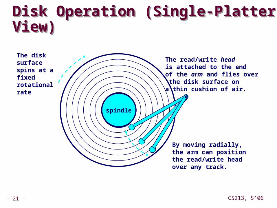
Disk Operation (Single-Platter View)Disk Operation (Single-Platter View)
The disk surface spins at a fixedrotational rate
spindle
By moving radially, the arm can position the read/write head over any track.
The read/write headis attached to the endof the arm and flies over the disk surface ona thin cushion of air.
spin
dle
spindle
spin
dle
spindle
– 22 – CS213, S’06
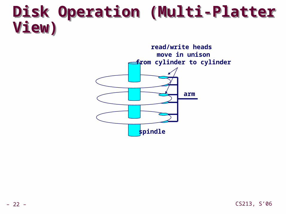
Disk Operation (Multi-Platter View)Disk Operation (Multi-Platter View)
arm
read/write heads move in unison
from cylinder to cylinder
spindle
– 23 – CS213, S’06
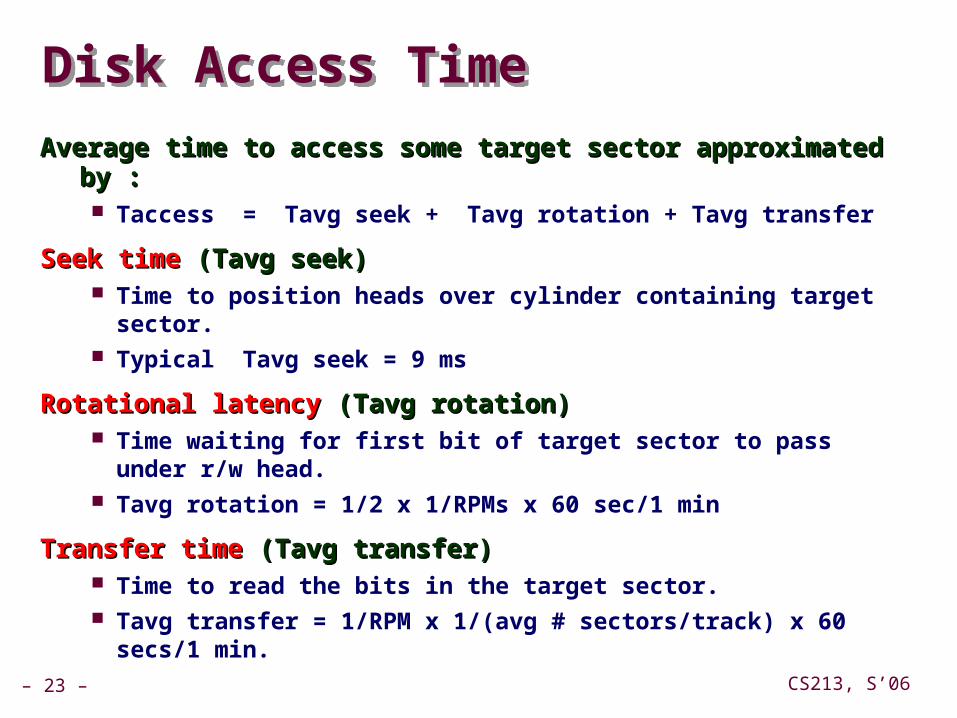
Disk Access TimeDisk Access Time
Average time to access some target sector approximated by :Average time to access some target sector approximated by : Taccess = Tavg seek + Tavg rotation + Tavg transfer
Seek timeSeek time (Tavg seek) (Tavg seek) Time to position heads over cylinder containing target sector. Typical Tavg seek = 9 ms
Rotational latencyRotational latency (Tavg rotation) (Tavg rotation) Time waiting for first bit of target sector to pass under r/w head. Tavg rotation = 1/2 x 1/RPMs x 60 sec/1 min
Transfer timeTransfer time (Tavg transfer) (Tavg transfer) Time to read the bits in the target sector. Tavg transfer = 1/RPM x 1/(avg # sectors/track) x 60 secs/1 min.
– 24 – CS213, S’06
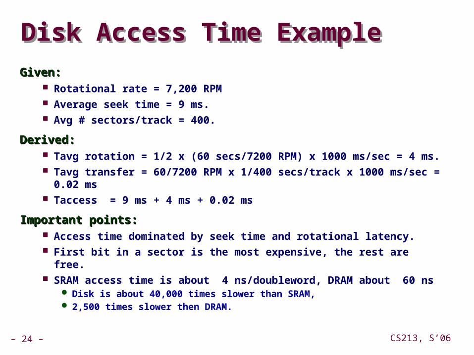
Disk Access Time ExampleDisk Access Time Example
Given:Given: Rotational rate = 7,200 RPM Average seek time = 9 ms. Avg # sectors/track = 400.
Derived:Derived: Tavg rotation = 1/2 x (60 secs/7200 RPM) x 1000 ms/sec = 4 ms. Tavg transfer = 60/7200 RPM x 1/400 secs/track x 1000 ms/sec =
0.02 ms Taccess = 9 ms + 4 ms + 0.02 ms
Important points:Important points: Access time dominated by seek time and rotational latency. First bit in a sector is the most expensive, the rest are free. SRAM access time is about 4 ns/doubleword, DRAM about 60 ns
Disk is about 40,000 times slower than SRAM, 2,500 times slower then DRAM.
– 25 – CS213, S’06
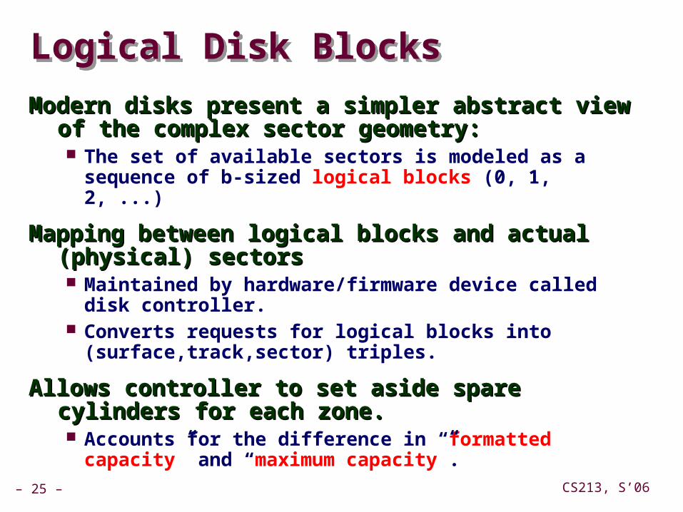
Logical Disk BlocksLogical Disk Blocks
Modern disks present a simpler abstract view of the Modern disks present a simpler abstract view of the complex sector geometry:complex sector geometry: The set of available sectors is modeled as a sequence of b-
sized logical blocks (0, 1, 2, ...)
Mapping between logical blocks and actual (physical) Mapping between logical blocks and actual (physical) sectorssectors Maintained by hardware/firmware device called disk
controller. Converts requests for logical blocks into
(surface,track,sector) triples.
Allows controller to set aside spare cylinders for each Allows controller to set aside spare cylinders for each zone.zone. Accounts for the difference in “formatted capacity” and
“maximum capacity”.
– 26 – CS213, S’06
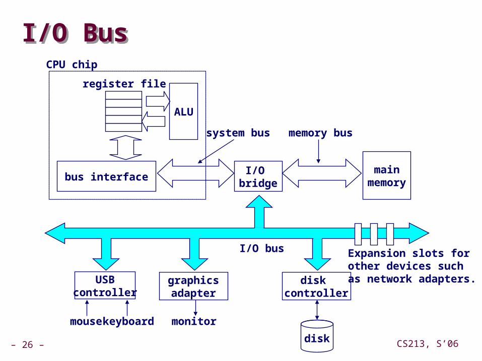
I/O BusI/O Bus
mainmemory
I/O bridge
bus interface
ALU
register file
CPU chip
system bus memory bus
disk controller
graphicsadapter
USBcontroller
mousekeyboard monitor
disk
I/O bus Expansion slots forother devices suchas network adapters.
– 27 – CS213, S’06
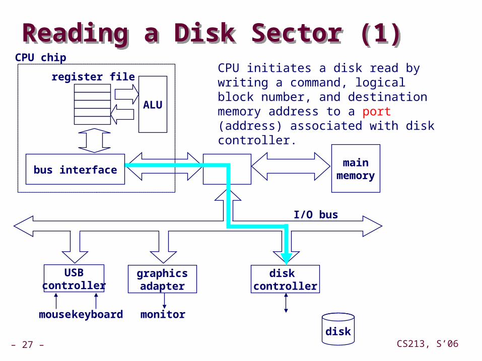
Reading a Disk Sector (1)Reading a Disk Sector (1)
mainmemory
ALU
register file
CPU chip
disk controller
graphicsadapter
USBcontroller
mousekeyboard monitor
disk
I/O bus
bus interface
CPU initiates a disk read by writing a command, logical block number, and destination memory address to a port (address) associated with disk controller.
– 28 – CS213, S’06
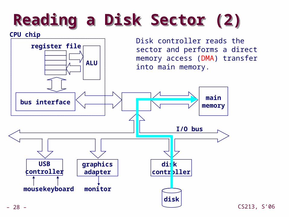
Reading a Disk Sector (2)Reading a Disk Sector (2)
mainmemory
ALU
register file
CPU chip
disk controller
graphicsadapter
USBcontroller
mousekeyboard monitor
disk
I/O bus
bus interface
Disk controller reads the sector and performs a direct memory access (DMA) transfer into main memory.
– 29 – CS213, S’06
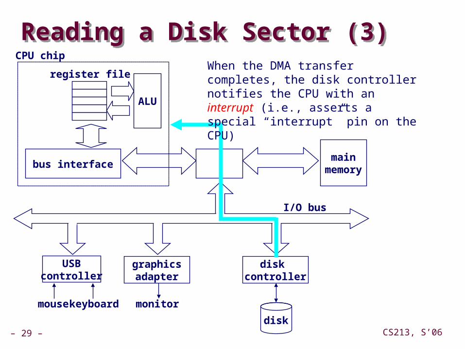
Reading a Disk Sector (3)Reading a Disk Sector (3)
mainmemory
ALU
register file
CPU chip
disk controller
graphicsadapter
USBcontroller
mousekeyboard monitor
disk
I/O bus
bus interface
When the DMA transfer completes, the disk controller notifies the CPU with an interrupt (i.e., asserts a special “interrupt” pin on the CPU)
– 30 – CS213, S’06
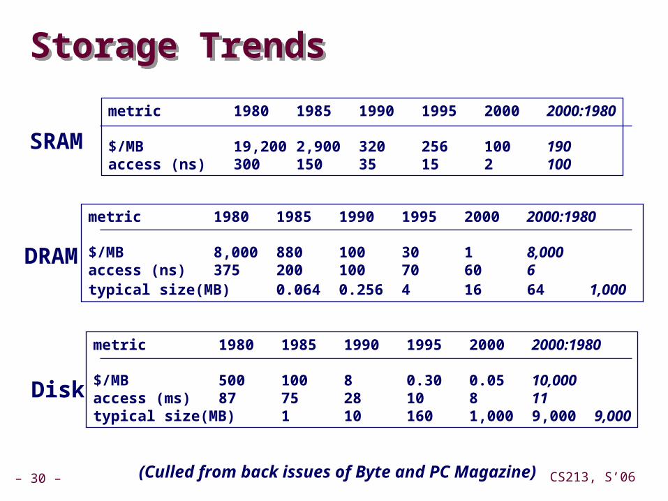
Storage TrendsStorage Trends
(Culled from back issues of Byte and PC Magazine)
metric 1980 1985 1990 1995 2000 2000:1980
$/MB 8,000 880 100 30 1 8,000access (ns) 375 200 100 70 60 6typical size(MB) 0.064 0.256 4 16 64 1,000
DRAM
metric 1980 1985 1990 1995 2000 2000:1980
$/MB 19,200 2,900 320 256 100 190access (ns) 300 150 35 15 2 100
SRAM
metric 1980 1985 1990 1995 2000 2000:1980
$/MB 500 100 8 0.30 0.05 10,000access (ms) 87 75 28 10 8 11typical size(MB) 1 10 160 1,000 9,000 9,000
Disk
– 31 – CS213, S’06
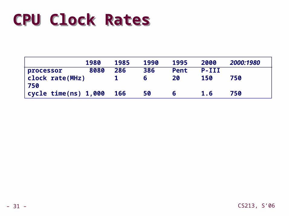
CPU Clock RatesCPU Clock Rates
1980 1985 1990 1995 2000 2000:1980processor 8080 286 386 Pent P-IIIclock rate(MHz) 1 6 20 150 750 750cycle time(ns) 1,000 166 50 6 1.6 750
– 32 – CS213, S’06
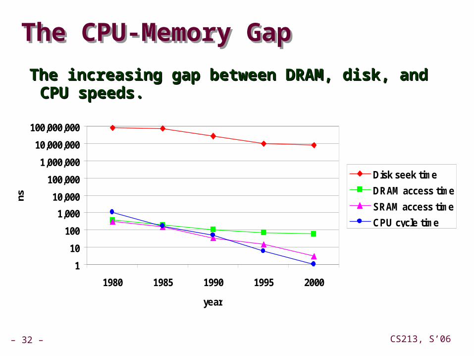
The CPU-Memory GapThe CPU-Memory Gap
The increasing gap between DRAM, disk, and CPU The increasing gap between DRAM, disk, and CPU speeds.speeds.
1
10
100
1,000
10,000
100,000
1,000,000
10,000,000
100,000,000
1980 1985 1990 1995 2000
year
ns
Disk seek time
DRAM access time
SRAM access time
CPU cycle time
– 33 – CS213, S’06
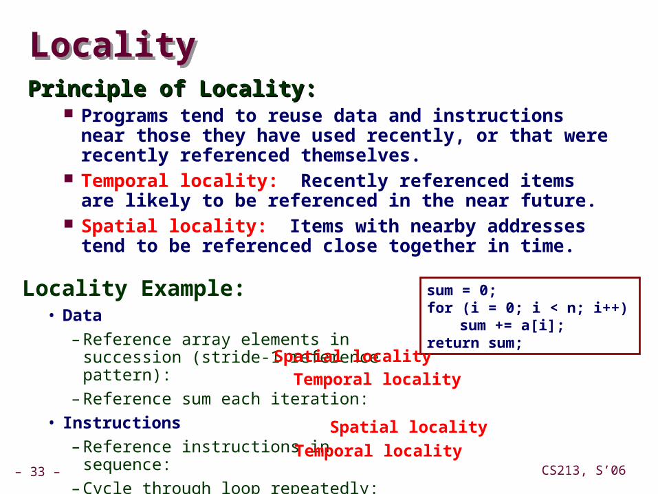
LocalityLocalityPrinciple of Locality:Principle of Locality:
Programs tend to reuse data and instructions near those they have used recently, or that were recently referenced themselves.
Temporal locality: Recently referenced items are likely to be referenced in the near future.
Spatial locality: Items with nearby addresses tend to be referenced close together in time.
Locality Example:• Data
– Reference array elements in succession (stride-1 reference pattern):
– Reference sum each iteration:
• Instructions
– Reference instructions in sequence:
– Cycle through loop repeatedly:
sum = 0;for (i = 0; i < n; i++)
sum += a[i];return sum;
Spatial locality
Spatial locality
Temporal locality
Temporal locality
– 34 – CS213, S’06
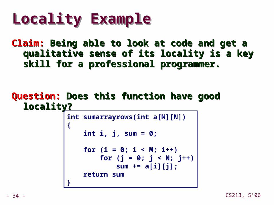
Locality ExampleLocality Example
Claim:Claim: Being able to look at code and get a qualitative Being able to look at code and get a qualitative sense of its locality is a key skill for a professional sense of its locality is a key skill for a professional programmer.programmer.
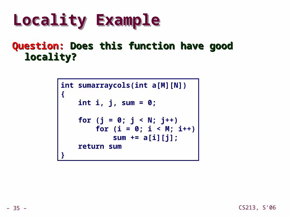
Question:Question: Does this function have good locality? Does this function have good locality?
int sumarrayrows(int a[M][N]){ int i, j, sum = 0;
for (i = 0; i < M; i++) for (j = 0; j < N; j++) sum += a[i][j]; return sum}
– 35 – CS213, S’06
Locality ExampleLocality Example
Question:Question: Does this function have good locality? Does this function have good locality?
int sumarraycols(int a[M][N]){ int i, j, sum = 0;
for (j = 0; j < N; j++) for (i = 0; i < M; i++) sum += a[i][j]; return sum}
– 36 – CS213, S’06
Locality ExampleLocality Example
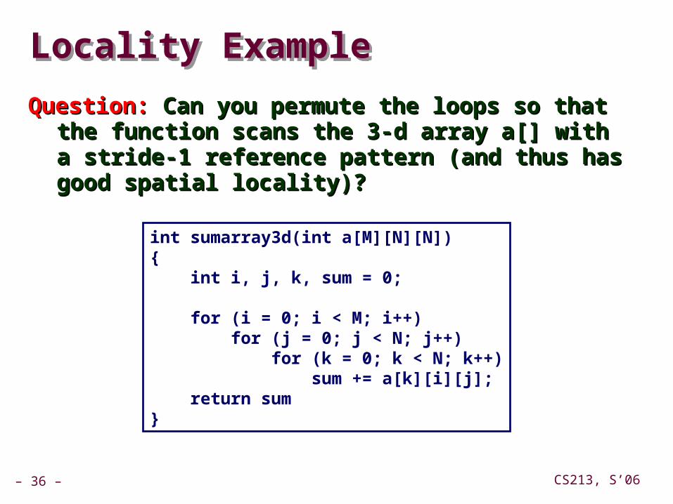
Question:Question: Can you permute the loops so that the Can you permute the loops so that the function scans the 3-d array function scans the 3-d array a[]a[] with a stride-1 with a stride-1 reference pattern (and thus has good spatial reference pattern (and thus has good spatial locality)?locality)?
int sumarray3d(int a[M][N][N]){ int i, j, k, sum = 0;
for (i = 0; i < M; i++) for (j = 0; j < N; j++) for (k = 0; k < N; k++) sum += a[k][i][j]; return sum}
– 37 – CS213, S’06
Memory HierarchiesMemory Hierarchies
Some fundamental and enduring properties of Some fundamental and enduring properties of hardware and software:hardware and software: Fast storage technologies cost more per byte and have less
capacity. The gap between CPU and main memory speed is widening. Well-written programs tend to exhibit good locality.
These fundamental properties complement each other These fundamental properties complement each other beautifully.beautifully.
They suggest an approach for organizing memory and They suggest an approach for organizing memory and storage systems known as a storage systems known as a memory hierarchymemory hierarchy..
– 38 – CS213, S’06
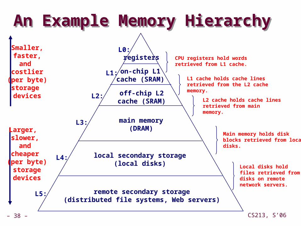
An Example Memory HierarchyAn Example Memory Hierarchy
registers
on-chip L1cache (SRAM)
main memory(DRAM)
local secondary storage(local disks)
Larger, slower,
and cheaper (per byte)storagedevices
remote secondary storage(distributed file systems, Web servers)
Local disks hold files retrieved from disks on remote network servers.
Main memory holds disk blocks retrieved from local disks.
off-chip L2cache (SRAM)
L1 cache holds cache lines retrieved from the L2 cache memory.
CPU registers hold words retrieved from L1 cache.
L2 cache holds cache lines retrieved from main memory.
L0:
L1:
L2:
L3:
L4:
L5:
Smaller,faster,and
costlier(per byte)storage devices
– 39 – CS213, S’06
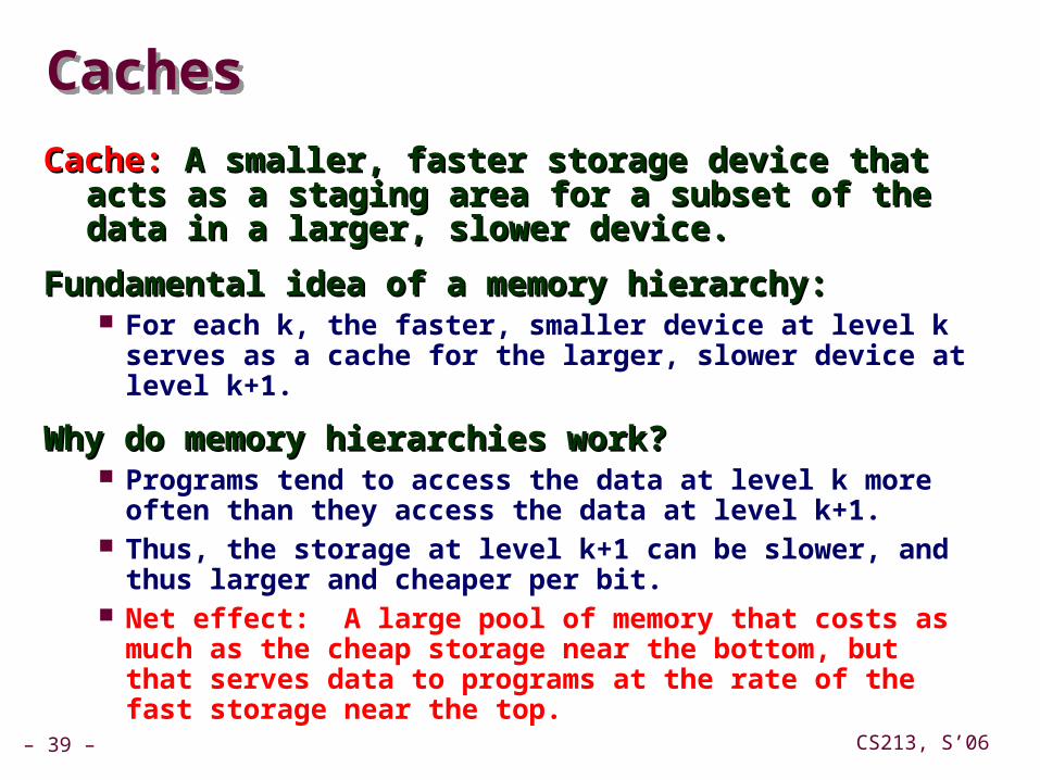
CachesCaches
Cache:Cache: A smaller, faster storage device that acts as a A smaller, faster storage device that acts as a staging area for a subset of the data in a larger, staging area for a subset of the data in a larger, slower device.slower device.
Fundamental idea of a memory hierarchy:Fundamental idea of a memory hierarchy: For each k, the faster, smaller device at level k serves as a
cache for the larger, slower device at level k+1.
Why do memory hierarchies work?Why do memory hierarchies work? Programs tend to access the data at level k more often than
they access the data at level k+1. Thus, the storage at level k+1 can be slower, and thus larger
and cheaper per bit. Net effect: A large pool of memory that costs as much as
the cheap storage near the bottom, but that serves data to programs at the rate of the fast storage near the top.
– 40 – CS213, S’06
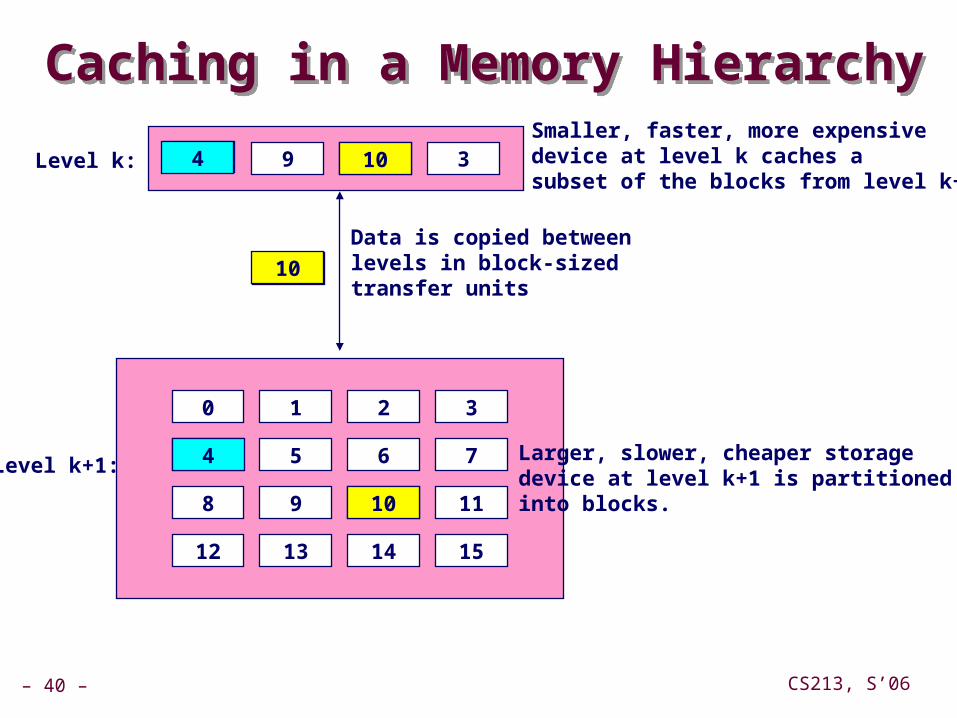
Caching in a Memory HierarchyCaching in a Memory Hierarchy
0 1 2 3
4 5 6 7
8 9 10 11
12 13 14 15
Larger, slower, cheaper storagedevice at level k+1 is partitionedinto blocks.
Data is copied betweenlevels in block-sized transfer units
8 9 14 3Smaller, faster, more expensivedevice at level k caches a subset of the blocks from level k+1
Level k:
Level k+1: 4
4
4 10
10
10
– 41 – CS213, S’06
Request14
Request12
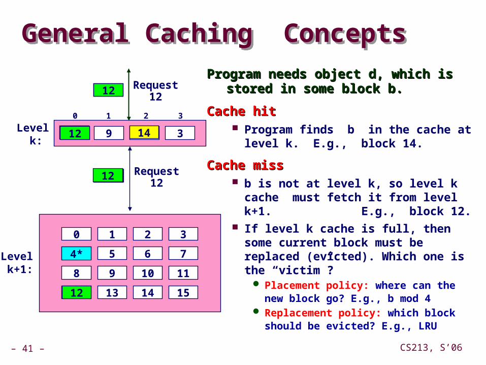
General Caching ConceptsGeneral Caching Concepts
Program needs object d, which is stored Program needs object d, which is stored in some block b.in some block b.
Cache hitCache hit Program finds b in the cache at level
k. E.g., block 14.
Cache missCache miss b is not at level k, so level k cache
must fetch it from level k+1. E.g., block 12.
If level k cache is full, then some current block must be replaced (evicted). Which one is the “victim”?
Placement policy: where can the new block go? E.g., b mod 4
Replacement policy: which block should be evicted? E.g., LRU
9 3
0 1 2 3
4 5 6 7
8 9 10 11
12 13 14 15
Level k:
Level k+1:
1414
12
14
4*
4*12
12
0 1 2 3
Request12
4*4*12
– 42 – CS213, S’06
General Caching ConceptsGeneral Caching Concepts
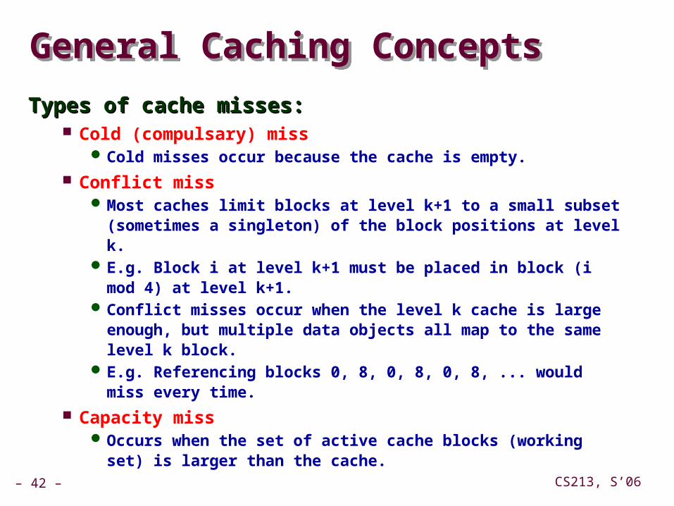
Types of cache misses:Types of cache misses: Cold (compulsary) miss
Cold misses occur because the cache is empty.
Conflict missMost caches limit blocks at level k+1 to a small subset
(sometimes a singleton) of the block positions at level k.E.g. Block i at level k+1 must be placed in block (i mod 4) at
level k+1.Conflict misses occur when the level k cache is large enough,
but multiple data objects all map to the same level k block.E.g. Referencing blocks 0, 8, 0, 8, 0, 8, ... would miss every time.
Capacity missOccurs when the set of active cache blocks (working set) is
larger than the cache.
– 43 – CS213, S’06
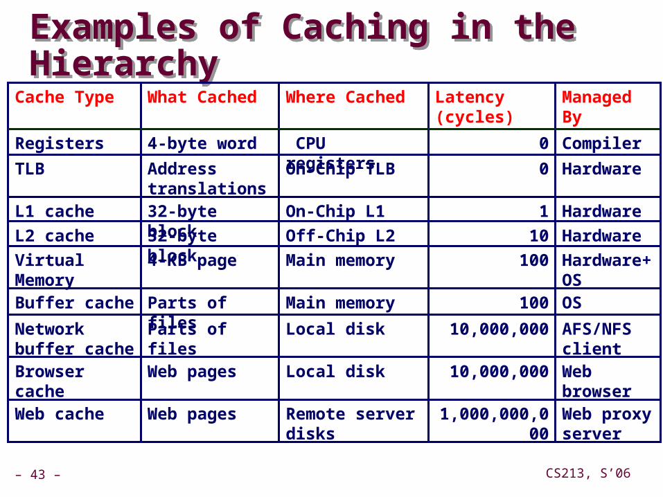
Examples of Caching in the HierarchyExamples of Caching in the Hierarchy
Hardware0On-Chip TLBAddress translations
TLB
Web browser
10,000,000Local diskWeb pagesBrowser cache
Web cache
Network buffer cache
Buffer cache
Virtual Memory
L2 cache
L1 cache
Registers
Cache Type
Web pages
Parts of files
Parts of files
4-KB page
32-byte block
32-byte block
4-byte word
What Cached
Web proxy server
1,000,000,000Remote server disks
OS100Main memory
Hardware1On-Chip L1
Hardware10Off-Chip L2
AFS/NFS client
10,000,000Local disk
Hardware+OS
100Main memory
Compiler0 CPU registers
Managed By
Latency (cycles)
Where Cached