Embed Size (px)
Citation preview
8 SPRING 20 19 IEEE SOLID-STATE CIRCUITS MAGAZINE
A CIRCUIT FOR ALL SEASONS
Behzad Razavi
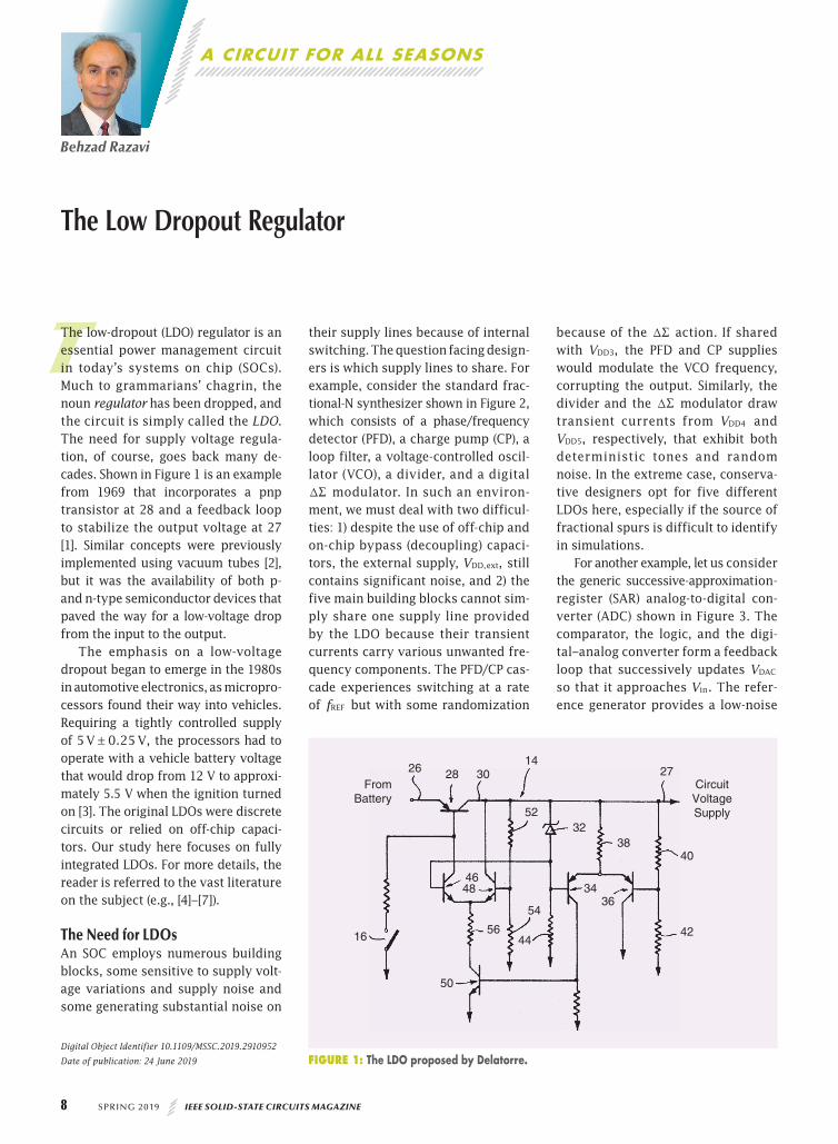
TThe low-dropout (LDO) regulator is an essential power management circuit in today’s systems on chip (SOCs). Much to grammarians’ chagrin, the noun regulator has been dropped, and the circuit is simply called the LDO. The need for supply voltage regula-tion, of course, goes back many de-cades. Shown in Figure 1 is an example from 1969 that incorporates a pnp transistor at 28 and a feedback loop to stabilize the output voltage at 27 [1]. Similar concepts were previously implemented using vacuum tubes [2], but it was the availability of both p- and n-type semiconductor devices that paved the way for a low-voltage drop from the input to the output.
The emphasis on a low-voltage dropout began to emerge in the 1980s in automotive electronics, as micropro-cessors found their way into vehicles. Requiring a tightly controlled supply of ,5V 0.25V! the processors had to operate with a vehicle battery voltage that would drop from 12 V to approxi-mately 5.5 V when the ignition turned on [3]. The original LDOs were discrete circuits or relied on off-chip capaci-tors. Our study here focuses on fully integrated LDOs. For more details, the reader is referred to the vast literature on the subject (e.g., [4]–[7]).
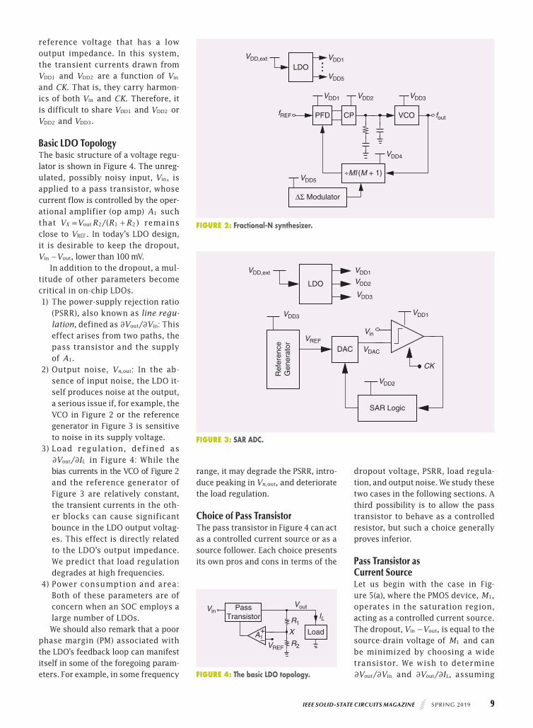
The Need for LDOsAn SOC employs numerous building blocks, some sensitive to supply volt-age variations and supply noise and some generating substantial noise on
their supply lines because of internal switching. The question facing design-ers is which supply lines to share. For example, consider the standard frac-tional-N synthesizer shown in Figure 2, which consists of a phase/frequency detector (PFD), a charge pump (CP), a loop filter, a voltage-controlled oscil-lator (VCO), a divider, and a digital TR modulator. In such an environ-ment, we must deal with two difficul-ties: 1) despite the use of off-chip and on-chip bypass (decoupling) capaci-tors, the external supply, ,V ,DD ext still contains significant noise, and 2) the five main building blocks cannot sim-ply share one supply line provided by the LDO because their transient currents carry various unwanted fre-quency components. The PFD/CP cas-cade experiences switching at a rate of fREF but with some randomization
because of the TR action. If shared with ,V 3DD the PFD and CP supplies would modulate the VCO frequency, corrupting the output. Similarly, the divider and the TR modulator draw transient currents from V 4DD and
,V 5DD respectively, that exhibit both deterministic tones and random noise. In the extreme case, conserva-tive designers opt for five different LDOs here, especially if the source of fractional spurs is difficult to identify in simulations.
For another example, let us consider the generic successive-approximation-register (SAR) analog-to-digital con-verter (ADC) shown in Figure 3. The comparator, the logic, and the digi-tal–analog converter form a feedback loop that successively updates VDAC so that it approaches .Vin The refer-ence generator provides a low-noise
Digital Object Identifier 10.1109/MSSC.2019.2910952
Date of publication: 24 June 2019
The Low Dropout Regulator
FromBattery
CircuitVoltageSupply
26 28 3014
27
40
42
3832
52
4648
56
54
44
50
16
3436
FIGURE 1: The LDO proposed by Delatorre.
IEEE SOLID-STATE CIRCUITS MAGAZINE SPRING 20 19 9
reference voltage that has a low output impedance. In this system, the transient currents drawn from V 1DD and V 2DD are a function of Vin and .CK That is, they carry harmon-ics of both Vin and .CK Therefore, it is difficult to share V 1DD and V 2DD or V 2DD and .V 3DD
Basic LDO TopologyThe basic structure of a voltage regu-lator is shown in Figure 4. The unreg-ulated, possibly noisy input, ,Vin is applied to a pass transistor, whose current flow is controlled by the oper-ational amplifier (op amp) A1 such that /( )V V R R R2 1 2outX = + remains close to .VREF In today’s LDO design, it is desirable to keep the dropout,
,V Vin out- lower than 100 mV.In addition to the dropout, a mul-
titude of other parameters become critical in on-chip LDOs.1) The power-supply rejection ratio
(PSRR), also known as line regu-lation, defined as / :V Vout in2 2 This effect arises from two paths, the pass transistor and the supply of .A1
2) Output noise, :V ,n out In the ab-sence of input noise, the LDO it-self produces noise at the output, a serious issue if, for example, the VCO in Figure 2 or the reference generator in Figure 3 is sensitive to noise in its supply voltage.
3) Load regulation, defined as /V ILout2 2 in Figure 4: While the
bias currents in the VCO of Figure 2 and the reference generator of Figure 3 are relatively constant, the transient currents in the oth-er blocks can cause significant bounce in the LDO output voltag-es. This effect is directly related to the LDO’s output impedance. We predict that load regulation degrades at high frequencies.
4) Power consumption and area: Both of these parameters are of concern when an SOC employs a large number of LDOs.We should also remark that a poor
phase margin (PM) associated with the LDO’s feedback loop can manifest itself in some of the foregoing param-eters. For example, in some frequency
range, it may degrade the PSRR, intro-duce peaking in ,V ,n out and deteriorate the load regulation.
Choice of Pass TransistorThe pass transistor in Figure 4 can act as a controlled current source or as a source follower. Each choice presents its own pros and cons in terms of the
dropout voltage, PSRR, load regula-tion, and output noise. We study these two cases in the following sections. A third possibility is to allow the pass transistor to behave as a controlled resistor, but such a choice generally proves inferior.
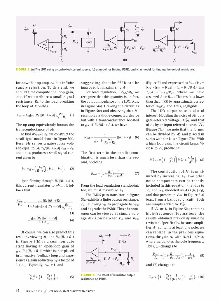
Pass Transistor as Current SourceLet us begin with the case in Fig-ure 5(a), where the PMOS device, ,M1 operates in the saturation region, acting as a controlled current source. The dropout, ,V Vin out- is equal to the source-drain voltage of M1 and can be minimized by choosing a wide transistor. We wish to determine
/V Vout in2 2 and / ,V ILout2 2 assuming
VCOfREF fout
∆Σ Modulator
LDO
PFD CP
VDD,ext VDD1
VDD1 VDD2 VDD3
VDD4
VDD5
VDD5
÷MI (M + 1)
FIGURE 2: Fractional-N synthesizer.
VREF
VDD,ext VDD1
VDD1
VDD2
Vin
VDD2
VDAC
VDD3
VDD3
DAC
SAR Logic
Ref
eren
ceG
ener
ator
LDO
CK
FIGURE 3: SAR ADC.
PassTransistor
Load
VinVout
VREF
ILR1
R2
XA1+–
FIGURE 4: The basic LDO topology.
10 SPRING 20 19 IEEE SOLID-STATE CIRCUITS MAGAZINE
for now that op amp A1 has infinite supply rejection. To this end, we should first compute the loop gain,
.ALG If we attribute a small-signal resistance, ,RL to the load, breaking the loop at X yields
[ ( )] .A A g R R R R RR
LG m L1 1 1 21 2
2<= ++
(1)
The op amp equivalently boosts the transconductance of .M1
To find / ,V Vout in2 2 we construct the small-signal model shown in Figure 5(b). Here, M1 senses a gate-source volt-age equal to [ /( )]A R R R V V1 2 1 2 out in+ - and, thus, produces a small-signal cur-rent given by
.I g R RA R V VD m1 11 2
1 2out in=
+-c m (2)
Upon flowing through ( ),R R RL 1 2< + this current translates to .Vout- It fol-lows that
[ ( )]
[ ( )]VV
A g R R R R RR
g R R R
1 m
m L
1 1 2 1 21 2
2
1 1 2
in
out
<
<=+ +
+
+
(3)
[ ( )]
.Ag R R R
1m L1 1 2
LG
<=
+
+ (4)
Of course, we can also predict this result by viewing M1 and ( )R R RL 1 2< + in Figure 5(b) as a common-gate stage having an open-loop gain of
[ ( )],g R R Rm L1 1 2< + which is then placed in a negative-feedback loop and expe-riences a gain reduction by a factor of
.A1 LG+ Typically, ,A 1LG & and
,VV
RR
A1 12
1
1in
out . +c m (5)
suggesting that the PSRR can be improved by maximizing .A1
For load regulation, / ,V ILout2 2 we recognize that this quantity is, in fact, the output impedance of the LDO, ,Rout in Figure 5(a). Drawing the circuit as in Figure 5(c) and observing that M1 resembles a diode-connected device but with a transconductance boosted to /( ),g A R R Rm1 1 2 1 2+ we have
( ) .Rg A R R
R R R1
m1 11 2
21 2out <=
+
+ (6)
The first term in the parallel com-bination is much less than the sec-ond, yielding
.R RR
g A1 1m2
1
1 1out . +c m (7)
From the load regulation standpoint, too, we must maximize .A1
The PMOS pass transistor in Figure 5(a) exhibits a finite output resistance,
,rO1 allowing Vin to propagate to Vout and degrade the PSRR. This phenom-enon can be viewed as simple volt-age division between rO1 and Rout
(Figure 6) and expressed as /V Vout in =
/( ) ( / )/(R r R R R g1O m1 1 2 1out out+ = +
/ ),r A R R1O1 1 1 2+ + where we have assumed .R RL out& This result is lower than that in (5) by approximately a fac-tor of g rm O1 1 and, thus, negligible.
The LDO output noise is also of interest. Modeling the noise of M1 by a gate-referred voltage, ,V nM
2 and that of A1 by an input-referred source, V nA
2 [Figure 7(a)], we note that the former can be divided by A1
2 and placed in series with the latter [Figure 7(b)]. With a high loop gain, the circuit keeps VX close to ,VY producing
.V RR V
AV1,n nA
nM2
2
12
2
12
2
out = + +c em o (8)
The contribution of M1 is mini-mized by increasing .A1 Two other noise components can be readily included in this equation: that due to R1 and ,R2 modeled as ( ),kT R R4 1 2< and that present in VREF in Figure 5(a) (e.g., from a bandgap circuit). Both are simply added to .V nA
2
If Vin or IL in Figure 5(a) contains high-frequency fluctuations, the results obtained previously must be revisited. Specifically, because ampli-fier A1 contains at least one pole, we can replace, in the previous equa-tions, the gain A1 with /( / ),A s10 0~+ where 0~ denotes the pole frequency. Thus, (5) changes to
,VV
RR
As1 1 1
2
1
0 0in
out .~
+ +c `m j (9)
and (7) changes to
.Z RR
g As1 1 1
m2
1
1 0 0out . ~
+ +c `m j (10)
M1M1 M1
R1
R2
Vin Vin
IL
VREF
Vout
VoutRout
Rout
A1+
+
–
–
X LoadR2
R2 + R1A1
R2
R2 + R1A1
RL (R1 + R2) R1 + R2
(a) (b) (c)
FIGURE 5: (a) The LDO using a controlled current source, (b) a model for finding PSRR, and (c) a model for finding the output resistance.
M1
RL
Vin
Vout
Rout
R2
R2 + R1A1
R1 + R2
rO1
FIGURE 6: The effect of transistor output resistance on PSRR.
IEEE SOLID-STATE CIRCUITS MAGAZINE SPRING 20 19 11
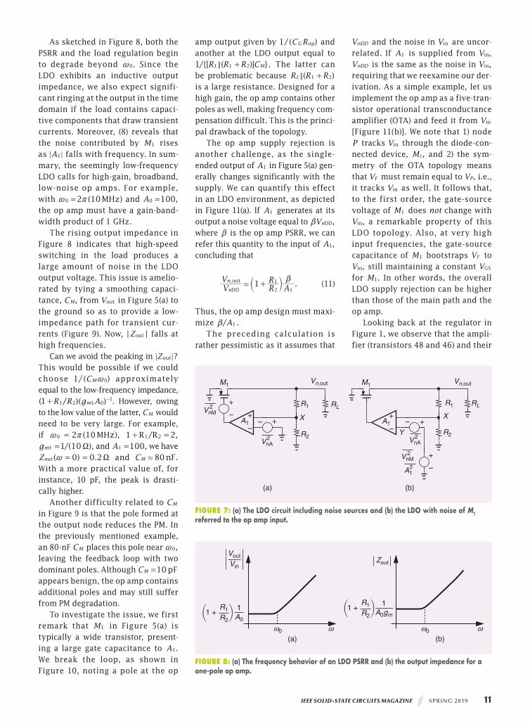
As sketched in Figure 8, both the PSRR and the load regulation begin to degrade beyond .0~ Since the LDO exhibits an inductive output impedance, we also expect signifi-cant ringing at the output in the time domain if the load contains capaci-tive components that draw transient currents. Moreover, (8) reveals that the noise contributed by M1 rises as A1; ; falls with frequency. In sum-mary, the seemingly low-frequency LDO calls for high-gain, broadband, low-noise op amps. For example, with ( )2 10MHz0~ r= and ,A 1000 = the op amp must have a gain-band-width product of 1 GHz.
The rising output impedance in Figure 8 indicates that high-speed switching in the load produces a large amount of noise in the LDO output voltage. This issue is amelio-rated by tying a smoothing capaci-tance, ,CM from Vout in Figure 5(a) to the ground so as to provide a low-impedance path for transient cur-rents (Figure 9). Now, | |Zout falls at high frequencies.
Can we avoid the peaking in ?Zout; ; This would be possible if we could choose /( )C1 M 0~ approximately equal to the low-frequency impedance, ( / )( ) .R R g A1 m1 2 1 0
1+ - However, owing to the low value of the latter, CM would need to be very large. For example, if ( ),2 10MHz0~ r= / ,R R1 21 2+ =
/( ),g 1 10m1 X= and ,A 1001 = we have ( ) .Z 0 0 2out ~ X= = and C 80 nF.M .
With a more practical value of, for instance, 10 pF, the peak is drasti-cally higher.
Another difficulty related to CM in Figure 9 is that the pole formed at the output node reduces the PM. In the previously mentioned example, an 80-nF CM places this pole near ,0~ leaving the feedback loop with two dominant poles. Although C 10 pFM = appears benign, the op amp contains additional poles and may still suffer from PM degradation.
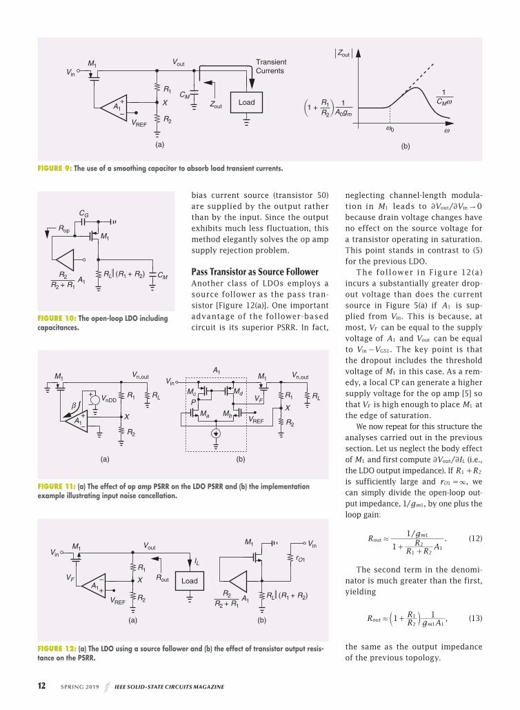
To investigate the issue, we first remark that M1 in Figure 5(a) is typically a wide transistor, present-ing a large gate capacitance to .A1 We break the loop, as shown in Figure 10, noting a pole at the op
amp output given by /( )C R1 G op and an other at the LDO output equal to /{[ ( )] } .R R R C1 L M1 2< + The latter can
be problematic because ( )R R RL 1 2< + is a large resistance. Designed for a high gain, the op amp contains other poles as well, making frequency com-pensation difficult. This is the princi-pal drawback of the topology.
The op amp supply rejection is another challenge, as the single-ended output of A1 in Figure 5(a) gen-erally changes significantly with the supply. We can quantify this effect in an LDO environment, as depicted in Figure 11(a). If A1 generates at its output a noise voltage equal to ,VnDDb where b is the op amp PSRR, we can refer this quantity to the input of ,A1 concluding that
.VV
RR
A1,
n
n
2
1
1DD
out.
b+c m (11)
Thus, the op amp design must maxi-mize / .A1b
The preceding calculation is rather pessimistic as it assumes that
VnDD and the noise in Vin are uncor-related. If A1 is supplied from ,Vin VnDD is the same as the noise in ,Vin requiring that we reexamine our der-ivation. As a simple example, let us implement the op amp as a five-tran-sistor operational transconductance amplifier (OTA) and feed it from Vin [Figure 11(b)]. We note that 1) node P tracks Vin through the diode-con-nected device, ,Mc and 2) the sym-metry of the OTA topology means that VF must remain equal to ,VP i.e., it tracks Vin as well. It follows that, to the first order, the gate-source voltage of M1 does not change with
,Vin a remarkable property of this LDO topology. Also, at very high input frequencies, the gate-source capacitance of M1 bootstraps VF to
,Vin still maintaining a constant VGS for .M1 In other words, the overall LDO supply rejection can be higher than those of the main path and the op amp.
Looking back at the regulator in Figure 1, we observe that the ampli-fier (transistors 48 and 46) and their
M1 M1
+
–VnM
2
A12
VnM2
VnA2 VnA
2
A1+
–A1
+
–+
+
–
–
R2R2
R1 R1
X X
RL RL
Vn,out Vn,out
Y
(b)(a)
– +
FIGURE 7: (a) The LDO circuit including noise sources and (b) the LDO with noise of M1 referred to the op amp input.
Vout
VinZout
1A0
R1
R21 +
1A0gm
R1
R21 +
ω0 ω0ω ω(a) (b)
FIGURE 8: (a) The frequency behavior of an LDO PSRR and (b) the output impedance for a one-pole op amp.
12 SPRING 20 19 IEEE SOLID-STATE CIRCUITS MAGAZINE
bias current source (transistor 50) are supplied by the output rather than by the input. Since the output exhibits much less fluctuation, this method elegantly solves the op amp supply rejection problem.
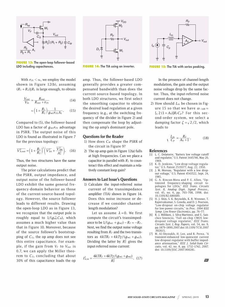
Pass Transistor as Source FollowerAnother class of LDOs employs a source follower as the pass tran-sistor [Figure 12(a)]. One important advantage of the follower-based circuit is its superior PSRR. In fact,
neglecting channel-length modula-tion in M1 leads to /V V 0out in "2 2 because drain voltage changes have no effect on the source voltage for a transistor operating in saturation. This point stands in contrast to (5) for the previous LDO.
The fol lower in Figure 12(a) incurs a substantially greater drop-out voltage than does the current source in Figure 5(a) if A1 is sup-plied from .Vin This is because, at most, VF can be equal to the supply voltage of A1 and Vout can be equal to .V V 1in GS- The key point is that the dropout includes the threshold voltage of M1 in this case. As a rem-edy, a local CP can generate a higher supply voltage for the op amp [5] so that VF is high enough to place M1 at the edge of saturation.
We now repeat for this structure the analyses carried out in the previous section. Let us neglect the body effect of M1 and first compute /V ILout2 2 (i.e., the LDO output impedance). If R R1 2+ is sufficiently large and ,rO1 3= we can simply divide the open-loop out-put impedance, / ,g1 m1 by one plus the loop gain:
/
.R
R RR A
g
1
1 m
1 2
21
1out .
++
(12)
The second term in the denomi-nator is much greater than the first, yielding
,R RR
g A1 1m2
1
1 1out . +c m (13)
the same as the output impedance of the previous topology.
CG
RopM1
CMR2
R2 + R1A1
RL (R1 + R2)
FIGURE 10: The open-loop LDO including capacitances.
M1 M1
Mc Md
Ma MbA1
+
–R2
R2
R1 R1
XXβ
+–
RL RLVnDD
Vin
A1Vn,out Vn,out
P VF
VREF
(b)(a)
FIGURE 11: (a) The effect of op amp PSRR on the LDO PSRR and (b) the implementation example illustrating input noise cancellation.
Load
M1M1
R2
R2 + R1A1
RL (R1 + R2)
Vin
rO1
A1+
–
R2
R1
X
ILVin
Rout
Vout
VF
VREF
(b)(a)
FIGURE 12: (a) The LDO using a source follower and (b) the effect of transistor output resis-tance on the PSRR.
Load
TransientCurrents
M1Vin
VREF
A1+
–R2
R1
X
Vout
Zout
Zout
1A0gm
R1
R21 +
1CMω
ω0 ω
(a) (b)
CM
FIGURE 9: The use of a smoothing capacitor to absorb load transient currents.
IEEE SOLID-STATE CIRCUITS MAGAZINE SPRING 20 19 13
With ,rO1 31 we employ the model shown in Figure 12(b), assuming ( )R R RL1 2 <+ is large enough, to obtain
VV
R rR
O1in
out
out
out=+
(14)
.RR
g r A1 1m O2
1
1 1 1. +c m (15)
Compared to (5), the follower-based LDO has a factor of g rm O1 1 advantage in PSRR. The output noise of this LDO is found as illustrated in Figure 7 for the previous topology:
.V RR V
AV1,n n
n2
2
12
2
12
2
out AM= + +c em o (16)
Thus, the two structures have the same output noise.
The prior calculations predict that the PSRR, output impedance, and output noise of the follower-based LDO exhibit the same general fre-quency-domain behavior as those of the current-source-based topol-ogy. However, the source follower leads to different results. Drawing the open-loop LDO as in Figure 13, we recognize that the output pole is roughly equal to /( ),g C1 m M1
1- which assumes a much higher value than that in Figure 10. Moreover, because of the source follower’s bootstrap-ping of ,CG the op amp does not see this entire capacitance. For exam-ple, if the gain from VF to Vout is 0.7, we can apply the Miller theo-rem to ,CG concluding that about 30% of this capacitance loads the op
amp. Thus, the follower-based LDO generally provides a greater com-pensated bandwidth than does the current-source-based topology. In both LDO structures, we first select the smoothing capacitor to obtain the desired load regulation at a given frequency (e.g., at the switching fre-quency of the divider in Figure 2) and then compensate the loop by adjust-ing the op amp’s dominant pole.
Questions for the Reader1) How does CM shape the PSRR of
the circuit in Figure 9?2) The op amp gain in Figure 12(a) falls
at high frequencies. Can we place a capacitor in parallel with R1 to coun-teract this effect and maintain a rela-tively constant loop gain?
Answers to Last Issue’s Questions1) Calculate the input-referred noise
current of the transimpedance amplifier (TIA) shown in Figure 14. Does this noise increase or de-crease if we consider channel-length modulation?
Let us assume .0m= We first compute the circuit’s transimped-ance to be /( ) .g g R R1 m m F F1 2 .+ - - Next, we find the output noise voltage resulting from RF and the two transis-tors as /( ).kTR kT g g4 4F m m1 2c+ + Dividing the latter by RF
2 gives the input-referred noise current:
/( ).I
RkTR kT g g4 4
,nF
F m m22
1 2in
c=
+ + (17)
In the presence of channel-length modulation, the gain and the output noise voltage drop by the same fac-tor. Thus, the input-referred noise current does not change.
2) How should Lin be chosen in Fig-ure 15 so that we have 3dB .~- [ ( )] ?A R C2 1 F p0+ For this sec-ond-order system, we select a damping factor / ,2 2g= which leads to
.CL
AR
1p
F
0
in =+
(18)
References[1] L. C. Delatorre, “Battery low voltage cutoff
and regulator,” U.S. Patent 3445746, May 20, 1969.
[2] K. D. Jenkins, “Low drop voltage regula-tor,” U.S. Patent 2519377, Aug. 22, 1950.
[3] J. M. Moreau, “Regulator with a low drop-out voltage,” U.S. Patent 4543522, Sept. 24, 1985.
[4] G. A. Rincon-Mora and P. E. Allen, “Op-timized frequency-shaping circuit to-pologies for LDOs,” IEEE Trans. Circuits Syst. II, Analog Digit. Signal Process., vol. 45, no. 6, pp. 703–708, 1998. doi: 10.1109/82.686689.
[5] H. J. Shin, S. K. Reynolds, K. R. Wrenner, T. Rajeevakumar, S. Gowda, and D. J. Pearson, “Low-dropout on-chip voltage regulator for low-power circuits,” in Proc. 1994 IEEE Symp. Low Power Electronics, pp. 76–77.
[6] R. J. Milliken, J. Silva-Martinez, and E. San-chez-Sinencio, “Full on-chip CMOS low-dropout voltage regulator,” IEEE Trans. Circuits Syst. I, Reg. Papers, vol. 54, no. 9, pp. 1879–1890, 2007. doi: 10.1109/TCSI.2007 .902615.
[7] M. Al-Shyoukh, H. Lee, and R. Perez, “A transient-enhanced low-quiescent current low-dropout regulator with buffer imped-ance attenuation,” IEEE J. Solid-State Cir-cuits, vol. 42, no. 8, pp. 1732–1742, 2007.doi: 10.1109/JSSC.2007.900281.
M1
R2
R2 + R1A1
RL (R1 + R2)
Vout
Rop
CM
CG
VF
FIGURE 13: The open-loop follower-based LDO including capacitances.
VDD
M2
RFVout
M1D1
FIGURE 14: The TIA using an inverter.
RF
Vout–
+A0
Lin
CpIin
FIGURE 15: The TIA with series peaking.