Embed Size (px)
Citation preview
PUBLIC
Doc. DS-090553 V1.6 WWW.CISSOID.COM 1 of 17
The Leader in High Temperature Semiconductor Solutions
CHT-ADC10 Datasheet Version: 1.6
8-Jul-14 (Last Modification Date)
High-Temperature Ultra-low-power 10-bit ADC
General Description The CHT-ADC10 is a high-temperature, ultra-low-power, highly stable analog-to-digital converter. This successive approxi-mation ADC is based on an R-2R network and features 10 bits of resolution and a strictly monotonic characteristic from -55°C up to +225°C. An optional internal clock generator is included to provide stand-alone operation. It includes Sample&Hold and µP interface with possibility of serial data transfer. Both parallel and serial inter-faces can be used simultaneously. A spe-cial control line allows for doubling the fre-quency of the internal clock generator for reduced throughput time. The maximum sampling rate is 25kS/s. Several input ranges are available from -15V up to +10V. It only requires a +5V supply and an exter-nal +5V reference. The CHT-ADC10 is latch-up free and the fabrication technology guarantees a high reliability at extreme temperatures.
Features 10 bit-resolution with optional internal
clock, Sample/Hold, µC interface with
parallel or serial data transfer
Up to 25kS/s
+5V power supply only
Low total supply current ( <250 µA)
Operational from -55 to +225°C with
very low drift
Validated at 225°C for 20000 hours (and
still on-going)
Available in die, CDIL28 and CSOIC28
Applications Oil&Gas, Industrial, Automotive, Aero-
nautics & Aerospace
Electric Power Conversion
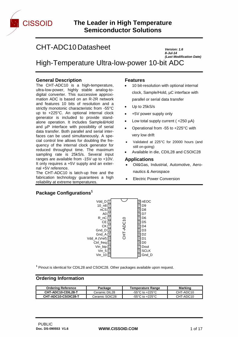
Package Configurations1
Vdd_D
10_n8
nCS
A0
R_nC
CE
CK
Gnd_D
Gnd_A
Vdd_A (Vref)
Ctrl_freq
Vin_bip
Vin_5
Vin_10
nEOC
D9
D8
D7
D6
D5
D4
D3
D2
D1
D0
Dout
SCLK
Gnd_D
1
2
3
4
5
6
7
8
9
10
11
12
13
14
28
27
26
25
24
23
22
21
20
19
18
17
16
15
CH
T-A
DC
10
1 Pinout is identical for CDIL28 and CSOIC28. Other packages available upon request.
Ordering Information
Ordering Reference Package Temperature Range Marking
CHT-ADC10-CDIL28-T Ceramic DIL28 -55°C to +225°C CHT-ADC10
CHT-ADC10-CSOIC28-T Ceramic SOIC28 -55°C to +225°C CHT-ADC10
8-Jul-14 Contact : Gonzalo Picún (+32-10-489214)Jul. 14 CHT-ADC10 - DATASHEET
(Last Modification Date)
PUBLIC
Doc. DS-090553 V1.6 WWW.CISSOID.COM 2 of 17
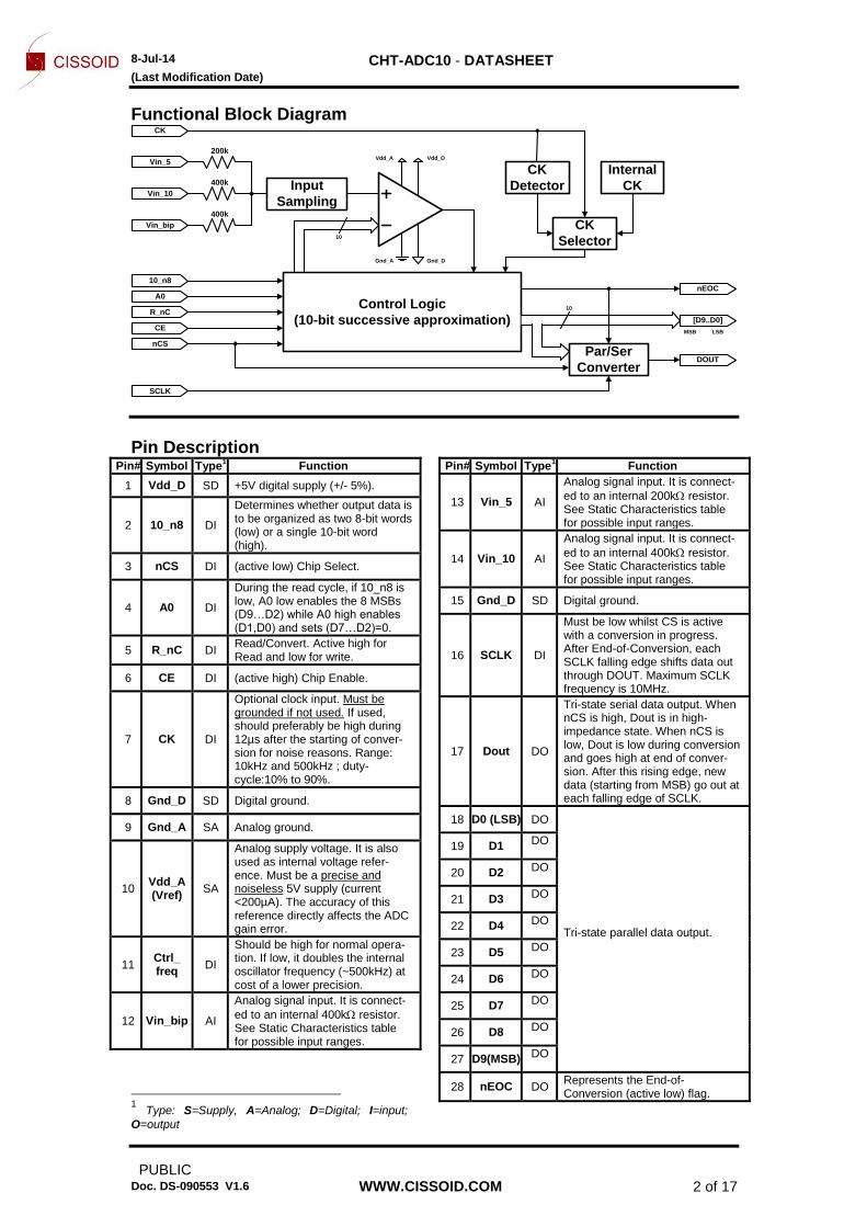
Functional Block Diagram
Input
Sampling
400k
400k
200k
Control Logic
(10-bit successive approximation)
Gnd_DGnd_A
Vdd_DVdd_A
Par/Ser
Converter
Vin_5
Vin_10
Vin_bip
10_n8
10
10
nEOC
DOUT
CK
Detector
Internal
CK
CK
Selector
CK
SCLK
[D9..D0]
MSB LSB
A0
R_nC
CE
nCS
Pin Description Pin# Symbol Type
1 Function
1 Vdd_D SD +5V digital supply (+/- 5%).
2 10_n8 DI
Determines whether output data is to be organized as two 8-bit words (low) or a single 10-bit word (high).
3 nCS DI (active low) Chip Select.
4 A0 DI
During the read cycle, if 10_n8 is low, A0 low enables the 8 MSBs (D9…D2) while A0 high enables (D1,D0) and sets (D7…D2)=0.
5 R_nC DI Read/Convert. Active high for Read and low for write.
6 CE DI (active high) Chip Enable.
7 CK DI
Optional clock input. Must be grounded if not used. If used, should preferably be high during 12µs after the starting of conver-sion for noise reasons. Range: 10kHz and 500kHz ; duty-cycle:10% to 90%.
8 Gnd_D SD Digital ground.
9 Gnd_A SA Analog ground.
10 Vdd_A (Vref)
SA
Analog supply voltage. It is also used as internal voltage refer-ence. Must be a precise and noiseless 5V supply (current <200µA). The accuracy of this reference directly affects the ADC gain error.
11 Ctrl_ freq
DI
Should be high for normal opera-tion. If low, it doubles the internal oscillator frequency (~500kHz) at cost of a lower precision.
12 Vin_bip AI
Analog signal input. It is connect-
ed to an internal 400k resistor. See Static Characteristics table for possible input ranges.
1 Type: S=Supply, A=Analog; D=Digital; I=input;
O=output
Pin# Symbol Type1
Function
13 Vin_5 AI
Analog signal input. It is connect-
ed to an internal 200k resistor. See Static Characteristics table for possible input ranges.
14 Vin_10 AI
Analog signal input. It is connect-
ed to an internal 400k resistor. See Static Characteristics table for possible input ranges.
15 Gnd_D SD Digital ground.
16 SCLK DI
Must be low whilst CS is active with a conversion in progress. After End-of-Conversion, each SCLK falling edge shifts data out through DOUT. Maximum SCLK frequency is 10MHz.
17 Dout DO
Tri-state serial data output. When nCS is high, Dout is in high-impedance state. When nCS is low, Dout is low during conversion and goes high at end of conver-sion. After this rising edge, new data (starting from MSB) go out at each falling edge of SCLK.
18 D0 (LSB) DO
Tri-state parallel data output.
19 D1 DO
20 D2 DO
21 D3 DO
22 D4 DO
23 D5 DO
24 D6 DO
25 D7 DO
26 D8 DO
27 D9(MSB) DO
28 nEOC DO Represents the End-of-Conversion (active low) flag.
8-Jul-14 Contact : Gonzalo Picún (+32-10-489214)Jul. 14 CHT-ADC10 - DATASHEET
(Last Modification Date)
PUBLIC
Doc. DS-090553 V1.6 WWW.CISSOID.COM 3 of 17
Absolute Maximum Ratings Supply Voltage VDD to GND -0.5 to 5.5V Voltage on any Pin to GND -0.5 to VDD+0.5V ESD Rating (expected) Human Body Model (expected) <1kV
Operating Conditions Supply Voltage VDD to GND 5V ± 5% Junction temperature -55°C to +225°C
Stresses above those listed in “Absolute Maximum Ratings” may cause permanent damage to the device. This is a stress only rating and operation of the device at these or any other conditions above those indicated in the operational sections of this specification is not implied. Frequent or extended exposure to absolute maximum rating conditions or above may affect device reliability.
Electrical Characteristics Unless otherwise stated: VDDD=5V5%, Tj=25°C, output data rate=10 kS/s. Bold figures indi-cate values over the whole temperature range (-55°C < Tj <225°C).
Parameter Condition Min Typ Max Units Digital Supply voltage (VDDD)
4.75 5.00 5.25 V
Analog Supply voltage (VDDA)
Used as internal voltage reference 5 V
Current consumption (analog part)
-55°C 225°C
134 164
µA
Current consumption (digital part)
Using external CK 55 µA
Using internal CK 70 µA
Static characteristics Unless otherwise stated: VDDD=5V5%, Tj=25°C. Bold figures indicate values over the whole temperature range (-55°C < Tj <225°C). Units are referred to 10 bit word. Selected input range=0 to 5V.
Parameter Condition Min Typ Max Units Resolution 10 Bits
DNL1 1.3 1.5 LSB
INL1 1.3 1.5 LSB
Missing code 0 1
Monotonicity OK
Offset2
17 LSB
1
Gain Error2
1.5 %
Temperature Drift (d/dT°) - Offset - Gain Error
-0.023 -19
LSB/°C ppm/°C
Selectable Analog Input Ranges
Vin_5 Vin_10 Vin_bip
gndA in gndA
in gndA gndA
in in gndA
in in in
in in vddA
in gndA vddA
gndA in vddA
in vddA vddA
vddA in gndA
vddA in vddA
0
0
0
0
-1.67
-2.5
-5
-5
-10
-15
10
5
3.33
2.5
1.67
2.5
5
0
0
-5
V
Input Impedance - Sample phase - Hold phase
For [0…5V] range. Can change up to a factor of 2 for other ranges.
144 288
200 400
245 490
k
1 Value extracted with code density method, using 200kHz external clock.
2 For [0…5]V range, DAC transfer function is: D=Offset+(1024/5)*A*(1-(Gain Error/100))
8-Jul-14 Contact : Gonzalo Picún (+32-10-489214)Jul. 14 CHT-ADC10 - DATASHEET
(Last Modification Date)
PUBLIC
Doc. DS-090553 V1.6 WWW.CISSOID.COM 4 of 17
Timing Characteristics Unless otherwise stated: VDDD=5V5%, Tj=25°C, output data rate=10 kS/s. Bold figures indi-cate values over the whole temperature range (-55°C < Tj <225°C).
Parameter Condition Min Typ Max Units External CK frequency Duty cycle between 10% and 90% 10 250 500 kHz
Output data rate 0.8 16 25 kS/s
Data Output Delay (clock edge to valid data)
TBD ns
Sampling time before Hold
When conversion starts, actual sampling occurs after this sam-pling time.
8 10 12 µs
Data latency Occurs when S/H goes to hold state.
13 cycles
Conversion time (tC) Cfr figure 12 for timing diagram 58 µs
NEOC delay from CE (tDSC)
Cfr figure 12 for timing diagram 15 ns
CE pulse width (tHEC) Cfr figure 12 for timing diagram 40 ns
nCS to CE high setup time (tSSC)
Cfr figure 12 for timing diagram 40 ns
nCS to CE high hold time (tHSC)
Cfr figure 12 for timing diagram 40 ns
R_nC to CE high setup time (tSRC)
Cfr figure 12 for timing diagram 40 ns
R_nC to CE high hold time (tHRC)
Cfr figure 12 for timing diagram 40 ns
A0 to CE high setup time (tSAC)
Cfr figure 12 for timing diagram 5 ns
A0 to CE high hold time (tHAC)
Cfr figure 12 for timing diagram 40 ns
Access time (tDD) Cfr figure 13 for timing diagram 9 ns
Data valid to CE low hold time (tHD)
Cfr figure 13 for timing diagram 6 ns
Output float after CE faling edge (tHL)
Cfr figure 13 for timing diagram 11 ns
nCS to CE high setup time (tSSR)
Cfr figure 13 for timing diagram 40 ns
R_nC to CE high setup time (tSRR)
Cfr figure 13 for timing diagram 40 ns
A0 to CE high setup time (tSAR)
Cfr figure 13 for timing diagram 40 ns
nCS to CE low hold time (tHSR)
Cfr figure 13 for timing diagram 0 ns
R_nC to CE low hold time (tHRR)
Cfr figure 13 for timing diagram 0 ns
A0 to CE low hold time (tHAR)
Cfr figure 13 for timing diagram 40 ns
D<9..0> delay from SCLK falling edge
Cfr figure 15 for timing diagram 4 10 25 ns
8-Jul-14 Contact : Gonzalo Picún (+32-10-489214)Jul. 14 CHT-ADC10 - DATASHEET
(Last Modification Date)
PUBLIC
Doc. DS-090553 V1.6 WWW.CISSOID.COM 5 of 17
AC Characteristics Unless otherwise stated: VDDD=5V5%, Tj=25°C, 13.2kSamples/s, analog input of 4.9Vpp at 1kHz; VDDD=5V
Parameter Condition Min Typ Max Units Signal to Noise and distor-tion ratio (ENOB)
Tj=25°C ; external CK 200kHz Tj=225°C ; external CK 200kHz Tj=25°C ; internal CK Tj=225°C ; internal CK
9.1 - - -
9.47 9.35 9.30 9.13
9.6 - - -
dB
ENOB
Tj=25°C; external CK 200kHz -Vddd=4.75V -Vddd=5.00 -Vddd=5.25V
9.31 9.47 9.55
dB
Analog to Digital transfer function can be generalized to all input ranges defining: D= Digital value A= Analog input value Amin=lowest value of selected analog input range from Amax=highest value of selected analog input range from Offset= value of D when A=Amin. Offset value is independent of range. GE=Gain-Error (in %). GE value is independent of range.
D=Offset+(A-Amin)*(1024/(Amax-Amin))*(1-GE/100).
Equation 1
8-Jul-14 Contact : Gonzalo Picún (+32-10-489214)Jul. 14 CHT-ADC10 - DATASHEET
(Last Modification Date)
PUBLIC
Doc. DS-090553 V1.6 WWW.CISSOID.COM 6 of 17
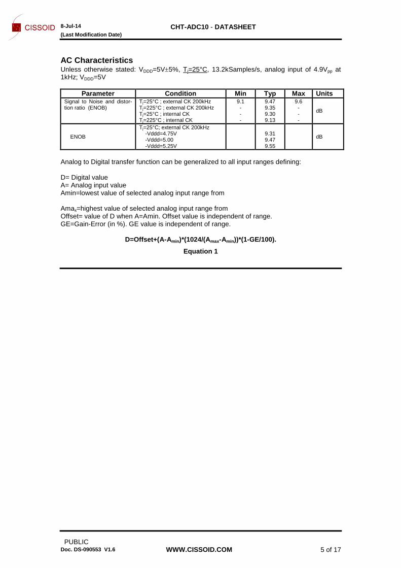
Typical Performance Characteristics Typical DNL Characteristics (using external clock at 200kHz)
-1
-0.5
0
0.5
1
1.5
2
2.5
3
0 256 512 768 1024
DNL [LSB] vs. digital code; -55°C – (external CK)
-1
-0.5
0
0.5
1
1.5
2
2.5
3
0 256 512 768 1024
DNL [LSB] vs. digital code; 25°C – (external CK)
-1
-0.5
0
0.5
1
1.5
2
2.5
3
0 256 512 768 1024
DNL [LSB] vs. digital code; 225°C – (external CK)
-1
-0.5
0
0.5
1
1.5
2
2.5
3
0 256 512 768 1024
DNL [LSB] vs. digital code; 300°C – (external CK)
Figure 1
8-Jul-14 Contact : Gonzalo Picún (+32-10-489214)Jul. 14 CHT-ADC10 - DATASHEET
(Last Modification Date)
PUBLIC
Doc. DS-090553 V1.6 WWW.CISSOID.COM 7 of 17
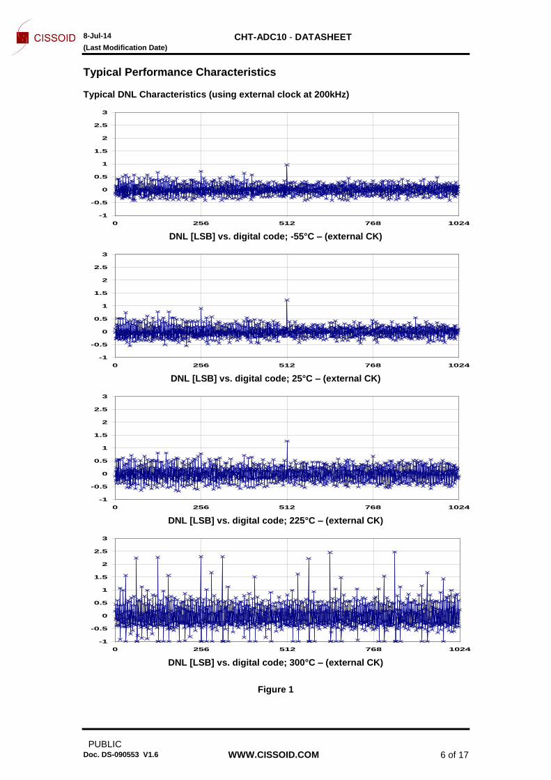
Typical INL Characteristics (using external clock at 200kHz)
-2
-1.5
-1
-0.5
0
0.5
1
1.5
2
0 256 512 768 1024
INL [LSB] vs. digital code; -55°C – (external CK)
-2
-1.5
-1
-0.5
0
0.5
1
1.5
2
0 256 512 768 1024
INL [LSB] vs. digital code; 25°C – (external CK)
-2
-1.5
-1
-0.5
0
0.5
1
1.5
2
0 256 512 768 1024
INL [LSB] vs. digital code; 225°C – (external CK)
-4
-3.5
-3
-2.5
-2
-1.5
-1
-0.5
0
0.5
1
1.5
2
2.5
3
0 256 512 768 1024
INL [LSB] vs. digital code; 300°C – (external CK)
Figure 2
8-Jul-14 Contact : Gonzalo Picún (+32-10-489214)Jul. 14 CHT-ADC10 - DATASHEET
(Last Modification Date)
PUBLIC
Doc. DS-090553 V1.6 WWW.CISSOID.COM 8 of 17
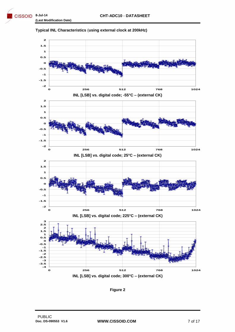
Typical DNL & INL Characteristics (using internal clock)
-1
-0.5
0
0.5
1
1.5
2
2.5
3
0 256 512 768 1024
DNL [LSB] vs. digital code; 25°C – (internal CK)
-2
-1.5
-1
-0.5
0
0.5
1
1.5
2
0 256 512 768 1024
INL [LSB] vs. digital code; 25°C – (internal CK)
-1
-0.5
0
0.5
1
1.5
2
2.5
3
0 256 512 768 1024
DNL [LSB] vs. digital code; 225°C – (internal CK)
-2
-1.5
-1
-0.5
0
0.5
1
1.5
2
0 256 512 768 1024
INL [LSB] vs. digital code; 225°C – (internal CK)
Figure 3
8-Jul-14 Contact : Gonzalo Picún (+32-10-489214)Jul. 14 CHT-ADC10 - DATASHEET
(Last Modification Date)
PUBLIC
Doc. DS-090553 V1.6 WWW.CISSOID.COM 9 of 17
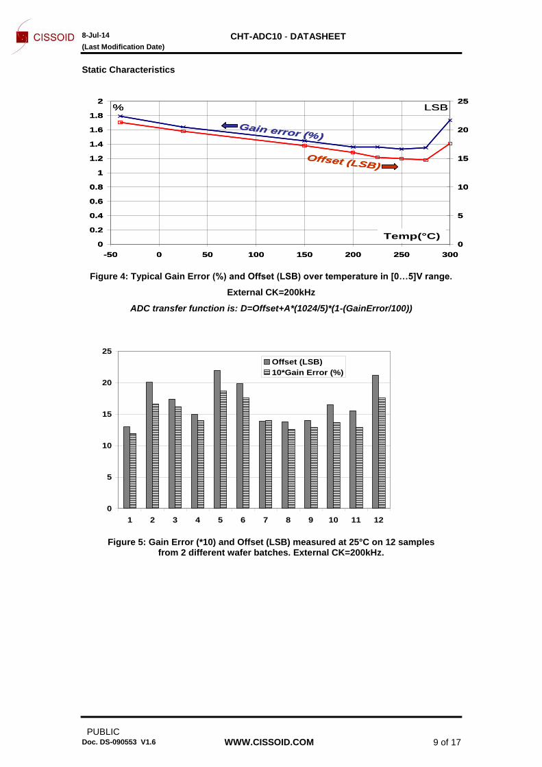
Static Characteristics
0
0.2
0.4
0.6
0.8
1
1.2
1.4
1.6
1.8
2
-50 0 50 100 150 200 250 300
0
5
10
15
20
25
Gain error (%)
Offset (LSB)
Temp(°C)
% LSB
0
0.2
0.4
0.6
0.8
1
1.2
1.4
1.6
1.8
2
-50 0 50 100 150 200 250 300
0
5
10
15
20
25
Gain error (%)
Offset (LSB)
Temp(°C)
% LSB
Figure 4: Typical Gain Error (%) and Offset (LSB) over temperature in [0…5]V range.
External CK=200kHz
ADC transfer function is: D=Offset+A*(1024/5)*(1-(GainError/100))
0
5
10
15
20
25
1 2 3 4 5 6 7 8 9 10 11 12
Offset (LSB)
10*Gain Error (%)
Figure 5: Gain Error (*10) and Offset (LSB) measured at 25°C on 12 samples from 2 different wafer batches. External CK=200kHz.
8-Jul-14 Contact : Gonzalo Picún (+32-10-489214)Jul. 14 CHT-ADC10 - DATASHEET
(Last Modification Date)
PUBLIC
Doc. DS-090553 V1.6 WWW.CISSOID.COM 10 of 17
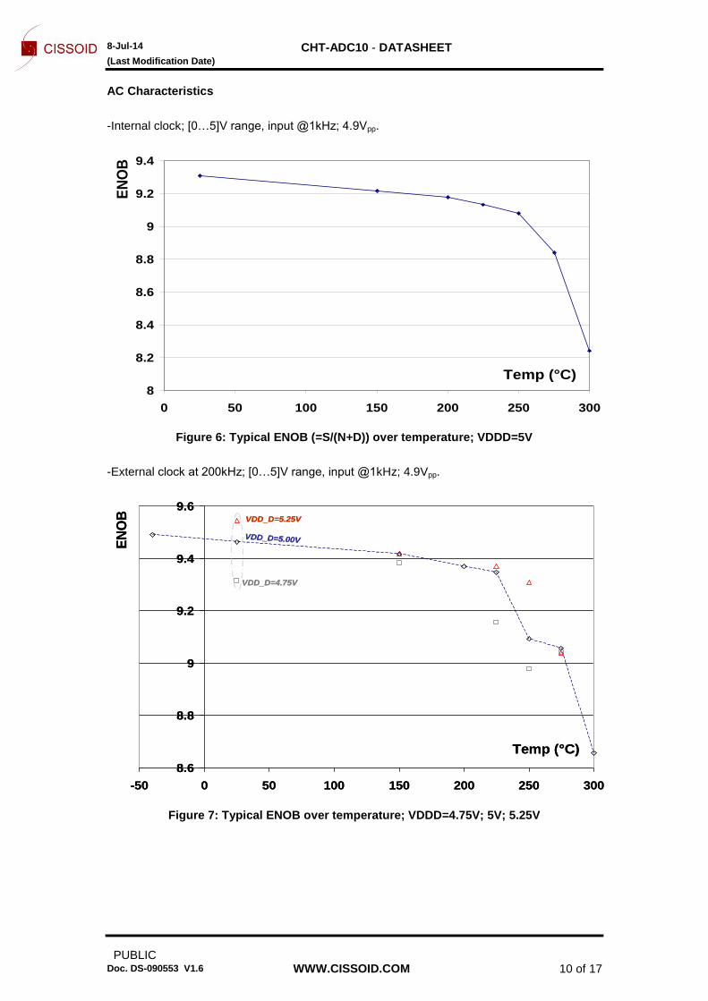
AC Characteristics
-Internal clock; [0…5]V range, input @1kHz; 4.9Vpp.
8
8.2
8.4
8.6
8.8
9
9.2
9.4
0 50 100 150 200 250 300
Temp (°C)
EN
OB
Figure 6: Typical ENOB (=S/(N+D)) over temperature; VDDD=5V
-External clock at 200kHz; [0…5]V range, input @1kHz; 4.9Vpp.
8.6
8.8
9
9.2
9.4
9.6
-50 0 50 100 150 200 250 300
Temp (°C)
EN
OB
VDD_D=5.00V
VDD_D=5.25V
VDD_D=4.75V
8.6
8.8
9
9.2
9.4
9.6
-50 0 50 100 150 200 250 300
Temp (°C)
EN
OB
VDD_D=5.00V
VDD_D=5.25V
VDD_D=4.75V
Figure 7: Typical ENOB over temperature; VDDD=4.75V; 5V; 5.25V
8-Jul-14 Contact : Gonzalo Picún (+32-10-489214)Jul. 14 CHT-ADC10 - DATASHEET
(Last Modification Date)
PUBLIC
Doc. DS-090553 V1.6 WWW.CISSOID.COM 11 of 17
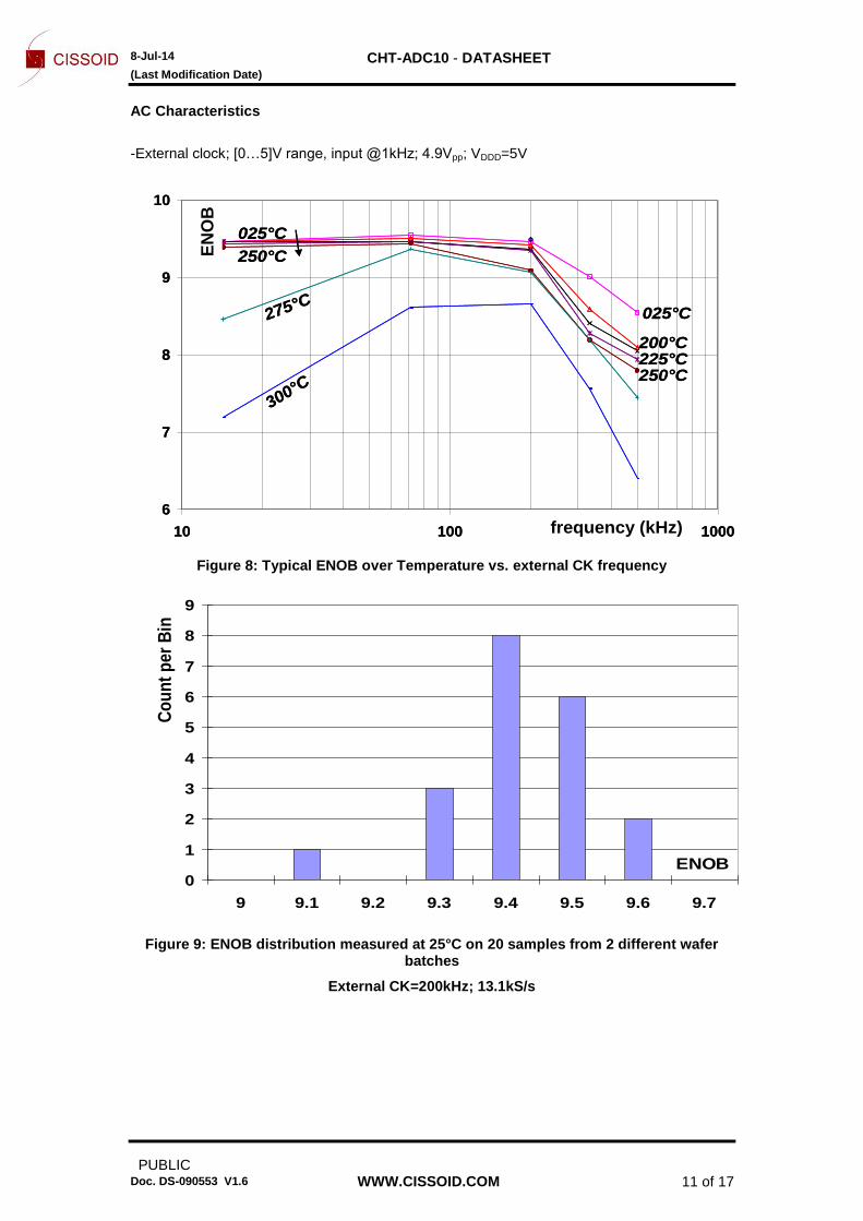
AC Characteristics
-External clock; [0…5]V range, input @1kHz; 4.9Vpp; VDDD=5V
6
7
8
9
10
10 100 1000frequency (kHz)
EN
OB
300°C
275°C
250°C225°C200°C
025°C
250°C
025°C
6
7
8
9
10
10 100 1000frequency (kHz)
EN
OB
300°C
275°C
250°C225°C200°C
025°C
250°C
025°C
Figure 8: Typical ENOB over Temperature vs. external CK frequency
0
1
2
3
4
5
6
7
8
9
9 9.1 9.2 9.3 9.4 9.5 9.6 9.7
ENOB
Co
un
t p
er
Bin
Figure 9: ENOB distribution measured at 25°C on 20 samples from 2 different wafer batches
External CK=200kHz; 13.1kS/s
8-Jul-14 Contact : Gonzalo Picún (+32-10-489214)Jul. 14 CHT-ADC10 - DATASHEET
(Last Modification Date)
PUBLIC
Doc. DS-090553 V1.6 WWW.CISSOID.COM 12 of 17
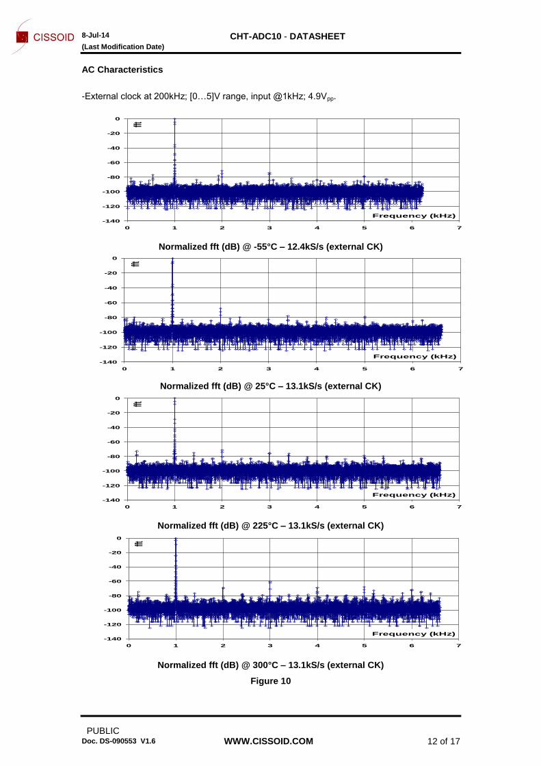
AC Characteristics
-External clock at 200kHz; [0…5]V range, input @1kHz; 4.9Vpp.
-140
-120
-100
-80
-60
-40
-20
0
0 1 2 3 4 5 6 7
Frequency (kHz)
fft
Normalized fft (dB) @ -55°C – 12.4kS/s (external CK)
-140
-120
-100
-80
-60
-40
-20
0
0 1 2 3 4 5 6 7
Frequency (kHz)
fft
Normalized fft (dB) @ 25°C – 13.1kS/s (external CK)
-140
-120
-100
-80
-60
-40
-20
0
0 1 2 3 4 5 6 7
Frequency (kHz)
fft
Normalized fft (dB) @ 225°C – 13.1kS/s (external CK)
-140
-120
-100
-80
-60
-40
-20
0
0 1 2 3 4 5 6 7
Frequency (kHz)
fft
Normalized fft (dB) @ 300°C – 13.1kS/s (external CK)
Figure 10
8-Jul-14 Contact : Gonzalo Picún (+32-10-489214)Jul. 14 CHT-ADC10 - DATASHEET
(Last Modification Date)
PUBLIC
Doc. DS-090553 V1.6 WWW.CISSOID.COM 13 of 17
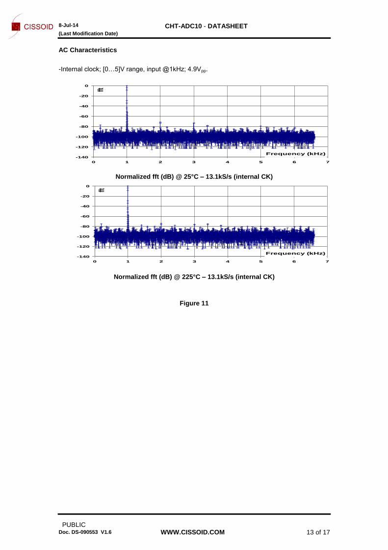
AC Characteristics
-Internal clock; [0…5]V range, input @1kHz; 4.9Vpp.
-140
-120
-100
-80
-60
-40
-20
0
0 1 2 3 4 5 6 7
Frequency (kHz)
fft
Normalized fft (dB) @ 25°C – 13.1kS/s (internal CK)
-140
-120
-100
-80
-60
-40
-20
0
0 1 2 3 4 5 6 7
Frequency (kHz)
fft
Normalized fft (dB) @ 225°C – 13.1kS/s (internal CK)
Figure 11
8-Jul-14 Contact : Gonzalo Picún (+32-10-489214)Jul. 14 CHT-ADC10 - DATASHEET
(Last Modification Date)
PUBLIC
Doc. DS-090553 V1.6 WWW.CISSOID.COM 14 of 17
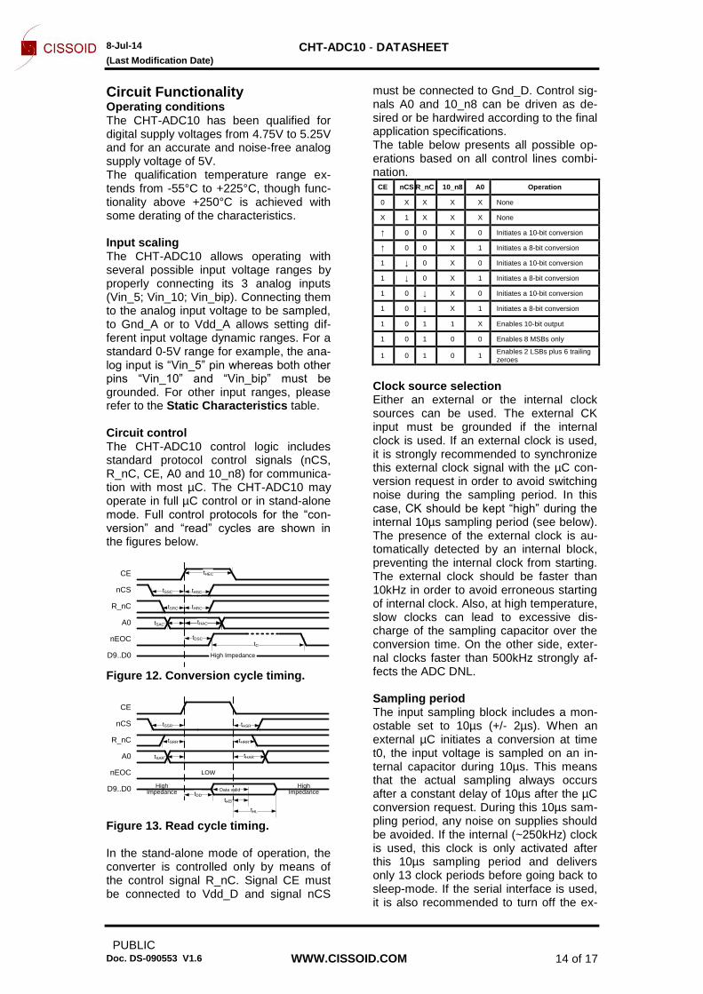
Circuit Functionality Operating conditions The CHT-ADC10 has been qualified for digital supply voltages from 4.75V to 5.25V and for an accurate and noise-free analog supply voltage of 5V. The qualification temperature range ex-tends from -55°C to +225°C, though func-tionality above +250°C is achieved with some derating of the characteristics. Input scaling The CHT-ADC10 allows operating with several possible input voltage ranges by properly connecting its 3 analog inputs (Vin_5; Vin_10; Vin_bip). Connecting them to the analog input voltage to be sampled, to Gnd_A or to Vdd_A allows setting dif-ferent input voltage dynamic ranges. For a standard 0-5V range for example, the ana-log input is “Vin_5” pin whereas both other pins “Vin_10” and “Vin_bip” must be grounded. For other input ranges, please refer to the Static Characteristics table. Circuit control The CHT-ADC10 control logic includes standard protocol control signals (nCS, R_nC, CE, A0 and 10_n8) for communica-tion with most µC. The CHT-ADC10 may operate in full µC control or in stand-alone mode. Full control protocols for the “con-version” and “read” cycles are shown in the figures below.
A0
R_nC
nEOC
CE
tSSCnCS
High ImpedanceD9..D0
tHEC
tHSC
tSRC tHRC
tSAC tHAC
tDSC
tC
Figure 12. Conversion cycle timing.
tSSR
HighImpedance
tHSR
tSRR tHRR
tSAR tHAR
HighImpedanceData valid
tHD
tDD
tHL
LOW
A0
R_nC
nEOC
CE
nCS
D9..D0
Figure 13. Read cycle timing. In the stand-alone mode of operation, the converter is controlled only by means of the control signal R_nC. Signal CE must be connected to Vdd_D and signal nCS
must be connected to Gnd_D. Control sig-nals A0 and 10_n8 can be driven as de-sired or be hardwired according to the final application specifications. The table below presents all possible op-erations based on all control lines combi-nation.
CE nCS R_nC 10_n8 A0 Operation
0 X X X X None
X 1 X X X None
↑ 0 0 X 0 Initiates a 10-bit conversion
↑ 0 0 X 1 Initiates a 8-bit conversion
1 ↓ 0 X 0 Initiates a 10-bit conversion
1 ↓ 0 X 1 Initiates a 8-bit conversion
1 0 ↓ X 0 Initiates a 10-bit conversion
1 0 ↓ X 1 Initiates a 8-bit conversion
1 0 1 1 X Enables 10-bit output
1 0 1 0 0 Enables 8 MSBs only
1 0 1 0 1 Enables 2 LSBs plus 6 trailing zeroes
Clock source selection Either an external or the internal clock sources can be used. The external CK input must be grounded if the internal clock is used. If an external clock is used, it is strongly recommended to synchronize this external clock signal with the µC con-version request in order to avoid switching noise during the sampling period. In this case, CK should be kept “high” during the internal 10µs sampling period (see below). The presence of the external clock is au-tomatically detected by an internal block, preventing the internal clock from starting. The external clock should be faster than 10kHz in order to avoid erroneous starting of internal clock. Also, at high temperature, slow clocks can lead to excessive dis-charge of the sampling capacitor over the conversion time. On the other side, exter-nal clocks faster than 500kHz strongly af-fects the ADC DNL. Sampling period The input sampling block includes a mon-ostable set to 10µs (+/- 2µs). When an external µC initiates a conversion at time t0, the input voltage is sampled on an in-ternal capacitor during 10µs. This means that the actual sampling always occurs after a constant delay of 10µs after the µC conversion request. During this 10µs sam-pling period, any noise on supplies should be avoided. If the internal (~250kHz) clock is used, this clock is only activated after this 10µs sampling period and delivers only 13 clock periods before going back to sleep-mode. If the serial interface is used, it is also recommended to turn off the ex-
8-Jul-14 Contact : Gonzalo Picún (+32-10-489214)Jul. 14 CHT-ADC10 - DATASHEET
(Last Modification Date)
PUBLIC
Doc. DS-090553 V1.6 WWW.CISSOID.COM 15 of 17
ternal serial clock SCLK during the sam-pling and conversion periods. During the 10µs sampling period, the “in-put sampling” block sets its input to 2.5V. This means that input impedance during
this time period is about 200k for [0-5V] input range setting. After the 10µs sam-pling period, the input sampling block can be considered as an open circuit, leading
to an input impedance of about 400k. Absolute impedance values can change up to 30% over temperature and from lot to lot. This is not critical for the ADC as it is based on ratios between resistors and not on their absolute values. Conversion cycle A conversion cycle is started whenever the following logic condition occurs: (CE=HIGH)&(nCS=LOW)&(R_nC=LOW)
Conversion start is asserted by the rising edge of the condition above. Once the condition is set, conversion is not restarted provided that there is no new rising edge of the condition. Depending on the value of A0 at the mo-ment where the conversion start condition is asserted, either a 10bit (A0=LOW) or an 8bit (A0=HIGH) conversion cycle is exe-cuted. If an 8-bit conversion cycle is per-formed, the result is present in the 8 MSBs, with the remaining two LSBs set to zero. The value of A0 is latched with the rising edge of the conversion start condi-tion. During the conversion cycle, nEOC is HIGH and the parallel output bus is set to high-impedance state. Depending on the value of nCS, the serial data output can be at LOW (nCS=LOW) or high-impedance (nCS=HIGH) state. Once the conversion cycle has finished nEOC returns to LOW and the conversion result is stored in the internal parallel and serial registers. Reading output data Once the conversion cycle ends, data can be read out through either any or both parallel and serial ports. Both parallel and serial output interfaces are always active together and can be used simultaneously. To use the parallel port control signal 10_n8 must be accordingly set. If 10_n8 is HIGH, all 10 output lines are enabled at the same time allowing full data word transfer to a bus of at least 10bits. In this case A0 has no influence on the read da-ta. If 10_n8 is LOW, output data is pre-sented as a two 8-bit words. In this case
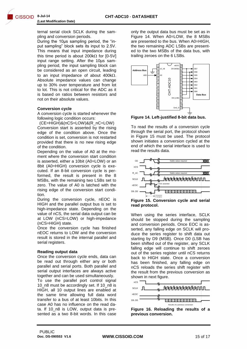
only the output data bus must be set as in Figure 14. When A0=LOW, the 8 MSBs are presented to the bus. When A0=HIGH, the two remaining ADC LSBs are present-ed to the two MSBs of the data bus, with trailing zeroes on the 6 LSBs.
1
2
3
4
5
6
7
8
9
10
11
12
13
14
28
27
26
25
24
23
22
21
20
19
18
17
16
15
CH
T-A
DC
10
D9 (MSB)
D0 (LSB)
Gnd_D
10_n8
A0
nEOC
Address Bus
Data Bus
AB0
DB7
DB6
DB5
DB4
DB3
DB2
DB1
DB0
Figure 14. Left-justified 8-bit data bus. To read the results of a conversion cycle through the serial port, the protocol shown in Figure 15 must be used. The protocol shown initiates a conversion cycled at the end of which the serial interface is used to read the results data.
R_nC
nEOC
D9..D0 D9 D8 D7 D6 D5 D4 D3 D2 D1 D0
1 4 7 10
Conversion
in progress
Stable values required
Stable values required
SCLK
CE
nCS
EOC asserted
Figure 15. Conversion cycle and serial read protocol. When using the series interface, SCLK should be stopped during the sampling and conversion periods. Once EOC is as-serted, any falling edge on SCLK will pro-duce the series register to shift data out starting by D9 (MSB). Once D0 (LSB has been shifted out of the register, any SCLK falling edge will continue to shift zeroes out of the series register until nCS returns back to HIGH state. Once a conversion has been finished, any falling edge on nCS reloads the series shift register with the result from the previous conversion as shown in next figure.
nEOC
D9..D0 D9 D8 D7 D6 D5 D4 D3 D2 D1 D0
1 4 7 10
SCLK
nCS
Results of a previous conversion Figure 16. Reloading the results of a previous conversion.
8-Jul-14 Contact : Gonzalo Picún (+32-10-489214)Jul. 14 CHT-ADC10 - DATASHEET
(Last Modification Date)
PUBLIC
Doc. DS-090553 V1.6 WWW.CISSOID.COM 16 of 17
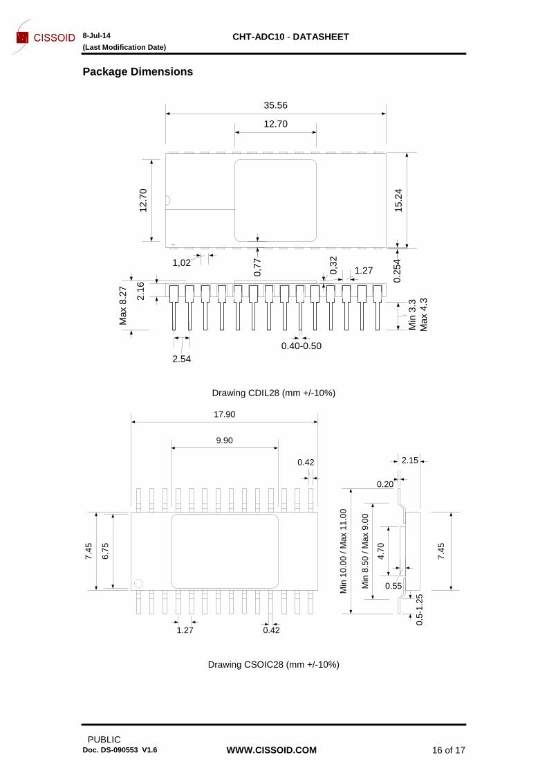
Package Dimensions
0,7
7
12.70
1.27
0.40-0.50
Min
3.3
Ma
x 4
.3
0,3
2
Ma
x 8
.27
2.54
35.56
12
.70
2.1
6
1,02
15
.24
0.2
54
Drawing CDIL28 (mm +/-10%)
4.7
0
17.90
9.90
6.7
5
7.4
5
1.27 0.42
0.42
7.4
5
0.20
4.7
0
0.55
2.15
Min
8.5
0 / M
ax 9
.00
0.5
-1.2
5
Min
10.0
0 / M
ax 1
1.0
0
Drawing CSOIC28 (mm +/-10%)
8-Jul-14 Contact : Gonzalo Picún (+32-10-489214)Jul. 14 CHT-ADC10 - DATASHEET
(Last Modification Date)
PUBLIC
Doc. DS-090553 V1.6 WWW.CISSOID.COM 17 of 17
Contact & Ordering CISSOID S.A.
Headquarters and contact EMEA:
CISSOID S.A. – Rue Francqui, 3 – 1435 Mont Saint Guibert - Belgium T : +32 10 48 92 10 - F: +32 10 88 98 75 Email: [email protected]
Sales Representatives:
Visit our website: http://www.cissoid.com
Disclaimer Neither CISSOID, nor any of its directors, employees or affiliates make any representations or extend any warranties of any kind, either express or implied, including but not limited to warranties of merchantability, fitness for a particular purpose, and the absence of latent or other defects, whether or not discoverable. In no event shall CISSOID, its di-rectors, employees and affiliates be liable for direct, indirect, special, incidental or consequential damages of any kind arising out of the use of its circuits and their documentation, even if they have been advised of the possibility of such a damage. The circuits are provided “as is”. CISSOID has no obligation to provide maintenance, support, updates, or modifications.