Embed Size (px)
Citation preview

1
Based on slides © McGraw-HillAdditional material © 2013 Farmer
Additional material © 2020 Narahari
The LC3 Datapath(Chapter 5, Appendix B,C)
1
2
The LC-3 ISA: summary• 16 bit instructions and data
• 2’s complement data type• Operate/ALU instructions: ADD, NOT, AND• Data movement Inst: Load and Store
• Addressing mode: PC-relative, Indirect, Register/Base+Offset• Transfer of control instructions
• Branch – using condition code registers• Jump – unconditional branch• Traps, Subroutine calls – discuss later
• LC3 Assembly Language and assembler• Let’ take a look at the LC3 datapath and control unit design
2

2
3
LC3 Datapath – from Logic to Processor Data Path
•The data path of a computer is all the logic used to process information.• Take all the devices we have discussed and use them to build a circuit that implements a von Neumann machine•Combinational Logic
• Decoders -- convert instructions into control signals• Multiplexers -- select inputs and outputs• ALU (Arithmetic and Logic Unit) -- operations on data
•Sequential Logic• State machine -- coordinate control signals and data movement• Registers and latches -- storage elements
3
4
Implementation on LC3 datapath• Components/paths of the LC3 datapath need to be activated
to implement an instruction• our dataflow diagrams describe the devices and paths used to
implement an instruction• Key components:
• Global Bus – tristate devices to control access to bus• Memory – MAR, MDR• ALU – outputs to bus, inputs from register/IR• Register file – select Source registers, Dest registers, input bus• PC + PCMUX: determine address of next instruction• MAR + MARMUX: where is memory address• Condition code logic: 1 bit registers• SEXT: sign extension logic• Control/Finite state machine?• Multiplexers: SR2MUX, ADDR1MUX, ADDR2MUX, PCMUX,…
4

3
LC-3 Data Path – The complete datapath
Data path is used to execute LC-3 programs.
PC is initialized to point to the first instruction. Clock is enabled, and the control unit takes over.
Next slides will give a little more detail on various components.
5
5
LC-3 Data Path - Components
Arrows with open headsrepresent control signalsfrom FSM –the control unit!
Arrows with filled headsrepresent data that is processed.
6
6
4
7
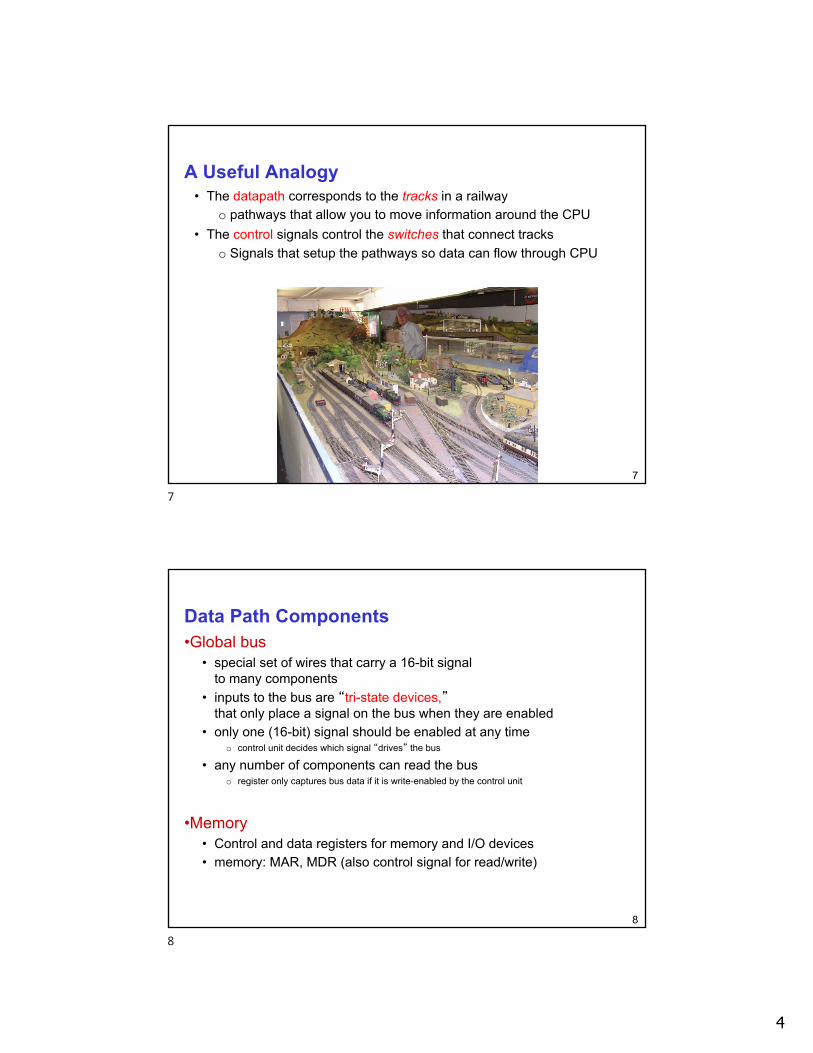
A Useful Analogy• The datapath corresponds to the tracks in a railway
o pathways that allow you to move information around the CPU• The control signals control the switches that connect tracks
o Signals that setup the pathways so data can flow through CPU
7
8
Data Path Components•Global bus
• special set of wires that carry a 16-bit signal to many components
• inputs to the bus are “tri-state devices,”that only place a signal on the bus when they are enabled
• only one (16-bit) signal should be enabled at any timeo control unit decides which signal “drives” the bus
• any number of components can read the buso register only captures bus data if it is write-enabled by the control unit
•Memory• Control and data registers for memory and I/O devices• memory: MAR, MDR (also control signal for read/write)
8

5
LC-3 Data Path- Components
Global bus is a set of wiresthat allow various components to transfer 16-bit data to other components.
One or more components may read data from the bus on any cycle.
Tri-state device determineswhich component puts dataon the bus. Only one sourceof data at any time.
9
LC-3 Data Path
Memory interface:MARMDRRead/Write control
10

6
11
Data Path Components•ALU
• Accepts inputs from register fileand from sign-extended bits from IR (immediate field).
o Bit 5 of LC3 instruction determines this
• Output goes to bus.o used by condition code logic, register file, memory
• Function to apply: determined by opcode – need 2 bits ALUK•Register File
• Two read addresses (SR1, SR2), one write address (DR)• Input from bus
o result of ALU operation or memory read
• Two 16-bit outputso used by ALU, PC, memory addresso data for store instructions passes through ALU
11
LC-3 Data Path
Register File (R0-R7)Control signals specify twosource register (SR1, SR2)and one destination (DR).
ALU performs ADD, AND, NOT.Operand A always comesfrom register file. Operand B isfrom register file or IR. Outputgoes to bus, to be written intoregister file.
Condition codes are setby looking at data placedon the bus by ALU or memory (MDR).
12

7
13
Data Path Components• PC and PCMUX
• Three inputs to PC, controlled by PCMUX1. PC+1 – FETCH stage2. Address adder – BR, JMP3. bus – TRAP (discussed later)
Ø MAR and MARMUX• Two inputs to MAR, controlled by MARMUX
1. Address adder – LD/ST, LDR/STR2. Zero-extended IR[7:0] -- TRAP (discussed later)
13
LC-3 Data Path
PC puts address on bus.Placed in MAR during Fetch.
PCMUX allows variousvalues to be written to PC: incremented PC (Fetch),computed address (BR), orregister data from bus (JMP).
IR gets data from bus (MDR)during Fetch.
14

8
LC-3 Data Path
MARMUX chooses valueto be written to MAR duringload, store, or TRAP.
Evaluate Address phaseadds offset to PC or registerfor load, store, BR.
15
16
Data Path Components•Condition Code Logic
• Looks at value on bus and generates N, Z, P signals• Registers set only when control unit enables them (LD.CC)
o only certain instructions set the codes(ADD, AND, NOT, LD, LDI, LDR, LEA)
•Control Unit – Finite State Machine• On each machine cycle, changes control signals for next phase
of instruction processingo who drives the bus? (GatePC, GateALU, …)o which registers are write enabled? (LD.IR, LD.REG, …)o which operation should ALU perform? (ALUK)o …
• Logic includes decoder for opcode, etc.
16

9
+1PC
FINITESTATE
MACHINE
REGFILE
SR2 SR1OUT OUT
MDR MARMEMORYLD.MDR
MEM.EN, R.W
GateMDR16
16
gatePC
ALU
SR2MUX
PCMUX
IR
16
LD.MAR
16
gateALU
R
DR
LD.REG
SR23
3
16
SR13
16
16
16
LD.IR
2
LD.PC
16
2
16
AB
PCMUX
INPUTKBDR
KBSR
OUTPUTDDR
DSR
Control
Proc
esso
r
The von Neumann components in
the Datapath
17
18
Instruction Execution and Datapath & Control Signals
• Examine the instruction execution process and the resulting dataflow • What devices are used• What control signals are needed to execute the instruction
o These signals are generated by the Control Unit– Implemented (conceptually) as a Finite State Machine
• Recall: instruction execution in LC3 (and all von Neumann) goes through the 6 phase instruction processing cycle
18

10
19
Instruction Processing Cycle – implementation of LC3 Datapath
Six phases of the complete Instruction Cycle
• 1. Fetch: load IR with instruction from memory
• 2. Decode: determine action to take (set up inputs for ALU, RAM, etc.)
• 3. Evaluate address: compute memory addr of operands, if any
• 4. Fetch operands: read operands from memory or registers
• 5. Execute: carry out instruction
• 6. Store results: write result to destination (register or memory)
19
20
Instruction Processing Step 1: FETCH•Load next instruction (at address stored in PC) from memory into Instruction Register (IR).• 1.Copy contents of PC into MAR: MAR ← (PC)• 2.Send “read” signal to mem and read: MDR ← (MAR)• 3.Copy contents of MDR into IR: IR ← MDR• 4. increment PC, so that it points to next inst
in sequence: PC = PC+1Step 4 and Step 1 can be done at the same cycle
EA
OP
EX
S
F
D
20

11
21MEM.EN, R.W
+1PC
FINITESTATE
MACHINE
MDR MARMEMORYLD.MDR
GateMDR16
16
gatePC
ADDR2MUX ADDR1MUX
PCMUX
+
SEXT
N Z P
LOGIC
16
IR
16
LD.MAR
16
R
[8:0]
016
LD.CC
16
LD.IR
2
2
LD.PC
ADDR2MUX
ADDR1MUX
16
16
16
PCMUX
LC3: Instruction Fetch
1
3
2
1
Branch inst:PC+Offset
Control signals:• LD.PC• gatePC• PCMUX• LD.MAR• MEM.EN,R• GateMDR• LD.CC• LD.IR• (ADDR2MUX• ADDR1MUX)
Logic neededfor branch & jump
21
22
Instruction Processing Step 2: DECODE•First identify the opcode.
• In LC-3, this is always the first four bits of instruction.o A 4-to-16 decoder asserts a control line corresponding
to the desired opcode.
•Depending on opcode, identify other operands from the remaining bits.
• Example:o for LDR, last six bits is offseto for ADD, last three bits is source operand #2
EA
OP
EX
S
F
D
22

12
23
Instruction Processing Cycle- Remaining steps• After Instruction fetch and decode, the next cycles are
evaluate address, operand fetch, execute, store.• To design datapath and control unit:
• What are the logic devices needed to execute instructions • What control signals should be generated by the control unit
• Consider three examples:1. ADD instruction execution2. LD (evaluate address, operand fetch and store into register)3. LDR (evaluate address, operand fetch and store into register)
23
ADD this zero means “register mode”
ADD:Dst= Src1 + Src2
R2= R1 + R3
Register mode:Operands are in registers
Use opcode to Set ALU todo Addition
24

13
ADD/AND (Immediate)
Note: Immediate field issign-extended.
this one means “immediate mode”
If Dst=010, Src1=001, Imm5=00011ADD R2,R1,#3
R2 = R1 +3
Immediate mode:One Operand in inst
25
26
REGFILE
SR2 SR1OUT OUT
ALU
SR2MUX
SEXT
IR
16 gateALU
[4:0]
0
DR
LD.REG
SR23
3
16
SR13
16
16
16
LD.IR
2
16
AB
ADD (AND) Instruction: LC3 Datapath
FINITESTATE
MACHINE
Control signals:• SR1, SR2, DR• LD.REG• SR2MUX• ALUK• gateALU
26

14
LD (PC-Relative)
If offset=#4 & PC=1000and dst= 011 (R3)Then load data from address 1000+4 = 1004 into register R3
offset
1004
abcd
abcd
1004
abcd
29
30
+1PC
FINITESTATE
MACHINE
SEXT
REGFILE
SR2 SR1OUT OUT
MDR MARMEMORY INPUT OUTPUTLD.MDR
MEM.EN, R.W
GateMDR16
16
gatePC
ALU
SR2MUX
MARMUX
ADDR2MUX ADDR1MUX
PCMUX
+
SEXT
SEXT
ZEXT
N Z P
LOGIC
SEXT
16
gateMARMUX
IR
16
LD.MAR
16
gateALU
R
[10:0]
[8:0]
[5:0]
[4:0]
0
16 16 16 16
LD.CC
1616
DR
LD.REG
SR23
3
16
SR13
16
1616
16
LD.IR
[7:0]2
2
LD.PC
ADDR2MUX
ADDR1MUX
16
16
16
2
16
AB
MARMUX
PCMUX
1
1
2
34
30
15
31
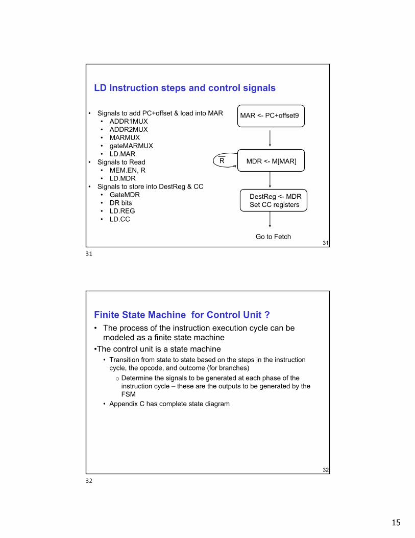
LD Instruction steps and control signals
MAR <- PC+offset9
MDR <- M[MAR]
DestReg <- MDRSet CC registers
Go to Fetch
R
• Signals to add PC+offset & load into MAR• ADDR1MUX• ADDR2MUX• MARMUX• gateMARMUX• LD.MAR
• Signals to Read• MEM.EN, R• LD.MDR
• Signals to store into DestReg & CC• GateMDR• DR bits• LD.REG• LD.CC
31
32
Finite State Machine for Control Unit ?• The process of the instruction execution cycle can be
modeled as a finite state machine•The control unit is a state machine
• Transition from state to state based on the steps in the instruction cycle, the opcode, and outcome (for branches)o Determine the signals to be generated at each phase of the
instruction cycle – these are the outputs to be generated by the FSM
• Appendix C has complete state diagram
32

16
33
The Instruction Cycle as FSMA simplified state diagram
33
34
The Instruction Cycle as FSMA simplified state diagram
At each state generate the required control signals:• Refer to datapath to determine which signals
• 1. gatePC, LD.MAR, LD.CC• 2. MEM.EN.R• 3. GateMDR, LD.IR
34

17
35
Complete FSM for LC3Control Unit
35
36
Implementing the Control Logic• Given the state diagram one can implement the controller in
many ways• 52 states• Each needs 39 control lines plus 10 to determine next state = 49
control lines• What should controller do ?
• Generate the 49 control signals at each cycle• Implement this as a Microprogram
• Use 6 bit address to get the microinstruction• Start state and progress through states based on microinstruction
36

18
37
Control Unit, Data Path, and Memory -Interactions
37
38
Microprogrammed Implementation
38

19
39
Datapath Summary
• Given an instruction set, we saw how each instruction’s execution is carried out• Requires setting control signals to “route the data”
• The control unit can be implemented as a FSM• At each state, it generates the value for the control signals• Transitions from state to state in one cycle
• For simpler implementation, the generation of the control signal by the FSM can be implemented using ”microinstructions”
• Designing a processor from scratch ?• Example of a simple processor design
39
EXAMPLE: BASIC CPUDATAPATH & CONTROL
40